WO2021206009A1 - 電子機器およびアクセサリ - Google Patents
電子機器およびアクセサリ Download PDFInfo
- Publication number
- WO2021206009A1 WO2021206009A1 PCT/JP2021/014288 JP2021014288W WO2021206009A1 WO 2021206009 A1 WO2021206009 A1 WO 2021206009A1 JP 2021014288 W JP2021014288 W JP 2021014288W WO 2021206009 A1 WO2021206009 A1 WO 2021206009A1
- Authority
- WO
- WIPO (PCT)
- Prior art keywords
- contact
- accessory
- contacts
- camera
- communication
- Prior art date
Links
- 238000004891 communication Methods 0.000 claims abstract description 261
- 238000001514 detection method Methods 0.000 claims abstract description 116
- 238000000034 method Methods 0.000 claims description 28
- 238000012545 processing Methods 0.000 claims description 19
- 101000686227 Homo sapiens Ras-related protein R-Ras2 Proteins 0.000 description 38
- 102100025003 Ras-related protein R-Ras2 Human genes 0.000 description 38
- 230000006870 function Effects 0.000 description 15
- 230000008569 process Effects 0.000 description 15
- 239000000758 substrate Substances 0.000 description 13
- 235000015429 Mirabilis expansa Nutrition 0.000 description 9
- 244000294411 Mirabilis expansa Species 0.000 description 9
- 235000013536 miso Nutrition 0.000 description 9
- 101000666657 Homo sapiens Rho-related GTP-binding protein RhoQ Proteins 0.000 description 7
- 102100038339 Rho-related GTP-binding protein RhoQ Human genes 0.000 description 7
- 230000007257 malfunction Effects 0.000 description 7
- 239000011347 resin Substances 0.000 description 7
- 229920005989 resin Polymers 0.000 description 7
- 230000008859 change Effects 0.000 description 6
- 239000002184 metal Substances 0.000 description 6
- 230000005540 biological transmission Effects 0.000 description 5
- 239000000463 material Substances 0.000 description 5
- 230000003068 static effect Effects 0.000 description 5
- 230000001360 synchronised effect Effects 0.000 description 5
- 230000003287 optical effect Effects 0.000 description 4
- 230000004044 response Effects 0.000 description 4
- 101000702105 Rattus norvegicus Sproutin Proteins 0.000 description 3
- 230000000694 effects Effects 0.000 description 3
- 239000012811 non-conductive material Substances 0.000 description 3
- 239000011295 pitch Substances 0.000 description 3
- 238000005070 sampling Methods 0.000 description 3
- HEZMWWAKWCSUCB-PHDIDXHHSA-N (3R,4R)-3,4-dihydroxycyclohexa-1,5-diene-1-carboxylic acid Chemical compound O[C@@H]1C=CC(C(O)=O)=C[C@H]1O HEZMWWAKWCSUCB-PHDIDXHHSA-N 0.000 description 2
- 230000002159 abnormal effect Effects 0.000 description 2
- 238000013461 design Methods 0.000 description 2
- 238000003384 imaging method Methods 0.000 description 2
- 238000012986 modification Methods 0.000 description 2
- 230000004048 modification Effects 0.000 description 2
- 230000005856 abnormality Effects 0.000 description 1
- 230000006399 behavior Effects 0.000 description 1
- 238000005452 bending Methods 0.000 description 1
- 239000003990 capacitor Substances 0.000 description 1
- 238000006243 chemical reaction Methods 0.000 description 1
- 230000000052 comparative effect Effects 0.000 description 1
- 238000004590 computer program Methods 0.000 description 1
- 230000007547 defect Effects 0.000 description 1
- 239000003989 dielectric material Substances 0.000 description 1
- 238000005286 illumination Methods 0.000 description 1
- 238000003780 insertion Methods 0.000 description 1
- 230000037431 insertion Effects 0.000 description 1
- 230000002452 interceptive effect Effects 0.000 description 1
- 238000000465 moulding Methods 0.000 description 1
- 230000002093 peripheral effect Effects 0.000 description 1
- 230000005855 radiation Effects 0.000 description 1
- 230000009467 reduction Effects 0.000 description 1
- 238000000926 separation method Methods 0.000 description 1
- 238000012546 transfer Methods 0.000 description 1
- 229910052724 xenon Inorganic materials 0.000 description 1
- FHNFHKCVQCLJFQ-UHFFFAOYSA-N xenon atom Chemical compound [Xe] FHNFHKCVQCLJFQ-UHFFFAOYSA-N 0.000 description 1
Images


Classifications
-
- G—PHYSICS
- G03—PHOTOGRAPHY; CINEMATOGRAPHY; ANALOGOUS TECHNIQUES USING WAVES OTHER THAN OPTICAL WAVES; ELECTROGRAPHY; HOLOGRAPHY
- G03B—APPARATUS OR ARRANGEMENTS FOR TAKING PHOTOGRAPHS OR FOR PROJECTING OR VIEWING THEM; APPARATUS OR ARRANGEMENTS EMPLOYING ANALOGOUS TECHNIQUES USING WAVES OTHER THAN OPTICAL WAVES; ACCESSORIES THEREFOR
- G03B17/00—Details of cameras or camera bodies; Accessories therefor
- G03B17/02—Bodies
- G03B17/12—Bodies with means for supporting objectives, supplementary lenses, filters, masks, or turrets
- G03B17/14—Bodies with means for supporting objectives, supplementary lenses, filters, masks, or turrets interchangeably
-
- G—PHYSICS
- G03—PHOTOGRAPHY; CINEMATOGRAPHY; ANALOGOUS TECHNIQUES USING WAVES OTHER THAN OPTICAL WAVES; ELECTROGRAPHY; HOLOGRAPHY
- G03B—APPARATUS OR ARRANGEMENTS FOR TAKING PHOTOGRAPHS OR FOR PROJECTING OR VIEWING THEM; APPARATUS OR ARRANGEMENTS EMPLOYING ANALOGOUS TECHNIQUES USING WAVES OTHER THAN OPTICAL WAVES; ACCESSORIES THEREFOR
- G03B15/00—Special procedures for taking photographs; Apparatus therefor
- G03B15/02—Illuminating scene
- G03B15/03—Combinations of cameras with lighting apparatus; Flash units
- G03B15/05—Combinations of cameras with electronic flash apparatus; Electronic flash units
-
- G—PHYSICS
- G03—PHOTOGRAPHY; CINEMATOGRAPHY; ANALOGOUS TECHNIQUES USING WAVES OTHER THAN OPTICAL WAVES; ELECTROGRAPHY; HOLOGRAPHY
- G03B—APPARATUS OR ARRANGEMENTS FOR TAKING PHOTOGRAPHS OR FOR PROJECTING OR VIEWING THEM; APPARATUS OR ARRANGEMENTS EMPLOYING ANALOGOUS TECHNIQUES USING WAVES OTHER THAN OPTICAL WAVES; ACCESSORIES THEREFOR
- G03B17/00—Details of cameras or camera bodies; Accessories therefor
- G03B17/56—Accessories
- G03B17/565—Optical accessories, e.g. converters for close-up photography, tele-convertors, wide-angle convertors
-
- G—PHYSICS
- G03—PHOTOGRAPHY; CINEMATOGRAPHY; ANALOGOUS TECHNIQUES USING WAVES OTHER THAN OPTICAL WAVES; ELECTROGRAPHY; HOLOGRAPHY
- G03B—APPARATUS OR ARRANGEMENTS FOR TAKING PHOTOGRAPHS OR FOR PROJECTING OR VIEWING THEM; APPARATUS OR ARRANGEMENTS EMPLOYING ANALOGOUS TECHNIQUES USING WAVES OTHER THAN OPTICAL WAVES; ACCESSORIES THEREFOR
- G03B7/00—Control of exposure by setting shutters, diaphragms or filters, separately or conjointly
- G03B7/26—Power supplies; Circuitry or arrangement to switch on the power source; Circuitry to check the power source voltage
-
- G—PHYSICS
- G03—PHOTOGRAPHY; CINEMATOGRAPHY; ANALOGOUS TECHNIQUES USING WAVES OTHER THAN OPTICAL WAVES; ELECTROGRAPHY; HOLOGRAPHY
- G03B—APPARATUS OR ARRANGEMENTS FOR TAKING PHOTOGRAPHS OR FOR PROJECTING OR VIEWING THEM; APPARATUS OR ARRANGEMENTS EMPLOYING ANALOGOUS TECHNIQUES USING WAVES OTHER THAN OPTICAL WAVES; ACCESSORIES THEREFOR
- G03B2206/00—Systems for exchange of information between different pieces of apparatus, e.g. for exchanging trimming information, for photo finishing
-
- G—PHYSICS
- G03—PHOTOGRAPHY; CINEMATOGRAPHY; ANALOGOUS TECHNIQUES USING WAVES OTHER THAN OPTICAL WAVES; ELECTROGRAPHY; HOLOGRAPHY
- G03B—APPARATUS OR ARRANGEMENTS FOR TAKING PHOTOGRAPHS OR FOR PROJECTING OR VIEWING THEM; APPARATUS OR ARRANGEMENTS EMPLOYING ANALOGOUS TECHNIQUES USING WAVES OTHER THAN OPTICAL WAVES; ACCESSORIES THEREFOR
- G03B2215/00—Special procedures for taking photographs; Apparatus therefor
- G03B2215/05—Combinations of cameras with electronic flash units
- G03B2215/0514—Separate unit
- G03B2215/056—Connection with camera, e.g. adapter
-
- H—ELECTRICITY
- H04—ELECTRIC COMMUNICATION TECHNIQUE
- H04N—PICTORIAL COMMUNICATION, e.g. TELEVISION
- H04N23/00—Cameras or camera modules comprising electronic image sensors; Control thereof
- H04N23/56—Cameras or camera modules comprising electronic image sensors; Control thereof provided with illuminating means
Definitions
- the present invention relates to electronic devices and accessories having contacts used for communication, mounting detection, and the like.
- the accessory shoe is provided with a plurality of contacts (terminals) for detecting the attachment of the accessory to the camera and for communicating between the camera and the accessory.
- the present invention provides an electronic device and an accessory capable of reducing the occurrence of a communication error due to some terminals becoming non-contact when the accessory is attached.
- accessories are detachably attached, and a plurality of contacts electrically connected to the accessories are arranged in a row.
- the plurality of contacts include a mounting detection contact used for detecting the mounting of an accessory on an electronic device and a communication request contact used for a communication request from the accessory to the electronic device.
- the mounting detection contact and the communication request contact are arranged between the contact on the one end side and the contact on the other end side in the arrangement direction of the plurality of contacts.
- the mounting detection contact is arranged between the communication request contact and the contact on the farthest end side. In the arrangement direction of the contacts, the distance between the mounting detection contact and the communication request contact is shorter than the distance between the communication request contact and the contact on the farthest end side.
- the accessory as another aspect of the present invention is detachably attached to an electronic device, and a plurality of contacts electrically connected to the electronic device are arranged in a row.
- the plurality of contacts include a mounting detection contact used for detecting the mounting of an accessory on an electronic device and a communication request contact used for a communication request from the accessory to the electronic device.
- the mounting detection contact and the communication request contact are arranged between the contact on the one end side and the contact on the other end side in the arrangement direction of the plurality of contacts.
- the mounting detection contact is arranged between the communication request contact and the contact on the farthest end side. In the arrangement direction of the contacts, the distance between the mounting detection contact and the communication request contact is shorter than the distance between the communication request contact and the contact on the farthest end side.
- a system including the electronic device and the accessory also constitutes another aspect of the present invention.
- the figure which shows the structure of the camera and the accessory in embodiment of this invention The figure which shows the camera which attached the accessory in embodiment, and the arrangement example of the contact point with them. The figure which shows how the external force is applied to the accessory attached to the camera in embodiment. The figure which shows the structure for determining the connection state of the ground contact in an embodiment.
- the flowchart which shows the process executed by the camera in embodiment The flowchart which shows the process executed by the camera of embodiment.
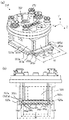
- FIG. 3 is a perspective view of an external flash unit which is a camera and an accessory in the embodiment. Exploded view and perspective view of the accessory shoe in the embodiment. The figure which shows the structure of the engaging member of the accessory shoe and the connection terminal connector in embodiment.
- a perspective view and a cross-sectional view of the external flash unit according to the embodiment.
- the front sectional view which shows the state which the camera connection part was attached to the accessory shoe in embodiment.
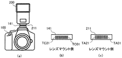
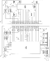
- FIG. 1 shows an electrical configuration of a camera 100 as an electronic device according to an embodiment of the present invention and an accessory 200 detachably attached to the camera 100.
- the plurality of contacts (terminals) TC01 to TC21 of the camera connection portion 141 provided in the camera 100 and the plurality of contacts TA01 to TA21 of the accessory connection portion 211 provided in the accessory 200 are one-to-one, respectively. It is electrically connected by contacting with.
- the camera 100 is supplied with electric power from the battery 111.
- the battery 111 can be attached to and detached from the camera 100.
- the camera control circuit 101 as a control means of the camera 100 is a circuit that controls the entire camera 100, and is composed of a microcomputer having a built-in CPU or the like.
- the system power supply circuit 112 is a circuit that generates power for supplying power to each circuit of the camera 100, and is composed of a DCDC converter circuit, an LDO (Low Drop Out), a charge pump circuit, and the like.
- the voltage 1.8V generated by the system power supply circuit 112 is constantly supplied from the battery 111 to the camera control circuit 101 as the camera microcomputer power supply VMCU_C.
- the camera control circuit 101 controls the system power supply circuit 112 to turn on / off the power supply to each circuit of the camera 100.
- the optical lens 121 is removable from the camera 100.
- the light from the subject incident through the optical lens 121 is imaged on the image pickup sensor 122 including a CMOS sensor, a CCD sensor, or the like.
- the subject image formed on the image pickup sensor 122 is encoded into a digital image pickup signal.
- the image processing circuit 123 performs image processing such as noise reduction processing and white balance processing on the digital image pickup signal to generate image data, and in order to record the image data in the recording memory 126, a PEG format or the like is used. Convert to an image file of. Further, the image processing circuit 123 generates VRAM image data for display on the display circuit 127 from the image data.
- the memory control circuit 124 controls the transmission and reception of image data and other data generated by the image processing circuit 123 and the like.
- the volatile memory 125 is a memory capable of high-speed reading and writing such as DDR3 SDRAM, and is used for an image processing workspace or the like performed by the image processing circuit 123.
- the recording memory 126 is a readable and writable recording medium such as an SD card or CFexpress card that can be attached to and detached from the camera 100 via a connection portion (not shown).
- the display circuit 127 is a display arranged on the back surface of the camera 100, and is composed of an LCD panel, an organic EL display panel, and the like.
- the backlight circuit 128 adjusts the brightness of the display circuit 127 by changing the amount of light from the backlight of the display circuit 127.
- the accessory power supply circuit A131 and the accessory power supply circuit B132 as the power supply means are voltage conversion circuits that convert the voltage supplied from the system power supply circuit 112 into a predetermined voltage, respectively. Generates .3V.
- the accessory power supply circuit A131 is a power supply circuit composed of an LDO or the like and having low self-consumption.
- the accessory power supply circuit B132 is a circuit composed of a DC / DC converter circuit or the like and capable of passing a larger current than the accessory power supply circuit A131.
- the self-consumption of the accessory power supply circuit B132 is larger than that of the accessory power supply circuit A131. Therefore, when the load current is small, the accessory power supply circuit A131 is more efficient than the accessory power supply circuit B132, and when the load current is large, the accessory power supply circuit B132 is more efficient than the accessory power supply circuit A131.
- the camera control circuit 101 controls on / off of the voltage output of the accessory power supply circuit A131 and the accessory power supply circuit B132 according to the operating state of the accessory 200.
- the protection circuit 133 as a protection means is composed of a current fuse element, a polyswitch element, an electronic fuse circuit that combines a resistor, an amplifier, and a switch element, and the like, from the accessory power supply circuit A131 and the accessory power supply circuit B132 to the accessory 200.
- the overcurrent detection signal DET_OVC is output.
- the protection circuit 133 is an electronic fuse circuit, and when a current of 1 A or more flows, the camera control circuit 101 is notified by an overcurrent detection signal DET_OVC.
- the overcurrent detection signal DET_OVC indicates that the overcurrent is due to the Hi level.
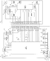
- the camera connection unit 141 is a connector for making an electrical connection with the accessory 200 via 21 contacts TC01 to TC21 arranged in a row.
- the contacts TC01 to TC21 are arranged in this order from one end to the other end in the arrangement direction thereof.
- the TC01 is connected to the ground (GND) and is used not only as a contact for the reference potential (GND potential) but also as a contact for controlling the wiring impedance of the differential signal D1N and the differential signal D1P described below. ing. TC01 corresponds to the third ground contact.
- the differential signal D1N connected to the TC02 and the differential signal D1P connected to the TC03 are differential data communication signals that perform data communication in pairs, and are connected to the camera control circuit 101.
- TC02, TC03, TC07 to TC17, TC19 and TC20, which will be described later, are communication contacts.
- TC04 as the first ground contact is connected to GND and serves as a reference potential contact between the camera 100 and the accessory 200.
- the TC04 is arranged outside the TC05 described below in the contact arrangement direction.
- the accessory power supply VACC generated by the accessory power supply circuits A131 and B132 is connected to the TC05 as the power supply contact via the protection circuit 133.
- the accessory mounting detection signal / ACC_DET is connected to TC06 as the mounting detection contact.
- the accessory mounting detection signal / ACC_DET is pulled up to the camera microcomputer power supply VMCU_C via the resistance element Rp134 (10 k ⁇ ).
- the camera control circuit 101 can detect whether or not the accessory 200 is attached by reading the accessory attachment detection signal / ACC_DET signal level. If the accessory mounting detection signal / ACC_DET signal level (potential) is Hi level (predetermined potential), accessory 200 is detected as not mounted, and if it is Lo level (GND potential as described later), accessory 200 is mounted. Detected.
- the accessory mounting detection signal / ACC_DET signal level (potential) changes from the Hi level to the Lo level as a trigger, and various transmissions are performed between the camera 100 and the accessory 200 via contacts.
- the camera control circuit 101 supplies power to the accessory 200 via the TC05 as a power contact in response to detecting that the accessory 200 is in the mounted state.
- the camera control circuit 101 acts as a communication master to perform SPI (Serial Peripheral Interface) communication. It is a signal.
- SPI Serial Peripheral Interface
- the communication clock frequency of SPI communication is 1 MHz.
- a communication request signal / WAKE for requesting communication from the accessory 200 to the camera control circuit 101 is connected to the TC11.
- the communication request signal / WAKE is pulled up to the camera microcomputer power supply VMCU_C via a resistor.
- the camera control circuit 101 can receive the communication request from the accessory 200 by detecting the communication request signal / the falling edge of WAKE.
- the SDA connected to the TC12 and the SCL connected to the TC13 are signals for the camera control circuit 101 to act as a communication master and perform I2C (Inter-Integrated Circuit) communication.
- the SDA and SCL are signals for open-drain communication (hereinafter referred to as open-drain communication) pulled up to the camera microcomputer power supply VMCU_C, and the communication frequency is 100 kbps in this embodiment.
- I2C communication both data transmission from the camera 100 and data transmission from the accessory 200 are performed via the SDA. Comparing SPI communication and I2C communication, I2C communication has a lower communication speed than SPI communication, and communication with low power consumption is possible. Further, SPI communication has a higher communication speed than I2C communication, and is therefore suitable for communication of information having a large amount of data. Therefore, in the communication between the camera 100 and the accessory 200 of the present embodiment, the information having a large amount of data is communicated by using SPI communication, and the information having a small amount of data is communicated by using I2C communication. For example, data is first communicated using I2C communication, and when SPI communication can be executed or SPI communication needs to be executed based on this data, control is performed so that SPI communication is further executed. Can be done.
- the FNC1 signal connected to the TC14 (synchronous contact), the FNC2 signal connected to the TC15, the FNC3 signal connected to the TC16, and the FNC4 signal connected to the TC17 change their functions according to the type of accessory 200 installed. It is a possible signal.
- the signal communicated via the TC 15 is an audio data signal.
- the signal communicated via the TC 14 is a signal for controlling the timing of light emission.
- signals that realize different functions may be communicated via the same contact.
- a synchronization signal for controlling a timing different from the light emission timing may be communicated via the TC14.
- TC14 to TC17 correspond to functional signal contacts. Communication using at least one of the functional signal contacts is also referred to as functional signal communication.
- Functional signal communication can execute communication at a timing that does not depend on I2C communication / SPI communication in parallel with I2C communication / SPI communication.
- the types of accessories referred to here are the above-mentioned microphone devices, lighting devices, and the like. Accessories that achieve the same purpose, such as lights with different performances, are the same type of accessory. Accessories that achieve different purposes, such as microphone and lighting equipment, are different types of accessories.
- Functional signal communication is executed based on the information acquired by I2C communication or SPI communication.
- the TC18 as the second ground contact is also connected to GND, and is the contact that serves as the reference potential between the camera 100 and the accessory 200, like the TC04.
- the differential signal D2N connected to TC19 (first differential signal contact) and the differential signal D2P connected to TC20 (second differential signal contact) are data in which they perform data communication in pairs. It is a communication signal and is connected to the camera control circuit 101. For example, USB communication can be performed via TC19 and TC20.
- the TC21 is connected to GND and is used not only as a contact for a reference potential but also as a contact for controlling the wiring impedance of the differential signal D2N and the differential signal D2P.
- TC21 corresponds to the fourth ground contact.
- the contacts TC01, TC04, TC06, TC18, and TC21 are connected to, for example, the GND portion of the flexible substrate 158 shown in FIG. 17, which will be described later, and the GND portion of the flexible substrate 158 becomes the GND level of the camera 100. It is fixed at 157 or the like.
- Metallic members having a GND level include, for example, an engaging member 151, a base plate (not shown) inside the camera 100, and the like.
- the mounting detection contact TC06 to which the accessory mounting detection signal / ACC_DET is connected is arranged next to the contact (first clock contact) TC07 that transmits the clock signal SCLK (first clock signal). doing.
- noise clock noise
- SCLK first clock signal
- the accessory mounting detection signal / ACC_DET is pulled up before the accessory is mounted, but is set to the GND potential after the accessory is mounted.
- the SCLK contact TC07 that transmits the clock signal does not transmit the clock signal before the accessory is attached, the potential does not fluctuate, and the potential fluctuates because the clock signal is transmitted only after the accessory is attached.
- the mounting detection contact TC06 When the SCLK contact TC07 transmits a clock signal, the mounting detection contact TC06 is at the GND potential. Therefore, even if the mounting detection contact TC06 receives clock noise, the potential of the control circuit of the camera 100 or the accessory 200 is unlikely to fluctuate, so that malfunction can be prevented. In addition, it is possible to suppress the transmission of clock noise to a position farther than the mounting detection contact TC06. As a result, since it is not necessary to arrange the GND terminal, the influence of clock noise can be suppressed without increasing the number of contacts.
- SCL second clock signal
- SCLK second clock signal
- the frequency of SCLK transmitted to the SCLK contact TC07 is higher than that of the SCL, and the SCLK contact TC07 generates more clock noise than the SCL contact TC13. Therefore, if the mounting detection contact TC06 is arranged next to the SCLK contact TC07 instead of next to the SCL contact TC13, the effect of preventing malfunction due to clock noise is greater.
- the SCL transmitted by the SCL contact TC13 is a clock signal of the I2C communication standard, and the fluctuation of the voltage of the signal line is driven by the open drain connection.
- the SCLK transmitted by the SCLK contact TC07 is a clock signal of the SPI communication standard, and the fluctuation of the voltage of the signal line is driven by the CMOS output. Therefore, the SCL contact TC13 tends to have a gentler edge of voltage fluctuation than the SCLK contact TC07, and clock noise is less likely to occur. Therefore, arranging the mounting detection contact TC06 next to the SCLK contact TC07 rather than next to the SCL contact TC13 is more effective in preventing malfunction due to clock noise.
- the differential signals D1N and D1P may be transmitted in pairs to the first and second differential signal contacts TC19 and TC20 to transmit the clock signal.
- a clock signal (third clock signal) having a frequency higher than that of the SCLK contact TC07 and the SCL contact TC13 may be transmitted.
- the differential signals D1N and D1P are pair signals, the emission of clock noise is smaller than that of the SCLK contact TC07 and the SCL contact TC13 that transmit the single-ended signal. Therefore, it is more effective to prevent the malfunction due to the clock noise by arranging the mounting detection contact TC06 next to the SCLK contact TC07 instead of next to the first and second differential signal contacts TC19 and TC20.
- the contact (first data contact) TC08 arranged next to the mounting detection contact TC06 of the SCLK contact TC07 transmits MOSI (first data signal). Since MOSI is a data signal, it appears to be susceptible to clock noise. However, since the MOSI is a data signal of the same SPI communication standard as the clock signal transmitted by the SCLK contact TC07, the fluctuation timing of the potential is synchronized with the clock signal and is not easily affected by the clock noise. Therefore, the contact TC08 does not have to be fixed to the GND potential and can be used as a MOSI contact.
- the accessory 200 has a battery 205 and receives power supply from the battery 205 and also receives power supply from the camera 100 via the camera connection unit 141 and the accessory connection unit 211.
- the accessory control circuit 201 as a control means of the accessory 200 is a circuit that controls the entire accessory 200, and is a microcomputer having a built-in CPU and the like.
- the accessory power supply circuit 202 is a circuit that generates a power supply for supplying power to each circuit of the accessory 200, and is composed of a DCDC converter circuit, an LDO, a charge pump circuit, and the like.
- the voltage 1.8V generated by the accessory power supply circuit 202 is constantly supplied to the accessory control circuit 201 as the accessory microcomputer power supply VMCU_A. By controlling the accessory power supply circuit 202, on / off control of power supply to each circuit of the accessory 200 is performed.
- the charging circuit 204 is a circuit for charging the battery 205 using the electric power supplied from the camera 100.
- the accessory control circuit 201 controls the charging circuit 204 to charge the battery 205.
- the accessory 200 may operate only by supplying power from the camera 100 without mounting the battery 205. In this case, the charging circuit 204 becomes unnecessary.
- the differential communication circuit 207 is a circuit for performing differential communication with the camera 100, and can transmit and receive data to and from the camera 100.
- the external communication IF circuit 208 is an IF circuit for performing data communication with an external device (not shown), such as an Ethernet communication IF, a wireless LAN communication IF, and a public network communication IF.
- the accessory control circuit 201 controls the differential communication circuit 207 and the external communication IF circuit 208 to transmit the data received from the camera 100 to the external device or the data received from the external device to the camera 100. be able to.
- the functional circuit 206 is a circuit having different functions depending on the type of the accessory 200. A configuration example of the functional circuit 206 will be described later.
- the external connection terminal 209 is a connector terminal for connecting to an external device, and is a USB TYPE-C connector in this embodiment.
- the connection detection circuit 210 is a circuit for detecting that an external device is connected to the external connection terminal 209, and the accessory control circuit 201 connects to the external connection terminal 209 by receiving the output signal of the connection detection circuit 210. External device connection can be detected.
- the power switch 203 is a switch for turning on / off the operation of the accessory 200, and the accessory control circuit 201 can detect the on position and the off position by reading the signal level of the terminal to which the power switch 203 is connected.
- the accessory connection unit 211 is a connector for electrically connecting to the camera 100 via 21 contacts TA01 to TA21 arranged in a row.
- the contacts TA01 to TA21 are arranged in this order from one end to the other end in the arrangement direction.
- the TA01 is connected to GND and can be used not only as a contact for a reference potential but also as a contact for controlling the wiring impedance of the differential signal D1N and the differential signal D1P.
- TA01 corresponds to the third ground contact.
- the differential signal D1N connected to TA02 and the differential signal D1P connected to TA03 are data communication signals in which they perform data communication in pairs, and are connected to the differential communication circuit 207.
- TA02, TA03, TA07 to TA17, TA19 and TA20 described later are communication contacts.
- TA04 as the first ground contact is connected to GND and serves as a reference potential contact between the camera 100 and the accessory 200.
- the TA04 is arranged outside the TA05 described below in the contact arrangement direction.
- the accessory power supply circuit 202 and the charging circuit 204 are connected to the TA05 as the power supply contact, and the accessory power supply VACC supplied from the camera 100 is connected.
- the TA06 as a mounting detection contact is directly connected to the GND, and when the accessory 200 is mounted on the camera 100, the accessory mounting detection signal / ACC_DET described above is set to the GND level as the Lo level. As a result, it becomes a contact point for causing the camera 100 to detect the attachment of the accessory 200.
- the SCLK connected to TA07, the MOSI connected to TA08, the MISO connected to TA09, and the CS connected to TA10 are signals for the accessory control circuit 201 to act as a communication slave for SPI communication.
- a communication request signal / WAKE for requesting communication from the camera 100 from the accessory control circuit 201 is connected to the TA11.
- the accessory control circuit 201 determines that communication with the camera 100 is necessary, the accessory control circuit 201 makes a communication request to the camera 100 by outputting a communication request signal / WAKE Lo.
- the accessory control circuit 201 When power is supplied from the camera control circuit 101 to the accessory 200 via the TC5 in response to detecting that the accessory 200 is in the mounted state, the accessory control circuit 201 receives a communication request signal / WAKE signal level ( By changing the potential) from the Hi level to the Lo level, the camera control circuit 101 is notified that the power supply has been received.
- the accessory control circuit 201 changes the communication request signal / WAKE signal level (potential) from the Hi level to the Lo level even if there is no request from the camera, so that a factor that causes the accessory 200 to communicate with the camera 100 has occurred. Can be notified. With this configuration, the camera control circuit 101 can omit the operation of periodically checking whether or not a factor for communication has occurred in the accessory 200 by polling. In addition, the accessory 200 can communicate to the camera 100 in real time when a factor to be communicated occurs.
- the SDA connected to the TA12 and the SCL connected to the TA13 are signals for the accessory control circuit 201 to act as a communication slave and perform I2C communication.
- the FNC1 signal connected to the TA14 (synchronous contact), the FNC2 signal connected to the TA15, the FNC3 signal connected to the TA16, and the FNC4 signal connected to the TA17 are signals whose functions can be changed according to the type of the accessory 200. Is. For example, when the accessory 200 is a microphone device, it is a voice data signal, and when the accessory 200 is a strobe device, it is a signal for controlling the timing of light emission.
- TA14 to TA17 correspond to functional signal contacts.
- the TA18 as the second ground contact is also connected to GND, and like the TA04, it becomes the reference potential contact between the camera 100 and the accessory 200.
- the differential signal D2N connected to TA19 (first differential signal contact) and the differential signal D2P connected to TA20 (second differential signal contact) are data in which they are paired to perform data communication. It is a communication signal and is connected to the external connection terminal 209.
- the TA21 is connected to GND and can be used not only as a contact point for a reference potential but also as a terminal for controlling the wiring impedance of the differential signal D2N and the differential signal D2P.
- TA21 corresponds to the fourth ground contact.
- the contacts TA01, TA04, TA06, TA18, and TA21 are connected to, for example, the GND portion of the flexible substrate 259 shown in FIG. 19 described later, and the GND portion of the flexible substrate 259 is not a metallic member that becomes the GND level of the accessory 200. It is fixed with the screws shown in the figure.
- Metallic members having a GND level include, for example, a shoe mounting leg 251 and a base plate (not shown) inside the accessory 200.
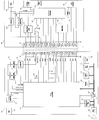
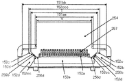
- FIG. 2A the accessory connecting portion 211 arranged on the shoe provided on the lower part of the accessory (strobe device) 200 is connected to the camera connecting portion 141 arranged on the accessory shoe provided on the upper part of the camera 100. It shows the state that was done.
- FIG. 2B shows an arrangement example of 21 contacts TC01 to TC21 in the camera connection portion 141. TC01 is arranged at the right end when viewed from the subject side, and 21 contacts up to TC21 are arranged in a row. The accessory shoe is attached by sliding from the upper side to the lower side in FIG. 2B with respect to the accessory shoe having the camera connection portion 141.
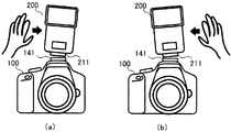
- FIG. 2C shows an arrangement example of 21 contacts TA01 to TA21 in the accessory connection portion 211. Similar to the camera connection portion 141, the TA01 is arranged at the right end when viewed from the subject side, and 21 contacts up to the TA21 are arranged in a row. Normally, the contacts TA01 to TA21 and the corresponding contacts TC01 to TC21 are in contact with each other. However, if excessive static pressure or impact is applied to the accessory 200, the contacts may be separated from each other. In particular, when a force in the rotational direction acts on the direction in which the contacts are lined up in the accessory 200, contact separation is likely to occur at the end contacts.
- FIG. 3A exaggerates the appearance of excessive static pressure applied to the accessory 200 from the left side when viewed from the subject side.
- a force acts on the contacts TC21, TA21 of the camera connecting portion 141 and the accessory connecting portion 211 and the contacts in the vicinity thereof in the direction in which the contacts are separated from each other, and poor contact is likely to occur.
- a force acts on the contacts TC01 and TA01 and the contacts in the vicinity thereof in the direction of contact more than in the normal state.
- FIG. 3B exaggerates the appearance of excessive static pressure applied to the accessory 200 from the right side when viewed from the subject side.
- a force acts on the contacts TC01 and TA01 of the camera connecting portion 141 and the accessory connecting portion 211 and the contacts in the vicinity thereof in the direction in which the contacts are separated from each other, and poor contact is likely to occur.
- a force acts on the contacts TC21, TA21 and the contacts in the vicinity thereof in the direction of contact more than in the normal state.
- the contacts TC01, TA01 and TC21, TA21 at both ends of the camera connecting portion 141 and the accessory connecting portion 211 are connected to the GND.
- the GND connection can be secured at the contact at the other end. Therefore, the reference potential of the accessory 200 becomes unstable due to the poor GND connection, and as a result, the risk of damage to each circuit or electric element can be reduced.
- the camera control circuit 101 cannot detect that a part of the GND contacts is missing when the accessory 200 without some GND contacts is attached due to a defect failure of the accessory connection portion 211 or the like. In such a case, the operating current is concentrated on the remaining GND contacts, and there is a concern that the accessory 200 may malfunction in some cases.
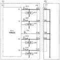
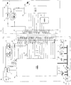
- FIG. 4A is an example of a configuration for allowing the camera 100 to detect the connection state of the GND contact of the accessory 200, and shows an excerpt of a portion related to the ground contact from the configuration shown in FIG.
- TC01, TC04, TC18 and TC21 are connected to the input terminals P1, P2, P3 and P4 of the camera control circuit 101, respectively, and are pulled to the camera microcomputer power supply VMCU_C via the resistors 1011Rp_g1, the resistors 1021Rp_g2, the resistors 1031Rp_g3 and the resistors 1041Rp_g4, respectively. It has been uploaded. Further, SW circuit 1 (1012), SW circuit 2 (1022), SW circuit 3 (1032) and SW circuit 4 (1042) are connected to TC01, TC04, TC18 and TC21, respectively.
- the SW circuit 1 is a switch circuit driven by the control signal of the camera control circuit 101, and when it is turned on by the control signal, the TC01 is connected to GND. It is desirable that the SW circuit 1 is composed of, for example, FETs, the impedance when the operation is on is as small as possible, and the impedance when the operation is off is as large as possible.
- the SW circuit 2, the SW circuit 3, and the SW circuit 4 also have the same configuration as the SW circuit 1 as shown in FIG. 4A.
- the flowchart of FIG. 4B shows a sequence for determining the connection state of the ground terminal in the configuration shown in FIG. 4A.
- the camera control circuit 101 executes this process and other processes described later according to a computer program.
- S means a step.
- the camera control circuit 101 monitors the accessory mounting detection signal / ACC_DET signal level and determines whether or not the accessory 200 is mounted. If the signal level is Hi, the camera control circuit 101 returns to S1001 and performs detection again, assuming that the accessory 200 is not attached, and if the signal level is Lo, proceeds to S1002 assuming that the accessory 200 is attached.
- the camera control circuit 101 controls to turn on the SW circuit 1 and turn off the SW circuit 2, the SW circuit 3, and the SW circuit 4, respectively.
- the camera control circuit 101 confirms the voltage level of the input terminal P1, determines that TC01 is connected to the ground contact if it is Lo level, and that it is not connected to the ground contact if it is Hi level. judge.
- the camera control circuit 101 controls to turn on the SW circuit 2 and turn off the SW circuit 1, the SW circuit 3, and the SW circuit 4, respectively.
- the camera control circuit 101 confirms the voltage level of the input terminal P2, determines that the TC04 is connected to the ground contact if it is Lo level, and that it is not connected to the ground contact if it is Hi level. judge.
- the camera control circuit 101 controls to turn on the SW circuit 3 and turn off the SW circuit 1, the SW circuit 2, and the SW circuit 4, respectively.
- the camera control circuit 101 confirms the voltage level of the input terminal P3, and if it is Lo level, it is determined that TC18 is connected to the ground contact, and if it is Hi level, it is determined that it is not connected to the ground contact. ..
- the camera control circuit 101 controls to turn on the SW circuit 4 and turn off the SW circuit 1, the SW circuit 2, and the SW circuit 3, respectively.
- the camera control circuit 101 confirms the voltage level of the input terminal P4, determines that the TC18 is connected to the ground contact if it is Lo level, and that it is not connected to the ground contact if it is Hi level. judge.
- the camera control circuit 101 controls to turn on the SW circuit 1, the SW circuit 2, the SW circuit 3, and the SW circuit 4, respectively.
- the accessory 200 is tilted with respect to the camera 100 when the accessory 200 is attached to the camera 100, only some of the plurality of contacts TC01 to TC21 and TA01 to TA21 come into contact with each other. obtain.
- the mounting direction of the accessory 200 with respect to the camera 100 is the Z direction
- the direction in which the plurality of contacts TC01 to TC21 and TA01 to TA21 are lined up is the X direction
- the direction orthogonal to the X direction and the Z direction is the Y direction.
- the attachment detection process is executed prior to various communications in the state where the accessory 200 is attached to the camera 100.
- the mounting detection process can be executed.
- the communication request signal / WAKE is output from the accessory 200 to the camera 100 via the contacts (hereinafter, also referred to as communication request contacts) TC11 and TA11.
- the camera 100 determines that the accessory 200 is in a communicable state and performs various communications.
- the camera 100 determines that a communication error with the accessory 200 has occurred. If the accessory 200 is tilted or twisted while the accessory 200 is attached to the camera 100, only some of the contacts are temporarily in contact with each other, and it is determined that a communication error has occurred. If the error processing is performed, the user may misunderstand that the accessory 200 is out of order.
- the arrangement of contacts is adopted so as to reduce the occurrence of a situation in which the camera 100 cannot detect the communication request signal / WAKE even though the attachment of the accessory 200 to the camera 100 is detected. ..
- the contacts TC01 and TA01 and the contacts in the vicinity thereof come into contact with each other as shown in FIG. 3A, and the contacts TC21 and TA21 Either the contacts in the vicinity of and the contacts in the vicinity of the contact are not in contact with each other, or the contacts in the vicinity of the contacts TC21 and TA21 are in contact with each other and the contacts in the vicinity of the contacts TC01 and TA01 are not in contact with each other as shown in FIG. ..
- the contacts TC06 and TA06 are used to detect the attachment of the accessory 200 to the camera 100.
- the contacts TC01 and TA01 when the contacts TC01 and TA01 are in contact with each other, the contacts TC06 and TA06 arranged in the vicinity thereof often also come into contact with each other.
- the camera 100 has the communication request signal / WAKE even though the attachment of the accessory 200 to the camera 100 is detected. Is likely to be undetectable.
- the mounting detection contacts TC06 and TA06 and the communication request contacts TC11 and TA11 are located on the most one end side in the direction in which a plurality of contacts TC01 to TC21 and TA01 to TA21 are arranged (hereinafter referred to as contact arrangement direction). It is arranged between the contacts TC01 and TA01 and the contacts TC21 and TA21 on the farthest end side. This arrangement relationship is referred to as the first arrangement relationship. Further, the mounting detection contacts TC06 and TA06 are arranged between the communication request contacts TC11 and TA11 and the contacts TC01 and TA01. This arrangement relationship is referred to as a second arrangement relationship.
- the distance between the mounting detection contacts TC06 and TA06 and the communication request contacts TC11 and TA11 is shorter than the distance between the communication request contacts TC11 and TA11 and the contacts TC21 and TA21.
- This arrangement relationship is referred to as a third arrangement relationship.
- the contacts TC01 to TC21 and TA01 to TA21 are arranged at equal pitches, so that the distance between the contacts here can be rephrased as the number of other contacts arranged between the contacts.
- a short distance (long) can be rephrased as a small number (large) of other contacts.
- the distance between the communication request contacts TC11, TA11 and the contacts TC01, TA01 is set to be equal to or less than the distance between the communication request contacts TC11, TA11 and the contacts TC21, TA21 in the contact arrangement direction.
- This arrangement relationship is referred to as a fourth arrangement relationship.
- the communication request contacts TC11 and TA11 are arranged in the center of the contacts TC01 to TC21 and TC01 to TC21, the distance between the communication request contacts TC11 and TA11 and the contacts TC01 and TA01, and the communication request contact TC11.
- the distances between the TA11 and the contacts TC21 and TA21 are equal to each other.
- the communication request contacts TC11 and TA11 do not necessarily have to be arranged at the center of the contacts TC01 to TC21 and TC01 to TC21, but it is preferably arranged near the center.
- the distance between the mounting detection contacts TC06 and TA06 and the contacts TC01 and TA01 is equal to or greater than the distance between the mounting detection contacts TC06 and TA06 and the communication request contacts TC11 and TA11 in the contact arrangement direction. It is supposed to be.
- This arrangement relationship is referred to as a fifth arrangement relationship.
- the mounting detection contacts TC06 and TA06 are arranged in the center between the communication request contacts TC11 and TA11 and the contacts TC01 and TA01, and the distance between the mounting detection contacts TC06 and TA06 and the contacts TC01 and TA01.
- the mounting detection contacts TC06 and TA06 do not necessarily have to be arranged at the center between the communication request contacts TC11 and TA11 and the contacts TC01 and TA01, but it is preferable to arrange them near the center.
- a case where the positions of the contacts TC06 and TA06 and the contacts TC11 and TA11 are exchanged will be described. That is, a case where the contacts TC11 and TA11 are used for mounting detection and the contacts TC06 and TA06 are used for detecting the communication request signal / WAKE will be described.
- the contacts TC11 and TA11 for mounting detection come into contact with each other, but the communication request signal / contact for WAKE.
- TC06 and TA06 may not come into contact with each other, resulting in a communication error.
- the contact for mounting detection on one end side in the contact arrangement direction rather than the contact for the communication request signal / WAKE as in the present embodiment.
- the accessory 200 holds a plurality of contacts with a connection plug 256 as a holding member formed of a non-conductive material such as a resin material.
- the connection plug 256 may have a convex shape toward the lower side (contact direction with the camera connection portion 141) in the drawing. In such a case, a state in which the contact on one end side in the contact arrangement direction of the plurality of contacts contacts but the contact on the other end side does not contact is more likely to occur.
- the contact arrangement as in the present embodiment, it is possible to reduce the occurrence of communication errors even if some of the contacts become non-contact when the accessory 200 is attached to the camera 100.
- the contact on one end side in the contact arrangement direction of the plurality of contacts contacts, but the contact on the other end side It can be in a non-contact state.
- the contact timings of the plurality of contacts are deviated. If the contact timing deviation is large, the time lag from the detection of attachment of the accessory 200 to the camera 100 to the detection of WAKE becomes long, and as a result, a communication error may be determined.
- the contacts TC01 and TA01 sides start to come into contact first, or the contacts TC21 and TA21 sides start to come into contact first.
- the contact TC07 used for SPI communication (communication in the second communication method) between the camera 100 and the accessory 200 at a position between the mounting detection contacts TC06 and TA06 and the communication request contacts TC11 and TA11.
- TA07 to TC10, TA10 are arranged.
- I2C communication (communication in the first communication method) between the camera 100 and the accessory 200 at a position close to the communication request contacts TC11 and TA11 on the opposite side of the mounting detection contacts TC06 and TA06.
- the contacts TC12, TA12, TC13, and TA13 are arranged.
- Communication between the camera 100 and the accessory 200 is executed after the camera 100 detects the communication request signal / WAKE. Therefore, until the communication between the camera 100 and the accessory 200 is executed, the contact of the contacts used for the communication is not confirmed.
- the mounting detection contacts TC06, TA06 and the communication request contacts TC11, TA11 are in contact with each other, the communication contacts TC07, TA07 to TC10, TA10 arranged between and in the vicinity thereof, respectively.
- TC12, TA12, TC13, TA13 can also be considered to be in contact.
- the contact used for SPI communication executed after I2C communication is used. It is preferable to arrange it at a position between the mounting detection contacts TC06 and TA06 and the communication request contacts TC11 and TA11.
- a configuration in which the number of contacts is smaller than that of the camera 100 can be considered as the configuration of the accessory 200.
- the mounting detection contact and the communication request contact are necessary contacts, and it is preferable to arrange the mounting detection contact and the communication request contact with the same idea as in the configuration in which the number of contacts is the same as that of the camera 100.
- the distance between the communication request contact TA11 and the contact TA01 is larger than the distance between the communication request contact TA11 and the contact TA20 in the contact arrangement direction. Will also be longer. That is, it does not satisfy the above-mentioned fourth arrangement relationship.
- the distance between the mounting detection contact TA06 and the contact TA04 in the contact arrangement direction is set to the mounting detection contact TA06. It is shorter than the distance to the communication request contact TA11. That is, it does not satisfy the above-mentioned fifth arrangement relationship.
- the mounting detection contact so as to satisfy the above-mentioned first to fifth arrangement relationships in consideration of the distance from the protrusion 256a instead of the distance from the contact at the end.
- communication request contacts may be arranged.
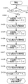
- the flowchart of FIG. 5A shows a process executed by the camera control circuit 101 when the accessory 200 is attached to the camera 100.
- the camera control circuit 101 as a mounting detection means monitors the signal level of the accessory mounting detection signal / ACC_DET and determines whether or not the accessory 200 is mounted. If the signal level is Hi, the camera control circuit 101 returns to S401 and performs detection again, assuming that the accessory 200 is not attached, and if the signal level is Lo, proceeds to S402 assuming that the accessory 200 is attached.
- the camera control circuit 101 sets the power supply control signal CNT_VACC1 to Hi level in order to turn on the output of the accessory power supply circuit A131, and proceeds to S403.
- the accessory power supply circuit A131 outputs the accessory power supply VACC in response to the power supply control signal CNT_VACC1 becoming Hi.
- the camera control circuit 101 monitors the signal level of the overcurrent detection signal DET_OVC and determines whether or not an overcurrent is flowing. If the signal level is Lo, the camera control circuit 101 proceeds to S404 assuming that no overcurrent has flowed, and if the signal level is Hi, proceeds to S405 assuming that an overcurrent has flowed and performs error processing.
- FIG. 6 (a) schematically shows a change in the above signal when the process proceeds to S404 in the process of FIG. 5 (a).
- IACC is the current of the accessory power supply VACC. Since the accessory power supply VACC normally starts up after the power supply control signal CNT_VACC1 is set to Hi in S402, the overcurrent detection signal DET_OVC remains at the Lo level.
- FIG. 6 (b) schematically shows a change in the above signal when the process proceeds to S405 in the process of FIG. 5 (a). Since the overcurrent flows through the IACC after the power supply control signal CNT_VACC1 is set to Hi in S402, the overcurrent detection signal DET_OVC changes to the Hi level and notifies the camera control circuit 101. Upon receiving the notification of the overcurrent detection signal DET_OVC, the camera control circuit 101 turns off the outputs of the accessory power supply circuits A131 and B132 as error processing to stop the power supply to the accessory 200. In this way, even when an overcurrent flows through the accessory power supply VACC, the camera control circuit 101 can detect the overcurrent and safely stop the system.
- the accessory power supply VACC has a voltage of 3.3 V
- the camera microcomputer power supply VMCU_C and the accessory microcomputer power supply VMCU_A have a voltage of 1.8 V. Therefore, if a voltage of 3.3 V is applied to an electric element operating at a voltage of 1.8 V, there is a concern that the electric element may be damaged. Further, since the behavior after the short circuit depends on the characteristics of the electric element, the camera control circuit 101 may not always be able to detect the short circuit between the terminals.
- the I2C communication signal is at the Hi level in the communication standby state, even if it is short-circuited with a 3.3V voltage having a signal voltage of 1.8V or more, an abnormality cannot be detected depending on the characteristics of the connected electric element. In some cases.
- the GND contacts TC04 and TA04 are arranged on one of the two sides of the accessory power supply VACC contacts TC05 and TA05, and the accessory mounting detection signal / ACC_DET contacts TC06 and TA06 are arranged on the other side.
- the accessory mounting detection signal / ACC_DET is connected to the GND in the accessory 200. Therefore, even if a short circuit occurs between the contacts, the overcurrent can be detected and the system can be safely stopped without applying 3.3V to the element operating at 1.8V.
- the accessory power supply VACC is supplied when the GND contact is not connected, the reference potential of the accessory 200 becomes unstable, and as a result, each circuit and the electric element may be damaged. be.
- an external force may be applied that makes the contact of the connector terminals unstable.
- the accessory power supply VACC contact and the GND contact adjacent to each other as in the present embodiment, only the accessory power supply VACC contact is relatively located, rather than arranging the accessory power supply VACC contact and the GND contact at separate terminals. It is possible to make it difficult for the user to be connected.
- the accessory mounting detection signal / ACC_DET is GND-connected in the accessory 200, but as in the accessory 200 shown in FIG. 9, the accessory mounting detection signal / ACC_DET may be GND-connected via the resistance element Rd231. The short-circuit current can be reduced by connecting to GND via the resistor Rd231.
- the voltage (Rd / (Rp + Rd)) ⁇ 1.8V obtained by dividing the voltage of 1.8V of the camera microcomputer power supply VMCU_C by the resistance element Rp134 and the resistance element Rd231 is the Lo level threshold (Vil) of the camera control circuit 101. It is necessary to select a resistance element Rd231 having a resistance value that satisfies the above. For example, when the Low level detection threshold value (Vil) of the camera control circuit 101 is 0.33 times the power supply voltage, the resistance value of the resistance element Rd231 needs to be 1/2 or less of the resistance element Rp134 (10 k ⁇ ). .. In the example of FIG. 9, the resistance value of the resistance element Rd231 is set to 5 k ⁇ .
- FIG. 5B shows a process executed by the camera control circuit 101 when the accessory 200 having the configuration shown in FIG. 9 is attached to the camera 100. Since S411 to S413 are the same as S401 to S403 shown in FIG. 5A, the description thereof will be omitted.
- the camera control circuit 101 monitors the signal level of the accessory mounting detection signal / ACC_DET, and the accessory mounting detection signal / ACC_DET contacts TC06 and TA06 are short-circuited with the accessory power supply VACC contacts TC05 and TA05. Judge whether or not. If the signal level is Lo, the camera control circuit 101 proceeds to S415 as if it is not short-circuited, and if the signal level is Hi, it proceeds to S416 as if it is short-circuited and performs error processing.
- FIG. 6C schematically shows the state of the above signal when the accessory power supply VACC and the accessory mounting detection signal / ACC_DET are short-circuited in the accessory 200 having the configuration of FIG. 9 to which the resistance element Rd231 (5 k ⁇ ) is added. ing. After the power supply control signal CNT_VACC1 is set to Hi in S402, an overcurrent does not flow in the IACC because the current is limited by the resistance element Rd231.
- the voltage of the accessory power supply VACC is applied to the accessory mounting detection signal / ACC_DET.
- the camera control circuit 101 sets the power control signal CNT_VACC1 to Lo as error processing and outputs the accessory power supply VACC (power supply to the accessory 200). Stop it. As a result, the system can be safely stopped without continuously applying 3.3V to the terminals of the element operating at 1.8V.
- the accessory 200 is controlled so that the accessory mounting detection signal / ACC_DET becomes Lo level (GND potential) by the accessory control circuit 201 via an NPN transistor 212 as a switch means. May be.
- the camera control circuit 101 can always detect the accessory 200.
- the accessory control circuit 201 can detect the accessory 200 at an arbitrary timing. It is possible to notify the attachment to the camera.
- the accessory 200 may be configured by connecting the resistance element Rd231 in series with the NPN transistor 212.
- the resistance value needs to be 1/2 or less of the resistance element Rp134 (10 k ⁇ ) as in the configuration of FIG.
- the safety of the system including the camera 100 and the accessory 200 can be maintained, and damage to them can be suppressed. ..
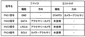
- FIG. 7 shows an example of the functions of the FNC1 signal to the FNC4 signal as the functional signals connected to the contacts TC14 to TC17 and the contacts TA14 to TA17 for each type of the accessory 200 (here, the microphone device and the strobe device). ..
- the FNC2 signal to the FNC4 signal are used as a digital audio (I2S: Inter-IC Sound standard) data bus to transfer audio data.
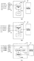
- FIG. 8A shows a configuration example of the functional circuit 206 when the accessory 200 is a microphone device.
- the voice processing circuit 206A1 in the function circuit 206 is a codec circuit that converts a voice signal input from the microphone 206A2 into a digital voice (I2S) data format, and is controlled by the accessory control circuit 201.
- the accessory control circuit 201 can set the sampling frequency and the resolution by controlling the voice processing circuit 206A1. In this embodiment, the sampling frequency is 48 kHz and the resolution is 32 bits.
- the microphone 206A2 is, for example, a MEMS-IC microphone or an electret condenser microphone.
- TA14 is an FNC1 signal that is not used as an I2S data bus and is connected to GND.
- the unused functional signal is connected to GND, but the present invention is not limited to this, and other than the GND potential (0V) such as the power potential and the L level (low potential) or H level (high potential) of the signal. It may be connected to a reference potential which is a stable potential.
- the FNC2 signal connected to the TA15 is an audio data signal (DATA), which is a signal output from the accessory 200 to the camera 100.
- DATA audio data signal
- the FNC3 signal connected to the TA16 is an audio channel clock signal (LRCLK), which is a signal output from the accessory 200 to the camera 100.
- LRCLK audio channel clock signal
- the FNC4 signal connected to the TA17 is an audio bit clock signal (BCLK), which is a signal output from the camera 100 to the accessory 200.
- BCLK audio bit clock signal
- the sampling frequency is 48 kHz and the resolution is 32 bits as described above
- the LRCLK frequency is 48 kHz and the BCLK frequency is 3.072 MHz.
- the maximum frequency of DATA is 1.536 MHz, which is 1/2 cycle of CLK.
- the contact potential is connected to the GND potential, which is the reference potential, next to the contacts TA17 and TC17 to which the FNC4 signal (BCLK) having the highest frequency is connected among the functional signal contacts to which the functional signal is connected.
- Reference potential contacts TA18 and TC18 are arranged.
- the signal wiring to the access interface is generally configured using a flexible substrate. Further, in order to reduce the product cost, the flexible board may have a single-sided specification, and the board wiring is performed in the same arrangement as the contact arrangement.
- the GND contact which is a reference potential contact, is arranged next to the functional signal contact to which the signal having the highest frequency among the functional signals is connected. This makes it possible to suppress radiation noise (EMI) from the functional signal contact, interference with signals connected to other contacts, and crosstalk with signals other than the I2S data bus.
- EMI radiation noise
- the contacts TA17 and TC18 next to the contacts TA17 and TC17 to which the FNC4 signal (BCLK) having the highest frequency is connected are connected to the GND potential which is the reference potential, but the present invention is not limited to GND. The same effect can be obtained even if the connection is made to a stable reference potential other than the potential.
- FIG. 8B is an example showing a configuration in which voice data is increased with respect to FIG. 8A.
- the purpose of increasing audio data is to increase the number of channels and resolution.
- the FNC4 signal connected to the TA17 is an audio bit clock signal (BCLK), which is the same as in FIG. 8A.
- the FNC3 signal connected to the TA14 is an audio channel clock signal (LRCLK), which is a signal output from the accessory 200 to the camera 100.
- LRCLK audio channel clock signal
- the FNC2 signal connected to the TA15 is an audio data signal (DATA2), which is a signal output from the accessory 200 to the camera 100.
- DATA2 audio data signal
- the FNC1 signal connected to the TA16 operates as a voice data signal (DATA2) as a signal output from the accessory 200 to the camera 100.
- DATA2 voice data signal
- the signals with the highest frequency are arranged closer to the GND terminal in order, so that they are relatively relative.
- the configuration can be highly effective in preventing crosstalk.
- FIG. 8C shows a configuration example of the functional circuit 206 when the accessory 200 is a strobe device.
- the light emitting circuit 206B1 in the functional circuit 206 is a strobe light emitting circuit composed of an IGBT, a trigger coil, and the like, and controls light emission of the light emitting unit 206B2.
- the light emitting unit 206B2 is composed of a xenon tube or the like and emits illumination light to irradiate the subject.
- the charging circuit 206B3 is composed of a transformer, a switching FET, a capacitor, and the like, and accumulates electric charges for causing the light emitting unit 206B2 to emit light.
- the FNC1 signal connected to the TA14 is a light emission synchronization signal (STARTX) for controlling the light emission timing of the light emitting unit 206B2, and is a signal output from the camera 100 to the accessory 200.
- the FNC2 signal to FNC4 signal are not used in the strobe device, and no signal is connected to these contacts.
- the unused functional signal contacts are not connected (OPEN), but the present invention is not limited to this, and the power potential and the L level of the signal are adjusted according to the contacts TC15 to TC17 to which the contacts TA15 to TA17 are connected. Alternatively, it may be connected to a stable reference potential such as H level.
- the strobe device only the FNC1 signal is used among the functional signals. Further, although the light emission synchronization signal (STARTX) is not a signal generated periodically, the camera 100 allocates GND to the FNC1 signal when the microphone device is connected so that the configuration of the camera control circuit 101 is not complicated. Can be done.
- the light emission synchronization signal (STARTX) is not a signal generated periodically, the camera 100 allocates GND to the FNC1 signal when the microphone device is connected so that the configuration of the camera control circuit 101 is not complicated. Can be done.
- the SDA (first signal) connected to the contacts TC12 and TA12 as the first signal contact and the SCL (second signal) connected to the contacts TC13 and TA13 as the second signal contact are both I2C communication. It is a signal for. These signals are transmitted by open drain communication. Since both SDA and SCL are pulled up to the camera microcomputer power supply VMCU_C, the signal has a relatively high impedance during communication standby, and is easily affected by crosstalk.
- the communication request signal (fourth signal) / WAKE is assigned to the contacts TC11 and TA11 as the fourth signal contacts next to the SDA contacts TC12 and TA12.
- the communication request signal / WAKE is a signal for making a communication request from the accessory 200 to the camera 100.
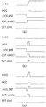
- FIG. 15A shows the timing at which the accessory 200 makes a communication request to the camera 100 and the I2C communication is performed.
- the communication request signal / WAKE is Prior to I2C communication by SCL and SDA, the signal level changes from Hi level to Lo level. This is because I2C communication is performed in response to this change. Therefore, by arranging the communication request signal / WAKE contacts TC11 and TA11 adjacent to the SDA contact and the SDA contact for I2C communication, crosstalk to the communication request signal / WAKE SDA is prevented from occurring. Can be done.
- the communication request signal / WAKE crosses the SDA by controlling the communication request signal / WAKE signal level to be changed from the Lo level to the Hi level after the I2C communication. It is possible to prevent talk from occurring.
- the FNC1 signal is assigned to the contacts TC14 and TA14 as the third signal contact next to the SCL contacts TC13 and TA13. As described above, in the microphone device, since GND is assigned to the FNC1 signal, crosstalk to the SCL can be prevented from occurring.
- FIG. 15B shows the timing at which the accessory 200 makes a communication request to the camera 100, and the I2C communication and the strobe light emission are performed. As shown in FIG. 15B, at the timing (period) when the light emission synchronization signal is output, I2C communication is not performed between the camera 100 and the accessory 200 in order to process the control of the strobe light emission with the highest priority.
- the emission synchronization signal is a signal whose signal level changes before (or after) during I2C communication, but the signal level does not change during I2C communication. This makes it possible to prevent crosstalk of the emission synchronization signal with respect to SCL.
- good I2C communication is enabled by arranging the STARTX contact on one of the sides of the SDA contact and the SCL contact and arranging the / WAKE contact on the other.
- the communication request signal / WAKE connected to the contacts TC11 and TA11 adjacent to the SDA contacts TC12 and TA12 is an open drain type signal like the SDA. Compared with the case where the communication request signal / WAKE is a push-pull system, it is possible to suppress crosstalk to the SDA when the signal level of the communication request signal / WAKE changes.
- the SCLK connected to the SCLK contacts TC07 and TA07 is a clock signal for SPI communication, and operates at a drive frequency of 1 MHz in this embodiment.
- the mounting detection contacts TC06 and TA06 next to the SCLK contacts TC07 and TA07 are used for transmitting the accessory mounting detection signal / ACC_DET.
- the accessory mounting detection signal / ACC_DET is a signal that becomes a potential equivalent to GND when the accessory 200 is mounted on the camera 100. Therefore, by adopting such a contact arrangement, it is possible to prevent crosstalk between SCLK and signals other than the SPI bus.
- the MOSI connected to the contacts TC08 and TA08 next to the SCLK contacts TC07 and TA07 is a data signal transmitted from the camera control circuit 101 to the accessory control circuit 201 by SPI communication.
- the timing at which the MOSI output level in SPI communication changes is synchronized with the timing at which the SCLK output level changes. Therefore, by arranging the MOSI contacts TC08 and TA08 next to the SCLK contacts TC07 and TA07, crosstalk between SCLK and MOSI can be suppressed.
- the MISO connected to the contacts TC09 and TA09 next to the MOSI contacts TC08 and TA08 is a data signal transmitted from the accessory control circuit 201 to the camera control circuit 101 in SPI communication.
- the timing at which the output level of MISO changes in SPI communication is synchronized with the timing at which the output level of SCLK changes, similar to MOSI. Therefore, by arranging the MISO contacts TC09 and TA09 next to the MOSI contacts TC08 and TA08, crosstalk between the MOSI and the MISO can be suppressed.
- the CS connected to the contacts TC10 and TA10 next to the MISO contacts TC09 and TA09 is a communication request signal transmitted from the camera control circuit 101 to the accessory control circuit 201 in SPI communication.
- CS in SPI communication maintains a constant output level from the time when a communication request is made to the time when communication is completed. Therefore, by arranging the CS contacts TC10 and TA10 next to the MISO contacts TC09 and TA09, crosstalk to the MISO can be suppressed.
- the communication request signal / WAKE connected to the contacts TC11 and TA11 adjacent to the CS contacts TC10 and TA10 is a signal for making a communication request from the accessory control circuit 201 to the camera control circuit 101.
- the communication request signal / WAKE is an open drain type signal, it is a signal that is relatively susceptible to crosstalk. Therefore, in the present embodiment, the CS contacts TC10 and TA10, whose signal level changes relatively infrequently, are placed adjacent to the communication request signal / WAKE contacts TC11 and TA11 to crosstalk the communication request signal / WAKE. Can be suppressed.
- both end sides A differential signal that requires impedance control is connected.
- the signal wiring to the access interface is generally configured using a flexible substrate. In order to achieve the desired wiring impedance on a flexible board, it is necessary to keep the distance between the lines of the differential signal and the GND to be wired in parallel, and in the board using both sides, the differential signal It is common to form a mesh-like GND wiring on the back side. As described above, the signal wiring that requires impedance control has relatively large restrictions on the wiring design as compared with a general single-ended signal.
- the differential signal that requires impedance control is connected to the contacts located on both ends of the camera connection portion 141 and the accessory connection portion 211, so that the differential signal is relatively related to other signals. It is lowered to increase the degree of freedom in wiring design.
- the differential signal can be transferred at a high speed of about several hundred Mbps to several Gbps such as USB and PCIe, and is suitable for transferring a large amount of data between devices.
- the differential signal may not be used depending on the type of accessory 200. In such an accessory that does not use a differential signal, the contact assigned to the differential signal is unnecessary, so it is possible to reduce the cost of the accessory by deleting the contact.
- FIG. 12 shows an example in which the configuration of the accessory 200 shown in FIG. 1 is changed. Specifically, it has a configuration in which contacts TA01 to TA03 and TA19 to TA21 and signals and circuits connected to them are omitted. That is, the accessory 200 of FIG. 12 has 15 contacts.
- differential signals are assigned to the contacts TC01 to TC03 and TC19 to TC21 located on both ends of the camera connection portion 141.
- the contact for the differential signal in the accessory connection portion 211 is eliminated, and a contact arrangement including only the contact required for the accessory 200 is adopted.
- the contacts TC04 and TA04 and the contacts TC18 and TA18 near both ends of the camera connection portion 141 and the accessory connection portion 211 are used as GND contacts.
- the contacts at both ends of the accessory connection portion 211 can be made into GND contacts.
- the configuration of the camera 100 and the accessory 200 is as described above.
- the intermediate accessory 300 includes an extension cable for extending the distance between the camera 100 and the accessory 200, an adapter for simultaneously attaching a plurality of accessories to the camera 100, and the like.
- the case where the intermediate accessory 300 is an extension cable will be described.
- the intermediate accessory 300 corresponds to an accessory
- the accessory 200 corresponds to another accessory.
- the intermediate accessory 300 has a camera shoe and an accessory shoe that can be attached to the camera 100 and the accessory 200, respectively, and each of the intermediate accessory 300 is provided with a camera-side intermediate connection portion 311 and an accessory-side intermediate connection portion 312.
- the camera-side intermediate connection portion 311 has 21 contacts TM01 to TM21 arranged in a row, and is a connector for making an electrical connection with the camera 100.
- the contacts TM01 to TM21 each make one-to-one contact with the contacts TC01 to TC21 at the camera connection portion 141.
- the accessory-side intermediate connection portion 312 has 21 contacts TN01 to TN21 arranged in a row, and is a connector for making an electrical connection with the accessory 200.
- the contacts TN01 to TN21 are in one-to-one contact with the contacts TA01 to TA21 in the accessory connection portion 211, respectively.
- the intermediate accessory 300 may receive the power supply from the camera 100, or the power supply from the camera 100 may be transmitted to the accessory 200 as it is.
- the power supply in the present embodiment includes a case where the power supply from the camera 100 is transmitted to the accessory 200 as it is, and the power supply is not supplied to the accessory 300.
- the number of contacts of the camera-side intermediate connection unit 311 is the same as the number of contacts of the camera connection unit 141
- the number of contacts of the accessory-side intermediate connection unit 312 is the same as the number of contacts of the accessory connection unit 211. It is not always necessary to have the same number of each.
- FIG. 14 shows an example in which the configurations of the accessory 200 and the intermediate accessory 300 are changed from the configuration of FIG.
- differential signals are connected to the contacts TC01 to TC03 and TC19 to TC21 on both ends of the camera connection portion 141, the differential signal may not be required depending on the function of the accessory 200.
- the contact points to which the differential signal is connected from the camera side intermediate connection portion 311 and the accessory side intermediate connection portion 312 and the accessory connection portion 211 are eliminated. That is, the intermediate accessory 300 and the accessory 200 in FIG. 14 each have 15 contacts. As a result, a contact arrangement including only the contacts required for the intermediate accessory 300 and the accessory 200 is adopted.
- connection structure between the camera 100 and the external flash unit 120 which is an example of the accessory 200, will be described in detail.
- FIG. 16A shows the camera 100 viewed from the diagonally rear side.
- FIG. 16B shows a method of attaching the external flash unit 120 to the accessory shoe 1123 of the camera 100.
- FIG. 16C shows a state in which the external flash unit 120 is attached to the camera 100 when viewed from the oblique rear side.
- the imaging optical system is provided on the front side (field side) of the camera 100, and the image display unit 107 is provided on the back side of the camera 100.
- a top cover 150 as an exterior member is provided on the upper surface of the camera 100, and an accessory shoe 1123 is arranged with respect to the top cover 150.
- the camera connection portion 206 is provided at the bottom of the external flash unit 120.
- the external flash unit 120 is slid parallel to the front side in the Z direction (mounting side in the first direction) with respect to the camera 100 to engage the camera connection portion 206 and the accessory shoe 1123. Let me. As a result, the external flash unit 120 can be attached to the camera 100.
- the front side in the Z direction is a direction from the back side to the front side of the camera 100, that is, a direction from the image display unit 107 side toward the imaging optical system 122 side.
- the X direction (second direction), the Y direction (third direction), and the Z direction (front-back direction) shown in the drawings after FIG. 16 are common.
- the X direction is a direction orthogonal to the Z direction in the horizontal plane when the Z direction is parallel to the horizontal direction, and is the width direction of the camera 100.
- the Y direction is a direction orthogonal to the Z direction and the X direction, and is the height direction of the camera 100.
- FIG. 17A shows the top cover 150 and the disassembled accessory shoe 1123.
- FIG. 17B shows the assembled accessory shoe 1123.
- the assembly direction of the accessory shoe 1123 with respect to the top cover 150 is the Y direction.
- the accessory shoe 1123 has an engaging member 151, a connection terminal connector 152, a shoe stage 153, and an accessory shoe spring 154.
- the engaging member 151 is a member for holding the external flash unit 120 by engaging with the external flash unit 120.
- the connection terminal connector 152 includes a plurality of connection terminals 152a arranged on the connector base member 152e as a holding member made of a resin material or the like at equal pitches in the X direction and held by the connector base member 152e. ..
- the connection terminal 152a corresponds to the contacts TC01 to TC21 of the camera connection portion 141 shown in FIG.
- connection terminal connector 152 In the connection terminal connector 152, the connection terminal 152a is arranged in the Z direction (front side of the camera 100), which is the mounting direction of the external flash unit 120, as shown in FIG. 17 (b).
- An engagement hole 156 that engages with the lock pin 252 of the external flash unit 120 shown in FIG. 19A is provided behind the connection terminal connector 152 in the Z direction (on the back side of the digital camera 100).
- connection terminal 152a is electrically connected to the external flash unit 120. Further, each of the plurality of connection terminals 152a is electrically connected to the flexible substrate 158 arranged on the lower side of the top cover 150 in the Y direction.
- the flexible substrate 158 is connected to a main substrate (not shown) of the camera 100. Therefore, when the external flash unit 120 is attached to the accessory shoe 1123, communication between the external flash unit 120 and the camera 100 becomes possible.
- the shoe stage 153 is a housing member that surrounds the engaging member 151 and the connection terminal connector 152.
- the accessory shoe holding member 155 is a structural skeleton that holds the engaging member 151. As shown in FIG. 17A, the accessory shoe holding member 155, the flexible substrate 158, the top cover 150, the shoe stage 153, and the connection terminal connector 152 are fastened to the engaging member 151 by four screws 157 for inserting them. Will be done. As a result, these members are positioned and fixed to each other. By arranging four screws 157 one by one in four regions equally divided in the X direction and the Z direction, the members can be connected in a well-balanced manner.
- FIG. 18A shows the structure on the upper surface side of the engaging member 151
- FIG. 18B shows the structure on the lower surface side of the engaging member 151
- FIG. 18C shows the structure of the connection terminal connector 152 on the upper surface side
- FIG. 24 shows the accessory shoe 1123 as viewed from the insertion direction of the external flash unit 120.
- the engaging member 151 is formed by bending a metal plate in a loop shape so that the end faces of the bent end faces face each other at the seam 151a and come into contact with each other.
- the engaging member 151 has a pair of engaging portions 151b and a connecting portion 151c that connects the pair of engaging portions 151b to each other.
- the engaging member 151 is formed with a pair of first screw hole portions 151d used for fastening the screw 157 and a pair of second screw hole portions 151e. Further, the engaging member 151 is formed with an engaging hole portion 156 that engages with the lock pin 252 of the external flash unit 120.
- the pair of engaging portions 151b are separated by a first width (hereinafter, referred to as engagement portion spacing) 151aa in the X direction.
- the holding member 254 of the external flash unit 120 which will be described later, shown in FIG. 19B is inserted into the engaging portion interval 151aa.
- the pair of first screw hole portions 151d are provided at predetermined intervals in the X direction, and the pair of first fastenings provided apart from each other in the X direction at the rear (rear side) in the Z direction. Functions as a hole.
- the pair of second screw hole portions 151e are provided at predetermined intervals in the X direction, and function as a pair of second fastening hole portions provided apart from each other in the X direction in the front in the Z direction. do.
- the engagement hole portion 156 is formed at a position capable of engaging with the lock pin 252 of the external flash unit 120 in the region sandwiched between the pair of first screw hole portions 151d.
- connection terminal connector 152 As shown in FIGS. 17B and 18C, a plurality of connection terminals 152a are exposed.
- the position of the camera connecting portion 206 is determined by the engaging portion spacing 151aa of the engaging member 151. Therefore, the holding member 254 of the external flash unit 120 is positioned with respect to the connection terminal connector 152 by the engaging member 151.
- FIG. 24 shows on both sides of the connection terminal connector 152 (connector base member 152e), which is an example of the camera connection portion 141 shown in FIG. 1, with a plurality of connection terminals 152a sandwiched in the X direction on the front side in the Z direction.
- a contact surface and a groove are formed. That is, an abutting surface 152b that abuts and positions the accessory shoe 1123 in the Z direction when the external flash unit 120 is mounted, and a groove portion 152c into which the accessory shoe 1123 is inserted are formed.
- Each groove portion 152c is formed so as to extend from the contact surface 152b to the front side (mounting side) in the Z direction, and is a slope formed so as to face inward and diagonally upward (inclination with respect to the X direction).
- a portion 152d is provided. The portion of the groove portion 152c above the slope portion 152d extends outward in the X direction from the position of the upper end of the slope portion 152d. This is to prevent a dent (sink) from being generated in the slope portion 152d during resin molding when the slope portion 152d is formed up to the upper end of the groove portion 152c.
- the outermost inner surface 152cc of the groove portion 152c in the connector base member 152e of the accessory shoe 1123 is the inner end surface of the pair of engaging portions 151b of the engaging member 151 (engaging portion spacing 151aa). It is provided on the outer side and inside the outermost inner surface 151bb of the engaging member 151.
- the slope start position 152cc which is the end (lower end) of the slope portion 152d on the bottom surface side of the groove portion 152c, is provided inside the engagement portion spacing 151aa.
- the slope shape starting from the slope start position 152 cc the space into which the shoe device (camera connection portion 206 described later) of the external flash unit 120 is inserted can be expanded, and the degree of freedom in the shape of the shoe device can be secured. It becomes possible.
- the shoe device of the external flash unit 120 can be sufficiently formed with a shape that protects the connection terminals.
- FIG. 19A shows the external flash unit 120 as viewed from the camera connection portion 206 side (lower side in the Y direction).
- FIG. 19B shows the cut surface along the line AA in FIG. 19A and shows the internal structure of the camera connection portion 206.
- FIG. 20A shows the camera connection portion 206. However, the illustration of the base portion 250 and the lock lever 253, which will be described later, is omitted.
- FIG. 20B shows the camera connection portion 206 viewed from the front in the Z direction.
- the camera connecting portion 206 When the camera connecting portion 206 is attached to the accessory shoe 1123 of the camera 100, as shown in FIG. 19B, the camera connecting portion 206 is on the lower side in the Y direction of the base portion 250 of the external flash unit 120 (upper side in FIG. 19A). ).
- the camera connecting portion 206 has a shoe mounting leg (engaging member, shoe plate) 251, a lock pin 252, a lock lever 253, a holding member 254, a connecting plug 256, and a Y-direction holding member 258.
- the shoe mounting leg 251 is an engaging member that engages and holds the external flash unit 120 with the accessory shoe 1123 of the camera 100. That is, the shoe mounting leg 251 is an engaging member on the external flash unit 120 side that can be attached to and detached from the engaging member 151 of the accessory shoe 1123.
- the shoe mounting leg 251 is manufactured by processing a metal plate (sheet metal) in order to secure high mechanical strength against such a large stress.
- the lock pin 252 is a member for preventing the external flash unit 120 from falling off when the camera connecting portion 206 (shoe mounting leg 251) is mounted on the accessory shoe 1123, and the shoe mounting leg 251 is movable in the Y direction. It is held in. Specifically, the lock pin 252 is slidably held in the Y direction by the Y direction holding member 258. The lock lever 253 and the Y-direction holding member 258 are held by the holding member 254.
- the Y-direction holding member 258 is moved downward in the Y-direction in FIG. 19B by a cam portion (not shown).
- the lock pin 252 also moves downward in the Y direction in FIG. 19B together with the holding member 258 in the Y direction.
- the lock pin 252 protrudes from the shoe mounting leg 251 and engages with the engaging hole portion 156 provided in the engaging member 151 of the accessory shoe 1123.
- the lock pin 252 and the engagement hole 156 function as a positioning member in the Z direction for ensuring an electrical connection between the external flash unit 120 and the camera 100.
- connection plug 256 which is an example of the accessory connection portion 211 shown in FIG. 1, is provided on the front side in the Z direction of the camera connection portion 206, is formed of a non-conductive material (dielectric material) such as a resin material, and is a holding member. It is integrated with 254.
- the outermost width T of the connection plug 256 in the X direction is narrower than the width W of the shoe mounting leg 251 in the X direction. As a result, an area for providing the contact portion 251b on the shoe mounting leg 251 is secured.
- the connection plug 256 has a plurality of connection terminals 257 for contacting and communicating with the plurality of connection terminals 152a of the accessory shoe 1123 shown in FIG. 18 (c).
- the connection terminal 257 corresponds to the contacts TA01 to TA21 of the accessory connection portion 211 shown in FIG.
- connection terminals 257 are provided so as to have a one-to-one correspondence with the plurality of connection terminals 152a, and are held by the holding member 254 so as to extend in the Z direction and to line up in the X direction.
- Each connection terminal 257 has a tip portion 257a that comes into contact with the corresponding connection terminal 152a. Further, each connection terminal 257 has a shape extending rearward in the Z direction from the tip portion 257a, and when the tip portion 257a abuts on the connection terminal 152a, the tip portion 257a is elastically deformed to the upper side in the Y direction in FIG. 19 (b). It has an extension portion 257b that is displaced to.
- an extension portion 257c extending upward in the Y direction is formed.
- a flexible substrate connecting portion 257d which is connected to the main substrate (not shown) of the external flash unit 120 and connected to the flexible substrate 259 inserted into the holding member 254 from the upper side in the Y direction is provided. ing.
- the extension portion 257b is formed with a step portion 257e having a step in the Y direction in the middle of the Z direction.
- the stretched portion 257b can be elastically deformed in the Y direction.
- the durability is lowered because a sufficient amount of deformation cannot be obtained, and as a result, the connection terminal 152a and the tip portion 257a are repeatedly attached and detached.
- the stretched portion 257b may be easily damaged. Therefore, by providing the stepped portion 257e on the extending portion 257b, a sufficient distance L is secured without causing the extending portion 257b to interfere with the shoe mounting leg 251.
- connection plugs 256 projecting downward (third direction) in the Y direction so as to sandwich a plurality of connection terminals 257 at both ends in the X direction.
- a protrusion 256a is provided.
- the lower tip portion 256d of each protrusion 256a is a line connecting the lower ends of the tip portion 257a of the connection terminal 257 in order to protect the connection terminal 257 from external forces such as pressure and impact. It protrudes below. That is, the tip portion 257a of the connection terminal 257 is provided above (inside) the line connecting the lower tip portions 256d of the pair of protrusions 256a.
- a slope portion 256b is provided as an outer surface that extends diagonally upward from the lower tip portion 256d and faces diagonally downward, that is, has an inclination with respect to the X direction. Has been done. Since each protrusion 256a has such a shape, the connection plug 256 can be inserted into the groove portion 152c having the slope portion 152d in the connection terminal connector 152.
- the slope portion 256b has a role of releasing external forces such as pressure and impact on the connection plug 256 to prevent the connection plug from being damaged.
- FIG. 20C shows a case where an external force is applied to the connection plug 256 from the X direction.
- FIG. 20 (c) shows the connection plug 256 seen from the front in the Z direction.
- F 1 be the external force from the X direction and define it as a vector.
- the external force F 1 acting on the slope portion 256b is decomposed according to the rules of addition in the vector space, it is decomposed into a component force F 2 in the direction along the slope portion 256b and a component force F 3 in the direction perpendicular to the slope portion 256b. ..
- the component force F 2 and the component force F 3 can be obtained by the following equation (1).
- F 2 F 1 cos ⁇
- F 3 F 1 sin ⁇ (1)
- ⁇ 0 ° ⁇ ⁇ 90 °.
- FIG. 25 shows an enlarged part of the connection plug 256 seen from the Z direction.
- the height from the lower tip portion 256d of the protrusion 256a to the upper surface of the connection plug 256 is B, and from the lower tip portion 256d (slope start position 256c) to the slope portion.
- A be the height of the slope portion 256b to the upper end of 256b.
- A is preferably 1/5 or more of B, and more preferably 1/4 or more, 1/3 or more, or half or more as shown in FIG.
- the slope portion 256b is formed to have a significant dimension for the function of releasing an external force from the X direction, and is generally different from the chamfered shape provided at the corner of the protrusion. Further, the inclination angle ⁇ of the slope portion 256b with respect to the X direction is preferably set in the range of 45 ° ⁇ 20 ° for the above-mentioned function of releasing the external force.
- the slope start position at the lower tip portion 256d of the slope portions 256b on both sides is desirable to make the width between 256c in the X direction as short as possible.
- the width of the slope start position 256c in the X direction is provided inside the width V of the holding member 254 in the X direction, so that the region of the contact portion 251b is sufficiently secured.
- the camera connecting portion 206 has a structure in which the shoe mounting leg 251 and the holding member 254 are fastened. The details of this fastening structure will be described later.
- the holding member 254 can be inserted into the engaging portion spacing 151aa of the engaging member 151 of the accessory shoe 1123 shown in FIG. 18A, and has a width V shorter than the width W of the shoe mounting leg 251 in the X direction. It has a part 254a.
- the width W and width V are defined by Japanese Industrial Standards (JIS) B7101-1975 "Camera accessory mounting seat and mounting foot”.
- the contact portion 251b of the shoe mounting leg 251 comes into contact with the contact surface 152b on the front side in the Z direction of the connection terminal connector 152, so that the position of the external flash unit 120 with respect to the camera 100 is determined in the Z direction.
- the holding member 254 is also a structure for connecting the shoe mounting leg 251 and the base portion 250, and the lock pin 252 and the connecting terminal 257 are arranged inside the connecting portion 254a.
- FIG. 21 (a) shows the camera connection portion 206 seen from the upper side in the Y direction
- FIG. 21 (b) shows the cut surface along the line BB in FIG. 21 (a).
- a pair of first screw 260a and a pair of second screws 260b which are fastening members for fastening the shoe mounting leg 251 to the holding member 254, penetrate the holding member 254 and are fastened to the shoe mounting leg 251.
- the shoe mounting leg 251 is stably held by the holding member 254.
- the shoe mounting leg 251 is a component on which a large stress acts. Therefore, the required mechanical strength is ensured by fastening the metal shoe mounting legs 251 to the holding member 254 with a pair of first screws 260a and a pair of second screws 260b arranged in a well-balanced manner. It will be possible.
- connection terminals 257 are arranged in the region S sandwiched between the pair of first screws 260a and the pair of second screws 260b.
- the width between the pair of first screws 260a and the pair of second screws 260b is the width between the lower tip portion 256d of the protrusion 256a of the connection plug 256, the width V of the holding member 254, and the connection plug. It is narrower than the outermost width T of 256 and the width W of the shoe mounting leg 251.
- FIG. 26 shows a cross section of the accessory shoe 1123 with the camera connection portion 206 attached, as viewed from the Z direction. This figure shows the dimensions T and V of the camera connecting portion 206 and the positional relationship between each portion of the camera connecting portion 206 and each portion of the accessory shoe 1123.
- the upper surface of the shoe fitting portion 251a of the camera connecting portion 206 is in contact with the lower surface (ceiling surface) of the engaging member 151 of the accessory shoe 1123 for positioning in the Y direction.
- the lower tip portion 256d and the slope portion 256b of the protrusion 256a of the connection plug 256 in the camera connecting portion 206 do not abut on the bottom surface and the slope portion 152d of the groove portion 152c of the accessory shoe 1123, respectively.
- the gap between the lower tip portion 256d of the protrusion 256a and the bottom surface of the groove portion 152c of the accessory shoe 1123 is set to be as small as possible.
- the gap between the slope portions 256b and 152d and the gap between the inner end surface 152cc of the groove portion 152c and the outer end surface of the connection plug 256 are set to be large to some extent. As a result, when an external force in the X direction is applied to the external flash unit 120, the connection terminals 257 and 152a can be prevented from being loaded.
- the relationship between the height of the groove portion 152c in the Y direction (the height from the bottom surface of the groove portion 152c to the ceiling surface of the engaging member 151) and the height of the slope portion 152d in the Y direction. Is the same as the relationship between the height B of the connection plug 256 and the height A of the slope portion 256b in the camera connecting portion 206.
- the inclination angle of the slope portion 256b with respect to the X direction is also set in the range of 45 ° ⁇ 20 °, similarly to the inclination angle ⁇ of the slope portion 256b in the camera connecting portion 206.
- the slope portion 256b may be a curved surface having a curvature. That is, the slope portion 256b may be a surface having an inclination with respect to the X direction.
- an area for providing a large number of connection terminals and a shape for protecting them and an area for positioning between parts are secured. be able to.
- FIG. 22A shows the external flash unit 120 as viewed from the camera connection portion 206 side (lower side in the Y direction).
- 22 (b) shows the cut surface along the line AA in FIG. 22 (a), and shows the internal structure of the camera connecting portion 206.
- FIG. 23A shows the camera connection portion 206. However, the illustration of the base portion 250 and the lock lever 253 is omitted.
- FIG. 23B shows the camera connection portion 206 viewed from the front in the Z direction.
- the camera connecting portion 206 When the camera connecting portion 206 is attached to the accessory shoe 1123 of the camera 100, as shown in FIG. 22 (b), the camera connecting portion 206 is on the lower side in the Y direction of the base portion 250 of the external flash unit 120 (upper side in FIG. 22 (a)). ).
- the camera connecting portion 206 has a shoe mounting leg 300a, a lock pin 252, a lock lever 253, a holding member 300, a connecting plug 300b, a Y-direction holding member 258, and a shoe cover 301.
- the shoe mounting leg 300a is an engaging member for engaging the external flash unit 120 with the accessory shoe 1123 of the camera 100, similarly to the shoe mounting leg 251 of the embodiment described above. That is, the shoe mounting leg 300a is an engaging member on the external flash unit 120 side that can be attached to and detached from the engaging member 151 of the accessory shoe 1123.
- the shoe mounting leg 251 which is a metal shoe plate and the resin holding member 254 are formed of separate members in order to give priority to mechanical strength.
- the shoe mounting leg 300a and the holding member 300 are formed as an integral member by a resin material (non-conductive material).
- the pair of first screws 260a and the pair of second screws 260b in the previous embodiment are not required, and the space for arranging the connection terminals 257 becomes wider. Therefore, a larger number of connection terminals 257 are arranged. can do.
- the external flash unit 120 can communicate more information with the camera 100 via the camera connection portion 206 and the accessory shoe 1123.
- connection plug 300b is provided on the front side in the Z direction of the camera connection portion 206, and is formed as an integral member with the holding member 300 formed of a non-conductive resin material in the present embodiment. Similar to the embodiment described above, the outermost width T of the connection plug 300b in the X direction is made narrower than the width W of the shoe mounting leg 300a in the X direction, so that the contact portion 300e is formed in the shoe mounting leg 300a. The area to be provided is secured.
- the connection plug 300b has a plurality of connection terminals 257 for contacting and communicating with the plurality of connection terminals 152a of the accessory shoe 1123 shown in FIG. 18 (c).
- the shoe cover 301 is an enclosure attached to the holding member 300, and is a member that protects a plurality of connection terminals 257.
- the shape of the connection terminal 257 is the same as that of the previous embodiment, and a step portion 257e is provided to secure a sufficient distance L in the Z direction of the extension portion 257b without interfering with the shoe cover 301.
- connection plug 300b is also the same as that of the connection plug 256 of the previous embodiment, and a pair of protrusions protruding downward in the Y direction so as to sandwich a plurality of connection terminals 257 at both ends of the connection plug 300b in the X direction. 300c is provided.
- the lower tip portion 300k of each protrusion 300c is a line connecting the lower ends of the tip portion 257a of the connection terminal 257 in order to protect the connection terminal 257 from external forces such as pressure and impact. It protrudes below. That is, the tip portion 257a of the connection terminal 257 is provided above (inside) the line connecting the lower tip portions 300k of the pair of protrusions 300b.
- a slope portion 300f extending diagonally upward from the lower tip portion 300k and facing diagonally downward side is provided on the outer side of each protrusion 300c in the X direction. Since each protrusion 300c has such a shape, the connection plug 300b can be inserted into the groove 152c having the slope portion 152d in the connection terminal connector 152 described in the previous embodiment. As described in the previous embodiment, the slope portion 300c has a role of releasing an external force such as pressure or impact on the connection plug 300b to prevent the connection plug from being damaged.
- the slope start positions 300g on both sides are provided inside the width V of the holding member 254 in the X direction to sufficiently secure the region of the contact portion 300e of the shoe mounting legs 300a.
- the holding member 300 is formed so that it can be inserted and engaged with the engaging portion spacing 151aa of the engaging member 151 shown in FIG. 18A, and has a width V shorter than the width W of the shoe mounting leg 300a in the X direction. It has a connecting portion 300h.
- the width W and the width V are defined by the Japanese Industrial Standards (JIS) B7101-1975 "Camera accessory mounting seat and mounting foot" as in the previous embodiment.
- the holding member 300 is also a structure for connecting the shoe mounting legs 300a and the base portion 250, and the lock pin 252 and the connecting terminal 257 are arranged inside the connecting portion 300h.
- the case where the camera 100, the accessory 200, and the intermediate accessory 300 have 21 or 15 contacts has been described, but the number of contacts may be other than these.
- the microphone device and the strobe device have been described as the accessory 200, but the accessory referred to in the present invention includes various devices other than the microphone device such as the electronic viewfinder unit and the strobe device.
- the camera has been described as an electronic device, but the electronic device referred to in the present invention also includes various electronic devices other than the camera.
- the present invention supplies a program that realizes one or more functions of the above-described embodiment to a system or device via a network or storage medium, and one or more processors in the computer of the system or device reads and executes the program. It can also be realized by the processing to be performed. It can also be realized by a circuit (for example, ASIC) that realizes one or more functions.
Abstract
Description
SCLおよびSDAによるI2C通信の前に、信号レベルがHiレベルからLoレベルへと変化する。この変化に応じてI2C通信が行われるためである。そこで、通信要求信号/WAKEの接点TC11、TA11を、I2C通信のためのSDA接点およびSDA接点と隣接して配置させることで、通信要求信号/WAKEのSDAに対するクロストークが生じないようにすることができる。
F2=F1cosθ
F3=F1sinθ (1)
斜面部256bを設ける場合は、θは0°<θ<90°となる。この範囲において、
F2<F1
F3<F1 (2)
となる。分力F2は斜面部256bに沿う方向に逃げるため、接続プラグ256に対して影響を及ぼす力は分力F3のみとなる。前述したように、分力F3は分力F1より小さいため、ある程度大きな外力が加わっても接続プラグ256が破損しないようにすることができる。
なお、保持部材300は、シュー取付脚300aと基台部250とを連結するための構造体でもあり、ロックピン252と接続端子257は連結部300hの内部に配置されている。
(その他の実施形態)
本発明は、上述の実施形態の1以上の機能を実現するプログラムを、ネットワーク又は記憶媒体を介してシステム又は装置に供給し、そのシステム又は装置のコンピュータにおける1つ以上のプロセッサーがプログラムを読出し実行する処理でも実現可能である。また、1以上の機能を実現する回路(例えば、ASIC)によっても実現可能である。
Claims (14)
- アクセサリが着脱可能に装着され、前記アクセサリと電気的に接続される複数の接点が一列に配列された電子機器であって、
前記複数の接点は、前記電子機器への前記アクセサリの装着の検出に用いられる装着検出接点と、前記アクセサリから前記電子機器への通信要求に用いられる通信要求接点とを含み、
前記装着検出接点と前記通信要求接点は、前記複数の接点の配列方向における最も一端側の接点と最も他端側の接点との間に配置され、
前記装着検出接点は、前記通信要求接点と前記最も一端側の接点との間に配置されており、
前記配列方向において、前記装着検出接点と前記通信要求接点との間の距離が、前記通信要求接点と前記最も他端側の接点との間の距離よりも短いことを特徴とする電子機器。 - 前記配列方向において、前記通信要求接点と前記最も一端側の接点との間の距離が、前記通信要求接点と前記最も他端側の接点との間の前記距離以下であることを特徴とする請求項1に記載の電子機器。
- 前記配列方向において、前記装着検出接点と前記最も一端側の接点との間の距離が、前記装着検出接点と前記通信要求接点との間の前記距離以上であることを特徴とする請求項1または2に記載の電子機器。
- 前記装着検出接点を介して前記電子機器への前記アクセサリの装着を検出した場合において前記通信要求接点を介して前記通信要求を検出しないときに、エラー処理を行うことを特徴とする請求項1から3のいずれか一項に記載の電子機器。
- 前記装着検出接点と前記通信要求接点との間および前記通信要求接点に対して前記装着検出接点とは反対側にそれぞれ、前記電子機器と前記アクセサリとの間の通信に用いられる通信接点が配置されていることを特徴とする請求項1から4のいずれか一項に記載の電子機器。
- 前記電子機器は、前記アクセサリとの間で、第1の通信方式での通信と該第1の通信方式とは異なる第2の通信方式での通信とが可能であり、
前記通信要求接点に対して前記装着検出接点とは反対側に、前記第1の通信方式での通信に用いられる通信接点が配置され、
前記通信要求接点と前記装着検出接点との間に、前記第2の通信方式での通信に用いられる通信接点が配置されていることを特徴とする請求項5に記載の電子機器。 - 請求項1から6のいずれか一項に記載の電子機器と、
該電子機器に着脱可能に装着されるアクセサリとを有することを特徴とするシステム。 - 電子機器に着脱可能に装着され、前記電子機器と電気的に接続される複数の接点が一列に配列されたアクセサリであって、
前記複数の接点は、前記電子機器への前記アクセサリの装着の検出に用いられる装着検出接点と、前記アクセサリから前記電子機器への通信要求に用いられる通信要求接点とを含み、
前記装着検出接点と前記通信要求接点は、前記複数の接点の配列方向における最も一端側の接点と最も他端側の接点との間に配置され、
前記装着検出接点は、前記通信要求接点と前記最も一端側の接点との間に配置されており、
前記配列方向において、前記装着検出接点と前記通信要求接点との間の距離が、前記通信要求接点と前記最も他端側の接点との間の距離よりも短いことを特徴とするアクセサリ。 - 前記配列方向において、前記通信要求接点と前記最も一端側の接点との間の距離が、前記通信要求接点と前記最も他端側の接点との間の前記距離以下であることを特徴とする請求項8に記載のアクセサリ。
- 前記配列方向において、前記装着検出接点と前記最も一端側の接点との間の距離が、前記装着検出接点と前記通信要求接点との間の前記距離以上であることを特徴とする請求項8または9に記載のアクセサリ。
- 前記複数の接点が、前記電子機器に設けられた複数の接点への接触方向に向かって凸形状を有する保持部材により保持されていることを特徴とする請求項8から10のいずれか一項に記載のアクセサリ。
- 前記装着検出接点と前記通信要求接点との間および前記通信要求接点に対して前記装着検出接点とは反対側にそれぞれ、前記電子機器と前記アクセサリとの間の通信に用いられる通信接点が配置されていることを特徴とする請求項7から10のいずれか一項に記載のアクセサリ。
- 前記アクセサリは、前記電子機器との間で、第1の通信方式での通信と該第1の通信方式とは異なる第2の通信方式での通信とが可能であり、
前記通信要求接点に対して前記装着検出接点とは反対側に、前記第1の通信方式での通信に用いられる接点が配置され、
前記通信要求接点と前記装着検出接点との間に、前記第2の通信方式での通信に用いられる接点が配置されていることを特徴とする請求項12に記載のアクセサリ。 - 電子機器と、
該電子機器に着脱可能に装着される請求項8から13のいずれか一項に記載のアクセサリとを有することを特徴とするシステム。
Priority Applications (6)
| Application Number | Priority Date | Filing Date | Title |
|---|---|---|---|
| CN202180003706.1A CN113906341B (zh) | 2020-04-09 | 2021-04-02 | 电子设备和配件 |
| CN202410030245.2A CN117850125A (zh) | 2020-04-09 | 2021-04-02 | 电子设备和配件 |
| BR112021021885A BR112021021885A2 (pt) | 2020-04-09 | 2021-04-02 | Aparelho eletrônico e acessório |
| EP21785644.2A EP4024128A4 (en) | 2020-04-09 | 2021-04-02 | ELECTRONIC DEVICE AND ACCESSORY |
| US17/533,904 US11886099B2 (en) | 2020-04-09 | 2021-11-23 | Electronic apparatus and accessory |
| US18/514,042 US20240085764A1 (en) | 2020-04-09 | 2023-11-20 | Electronic apparatus and accessory |
Applications Claiming Priority (8)
| Application Number | Priority Date | Filing Date | Title |
|---|---|---|---|
| JP2020-070626 | 2020-04-09 | ||
| JP2020-070627 | 2020-04-09 | ||
| JP2020070627 | 2020-04-09 | ||
| JP2020070626 | 2020-04-09 | ||
| JP2020070625 | 2020-04-09 | ||
| JP2020-070625 | 2020-04-09 | ||
| JP2021-060601 | 2021-03-31 | ||
| JP2021060601A JP7087152B2 (ja) | 2020-04-09 | 2021-03-31 | 電子機器およびアクセサリ |
Related Child Applications (1)
| Application Number | Title | Priority Date | Filing Date |
|---|---|---|---|
| US17/533,904 Continuation US11886099B2 (en) | 2020-04-09 | 2021-11-23 | Electronic apparatus and accessory |
Publications (1)
| Publication Number | Publication Date |
|---|---|
| WO2021206009A1 true WO2021206009A1 (ja) | 2021-10-14 |
Family
ID=78023245
Family Applications (1)
| Application Number | Title | Priority Date | Filing Date |
|---|---|---|---|
| PCT/JP2021/014288 WO2021206009A1 (ja) | 2020-04-09 | 2021-04-02 | 電子機器およびアクセサリ |
Country Status (6)
| Country | Link |
|---|---|
| US (2) | US11886099B2 (ja) |
| EP (1) | EP4024128A4 (ja) |
| JP (1) | JP2022118055A (ja) |
| CN (2) | CN117850125A (ja) |
| BR (1) | BR112021021885A2 (ja) |
| WO (1) | WO2021206009A1 (ja) |
Citations (4)
| Publication number | Priority date | Publication date | Assignee | Title |
|---|---|---|---|---|
| JP2012189980A (ja) * | 2011-02-25 | 2012-10-04 | Nikon Corp | アクセサリー、カメラボディおよびカメラシステム |
| JP2013034172A (ja) | 2011-06-30 | 2013-02-14 | Nikon Corp | アクセサリー、カメラ、アクセサリーシュー、及びコネクター |
| JP2013048404A (ja) * | 2011-07-22 | 2013-03-07 | Nikon Corp | カメラシステム、アクセサリー、カメラ、カメラシステム制御プログラム、アクセサリー制御プログラム、及びカメラ制御プログラム |
| JP2020024378A (ja) * | 2018-06-29 | 2020-02-13 | キヤノン株式会社 | 撮像装置、アクセサリ装置およびそれらの通信制御方法 |
Family Cites Families (58)
| Publication number | Priority date | Publication date | Assignee | Title |
|---|---|---|---|---|
| US4887120A (en) | 1984-02-04 | 1989-12-12 | Ricoh Company, Ltd. | Electronic flash photographing system |
| US5384611A (en) | 1991-05-20 | 1995-01-24 | Minolta Camera Kabushiki Kaisha | Camera system capable of wireless flash photographing |
| JP2769524B2 (ja) | 1994-05-09 | 1998-06-25 | 株式会社ニコン | 交換レンズ及びカメラシステム |
| JPH09185103A (ja) | 1996-01-05 | 1997-07-15 | Nikon Corp | 電子機器用コネクタおよび光学システム |
| JP3685908B2 (ja) | 1997-05-30 | 2005-08-24 | 富士通コンポーネント株式会社 | 高速伝送用コネクタ |
| JP2000184264A (ja) * | 1998-12-14 | 2000-06-30 | Olympus Optical Co Ltd | カメラ |
| US7612826B2 (en) | 2004-04-27 | 2009-11-03 | Sony Corporation | Electronic device and accessory device |
| JP4375268B2 (ja) | 2004-04-27 | 2009-12-02 | ソニー株式会社 | 電子機器およびアクセサリー機器 |
| JP2006064763A (ja) * | 2004-08-24 | 2006-03-09 | Sony Corp | 撮像装置及びその設定変更方法 |
| JP4392363B2 (ja) | 2005-02-14 | 2009-12-24 | 富士フイルム株式会社 | カメラ |
| US7331802B2 (en) | 2005-11-02 | 2008-02-19 | Tyco Electronics Corporation | Orthogonal connector |
| JP5275564B2 (ja) | 2006-12-22 | 2013-08-28 | 本田技研工業株式会社 | 燃料電池スタック |
| JP4527140B2 (ja) | 2007-08-07 | 2010-08-18 | 日立オートモティブシステムズ株式会社 | 車載カメラ装置 |
| JP5247859B2 (ja) | 2010-10-27 | 2013-07-24 | キヤノン株式会社 | 撮像装置及びその制御方法、アクセサリ及びその制御方法、撮像装置システム |
| KR101780022B1 (ko) | 2011-01-25 | 2017-09-19 | 삼성전자주식회사 | 카메라 플래시용 어댑터 |
| JP5445479B2 (ja) | 2011-01-28 | 2014-03-19 | 株式会社ニコン | カメラ用アクセサリ、アクセサリ側マウント、カメラボディおよびボディ側マウント |
| CN102854711A (zh) | 2011-06-30 | 2013-01-02 | 株式会社尼康 | 附件、相机、附件插座、及连接器 |
| JP5556842B2 (ja) | 2011-06-30 | 2014-07-23 | 株式会社ニコン | アクセサリー、カメラ、アクセサリーシュー、及びコネクター |
| JP5310899B2 (ja) | 2011-06-30 | 2013-10-09 | 株式会社ニコン | アクセサリー、カメラ、アクセサリーシュー、及びコネクター |
| US20130028586A1 (en) * | 2011-07-22 | 2013-01-31 | Nikon Corporation | Camera system, accessory, camera, camera system control program, accessory control program, and camera control program |
| US8755684B2 (en) | 2011-07-22 | 2014-06-17 | Nikon Corporation | Adapter, camera system, and adapter control program |
| JP5862148B2 (ja) | 2011-07-25 | 2016-02-16 | 株式会社ニコン | カメラボディ、カメラシステム、および、プログラム |
| JP5894397B2 (ja) | 2011-08-29 | 2016-03-30 | キヤノン株式会社 | 撮像装置、アクセサリ及び撮像システム |
| TWI468840B (zh) | 2012-02-28 | 2015-01-11 | Canon Kk | 可裝卸地安裝到相機側配件插座的相機配件裝置 |
| JP5955136B2 (ja) | 2012-07-05 | 2016-07-20 | キヤノン株式会社 | カメラアクセサリおよびカメラ |
| EP3543786B1 (en) | 2012-04-04 | 2022-05-18 | Canon Kabushiki Kaisha | Camera and camera accessory |
| RU2655042C1 (ru) | 2012-04-04 | 2018-05-23 | Кэнон Кабусики Кайся | Камера и комплектующая к камере |
| WO2013168742A1 (ja) | 2012-05-08 | 2013-11-14 | 株式会社ニコン | アクセサリ,カメラボディ |
| JP5996286B2 (ja) * | 2012-06-12 | 2016-09-21 | オリンパス株式会社 | 外部ストロボ装置および撮像装置 |
| JP5701267B2 (ja) | 2012-07-20 | 2015-04-15 | キヤノン株式会社 | カメラおよびカメラアクセサリ |
| JP2015023076A (ja) | 2013-07-17 | 2015-02-02 | 船井電機株式会社 | 信号線のシールド構造、及び、信号伝送方法 |
| JP3187195U (ja) | 2013-09-03 | 2013-11-14 | ティアック株式会社 | カメラシュー延長装置 |
| JP2015075503A (ja) | 2013-10-04 | 2015-04-20 | 株式会社ニコン | 表示用アクセサリ |
| CN105637399B (zh) | 2013-10-09 | 2017-12-22 | 夏普株式会社 | 摄像机模块和摄像机模块的制造方法 |
| WO2015068492A1 (ja) * | 2013-11-08 | 2015-05-14 | 富士フイルム株式会社 | カメラシステム、カメラ本体、交換レンズ及び通信方法 |
| US9571151B2 (en) | 2014-02-06 | 2017-02-14 | Olloclip, Llc | Cases for mobile electronic devices configured to receive auxiliary optical devices |
| JP2016166967A (ja) | 2015-03-10 | 2016-09-15 | キヤノン株式会社 | カメラシステム |
| US9703173B2 (en) | 2015-04-21 | 2017-07-11 | Apple Inc. | Camera module structure having electronic device connections formed therein |
| JP6584129B2 (ja) * | 2015-05-07 | 2019-10-02 | キヤノン株式会社 | 照明装置 |
| DE112016004987T5 (de) * | 2015-10-30 | 2018-07-19 | Canon Kabushiki Kaisha | Elektronische vorrichtung |
| WO2017073081A1 (ja) | 2015-10-30 | 2017-05-04 | キヤノン株式会社 | 電子機器 |
| JP6716271B2 (ja) | 2016-02-03 | 2020-07-01 | キヤノン株式会社 | アクセサリ用信号端子コネクタ、アクセサリーシュー装置、及び撮像装置並びにアクセサリ |
| JP6918470B2 (ja) | 2016-11-24 | 2021-08-11 | キヤノン株式会社 | アクセサリシュー装置、撮像装置、及びアクセサリ |
| US9985399B2 (en) | 2016-02-03 | 2018-05-29 | Canon Kabushiki Kaisha | Accessory shoe device to which accessory is attached, image pickup apparatus, and accessory |
| JP2017151161A (ja) | 2016-02-22 | 2017-08-31 | 株式会社ニコン | アクセサリおよび撮像装置 |
| JP2017151160A (ja) * | 2016-02-22 | 2017-08-31 | 株式会社ニコン | アクセサリおよび撮像装置 |
| RU2724459C2 (ru) | 2017-05-31 | 2020-06-23 | Кэнон Кабусики Кайся | Устройство объектива, устройство захвата изображений, на котором может устанавливаться устройство объектива, и система камеры |
| TWI681245B (zh) | 2017-05-31 | 2020-01-01 | 日商佳能股份有限公司 | 安裝設備及用於成像設備的配件 |
| TWI776256B (zh) | 2017-05-31 | 2022-09-01 | 日商佳能股份有限公司 | 安裝件設備和配件 |
| RU2714847C2 (ru) | 2017-05-31 | 2020-02-19 | Кэнон Кабусики Кайся | Устройство захвата изображения и аксессуары |
| JP2018207427A (ja) | 2017-06-09 | 2018-12-27 | キヤノン株式会社 | 撮像装置 |
| JP6918594B2 (ja) | 2017-06-22 | 2021-08-11 | キヤノン株式会社 | 撮像装置 |
| JP2019078933A (ja) | 2017-10-26 | 2019-05-23 | 株式会社ニコン | アクセサリ |
| JP6455577B1 (ja) | 2017-10-26 | 2019-01-23 | 株式会社ニコン | アクセサリ |
| CN110661964A (zh) * | 2018-06-28 | 2020-01-07 | 佳能株式会社 | 摄像设备、配件设备及其通信控制方法和存储介质 |
| US11412125B2 (en) | 2018-06-29 | 2022-08-09 | Canon Kabushiki Kaisha | Imaging apparatus, accessory apparatus, and communication control method |
| JP7327915B2 (ja) | 2018-08-30 | 2023-08-16 | キヤノン株式会社 | 撮像装置 |
| JP7099303B2 (ja) * | 2018-12-19 | 2022-07-12 | 株式会社ニコン | アクセサリ、カメラボディ及び電子機器 |
-
2021
- 2021-04-02 CN CN202410030245.2A patent/CN117850125A/zh active Pending
- 2021-04-02 WO PCT/JP2021/014288 patent/WO2021206009A1/ja unknown
- 2021-04-02 CN CN202180003706.1A patent/CN113906341B/zh active Active
- 2021-04-02 BR BR112021021885A patent/BR112021021885A2/pt unknown
- 2021-04-02 EP EP21785644.2A patent/EP4024128A4/en active Pending
- 2021-11-23 US US17/533,904 patent/US11886099B2/en active Active
-
2022
- 2022-06-08 JP JP2022092840A patent/JP2022118055A/ja active Pending
-
2023
- 2023-11-20 US US18/514,042 patent/US20240085764A1/en active Pending
Patent Citations (4)
| Publication number | Priority date | Publication date | Assignee | Title |
|---|---|---|---|---|
| JP2012189980A (ja) * | 2011-02-25 | 2012-10-04 | Nikon Corp | アクセサリー、カメラボディおよびカメラシステム |
| JP2013034172A (ja) | 2011-06-30 | 2013-02-14 | Nikon Corp | アクセサリー、カメラ、アクセサリーシュー、及びコネクター |
| JP2013048404A (ja) * | 2011-07-22 | 2013-03-07 | Nikon Corp | カメラシステム、アクセサリー、カメラ、カメラシステム制御プログラム、アクセサリー制御プログラム、及びカメラ制御プログラム |
| JP2020024378A (ja) * | 2018-06-29 | 2020-02-13 | キヤノン株式会社 | 撮像装置、アクセサリ装置およびそれらの通信制御方法 |
Non-Patent Citations (1)
| Title |
|---|
| See also references of EP4024128A4 |
Also Published As
| Publication number | Publication date |
|---|---|
| CN113906341A (zh) | 2022-01-07 |
| JP2022118055A (ja) | 2022-08-12 |
| CN113906341B (zh) | 2024-01-09 |
| EP4024128A4 (en) | 2024-02-21 |
| CN117850125A (zh) | 2024-04-09 |
| US20220082905A1 (en) | 2022-03-17 |
| EP4024128A1 (en) | 2022-07-06 |
| US20240085764A1 (en) | 2024-03-14 |
| TW202210925A (zh) | 2022-03-16 |
| BR112021021885A2 (pt) | 2022-12-06 |
| US11886099B2 (en) | 2024-01-30 |
Similar Documents
| Publication | Publication Date | Title |
|---|---|---|
| US20230400754A1 (en) | Electronic apparatus and accessory | |
| WO2021206006A1 (ja) | 電子機器およびアクセサリ | |
| CN217692026U (zh) | 插座设备、配件、配件插座设备和电子设备 | |
| WO2021206009A1 (ja) | 電子機器およびアクセサリ | |
| WO2021206000A1 (ja) | 電子機器およびアクセサリ | |
| WO2021205998A1 (ja) | 電子機器およびアクセサリ | |
| JP7005804B2 (ja) | 電子機器およびアクセサリ | |
| WO2021205999A1 (ja) | 電子機器およびアクセサリ | |
| TWI837465B (zh) | 照相機之電子機器、系統及配件 |
Legal Events
| Date | Code | Title | Description |
|---|---|---|---|
| REG | Reference to national code |
Ref country code: BR Ref legal event code: B01A Ref document number: 112021021885 Country of ref document: BR |
|
| 121 | Ep: the epo has been informed by wipo that ep was designated in this application |
Ref document number: 21785644 Country of ref document: EP Kind code of ref document: A1 |
|
| ENP | Entry into the national phase |
Ref document number: 2021785644 Country of ref document: EP Effective date: 20220329 |
|
| NENP | Non-entry into the national phase |
Ref country code: DE |
|
| ENP | Entry into the national phase |
Ref document number: 112021021885 Country of ref document: BR Kind code of ref document: A2 Effective date: 20211029 |