WO2021201235A1 - 半導体装置および半導体装置の製造方法 - Google Patents
半導体装置および半導体装置の製造方法 Download PDFInfo
- Publication number
- WO2021201235A1 WO2021201235A1 PCT/JP2021/014179 JP2021014179W WO2021201235A1 WO 2021201235 A1 WO2021201235 A1 WO 2021201235A1 JP 2021014179 W JP2021014179 W JP 2021014179W WO 2021201235 A1 WO2021201235 A1 WO 2021201235A1
- Authority
- WO
- WIPO (PCT)
- Prior art keywords
- concentration
- region
- donor
- semiconductor substrate
- peak
- Prior art date
Links
- 239000004065 semiconductor Substances 0.000 title claims abstract description 263
- 238000000034 method Methods 0.000 title claims description 36
- 238000004519 manufacturing process Methods 0.000 title claims description 23
- 239000000386 donor Substances 0.000 claims abstract description 247
- 239000000758 substrate Substances 0.000 claims abstract description 185
- 238000009826 distribution Methods 0.000 claims abstract description 52
- 239000000852 hydrogen donor Substances 0.000 claims abstract description 43
- 229910052739 hydrogen Inorganic materials 0.000 claims description 170
- 239000001257 hydrogen Substances 0.000 claims description 170
- 239000000126 substance Substances 0.000 claims description 161
- UFHFLCQGNIYNRP-UHFFFAOYSA-N Hydrogen Chemical compound [H][H] UFHFLCQGNIYNRP-UHFFFAOYSA-N 0.000 claims description 133
- 239000012535 impurity Substances 0.000 claims description 65
- 239000002245 particle Substances 0.000 claims description 42
- 238000000137 annealing Methods 0.000 claims description 32
- -1 hydrogen ions Chemical class 0.000 claims description 31
- 239000002019 doping agent Substances 0.000 claims description 28
- 238000002347 injection Methods 0.000 claims description 28
- 239000007924 injection Substances 0.000 claims description 28
- 230000007423 decrease Effects 0.000 claims description 13
- 230000003247 decreasing effect Effects 0.000 claims 1
- 230000007547 defect Effects 0.000 description 69
- 239000000370 acceptor Substances 0.000 description 28
- 238000010586 diagram Methods 0.000 description 20
- OAICVXFJPJFONN-UHFFFAOYSA-N Phosphorus Chemical compound [P] OAICVXFJPJFONN-UHFFFAOYSA-N 0.000 description 19
- 229910052698 phosphorus Inorganic materials 0.000 description 19
- 239000011574 phosphorus Substances 0.000 description 19
- 239000011229 interlayer Substances 0.000 description 15
- 230000002093 peripheral effect Effects 0.000 description 13
- 238000003860 storage Methods 0.000 description 13
- 239000010410 layer Substances 0.000 description 12
- 238000009825 accumulation Methods 0.000 description 8
- 238000009792 diffusion process Methods 0.000 description 8
- QVGXLLKOCUKJST-UHFFFAOYSA-N atomic oxygen Chemical compound [O] QVGXLLKOCUKJST-UHFFFAOYSA-N 0.000 description 7
- 229910052751 metal Inorganic materials 0.000 description 7
- 239000002184 metal Substances 0.000 description 7
- 229910052760 oxygen Inorganic materials 0.000 description 7
- 239000001301 oxygen Substances 0.000 description 7
- 230000004913 activation Effects 0.000 description 6
- 229910052782 aluminium Inorganic materials 0.000 description 6
- XAGFODPZIPBFFR-UHFFFAOYSA-N aluminium Chemical compound [Al] XAGFODPZIPBFFR-UHFFFAOYSA-N 0.000 description 6
- 229910052734 helium Inorganic materials 0.000 description 6
- 239000001307 helium Substances 0.000 description 6
- XUIMIQQOPSSXEZ-UHFFFAOYSA-N Silicon Chemical compound [Si] XUIMIQQOPSSXEZ-UHFFFAOYSA-N 0.000 description 5
- 150000002431 hydrogen Chemical class 0.000 description 5
- 239000011148 porous material Substances 0.000 description 5
- 229910052710 silicon Inorganic materials 0.000 description 5
- 239000010703 silicon Substances 0.000 description 5
- 125000004429 atom Chemical group 0.000 description 4
- 230000005684 electric field Effects 0.000 description 4
- SWQJXJOGLNCZEY-UHFFFAOYSA-N helium atom Chemical compound [He] SWQJXJOGLNCZEY-UHFFFAOYSA-N 0.000 description 4
- 150000002500 ions Chemical class 0.000 description 4
- 229910021420 polycrystalline silicon Inorganic materials 0.000 description 4
- 229920005591 polysilicon Polymers 0.000 description 4
- ZOXJGFHDIHLPTG-UHFFFAOYSA-N Boron Chemical compound [B] ZOXJGFHDIHLPTG-UHFFFAOYSA-N 0.000 description 3
- 230000001133 acceleration Effects 0.000 description 3
- 229910052785 arsenic Inorganic materials 0.000 description 3
- RQNWIZPPADIBDY-UHFFFAOYSA-N arsenic atom Chemical compound [As] RQNWIZPPADIBDY-UHFFFAOYSA-N 0.000 description 3
- 230000015572 biosynthetic process Effects 0.000 description 3
- 229910052796 boron Inorganic materials 0.000 description 3
- 230000000052 comparative effect Effects 0.000 description 3
- 125000004435 hydrogen atom Chemical group [H]* 0.000 description 3
- 239000000463 material Substances 0.000 description 3
- 230000008569 process Effects 0.000 description 3
- 238000013459 approach Methods 0.000 description 2
- 230000004888 barrier function Effects 0.000 description 2
- 239000004020 conductor Substances 0.000 description 2
- 238000001514 detection method Methods 0.000 description 2
- 230000001747 exhibiting effect Effects 0.000 description 2
- GPRLSGONYQIRFK-UHFFFAOYSA-N hydron Chemical compound [H+] GPRLSGONYQIRFK-UHFFFAOYSA-N 0.000 description 2
- 238000005259 measurement Methods 0.000 description 2
- 238000000691 measurement method Methods 0.000 description 2
- 239000007769 metal material Substances 0.000 description 2
- 238000001004 secondary ion mass spectrometry Methods 0.000 description 2
- 229910052711 selenium Inorganic materials 0.000 description 2
- 239000011669 selenium Substances 0.000 description 2
- 238000003892 spreading Methods 0.000 description 2
- 230000007480 spreading Effects 0.000 description 2
- 229910000789 Aluminium-silicon alloy Inorganic materials 0.000 description 1
- 229910019142 PO4 Inorganic materials 0.000 description 1
- BUGBHKTXTAQXES-UHFFFAOYSA-N Selenium Chemical compound [Se] BUGBHKTXTAQXES-UHFFFAOYSA-N 0.000 description 1
- 229910000676 Si alloy Inorganic materials 0.000 description 1
- NINIDFKCEFEMDL-UHFFFAOYSA-N Sulfur Chemical compound [S] NINIDFKCEFEMDL-UHFFFAOYSA-N 0.000 description 1
- RTAQQCXQSZGOHL-UHFFFAOYSA-N Titanium Chemical compound [Ti] RTAQQCXQSZGOHL-UHFFFAOYSA-N 0.000 description 1
- KPSZQYZCNSCYGG-UHFFFAOYSA-N [B].[B] Chemical compound [B].[B] KPSZQYZCNSCYGG-UHFFFAOYSA-N 0.000 description 1
- CSDREXVUYHZDNP-UHFFFAOYSA-N alumanylidynesilicon Chemical compound [Al].[Si] CSDREXVUYHZDNP-UHFFFAOYSA-N 0.000 description 1
- 229910052787 antimony Inorganic materials 0.000 description 1
- WATWJIUSRGPENY-UHFFFAOYSA-N antimony atom Chemical compound [Sb] WATWJIUSRGPENY-UHFFFAOYSA-N 0.000 description 1
- 239000000969 carrier Substances 0.000 description 1
- 230000008859 change Effects 0.000 description 1
- 239000013078 crystal Substances 0.000 description 1
- 230000000694 effects Effects 0.000 description 1
- 238000010894 electron beam technology Methods 0.000 description 1
- 230000005484 gravity Effects 0.000 description 1
- 238000005468 ion implantation Methods 0.000 description 1
- 229910001092 metal group alloy Inorganic materials 0.000 description 1
- 238000012986 modification Methods 0.000 description 1
- 230000004048 modification Effects 0.000 description 1
- 238000005121 nitriding Methods 0.000 description 1
- 238000010606 normalization Methods 0.000 description 1
- 230000001590 oxidative effect Effects 0.000 description 1
- 230000035515 penetration Effects 0.000 description 1
- NBIIXXVUZAFLBC-UHFFFAOYSA-K phosphate Chemical compound [O-]P([O-])([O-])=O NBIIXXVUZAFLBC-UHFFFAOYSA-K 0.000 description 1
- 239000010452 phosphate Substances 0.000 description 1
- 230000001737 promoting effect Effects 0.000 description 1
- 125000003748 selenium group Chemical group *[Se]* 0.000 description 1
- 239000005368 silicate glass Substances 0.000 description 1
- 229910052717 sulfur Inorganic materials 0.000 description 1
- 239000011593 sulfur Substances 0.000 description 1
- 239000002344 surface layer Substances 0.000 description 1
- 230000036413 temperature sense Effects 0.000 description 1
- 239000010936 titanium Substances 0.000 description 1
- 229910052719 titanium Inorganic materials 0.000 description 1
- 150000003609 titanium compounds Chemical class 0.000 description 1
- 238000012546 transfer Methods 0.000 description 1
- WFKWXMTUELFFGS-UHFFFAOYSA-N tungsten Chemical compound [W] WFKWXMTUELFFGS-UHFFFAOYSA-N 0.000 description 1
- 229910052721 tungsten Inorganic materials 0.000 description 1
- 239000010937 tungsten Substances 0.000 description 1
Images


Classifications
-
- H—ELECTRICITY
- H01—ELECTRIC ELEMENTS
- H01L—SEMICONDUCTOR DEVICES NOT COVERED BY CLASS H10
- H01L29/00—Semiconductor devices specially adapted for rectifying, amplifying, oscillating or switching and having potential barriers; Capacitors or resistors having potential barriers, e.g. a PN-junction depletion layer or carrier concentration layer; Details of semiconductor bodies or of electrodes thereof ; Multistep manufacturing processes therefor
- H01L29/66—Types of semiconductor device ; Multistep manufacturing processes therefor
- H01L29/68—Types of semiconductor device ; Multistep manufacturing processes therefor controllable by only the electric current supplied, or only the electric potential applied, to an electrode which does not carry the current to be rectified, amplified or switched
- H01L29/70—Bipolar devices
- H01L29/72—Transistor-type devices, i.e. able to continuously respond to applied control signals
- H01L29/739—Transistor-type devices, i.e. able to continuously respond to applied control signals controlled by field-effect, e.g. bipolar static induction transistors [BSIT]
-
- H—ELECTRICITY
- H01—ELECTRIC ELEMENTS
- H01L—SEMICONDUCTOR DEVICES NOT COVERED BY CLASS H10
- H01L21/00—Processes or apparatus adapted for the manufacture or treatment of semiconductor or solid state devices or of parts thereof
- H01L21/02—Manufacture or treatment of semiconductor devices or of parts thereof
- H01L21/04—Manufacture or treatment of semiconductor devices or of parts thereof the devices having potential barriers, e.g. a PN junction, depletion layer or carrier concentration layer
- H01L21/18—Manufacture or treatment of semiconductor devices or of parts thereof the devices having potential barriers, e.g. a PN junction, depletion layer or carrier concentration layer the devices having semiconductor bodies comprising elements of Group IV of the Periodic Table or AIIIBV compounds with or without impurities, e.g. doping materials
- H01L21/22—Diffusion of impurity materials, e.g. doping materials, electrode materials, into or out of a semiconductor body, or between semiconductor regions; Interactions between two or more impurities; Redistribution of impurities
- H01L21/221—Diffusion of impurity materials, e.g. doping materials, electrode materials, into or out of a semiconductor body, or between semiconductor regions; Interactions between two or more impurities; Redistribution of impurities of killers
-
- H—ELECTRICITY
- H01—ELECTRIC ELEMENTS
- H01L—SEMICONDUCTOR DEVICES NOT COVERED BY CLASS H10
- H01L29/00—Semiconductor devices specially adapted for rectifying, amplifying, oscillating or switching and having potential barriers; Capacitors or resistors having potential barriers, e.g. a PN-junction depletion layer or carrier concentration layer; Details of semiconductor bodies or of electrodes thereof ; Multistep manufacturing processes therefor
- H01L29/66—Types of semiconductor device ; Multistep manufacturing processes therefor
- H01L29/86—Types of semiconductor device ; Multistep manufacturing processes therefor controllable only by variation of the electric current supplied, or only the electric potential applied, to one or more of the electrodes carrying the current to be rectified, amplified, oscillated or switched
- H01L29/861—Diodes
- H01L29/8613—Mesa PN junction diodes
-
- H—ELECTRICITY
- H01—ELECTRIC ELEMENTS
- H01L—SEMICONDUCTOR DEVICES NOT COVERED BY CLASS H10
- H01L21/00—Processes or apparatus adapted for the manufacture or treatment of semiconductor or solid state devices or of parts thereof
- H01L21/02—Manufacture or treatment of semiconductor devices or of parts thereof
- H01L21/04—Manufacture or treatment of semiconductor devices or of parts thereof the devices having potential barriers, e.g. a PN junction, depletion layer or carrier concentration layer
- H01L21/18—Manufacture or treatment of semiconductor devices or of parts thereof the devices having potential barriers, e.g. a PN junction, depletion layer or carrier concentration layer the devices having semiconductor bodies comprising elements of Group IV of the Periodic Table or AIIIBV compounds with or without impurities, e.g. doping materials
- H01L21/26—Bombardment with radiation
- H01L21/263—Bombardment with radiation with high-energy radiation
- H01L21/265—Bombardment with radiation with high-energy radiation producing ion implantation
- H01L21/26506—Bombardment with radiation with high-energy radiation producing ion implantation in group IV semiconductors
- H01L21/26513—Bombardment with radiation with high-energy radiation producing ion implantation in group IV semiconductors of electrically active species
-
- H—ELECTRICITY
- H01—ELECTRIC ELEMENTS
- H01L—SEMICONDUCTOR DEVICES NOT COVERED BY CLASS H10
- H01L21/00—Processes or apparatus adapted for the manufacture or treatment of semiconductor or solid state devices or of parts thereof
- H01L21/02—Manufacture or treatment of semiconductor devices or of parts thereof
- H01L21/04—Manufacture or treatment of semiconductor devices or of parts thereof the devices having potential barriers, e.g. a PN junction, depletion layer or carrier concentration layer
- H01L21/18—Manufacture or treatment of semiconductor devices or of parts thereof the devices having potential barriers, e.g. a PN junction, depletion layer or carrier concentration layer the devices having semiconductor bodies comprising elements of Group IV of the Periodic Table or AIIIBV compounds with or without impurities, e.g. doping materials
- H01L21/26—Bombardment with radiation
- H01L21/263—Bombardment with radiation with high-energy radiation
- H01L21/265—Bombardment with radiation with high-energy radiation producing ion implantation
- H01L21/26506—Bombardment with radiation with high-energy radiation producing ion implantation in group IV semiconductors
- H01L21/26526—Recoil-implantation
-
- H—ELECTRICITY
- H01—ELECTRIC ELEMENTS
- H01L—SEMICONDUCTOR DEVICES NOT COVERED BY CLASS H10
- H01L21/00—Processes or apparatus adapted for the manufacture or treatment of semiconductor or solid state devices or of parts thereof
- H01L21/02—Manufacture or treatment of semiconductor devices or of parts thereof
- H01L21/04—Manufacture or treatment of semiconductor devices or of parts thereof the devices having potential barriers, e.g. a PN junction, depletion layer or carrier concentration layer
- H01L21/18—Manufacture or treatment of semiconductor devices or of parts thereof the devices having potential barriers, e.g. a PN junction, depletion layer or carrier concentration layer the devices having semiconductor bodies comprising elements of Group IV of the Periodic Table or AIIIBV compounds with or without impurities, e.g. doping materials
- H01L21/30—Treatment of semiconductor bodies using processes or apparatus not provided for in groups H01L21/20 - H01L21/26
- H01L21/302—Treatment of semiconductor bodies using processes or apparatus not provided for in groups H01L21/20 - H01L21/26 to change their surface-physical characteristics or shape, e.g. etching, polishing, cutting
- H01L21/304—Mechanical treatment, e.g. grinding, polishing, cutting
-
- H—ELECTRICITY
- H01—ELECTRIC ELEMENTS
- H01L—SEMICONDUCTOR DEVICES NOT COVERED BY CLASS H10
- H01L27/00—Devices consisting of a plurality of semiconductor or other solid-state components formed in or on a common substrate
- H01L27/02—Devices consisting of a plurality of semiconductor or other solid-state components formed in or on a common substrate including semiconductor components specially adapted for rectifying, oscillating, amplifying or switching and having potential barriers; including integrated passive circuit elements having potential barriers
- H01L27/04—Devices consisting of a plurality of semiconductor or other solid-state components formed in or on a common substrate including semiconductor components specially adapted for rectifying, oscillating, amplifying or switching and having potential barriers; including integrated passive circuit elements having potential barriers the substrate being a semiconductor body
- H01L27/06—Devices consisting of a plurality of semiconductor or other solid-state components formed in or on a common substrate including semiconductor components specially adapted for rectifying, oscillating, amplifying or switching and having potential barriers; including integrated passive circuit elements having potential barriers the substrate being a semiconductor body including a plurality of individual components in a non-repetitive configuration
- H01L27/0611—Devices consisting of a plurality of semiconductor or other solid-state components formed in or on a common substrate including semiconductor components specially adapted for rectifying, oscillating, amplifying or switching and having potential barriers; including integrated passive circuit elements having potential barriers the substrate being a semiconductor body including a plurality of individual components in a non-repetitive configuration integrated circuits having a two-dimensional layout of components without a common active region
- H01L27/0641—Devices consisting of a plurality of semiconductor or other solid-state components formed in or on a common substrate including semiconductor components specially adapted for rectifying, oscillating, amplifying or switching and having potential barriers; including integrated passive circuit elements having potential barriers the substrate being a semiconductor body including a plurality of individual components in a non-repetitive configuration integrated circuits having a two-dimensional layout of components without a common active region without components of the field effect type
- H01L27/0647—Bipolar transistors in combination with diodes, or capacitors, or resistors, e.g. vertical bipolar transistor and bipolar lateral transistor and resistor
- H01L27/0652—Vertical bipolar transistor in combination with diodes, or capacitors, or resistors
- H01L27/0664—Vertical bipolar transistor in combination with diodes
-
- H—ELECTRICITY
- H01—ELECTRIC ELEMENTS
- H01L—SEMICONDUCTOR DEVICES NOT COVERED BY CLASS H10
- H01L29/00—Semiconductor devices specially adapted for rectifying, amplifying, oscillating or switching and having potential barriers; Capacitors or resistors having potential barriers, e.g. a PN-junction depletion layer or carrier concentration layer; Details of semiconductor bodies or of electrodes thereof ; Multistep manufacturing processes therefor
- H01L29/02—Semiconductor bodies ; Multistep manufacturing processes therefor
- H01L29/06—Semiconductor bodies ; Multistep manufacturing processes therefor characterised by their shape; characterised by the shapes, relative sizes, or dispositions of the semiconductor regions ; characterised by the concentration or distribution of impurities within semiconductor regions
- H01L29/0684—Semiconductor bodies ; Multistep manufacturing processes therefor characterised by their shape; characterised by the shapes, relative sizes, or dispositions of the semiconductor regions ; characterised by the concentration or distribution of impurities within semiconductor regions characterised by the shape, relative sizes or dispositions of the semiconductor regions or junctions between the regions
-
- H—ELECTRICITY
- H01—ELECTRIC ELEMENTS
- H01L—SEMICONDUCTOR DEVICES NOT COVERED BY CLASS H10
- H01L29/00—Semiconductor devices specially adapted for rectifying, amplifying, oscillating or switching and having potential barriers; Capacitors or resistors having potential barriers, e.g. a PN-junction depletion layer or carrier concentration layer; Details of semiconductor bodies or of electrodes thereof ; Multistep manufacturing processes therefor
- H01L29/02—Semiconductor bodies ; Multistep manufacturing processes therefor
- H01L29/06—Semiconductor bodies ; Multistep manufacturing processes therefor characterised by their shape; characterised by the shapes, relative sizes, or dispositions of the semiconductor regions ; characterised by the concentration or distribution of impurities within semiconductor regions
- H01L29/10—Semiconductor bodies ; Multistep manufacturing processes therefor characterised by their shape; characterised by the shapes, relative sizes, or dispositions of the semiconductor regions ; characterised by the concentration or distribution of impurities within semiconductor regions with semiconductor regions connected to an electrode not carrying current to be rectified, amplified or switched and such electrode being part of a semiconductor device which comprises three or more electrodes
- H01L29/1095—Body region, i.e. base region, of DMOS transistors or IGBTs
-
- H—ELECTRICITY
- H01—ELECTRIC ELEMENTS
- H01L—SEMICONDUCTOR DEVICES NOT COVERED BY CLASS H10
- H01L29/00—Semiconductor devices specially adapted for rectifying, amplifying, oscillating or switching and having potential barriers; Capacitors or resistors having potential barriers, e.g. a PN-junction depletion layer or carrier concentration layer; Details of semiconductor bodies or of electrodes thereof ; Multistep manufacturing processes therefor
- H01L29/02—Semiconductor bodies ; Multistep manufacturing processes therefor
- H01L29/30—Semiconductor bodies ; Multistep manufacturing processes therefor characterised by physical imperfections; having polished or roughened surface
- H01L29/32—Semiconductor bodies ; Multistep manufacturing processes therefor characterised by physical imperfections; having polished or roughened surface the imperfections being within the semiconductor body
-
- H—ELECTRICITY
- H01—ELECTRIC ELEMENTS
- H01L—SEMICONDUCTOR DEVICES NOT COVERED BY CLASS H10
- H01L29/00—Semiconductor devices specially adapted for rectifying, amplifying, oscillating or switching and having potential barriers; Capacitors or resistors having potential barriers, e.g. a PN-junction depletion layer or carrier concentration layer; Details of semiconductor bodies or of electrodes thereof ; Multistep manufacturing processes therefor
- H01L29/02—Semiconductor bodies ; Multistep manufacturing processes therefor
- H01L29/36—Semiconductor bodies ; Multistep manufacturing processes therefor characterised by the concentration or distribution of impurities in the bulk material
-
- H—ELECTRICITY
- H01—ELECTRIC ELEMENTS
- H01L—SEMICONDUCTOR DEVICES NOT COVERED BY CLASS H10
- H01L29/00—Semiconductor devices specially adapted for rectifying, amplifying, oscillating or switching and having potential barriers; Capacitors or resistors having potential barriers, e.g. a PN-junction depletion layer or carrier concentration layer; Details of semiconductor bodies or of electrodes thereof ; Multistep manufacturing processes therefor
- H01L29/66—Types of semiconductor device ; Multistep manufacturing processes therefor
- H01L29/66007—Multistep manufacturing processes
- H01L29/66075—Multistep manufacturing processes of devices having semiconductor bodies comprising group 14 or group 13/15 materials
- H01L29/66227—Multistep manufacturing processes of devices having semiconductor bodies comprising group 14 or group 13/15 materials the devices being controllable only by the electric current supplied or the electric potential applied, to an electrode which does not carry the current to be rectified, amplified or switched, e.g. three-terminal devices
- H01L29/66234—Bipolar junction transistors [BJT]
- H01L29/66325—Bipolar junction transistors [BJT] controlled by field-effect, e.g. insulated gate bipolar transistors [IGBT]
- H01L29/66333—Vertical insulated gate bipolar transistors
- H01L29/66348—Vertical insulated gate bipolar transistors with a recessed gate
-
- H—ELECTRICITY
- H01—ELECTRIC ELEMENTS
- H01L—SEMICONDUCTOR DEVICES NOT COVERED BY CLASS H10
- H01L29/00—Semiconductor devices specially adapted for rectifying, amplifying, oscillating or switching and having potential barriers; Capacitors or resistors having potential barriers, e.g. a PN-junction depletion layer or carrier concentration layer; Details of semiconductor bodies or of electrodes thereof ; Multistep manufacturing processes therefor
- H01L29/66—Types of semiconductor device ; Multistep manufacturing processes therefor
- H01L29/66007—Multistep manufacturing processes
- H01L29/66075—Multistep manufacturing processes of devices having semiconductor bodies comprising group 14 or group 13/15 materials
- H01L29/66227—Multistep manufacturing processes of devices having semiconductor bodies comprising group 14 or group 13/15 materials the devices being controllable only by the electric current supplied or the electric potential applied, to an electrode which does not carry the current to be rectified, amplified or switched, e.g. three-terminal devices
- H01L29/66409—Unipolar field-effect transistors
- H01L29/66477—Unipolar field-effect transistors with an insulated gate, i.e. MISFET
-
- H—ELECTRICITY
- H01—ELECTRIC ELEMENTS
- H01L—SEMICONDUCTOR DEVICES NOT COVERED BY CLASS H10
- H01L29/00—Semiconductor devices specially adapted for rectifying, amplifying, oscillating or switching and having potential barriers; Capacitors or resistors having potential barriers, e.g. a PN-junction depletion layer or carrier concentration layer; Details of semiconductor bodies or of electrodes thereof ; Multistep manufacturing processes therefor
- H01L29/66—Types of semiconductor device ; Multistep manufacturing processes therefor
- H01L29/68—Types of semiconductor device ; Multistep manufacturing processes therefor controllable by only the electric current supplied, or only the electric potential applied, to an electrode which does not carry the current to be rectified, amplified or switched
- H01L29/70—Bipolar devices
- H01L29/72—Transistor-type devices, i.e. able to continuously respond to applied control signals
- H01L29/739—Transistor-type devices, i.e. able to continuously respond to applied control signals controlled by field-effect, e.g. bipolar static induction transistors [BSIT]
- H01L29/7393—Insulated gate bipolar mode transistors, i.e. IGBT; IGT; COMFET
- H01L29/7395—Vertical transistors, e.g. vertical IGBT
- H01L29/7396—Vertical transistors, e.g. vertical IGBT with a non planar surface, e.g. with a non planar gate or with a trench or recess or pillar in the surface of the emitter, base or collector region for improving current density or short circuiting the emitter and base regions
- H01L29/7397—Vertical transistors, e.g. vertical IGBT with a non planar surface, e.g. with a non planar gate or with a trench or recess or pillar in the surface of the emitter, base or collector region for improving current density or short circuiting the emitter and base regions and a gate structure lying on a slanted or vertical surface or formed in a groove, e.g. trench gate IGBT
-
- H—ELECTRICITY
- H01—ELECTRIC ELEMENTS
- H01L—SEMICONDUCTOR DEVICES NOT COVERED BY CLASS H10
- H01L29/00—Semiconductor devices specially adapted for rectifying, amplifying, oscillating or switching and having potential barriers; Capacitors or resistors having potential barriers, e.g. a PN-junction depletion layer or carrier concentration layer; Details of semiconductor bodies or of electrodes thereof ; Multistep manufacturing processes therefor
- H01L29/66—Types of semiconductor device ; Multistep manufacturing processes therefor
- H01L29/68—Types of semiconductor device ; Multistep manufacturing processes therefor controllable by only the electric current supplied, or only the electric potential applied, to an electrode which does not carry the current to be rectified, amplified or switched
- H01L29/70—Bipolar devices
- H01L29/72—Transistor-type devices, i.e. able to continuously respond to applied control signals
- H01L29/739—Transistor-type devices, i.e. able to continuously respond to applied control signals controlled by field-effect, e.g. bipolar static induction transistors [BSIT]
- H01L29/7393—Insulated gate bipolar mode transistors, i.e. IGBT; IGT; COMFET
- H01L29/7395—Vertical transistors, e.g. vertical IGBT
- H01L29/7398—Vertical transistors, e.g. vertical IGBT with both emitter and collector contacts in the same substrate side
-
- H—ELECTRICITY
- H01—ELECTRIC ELEMENTS
- H01L—SEMICONDUCTOR DEVICES NOT COVERED BY CLASS H10
- H01L29/00—Semiconductor devices specially adapted for rectifying, amplifying, oscillating or switching and having potential barriers; Capacitors or resistors having potential barriers, e.g. a PN-junction depletion layer or carrier concentration layer; Details of semiconductor bodies or of electrodes thereof ; Multistep manufacturing processes therefor
- H01L29/66—Types of semiconductor device ; Multistep manufacturing processes therefor
- H01L29/68—Types of semiconductor device ; Multistep manufacturing processes therefor controllable by only the electric current supplied, or only the electric potential applied, to an electrode which does not carry the current to be rectified, amplified or switched
- H01L29/76—Unipolar devices, e.g. field effect transistors
- H01L29/772—Field effect transistors
- H01L29/78—Field effect transistors with field effect produced by an insulated gate
-
- H—ELECTRICITY
- H01—ELECTRIC ELEMENTS
- H01L—SEMICONDUCTOR DEVICES NOT COVERED BY CLASS H10
- H01L27/00—Devices consisting of a plurality of semiconductor or other solid-state components formed in or on a common substrate
- H01L27/02—Devices consisting of a plurality of semiconductor or other solid-state components formed in or on a common substrate including semiconductor components specially adapted for rectifying, oscillating, amplifying or switching and having potential barriers; including integrated passive circuit elements having potential barriers
- H01L27/04—Devices consisting of a plurality of semiconductor or other solid-state components formed in or on a common substrate including semiconductor components specially adapted for rectifying, oscillating, amplifying or switching and having potential barriers; including integrated passive circuit elements having potential barriers the substrate being a semiconductor body
- H01L27/06—Devices consisting of a plurality of semiconductor or other solid-state components formed in or on a common substrate including semiconductor components specially adapted for rectifying, oscillating, amplifying or switching and having potential barriers; including integrated passive circuit elements having potential barriers the substrate being a semiconductor body including a plurality of individual components in a non-repetitive configuration
- H01L27/07—Devices consisting of a plurality of semiconductor or other solid-state components formed in or on a common substrate including semiconductor components specially adapted for rectifying, oscillating, amplifying or switching and having potential barriers; including integrated passive circuit elements having potential barriers the substrate being a semiconductor body including a plurality of individual components in a non-repetitive configuration the components having an active region in common
- H01L27/0705—Devices consisting of a plurality of semiconductor or other solid-state components formed in or on a common substrate including semiconductor components specially adapted for rectifying, oscillating, amplifying or switching and having potential barriers; including integrated passive circuit elements having potential barriers the substrate being a semiconductor body including a plurality of individual components in a non-repetitive configuration the components having an active region in common comprising components of the field effect type
- H01L27/0727—Devices consisting of a plurality of semiconductor or other solid-state components formed in or on a common substrate including semiconductor components specially adapted for rectifying, oscillating, amplifying or switching and having potential barriers; including integrated passive circuit elements having potential barriers the substrate being a semiconductor body including a plurality of individual components in a non-repetitive configuration the components having an active region in common comprising components of the field effect type in combination with diodes, or capacitors or resistors
-
- H—ELECTRICITY
- H01—ELECTRIC ELEMENTS
- H01L—SEMICONDUCTOR DEVICES NOT COVERED BY CLASS H10
- H01L29/00—Semiconductor devices specially adapted for rectifying, amplifying, oscillating or switching and having potential barriers; Capacitors or resistors having potential barriers, e.g. a PN-junction depletion layer or carrier concentration layer; Details of semiconductor bodies or of electrodes thereof ; Multistep manufacturing processes therefor
- H01L29/40—Electrodes ; Multistep manufacturing processes therefor
- H01L29/402—Field plates
- H01L29/407—Recessed field plates, e.g. trench field plates, buried field plates
Definitions
- the present invention relates to a semiconductor device and a method for manufacturing the semiconductor device.
- Patent Document 1 US2015 / 0050754
- a semiconductor device having an upper surface and a lower surface and including a semiconductor substrate including a bulk donor.
- the semiconductor device is arranged on the lower surface side of the semiconductor substrate, includes a hydrogen donor, and includes a first conductive type buffer region in which the doping concentration distribution in the depth direction of the semiconductor substrate has a single first doping concentration peak. You can do it.
- the semiconductor device may be disposed between the buffer region and the upper surface of the semiconductor substrate, and may include a hydrogen donor and include a first conductive type high concentration region in which the donor concentration is higher than the bulk donor concentration.
- the semiconductor device may be arranged between the buffer region and the lower surface of the semiconductor substrate, and may include a first conductive type or second conductive type lower surface region having a doping concentration higher than that of the high concentration region.
- the doping concentration peak in the buffer region may be the concentration peak of the hydrogen donor.
- the doping concentration peak in the buffer region may be the concentration peak of an N-type dopant other than the hydrogen donor.
- the semiconductor device may include an impurity chemical concentration peak arranged on the upper surface side of the semiconductor substrate.
- the upper hem where the impurity chemical concentration decreases from the apex of the impurity chemical concentration peak toward the upper surface side, has a higher impurity chemical concentration than the lower hem, where the impurity chemical concentration decreases from the apex of the impurity chemical concentration peak toward the lower surface side. It may decrease sharply.
- the high concentration region may be provided from the doping concentration peak in the buffer region to the impurity chemical concentration peak.
- the semiconductor device may include a hydrogen chemical concentration peak arranged at the same depth position as the first doping concentration peak in the buffer region.
- the semiconductor device may include a second doping concentration peak located at the same depth as the impurity chemical concentration peak.
- the impurity chemical concentration peak may be the chemical concentration peak of hydrogen.
- Each concentration peak may have a lower hem whose concentration increases from the lower surface to the upper surface of the semiconductor substrate.
- the slope of the lower hem of the second doping concentration peak is standardized by the slope of the lower hem of the impurity chemical concentration peak, and the slope of the lower hem of the first doping concentration peak is the slope of the hydrogen chemical concentration peak.
- the inclination of the lower hem may be smaller than the standardized value.
- the high concentration region may have a length of 50% or more of the thickness of the semiconductor substrate in the depth direction of the semiconductor substrate.
- the high concentration region may have a length of 70 ⁇ m or more in the depth direction of the semiconductor substrate.
- the donor concentration in the high concentration region may be at least twice the bulk donor concentration.
- the donor concentration in the high concentration region may be 5 times or more the bulk donor concentration.
- the bulk donor concentration (atoms / cm 3 ) is (9.2245 ⁇ 10 12 ) / x or more and (4.60123 ⁇ 10 16 ) / x or less. May be.
- the bulk donor concentration (atoms / cm 3 ) may be greater than or equal to (9.2245 ⁇ 10 14 ) / x and less than or equal to (1.84049 ⁇ 10 16 ) / x.
- the donor concentration (/ cm 3 ) at the center of the semiconductor substrate in the depth direction may be (9.2245 ⁇ 10 15 ) / x or more and (9.2245 ⁇ 10 16 ) / x or less.
- a method for manufacturing a semiconductor device has an upper surface and a lower surface, and the charged particles are injected into the second position from the lower surface of the semiconductor substrate including the bulk donor, and the hydrogen chemical concentration distribution is distributed in the region on the lower surface side of the second position.
- the manufacturing method may include a first annealing step of annealing the semiconductor substrate to form a high concentration region between the first position and the second position where the donor concentration is higher than the bulk donor concentration.
- the manufacturing method may include a grinding step of grinding the lower surface side of the semiconductor substrate after the first annealing step to remove the region including the first position.
- the manufacturing method may include a second injection step of injecting an N-type dopant from the lower surface of the semiconductor substrate to the lower surface side of the second position after the grinding step.
- the manufacturing method may include a second injection step of injecting hydrogen ions from the lower surface of the semiconductor substrate to the lower surface side of the second position after the grinding step.
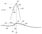
- FIG. 1 shows the lattice defect density D V in the depth direction of hydrogen chemical concentration C H, each distribution of the doping concentration D d and the impurity chemical concentration C I.
- Lattice defect density D V of the comparative example, the hydrogen chemical concentration C H shows each distribution of the doping concentration D d and the impurity chemical concentration C I.
- It is a flowchart which shows an example of the manufacturing method of a semiconductor device 100. It is a flowchart which shows another example of the manufacturing method of a semiconductor device 100. It is a figure explaining the semiconductor device 100 which concerns on the manufacturing method of FIG. In the position shown in line A-A of FIG.
- FIG. 6 shows the lattice defect density D V in the depth direction of hydrogen chemical concentration C H, each distribution of the doping concentration D d and the impurity chemical concentration C I. It is a figure which shows another example of the 1st doping concentration peak 111. It is a figure explaining the relationship between the hydrogen chemical concentration peak 131 and the first doping concentration peak 111. It is a figure explaining the relationship between the impurity chemical concentration peak 141 and the second doping concentration peak 121. It is a figure explaining the inclination of the lower hem 142. It is a figure explaining another definition of the standardization of the inclination of the lower hem 112. It is a figure explaining another definition of the standardization of the inclination of the lower hem 122.
- one side in the direction parallel to the depth direction of the semiconductor substrate is referred to as "upper” and the other side is referred to as “lower”.
- the upper surface is referred to as the upper surface and the other surface is referred to as the lower surface.
- the “up” and “down” directions are not limited to the direction of gravity or the direction when the semiconductor device is mounted.
- Cartesian coordinate axes of the X-axis, the Y-axis, and the Z-axis only specify the relative positions of the components and do not limit the specific direction.
- the Z axis does not limit the height direction with respect to the ground.
- the + Z-axis direction and the ⁇ Z-axis direction are opposite to each other. When the positive and negative directions are not described and the Z-axis direction is described, it means the direction parallel to the + Z-axis and the -Z-axis.
- the X-axis and the Y-axis are orthogonal axes parallel to the upper surface and the lower surface of the semiconductor substrate. Further, the axis perpendicular to the upper surface and the lower surface of the semiconductor substrate is defined as the Z axis.
- the direction of the Z axis may be referred to as a depth direction. Further, in the present specification, the direction parallel to the upper surface and the lower surface of the semiconductor substrate including the X-axis and the Y-axis may be referred to as a horizontal direction.
- the region from the center in the depth direction of the semiconductor substrate to the upper surface of the semiconductor substrate may be referred to as the upper surface side.
- the region from the center of the semiconductor substrate in the depth direction to the lower surface of the semiconductor substrate may be referred to as the lower surface side.
- the center position of the semiconductor substrate in the depth direction may be referred to as Zc.
- error When referred to as “same” or “equal” in the present specification, it may include a case where there is an error due to manufacturing variation or the like.
- the error is, for example, within 10%.
- the conductive type of the doping region doped with impurities is described as P type or N type.
- an impurity may mean, in particular, either an N-type donor or a P-type acceptor, and may be referred to as a dopant.
- doping means that a donor or acceptor is introduced into a semiconductor substrate to obtain a semiconductor exhibiting an N-type conductive type or a semiconductor exhibiting a P-type conductive type.
- the doping concentration means the concentration of a donor or the concentration of an acceptor in a thermal equilibrium state.
- the net doping concentration means the net concentration of the donor concentration as the concentration of positive ions and the acceptor concentration as the concentration of negative ions, including the polarity of the charge.
- the donor concentration N D, the acceptor concentration and N A, the net doping concentration of the net at any position is N D -N A.
- the net doping concentration may be simply referred to as a doping concentration.
- the donor has the function of supplying electrons to the semiconductor.
- the acceptor has a function of receiving electrons from a semiconductor.
- Donors and acceptors are not limited to the impurities themselves.
- a VOH defect in which pores (V), oxygen (O) and hydrogen (H) are bonded in a semiconductor functions as a donor that supplies electrons.
- VOH defects are sometimes referred to herein as hydrogen donors.
- the description of P + type or N + type means that the doping concentration is higher than that of P type or N type
- the description of P-type or N-type means that the doping concentration is higher than that of P type or N type. It means that the concentration is low.
- the unit system of the present specification is the SI unit system. The unit of length may be displayed in cm, but various calculations may be performed after converting to meters (m).
- the chemical concentration refers to the atomic density of impurities measured regardless of the state of electrical activation.
- the chemical concentration (atomic density) can be measured by, for example, secondary ion mass spectrometry (SIMS).
- the net doping concentration described above can be measured by a voltage-capacity measurement method (CV method).
- the carrier concentration measured by the spread resistance measurement method (SR method) may be used as the net doping concentration.
- the carrier concentration measured by the CV method or the SR method may be a value in a thermal equilibrium state.
- the donor concentration is sufficiently higher than the acceptor concentration, so that the carrier concentration in the region may be used as the donor concentration.
- the carrier concentration in the region may be used as the acceptor concentration.
- the doping concentration in the N-type region may be referred to as the donor concentration
- the doping concentration in the P-type region may be referred to as the acceptor concentration.
- the peak value may be used as the concentration of donor, acceptor or net doping in the region.
- the concentration of donor, acceptor or net doping is substantially uniform, the average value of the concentration of donor, acceptor or net doping in the region may be used as the concentration of donor, acceptor or net doping.
- at lesms / cm 3 or / cm 3 may be used to indicate the concentration per unit volume. This unit is used for the donor or acceptor concentration in the semiconductor substrate, or the chemical concentration. The at Budapestms notation may be omitted.
- the carrier concentration measured by the SR method may be lower than the concentration of the donor or acceptor.
- the carrier mobility of the semiconductor substrate may be lower than the value in the crystalline state. The decrease in carrier mobility occurs when carriers are scattered due to disorder of the crystal structure due to lattice defects or the like.
- the concentration of the donor or acceptor calculated from the carrier concentration measured by the CV method or the SR method may be lower than the chemical concentration of the element indicating the donor or acceptor.
- the donor concentration of phosphorus or arsenic as a donor in a silicon semiconductor, or the acceptor concentration of boron (boron) as an acceptor is about 99% of these chemical concentrations.
- the donor concentration of hydrogen as a donor in a silicon semiconductor is about 0.1% to 10% of the chemical concentration of hydrogen.
- Each concentration in the present specification may be a value at room temperature.
- the value at room temperature may be the value at 300 K (Kelvin) (about 26.9 ° C.).
- the peak position of the distribution may be referred to as the position where the particles are injected, the depth at which the particles are injected, or the like.
- FIG. 1 is a cross-sectional view showing an example of the semiconductor device 100.
- the semiconductor device 100 includes a semiconductor substrate 10.
- the semiconductor substrate 10 is a substrate made of a semiconductor material.
- the semiconductor substrate 10 is a silicon substrate.
- At least one of a transistor element such as an insulated gate bipolar transistor (IGBT) and a diode element such as a freewheeling diode (FWD) is formed on the semiconductor substrate 10.
- a transistor element such as an insulated gate bipolar transistor (IGBT) and a diode element such as a freewheeling diode (FWD) is formed on the semiconductor substrate 10.
- IGBT insulated gate bipolar transistor
- FWD freewheeling diode
- N-type bulk donors are distributed throughout.
- the bulk donor is a donor due to the dopant contained in the ingot substantially uniformly during the production of the ingot that is the source of the semiconductor substrate 10.
- the bulk donor in this example is an element other than hydrogen.
- Bulk donor dopants are, but are not limited to, for example phosphorus, antimony, arsenic, selenium or sulfur.
- the bulk donor in this example is phosphorus.
- Bulk donors are also included in the P-type region.
- the semiconductor substrate 10 may be a wafer cut out from a semiconductor ingot, or may be a chip obtained by fragmenting the wafer.
- the semiconductor ingot may be manufactured by any one of the Czochralski method (CZ method), the magnetic field application type Czochralski method (MCZ method), and the float zone method (FZ method).
- the ingot in this example is manufactured by the MCZ method.
- the oxygen concentration contained in the substrate manufactured by the MCZ method is 1 ⁇ 10 17 to 7 ⁇ 10 17 / cm 3 .
- the oxygen concentration contained in the substrate manufactured by the FZ method is 1 ⁇ 10 15 to 5 ⁇ 10 16 / cm 3 .
- the bulk donor concentration may use the chemical concentration of the bulk donor distributed throughout the semiconductor substrate 10, and may be a value between 90% and 100% of the chemical concentration.
- the semiconductor substrate 10 a non-doped substrate containing no dopant such as phosphorus may be used.
- the bulk donor concentration of the non-doping substrate is, for example, 1 ⁇ 10 10 / cm 3 or more and 5 ⁇ 10 12 / cm 3 or less.
- the bulk donor concentration of the non-doping substrate is preferably 1 ⁇ 10 11 / cm 3 or more.
- the bulk donor concentration of the non-doping substrate is preferably 5 ⁇ 10 12 / cm 3 or less.
- the semiconductor substrate 10 has an upper surface 21 and a lower surface 23.
- the upper surface 21 and the lower surface 23 are two main surfaces of the semiconductor substrate 10.
- the orthogonal axes in the plane parallel to the upper surface 21 and the lower surface 23 are the X-axis and the Y-axis
- the axes perpendicular to the upper surface 21 and the lower surface 23 are the Z-axis.
- Charged particles are injected into the semiconductor substrate 10 from the lower surface 23 to the second depth position Z2.
- the charged particles are, for example, hydrogen ions, helium ions, electrons and the like.
- the semiconductor substrate 10 of this example has an impurity chemical concentration peak 141 such as hydrogen or helium at the second depth position Z2.
- the second depth position Z2 may be a position above the upper surface 21. That is, the charged particles may be injected so as to penetrate the semiconductor substrate 10.
- the depth position is a position in the depth direction (Z-axis direction) of the semiconductor substrate 10.
- the distance from the lower surface 23 to each position may be referred to as a depth position of each position.
- the distance of the second depth position Z2 from the lower surface 23 is Z2.
- the second depth position Z2 may be arranged on the upper surface 21 side of the semiconductor substrate 10 (that is, the region between the upper surface 21 and the central position Zc in the depth direction).
- the average distance (also called range) that the charged particles pass through the inside of the semiconductor substrate 10 can be controlled by the acceleration energy that accelerates the charged particles.
- the acceleration energy is set so that the average range of the charged particles is the distance Z2.
- the average range Z2 of the charged particles may be larger than half the thickness of the semiconductor substrate 10 in the depth direction.
- the region through which the injected charged particles have passed may be referred to as a passing region 106.
- the passage region 106 is from the lower surface 23 of the semiconductor substrate 10 to the second depth position Z2.
- charged particles are injected from the entire lower surface 23 of the semiconductor substrate 10.
- charged particles may be injected into only a portion of the lower surface 23. Thereby, the passing region 106 can be locally formed on the XY plane.
- An N-type buffer region 20 is provided on the lower surface 23 side of the semiconductor substrate 10 (that is, the region between the lower surface 23 and the central position Zc in the depth direction).
- a lower surface region 201 is provided between the buffer region 20 and the lower surface 23.
- the lower surface region 201 is an N-type or P-type region having a higher doping concentration than the high-concentration region 150 described later.
- the lower surface region 201 may be a cathode region or a collector region described later.
- the buffer region 20 suppresses the depletion layer spreading from the upper surface 21 side of the semiconductor substrate 10 reaching the lower surface region 201 (punch-through).
- the buffer region 20 has a single first doping concentration peak 111 in which the doping concentration distribution in the depth direction of the semiconductor substrate 10 is single.
- the first doping concentration peak 111 is located at the first depth position Z1. By providing the first doping concentration peak 111, it is possible to prevent the above-mentioned depletion layer from spreading beyond the first doping concentration peak 111 to the lower surface 23 side.
- the buffer region 20 may include a hydrogen donor.
- hydrogen ions such as protons are injected from the lower surface 23 to the first depth position Z1.
- no impurity ions are locally injected between the first depth position Z1 and the second depth position Z2 other than the hydrogen ions and charged particles described above.
- lattice defects such as single-atomic pores (V) and double-atomic pores (VV), which are mainly pores, are present. It is formed. Atoms adjacent to the vacancies have dangling bonds. Lattice defects include interstitial atoms, dislocations, etc., and in a broad sense, donors and acceptors may also be included. Sometimes referred to simply as a lattice defect. Further, the crystallinity of the semiconductor substrate 10 may be strongly disturbed due to the formation of many lattice defects by injecting charged particles into the semiconductor substrate 10. In the present specification, this disorder of crystallinity may be referred to as disorder.
- oxygen is contained in the entire semiconductor substrate 10.
- the oxygen is intentionally or unintentionally introduced during the manufacture of semiconductor ingots.
- H hydrogen
- V pores
- O oxygen
- the hydrogen injected into the first depth position Z1 is diffused, and the formation of VOH defects is promoted.
- the charged particles injected into the second depth position Z2 are hydrogen ions, hydrogen is also diffused from the second depth position Z2, and the formation of VOH defects is further promoted.
- the VOH defect functions as a donor that supplies electrons.
- VOH defects may be referred to simply as hydrogen donors.
- a hydrogen donor is formed in the passage region 106 of the charged particles.
- the doping concentration of hydrogen donors is lower than the chemical concentration of hydrogen.
- the activation rate may be a value of 0.1% to 30%. In this example, the activation rate is 1% to 5%.
- the donor concentration in the passing region 106 of the semiconductor substrate 10 can be made higher than the bulk donor concentration.
- the semiconductor substrate 10 having a predetermined bulk donor concentration must be prepared according to the characteristics of the element to be formed on the semiconductor substrate 10, particularly the rated voltage or the withstand voltage.
- the donor concentration of the semiconductor substrate 10 can be adjusted by controlling the dose amounts of charged particles and hydrogen ions. Therefore, the semiconductor device 100 can be manufactured by using the semiconductor substrate 10 having a bulk donor concentration that does not correspond to the characteristics of the device or the like.
- the dose amounts of charged particles and hydrogen ions can be controlled with relatively high accuracy. Therefore, the concentration of lattice defects generated by injecting charged particles can be controlled with high accuracy, and the concentration of hydrogen bound to lattice defects can also be controlled with high accuracy. Therefore, the donor concentration in the passage region 106 can be controlled with high accuracy.
- the hydrogen injected into the first depth position Z1 diffuses toward the upper surface 21 to a position farther away.
- the length of the passing region 106 in the Z-axis direction can be increased, and the doping concentration can be easily adjusted over a wide region of the semiconductor substrate 10.
- the buffer region 20 is provided with a plurality of doping concentration peaks in order to suppress the spread of the depletion layer while suppressing the electric field concentration.
- the doping concentration peak on the lowermost surface 23 side is set to the maximum concentration in order to prevent the depletion layer from reaching the lower surface region 201.
- the diffusion of hydrogen injected into the maximum concentration peak of the buffer region 20 causes other doping concentration peaks. It is hindered by the lattice defect formed at the position of. Therefore, hydrogen may not diffuse over the entire passage region 106.
- the buffer region 20 has a single first doping concentration peak 111. Therefore, hydrogen diffusion is not suppressed at least in the buffer region 20. Therefore, the hydrogen injected into the first depth position Z1 is likely to diffuse toward the upper surface 21.
- Figure 2 shows in the position shown in line A-A of FIG. 1, the lattice defect density D V in the depth direction of hydrogen chemical concentration C H, each distribution of the doping concentration D d and the impurity chemical concentration C I ..
- the impurities in this example are helium or hydrogen.
- the horizontal axis of FIG. 2 shows the depth position from the lower surface 23, and the vertical axis shows the hydrogen chemical concentration, the donor concentration, and the impurity chemical concentration per unit volume on the logarithmic axis.
- the lattice defect density DV is the distribution before annealing, and the other concentrations show the distribution after injecting hydrogen ions and charged particles (impurities) and annealing.
- the hydrogen chemical concentration and the impurity chemical concentration in FIG. 2 are measured by, for example, the SIMS method.
- the doping concentration in FIG. 2 is an electrically activated doping concentration measured by, for example, the CV method or the SR method.
- Hydrogen chemical concentration C H of the present embodiment includes a hydrogen chemical concentration peak 131 to a first depth position Z1.
- the hydrogen chemical concentration peak 131 shows a maximum value at the first depth position Z1.
- Impurity chemical concentration C I of the present example has an impurity chemical concentration peak 141 to a second depth position Z2.
- the impurity chemical concentration peak 141 shows a maximum value at the second depth position Z2.
- the doping concentration D d has a first doping concentration peak 111 and a second doping concentration peak 121. Further, the doping concentration D d may have a doping concentration peak in the lower surface region 201.
- the lower surface region 201 of this example has a P-type doping concentration peak.
- a P-type dopant such as boron may be injected into the lower surface region 201.
- the lower surface region 201 may have an N-type doping concentration peak. In this case, an N-type dopant such as phosphorus may be injected into the lower surface region 201.
- the first doping concentration peak 111 of this example is a hydrogen donor in which a lattice defect due to hydrogen ion injection into the first depth position Z1 and hydrogen injected into the first depth position Z1 are bonded. This is the concentration peak of (VOH defect). Therefore, the first doping concentration peak 111 shows a maximum value at the first depth position Z1.
- the second doping concentration peak 121 is a concentration peak of a hydrogen donor in which a lattice defect due to injection of charged particles into the second depth position Z2 and hydrogen diffused from the first depth position Z1 are bonded. .. Therefore, the second doping concentration peak 121 shows a maximum value at the second depth position Z2.
- the position where the first doping concentration peak 111 shows the maximum value does not have to exactly coincide with the first depth position Z1. For example, if the position where the first doping concentration peak 111 shows the maximum value is included in the range of the full width at half maximum of the first hydrogen chemical concentration peak 131 with respect to the first depth position Z1, the first It may be assumed that the doping concentration peak 111 of 1 is substantially located at the first depth position Z1. Similarly, if the position where the second doping concentration peak 121 shows the maximum value is included in the range of the full width at half maximum of the impurity chemical concentration peak 141 with respect to the second depth position Z2, the second It may be assumed that the doping concentration peak 121 is substantially located at the second depth position Z2.
- the doping concentration may be the first doping concentration peak 111.
- Each concentration peak has a lower hem in which the concentration decreases from the apex to the lower surface 23 and an upper hem in which the concentration decreases from the apex to the upper surface 21.
- the hydrogen chemical concentration peak 131 has a lower hem 132 and an upper hem 133.
- the impurity chemical concentration peak 141 has a lower hem 142 and an upper hem 143.
- the first doping concentration peak 111 has a lower hem 112 and an upper hem 113.
- the second doping concentration peak 121 has a lower hem 122 and an upper hem 123.
- the concentration may decrease sharply in the upper hem than in the lower hem. Further, since the doping concentration depends on the hydrogen chemical concentration or the impurity chemical concentration, the concentration may decrease sharply in the upper hem than in the lower hem at each doping concentration peak.
- lattice defect concentration D V is the first depth position Z1 having a first defect density peak 211, a second defect density peak 212 to a second depth position Z2. Further, charged particles passed through the passing region 106 (see FIG. 1) from the second depth position Z2 to the lower surface 23, except for the vicinity of the first depth position Z1 and the second depth position Z2. The resulting lattice defects are formed at a nearly uniform density. As shown by the dotted line in the distribution diagram of the lattice defect density D V of FIG.
- the lattice defect concentration D V is within a range that does not exceed the peak 212 may be increased gradually toward the peak 212. Even when such lattice defect concentration D V increases toward the peak 212, lattice defects caused by the charged particles are passed may be a formed in a substantially uniform density.
- the hydrogen injected into the first depth position Z1 diffuses toward the upper surface 21 by the annealing treatment.
- the buffer region 20 has a single first doping concentration peak 111. Therefore, there are no defect density peaks other than the first defect density peak 211 in the buffer region 20. Therefore, hydrogen is likely to diffuse from the first depth position Z1 to the second depth position Z2.
- a VOH defect hydrogen donor
- the high concentration region 150 is a region where the donor concentration is higher than the bulk donor concentration D b.
- the high concentration region 150 is arranged between the buffer region 20 and the upper surface 21 of the semiconductor substrate 10.
- the high concentration region 150 may be a region having a substantially uniform doping concentration in the depth direction.
- the fact that the doping concentration is almost uniform in the depth direction means that, for example, a region in which the difference between the maximum value and the minimum value of the doping concentration is within 50% of the maximum value of the doping concentration is continuous in the depth direction. May point to.
- the difference may be 30% or less of the maximum value of the doping concentration in the region, and may be 10% or less.
- the value of the doping concentration distribution may be within ⁇ 50% of the average concentration of the doping concentration distribution, and may be within ⁇ 30% with respect to the average concentration of the doping concentration distribution in a predetermined range in the depth direction. Well, it may be within ⁇ 10%.
- the predetermined range W in the depth direction may be as follows as an example. That is, the length from the first depth position Z1 to the second depth position Z2 is Z L , and from the center Z 12 c between Z1 and Z2, the first depth position Z1 side and the second The range may be a section having a length of 0.5 Z L between two points separated by 0.25 Z L on the depth position Z 2 side of the above.
- the length of the predetermined range may be a 0.75Z L, may be a 0.3Z L, it may be 0.9Z L.
- the end position on the upper surface 21 side of the buffer region 20 may be a depth position where a substantially uniform doping concentration in the high concentration region 150 begins to monotonically increase toward the first doping concentration peak 111. ..
- the measurement result of the distribution of the doping concentration D d may include a minute peak due to noise or the like during measurement even in the region where the dopant is not injected.
- the peak A in doping concentration D d, the ratio between the minimum and maximum values of the doping concentration D d in the length within 10 ⁇ m may refer to what is 1.1 times or more.
- the ratio may be 1.2 times or more, and may be 1.5 times or more.
- the peak of each chemical concentration may also refer to one having the ratio.
- the high concentration region 150 may be continuously provided from the first doping concentration peak 111 to the impurity chemical concentration peak 141.
- the high concentration region 150 may be continuously provided from the upper end of the buffer region 20 to the second depth position Z2.
- the length of the high concentration region 150 in the depth direction may be 50% or more, 60% or more, 70% or more, 80% or more of the thickness of the semiconductor substrate 10 in the depth direction. It may be.
- the length of the high concentration region 150 in the depth direction may be 70 ⁇ m or more, 80 ⁇ m or more, 90 ⁇ m or more, or 100 ⁇ m or more.
- the range in which the high concentration region 150 is formed can be easily defined by the second depth position Z2.
- the minimum value of the donor concentration in the high concentration region 150 is higher than the bulk donor concentration D b of the semiconductor substrate 10. That is, the donor concentration of the high concentration region 150 (or doping concentration) throughout the high-concentration region 150 is higher than the bulk donor concentration D b.
- the donor concentration in the high concentration region 150 is determined by the sum of the bulk donor concentration and the hydrogen donor concentration (VOH defect concentration).
- the hydrogen donor concentration can be accurately controlled by the dose amount of the charged particles with respect to the second depth position Z2 and the dose amount of hydrogen ions with respect to the first depth position Z1. Therefore, by sufficiently increasing the hydrogen donor concentration as compared with the bulk donor concentration, it is possible to reduce the variation in the donor concentration in the high concentration region 150 even when the bulk donor concentration varies.
- the donor concentration in the high concentration region 150 may be 2 times or more, 5 times or more, or 10 times or more the bulk donor concentration D b.
- Figure 3 shows the lattice defect density D V of the comparative example, the hydrogen chemical concentration C H, each distribution of the doping concentration D d and the impurity chemical concentration C I.
- the semiconductor device of the comparative example has one or more doping concentration peaks 117 on the upper surface 21 side of the first doping concentration peak 111 in the buffer region 20. Each doping concentration peak 117 is formed by injecting hydrogen ions as an example.
- Hydrogen chemical concentration C H of this example the same depth position and each of the doping concentration peaks 117, having a hydrogen chemical concentration peak 137.
- the lattice defect density D V is the same depth position and each of the hydrogen chemical concentration peaks 137 has a defect density peak 213. That is, the buffer region 20 has one or more defect density peaks 213 on the upper surface 21 side of the first depth position Z1.
- the hydrogen chemical concentration peak 131 is 10 times or more higher than the other hydrogen chemical concentration peaks 137. Therefore, most of the hydrogen diffused from the buffer region 20 to the upper surface 21 side is the hydrogen injected into the first depth position Z1. However, the diffusion of hydrogen injected into the first depth position Z1 is hindered by the defect density peak 213. For example, hydrogen binds to lattice defects, or the presence of lattice defects impedes hydrogen transfer.
- the high concentration region 150 is not formed up to the second depth position Z2, and the low concentration region 181 with a low donor concentration remains.
- the donor concentration in the low concentration region 181 may be comparable to the bulk donor concentration D b.
- the carrier concentration in the low concentration region 181 may be lower than the bulk donor concentration D b. Since almost no hydrogen donor is formed in the low concentration region 181, the donor concentration in the low concentration region 181 is greatly affected by the bulk donor concentration. Therefore, the donor concentration in the low concentration region 181 has a relatively large variation.
- the semiconductor device 100 shown in FIG. 2 since the high concentration region 150 can be formed widely, the variation in the doping concentration can be suppressed, and the characteristics of the semiconductor device 100 can be adjusted accurately.
- the high-concentration first doping concentration peak 111 can be arranged in the vicinity of the lower surface 23 to suppress the decrease in the avalanche tolerance, and the high-concentration region 150 can be formed up to the vicinity of the upper surface 21. ..
- the distance between the first depth position Z1 and the lower surface 23 may be 5 ⁇ m or less, and may be 3 ⁇ m or less.
- FIG. 4 is a flowchart showing an example of a manufacturing method of the semiconductor device 100.
- the structure on the upper surface 21 side of the semiconductor substrate 10 is formed.
- the structure on the upper surface 21 side includes at least a part of a gate trench, a dummy trench, an emitter region, a base region, a storage region, an interlayer insulating film, an emitter electrode, and a gate wiring, which will be described later.
- all these structures may be formed.
- the lower surface 23 side of the semiconductor substrate 10 is ground to adjust the thickness of the semiconductor substrate 10.
- the thickness of the semiconductor substrate 10 may be adjusted according to the withstand voltage that the semiconductor device 100 should have.
- the lower surface region 201 is formed in the region in contact with the lower surface 23 of the semiconductor substrate 10.
- the lower surface region 201 may be formed by injecting an N-type dopant or a P-type dopant from the lower surface 23 and locally annealing the vicinity of the lower surface 23 with a laser or the like.
- the first injection step S406 includes a charged particle injection step S408 and a hydrogen injection step S410.
- charged particles are injected from the lower surface 23 of the semiconductor substrate 10 to the second depth position Z2.
- the charged particles may be hydrogen ions, helium ions, or electron beams.
- hydrogen ions are injected from the lower surface 23 of the semiconductor substrate 10 into the first depth position Z1.
- hydrogen ions are injected into the first position Z1 so that the hydrogen chemical concentration distribution has a single peak in the region on the lower surface 23 side of the second depth position Z2.
- a peak of hydrogen chemical concentration may exist at the second depth position Z2. Either the charged particle injection step S408 or the hydrogen injection step S410 may be performed first.
- the semiconductor substrate 10 is annealed.
- the semiconductor substrate 10 is put into an annealing furnace to anneal the entire semiconductor substrate 10.
- a high concentration region 150 is formed between the first depth position Z1 and the second depth position Z2.
- the annealing step S412 is preferably performed under the condition that the hydrogen injected into the first depth position Z1 can be diffused to the second depth position Z2.
- the annealing temperature in the annealing step S412 is 350 ° C. or higher and 400 ° C. or lower.
- the annealing temperature may be 360 ° C. or higher and may be 380 ° C. or lower.
- the annealing time in the annealing step S412 may be 30 minutes or more, 1 hour or more, or 3 hours or more.
- the annealing time may be 10 hours or less, and may be 7 hours or less.
- a metal electrode is formed on the lower surface 23 of the semiconductor substrate 10.
- the metal electrode may be a collector electrode described later. Further, even if an impurity such as helium is injected into the semiconductor substrate 10 between the annealing step S412 and the lower surface side electrode forming step S414, lattice defects are locally formed and the carrier lifetime is adjusted. good.
- FIG. 5 is a flowchart showing another example of the manufacturing method of the semiconductor device 100.
- the manufacturing method of this example differs from the example shown in FIG. 4 in that it further includes a grinding step S500, a second injection step S502, and a second annealing step S504.
- Other steps may be similar to the example shown in FIG.
- the lower surface region forming step S404 is not performed before the first injection step S406.
- the lower surface 23 side of the semiconductor substrate 10 is ground in the grinding step S500.
- the lower surface 23 is ground so as to remove the region including the first depth position Z1 from the semiconductor substrate 10.
- a part of the upper hem 113 of the first doping concentration peak 111 may be ground so as to remain on the semiconductor substrate 10, and the upper hem 113 may be ground so as not to remain on the semiconductor substrate 10. .
- the semiconductor substrate 10 may be ground so that the high concentration region 150 is exposed on the lower surface 23.
- the thickness of the semiconductor substrate 10 ground by the grinding step S402 and the grinding step S500 is a thickness corresponding to a predetermined withstand voltage.
- the grinding amount in the grinding step S402 and the grinding step S500 may be arbitrarily set. Grinding step S402 may be omitted.
- the lower surface region forming step S404 the lower surface region 201 is formed.
- the N-type dopant is injected into the third depth position Z3.
- the third depth position Z3 is a position where the buffer region 20 should be formed.
- the N-type dopant may be hydrogen or may be a dopant other than hydrogen such as phosphorus.
- the semiconductor substrate 10 is annealed.
- the N-type dopant injected into the third depth position Z3 is activated to become a donor.
- the buffer area 20 can be formed.
- the entire semiconductor substrate 10 may be annealed, or may be locally annealed.
- a metal electrode is formed on the lower surface 23 of the semiconductor substrate 10.
- FIG. 6 is a diagram illustrating a semiconductor device 100 according to the manufacturing method of FIG.
- the lower surface of the semiconductor substrate 10 before being ground by the grinding step S500 is the lower surface 23-2, and the lower surface after grinding is the lower surface 23-1.
- first injection step S406 hydrogen ions are injected from the lower surface 23-2 to the first depth position Z1, and charged particles are injected from the lower surface 23-2 to the second depth position Z2. Further, the hydrogen injected into the first depth position Z1 is diffused by the first annealing step S412.
- the lower surface 23-2 is ground to remove the region including the first depth position Z1.
- the lower surface region forming step S404 the lower surface region 201 is formed in the region in contact with the lower surface 23-1.
- the N-type dopant is injected into the third depth position Z3 by the second injection step S502.
- the semiconductor substrate 10 is annealed in the second annealing step S504 to activate the N-type dopant injected into the third depth position Z3 to form the buffer region 20.
- Figure 7 shows in the position shown in line A-A of FIG. 6, the lattice defect density D V in the depth direction of hydrogen chemical concentration C H, each distribution of the doping concentration D d and the impurity chemical concentration C I ..
- the impurities in this example are helium or hydrogen.
- the lattice defect density D V the lattice formed when the hydrogen ion implantation or the like first depth position Z1, the second depth position Z2, the third depth position Z3 It shows the defect density. That is, the lattice defect density D V, the lattice defects formed when forming the lower surface region 201 is omitted.
- the lattice defect density D V the lattice defects formed when forming the lower surface region 201 is omitted.
- the lattice defect concentration D V is within a range that does not exceed the peak 212 may be increased gradually toward the peak 212.
- the mode in which the lattice defect density DV is increasing is shown by a dotted line. Even when such lattice defect concentration D V increases toward the peak 212, lattice defects caused by the charged particles are passed may be a formed in a substantially uniform density. It also shows the density including lattice defects that have become hydrogen donors by annealing. Concentrations other than the lattice defect density indicate the distribution after the second annealing step S504.
- a high concentration of hydrogen is injected into the first depth position Z1 in order to diffuse hydrogen to the second depth position Z2. Therefore, at the first depth position Z1, a hydrogen donor having a concentration higher than that of the hydrogen donor that the buffer region 20 should have may be formed.
- the region including the first depth position Z1 is ground by the grinding step S500.
- the N-type dopant having the concentration that the buffer region 20 should have is injected into the third depth position Z3.
- a defect density peak 214 is formed at the third depth position Z3 by injecting an N-type dopant.
- the defect density peak 214 is formed after the first annealing step S412, it does not interfere with the diffusion of hydrogen injected into the first depth position Z1.
- the hydrogen chemical concentration peak 131 at the first depth position Z1 is removed.
- the hydrogen chemical concentration CH gradually decreases from the lower surface 23 toward the second depth position Z2.
- the first doping concentration peak 111 is a concentration peak of an N-type dopant other than the hydrogen donor.
- hydrogen may be injected into the third depth position Z3.
- the first doping concentration peak 111 is the concentration peak of the hydrogen donor.
- the hydrogen chemical concentration C H has a chemical concentration peak (not shown) to a first depth position Z1.
- FIG. 8 is a diagram showing another example of the first doping concentration peak 111.
- the first doping concentration peak 111 of this example may be applied to each of the examples described in FIGS. 1 to 7.
- the first doping concentration peak 111 of this example is a concentration peak containing both a hydrogen donor and an N-type dopant other than the hydrogen donor.
- the N-type dopant is phosphorus.
- the N-type dopant is selenium or arsenic.
- FIG. 8 shows the phosphate chemical concentration C P with a broken line.
- Phosphorus chemical concentration C P has the chemical concentration peak 119 to a first depth position Z1.
- phosphorus doping concentration D P is the concentration of the donor of activated by a one-dot chain line.
- Doping concentration D P is the concentration multiplied by the activation rate of phosphorus to the phosphorus chemical concentration C P.
- the activation rate of phosphorus may be 1.
- the doping concentration D P it may be used phosphorus chemical concentration C P.
- Doping concentration D1 of the first doping concentration peak 111 is substantially equal to the doping concentration D P corresponding to the phosphorus chemical concentration C P, and the density D H of hydrogen donor, the sum of the bulk donor concentration D b.
- Hydrogen may be injected into the semiconductor substrate 10 at the first depth position Z1.
- the hydrogen chemical concentration C H has a peak in the first depth position Z1.
- the hydrogen chemical concentration C H may not have a peak at a first depth position Z1.
- the first doping concentration peak 111 may include a hydrogen donor formed by diffusing hydrogen injected into the ground region as shown in FIG. 7.
- the injection of an N-type dopant such as phosphorus may be performed after the injection of hydrogen ions.
- FIG. 9A is a diagram illustrating the relationship between the hydrogen chemical concentration peak 131 and the first doping concentration peak 111.
- the slope 134 of the lower hem 132 of the hydrogen chemical concentration peak 131 is used to normalize the slope 114 of the lower hem 112 of the first doping concentration peak 111.
- the standardization is, for example, a process of dividing the slope 114 by the slope 134.
- the inclination of the lower hem may be the inclination between the position where the concentration shows the maximum value and the position where the concentration is a predetermined ratio to the maximum value.
- the predetermined ratio may be 80%, 50%, 10%, 1%, or any other ratio may be used.
- the slope of the concentration distribution between the first depth position Z1 and the lower surface 23 of the semiconductor substrate 10 may be used.
- the slope 134 of the hydrogen chemical concentration peak 131 is given by (H1-aH1) / (Z1-Z4), and the slope 114 of the first doping concentration peak 111 is (D1-aD1) / (. It is given by Z1-Z5).
- H1 is the hydrogen chemical concentration at the first depth position Z1
- D1 is the doping concentration at the first depth position Z1
- a is a predetermined ratio
- Z4 is below the hydrogen chemical concentration peak 131.
- Z5 is the depth at which the hydrogen concentration becomes aH1 at the side hem 132
- Z5 is the depth at which the doping concentration becomes aD1 at the lower hem 112 at the first doping concentration peak 111.
- the slope 114 when the slope 114 is standardized with the slope 134, it becomes (D1-aD1) (Z1-Z4) / ⁇ (H1-aH1) (Z1-Z5) ⁇ .
- ⁇ be the slope obtained by normalizing the slope 114 with the slope 134.
- FIG. 9B is a diagram illustrating the relationship between the impurity chemical concentration peak 141 and the second doping concentration peak 121.
- hydrogen ions are injected as charged particles at the second depth position Z2.
- the slope 144 of the lower hem 142 of the impurity chemical concentration peak 141 is used to normalize the slope 124 of the lower hem 142 of the second doping concentration peak 121.
- the slope 144 of the impurity chemical concentration peak 141 is given by (H2-aH2) / (Z2-Z6), and the slope 124 of the second doping concentration peak 121 is (D2-aD2) / (Z2). -Z7) is given.
- H2 is the hydrogen chemical concentration at the second depth position Z2
- D2 is the doping concentration at the second depth position Z2
- a is a predetermined ratio
- Z6 is below the impurity chemical concentration peak 141.
- Z7 is the depth at which the hydrogen chemical concentration is aH2 at the side hem 142
- Z7 is the depth at which the doping concentration is aD2 at the lower hem 122 at the second doping concentration peak 121.
- the ratio a used to normalize the slope of the second doping concentration peak 121 may be the same as or different from the ratio a used to normalize the slope of the first doping concentration peak 111. ..
- the slope 124 when the slope 124 is standardized with the slope 144, it becomes (D2-aD2) (Z2-Z6) / ⁇ (Z2-Z7) (H2-aH2) ⁇ .
- ⁇ be the slope obtained by normalizing the slope 124 with the slope 144.
- the normalized slope ⁇ of the lower hem 122 of the second doping concentration peak 121 is smaller than the normalized slope ⁇ of the lower hem 112 of the first doping concentration peak 111. That is, the second doping concentration peak 121 has a gentler peak with respect to the peak of the hydrogen chemical concentration than the first doping concentration peak 111. By injecting hydrogen ions so that such a second doping concentration peak 121 is formed, a high concentration region 150 having a flat concentration distribution can be formed. Further, by forming the second doping concentration peak 121 into a gentle shape, it is possible to moderate the change in the doping concentration at the tip of the high concentration region 150.
- the normalized slope ⁇ of the lower hem 122 of the second doping concentration peak 121 may be less than or equal to 1 times the normalized slope ⁇ of the lower hem of the first doping concentration peak 111. It may be 1 times or less, and may be 0.01 times or less.
- the inclination 144 of the lower hem 142 of the impurity chemical concentration peak 141 may be smaller than the inclination 145 of the upper hem 143.
- the chemical concentration distribution of hydrogen injected deep from the lower surface 23 may draw a gentle hem toward the lower surface 23, so by comparing the inclination 144 of the lower hem 142 with the inclination 145 of the upper hem 143. , It may be possible to determine whether or not the hydrogen injected into the second depth position Z2 is injected from the lower surface 23 side.
- the slope 145 is given by (H2-aH2) / (Z8-Z2).
- the slope 125 is given by (D2-aD2) / (Z9-Z2).
- Z8 is the depth at which the hydrogen chemical concentration is aH2 at the upper hem 143 of the impurity chemical concentration peak 141
- Z9 is the depth at which the doping concentration is aD2 at the upper hem 123 of the second doping concentration peak 121.
- the slope 124 of the lower hem 122 of the second doping concentration peak 121 is larger than the slope 125 of the upper hem 123, but the second doping concentration peak 121 is similar to the impurity chemical concentration peak 141.
- the inclination 124 of the lower hem 122 may be smaller than the inclination 125 of the upper hem 123.
- FIG. 9C is a diagram illustrating the inclination of the lower hem 142.
- the inclination of the lower hem 142 may be considered as follows.
- the width (10% total width) between the two positions P10 and P11 having a concentration of 10% (0.1 ⁇ H2) of the peak concentration H2 is set. , FW 10% M.
- the two positions P10 and P11 are the two positions closest to the second depth position Z2 among the points where the hydrogen chemical concentration is 0.1 ⁇ H2 with the second depth position Z2 in between.
- the position on the hydrogen chemical concentration peak 131 side is designated as Z10.
- the slope of the doping concentration at position Z10 is almost flat.
- the slope of the hydrogen chemical concentration at position Z10 is more than 100 times the slope of the doping concentration at position Z10.
- the slope of the hydrogen chemical concentration at position Z10 may be 100 times or more, or 1000 times or more, the slope of the doping concentration at position Z10.
- FIG. 10A is a diagram illustrating another definition of normalization of the inclination of the lower hem 112.
- the position Z4 is a predetermined position here.
- Position Z4 is hydrogen chemical concentration C H and doping concentration D d is as long as it is a position that is the lower side skirt 132,112 at the lower surface 23 side than the first depth position Z1. Let the hydrogen chemical concentration at position Z4 be a ⁇ H1 and the doping concentration be b ⁇ D1.
- a is the ratio of the hydrogen chemical concentration at the position Z4 to the concentration H1 of the hydrogen chemical concentration peak 131 at the first depth position Z1.
- b is the ratio of the doping concentration at position Z3 to the concentration D1 at the first doping concentration peak 111 at the first depth position Z1.
- the slope ratio ⁇ that standardizes the ratio of the slopes of the hydrogen chemical concentration and the doping concentration in the sections Z4 to Z1 and the ratio of the slopes is introduced.
- the ratio of the slopes of the hydrogen chemical concentration in the sections Z4 to Z1 is defined as (H1 / aH1) / (Z1-Z4).
- the ratio of the slopes of the donor concentration in the sections Z4 to Z1 is defined as (D1 / bD1) / (Z1-Z4).
- the slope ratio ⁇ which is the ratio of the slopes of the hydrogen chemical concentration in the sections Z4 to Z1, and the ratio of the slopes of the doping concentration is standardized, is set to ⁇ (D1 / bD1) / (Z1-Z4) ⁇ / ⁇ (H1 / aH1). ) / (Z1-Z4) ⁇ .
- the normalized slope ratio ⁇ becomes a simple ratio a / b by calculating the above equation.
- FIG. 10B is a diagram illustrating another definition of standardization of the inclination of the lower hem 122.
- an index ⁇ similar to the index ⁇ is introduced.
- the position Z6 is a predetermined position here.
- the position Z6 may be a position where the hydrogen chemical concentration and the doping concentration are lower hem 142 and 122 on the lower surface 23 side than the second depth position Z2. Let the hydrogen chemical concentration at position Z6 be c ⁇ H2 and the doping concentration be d ⁇ D2.
- c is the ratio of the hydrogen chemical concentration at the position Z6 to the hydrogen chemical concentration H2 at the second depth position Z2.
- d is the ratio of the doping concentration at position Z6 to the concentration D2 at the second doping concentration peak 121 at the second depth position Z2.
- the slope ratio ⁇ that standardizes the slope ratios of the hydrogen chemical concentration and the doping concentration in the sections Z6 to Z2 and the slope ratio is introduced.
- the ratio of the slopes of the hydrogen chemical concentration in the sections Z6 to Z2 is defined as (H2 / cH2) / (Z2-Z6).
- the ratio of the slopes of the doping concentration in the sections Z6 to Z2 is defined as (D2 / dD2) / (Z2-Z6).
- the slope ratio ⁇ which is the ratio of the slopes of the hydrogen chemical concentration in the sections Z6 to Z2 and the ratio of the slopes of the doping concentration is standardized, is set to ⁇ (D2 / dD2) / (Z2-Z6) ⁇ / ⁇ (H2 / cH2). ) / (Z2-Z6) ⁇ .
- the normalized slope ratio ⁇ becomes a simple ratio (c / d) by calculating the above equation.
- the hydrogen chemical concentration distribution and the doping concentration distribution often have similar figures.
- the similar figure means that the doping concentration distribution reflects the hydrogen chemical concentration distribution, for example, when the horizontal axis is the depth and the vertical axis is the common logarithm of the concentration. That is, in the predetermined sections Z4 to Z1, hydrogen ions are implanted and further annealed, so that the doping concentration distribution reflects the hydrogen chemical concentration distribution.
- H1 of the hydrogen chemical concentration peak 131 is 1 ⁇ 10 17 at réellems / cm 3 and the hydrogen chemical concentration aH1 at position Z4 is 2 ⁇ 10 16 at réellems / cm 3
- a is 0.2.
- the normalized slope ratio ⁇ is 1 because it is a / b. That is, at the first depth position Z1 near the lower surface 23, the ratio a of the slope of the hydrogen chemical concentration distribution and the ratio b of the slope of the doping concentration distribution are almost the same value, and it can be said that they are similar figures.
- the hydrogen chemical concentration distribution and the doping concentration distribution do not have to be similar figures. That is, in the predetermined sections Z6 to Z2, the doping concentration distribution does not have to reflect the hydrogen chemical concentration distribution.
- the hydrogen chemical concentration H2 of the impurity chemical concentration peak 141 is 1 ⁇ 10 16 at réellems / cm 3
- the hydrogen chemical concentration cH2 at position Z6 is 1 ⁇ 10 15 at réellems / cm 3
- c is 0.1. ..
- the normalized slope ratio ⁇ is 0.2 because it is c / d. That is, at the second depth position Z2 sufficiently deep from the lower surface 23, the ratio c of the slope of the hydrogen chemical concentration distribution is 0.2 times smaller than the ratio d of the slope of the doping concentration distribution, which is far from the similarity. It can be said to show the shape.
- the standardized slope ratio ⁇ may be larger than the standardized slope ratio ⁇ .
- the slope ratio ⁇ may be 1.1 or more, 1.5 or more, and 2 or more. Alternatively, it may be 10 or more, and may be 100 or more.
- the actual positions of the hydrogen chemical concentration peak 131 and the impurity chemical concentration peak 141 may differ from the actual positions of the first doping concentration peak 111 and the second doping concentration peak 121.
- the position of the chemical concentration peak and the position of the doping concentration do not match in this way, the position of the chemical concentration peak is set to the first depth position Z1 or the second depth position Z2, and the doping concentration is the first depth.
- the concentration at the vertical position Z1 or the second depth position Z2 may be used as the peak position for convenience. This makes it possible to calculate according to the above definition.
- 11 to 19 are diagrams illustrating an example of a method of determining the bulk donor concentration and the preferred range of donor concentration in the high concentration region 150.
- the bulk donor concentration and the donor concentration are set so that the final donor concentration (doping concentration) in the high concentration region 150 becomes a relatively stable concentration even when the bulk donor concentration varies. ..
- the bulk donor concentration specification value is a specification value specified by the semiconductor wafer manufacturer. If the specification value has a range, the median value of the specification value may be used.
- the concentration of hydrogen donor (VOH defect) be NH .
- the variation in hydrogen donor concentration NH is negligibly small compared to the variation in bulk donor concentration.
- the variation of the hydrogen donor concentration NH is set to 0.
- the target value of the final donor concentration be NF0 .
- the final donor concentration actually obtained is defined as N Fre .
- the above-mentioned concentrations are all concentrations per unit volume (/ cm 3 ).
- Target value N F0 final donor concentration the specification value N B0 bulk donor concentration, since the result of the addition of hydrogen donor concentration N H, is given by the following equation.
- N F0 N H + N B0 ... Equation (1)
- the actual donor concentration N Fre is obtained by adding the hydrogen donor concentration NH to the actual bulk donor concentration N Bre , and is therefore given by the following equation.
- N Fre N H + N Bre ... Equation (2)
- the parameter ⁇ is the ratio of the actual bulk donor concentration N Bre and the specification value N B0, and indicates that the actual bulk donor concentration N Bre deviates from the specification value N B0 as the distance from 1 increases.
- the parameter ⁇ is the ratio of the actual donor concentration N Fre and the target value N F0, and indicates that the actual donor concentration N Fre deviates from the target value N F 0 as the distance from 1 increases. That is, if ⁇ is sufficiently close to 1, even if the actual bulk donor concentration N Bre deviates by ⁇ times from the specification value N B 0 , the actual donor concentration N Fre becomes the target value almost independently of ⁇ . It shows that it is almost the same as NF0.
- the specific resistance variation of the silicon wafer manufactured by the FZ method in which the variation of the bulk donor concentration is relatively small is generally as follows.
- the actual donor concentration N Fre is affected by the variability ( ⁇ ) of the actual bulk donor concentration N Bre.
- the variation in the hydrogen donor concentration NH can be regarded as almost 0 as compared with the variation in the bulk donor concentration N Bre. Therefore, by reducing the specifications N B0 Bulk donor concentration to the target value N F0 donor concentration, it is possible to reduce the proportion of the component which varies in the donor concentration N Fre.
- Parameter epsilon ' is the target value N F0 donor concentration
- the specification value N B0 Bulk donor concentration epsilon' is set to be smaller by a parameter meaning. If ⁇ 'is set to a value smaller than 1 in the range where it does not become 0, it is examined whether ⁇ approaches 1 sufficiently without depending on ⁇ .
- N B0 N F0 / ⁇ ⁇ ⁇ Equation (7)
- N Fre (1-1 / ⁇ ) N F0 + ⁇ N B0 ... Equation (9)
- Eq. (7) into Eq. (9), the following equation is obtained.
- ⁇ 1 + ⁇ '( ⁇ -1) ⁇ ⁇ ⁇ Equation (12)
- FIG. 11 is a graph showing the relationship between ⁇ 'and ⁇ represented by the equation (12) for each ⁇ .
- ⁇ indicates the ratio of the actual donor concentration N Fre to the target value N F0
- ⁇ indicates the ratio of the actual bulk donor concentration N Bre to the specified value N B 0 .
- the permissible value of ⁇ is 0.85 or more and 1.15 or less.
- the specification value N B0 bulk donor concentration 0.5 times the target value N F0 donor concentration or less, that, the epsilon 'and 0.5 or less.
- ⁇ is 1.15 or less, which is within the permissible range.
- the actual donor concentration N Fre is 1.15 times or less of the target value N F0.
- ⁇ is 0.7, if ⁇ 'is 0.5 or less, ⁇ is within the permissible range.
- ⁇ 'approaches 0, ⁇ converges to 1. For example, in the case of ⁇ 2, if ⁇ 'is approximately 0.2 or less, ⁇ is within the permissible range.
- ranges A to D can be considered as a preferable range of ⁇ '.
- ⁇ 'is 0.5 and ⁇ is within the range of 0.7 to 1.3, ⁇ is within the permissible range.
- the specification value N B0 of the bulk donor concentration is 1 ⁇ 10 14 / cm 3 and ⁇ 'is 0.001
- the target value N F0 of the donor concentration is 1 ⁇ 10 11 / cm 3 and is about 46000 ⁇ cm.
- the specification value N B0 of the bulk donor concentration is 1 ⁇ 10 14 / cm 3 and ⁇ 'is 0.001
- the target value N F0 of the donor concentration is 1 ⁇ 10 11 / cm 3 and is about 46000 ⁇ cm.
- ⁇ ' is preferably 0.1 or less, and more preferably 0.02 or less.
- ranges E to H can be considered.
- ⁇ 'is 0.1 and ⁇ is in the range of approximately 0.05 (not shown) to 3.0, ⁇ is sufficiently within the permissible range.
- N B0 Bulk donor concentration is that 1 ⁇ 10 14 / cm 3, if epsilon 'is 0.1, the target value N F0 donor concentration is 1 ⁇ 10 13 / cm 3, about 460 ⁇ cm Corresponds to.
- the actual donor concentration N Fre corresponds to the donor concentration in the high concentration region 150.
- the withstand voltage of the semiconductor device 100 is almost determined by the donor concentration in the high concentration region 150, which occupies a large region in the semiconductor substrate 10. Therefore, the rated voltage of the semiconductor device 100 determines a preferable range of the donor concentration N Fre in the high concentration region 150.
- range of bulk donor concentration N Bre to the donor concentration N Fre can be stabilized is determined.
- FIG. 12 is a diagram showing an example of a preferable range of the bulk donor concentration N Bre.
- the donor concentration N Fre (/ cm 3 ) at the center Zc in the depth direction of the semiconductor substrate 10 is (9.2245 ⁇ 10 15 ) / x or more and (9.2245 ⁇ 10 16 ) / x. be.
- x is the rated voltage (V).
- the donor concentration N Fre (/ cm 3 ) was determined by referring to the doping concentration in the drift region of a general semiconductor substrate formed by the FZ method, but the doping concentration in the drift region of the semiconductor substrate formed by the MCZ method was determined. You may decide by referring to.
- the upper limit 311 and the lower limit 312 of the preferable range of the donor concentration N Fre (/ cm 3) are shown by broken lines.
- the upper limit 313 and the lower limit 314 of the preferable range of the bulk donor concentration N Bre in the above-mentioned range A ( ⁇ 'is 0.001 or more and 0.5 or less) are shown by solid lines.
- the upper limit 313 of the bulk donor concentration N Bre is a value obtained by multiplying the upper limit 311 of the donor concentration N Fre (/ cm 3 ) by the upper limit value (0.5) of ⁇ '.
- the lower limit 314 of the bulk donor concentration N Bre is a value obtained by multiplying the lower limit 312 of the donor concentration N Fre (/ cm 3 ) by the lower limit value (0.001) of ⁇ '.
- the upper limit 313 and lower limit 314 of the bulk donor concentration N Bre are as follows.
- the unit of the upper limit 313 and the lower limit 314 in each example is (/ cm 3 ).
- x is the rated voltage (V).
- FIG. 13 is a diagram showing an example of a preferable range of the bulk donor concentration N Bre when ⁇ 'is in the range B (0.01 or more and 0.333 or less).
- the upper limit 311 and lower limit 312 of the donor concentration N Fre (/ cm 3) are the same as those in FIG.
- the upper limit 313 of the bulk donor concentration N Bre is a value obtained by multiplying the upper limit 311 of the donor concentration N Fre (/ cm 3 ) by the upper limit value (0.333) of ⁇ '.
- the lower limit 314 of the bulk donor concentration N Bre is a value obtained by multiplying the lower limit 312 of the donor concentration N Fre (/ cm 3 ) by the lower limit value (0.01) of ⁇ '.
- the upper limit 313 and lower limit 314 of the bulk donor concentration N Bre are as follows.
- FIG. 14 is a diagram showing an example of a preferable range of the bulk donor concentration N Bre when ⁇ 'is in the range C (0.03 or more and 0.25 or less).
- the upper limit 311 and lower limit 312 of the donor concentration N Fre (/ cm 3) are the same as those in FIG.
- the upper limit 313 of the bulk donor concentration N Bre is a value obtained by multiplying the upper limit 311 of the donor concentration N Fre (/ cm 3 ) by the upper limit value (0.25) of ⁇ '.
- the lower limit 314 of the bulk donor concentration N Bre is a value obtained by multiplying the lower limit 312 of the donor concentration N Fre (/ cm 3 ) by the lower limit value (0.03) of ⁇ '.
- the upper limit 313 and lower limit 314 of the bulk donor concentration N Bre are as follows.
- FIG. 15 is a diagram showing an example of a preferable range of the bulk donor concentration N Bre when ⁇ 'is in the range D (0.1 or more and 0.2 or less).
- the upper limit 311 and lower limit 312 of the donor concentration N Fre (/ cm 3) are the same as those in FIG.
- the upper limit 313 of the bulk donor concentration N Bre is a value obtained by multiplying the upper limit 311 of the donor concentration N Fre (/ cm 3 ) by the upper limit value (0.2) of ⁇ '.
- the lower limit 314 of the bulk donor concentration N Bre is a value obtained by multiplying the lower limit 312 of the donor concentration N Fre (/ cm 3 ) by the lower limit value (0.1) of ⁇ '.
- the upper limit 313 and lower limit 314 of the bulk donor concentration N Bre are as follows.
- FIG. 16 is a diagram showing an example of a preferable range of the bulk donor concentration N Bre when ⁇ 'is in the range E (0.001 or more and 0.1 or less).
- the upper limit 311 and lower limit 312 of the donor concentration N Fre (/ cm 3) are the same as those in FIG.
- the upper limit 313 of the bulk donor concentration N Bre is a value obtained by multiplying the upper limit 311 of the donor concentration N Fre (/ cm 3 ) by the upper limit value (0.1) of ⁇ '.
- the lower limit 314 of the bulk donor concentration N Bre is a value obtained by multiplying the lower limit 312 of the donor concentration N Fre (/ cm 3 ) by the lower limit value (0.001) of ⁇ '.
- the upper limit 313 and lower limit 314 of the bulk donor concentration N Bre are as follows.
- FIG. 17 is a diagram showing an example of a preferable range of the bulk donor concentration N Bre when ⁇ 'is in the range F (0.002 or more and 0.05 or less).
- the upper limit 311 and lower limit 312 of the donor concentration N Fre (/ cm 3) are the same as those in FIG.
- the upper limit 313 of the bulk donor concentration N Bre is a value obtained by multiplying the upper limit 311 of the donor concentration N Fre (/ cm 3 ) by the upper limit value (0.05) of ⁇ '.
- the lower limit 314 of the bulk donor concentration N Bre is a value obtained by multiplying the lower limit 312 of the donor concentration N Fre (/ cm 3 ) by the lower limit value (0.002) of ⁇ '.
- the upper limit 313 and lower limit 314 of the bulk donor concentration N Bre are as follows.
- -Lower limit 314 (1.84049 x 10 13 ) / x ⁇
- Upper limit 313 (4.60123 ⁇ 10 15 ) / x
- FIG. 18 is a diagram showing an example of a preferable range of the bulk donor concentration N Bre when ⁇ 'is in the range G (0.005 or more and 0.02 or less).
- the upper limit 311 and lower limit 312 of the donor concentration N Fre (/ cm 3) are the same as those in FIG.
- the upper limit 313 of the bulk donor concentration N Bre is a value obtained by multiplying the upper limit 311 of the donor concentration N Fre (/ cm 3 ) by the upper limit value (0.02) of ⁇ '.
- the lower limit 314 of the bulk donor concentration N Bre is a value obtained by multiplying the lower limit 312 of the donor concentration N Fre (/ cm 3 ) by the lower limit value (0.005) of ⁇ '.
- the upper limit 313 and lower limit 314 of the bulk donor concentration N Bre are as follows.
- FIG. 19 is a diagram showing an example of a preferable range of the bulk donor concentration N Bre when ⁇ 'is the range H (0.01 ⁇ 0.002).
- the upper limit 311 and lower limit 312 of the donor concentration N Fre (/ cm 3) are the same as those in FIG.
- the upper limit 313 of the bulk donor concentration N Bre is a value obtained by multiplying the upper limit 311 of the donor concentration N Fre (/ cm 3 ) by the upper limit value (0.01) of ⁇ '.
- the lower limit 314 of the bulk donor concentration N Bre is a value obtained by multiplying the lower limit 312 of the donor concentration N Fre (/ cm 3 ) by the lower limit value (0.01) of ⁇ '.
- the upper limit 313 and lower limit 314 of the bulk donor concentration N Bre are as follows.
- -Lower limit 314 (9.2245 x 10 13 ) / x -Upper limit 313: (9.2245 x 10 14 ) / x
- the upper limit 313 and the lower limit 314 in each range may have a width of ⁇ 20%.
- the curve of the lower limit 314 may be smaller than the intrinsic carrier concentration.
- the intrinsic carrier concentration is 1.45 ⁇ 10 10 / cm 3 at room temperature (for example, 300 K). If the value of the curve of the lower limit 314 is smaller than the intrinsic carrier concentration, the lower limit 314 may be replaced with the intrinsic carrier concentration.
- FIG. 20 is an example of a top view of the semiconductor device 100.
- the positions where each member is projected onto the upper surface of the semiconductor substrate 10 are shown.
- FIG. 20 only a part of the members of the semiconductor device 100 is shown, and some members are omitted.
- the semiconductor device 100 includes the semiconductor substrate 10 described with reference to FIGS. 1 to 19.
- the semiconductor substrate 10 has an end side 102 when viewed from above. When simply referred to as a top view in the present specification, it means that the semiconductor substrate 10 is viewed from the top surface side.
- the semiconductor substrate 10 of this example has two sets of end sides 102 facing each other in a top view. In FIG. 20, the X-axis and the Y-axis are parallel to either end 102. The Z-axis is perpendicular to the upper surface of the semiconductor substrate 10.
- the semiconductor substrate 10 is provided with an active portion 160.
- the active portion 160 is a region in which a main current flows in the depth direction between the upper surface and the lower surface of the semiconductor substrate 10 when the semiconductor device 100 operates.
- An emitter electrode is provided above the active portion 160, but is omitted in FIG. 20.
- the active unit 160 is provided with at least one of a transistor unit 70 including a transistor element such as an IGBT and a diode unit 80 including a diode element such as a freewheeling diode (FWD).
- a transistor unit 70 including a transistor element such as an IGBT and a diode unit 80 including a diode element such as a freewheeling diode (FWD).
- the transistor portion 70 and the diode portion 80 are alternately arranged along a predetermined arrangement direction (X-axis direction in this example) on the upper surface of the semiconductor substrate 10.
- the active portion 160 may be provided with only one of the transistor portion 70 and the diode portion 80.
- the symbol “I” is attached to the region where the transistor portion 70 is arranged, and the symbol “F” is attached to the region where the diode portion 80 is arranged.
- the direction perpendicular to the arrangement direction in the top view may be referred to as a stretching direction (Y-axis direction in FIG. 20).
- the transistor portion 70 and the diode portion 80 may each have a longitudinal length in the stretching direction. That is, the length of the transistor portion 70 in the Y-axis direction is larger than the width in the X-axis direction. Similarly, the length of the diode portion 80 in the Y-axis direction is larger than the width in the X-axis direction.
- the stretching direction of the transistor portion 70 and the diode portion 80 may be the same as the longitudinal direction of each trench portion described later.
- the diode portion 80 has an N + type cathode region in a region in contact with the lower surface of the semiconductor substrate 10.
- the region provided with the cathode region is referred to as a diode portion 80. That is, the diode portion 80 is a region that overlaps with the cathode region in the top view.
- a P + type collector region may be provided on the lower surface of the semiconductor substrate 10 in a region other than the cathode region.
- the diode portion 80 may also include an extension region 81 in which the diode portion 80 is extended in the Y-axis direction to the gate wiring described later.
- a collector area is provided on the lower surface of the extension area 81.
- the transistor portion 70 has a P + type collector region in a region in contact with the lower surface of the semiconductor substrate 10. Further, in the transistor portion 70, a gate structure having an N-type emitter region, a P-type base region, a gate conductive portion and a gate insulating film is periodically arranged on the upper surface side of the semiconductor substrate 10.
- the semiconductor device 100 may have one or more pads above the semiconductor substrate 10.
- the semiconductor device 100 of this example has a gate pad 164.
- the semiconductor device 100 may have pads such as an anode pad, a cathode pad, and a current detection pad.
- Each pad is arranged in the vicinity of the end side 102.
- the vicinity of the end side 102 refers to a region between the end side 102 and the emitter electrode in top view.
- each pad may be connected to an external circuit via wiring such as a wire.
- a gate potential is applied to the gate pad 164.
- the gate pad 164 is electrically connected to the conductive portion of the gate trench portion of the active portion 160.
- the semiconductor device 100 includes a gate wiring that connects the gate pad 164 and the gate trench portion. In FIG. 20, the gate wiring is hatched with diagonal lines.
- the gate wiring of this example has an outer peripheral gate wiring 130 and an active side gate wiring 129.
- the outer peripheral gate wiring 130 is arranged between the active portion 160 and the end side 102 of the semiconductor substrate 10 in a top view.
- the outer peripheral gate wiring 130 of this example surrounds the active portion 160 in a top view.
- the region surrounded by the outer peripheral gate wiring 130 in the top view may be the active portion 160.
- the outer peripheral gate wiring 130 is connected to the gate pad 164.
- the outer peripheral gate wiring 130 is arranged above the semiconductor substrate 10.
- the outer peripheral gate wiring 130 may be a metal wiring containing aluminum or the like.
- the active side gate wiring 129 is provided in the active portion 160. By providing the active side gate wiring 129 in the active portion 160, it is possible to reduce the variation in the wiring length from the gate pad 164 in each region of the semiconductor substrate 10.
- the active side gate wiring 129 is connected to the gate trench portion of the active portion 160.
- the active side gate wiring 129 is arranged above the semiconductor substrate 10.
- the active side gate wiring 129 may be wiring formed of a semiconductor such as polysilicon doped with impurities.
- the active side gate wiring 129 may be connected to the outer peripheral gate wiring 130.
- the active side gate wiring 129 of this example is provided so as to extend in the X-axis direction from one outer peripheral gate wiring 130 to the other outer peripheral gate wiring 130 at substantially the center in the Y-axis direction so as to cross the active portion 160. There is.
- the transistor portion 70 and the diode portion 80 may be alternately arranged in the X-axis direction in each divided region.
- the semiconductor device 100 includes a temperature sense unit (not shown) which is a PN junction diode made of polysilicon or the like, and a current detection unit (not shown) which simulates the operation of a transistor unit provided in the active unit 160. May be good.
- a temperature sense unit (not shown) which is a PN junction diode made of polysilicon or the like
- a current detection unit (not shown) which simulates the operation of a transistor unit provided in the active unit 160. May be good.
- the semiconductor device 100 of this example includes an edge termination structure portion 90 between the active portion 160 and the end side 102.
- the edge termination structure 90 of this example is arranged between the outer peripheral gate wiring 130 and the end side 102.
- the edge termination structure 90 relaxes the electric field concentration on the upper surface side of the semiconductor substrate 10.
- the edge termination structure 90 has a plurality of guard rings 92.
- the guard ring 92 is a P-shaped region in contact with the upper surface of the semiconductor substrate 10.
- the guard ring 92 may surround the active portion 160 in top view.
- the plurality of guard rings 92 are arranged at predetermined intervals between the outer peripheral gate wiring 130 and the end side 102.
- the guard ring 92 arranged on the outside may surround the guard ring 92 arranged on the inside.
- the outside refers to the side close to the end side 102, and the inside refers to the side close to the outer peripheral gate wiring 130.
- the edge termination structure 90 may further include at least one of a field plate and a resurf provided in an annular shape surrounding the active portion 160.
- FIG. 21 is an enlarged view of region A in FIG. 20.
- the region A is a region including the transistor portion 70, the diode portion 80, and the active side gate wiring 129.
- the semiconductor device 100 of this example includes a gate trench portion 40, a dummy trench portion 30, a well region 11, an emitter region 12, a base region 14, and a contact region 15 provided inside the upper surface side of the semiconductor substrate 10.
- the gate trench portion 40 and the dummy trench portion 30 are examples of trench portions, respectively.
- the semiconductor device 100 of this example includes an emitter electrode 52 and an active side gate wiring 129 provided above the upper surface of the semiconductor substrate 10.
- the emitter electrode 52 and the active side gate wiring 129 are provided separately from each other.
- An interlayer insulating film is provided between the emitter electrode 52 and the active side gate wiring 129 and the upper surface of the semiconductor substrate 10, but this is omitted in FIG.
- a contact hole 54 is provided so as to penetrate the interlayer insulating film.
- each contact hole 54 is hatched with diagonal lines.
- the emitter electrode 52 is provided above the gate trench portion 40, the dummy trench portion 30, the well region 11, the emitter region 12, the base region 14, and the contact region 15.
- the emitter electrode 52 passes through the contact hole 54 and comes into contact with the emitter region 12, the contact region 15, and the base region 14 on the upper surface of the semiconductor substrate 10. Further, the emitter electrode 52 is connected to the dummy conductive portion in the dummy trench portion 30 through a contact hole provided in the interlayer insulating film.
- the emitter electrode 52 may be connected to the dummy conductive portion of the dummy trench portion 30 at the tip of the dummy trench portion 30 in the Y-axis direction.
- the active side gate wiring 129 is connected to the gate trench portion 40 through a contact hole provided in the interlayer insulating film.
- the active side gate wiring 129 may be connected to the gate conductive portion of the gate trench portion 40 at the tip portion 41 of the gate trench portion 40 in the Y-axis direction.
- the active side gate wiring 129 is not connected to the dummy conductive portion in the dummy trench portion 30.
- the emitter electrode 52 is made of a material containing metal. In FIG. 21, the range in which the emitter electrode 52 is provided is shown. For example, at least a part of the emitter electrode 52 is formed of an aluminum or aluminum-silicon alloy, for example, a metal alloy such as AlSi or AlSiCu.
- the emitter electrode 52 may have a barrier metal formed of titanium, a titanium compound, or the like in the lower layer of the region formed of aluminum or the like. Further, the contact hole may have a plug formed by embedding tungsten or the like so as to be in contact with the barrier metal and aluminum or the like.
- the well region 11 is provided so as to overlap the active side gate wiring 129.
- the well region 11 is extended to a predetermined width so as not to overlap with the active side gate wiring 129.
- the well region 11 of this example is provided away from the end of the contact hole 54 in the Y-axis direction on the active side gate wiring 129 side.
- the well region 11 is a second conductive type region having a higher doping concentration than the base region 14.
- the base region 14 of this example is P-type, and the well region 11 is P + type.
- Each of the transistor portion 70 and the diode portion 80 has a plurality of trench portions arranged in the arrangement direction.
- the transistor portion 70 of this example one or more gate trench portions 40 and one or more dummy trench portions 30 are alternately provided along the arrangement direction.
- the diode portion 80 of this example is provided with a plurality of dummy trench portions 30 along the arrangement direction.
- the diode portion 80 of this example is not provided with the gate trench portion 40.
- the gate trench portion 40 of this example connects two straight portions 39 (portions that are linear along the stretching direction) and two straight portions 39 that extend along the stretching direction perpendicular to the arrangement direction. It may have a tip 41.
- the stretching direction in FIG. 21 is the Y-axis direction.
- the tip portion 41 is provided in a curved shape in a top view.
- the dummy trench portion 30 is provided between the straight portions 39 of the gate trench portion 40.
- One dummy trench portion 30 may be provided between the straight portions 39, and a plurality of dummy trench portions 30 may be provided.
- the dummy trench portion 30 may have a linear shape extending in the stretching direction, and may have a straight portion 29 and a tip portion 31 as in the gate trench portion 40.
- the semiconductor device 100 shown in FIG. 21 includes both a linear dummy trench portion 30 having no tip portion 31 and a dummy trench portion 30 having a tip portion 31.
- the diffusion depth of the well region 11 may be deeper than the depth of the gate trench portion 40 and the dummy trench portion 30.
- the ends of the gate trench portion 40 and the dummy trench portion 30 in the Y-axis direction are provided in the well region 11 in the top view. That is, at the end of each trench in the Y-axis direction, the bottom of each trench in the depth direction is covered with the well region 11. Thereby, the electric field concentration at the bottom of each trench can be relaxed.
- a mesa part is provided between each trench part in the arrangement direction.
- the mesa portion refers to a region sandwiched between trench portions inside the semiconductor substrate 10.
- the upper end of the mesa portion is the upper surface of the semiconductor substrate 10.
- the depth position of the lower end of the mesa portion is the same as the depth position of the lower end of the trench portion.
- the mesa portion of this example is provided on the upper surface of the semiconductor substrate 10 by extending in the stretching direction (Y-axis direction) along the trench.
- the transistor portion 70 is provided with a mesa portion 60
- the diode portion 80 is provided with a mesa portion 61.
- a mesa portion when simply referred to as a mesa portion in the present specification, it refers to each of the mesa portion 60 and the mesa portion 61.
- a base region 14 is provided in each mesa section. Of the base region 14 exposed on the upper surface of the semiconductor substrate 10 in the mesa portion, the region closest to the active side gate wiring 129 is referred to as the base region 14-e. In FIG. 21, the base region 14-e arranged at one end in the extending direction of each mesa portion is shown, but the base region 14-e is also arranged at the other end of each mesa portion. Has been done.
- Each mesa portion may be provided with at least one of a first conductive type emitter region 12 and a second conductive type contact region 15 in a region sandwiched between base regions 14-e in a top view.
- the emitter region 12 of this example is N + type
- the contact region 15 is P + type.
- the emitter region 12 and the contact region 15 may be provided between the base region 14 and the upper surface of the semiconductor substrate 10 in the depth direction.
- the mesa portion 60 of the transistor portion 70 has an emitter region 12 exposed on the upper surface of the semiconductor substrate 10.
- the emitter region 12 is provided in contact with the gate trench portion 40.
- the mesa portion 60 in contact with the gate trench portion 40 may be provided with an exposed contact region 15 on the upper surface of the semiconductor substrate 10.
- Each of the contact region 15 and the emitter region 12 in the mesa portion 60 is provided from one trench portion in the X-axis direction to the other trench portion.
- the contact region 15 and the emitter region 12 of the mesa portion 60 are alternately arranged along the extending direction (Y-axis direction) of the trench portion.
- the contact region 15 and the emitter region 12 of the mesa portion 60 may be provided in a stripe shape along the extending direction (Y-axis direction) of the trench portion.
- an emitter region 12 is provided in a region in contact with the trench portion, and a contact region 15 is provided in a region sandwiched between the emitter regions 12.
- the emitter region 12 is not provided in the mesa portion 61 of the diode portion 80.
- a base region 14 and a contact region 15 may be provided on the upper surface of the mesa portion 61.
- a contact region 15 may be provided in contact with the respective base regions 14-e in the region sandwiched between the base regions 14-e on the upper surface of the mesa portion 61.
- a base region 14 may be provided in a region sandwiched between the contact regions 15 on the upper surface of the mesa portion 61.
- the base region 14 may be arranged over the entire region sandwiched between the contact regions 15.
- a contact hole 54 is provided above each mesa portion.
- the contact hole 54 is arranged in a region sandwiched between the base regions 14-e.
- the contact hole 54 of this example is provided above each region of the contact region 15, the base region 14, and the emitter region 12.
- the contact hole 54 is not provided in the region corresponding to the base region 14-e and the well region 11.
- the contact hole 54 may be arranged at the center of the mesa portion 60 in the arrangement direction (X-axis direction).
- an N + type cathode region 82 is provided in a region adjacent to the lower surface of the semiconductor substrate 10.
- a P + type collector region 22 may be provided on the lower surface of the semiconductor substrate 10 in a region where the cathode region 82 is not provided.
- the boundary between the cathode region 82 and the collector region 22 is shown by a dotted line.
- the cathode region 82 is arranged away from the well region 11 in the Y-axis direction.
- the pressure resistance can be improved by securing the distance between the P-shaped region (well region 11) formed to a deep position and having a relatively high doping concentration and the cathode region 82.
- the end of the cathode region 82 of this example in the Y-axis direction is located farther from the well region 11 than the end of the contact hole 54 in the Y-axis direction.
- the end of the cathode region 82 in the Y-axis direction may be located between the well region 11 and the contact hole 54.
- FIG. 22A is a diagram showing an example of a bb cross section in FIG. 21.
- the bb cross section is an XZ plane passing through the emitter region 12 and the cathode region 82.
- the semiconductor device 100 of this example has a semiconductor substrate 10, an interlayer insulating film 38, an emitter electrode 52, and a collector electrode 24 in the cross section.
- the interlayer insulating film 38 is provided on the upper surface of the semiconductor substrate 10.
- the interlayer insulating film 38 is a film containing at least one layer of an insulating film such as silicate glass to which impurities such as boron and phosphorus are added, a thermal oxide film, and other insulating films.
- the interlayer insulating film 38 is provided with the contact hole 54 described in FIG. 21.
- the emitter electrode 52 is provided above the interlayer insulating film 38.
- the emitter electrode 52 is in contact with the upper surface 21 of the semiconductor substrate 10 through the contact hole 54 of the interlayer insulating film 38.
- the collector electrode 24 is provided on the lower surface 23 of the semiconductor substrate 10.
- the emitter electrode 52 and the collector electrode 24 are made of a metal material such as aluminum.
- the direction (Z-axis direction) connecting the emitter electrode 52 and the collector electrode 24 is referred to as a depth direction.
- the semiconductor substrate 10 has an N-type drift region 19.
- the drift region 19 of this example is an N-shaped region from the lower end of the storage region 16 to the upper end of the buffer region 20.
- the drift region 19 of this example has the high concentration region 150 described in FIGS. 1 to 19. In FIG. 22A, the high concentration region 150 is hatched with diagonal lines.
- the high concentration region 150 may be provided in the transistor section 70, may be provided in the diode section 80, or may be provided in both the transistor section 70 and the diode section 80.
- the high concentration region 150 is a region provided from the upper end of the buffer region 20 toward the upper surface 21.
- An impurity chemical concentration peak 141 (see FIG. 1 and the like) is arranged at the upper end portion of the high concentration region 150.
- the drift region 19 may have an N-type bulk donor region 18.
- the bulk donor region 18 is a region where the doping concentration matches the donor concentration of the bulk donor.
- the bulk donor region 18 is a region located above the high concentration region 150. In this example, the bulk donor region 18 is provided in each of the transistor portion 70 and the diode portion 80.
- the mesa portion 60 of the transistor portion 70 is provided with an N + type emitter region 12 and a P-type base region 14 in order from the upper surface 21 side of the semiconductor substrate 10.
- a bulk donor region 18 is provided below the base region 14.
- the mesa portion 60 may be provided with an N + type storage region 16.
- the storage region 16 is located between the base region 14 and the bulk donor region 18.
- the emitter region 12 is exposed on the upper surface 21 of the semiconductor substrate 10 and is provided in contact with the gate trench portion 40.
- the emitter region 12 may be in contact with the trench portions on both sides of the mesa portion 60.
- the emitter region 12 has a higher doping concentration than the bulk donor region 18.
- the base region 14 is provided below the emitter region 12.
- the base region 14 of this example is provided in contact with the emitter region 12.
- the base region 14 may be in contact with the trench portions on both sides of the mesa portion 60.
- the storage area 16 is provided below the base area 14.
- the accumulation region 16 is an N + type region having a higher doping concentration than the drift region 19.
- the accumulation region 16 may have a higher doping concentration than the high concentration region 150.
- IE effect carrier injection promoting effect
- the storage region 16 may be provided so as to cover the entire lower surface of the base region 14 in each mesa portion 60.
- the mesa portion 61 of the diode portion 80 is provided with a P-type base region 14 in contact with the upper surface 21 of the semiconductor substrate 10. Below the base region 14, a bulk donor region 18 is provided. In the mesa portion 61, the accumulation region 16 may be provided below the base region 14.
- an N + type buffer region 20 is provided on the lower surface 23 side of the high concentration region 150.
- the structure of the buffer area 20 is the same as that of the buffer area 20 described with reference to FIGS. 1 to 19.
- the buffer region 20 may function as a field stop layer that prevents the depletion layer extending from the lower end of the base region 14 from reaching the P + type collector region 22 and the N + type cathode region 82.
- a P + type collector region 22 is provided below the buffer region 20.
- the collector region 22 is an example of the lower surface region 201 described in FIGS. 1 to 19.
- the acceptor concentration in the collector region 22 is higher than the acceptor concentration in the base region 14.
- the collector region 22 may include the same acceptors as the base region 14, or may include different acceptors.
- the acceptor of the collector region 22 is, for example, boron.
- an N + type cathode region 82 is provided below the buffer region 20.
- the cathode region 82 is an example of the lower surface region 201 described in FIGS. 1 to 19.
- the donor concentration in the cathode region 82 is higher than the donor concentration in the high concentration region 150.
- the donor of the cathode region 82 is, for example, hydrogen or phosphorus.
- the elements that serve as donors and acceptors in each region are not limited to the above-mentioned examples.
- the collector region 22 and the cathode region 82 are exposed on the lower surface 23 of the semiconductor substrate 10 and are connected to the collector electrode 24.
- the collector electrode 24 may come into contact with the entire lower surface 23 of the semiconductor substrate 10.
- the emitter electrode 52 and the collector electrode 24 are made of a metal material such as aluminum.
- One or more gate trench portions 40 and one or more dummy trench portions 30 are provided on the upper surface 21 side of the semiconductor substrate 10. Each trench portion penetrates the base region 14 from the upper surface 21 of the semiconductor substrate 10 and reaches the drift region 19. In the region where at least one of the emitter region 12, the contact region 15 and the storage region 16 is provided, each trench portion also penetrates these doping regions and reaches the bulk donor region 18. The penetration of the trench portion through the doping region is not limited to those manufactured in the order of forming the doping region and then forming the trench portion. Those in which a doping region is formed between the trench portions after the trench portion is formed are also included in those in which the trench portion penetrates the doping region.
- the transistor portion 70 is provided with a gate trench portion 40 and a dummy trench portion 30.
- the diode portion 80 is provided with a dummy trench portion 30 and is not provided with a gate trench portion 40.
- the boundary between the diode portion 80 and the transistor portion 70 in the X-axis direction is the boundary between the cathode region 82 and the collector region 22.
- the gate trench portion 40 has a gate trench, a gate insulating film 42, and a gate conductive portion 44 provided on the upper surface 21 of the semiconductor substrate 10.
- the gate insulating film 42 is provided so as to cover the inner wall of the gate trench.
- the gate insulating film 42 may be formed by oxidizing or nitriding the semiconductor on the inner wall of the gate trench.
- the gate conductive portion 44 is provided inside the gate trench and inside the gate insulating film 42. That is, the gate insulating film 42 insulates the gate conductive portion 44 and the semiconductor substrate 10.
- the gate conductive portion 44 is formed of a conductive material such as polysilicon.
- the gate conductive portion 44 may be provided longer than the base region 14 in the depth direction.
- the gate trench portion 40 in the cross section is covered with an interlayer insulating film 38 on the upper surface 21 of the semiconductor substrate 10.
- the gate conductive portion 44 is electrically connected to the gate wiring. When a predetermined gate voltage is applied to the gate conductive portion 44, a channel due to an electron inversion layer is formed on the surface layer of the interface in the base region 14 in contact with the gate trench portion 40.
- the dummy trench portion 30 may have the same structure as the gate trench portion 40 in the cross section.
- the dummy trench portion 30 has a dummy trench, a dummy insulating film 32, and a dummy conductive portion 34 provided on the upper surface 21 of the semiconductor substrate 10.
- the dummy conductive portion 34 may be connected to an electrode different from the gate pad.
- the dummy conductive portion 34 may be connected to a dummy pad (not shown) connected to an external circuit different from the gate pad, and control different from that of the gate conductive portion 44 may be performed.
- the dummy conductive portion 34 may be electrically connected to the emitter electrode 52.
- the dummy insulating film 32 is provided so as to cover the inner wall of the dummy trench.
- the dummy conductive portion 34 is provided inside the dummy trench and inside the dummy insulating film 32.
- the dummy insulating film 32 insulates the dummy conductive portion 34 and the semiconductor substrate 10.
- the dummy conductive portion 34 may be formed of the same material as the gate conductive portion 44.
- the dummy conductive portion 34 is formed of a conductive material such as polysilicon.
- the dummy conductive portion 34 may have the same length as the gate conductive portion 44 in the depth direction.
- the gate trench portion 40 and the dummy trench portion 30 of this example are covered with an interlayer insulating film 38 on the upper surface 21 of the semiconductor substrate 10.
- the bottom of the dummy trench portion 30 and the gate trench portion 40 may be curved downward (curved in cross section).
- the semiconductor substrate 10 has, similar to any of the examples described in FIGS. 19 from FIG. 1, the impurity chemical concentration C I, hydrogen chemical concentration C H, and the distribution of the doping density D d. According to the semiconductor device 100 of this example, by providing the high concentration region 150, it is possible to suppress the variation in the doping concentration in the drift region 19.
- FIG. 22B is a diagram showing a distribution example of the doping concentration D d on the dd line of FIG. 22A.
- the dd line is a line parallel to the Z axis passing through the collector region 22 and the mesa portion 60.
- the distribution of the doping concentration D d in this example is the same as the distribution of the doping concentration D d shown in FIG. 2 from the collector region 22 to the doping concentration peak 121.
- the doping concentration D d of this example has a concentration peak in each of the accumulation region 16, the base region 14, and the emitter region 12.
- the semiconductor substrate 10 of this example has a bulk donor region 18 between the storage region 16 and the doping concentration peak 121.
- the bulk donor region 18 may be in contact with the storage region 16. That is, at the boundary between the bulk donor region 18 and the accumulation region 16 , the doping concentration D d may be continuously increased from the bulk donor concentration D b to the apex of the concentration peak of the accumulation region 16.
- FIG. 23 is a diagram showing another example of the bb cross section in FIG. 21.
- the semiconductor device 100 of this example differs from the example of FIG. 22A in that the high concentration region 150 is provided over the entire drift region 19.
- Other structures may be the same as in the example of FIG. 22A.
- the high concentration region 150 of this example may be provided from the upper end of the buffer region 20 to a position in contact with the storage region 16.
- the high concentration region 150 may be formed up to the inside of the accumulation region 16.
- the second doping concentration peak 121 may be located in the accumulation region 16.
- the high concentration region 150 may be provided up to a position in contact with the base region 14. According to this example, the variation in the doping concentration can be suppressed over the entire drift region 19.
Landscapes
- Engineering & Computer Science (AREA)
- Power Engineering (AREA)
- Microelectronics & Electronic Packaging (AREA)
- Physics & Mathematics (AREA)
- Condensed Matter Physics & Semiconductors (AREA)
- General Physics & Mathematics (AREA)
- Computer Hardware Design (AREA)
- Ceramic Engineering (AREA)
- Manufacturing & Machinery (AREA)
- High Energy & Nuclear Physics (AREA)
- Health & Medical Sciences (AREA)
- Toxicology (AREA)
- Thin Film Transistor (AREA)
- Recrystallisation Techniques (AREA)
Abstract
上面および下面を有し、バルク・ドナーを含む半導体基板と、半導体基板の下面側に配置され、水素ドナーを含み、半導体基板の深さ方向におけるドーピング濃度分布が単一の第1のドーピング濃度ピークを有する、第1導電型のバッファ領域と、バッファ領域と半導体基板の上面との間に配置され、水素ドナーを含み、バルク・ドナー濃度よりもドナー濃度が高い第1導電型の高濃度領域と、バッファ領域と半導体基板の下面との間に配置され、高濃度領域よりもドーピング濃度の高い第1導電型または第2導電型の下面領域とを備える半導体装置を提供する。
Description
本発明は、半導体装置および半導体装置の製造方法に関する。
従来、半導体ウエハに水素イオンを注入して、半導体ウエハのドーピング濃度を調整する技術が知られている(例えば、特許文献1参照)。
特許文献1 US2015/0050754号
特許文献1 US2015/0050754号
水素の注入位置から離れた領域まで、水素が容易に拡散できることが好ましい。
上記課題を解決するために、本発明の一つの態様においては、上面および下面を有し、バルク・ドナーを含む半導体基板を備える半導体装置を提供する。半導体装置は、半導体基板の下面側に配置され、水素ドナーを含み、半導体基板の深さ方向におけるドーピング濃度分布が単一の第1のドーピング濃度ピークを有する、第1導電型のバッファ領域を備えてよい。半導体装置は、バッファ領域と半導体基板の上面との間に配置され、水素ドナーを含み、バルク・ドナー濃度よりもドナー濃度が高い第1導電型の高濃度領域を備えてよい。半導体装置は、バッファ領域と半導体基板の下面との間に配置され、高濃度領域よりもドーピング濃度の高い第1導電型または第2導電型の下面領域を備えてよい。
バッファ領域のドーピング濃度ピークは、水素ドナーの濃度ピークであってよい。
バッファ領域のドーピング濃度ピークは、水素ドナー以外のN型ドーパントの濃度ピークであってよい。
半導体装置は、半導体基板の上面側に配置された不純物化学濃度ピークを備えてよい。不純物化学濃度ピークの頂点から上面側に向かって不純物化学濃度が減少する上側裾は、不純物化学濃度ピークの頂点から下面側に向かって不純物化学濃度が減少する下側裾よりも、不純物化学濃度が急峻に減少してよい。高濃度領域は、バッファ領域のドーピング濃度ピークから不純物化学濃度ピークまで設けられていてよい。
半導体装置は、バッファ領域の第1のドーピング濃度ピークと同一の深さ位置に配置された水素化学濃度ピークを備えてよい。半導体装置は、不純物化学濃度ピークと同一の深さ位置に配置された第2のドーピング濃度ピークを備えてよい。不純物化学濃度ピークは、水素の化学濃度ピークであってよい。それぞれの濃度ピークは、半導体基板の下面から上面に向かうにつれて濃度が増大する下側裾を有してよい。第2のドーピング濃度ピークの下側裾の傾きを、不純物化学濃度ピークの下側裾の傾きで規格化した値が、第1のドーピング濃度ピークの下側裾の傾きを、水素化学濃度ピークの下側裾の傾きで規格化した値よりも小さくてよい。
高濃度領域は、半導体基板の深さ方向において、半導体基板の厚みの50%以上の長さを有してよい。
高濃度領域は、半導体基板の深さ方向において、70μm以上の長さを有してよい。
高濃度領域のドナー濃度は、バルク・ドナー濃度の2倍以上であってよい。
高濃度領域のドナー濃度は、バルク・ドナー濃度の5倍以上であってよい。
半導体装置の定格電圧をx(V)とした場合に、バルク・ドナー濃度(atoms/cm3)が、(9.20245×1012)/x以上、(4.60123×1016)/x以下であってよい。
バルク・ドナー濃度(atoms/cm3)が、(9.20245×1014)/x以上、(1.84049×1016)/x以下であってよい。
半導体基板の深さ方向の中央におけるドナー濃度(/cm3)が、(9.20245×1015)/x以上、(9.20245×1016)/x以下であってよい。
本発明の第二の態様においては、半導体装置の製造方法を提供する。製造方法は、上面および下面を有し、バルク・ドナーを含む半導体基板の下面から、第2の位置に荷電粒子を注入し、且つ、第2の位置よりも下面側の領域において水素化学濃度分布が単一のピークを有するように、第1の位置に水素イオンを注入する第1注入段階を備えてよい。製造方法は、半導体基板をアニールして、第1の位置と第2の位置との間に、バルク・ドナー濃度よりもドナー濃度が高い高濃度領域を形成する第1アニール段階を備えてよい。
製造方法は、第1アニール段階の後に、半導体基板の下面側を研削して、第1の位置を含む領域を除去する研削段階を備えてよい。
製造方法は、研削段階の後に、半導体基板の下面から、第2の位置よりも下面側に、N型のドーパントを注入する第2注入段階を備えてよい。
製造方法は、研削段階の後に、半導体基板の下面から、第2の位置よりも下面側に、水素イオンを注入する第2注入段階を備えてよい。
なお、上記の発明の概要は、本発明の必要な特徴の全てを列挙したものではない。また、これらの特徴群のサブコンビネーションもまた、発明となりうる。
以下、発明の実施の形態を通じて本発明を説明するが、以下の実施形態は請求の範囲にかかる発明を限定するものではない。また、実施形態の中で説明されている特徴の組み合わせの全てが発明の解決手段に必須であるとは限らない。
本明細書においては半導体基板の深さ方向と平行な方向における一方の側を「上」、他方の側を「下」と称する。基板、層またはその他の部材の2つの主面のうち、一方の面を上面、他方の面を下面と称する。「上」、「下」の方向は、重力方向または半導体装置の実装時における方向に限定されない。
本明細書では、X軸、Y軸およびZ軸の直交座標軸を用いて技術的事項を説明する場合がある。直交座標軸は、構成要素の相対位置を特定するに過ぎず、特定の方向を限定するものではない。例えば、Z軸は地面に対する高さ方向を限定して示すものではない。なお、+Z軸方向と-Z軸方向とは互いに逆向きの方向である。正負を記載せず、Z軸方向と記載した場合、+Z軸および-Z軸に平行な方向を意味する。
本明細書では、半導体基板の上面および下面に平行な直交軸をX軸およびY軸とする。また、半導体基板の上面および下面と垂直な軸をZ軸とする。本明細書では、Z軸の方向を深さ方向と称する場合がある。また、本明細書では、X軸およびY軸を含めて、半導体基板の上面および下面に平行な方向を、水平方向と称する場合がある。
また、半導体基板の深さ方向における中心から、半導体基板の上面までの領域を、上面側と称する場合がある。同様に、半導体基板の深さ方向における中心から、半導体基板の下面までの領域を、下面側と称する場合がある。本明細書では、半導体基板の深さ方向における中心位置をZcと称する場合がある。
本明細書において「同一」または「等しい」のように称した場合、製造ばらつき等に起因する誤差を有する場合も含んでよい。当該誤差は、例えば10%以内である。
本明細書においては、不純物がドーピングされたドーピング領域の導電型をP型またはN型として説明している。本明細書においては、不純物とは、特にN型のドナーまたはP型のアクセプタのいずれかを意味する場合があり、ドーパントと記載する場合がある。本明細書においては、ドーピングとは、半導体基板にドナーまたはアクセプタを導入し、N型の導電型を示す半導体またはP型の導電型を示す半導体とすることを意味する。
本明細書においては、ドーピング濃度とは、熱平衡状態におけるドナーの濃度またはアクセプタの濃度を意味する。本明細書においては、ネット・ドーピング濃度とは、ドナー濃度を正イオンの濃度とし、アクセプタ濃度を負イオンの濃度として、電荷の極性を含めて足し合わせた正味の濃度を意味する。一例として、ドナー濃度をND、アクセプタ濃度をNAとすると、任意の位置における正味のネット・ドーピング濃度はND-NAとなる。本明細書では、ネット・ドーピング濃度を単にドーピング濃度と記載する場合がある。
ドナーは、半導体に電子を供給する機能を有している。アクセプタは、半導体から電子を受け取る機能を有している。ドナーおよびアクセプタは、不純物自体には限定されない。例えば、半導体中に存在する空孔(V)、酸素(O)および水素(H)が結合したVOH欠陥は、電子を供給するドナーとして機能する。本明細書では、VOH欠陥を水素ドナーと称する場合がある。
本明細書においてP+型またはN+型と記載した場合、P型またはN型よりもドーピング濃度が高いことを意味し、P-型またはN-型と記載した場合、P型またはN型よりもドーピング濃度が低いことを意味する。また、本明細書においてP++型またはN++型と記載した場合には、P+型またはN+型よりもドーピング濃度が高いことを意味する。本明細書の単位系は、特に断りがなければSI単位系である。長さの単位をcmで表示することがあるが、諸計算はメートル(m)に換算してから行ってよい。
本明細書において化学濃度とは、電気的な活性化の状態によらずに測定される不純物の原子密度を指す。化学濃度(原子密度)は、例えば二次イオン質量分析法(SIMS)により計測できる。上述したネット・ドーピング濃度は、電圧-容量測定法(CV法)により測定できる。また、拡がり抵抗測定法(SR法)により計測されるキャリア濃度を、ネット・ドーピング濃度としてよい。CV法またはSR法により計測されるキャリア濃度は、熱平衡状態における値としてよい。また、N型の領域においては、ドナー濃度がアクセプタ濃度よりも十分大きいので、当該領域におけるキャリア濃度を、ドナー濃度としてもよい。同様に、P型の領域においては、当該領域におけるキャリア濃度を、アクセプタ濃度としてもよい。本明細書では、N型領域のドーピング濃度をドナー濃度と称する場合があり、P型領域のドーピング濃度をアクセプタ濃度と称する場合がある。
また、ドナー、アクセプタまたはネット・ドーピングの濃度分布がピークを有する場合、当該ピーク値を当該領域におけるドナー、アクセプタまたはネット・ドーピングの濃度としてよい。ドナー、アクセプタまたはネット・ドーピングの濃度がほぼ均一な場合等においては、当該領域におけるドナー、アクセプタまたはネット・ドーピングの濃度の平均値をドナー、アクセプタまたはネット・ドーピングの濃度としてよい。本明細書において、単位体積当りの濃度表示にatоms/cm3、または、/cm3を用いる場合がある。この単位は、半導体基板内のドナーまたはアクセプタ濃度、または、化学濃度に用いられる。atоms表記は省略してもよい。
SR法により計測されるキャリア濃度が、ドナーまたはアクセプタの濃度より低くてもよい。拡がり抵抗を測定する際に電流が流れる範囲において、半導体基板のキャリア移動度が結晶状態の値よりも低い場合がある。キャリア移動度の低下は、格子欠陥等による結晶構造の乱れ(ディスオーダー)により、キャリアが散乱されることで生じる。
CV法またはSR法により計測されるキャリア濃度から算出したドナーまたはアクセプタの濃度は、ドナーまたはアクセプタを示す元素の化学濃度よりも低くてよい。一例として、シリコンの半導体においてドナーとなるリンまたはヒ素のドナー濃度、あるいはアクセプタとなるボロン(ホウ素)のアクセプタ濃度は、これらの化学濃度の99%程度である。一方、シリコンの半導体においてドナーとなる水素のドナー濃度は、水素の化学濃度の0.1%から10%程度である。本明細書における各濃度は、室温における値でよい。室温における値は、一例として300K(ケルビン)(約26.9℃)のときの値を用いてよい。
イオンまたは電子等の荷電粒子を所定の加速エネルギーで半導体基板に注入した場合、これらの粒子は深さ方向において所定の分布を有する。本明細書では、当該分布のピーク位置を、当該粒子が注入された位置、または、注入された深さ等と称する場合がある。
図1は、半導体装置100の一例を示す断面図である。半導体装置100は半導体基板10を備える。半導体基板10は、半導体材料で形成された基板である。一例として半導体基板10はシリコン基板である。
半導体基板10には、絶縁ゲート型バイポーラトランジスタ(IGBT)等のトランジスタ素子、および、還流ダイオード(FWD)等のダイオード素子の少なくとも一方が形成されている。図1においては、トランジスタ素子およびダイオード素子の各電極、半導体基板10の内部に設けられた各領域を省略している。トランジスタ素子およびダイオード素子の構成例は後述する。
本例の半導体基板10は、N型のバルク・ドナーが全体に分布している。バルク・ドナーは、半導体基板10の元となるインゴットの製造時に、インゴット内に略一様に含まれたドーパントによるドナーである。本例のバルク・ドナーは、水素以外の元素である。バルク・ドナーのドーパントは、例えばリン、アンチモン、ヒ素、セレンまたは硫黄であるが、これに限定されない。本例のバルク・ドナーは、リンである。バルク・ドナーは、P型の領域にも含まれている。半導体基板10は、半導体のインゴットから切り出したウエハであってよく、ウエハを個片化したチップであってもよい。半導体のインゴットは、チョクラルスキー法(CZ法)、磁場印加型チョクラルスキー法(MCZ法)、フロートゾーン法(FZ法)のいずれかで製造されよい。本例におけるインゴットは、MCZ法で製造されている。MCZ法で製造された基板に含まれる酸素濃度は1×10¹⁷~7×10¹⁷/cm3である。FZ法で製造された基板に含まれる酸素濃度は1×1015~5×1016/cm3である。酸素濃度が高い方が水素ドナーが生成しやすい傾向がある。バルク・ドナー濃度は、半導体基板10の全体に分布しているバルク・ドナーの化学濃度を用いてよく、当該化学濃度の90%から100%の間の値であってもよい。また、半導体基板10は、リン等のドーパントを含まないノンドープ基板を用いてもよい。その場合、ノンドーピング基板のバルク・ドナー濃度は例えば1×1010/cm3以上、5×1012/cm3以下である。ノンドーピング基板のバルク・ドナー濃度は、好ましくは1×1011/cm3以上である。ノンドーピング基板のバルク・ドナー濃度は、好ましくは5×1012/cm3以下である。
半導体基板10は、上面21および下面23を有する。上面21および下面23は、半導体基板10の2つの主面である。本明細書では、上面21および下面23と平行な面における直交軸をX軸およびY軸、上面21および下面23と垂直な軸をZ軸とする。
半導体基板10には、下面23から第2の深さ位置Z2に荷電粒子が注入されている。荷電粒子は、例えば水素イオン、ヘリウムイオン、電子等である。本例の半導体基板10は、第2の深さ位置Z2に、水素またはヘリウム等の不純物化学濃度ピーク141を有する。なお第2の深さ位置Z2は、上面21よりも上側の位置であってもよい。つまり、荷電粒子は、半導体基板10を貫通するように注入されてもよい。
深さ位置とは、半導体基板10の深さ方向(Z軸方向)における位置である。本明細書では、下面23から各位置までの距離を、各位置の深さ位置と称する場合がある。例えば、第2の深さ位置Z2は、下面23からの距離がZ2である。第2の深さ位置Z2は、半導体基板10の上面21側(即ち、上面21と、深さ方向の中央位置Zcとの間の領域)に配置されていてよい。
荷電粒子が半導体基板10の内部を通過する平均距離(飛程とも称される)は、荷電粒子を加速する加速エネルギーにより制御できる。本例においては、荷電粒子の平均飛程が距離Z2となるように、加速エネルギーが設定される。荷電粒子の平均飛程Z2は、半導体基板10の深さ方向の厚みの半分より大きくてよい。
本明細書では、注入された荷電粒子が通過した領域を通過領域106と称する場合がある。図1の例では、半導体基板10の下面23から第2の深さ位置Z2までが通過領域106である。図1の例では、半導体基板10の下面23の全体から荷電粒子を注入している。他の例では、下面23の一部の領域だけに荷電粒子を注入してよい。これにより、XY面において局所的に通過領域106を形成することもできる。
半導体基板10の下面23側(即ち、下面23と、深さ方向の中央位置Zcとの間の領域)には、N型のバッファ領域20が設けられている。バッファ領域20と下面23との間には、下面領域201が設けられている。下面領域201は、後述する高濃度領域150よりもドーピング濃度の高い、N型またはP型の領域である。下面領域201は、後述するカソード領域またはコレクタ領域であってよい。バッファ領域20は、半導体基板10の上面21側から広がる空乏層が、下面領域201に到達すること(パンチスルー)を抑制する。
バッファ領域20は、半導体基板10の深さ方向におけるドーピング濃度分布が、単一の第1のドーピング濃度ピーク111を有する。第1のドーピング濃度ピーク111は、第1の深さ位置Z1に配置されている。第1のドーピング濃度ピーク111を設けることで、上述した空乏層が、第1のドーピング濃度ピーク111を越えて下面23側まで広がることを抑制できる。バッファ領域20は、水素ドナーを含んでよい。
本例においては、下面23から第1の深さ位置Z1に、プロトン等の水素イオンが注入されている。本例では、第1の深さ位置Z1と、第2の深さ位置Z2との間には、上述した水素イオンおよび荷電粒子以外には、不純物イオンが局所的に注入されていない。
半導体基板10において荷電粒子が通過した通過領域106には、荷電粒子が通過したことにより、単原子空孔(V)、複原子空孔(VV)等の、空孔を主体とする格子欠陥が形成されている。空孔に隣接する原子は、ダングリング・ボンドを有する。格子欠陥には格子間原子や転位等も含まれ、広義ではドナーやアクセプタも含まれ得るが、本明細書では空孔を主体とする格子欠陥を空孔型格子欠陥、空孔型欠陥、あるいは単に格子欠陥と称する場合がある。また、半導体基板10への荷電粒子注入により、格子欠陥が多く形成されることで、半導体基板10の結晶性が強く乱れることがある。本明細書では、この結晶性の乱れをディスオーダーと称する場合がある。
また、半導体基板10の全体には酸素が含まれる。当該酸素は、半導体のインゴットの製造時において、意図的にまたは意図せずに導入される。半導体基板10の内部では、水素(H)、空孔(V)および酸素(O)が結合し、VOH欠陥が形成される。また、半導体基板10を熱処理することで第1の深さ位置Z1に注入した水素が拡散し、VOH欠陥の形成が促進される。第2の深さ位置Z2に注入した荷電粒子が水素イオンの場合、第2の深さ位置Z2からも水素が拡散し、VOH欠陥の形成が更に促進される。
VOH欠陥は、電子を供給するドナーとして機能する。本明細書では、VOH欠陥を単に水素ドナーと称する場合がある。本例では、荷電粒子の通過領域106に水素ドナーが形成される。水素ドナーのドーピング濃度は、水素の化学濃度よりも低い。水素の化学濃度に対する水素ドナーのドーピング濃度の割合を活性化率とすると、活性化率は0.1%~30%の値であってよい。本例では、活性化率は1%~5%である。
半導体基板10の通過領域106に水素ドナーを形成することで、通過領域106におけるドナー濃度を、バルク・ドナー濃度よりも高くできる。通常は、半導体基板10に形成すべき素子の特性、特に定格電圧または耐圧に対応させて、所定のバルク・ドナー濃度を有する半導体基板10を準備しなければならない。これに対して、図1に示した半導体装置100によれば、荷電粒子および水素イオンのドーズ量を制御することで、半導体基板10のドナー濃度を調整できる。このため、素子の特性等に対応していないバルク・ドナー濃度の半導体基板10を用いて、半導体装置100を製造できる。半導体基板10の製造時におけるバルク・ドナー濃度のバラツキは比較的に大きいが、荷電粒子および水素イオンのドーズ量は比較的に高精度に制御できる。このため、荷電粒子を注入することで生じる格子欠陥の濃度も高精度に制御でき、また、格子欠陥と結合する水素濃度も高精度に制御できる。従って、通過領域106のドナー濃度を高精度に制御できる。
また、第1の深さ位置Z1に注入した水素は、上面21に向かって、より遠い位置まで拡散することが好ましい。これにより、通過領域106のZ軸方向における長さを大きくでき、半導体基板10の広い領域に渡ってドーピング濃度を調整しやすくなる。
第1の深さ位置Z1と、第2の深さ位置Z2との間に、上述した水素イオンおよび荷電粒子以外の不純物が注入されると、当該注入位置の近傍には格子欠陥が多く形成される。格子欠陥が多く形成された領域では、水素イオンの拡散が抑制される。このため、第1の深さ位置Z1と、第2の深さ位置Z2との間に、高密度の格子欠陥を有する領域が存在すると、水素イオンの拡散が抑制されてしまう。
一般にバッファ領域20は、電界集中を抑制しつつ、空乏層の広がりを抑制するために、複数のドーピング濃度ピークが設けられる。空乏層が下面領域201に到達することを防止するべく、複数のドーピング濃度ピークのうち、最も下面23側のドーピング濃度ピークが、最大濃度に設定される。しかし、バッファ領域20が複数のドーピング濃度ピークを有し、且つ、通過領域106に水素ドナーを形成しようとすると、バッファ領域20の最大濃度ピークに注入された水素の拡散が、他のドーピング濃度ピークの位置に形成された格子欠陥により阻害されてしまう。このため、通過領域106の全体に水素が拡散しない場合があった。
本例では、バッファ領域20が単一の第1のドーピング濃度ピーク111を有する。このため、少なくともバッファ領域20においては、水素の拡散が抑制されない。従って、第1の深さ位置Z1に注入された水素が、上面21に向かって拡散しやすくなる。
図2は、図1のA-A線に示した位置における、深さ方向の格子欠陥密度DV、水素化学濃度CH、ドーピング濃度Ddおよび不純物化学濃度CIの各分布を示している。本例の不純物はヘリウムまたは水素である。図2の横軸は、下面23からの深さ位置を示しており、縦軸は、単位体積当たりの水素化学濃度、ドナー濃度および不純物化学濃度を対数軸で示している。図2の分布のうち、格子欠陥密度DVはアニール前の分布であり、他の濃度は水素イオンおよび荷電粒子(不純物)を注入してアニールした後の分布を示している。
図2における水素化学濃度および不純物化学濃度は、例えばSIMS法で計測される。図2におけるドーピング濃度は、例えばCV法またはSR法で計測される、電気的に活性化したドーピング濃度である。
本例の水素化学濃度CHは、第1の深さ位置Z1に水素化学濃度ピーク131を有する。水素化学濃度ピーク131は、第1の深さ位置Z1において極大値を示している。
本例の不純物化学濃度CIは、第2の深さ位置Z2に不純物化学濃度ピーク141を有する。不純物化学濃度ピーク141は、第2の深さ位置Z2において極大値を示している。
ドーピング濃度Ddは、第1のドーピング濃度ピーク111と、第2のドーピング濃度ピーク121を有する。また、ドーピング濃度Ddは、下面領域201においてドーピング濃度ピークを有してよい。本例の下面領域201は、P型のドーピング濃度ピークを有している。下面領域201には、ボロン(ホウ素)等のP型ドーパントが注入されていてよい。他の例では、下面領域201は、N型のドーピング濃度ピークを有してよい。この場合、下面領域201には、リン等のN型ドーパントが注入されていてよい。
本例の第1のドーピング濃度ピーク111は、第1の深さ位置Z1に水素イオンが注入されたことによる格子欠陥と、第1の深さ位置Z1に注入された水素とが結合した水素ドナー(VOH欠陥)の濃度ピークである。このため、第1のドーピング濃度ピーク111は、第1の深さ位置Z1において極大値を示している。
第2のドーピング濃度ピーク121は、第2の深さ位置Z2に荷電粒子が注入されたことによる格子欠陥と、第1の深さ位置Z1から拡散した水素が結合した水素ドナーの濃度ピークである。このため、第2のドーピング濃度ピーク121は、第2の深さ位置Z2において極大値を示している。
なお、第1のドーピング濃度ピーク111が極大値を示す位置は、第1の深さ位置Z1と厳密に一致していなくともよい。例えば、第1の深さ位置Z1を基準とした第1の水素化学濃度ピーク131の半値全幅の範囲内に、第1のドーピング濃度ピーク111が極大値を示す位置が含まれていれば、第1のドーピング濃度ピーク111が実質的に第1の深さ位置Z1に配置されているとしてよい。同様に、第2の深さ位置Z2を基準とした不純物化学濃度ピーク141の半値全幅の範囲内に、第2のドーピング濃度ピーク121が極大値を示す位置が含まれていれば、第2のドーピング濃度ピーク121が実質的に第2の深さ位置Z2に配置されているとしてよい。
また、第1のドーピング濃度ピーク111が、下面領域201のドーピング濃度ピークと重なって、第1のドーピング濃度ピーク111が判別しにくい場合には、水素化学濃度ピーク131の頂点の深さ位置Z1におけるドーピング濃度を、第1のドーピング濃度ピーク111としてもよい。
それぞれの濃度ピークは、頂点から下面23に向かって濃度が減少する下側裾と、頂点から上面21に向かって濃度が減少する上側裾とを有する。本例では、水素化学濃度ピーク131は下側裾132および上側裾133を有する。不純物化学濃度ピーク141は下側裾142および上側裾143を有する。第1のドーピング濃度ピーク111は下側裾112および上側裾113を有する。第2のドーピング濃度ピーク121は下側裾122および上側裾123を有する。
第1の深さ位置Z1には、下面23から水素イオンが注入されるので、水素は第1の深さ位置Z1と下面23との間にも比較的に多く存在する。同様に、第2の深さ位置Z1と下面23との間に、荷電粒子として注入された不純物が多く存在する。このため、各化学濃度分布における各濃度ピークにおいて、下側裾よりも上側裾のほうが、急峻に濃度が減少してよい。また、ドーピング濃度は、水素化学濃度または不純物化学濃度に依存するので、各ドーピング濃度ピークにおいても、下側裾よりも上側裾のほうが、急峻に濃度が減少してよい。
第1の深さ位置Z1および第2の深さ位置Z2の近傍には、水素イオンまたは荷電粒子が注入されたことにより、比較的に多くの格子欠陥が形成される。このため、格子欠陥濃度DVは、第1の深さ位置Z1に第1の欠陥密度ピーク211を有し、第2の深さ位置Z2に第2の欠陥密度ピーク212を有する。また、第2の深さ位置Z2から下面23までの通過領域106(図1参照)には、第1の深さ位置Z1および第2の深さ位置Z2の近傍を除き、荷電粒子が通過したことにより生じる格子欠陥が、ほぼ一様な密度で形成される。図2の格子欠陥密度DVの分布図において点線で示すように、格子欠陥濃度DVは、ピーク212を超えない範囲で、ピーク212に向かってなだらかに増加してよい。このように格子欠陥濃度DVがピーク212に向かって増加する場合も、荷電粒子が通過したことにより生じる格子欠陥が、ほぼ一様な密度で形成されるとしてよい。
第1の深さ位置Z1に注入された水素は、アニール処理により上面21に向かって拡散する。本例では、バッファ領域20が単一の第1のドーピング濃度ピーク111を有する。このため、バッファ領域20には、第1の欠陥密度ピーク211以外の欠陥密度ピークが存在しない。従って、第1の深さ位置Z1から第2の深さ位置Z2まで水素が拡散しやすくなる。通過領域106において一定以上の濃度の水素が拡散した領域ではVOH欠陥(水素ドナー)が形成され、水素ドナーを含む高濃度領域150が形成される。高濃度領域150は、ドナー濃度が、バルク・ドナー濃度Dbよりも高い領域である。高濃度領域150は、バッファ領域20と、半導体基板10の上面21との間に配置されている。
高濃度領域150は、深さ方向においてほぼ一様なドーピング濃度の領域であってよい。ドーピング濃度が深さ方向においてほぼ一様とは、例えば、ドーピング濃度の最大値と最小値との差分がドーピング濃度の最大値の50%以内である領域が、深さ方向に連続している状態を指してよい。当該差分は、当該領域のドーピング濃度の最大値の30%以下であってよく、10%以下であってもよい。
あるいは、深さ方向の所定範囲におけるドーピング濃度分布の平均濃度に対して、ドーピング濃度分布の値が、当該ドーピング濃度分布の平均濃度の±50%以内にあってよく、±30%以内にあってよく、±10%以内にあってよい。深さ方向の所定範囲Wは、一例として以下の通りでよい。つまり、第1の深さ位置Z1から第2の深さ位置Z2までの長さをZLとして、Z1とZ2との間の中心Z12cから、第1の深さ位置Z1側および第2の深さ位置Z2側にそれぞれ0.25ZL離れた2点間の長さ0.5ZLの区間を当該範囲としてよい。高濃度領域150の長さに応じて、所定範囲の長さを0.75ZLとしてもよく、0.3ZLとしてもよく、0.9ZLとしてもよい。バッファ領域20の上面21側の端部位置は、高濃度領域150においてほぼ一様なドーピング濃度が、第1のドーピング濃度ピーク111に向かって、単調に増加し始める深さ位置であってもよい。
なお、ドーピング濃度Ddの分布の測定結果には、ドーパントが注入されていない領域であっても、測定時の雑音等により微小なピークが含まれる場合がある。本例において、ドーピング濃度Ddにおけるピークとは、長さ10μm以内におけるドーピング濃度Ddの最小値と最大値との比が、1.1倍以上であるものを指してよい。当該比は1.2倍以上であってよく、1.5倍以上であってもよい。同様に、各化学濃度のピークも、当該比を有するものを指してよい。
また、第1の深さ位置Z1および第2の深さ位置Z2の間には、第1のドーピング濃度ピーク111および第2のドーピング濃度ピーク121以外のドーピング濃度ピークが存在しないことが好ましい。また、第1の深さ位置Z1および第2の深さ位置Z2の間には、水素化学濃度ピーク131および不純物化学濃度ピーク141以外の化学濃度ピークが存在しないことが好ましい。また、第1の深さ位置Z1および第2の深さ位置Z2の間には、第1の欠陥密度ピーク211および第2の欠陥密度ピーク212以外の欠陥密度ピークが存在しないことが好ましい。これにより、第1の深さ位置Z1から第2の深さ位置Z2まで水素が拡散しやすくなる。
水素が拡散しやすくなることで、高濃度領域150を深さ方向に長く形成しやすくなる。高濃度領域150は、第1のドーピング濃度ピーク111から、不純物化学濃度ピーク141まで連続して設けられていてよい。高濃度領域150は、バッファ領域20の上端から、第2の深さ位置Z2まで連続して設けられていてよい。
高濃度領域150の深さ方向における長さは、半導体基板10の深さ方向における厚みの50%以上であってよく、60%以上であってよく、70%以上であってよく、80%以上であってもよい。また、高濃度領域150の深さ方向における長さは、70μm以上であってよく、80μm以上であってよく、90μm以上であってよく、100μm以上であってもよい。本例では、第2の深さ位置Z2まで水素が拡散しやすいので、高濃度領域150が形成される範囲を、第2の深さ位置Z2で規定しやすくなる。
高濃度領域150のドナー濃度の最小値は、半導体基板10のバルク・ドナー濃度Dbより高い。つまり、高濃度領域150のドナー濃度(またはドーピング濃度)は、高濃度領域150の全体にわたって、バルク・ドナー濃度Dbより高い。高濃度領域150のドナー濃度は、バルク・ドナー濃度と、水素ドナー濃度(VOH欠陥濃度)との和で定まる。水素ドナー濃度は、第2の深さ位置Z2に対する荷電粒子のドーズ量、および、第1の深さ位置Z1に対する水素イオンのドーズ量で精度よく制御できる。このため、バルク・ドナー濃度に比べて水素ドナー濃度を十分高くすることで、バルク・ドナー濃度がばらついた場合でも、高濃度領域150のドナー濃度のばらつきを低減できる。高濃度領域150のドナー濃度は、バルク・ドナー濃度Dbの2倍以上であってよく、5倍以上であってよく、10倍以上であってもよい。
図3は、比較例に係る格子欠陥密度DV、水素化学濃度CH、ドーピング濃度Ddおよび不純物化学濃度CIの各分布を示している。比較例の半導体装置は、バッファ領域20において、第1のドーピング濃度ピーク111よりも上面21側に、一つ以上のドーピング濃度ピーク117を有している。各ドーピング濃度ピーク117は、一例として水素イオンを注入して形成される。
本例の水素化学濃度CHは、それぞれのドーピング濃度ピーク117と同一の深さ位置に、水素化学濃度ピーク137を有する。また、格子欠陥密度DVは、それぞれの水素化学濃度ピーク137と同一の深さ位置に、欠陥密度ピーク213を有する。つまり、バッファ領域20は、第1の深さ位置Z1よりも上面21側に、一つ以上の欠陥密度ピーク213を有する。
図3の例では、水素化学濃度ピーク131は、他の水素化学濃度ピーク137よりも10倍以上高濃度である。このため、バッファ領域20から上面21側に拡散する水素のほとんどは、第1の深さ位置Z1に注入された水素である。しかし、第1の深さ位置Z1に注入された水素の拡散は、欠陥密度ピーク213により阻害されてしまう。例えば、水素が格子欠陥と結合し、または、格子欠陥が存在することで水素の移動が妨げられる。
このため図3の例では、第2の深さ位置Z2まで水素が十分に拡散しない。この場合、第2の深さ位置Z2まで高濃度領域150が形成されずに、ドナー濃度が低い低濃度領域181が残存してしまう。低濃度領域181のドナー濃度は、バルク・ドナー濃度Dbと同程度であってよい。また、低濃度領域181に格子欠陥が多く残存している場合には、低濃度領域181のキャリア濃度は、バルク・ドナー濃度Dbより低い場合もある。低濃度領域181には、水素ドナーがほとんど形成されないので、低濃度領域181のドナー濃度は、バルク・ドナー濃度の影響が大きくなる。このため、低濃度領域181のドナー濃度は、比較的にばらつきが大きくなってしまう。また、ドーピング濃度分布に谷状の部分が出来てしまうので、半導体装置100の特性に影響を与える場合がある。これに対して図2に示した半導体装置100によれば、高濃度領域150を広く形成できるので、ドーピング濃度のばらつきを抑制でき、また、半導体装置100の特性を精度よく調整できる。
なお、バッファ領域20において、最も上面21に近い水素化学濃度ピーク137を高濃度にすることも考えられる。これにより上面21に近い位置まで水素を拡散しやすくなる。ただし、上面21に近い水素化学濃度ピーク137を高濃度にすると、エミッタ・コレクタ間電圧が比較的に高い状態で、空乏層が高濃度のドーピング濃度ピークに到達することになり、アバランシェ耐量が低下する場合がある。図2に示した例によれば、高濃度の第1のドーピング濃度ピーク111を下面23の近傍に配置してアバランシェ耐量の低下を抑制しつつ、高濃度領域150を上面21の近傍まで形成できる。第1の深さ位置Z1と下面23との距離は、5μm以下であってよく、3μm以下であってもよい。
図4は、半導体装置100の製造方法の一例を示すフローチャートである。まず、上面側構造形成段階S400において、半導体基板10の上面21側の構造を形成する。上面21側の構造とは、後述するゲートトレンチ、ダミートレンチ、エミッタ領域、ベース領域、蓄積領域、層間絶縁膜、エミッタ電極およびゲート配線の少なくとも一部を含む。上面側構造形成段階S400では、これらの全ての構造を形成してもよい。
次に研削段階S402において、半導体基板10の下面23側を研削して、半導体基板10の厚みを調整する。研削段階S402においては、半導体装置100が有するべき耐圧に応じて、半導体基板10の厚みを調整してよい。
次に下面領域形成段階S404において、半導体基板10の下面23と接する領域に下面領域201を形成する。下面領域形成段階S404では、N型ドーパントまたはP型ドーパントを下面23から注入し、下面23の近傍をレーザー等により局所アニールすることで、下面領域201を形成してよい。
次に、第1注入段階S406において、荷電粒子および水素イオンを半導体基板10に注入する。第1注入段階S406は、荷電粒子注入段階S408および水素注入段階S410を有する。荷電粒子注入段階S408において、半導体基板10の下面23から、第2の深さ位置Z2に荷電粒子を注入する。荷電粒子は水素イオン、ヘリウムイオン、または、電子線であってよい。また、水素注入段階S410において、半導体基板10の下面23から、第1の深さ位置Z1に水素イオンを注入する。水素注入段階S410においては、第2の深さ位置Z2よりも下面23側の領域において、水素化学濃度分布が単一のピークを有するように、第1の位置Z1に水素イオンを注入する。なお、第2の深さ位置Z2に水素イオンを注入する場合、第2の深さ位置Z2には水素化学濃度のピークが存在してよい。荷電粒子注入段階S408および水素注入段階S410は、いずれを先に行ってもよい。
次に、アニール段階S412において、半導体基板10をアニールする。アニール段階S412においては、半導体基板10をアニール炉に投入し、半導体基板10の全体をアニールする。アニール段階S412により、第1の深さ位置Z1と第2の深さ位置Z2の間に、高濃度領域150を形成する。アニール段階S412は、第1の深さ位置Z1に注入した水素が、第2の深さ位置Z2まで拡散できる条件で行うことが好ましい。例えばアニール段階S412のアニール温度は、350℃以上、400℃以下である。アニール温度は、360℃以上であってよく、380℃以下であってもよい。アニール段階S412におけるアニール時間は、30分以上であってよく、1時間以上であってよく、3時間以上であってもよい。アニール時間は10時間以下であってよく、7時間以下であってもよい。
次に、下面側電極形成段階S414において、半導体基板10の下面23に金属電極を形成する。当該金属電極は、後述するコレクタ電極であってよい。また、アニール段階S412と下面側電極形成段階S414との間に、半導体基板10にヘリウム等の不純物を注入することで、格子欠陥を局所的に形成して、キャリアのライフタイムを調整してもよい。
図5は、半導体装置100の製造方法の他の例を示すフローチャートである。本例の製造方法は、図4に示した例に対して、研削段階S500、第2注入段階S502および第2アニール段階S504を更に備える点で相違する。他の工程は、図4に示した例と同様であってよい。ただし本例では、第1注入段階S406の前に、下面領域形成段階S404を行わない。
本例では、第1アニール段階S412の後に、研削段階S500において、半導体基板10の下面23側を研削する。研削段階S500では、第1の深さ位置Z1を含む領域を半導体基板10から除去するように、下面23を研削する。研削段階S500では、第1のドーピング濃度ピーク111の上側裾113の一部が半導体基板10に残存するように研削してよく、上側裾113が半導体基板10に残存しないように研削してもよい。研削段階S500では、高濃度領域150が下面23に露出するように半導体基板10を研削してよい。
本例では、研削段階S402および研削段階S500により研削された半導体基板10の厚みが、所定の耐圧に応じた厚みになっている。研削段階S402と研削段階S500における研削量は任意に設定してよい。研削段階S402は省略してもよい。次に、下面領域形成段階S404において、下面領域201を形成する。
次に、第2注入段階S502において、第3の深さ位置Z3にN型ドーパントを注入する。第3の深さ位置Z3は、バッファ領域20を形成すべき位置である。N型ドーパントは、水素であってよく、リン等の水素以外のドーパントであってもよい。
次に、第2アニール段階S504において、半導体基板10をアニールする。第2アニール段階S504では、第3の深さ位置Z3に注入したN型ドーパントを活性化してドナー化させる。これによりバッファ領域20を形成できる。第2アニール段階S504では、半導体基板10の全体をアニールしてよく、局所的にアニールしてもよい。次に、下面側電極形成段階S414において、半導体基板10の下面23に金属電極を形成する。
図6は、図5の製造方法に係る半導体装置100を説明する図である。研削段階S500によって研削される前の半導体基板10の下面を下面23-2とし、研削後の下面を下面23-1とする。
第1注入段階S406において、下面23-2から第1の深さ位置Z1に水素イオンを注入し、下面23-2から第2の深さ位置Z2に荷電粒子を注入する。また、第1アニール段階S412により、第1の深さ位置Z1に注入した水素を拡散させる。
次に研削段階S500により、下面23-2を研削して、第1の深さ位置Z1を含む領域を除去する。次に、下面領域形成段階S404において、下面23-1と接する領域に下面領域201を形成する。
次に、第2注入段階S502により、第3の深さ位置Z3にN型ドーパントを注入する。次に、第2アニール段階S504で半導体基板10をアニールして、第3の深さ位置Z3に注入したN型ドーパントを活性化させ、バッファ領域20を形成する。
図7は、図6のA-A線に示した位置における、深さ方向の格子欠陥密度DV、水素化学濃度CH、ドーピング濃度Ddおよび不純物化学濃度CIの各分布を示している。本例の不純物はヘリウムまたは水素である。図7の分布のうち、格子欠陥密度DVは、第1の深さ位置Z1、第2の深さ位置Z2、第3の深さ位置Z3に水素イオン等を注入した際に形成される格子欠陥密度を示している。つまり、格子欠陥密度DVは、下面領域201を形成する際に形成される格子欠陥は省略している。図2の例と同様に、格子欠陥濃度DVは、ピーク212を超えない範囲で、ピーク212に向かってなだらかに増加してよい。図7において、格子欠陥密度DVが増加している態様を点線で示す。このように格子欠陥濃度DVがピーク212に向かって増加する場合も、荷電粒子が通過したことにより生じる格子欠陥が、ほぼ一様な密度で形成されるとしてよい。また、アニールによって水素ドナー化した格子欠陥も含めた密度を示している。格子欠陥密度以外の他の濃度は、第2アニール段階S504を行った後の分布を示している。
第1の深さ位置Z1には、第2の深さ位置Z2まで水素を拡散させるべく、高濃度の水素を注入する。このため、第1の深さ位置Z1には、バッファ領域20が有するべき濃度の水素ドナーよりも高濃度の水素ドナーが形成されてしまう場合がある。
本例では、第1の深さ位置Z1に注入した水素を拡散させた後に、研削段階S500により第1の深さ位置Z1を含む領域を研削する。そして、第3の深さ位置Z3に、バッファ領域20が有するべき濃度のN型ドーパントを注入する。これにより、高濃度領域150を広い範囲に形成しつつ、適切な濃度のバッファ領域20を形成しやすくなる。なお、第3の深さ位置Z3には、N型ドーパントの注入により欠陥密度ピーク214が形成される。しかし、欠陥密度ピーク214の形成は、第1アニール段階S412よりも後なので、第1の深さ位置Z1に注入された水素の拡散を妨げない。
本例においては、第1の深さ位置Z1における水素化学濃度ピーク131は除去される。ただし、下面23から第2の深さ位置Z2に向かって水素化学濃度CHは徐々に減少している。
図7の例では、第3の深さ位置Z3に水素以外のN型ドーパントを注入した。つまり、第1のドーピング濃度ピーク111は、水素ドナー以外のN型ドーパントの濃度ピークである。他の例では、第3の深さ位置Z3に水素を注入してもよい。この場合、第1のドーピング濃度ピーク111は、水素ドナーの濃度ピークである。また、水素化学濃度CHは、第1の深さ位置Z1に化学濃度ピーク(不図示)を有する。
図8は、第1のドーピング濃度ピーク111の他の例を示す図である。本例の第1のドーピング濃度ピーク111は、図1から図7において説明した各例に適用してよい。本例の第1のドーピング濃度ピーク111は、水素ドナーと、水素ドナー以外のN型ドーパントの両方を含む濃度ピークである。一例としてN型ドーパントはリンである。他の例では、N型ドーパントはセレンまたは砒素である。
本例では、下面23から第1の深さ位置Z1にリンを注入して第1のドーピング濃度ピーク111を形成する。図8では、リン化学濃度CPを破線で示している。リン化学濃度CPは、第1の深さ位置Z1に化学濃度ピーク119を有する。また、リンが活性化してドナー化した濃度であるドーピング濃度DPを一点鎖線で示している。ドーピング濃度DPは、リン化学濃度CPにリンの活性化率を乗じた濃度である。リンの活性化率は、1としてもよい。この場合、ドーピング濃度DPとして、リン化学濃度CPを用いてよい。
第1のドーピング濃度ピーク111のドーピング濃度D1は、リン化学濃度CPに応じたドーピング濃度DPと、水素ドナーの濃度DHと、バルク・ドナー濃度Dbの和とほぼ等しい。半導体基板10には、第1の深さ位置Z1に水素が注入されていてよい。この場合、水素化学濃度CHは、第1の深さ位置Z1にピークを有する。他の例では、水素化学濃度CHは、第1の深さ位置Z1にピークを有さなくてもよい。例えば第1のドーピング濃度ピーク111は、図7に示したように研削された領域に注入された水素が拡散して形成された水素ドナーを含んでいてもよい。
また、リン等のN型ドーパントの注入は、水素イオンの注入の後に行ってよい。この場合、N型ドーパントを注入した後、第1の深さ位置Z1の近傍をレーザー等により局所的にアニールすることが好ましい。これにより、半導体基板10に含まれる水素ドナーの減少を抑制できる。
図9Aは、水素化学濃度ピーク131と、第1のドーピング濃度ピーク111との関係を説明する図である。本例では、水素化学濃度ピーク131の下側裾132の傾き134を用いて、第1のドーピング濃度ピーク111の下側裾112の傾き114を規格化する。規格化は、一例として傾き134で傾き114を除算する処理である。
下側裾の傾きは、濃度が極大値を示す位置と、濃度が極大値に対して予め定められた比率となる位置との傾きであってよい。予め定められた比率は、80%であってよく、50%であってよく、10%であってよく、1%であってよく、他の比率を用いてもよい。また、水素化学濃度ピーク131および第1のドーピング濃度ピーク111においては、第1の深さ位置Z1と、半導体基板10の下面23との間の濃度分布の傾きを用いてもよい。
図9Aに示す例では、水素化学濃度ピーク131の傾き134は、(H1-aH1)/(Z1-Z4)で与えられ、第1のドーピング濃度ピーク111の傾き114は(D1-aD1)/(Z1-Z5)で与えられる。H1は第1の深さ位置Z1における水素化学濃度であり、D1は第1の深さ位置Z1におけるドーピング濃度であり、aは予め定められた比率であり、Z4は水素化学濃度ピーク131の下側裾132において水素濃度がaH1となる深さであり、Z5は第1のドーピング濃度ピーク111の下側裾112においてドーピング濃度がaD1となる深さである。例えば、傾き134で傾き114を規格化すると、(D1-aD1)(Z1-Z4)/{(H1-aH1)(Z1-Z5)}となる。傾き134で傾き114を規格化した傾きをαとする。
図9Bは、不純物化学濃度ピーク141と、第2のドーピング濃度ピーク121との関係を説明する図である。本例では、第2の深さ位置Z2に、荷電粒子として水素イオンを注入している。本例では、不純物化学濃度ピーク141の下側裾142の傾き144を用いて、第2のドーピング濃度ピーク121の下側裾の傾き124を規格化する。
図9Bに示す例では、不純物化学濃度ピーク141の傾き144は(H2-aH2)/(Z2-Z6)で与えられ、第2のドーピング濃度ピーク121の傾き124は(D2-aD2)/(Z2-Z7)で与えられる。H2は第2の深さ位置Z2における水素化学濃度であり、D2は第2の深さ位置Z2におけるドーピング濃度であり、aは予め定められた比率であり、Z6は不純物化学濃度ピーク141の下側裾142において水素化学濃度がaH2となる深さであり、Z7は第2のドーピング濃度ピーク121の下側裾122においてドーピング濃度がaD2となる深さである。第2のドーピング濃度ピーク121の傾きを規格化するのに用いる比率aは、第1のドーピング濃度ピーク111の傾きを規格化するのに用いる比率aと同一であってよく、異なっていてもよい。例えば、傾き144で傾き124を規格化すると、(D2-aD2)(Z2-Z6)/{(Z2-Z7)(H2-aH2)}となる。傾き144で傾き124を規格化した傾きをβとする。
第2のドーピング濃度ピーク121の下側裾122の規格化された傾きβは、第1のドーピング濃度ピーク111の下側裾112の規格化された傾きαよりも小さい。つまり、第2のドーピング濃度ピーク121のほうが、第1のドーピング濃度ピーク111に比べて、水素化学濃度のピークに対してなだらかなピークになっている。このような第2のドーピング濃度ピーク121が形成されるように水素イオンを注入することで、平坦な濃度分布を有する高濃度領域150を形成できる。また、第2のドーピング濃度ピーク121をなだらかな形状にすることで、高濃度領域150の先端におけるドーピング濃度の変化を緩やかにすることもできる。第2のドーピング濃度ピーク121の下側裾122の規格化された傾きβは、第1のドーピング濃度ピーク111の下側裾の規格化された傾きαの1倍以下であってよく、0.1倍以下であってよく、0.01倍以下であってもよい。
また、不純物化学濃度ピーク141の下側裾142の傾き144は、上側裾143の傾き145よりも小さくてよい。下面23から深い位置に注入した水素の化学濃度分布は、下面23側にゆるやかな裾を引く場合があるので、下側裾142の傾き144と、上側裾143の傾き145とを比較することで、第2の深さ位置Z2に注入された水素が、下面23側から注入されたか否かを判別できる場合がある。傾き145は(H2-aH2)/(Z8-Z2)で与えられる。傾き125は(D2-aD2)/(Z9-Z2)で与えられる。Z8は、Z8は不純物化学濃度ピーク141の上側裾143において水素化学濃度がaH2となる深さであり、Z9は第2のドーピング濃度ピーク121の上側裾123においてドーピング濃度がaD2となる深さである。なお、図9Bにおいては、第2のドーピング濃度ピーク121の下側裾122の傾き124が、上側裾123の傾き125より大きいが、不純物化学濃度ピーク141と同様に、第2のドーピング濃度ピーク121の下側裾122の傾き124は、上側裾123の傾き125より小さくてもよい。
図9Cは、下側裾142の傾きを説明する図である。下側裾142の傾きは、以下のように考えてもよい。図9Cに記載しているように、不純物化学濃度ピーク141において、ピーク濃度H2の10%(0.1×H2)の濃度となる2つの位置P10、P11の間の幅(10%全幅)を、FW10%Mとする。2つの位置P10、P11は、第2の深さ位置Z2を挟んで、水素化学濃度が0.1×H2となる点のうち、第2の深さ位置Z2に最も近い2つの位置である。2つの位置P10、P11のうち水素化学濃度ピーク131側の位置をZ10とする。位置Z10におけるドーピング濃度の傾きはほぼ平坦である。位置Z10における水素化学濃度の傾きは、位置Z10におけるドーピング濃度の傾きの100倍を超える。例えば、位置Z10における水素化学濃度の傾きは、位置Z10におけるドーピング濃度の傾きの100倍以上であってよく、1000倍以上であってもよい。
図10Aは、下側裾112の傾きの規格化の他の定義を説明する図である。下側裾112の傾きの規格化においては、例えば、以下の指標γを導入する。図9Aの例では位置Z4と位置Z5とが異なっていたが、本例では位置Z4と位置Z5を同じ位置とする(Z4=Z5)。位置Z4は、ここでは予め定められた位置である。位置Z4は、水素化学濃度CHおよびドーピング濃度Ddが、第1の深さ位置Z1よりも下面23側にて下側裾132、112となっている位置であればよい。位置Z4における水素化学濃度をa×H1、ドーピング濃度をb×D1とする。aは第1の深さ位置Z1の水素化学濃度ピーク131の濃度H1に対する、位置Z4における水素化学濃度の比率である。bは第1の深さ位置Z1の第1のドーピング濃度ピーク111の濃度D1に対する、位置Z3のドーピング濃度の比率である。ここで、区間Z4~Z1における水素化学濃度およびドーピング濃度のそれぞれ傾きの比と、当該傾きの比を規格化した傾き比γを導入する。区間Z4~Z1における水素化学濃度の傾きの比を、(H1/aH1)/(Z1-Z4)と定義する。同じく、区間Z4~Z1におけるドナー濃度の傾きの比を、(D1/bD1)/(Z1-Z4)と定義する。そして、区間Z4~Z1における水素化学濃度の傾きの比で、ドーピング濃度の傾きの比を規格化した傾き比γを、{(D1/bD1)/(Z1-Z4)}/{(H1/aH1)/(Z1-Z4)}と定義する。規格化した傾き比γは、前式を計算することにより、簡単な比a/bとなる。
図10Bは、下側裾122の傾きの規格化の他の定義を説明する図である。下側裾122の傾きの規格化においては、例えば、指標γと同様の指標εを導入する。図9Bの例では位置Z6と位置Z7とが異なっていたが、本例では位置Z6と位置Z7を同じ位置とする(Z6=Z7)。位置Z6は、ここでは予め定められた位置である。位置Z6は、水素化学濃度およびドーピング濃度が、第2の深さ位置Z2よりも下面23側にて下側裾142、122となっている位置であればよい。位置Z6における水素化学濃度をc×H2、ドーピング濃度をd×D2とする。cは第2の深さ位置Z2の水素化学濃度H2に対する、位置Z6における水素化学濃度の比率である。dは第2の深さ位置Z2の第2のドーピング濃度ピーク121の濃度D2に対する、位置Z6のドーピング濃度の比率である。ここで、区間Z6~Z2における水素化学濃度およびドーピング濃度のそれぞれ傾きの比と、当該傾きの比を規格化した傾き比εを導入する。区間Z6~Z2における水素化学濃度の傾きの比を、(H2/cH2)/(Z2-Z6)と定義する。同じく、区間Z6~Z2におけるドーピング濃度の傾きの比を、(D2/dD2)/(Z2-Z6)と定義する。そして、区間Z6~Z2における水素化学濃度の傾きの比で、ドーピング濃度の傾きの比を規格化した傾き比γを、{(D2/dD2)/(Z2-Z6)}/{(H2/cH2)/(Z2-Z6)}と定義する。規格化した傾き比γは、前式を計算することにより、簡単な比(c/d)となる。
水素化学濃度ピーク131と第1のドーピング濃度ピーク111については、水素化学濃度分布とドーピング濃度分布は相似形になることが多い。ここで相似形になるとは、例えば横軸を深さ、縦軸を濃度の常用対数としたときに、ドーピング濃度分布は水素化学濃度分布を反映した分布を示すことを意味する。すなわち、所定の区間Z4~Z1において、水素イオンをイオン注入し、さらにアニールを行うことにより、ドーピング濃度分布は水素化学濃度分布を反映した分布となる。一例として、水素化学濃度ピーク131のH1が1×10¹⁷atоms/cm3で、位置Z4の水素化学濃度aH1が2×1016atоms/cm3とすると、aは0.2となる。一方、第1のドーピング濃度ピーク111のD1が1×1016/cm3で、位置Z4のドーピング濃度bD1が2×1015/cm3とすると、bは0.2となる。したがって、規格化した傾き比γは、a/bであるので、1となる。すなわち、下面23に近い第1の深さ位置Z1においては、水素化学濃度分布の傾きの比aとドーピング濃度分布の傾きの比bはほぼ同じ値となり、相似形であると言える。
一方、不純物化学濃度ピーク141と第2のドーピング濃度ピーク121については、水素化学濃度分布とドーピング濃度分布は相似形にならなくてもよい。すなわち、所定の区間Z6~Z2において、ドーピング濃度分布は水素化学濃度分布を反映しなくてもよい。一例として、不純物化学濃度ピーク141の水素化学濃度H2が1×10¹⁶atоms/cm3で、位置Z6の水素化学濃度cH2が1×1015atоms/cm3とすると、cは0.1となる。一方、第2のドーピング濃度ピーク121の濃度D2が3×1014/cm3で、位置Z6のドーピング濃度dD2が1.5×1014/cm3とすると、dは0.5となる。したがって、規格化した傾き比εは、c/dであるので、0.2となる。すなわち、下面23から十分深い第2の深さ位置Z2においては、水素化学濃度分布の傾きの比cはドーピング濃度分布の傾きの比dよりも0.2倍小さい値となり、相似とは離れた形を示すと言える。
規格化した傾き比γとεを比較すると、水素化学濃度分布のピーク位置が下面23に近い場合にγは1に近くなり、水素化学濃度分布のピーク位置が下面23から十分深い場合にはεは1よりも十分高い値になってよい。すなわち、規格化した傾き比εは、規格化した傾き比γよりも大きくてよい。さらに、傾き比εは、1.1以上であってよく、1.5以上であってよく、2以上であってよい。あるいは、10以上であってよく、100以上であってもよい。
なお、水素化学濃度ピーク131および不純物化学濃度ピーク141の実際の位置と、第1のドーピング濃度ピーク111および第2のドーピング濃度ピーク121の実際の位置が、異なる場合もある。このように化学濃度ピークの位置とドーピング濃度の位置が一致しない場合は、化学濃度ピークの位置を第1の深さ位置Z1または第2の深さ位置Z2とし、ドーピング濃度については第1の深さ位置Z1または第2の深さ位置Z2における濃度を便宜的にピークの位置としてもよい。これにより、上記の定義による計算は可能となる。
図11から図19は、バルク・ドナー濃度、および、高濃度領域150のドナー濃度の好ましい範囲を決定する方法の一例を説明する図である。本例では、バルク・ドナー濃度がばらついた場合でも、高濃度領域150における最終的なドナー濃度(ドーピング濃度)が比較的に安定した濃度となるように、バルク・ドナー濃度およびドナー濃度を設定する。
本例では、バルク・ドナー濃度の仕様値をNB0とし、実際のバルク・ドナー濃度をNBreとする。バルク・ドナー濃度の仕様値とは、半導体ウエハの製造者が規定する仕様値である。仕様値に幅がある場合、仕様値の中央値を用いてよい。バルク・ドナー濃度は、リン等のバルク・ドナーの濃度で定まる比抵抗ρに対して、N=1/qμρで与えられる。qは電気素量であり、μは半導体基板10中における電子の移動度である。
水素ドナー(VOH欠陥)の濃度をNHとする。水素ドナー濃度NHのばらつきは、バルク・ドナー濃度のばらつきに比べて無視できる程度に小さい。本例では水素ドナー濃度NHのばらつきを0とする。
最終的なドナー濃度の目標値をNF0とする。また、実際に得られた最終的なドナー濃度をNFreとする。上述した濃度は、全て単位体積当たりの濃度(/cm3)である。
最終的なドナー濃度の目標値NF0は、バルク・ドナー濃度の仕様値NB0に、水素ドナー濃度NHを加算したものであるので、下式で与えられる。
NF0=NH+NB0 ・・・式(1)
一方、実際のドナー濃度NFreは、実際のバルク・ドナー濃度NBreに、水素ドナー濃度NHを加算したものであるので、下式で与えられる。
NFre=NH+NBre ・・・式(2)
NF0=NH+NB0 ・・・式(1)
一方、実際のドナー濃度NFreは、実際のバルク・ドナー濃度NBreに、水素ドナー濃度NHを加算したものであるので、下式で与えられる。
NFre=NH+NBre ・・・式(2)
パラメータβを、下式で定義する。
β=NBre/NB0 ・・・式(3)
パラメータβは、実際のバルク・ドナー濃度NBreと仕様値NB0との比であり、1から離れるほど実際のバルク・ドナー濃度NBreが仕様値NB0からずれていることを示す。
β=NBre/NB0 ・・・式(3)
パラメータβは、実際のバルク・ドナー濃度NBreと仕様値NB0との比であり、1から離れるほど実際のバルク・ドナー濃度NBreが仕様値NB0からずれていることを示す。
パラメータγを、下式で定義する。
γ=NFre/NF0 ・・・式(4)
パラメータγは、実際のドナー濃度NFreと目標値NF0との比であり、1から離れるほど実際のドナー濃度NFreが目標値NF0からずれていることを示す。つまり、γが十分に1に近ければ、実際のバルク・ドナー濃度NBreが仕様値NB0に対してβ倍ずれた場合でも、βにほとんど依らずに、実際のドナー濃度NFreが目標値NF0とほぼ一致していることを示している。
γ=NFre/NF0 ・・・式(4)
パラメータγは、実際のドナー濃度NFreと目標値NF0との比であり、1から離れるほど実際のドナー濃度NFreが目標値NF0からずれていることを示す。つまり、γが十分に1に近ければ、実際のバルク・ドナー濃度NBreが仕様値NB0に対してβ倍ずれた場合でも、βにほとんど依らずに、実際のドナー濃度NFreが目標値NF0とほぼ一致していることを示している。
ここで、バルク・ドナー濃度のばらつきが比較的に小さいFZ法で製造されたシリコンウエハの比抵抗ばらつきは、一般に下記の通りである。
・中性子照射FZウエハ・・・±8%(比では0.92から1.08)
・ガスドープFZウエハ・・・±12%(比では0.88から1.12)
このため、γが0.85以上、1.15以下であれば、最終的なドナー濃度NFreのばらつきが、上述したFZ法のシリコンウエハのバルク・ドナー濃度と同程度になる。本明細書では、γの許容値を0.85以上、1.15以下とする。
・中性子照射FZウエハ・・・±8%(比では0.92から1.08)
・ガスドープFZウエハ・・・±12%(比では0.88から1.12)
このため、γが0.85以上、1.15以下であれば、最終的なドナー濃度NFreのばらつきが、上述したFZ法のシリコンウエハのバルク・ドナー濃度と同程度になる。本明細書では、γの許容値を0.85以上、1.15以下とする。
実際のドナー濃度NFreは、実際のバルク・ドナー濃度NBreのばらつき(β)の影響を受ける。一方で、水素ドナー濃度NHのばらつきは、バルク・ドナー濃度NBreのばらつきに比べると、ほぼ0であると見做すことができる。このため、ドナー濃度の目標値NF0に対してバルク・ドナー濃度の仕様値NB0を小さくすることで、ドナー濃度NFreにおいてばらつく成分の割合を小さくすることが可能となる。
パラメータε'を、下式で定義する。
NB0=ε'×NF0 ・・・式(5)
ただし、0<ε'<1。パラメータε'は、ドナー濃度の目標値NF0に対して、バルク・ドナー濃度の仕様値NB0をε'だけ小さく設定する、という意味のパラメータである。
ε'を、0にならない範囲で1よりもどれだけ小さい値とすれば、γがβによらずに、且つ、十分1に近づくかを検討する。
NB0=ε'×NF0 ・・・式(5)
ただし、0<ε'<1。パラメータε'は、ドナー濃度の目標値NF0に対して、バルク・ドナー濃度の仕様値NB0をε'だけ小さく設定する、という意味のパラメータである。
ε'を、0にならない範囲で1よりもどれだけ小さい値とすれば、γがβによらずに、且つ、十分1に近づくかを検討する。
パラメータεを、下式で定義する。
ε=1/ε' ・・・式(6)
式(5)および式(6)から、下式が得られる。
NB0=NF0/ε ・・・式(7)
式(1)に式(7)を代入して、下式が得られる。
NF0=NH+NF0/ε つまり、NH=(1-1/ε)NF0 ・・・式(8)
式(2)に式(8)および式(3)を代入して、下式が得られる。
NFre=(1-1/ε)NF0+βNB0 ・・・式(9)
式(9)に式(7)を代入して、下式が得られる。
NFre=(1-1/ε)NF0+(β/ε)NF0
=(1-1/ε+β/ε)NF0 ・・・式(10)
式(4)に式(10)を代入して、下式が得られる。
γ=1-1/ε+β/ε
=1+(β―1)/ε ・・・式(11)
式(6)および式(11)から、下式が得られる。
γ=1+ε'(β―1) ・・・式(12)
図11は、式(12)で示されるε'とγとの関係を、β毎に示したグラフである。上述したように、γは実際のドナー濃度NFreの目標値NF0に対する比率を示しており、βは実際のバルク・ドナー濃度NBreの仕様値NB0に対する比率を示している。また、γの許容値は0.85以上、1.15以下である。
例えば、バルク・ドナー濃度の仕様値NB0を、ドナー濃度の目標値NF0の0.5倍以下、すなわち、ε'を0.5以下とする。この場合、例えばβが1.3の場合でも、γは1.15以下となり許容範囲になる。つまり実際のバルク・ドナー濃度NBreが仕様値NB0に比べて30%高い場合でも、実際のドナー濃度NFreは、目標値NF0の1.15倍以下となる。また、βが0.7の場合でも、ε'が0.5以下であれば、γは許容範囲となる。ε'を0に近づけると、γは1に収束する。例えばβ=2の場合、ε'がほぼ0.2以下であれば、γは許容範囲となる。
γを上記の許容範囲とするために、ε'の好ましい範囲として、例えば下記の範囲A~Dが考えられる。
(範囲A)
ε'が0.001以上、0.5以下。ε'が0.5の場合、βが0.7~1.3の範囲内であれば、γが許容範囲内となる。例えばバルク・ドナー濃度の仕様値NB0が1×10¹⁴/cm3であり、ε'が0.001の場合、ドナー濃度の目標値NF0は1×1011/cm3であり、約46000Ωcmに相当する。
(範囲A)
ε'が0.001以上、0.5以下。ε'が0.5の場合、βが0.7~1.3の範囲内であれば、γが許容範囲内となる。例えばバルク・ドナー濃度の仕様値NB0が1×10¹⁴/cm3であり、ε'が0.001の場合、ドナー濃度の目標値NF0は1×1011/cm3であり、約46000Ωcmに相当する。
(範囲B)
ε'が0.01以上、0.333以下。ε'が0.333の場合、βが0.5~1.5の範囲内であれば、γが許容範囲内となる。例えばバルク・ドナー濃度の仕様値NB0が1×10¹⁴/cm3であり、ε'が0.01の場合、ドナー濃度の目標値NF0は1×1012/cm3であり、約4600Ωcmに相当する。
ε'が0.01以上、0.333以下。ε'が0.333の場合、βが0.5~1.5の範囲内であれば、γが許容範囲内となる。例えばバルク・ドナー濃度の仕様値NB0が1×10¹⁴/cm3であり、ε'が0.01の場合、ドナー濃度の目標値NF0は1×1012/cm3であり、約4600Ωcmに相当する。
(範囲C)
ε'が0.03以上、0.25以下。ε'が0.25の場合、βが概ね0.4~1.6の範囲内であれば、γが許容範囲内となる。例えばバルク・ドナー濃度の仕様値NB0が1×10¹⁴/cm3であり、ε'が0.03の場合、ドナー濃度の目標値NF0は3×1012/cm3であり、約1500Ωcmに相当する。
ε'が0.03以上、0.25以下。ε'が0.25の場合、βが概ね0.4~1.6の範囲内であれば、γが許容範囲内となる。例えばバルク・ドナー濃度の仕様値NB0が1×10¹⁴/cm3であり、ε'が0.03の場合、ドナー濃度の目標値NF0は3×1012/cm3であり、約1500Ωcmに相当する。
(範囲D)
ε'が0.1以上、0.2以下。ε'が0.2の場合、βが概ね0.2~1.8の範囲内であれば、γが許容範囲内となる。例えばバルク・ドナー濃度の仕様値NB0が1×10¹⁴/cm3であり、ε'が0.1の場合、ドナー濃度の目標値NF0は1×1013/cm3であり、約460Ωcmに相当する。
ε'が0.1以上、0.2以下。ε'が0.2の場合、βが概ね0.2~1.8の範囲内であれば、γが許容範囲内となる。例えばバルク・ドナー濃度の仕様値NB0が1×10¹⁴/cm3であり、ε'が0.1の場合、ドナー濃度の目標値NF0は1×1013/cm3であり、約460Ωcmに相当する。
尚、比抵抗のバラつきが少ない方が実用に向いているため、ε'は0.1以下が好ましく、更に0.02以下が好ましい。この場合、例えば下記の範囲E~Hが考えられる。
(範囲E)
ε'が0.001以上、0.1以下。ε'が0.1の場合、βが概ね0.05(図示しない)~3.0の範囲内であれば、γが十分許容範囲内となる。例えばバルク・ドナー濃度の仕様値NB0が1×10¹⁴/cm3であり、ε'が0.1の場合、ドナー濃度の目標値NF0は1×1013/cm3であり、約460Ωcmに相当する。
(範囲E)
ε'が0.001以上、0.1以下。ε'が0.1の場合、βが概ね0.05(図示しない)~3.0の範囲内であれば、γが十分許容範囲内となる。例えばバルク・ドナー濃度の仕様値NB0が1×10¹⁴/cm3であり、ε'が0.1の場合、ドナー濃度の目標値NF0は1×1013/cm3であり、約460Ωcmに相当する。
(範囲F)
ε'が0.002以上、0.05以下。ε'が0.05の場合、βが概ね0.01(図示しない)~5.0の範囲内であれば、γが十分許容範囲内となる。例えばバルク・ドナー濃度の仕様値NB0が1×10¹⁴/cm3であり、ε'が0.05の場合、ドナー濃度の目標値NF0は5×1012/cm3であり、約920Ωcmに相当する。
ε'が0.002以上、0.05以下。ε'が0.05の場合、βが概ね0.01(図示しない)~5.0の範囲内であれば、γが十分許容範囲内となる。例えばバルク・ドナー濃度の仕様値NB0が1×10¹⁴/cm3であり、ε'が0.05の場合、ドナー濃度の目標値NF0は5×1012/cm3であり、約920Ωcmに相当する。
(範囲G)
ε'が0.005以上、0.02以下。ε'が0.02の場合、βが概ね0.01(図示しない)~10.0の範囲内であれば、γが十分許容範囲内となる。例えばバルク・ドナー濃度の仕様値NB0が1×10¹⁴/cm3であり、ε'が0.02の場合、ドナー濃度の目標値NF0は2×1012/cm3であり、約2300Ωcmに相当する。
ε'が0.005以上、0.02以下。ε'が0.02の場合、βが概ね0.01(図示しない)~10.0の範囲内であれば、γが十分許容範囲内となる。例えばバルク・ドナー濃度の仕様値NB0が1×10¹⁴/cm3であり、ε'が0.02の場合、ドナー濃度の目標値NF0は2×1012/cm3であり、約2300Ωcmに相当する。
(範囲H)
ε'が0.01±0.002(20%)の幅を有する場合。ε'が0.01の場合、βが概ね0.01(図示しない)~20.0(図示しない)の範囲内であれば、γが十分許容範囲内となる。例えばバルク・ドナー濃度の仕様値NB0が1×10¹⁴/cm3であり、ε'が0.01の場合、ドナー濃度の目標値NF0は1×1012/cm3であり、約4600Ωcmに相当する。
ε'が0.01±0.002(20%)の幅を有する場合。ε'が0.01の場合、βが概ね0.01(図示しない)~20.0(図示しない)の範囲内であれば、γが十分許容範囲内となる。例えばバルク・ドナー濃度の仕様値NB0が1×10¹⁴/cm3であり、ε'が0.01の場合、ドナー濃度の目標値NF0は1×1012/cm3であり、約4600Ωcmに相当する。
上述したように、実際のドナー濃度NFreは、高濃度領域150のドナー濃度に対応する。半導体基板10において大きな領域を占める高濃度領域150のドナー濃度によって、半導体装置100の耐圧がほぼ定まる。このため、半導体装置100の定格電圧によって、高濃度領域150のドナー濃度NFreの好ましい範囲が定まる。ドナー濃度NFreに応じて、当該ドナー濃度NFreを安定させることができるバルク・ドナー濃度NBreの範囲が定まる。
図12は、バルク・ドナー濃度NBreの好ましい範囲の一例を示す図である。本例においては、半導体基板10の深さ方向の中央Zcにおけるドナー濃度NFre(/cm3)は、(9.20245×1015)/x以上、(9.20245×1016)/xである。ただし、xは定格電圧(V)である。ドナー濃度NFre(/cm3)は、FZ法で形成された一般的な半導体基板におけるドリフト領域のドーピング濃度を参照して決定したが、MCZ法で形成された半導体基板のドリフト領域のドーピング濃度を参照して決定しても構わない。図12においては、ドナー濃度NFre(/cm3)の好ましい範囲の上限311および下限312を破線で示している。
図12においては、上述した範囲A(ε'が0.001以上、0.5以下)の場合のバルク・ドナー濃度NBreの好ましい範囲の上限313および下限314を実線で示している。バルク・ドナー濃度NBreの上限313は、ドナー濃度NFre(/cm3)の上限311にε'の上限値(0.5)を乗じた値である。バルク・ドナー濃度NBreの下限314は、ドナー濃度NFre(/cm3)の下限312にε'の下限値(0.001)を乗じた値である。バルク・ドナー濃度NBreの上限313および下限314は下記の通りである。なお、各例における上限313および下限314の単位は(/cm3)である。上述したように、xは定格電圧(V)である。
・下限314:(9.20245×10¹²)/x
・上限313:(4.60123×10¹⁶)/x
・下限314:(9.20245×10¹²)/x
・上限313:(4.60123×10¹⁶)/x
図13は、ε'が範囲B(0.01以上、0.333以下)の場合の、バルク・ドナー濃度NBreの好ましい範囲の一例を示す図である。なお、ドナー濃度NFre(/cm3)の上限311および下限312は、図12の例と同一である。バルク・ドナー濃度NBreの上限313は、ドナー濃度NFre(/cm3)の上限311にε'の上限値(0.333)を乗じた値である。バルク・ドナー濃度NBreの下限314は、ドナー濃度NFre(/cm3)の下限312にε'の下限値(0.01)を乗じた値である。バルク・ドナー濃度NBreの上限313および下限314は下記の通りである。
・下限314:(9.20245×10¹³)/x
・上限313:(3.06442×10¹⁶)/x
・下限314:(9.20245×10¹³)/x
・上限313:(3.06442×10¹⁶)/x
図14は、ε'が範囲C(0.03以上、0.25以下)の場合の、バルク・ドナー濃度NBreの好ましい範囲の一例を示す図である。なお、ドナー濃度NFre(/cm3)の上限311および下限312は、図12の例と同一である。バルク・ドナー濃度NBreの上限313は、ドナー濃度NFre(/cm3)の上限311にε'の上限値(0.25)を乗じた値である。バルク・ドナー濃度NBreの下限314は、ドナー濃度NFre(/cm3)の下限312にε'の下限値(0.03)を乗じた値である。バルク・ドナー濃度NBreの上限313および下限314は下記の通りである。
・下限314:(2.76074×10¹⁴)/x
・上限313:(2.30061×10¹⁶)/x
・下限314:(2.76074×10¹⁴)/x
・上限313:(2.30061×10¹⁶)/x
図15は、ε'が範囲D(0.1以上、0.2以下)の場合の、バルク・ドナー濃度NBreの好ましい範囲の一例を示す図である。なお、ドナー濃度NFre(/cm3)の上限311および下限312は、図12の例と同一である。バルク・ドナー濃度NBreの上限313は、ドナー濃度NFre(/cm3)の上限311にε'の上限値(0.2)を乗じた値である。バルク・ドナー濃度NBreの下限314は、ドナー濃度NFre(/cm3)の下限312にε'の下限値(0.1)を乗じた値である。バルク・ドナー濃度NBreの上限313および下限314は下記の通りである。
・下限314:(9.20245×10¹⁴)/x
・上限313:(1.84049×10¹⁶)/x
・下限314:(9.20245×10¹⁴)/x
・上限313:(1.84049×10¹⁶)/x
図16は、ε'が範囲E(0.001以上、0.1以下)の場合の、バルク・ドナー濃度NBreの好ましい範囲の一例を示す図である。なお、ドナー濃度NFre(/cm3)の上限311および下限312は、図12の例と同一である。バルク・ドナー濃度NBreの上限313は、ドナー濃度NFre(/cm3)の上限311にε'の上限値(0.1)を乗じた値である。バルク・ドナー濃度NBreの下限314は、ドナー濃度NFre(/cm3)の下限312にε'の下限値(0.001)を乗じた値である。バルク・ドナー濃度NBreの上限313および下限314は下記の通りである。
・下限314:(9.20245×10¹²)/x
・上限313:(9.20245×10¹⁵)/x
・下限314:(9.20245×10¹²)/x
・上限313:(9.20245×10¹⁵)/x
図17は、ε'が範囲F(0.002以上、0.05以下)の場合の、バルク・ドナー濃度NBreの好ましい範囲の一例を示す図である。なお、ドナー濃度NFre(/cm3)の上限311および下限312は、図12の例と同一である。バルク・ドナー濃度NBreの上限313は、ドナー濃度NFre(/cm3)の上限311にε'の上限値(0.05)を乗じた値である。バルク・ドナー濃度NBreの下限314は、ドナー濃度NFre(/cm3)の下限312にε'の下限値(0.002)を乗じた値である。バルク・ドナー濃度NBreの上限313および下限314は下記の通りである。
・下限314:(1.84049×10¹³)/x
・上限313:(4.60123×10¹⁵)/x
・下限314:(1.84049×10¹³)/x
・上限313:(4.60123×10¹⁵)/x
図18は、ε'が範囲G(0.005以上、0.02以下)の場合の、バルク・ドナー濃度NBreの好ましい範囲の一例を示す図である。なお、ドナー濃度NFre(/cm3)の上限311および下限312は、図12の例と同一である。バルク・ドナー濃度NBreの上限313は、ドナー濃度NFre(/cm3)の上限311にε'の上限値(0.02)を乗じた値である。バルク・ドナー濃度NBreの下限314は、ドナー濃度NFre(/cm3)の下限312にε'の下限値(0.005)を乗じた値である。バルク・ドナー濃度NBreの上限313および下限314は下記の通りである。
・下限314:(4.60123×10¹³)/x
・上限313:(1.84049×10¹⁵)/x
・下限314:(4.60123×10¹³)/x
・上限313:(1.84049×10¹⁵)/x
図19は、ε'が範囲H(0.01±0.002)の場合の、バルク・ドナー濃度NBreの好ましい範囲の一例を示す図である。なお、ドナー濃度NFre(/cm3)の上限311および下限312は、図12の例と同一である。バルク・ドナー濃度NBreの上限313は、ドナー濃度NFre(/cm3)の上限311にε'の上限値(0.01)を乗じた値である。バルク・ドナー濃度NBreの下限314は、ドナー濃度NFre(/cm3)の下限312にε'の下限値(0.01)を乗じた値である。バルク・ドナー濃度NBreの上限313および下限314は下記の通りである。
・下限314:(9.20245×10¹³)/x
・上限313:(9.20245×10¹⁴)/x
なお、各範囲における上限313および下限314は、±20%の幅を有してよい。
・下限314:(9.20245×10¹³)/x
・上限313:(9.20245×10¹⁴)/x
なお、各範囲における上限313および下限314は、±20%の幅を有してよい。
図12から図19に示したように、バルク・ドナー濃度NBreを、各例における上限313および下限314の間の濃度にすることで、最終的なドナー濃度NFreのばらつきを示すγを、許容範囲内に抑制できる。なお、下限314の曲線は、真性キャリア濃度よりも小さい場合がある。ここで真性キャリア濃度は、室温(例えば300K)において1.45×10¹⁰/cm3である。下限314の曲線の値が真性キャリア濃度よりも小さい場合は、下限314は真性キャリア濃度に置き換えてもよい。
図20は、半導体装置100の上面図の一例である。図20においては、各部材を半導体基板10の上面に投影した位置を示している。図20においては、半導体装置100の一部の部材だけを示しており、一部の部材は省略している。
半導体装置100は、図1から図19において説明した半導体基板10を備えている。半導体基板10は、上面視において端辺102を有する。本明細書で単に上面視と称した場合、半導体基板10の上面側から見ることを意味している。本例の半導体基板10は、上面視において互いに向かい合う2組の端辺102を有する。図20においては、X軸およびY軸は、いずれかの端辺102と平行である。またZ軸は、半導体基板10の上面と垂直である。
半導体基板10には活性部160が設けられている。活性部160は、半導体装置100が動作した場合に半導体基板10の上面と下面との間で、深さ方向に主電流が流れる領域である。活性部160の上方には、エミッタ電極が設けられているが図20では省略している。
活性部160には、IGBT等のトランジスタ素子を含むトランジスタ部70と、還流ダイオード(FWD)等のダイオード素子を含むダイオード部80の少なくとも一方が設けられている。図20の例では、トランジスタ部70およびダイオード部80は、半導体基板10の上面における所定の配列方向(本例ではX軸方向)に沿って、交互に配置されている。他の例では、活性部160には、トランジスタ部70およびダイオード部80の一方だけが設けられていてもよい。
図20においては、トランジスタ部70が配置される領域には記号「I」を付し、ダイオード部80が配置される領域には記号「F」を付している。本明細書では、上面視において配列方向と垂直な方向を延伸方向(図20ではY軸方向)と称する場合がある。トランジスタ部70およびダイオード部80は、それぞれ延伸方向に長手を有してよい。つまり、トランジスタ部70のY軸方向における長さは、X軸方向における幅よりも大きい。同様に、ダイオード部80のY軸方向における長さは、X軸方向における幅よりも大きい。トランジスタ部70およびダイオード部80の延伸方向と、後述する各トレンチ部の長手方向とは同一であってよい。
ダイオード部80は、半導体基板10の下面と接する領域に、N+型のカソード領域を有する。本明細書では、カソード領域が設けられた領域を、ダイオード部80と称する。つまりダイオード部80は、上面視においてカソード領域と重なる領域である。半導体基板10の下面には、カソード領域以外の領域には、P+型のコレクタ領域が設けられてよい。本明細書では、ダイオード部80を、後述するゲート配線までY軸方向に延長した延長領域81も、ダイオード部80に含める場合がある。延長領域81の下面には、コレクタ領域が設けられている。
トランジスタ部70は、半導体基板10の下面と接する領域に、P+型のコレクタ領域を有する。また、トランジスタ部70は、半導体基板10の上面側に、N型のエミッタ領域、P型のベース領域、ゲート導電部およびゲート絶縁膜を有するゲート構造が周期的に配置されている。
半導体装置100は、半導体基板10の上方に1つ以上のパッドを有してよい。本例の半導体装置100は、ゲートパッド164を有している。半導体装置100は、アノードパッド、カソードパッドおよび電流検出パッド等のパッドを有してもよい。各パッドは、端辺102の近傍に配置されている。端辺102の近傍とは、上面視における端辺102と、エミッタ電極との間の領域を指す。半導体装置100の実装時において、各パッドは、ワイヤ等の配線を介して外部の回路に接続されてよい。
ゲートパッド164には、ゲート電位が印加される。ゲートパッド164は、活性部160のゲートトレンチ部の導電部に電気的に接続される。半導体装置100は、ゲートパッド164とゲートトレンチ部とを接続するゲート配線を備える。図20においては、ゲート配線に斜線のハッチングを付している。
本例のゲート配線は、外周ゲート配線130と、活性側ゲート配線129とを有している。外周ゲート配線130は、上面視において活性部160と半導体基板10の端辺102との間に配置されている。本例の外周ゲート配線130は、上面視において活性部160を囲んでいる。上面視において外周ゲート配線130に囲まれた領域を活性部160としてもよい。また、外周ゲート配線130は、ゲートパッド164と接続されている。外周ゲート配線130は、半導体基板10の上方に配置されている。外周ゲート配線130は、アルミニウム等を含む金属配線であってよい。
活性側ゲート配線129は、活性部160に設けられている。活性部160に活性側ゲート配線129を設けることで、半導体基板10の各領域について、ゲートパッド164からの配線長のばらつきを低減できる。
活性側ゲート配線129は、活性部160のゲートトレンチ部と接続される。活性側ゲート配線129は、半導体基板10の上方に配置されている。活性側ゲート配線129は、不純物がドープされたポリシリコン等の半導体で形成された配線であってよい。
活性側ゲート配線129は、外周ゲート配線130と接続されてよい。本例の活性側ゲート配線129は、Y軸方向の略中央で一方の外周ゲート配線130から他方の外周ゲート配線130まで、活性部160を横切るように、X軸方向に延伸して設けられている。活性側ゲート配線129により活性部160が分割されている場合、それぞれの分割領域において、トランジスタ部70およびダイオード部80がX軸方向に交互に配置されてよい。
また、半導体装置100は、ポリシリコン等で形成されたPN接合ダイオードである不図示の温度センス部や、活性部160に設けられたトランジスタ部の動作を模擬する不図示の電流検出部を備えてもよい。
本例の半導体装置100は、活性部160と端辺102との間に、エッジ終端構造部90を備える。本例のエッジ終端構造部90は、外周ゲート配線130と端辺102との間に配置されている。エッジ終端構造部90は、半導体基板10の上面側の電界集中を緩和する。エッジ終端構造部90は、複数のガードリング92を有する。ガードリング92は、半導体基板10の上面と接するP型の領域である。ガードリング92は、上面視において活性部160を囲んでいてよい。複数のガードリング92は、外周ゲート配線130と端辺102との間において、所定の間隔で配置されている。外側に配置されたガードリング92は、一つ内側に配置されたガードリング92を囲んでいてよい。外側とは、端辺102に近い側を指し、内側とは、外周ゲート配線130に近い側を指す。複数のガードリング92を設けることで、活性部160の上面側における空乏層を外側に伸ばすことができ、半導体装置100の耐圧を向上できる。エッジ終端構造部90は、活性部160を囲んで環状に設けられたフィールドプレートおよびリサーフのうちの少なくとも一つを更に備えていてもよい。
図21は、図20における領域Aの拡大図である。領域Aは、トランジスタ部70、ダイオード部80、および、活性側ゲート配線129を含む領域である。本例の半導体装置100は、半導体基板10の上面側の内部に設けられたゲートトレンチ部40、ダミートレンチ部30、ウェル領域11、エミッタ領域12、ベース領域14およびコンタクト領域15を備える。ゲートトレンチ部40およびダミートレンチ部30は、それぞれがトレンチ部の一例である。また、本例の半導体装置100は、半導体基板10の上面の上方に設けられたエミッタ電極52および活性側ゲート配線129を備える。エミッタ電極52および活性側ゲート配線129は互いに分離して設けられる。
エミッタ電極52および活性側ゲート配線129と、半導体基板10の上面との間には層間絶縁膜が設けられるが、図21では省略している。本例の層間絶縁膜には、コンタクトホール54が、当該層間絶縁膜を貫通して設けられる。図21においては、それぞれのコンタクトホール54に斜線のハッチングを付している。
エミッタ電極52は、ゲートトレンチ部40、ダミートレンチ部30、ウェル領域11、エミッタ領域12、ベース領域14およびコンタクト領域15の上方に設けられる。エミッタ電極52は、コンタクトホール54を通って、半導体基板10の上面におけるエミッタ領域12、コンタクト領域15およびベース領域14と接触する。また、エミッタ電極52は、層間絶縁膜に設けられたコンタクトホールを通って、ダミートレンチ部30内のダミー導電部と接続される。エミッタ電極52は、Y軸方向におけるダミートレンチ部30の先端において、ダミートレンチ部30のダミー導電部と接続されてよい。
活性側ゲート配線129は、層間絶縁膜に設けられたコンタクトホールを通って、ゲートトレンチ部40と接続する。活性側ゲート配線129は、Y軸方向におけるゲートトレンチ部40の先端部41において、ゲートトレンチ部40のゲート導電部と接続されてよい。活性側ゲート配線129は、ダミートレンチ部30内のダミー導電部とは接続されない。
エミッタ電極52は、金属を含む材料で形成される。図21においては、エミッタ電極52が設けられる範囲を示している。例えば、エミッタ電極52の少なくとも一部の領域はアルミニウムまたはアルミニウム‐シリコン合金、例えばAlSi、AlSiCu等の金属合金で形成される。エミッタ電極52は、アルミニウム等で形成された領域の下層に、チタンやチタン化合物等で形成されたバリアメタルを有してよい。さらにコンタクトホール内において、バリアメタルとアルミニウム等に接するようにタングステン等を埋め込んで形成されたプラグを有してもよい。
ウェル領域11は、活性側ゲート配線129と重なって設けられている。ウェル領域11は、活性側ゲート配線129と重ならない範囲にも、所定の幅で延伸して設けられている。本例のウェル領域11は、コンタクトホール54のY軸方向の端から、活性側ゲート配線129側に離れて設けられている。ウェル領域11は、ベース領域14よりもドーピング濃度の高い第2導電型の領域である。本例のベース領域14はP-型であり、ウェル領域11はP+型である。
トランジスタ部70およびダイオード部80のそれぞれは、配列方向に複数配列されたトレンチ部を有する。本例のトランジスタ部70には、配列方向に沿って1以上のゲートトレンチ部40と、1以上のダミートレンチ部30とが交互に設けられている。本例のダイオード部80には、複数のダミートレンチ部30が、配列方向に沿って設けられている。本例のダイオード部80には、ゲートトレンチ部40が設けられていない。
本例のゲートトレンチ部40は、配列方向と垂直な延伸方向に沿って延伸する2つの直線部分39(延伸方向に沿って直線状であるトレンチの部分)と、2つの直線部分39を接続する先端部41を有してよい。図21における延伸方向はY軸方向である。
先端部41の少なくとも一部は、上面視において曲線状に設けられることが好ましい。2つの直線部分39のY軸方向における端部どうしを先端部41が接続することで、直線部分39の端部における電界集中を緩和できる。
トランジスタ部70において、ダミートレンチ部30はゲートトレンチ部40のそれぞれの直線部分39の間に設けられる。それぞれの直線部分39の間には、1本のダミートレンチ部30が設けられてよく、複数本のダミートレンチ部30が設けられていてもよい。ダミートレンチ部30は、延伸方向に延伸する直線形状を有してよく、ゲートトレンチ部40と同様に、直線部分29と先端部31とを有していてもよい。図21に示した半導体装置100は、先端部31を有さない直線形状のダミートレンチ部30と、先端部31を有するダミートレンチ部30の両方を含んでいる。
ウェル領域11の拡散深さは、ゲートトレンチ部40およびダミートレンチ部30の深さよりも深くてよい。ゲートトレンチ部40およびダミートレンチ部30のY軸方向の端部は、上面視においてウェル領域11に設けられる。つまり、各トレンチ部のY軸方向の端部において、各トレンチ部の深さ方向の底部は、ウェル領域11に覆われている。これにより、各トレンチ部の当該底部における電界集中を緩和できる。
配列方向において各トレンチ部の間には、メサ部が設けられている。メサ部は、半導体基板10の内部において、トレンチ部に挟まれた領域を指す。一例としてメサ部の上端は半導体基板10の上面である。メサ部の下端の深さ位置は、トレンチ部の下端の深さ位置と同一である。本例のメサ部は、半導体基板10の上面において、トレンチに沿って延伸方向(Y軸方向)に延伸して設けられている。本例では、トランジスタ部70にはメサ部60が設けられ、ダイオード部80にはメサ部61が設けられている。本明細書において単にメサ部と称した場合、メサ部60およびメサ部61のそれぞれを指している。
それぞれのメサ部には、ベース領域14が設けられる。メサ部において半導体基板10の上面に露出したベース領域14のうち、活性側ゲート配線129に最も近く配置された領域をベース領域14-eとする。図21においては、それぞれのメサ部の延伸方向における一方の端部に配置されたベース領域14-eを示しているが、それぞれのメサ部の他方の端部にもベース領域14-eが配置されている。それぞれのメサ部には、上面視においてベース領域14-eに挟まれた領域に、第1導電型のエミッタ領域12および第2導電型のコンタクト領域15の少なくとも一方が設けられてよい。本例のエミッタ領域12はN+型であり、コンタクト領域15はP+型である。エミッタ領域12およびコンタクト領域15は、深さ方向において、ベース領域14と半導体基板10の上面との間に設けられてよい。
トランジスタ部70のメサ部60は、半導体基板10の上面に露出したエミッタ領域12を有する。エミッタ領域12は、ゲートトレンチ部40に接して設けられている。ゲートトレンチ部40に接するメサ部60は、半導体基板10の上面に露出したコンタクト領域15が設けられていてよい。
メサ部60におけるコンタクト領域15およびエミッタ領域12のそれぞれは、X軸方向における一方のトレンチ部から、他方のトレンチ部まで設けられる。一例として、メサ部60のコンタクト領域15およびエミッタ領域12は、トレンチ部の延伸方向(Y軸方向)に沿って交互に配置されている。
他の例においては、メサ部60のコンタクト領域15およびエミッタ領域12は、トレンチ部の延伸方向(Y軸方向)に沿ってストライプ状に設けられていてもよい。例えばトレンチ部に接する領域にエミッタ領域12が設けられ、エミッタ領域12に挟まれた領域にコンタクト領域15が設けられる。
ダイオード部80のメサ部61には、エミッタ領域12が設けられていない。メサ部61の上面には、ベース領域14およびコンタクト領域15が設けられてよい。メサ部61の上面においてベース領域14-eに挟まれた領域には、それぞれのベース領域14-eに接してコンタクト領域15が設けられてよい。メサ部61の上面においてコンタクト領域15に挟まれた領域には、ベース領域14が設けられてよい。ベース領域14は、コンタクト領域15に挟まれた領域全体に配置されてよい。
それぞれのメサ部の上方には、コンタクトホール54が設けられている。コンタクトホール54は、ベース領域14-eに挟まれた領域に配置されている。本例のコンタクトホール54は、コンタクト領域15、ベース領域14およびエミッタ領域12の各領域の上方に設けられる。コンタクトホール54は、ベース領域14-eおよびウェル領域11に対応する領域には設けられない。コンタクトホール54は、メサ部60の配列方向(X軸方向)における中央に配置されてよい。
ダイオード部80において、半導体基板10の下面と隣接する領域には、N+型のカソード領域82が設けられる。半導体基板10の下面において、カソード領域82が設けられていない領域には、P+型のコレクタ領域22が設けられてよい。図21においては、カソード領域82およびコレクタ領域22の境界を点線で示している。
カソード領域82は、Y軸方向においてウェル領域11から離れて配置されている。これにより、比較的にドーピング濃度が高く、且つ、深い位置まで形成されているP型の領域(ウェル領域11)と、カソード領域82との距離を確保して、耐圧を向上できる。本例のカソード領域82のY軸方向における端部は、コンタクトホール54のY軸方向における端部よりも、ウェル領域11から離れて配置されている。他の例では、カソード領域82のY軸方向における端部は、ウェル領域11とコンタクトホール54との間に配置されていてもよい。
図22Aは、図21におけるb-b断面の一例を示す図である。b-b断面は、エミッタ領域12およびカソード領域82を通過するXZ面である。本例の半導体装置100は、当該断面において、半導体基板10、層間絶縁膜38、エミッタ電極52およびコレクタ電極24を有する。層間絶縁膜38は、半導体基板10の上面に設けられている。層間絶縁膜38は、ホウ素またはリン等の不純物が添加されたシリケートガラス等の絶縁膜、熱酸化膜、および、その他の絶縁膜の少なくとも一層を含む膜である。層間絶縁膜38には、図21において説明したコンタクトホール54が設けられている。
エミッタ電極52は、層間絶縁膜38の上方に設けられる。エミッタ電極52は、層間絶縁膜38のコンタクトホール54を通って、半導体基板10の上面21と接触している。コレクタ電極24は、半導体基板10の下面23に設けられる。エミッタ電極52およびコレクタ電極24は、アルミニウム等の金属材料で形成されている。本明細書において、エミッタ電極52とコレクタ電極24とを結ぶ方向(Z軸方向)を深さ方向と称する。
半導体基板10は、N型のドリフト領域19を有する。本例のドリフト領域19は、蓄積領域16の下端から、バッファ領域20の上端までのN型の領域である。本例のドリフト領域19は、図1から図19において説明した高濃度領域150を有する。図22Aにおいては、高濃度領域150に斜線のハッチングを付している。高濃度領域150は、トランジスタ部70に設けられてよく、ダイオード部80に設けられてよく、トランジスタ部70およびダイオード部80の両方に設けられてもよい。高濃度領域150は、バッファ領域20の上端から上面21に向かって設けられた領域である。高濃度領域150の上端部分には、不純物化学濃度ピーク141(図1等参照)が配置されている。
ドリフト領域19は、N-型のバルク・ドナー領域18を有してよい。バルク・ドナー領域18は、ドーピング濃度がバルク・ドナーのドナー濃度と一致する領域である。バルク・ドナー領域18は、高濃度領域150よりも上側に配置された領域である。本例においてバルク・ドナー領域18は、トランジスタ部70およびダイオード部80のそれぞれに設けられている。
トランジスタ部70のメサ部60には、N+型のエミッタ領域12およびP-型のベース領域14が、半導体基板10の上面21側から順番に設けられている。ベース領域14の下方にはバルク・ドナー領域18が設けられている。メサ部60には、N+型の蓄積領域16が設けられてもよい。蓄積領域16は、ベース領域14とバルク・ドナー領域18との間に配置される。
エミッタ領域12は半導体基板10の上面21に露出しており、且つ、ゲートトレンチ部40と接して設けられている。エミッタ領域12は、メサ部60の両側のトレンチ部と接していてよい。エミッタ領域12は、バルク・ドナー領域18よりもドーピング濃度が高い。
ベース領域14は、エミッタ領域12の下方に設けられている。本例のベース領域14は、エミッタ領域12と接して設けられている。ベース領域14は、メサ部60の両側のトレンチ部と接していてよい。
蓄積領域16は、ベース領域14の下方に設けられている。蓄積領域16は、ドリフト領域19よりもドーピング濃度が高いN+型の領域である。蓄積領域16は、高濃度領域150よりもドーピング濃度が高くてよい。ドリフト領域19とベース領域14との間に高濃度の蓄積領域16を設けることで、キャリア注入促進効果(IE効果)を高めて、オン電圧を低減できる。蓄積領域16は、各メサ部60におけるベース領域14の下面全体を覆うように設けられてよい。
ダイオード部80のメサ部61には、半導体基板10の上面21に接して、P-型のベース領域14が設けられている。ベース領域14の下方には、バルク・ドナー領域18が設けられている。メサ部61において、ベース領域14の下方に蓄積領域16が設けられていてもよい。
トランジスタ部70およびダイオード部80のそれぞれにおいて、高濃度領域150よりも下面23側にはN+型のバッファ領域20が設けられている。バッファ領域20の構造は、図1から図19において説明したバッファ領域20と同一である。バッファ領域20は、ベース領域14の下端から広がる空乏層が、P+型のコレクタ領域22およびN+型のカソード領域82に到達することを防ぐフィールドストップ層として機能してよい。
トランジスタ部70において、バッファ領域20の下には、P+型のコレクタ領域22が設けられる。コレクタ領域22は、図1から図19において説明した下面領域201の一例である。コレクタ領域22のアクセプタ濃度は、ベース領域14のアクセプタ濃度より高い。コレクタ領域22は、ベース領域14と同一のアクセプタを含んでよく、異なるアクセプタを含んでもよい。コレクタ領域22のアクセプタは、例えばボロンである。
ダイオード部80において、バッファ領域20の下には、N+型のカソード領域82が設けられる。カソード領域82は、図1から図19において説明した下面領域201の一例である。カソード領域82のドナー濃度は、高濃度領域150のドナー濃度より高い。カソード領域82のドナーは、例えば水素またはリンである。なお、各領域のドナーおよびアクセプタとなる元素は、上述した例に限定されない。コレクタ領域22およびカソード領域82は、半導体基板10の下面23に露出しており、コレクタ電極24と接続している。コレクタ電極24は、半導体基板10の下面23全体と接触してよい。エミッタ電極52およびコレクタ電極24は、アルミニウム等の金属材料で形成される。
半導体基板10の上面21側には、1以上のゲートトレンチ部40、および、1以上のダミートレンチ部30が設けられる。各トレンチ部は、半導体基板10の上面21から、ベース領域14を貫通して、ドリフト領域19に到達している。エミッタ領域12、コンタクト領域15および蓄積領域16の少なくともいずれかが設けられている領域においては、各トレンチ部はこれらのドーピング領域も貫通して、バルク・ドナー領域18に到達している。トレンチ部がドーピング領域を貫通するとは、ドーピング領域を形成してからトレンチ部を形成する順序で製造したものに限定されない。トレンチ部を形成した後に、トレンチ部の間にドーピング領域を形成したものも、トレンチ部がドーピング領域を貫通しているものに含まれる。
上述したように、トランジスタ部70には、ゲートトレンチ部40およびダミートレンチ部30が設けられている。ダイオード部80には、ダミートレンチ部30が設けられ、ゲートトレンチ部40が設けられていない。本例においてダイオード部80とトランジスタ部70のX軸方向における境界は、カソード領域82とコレクタ領域22の境界である。
ゲートトレンチ部40は、半導体基板10の上面21に設けられたゲートトレンチ、ゲート絶縁膜42およびゲート導電部44を有する。ゲート絶縁膜42は、ゲートトレンチの内壁を覆って設けられる。ゲート絶縁膜42は、ゲートトレンチの内壁の半導体を酸化または窒化して形成してよい。ゲート導電部44は、ゲートトレンチの内部においてゲート絶縁膜42よりも内側に設けられる。つまりゲート絶縁膜42は、ゲート導電部44と半導体基板10とを絶縁する。ゲート導電部44は、ポリシリコン等の導電材料で形成される。
ゲート導電部44は、深さ方向において、ベース領域14よりも長く設けられてよい。当該断面におけるゲートトレンチ部40は、半導体基板10の上面21において層間絶縁膜38により覆われる。ゲート導電部44は、ゲート配線に電気的に接続されている。ゲート導電部44に所定のゲート電圧が印加されると、ベース領域14のうちゲートトレンチ部40に接する界面の表層に電子の反転層によるチャネルが形成される。
ダミートレンチ部30は、当該断面において、ゲートトレンチ部40と同一の構造を有してよい。ダミートレンチ部30は、半導体基板10の上面21に設けられたダミートレンチ、ダミー絶縁膜32およびダミー導電部34を有する。ダミー導電部34は、ゲートパッドとは異なる電極に接続されてよい。例えば、ゲートパッドとは異なる外部回路に接続する図示しないダミーパッドに、ダミー導電部34を接続し、ゲート導電部44とは異なる制御を行ってもよい。また、ダミー導電部34をエミッタ電極52に電気的に接続させてもよい。ダミー絶縁膜32は、ダミートレンチの内壁を覆って設けられる。ダミー導電部34は、ダミートレンチの内部に設けられ、且つ、ダミー絶縁膜32よりも内側に設けられる。ダミー絶縁膜32は、ダミー導電部34と半導体基板10とを絶縁する。ダミー導電部34は、ゲート導電部44と同一の材料で形成されてよい。例えばダミー導電部34は、ポリシリコン等の導電材料で形成される。ダミー導電部34は、深さ方向においてゲート導電部44と同一の長さを有してよい。
本例のゲートトレンチ部40およびダミートレンチ部30は、半導体基板10の上面21において層間絶縁膜38により覆われている。なお、ダミートレンチ部30およびゲートトレンチ部40の底部は、下側に凸の曲面状(断面においては曲線状)であってよい。
半導体基板10は、図1から図19において説明したいずれかの例と同様の、不純物化学濃度CI、水素化学濃度CH、および、ドーピング濃度Ddの分布を有する。本例の半導体装置100によれば、高濃度領域150を設けることで、ドリフト領域19におけるドーピング濃度のばらつきを抑制できる。
図22Bは、図22Aのd-d線におけるドーピング濃度Ddの分布例を示す図である。d-d線は、コレクタ領域22およびメサ部60を通過するZ軸と平行な線である。本例のドーピング濃度Ddの分布は、コレクタ領域22からドーピング濃度ピーク121までは、図2に示したドーピング濃度Ddの分布と同様である。本例のドーピング濃度Ddは、蓄積領域16、ベース領域14およびエミッタ領域12のそれぞれにおいて、濃度ピークを有している。本例の半導体基板10は、蓄積領域16およびドーピング濃度ピーク121の間に、バルク・ドナー領域18を有している。バルク・ドナー領域18は、蓄積領域16と接していてよい。つまり、バルク・ドナー領域18と蓄積領域16との境界においては、バルク・ドナー濃度Dbから蓄積領域16の濃度ピークの頂点まで、ドーピング濃度Ddが連続して増加していてよい。
図23は、図21におけるb-b断面の他の例を示す図である。本例の半導体装置100においては、高濃度領域150が、ドリフト領域19の全体に渡って設けられている点で図22Aの例と相違する。他の構造は、図22Aの例と同一であってよい。
本例の高濃度領域150は、バッファ領域20の上端から、蓄積領域16と接する位置まで設けられてよい。高濃度領域150は、蓄積領域16の内部まで形成されてもよい。この場合、第2のドーピング濃度ピーク121は、蓄積領域16に配置されてよい。半導体装置100が蓄積領域16を有さない場合、高濃度領域150は、ベース領域14と接する位置まで設けられてよい。本例によれば、ドリフト領域19全体に渡って、ドーピング濃度のばらつきを抑制できる。
以上、本発明を実施の形態を用いて説明したが、本発明の技術的範囲は上記実施の形態に記載の範囲には限定されない。上記実施の形態に、多様な変更または改良を加えることが可能であることが当業者に明らかである。その様な変更または改良を加えた形態も本発明の技術的範囲に含まれ得ることが、請求の範囲の記載から明らかである。
請求の範囲、明細書、および図面中において示した装置、システム、プログラム、および方法における動作、手順、ステップ、および段階等の各処理の実行順序は、特段「より前に」、「先立って」等と明示しておらず、また、前の処理の出力を後の処理で用いるのでない限り、任意の順序で実現しうることに留意すべきである。請求の範囲、明細書、および図面中の動作フローに関して、便宜上「まず、」、「次に、」等を用いて説明したとしても、この順で実施することが必須であることを意味するものではない。
10・・・半導体基板、11・・・ウェル領域、12・・・エミッタ領域、14・・・ベース領域、15・・・コンタクト領域、16・・・蓄積領域、18・・・バルク・ドナー領域、19・・・ドリフト領域、20・・・バッファ領域、21・・・上面、22・・・コレクタ領域、23・・・下面、24・・・コレクタ電極、29・・・直線部分、30・・・ダミートレンチ部、31・・・先端部、32・・・ダミー絶縁膜、34・・・ダミー導電部、38・・・層間絶縁膜、39・・・直線部分、40・・・ゲートトレンチ部、41・・・先端部、42・・・ゲート絶縁膜、44・・・ゲート導電部、52・・・エミッタ電極、54・・・コンタクトホール、60、61・・・メサ部、70・・・トランジスタ部、80・・・ダイオード部、81・・・延長領域、82・・・カソード領域、90・・・エッジ終端構造部、92・・・ガードリング、100・・・半導体装置、102・・・端辺、106・・・通過領域、111・・・第1のドーピング濃度ピーク、112・・・下側裾、113・・・上側裾、114・・・傾き、117・・・ドーピング濃度ピーク、119・・・化学濃度ピーク、121・・・第2のドーピング濃度ピーク、122・・・下側裾、123・・・上側裾、124・・・傾き、125・・・傾き、129・・・活性側ゲート配線、130・・・外周ゲート配線、131・・・水素化学濃度ピーク、132・・・下側裾、133・・・上側裾、134・・・傾き、137・・・水素化学濃度ピーク、141・・・不純物化学濃度ピーク、142・・・下側裾、143・・・上側裾、144・・・傾き、145・・・傾き、150・・・高濃度領域、160・・・活性部、164・・・ゲートパッド、181・・・低濃度領域、201・・・下面領域、211・・・第1の欠陥密度ピーク、212・・・第2の欠陥密度ピーク、213・・・欠陥密度ピーク、214・・・欠陥密度ピーク、311・・・上限、312・・・下限、313・・・上限、314・・・下限
Claims (16)
- 上面および下面を有し、バルク・ドナーを含む半導体基板と、
前記半導体基板の前記下面側に配置され、水素ドナーを含み、前記半導体基板の深さ方向におけるドーピング濃度分布が単一の第1のドーピング濃度ピークを有する、第1導電型のバッファ領域と、
前記バッファ領域と前記半導体基板の前記上面との間に配置され、水素ドナーを含み、バルク・ドナー濃度よりもドナー濃度が高い第1導電型の高濃度領域と、
前記バッファ領域と前記半導体基板の前記下面との間に配置され、前記高濃度領域よりもドーピング濃度の高い第1導電型または第2導電型の下面領域と
を備える半導体装置。 - 前記バッファ領域の前記第1のドーピング濃度ピークは、水素ドナーの濃度ピークである
請求項1に記載の半導体装置。 - 前記バッファ領域の前記第1のドーピング濃度ピークは、水素ドナー以外のN型ドーパントの濃度ピークである
請求項1に記載の半導体装置。 - 前記半導体基板の前記上面側に配置された不純物化学濃度ピークを更に備え、
前記不純物化学濃度ピークの頂点から前記上面側に向かって不純物化学濃度が減少する上側裾は、前記不純物化学濃度ピークの頂点から前記下面側に向かって前記不純物化学濃度が減少する下側裾よりも、前記不純物化学濃度が急峻に減少し、
前記高濃度領域は、前記バッファ領域の前記第1のドーピング濃度ピークから前記不純物化学濃度ピークまで設けられている
請求項1から3のいずれか一項に記載の半導体装置。 - 前記バッファ領域の前記第1のドーピング濃度ピークと同一の深さ位置に配置された水素化学濃度ピークと、
前記不純物化学濃度ピークと同一の深さ位置に配置された第2のドーピング濃度ピークと
を更に備え、
前記不純物化学濃度ピークは、水素の化学濃度ピークであり、
それぞれの濃度ピークは、前記半導体基板の前記下面から前記上面に向かうにつれて濃度が増大する下側裾を有し、
前記第2のドーピング濃度ピークの前記下側裾の傾きを、前記不純物化学濃度ピークの前記下側裾の傾きで規格化した値が、前記第1のドーピング濃度ピークの前記下側裾の傾きを、前記水素化学濃度ピークの前記下側裾の傾きで規格化した値よりも小さい
請求項4に記載の半導体装置。 - 前記高濃度領域は、前記半導体基板の深さ方向において、前記半導体基板の厚みの50%以上の長さを有する
請求項1から5のいずれか一項に記載の半導体装置。 - 前記高濃度領域は、前記半導体基板の深さ方向において、70μm以上の長さを有する
請求項1から6のいずれか一項に記載の半導体装置。 - 前記高濃度領域のドナー濃度は、前記バルク・ドナー濃度の2倍以上である
請求項1から7のいずれか一項に記載の半導体装置。 - 前記高濃度領域のドナー濃度は、前記バルク・ドナー濃度の5倍以上である
請求項8に記載の半導体装置。 - 前記半導体装置の定格電圧をx(V)とした場合に、前記バルク・ドナー濃度(atoms/cm3)が、(9.20245×1012)/x以上、(4.60123×1016)/x以下である
請求項1から9のいずれか一項に記載の半導体装置。 - 前記バルク・ドナー濃度(atoms/cm3)が、(9.20245×1014)/x以上、(1.84049×1016)/x以下である
請求項10に記載の半導体装置。 - 前記半導体基板の前記深さ方向の中央におけるドナー濃度(/cm3)が、(9.20245×1015)/x以上、(9.20245×1016)/x以下である
請求項10または11に記載の半導体装置。 - 上面および下面を有し、バルク・ドナーを含む半導体基板の前記下面から、第2の位置に荷電粒子を注入し、且つ、前記第2の位置よりも前記下面側の領域において水素化学濃度分布が単一のピークを有するように、第1の位置に水素イオンを注入する第1注入段階と、
前記半導体基板をアニールして、前記第1の位置と前記第2の位置との間に、バルク・ドナー濃度よりもドナー濃度が高い高濃度領域を形成する第1アニール段階と
を備える半導体装置の製造方法。 - 前記第1アニール段階の後に、前記半導体基板の前記下面側を研削して、前記第1の位置を含む領域を除去する研削段階を更に備える
請求項13に記載の半導体装置の製造方法。 - 前記研削段階の後に、前記半導体基板の前記下面から、前記第2の位置よりも前記下面側に、N型のドーパントを注入する第2注入段階を更に備える
請求項14に記載の半導体装置の製造方法。 - 前記研削段階の後に、前記半導体基板の前記下面から、前記第2の位置よりも前記下面側に、水素イオンを注入する第2注入段階を更に備える
請求項14に記載の半導体装置の製造方法。
Priority Applications (4)
| Application Number | Priority Date | Filing Date | Title |
|---|---|---|---|
| CN202180005478.1A CN114467180A (zh) | 2020-04-01 | 2021-04-01 | 半导体装置以及半导体装置的制造方法 |
| DE112021000165.5T DE112021000165T5 (de) | 2020-04-01 | 2021-04-01 | Halbleitervorrichtung und herstellungsverfahren einer halbleitervorrichtung |
| JP2022511136A JP7452632B2 (ja) | 2020-04-01 | 2021-04-01 | 半導体装置および半導体装置の製造方法 |
| US17/703,928 US20220216055A1 (en) | 2020-04-01 | 2022-03-24 | Semiconductor device and manufacturing method of semiconductor device |
Applications Claiming Priority (2)
| Application Number | Priority Date | Filing Date | Title |
|---|---|---|---|
| JP2020066314 | 2020-04-01 | ||
| JP2020-066314 | 2020-04-01 |
Related Child Applications (1)
| Application Number | Title | Priority Date | Filing Date |
|---|---|---|---|
| US17/703,928 Continuation US20220216055A1 (en) | 2020-04-01 | 2022-03-24 | Semiconductor device and manufacturing method of semiconductor device |
Publications (1)
| Publication Number | Publication Date |
|---|---|
| WO2021201235A1 true WO2021201235A1 (ja) | 2021-10-07 |
Family
ID=77929253
Family Applications (1)
| Application Number | Title | Priority Date | Filing Date |
|---|---|---|---|
| PCT/JP2021/014179 WO2021201235A1 (ja) | 2020-04-01 | 2021-04-01 | 半導体装置および半導体装置の製造方法 |
Country Status (5)
| Country | Link |
|---|---|
| US (1) | US20220216055A1 (ja) |
| JP (1) | JP7452632B2 (ja) |
| CN (1) | CN114467180A (ja) |
| DE (1) | DE112021000165T5 (ja) |
| WO (1) | WO2021201235A1 (ja) |
Citations (5)
| Publication number | Priority date | Publication date | Assignee | Title |
|---|---|---|---|---|
| WO2007055352A1 (ja) * | 2005-11-14 | 2007-05-18 | Fuji Electric Device Technology Co., Ltd. | 半導体装置およびその製造方法 |
| JP2013138172A (ja) * | 2011-11-30 | 2013-07-11 | Denso Corp | 半導体装置 |
| WO2017047285A1 (ja) * | 2015-09-16 | 2017-03-23 | 富士電機株式会社 | 半導体装置および半導体装置の製造方法 |
| WO2017047276A1 (ja) * | 2015-09-16 | 2017-03-23 | 富士電機株式会社 | 半導体装置および半導体装置の製造方法 |
| WO2019181852A1 (ja) * | 2018-03-19 | 2019-09-26 | 富士電機株式会社 | 半導体装置および半導体装置の製造方法 |
Family Cites Families (2)
| Publication number | Priority date | Publication date | Assignee | Title |
|---|---|---|---|---|
| DE102013216195B4 (de) | 2013-08-14 | 2015-10-29 | Infineon Technologies Ag | Verfahren zur Nachdotierung einer Halbleiterscheibe |
| WO2020036015A1 (ja) * | 2018-08-14 | 2020-02-20 | 富士電機株式会社 | 半導体装置および製造方法 |
-
2021
- 2021-04-01 JP JP2022511136A patent/JP7452632B2/ja active Active
- 2021-04-01 DE DE112021000165.5T patent/DE112021000165T5/de active Pending
- 2021-04-01 WO PCT/JP2021/014179 patent/WO2021201235A1/ja active Application Filing
- 2021-04-01 CN CN202180005478.1A patent/CN114467180A/zh active Pending
-
2022
- 2022-03-24 US US17/703,928 patent/US20220216055A1/en active Pending
Patent Citations (5)
| Publication number | Priority date | Publication date | Assignee | Title |
|---|---|---|---|---|
| WO2007055352A1 (ja) * | 2005-11-14 | 2007-05-18 | Fuji Electric Device Technology Co., Ltd. | 半導体装置およびその製造方法 |
| JP2013138172A (ja) * | 2011-11-30 | 2013-07-11 | Denso Corp | 半導体装置 |
| WO2017047285A1 (ja) * | 2015-09-16 | 2017-03-23 | 富士電機株式会社 | 半導体装置および半導体装置の製造方法 |
| WO2017047276A1 (ja) * | 2015-09-16 | 2017-03-23 | 富士電機株式会社 | 半導体装置および半導体装置の製造方法 |
| WO2019181852A1 (ja) * | 2018-03-19 | 2019-09-26 | 富士電機株式会社 | 半導体装置および半導体装置の製造方法 |
Also Published As
| Publication number | Publication date |
|---|---|
| CN114467180A (zh) | 2022-05-10 |
| JPWO2021201235A1 (ja) | 2021-10-07 |
| US20220216055A1 (en) | 2022-07-07 |
| DE112021000165T5 (de) | 2022-07-28 |
| JP7452632B2 (ja) | 2024-03-19 |
Similar Documents
| Publication | Publication Date | Title |
|---|---|---|
| US11742249B2 (en) | Semiconductor device and fabrication method for semiconductor device | |
| JP7099550B2 (ja) | 半導体装置および製造方法 | |
| JP2023052741A (ja) | 半導体装置および半導体装置の製造方法 | |
| JP2022019921A (ja) | 半導体装置 | |
| JP2023179647A (ja) | 半導体装置および半導体装置の製造方法 | |
| US20230039920A1 (en) | Semiconductor device | |
| JP7473075B2 (ja) | 半導体装置 | |
| WO2021166980A1 (ja) | 半導体装置 | |
| WO2021201235A1 (ja) | 半導体装置および半導体装置の製造方法 | |
| WO2021070584A1 (ja) | 半導体装置および半導体装置の製造方法 | |
| WO2021125147A1 (ja) | 半導体装置および半導体装置の製造方法 | |
| WO2023145805A1 (ja) | 半導体装置および製造方法 | |
| US20240162284A1 (en) | Manufacturing method of semiconductor device and semiconductor device | |
| WO2022102711A1 (ja) | 半導体装置および半導体装置の製造方法 | |
| US20240030322A1 (en) | Semiconductor apparatus, and manufacturing method thereof | |
| WO2022014624A1 (ja) | 半導体装置 | |
| JP2022161357A (ja) | 半導体装置および製造方法 | |
| JP2024071302A (ja) | 半導体装置の製造方法および半導体装置 |
Legal Events
| Date | Code | Title | Description |
|---|---|---|---|
| 121 | Ep: the epo has been informed by wipo that ep was designated in this application |
Ref document number: 21780253 Country of ref document: EP Kind code of ref document: A1 |
|
| ENP | Entry into the national phase |
Ref document number: 2022511136 Country of ref document: JP Kind code of ref document: A |
|
| 122 | Ep: pct application non-entry in european phase |
Ref document number: 21780253 Country of ref document: EP Kind code of ref document: A1 |