WO2021186635A1 - 電源装置及び電子機器 - Google Patents
電源装置及び電子機器 Download PDFInfo
- Publication number
- WO2021186635A1 WO2021186635A1 PCT/JP2020/012082 JP2020012082W WO2021186635A1 WO 2021186635 A1 WO2021186635 A1 WO 2021186635A1 JP 2020012082 W JP2020012082 W JP 2020012082W WO 2021186635 A1 WO2021186635 A1 WO 2021186635A1
- Authority
- WO
- WIPO (PCT)
- Prior art keywords
- current
- voltage
- control unit
- output
- circuit
- Prior art date
- Legal status (The legal status is an assumption and is not a legal conclusion. Google has not performed a legal analysis and makes no representation as to the accuracy of the status listed.)
- Ceased
Links
Images




Classifications
-
- G—PHYSICS
- G05—CONTROLLING; REGULATING
- G05F—SYSTEMS FOR REGULATING ELECTRIC OR MAGNETIC VARIABLES
- G05F1/00—Automatic systems in which deviations of an electric quantity from one or more predetermined values are detected at the output of the system and fed back to a device within the system to restore the detected quantity to its predetermined value or values, i.e. retroactive systems
- G05F1/10—Regulating voltage or current
- G05F1/46—Regulating voltage or current wherein the variable actually regulated by the final control device is DC
- G05F1/56—Regulating voltage or current wherein the variable actually regulated by the final control device is DC using semiconductor devices in series with the load as final control devices
- G05F1/59—Regulating voltage or current wherein the variable actually regulated by the final control device is DC using semiconductor devices in series with the load as final control devices including plural semiconductor devices as final control devices for a single load
-
- G—PHYSICS
- G05—CONTROLLING; REGULATING
- G05F—SYSTEMS FOR REGULATING ELECTRIC OR MAGNETIC VARIABLES
- G05F1/00—Automatic systems in which deviations of an electric quantity from one or more predetermined values are detected at the output of the system and fed back to a device within the system to restore the detected quantity to its predetermined value or values, i.e. retroactive systems
- G05F1/10—Regulating voltage or current
- G05F1/46—Regulating voltage or current wherein the variable actually regulated by the final control device is DC
- G05F1/468—Regulating voltage or current wherein the variable actually regulated by the final control device is DC characterised by reference voltage circuitry, e.g. soft start, remote shutdown
-
- G—PHYSICS
- G05—CONTROLLING; REGULATING
- G05F—SYSTEMS FOR REGULATING ELECTRIC OR MAGNETIC VARIABLES
- G05F1/00—Automatic systems in which deviations of an electric quantity from one or more predetermined values are detected at the output of the system and fed back to a device within the system to restore the detected quantity to its predetermined value or values, i.e. retroactive systems
- G05F1/10—Regulating voltage or current
- G05F1/46—Regulating voltage or current wherein the variable actually regulated by the final control device is DC
- G05F1/613—Regulating voltage or current wherein the variable actually regulated by the final control device is DC using semiconductor devices in parallel with the load as final control devices
-
- G—PHYSICS
- G05—CONTROLLING; REGULATING
- G05F—SYSTEMS FOR REGULATING ELECTRIC OR MAGNETIC VARIABLES
- G05F1/00—Automatic systems in which deviations of an electric quantity from one or more predetermined values are detected at the output of the system and fed back to a device within the system to restore the detected quantity to its predetermined value or values, i.e. retroactive systems
- G05F1/10—Regulating voltage or current
- G05F1/46—Regulating voltage or current wherein the variable actually regulated by the final control device is DC
- G05F1/613—Regulating voltage or current wherein the variable actually regulated by the final control device is DC using semiconductor devices in parallel with the load as final control devices
- G05F1/614—Regulating voltage or current wherein the variable actually regulated by the final control device is DC using semiconductor devices in parallel with the load as final control devices including two stages of regulation, at least one of which is output level responsive
Definitions
- the present invention relates to, for example, a voltage control unit which is a linear regulator using a reference voltage circuit, a power supply device including at least one current control unit, and an electronic device including the power supply device.
- the power supply device for example, when a linear regulator is used, heat is generated according to the difference between the input voltage and the output voltage and the output current.
- the allowable amount of heat generation is determined by the substrate and the mold. That is, the output current of the linear regulator is limited, and the required load current value may not be satisfied.
- a power supply device according to Conventional Example 1 in which a plurality of linear regulators are connected in parallel to disperse a current is already known.
- the power supply device in the power supply device according to the conventional example 1, a plurality of linear regulators are connected in parallel, the input terminal of each linear regulator is connected to the power supply voltage in common, and the output terminal of each linear regulator is connected in common to the load. ing.
- the output current is supplied from the linear regulator with the highest output voltage, while the linear regulator with the lowest output voltage outputs by the feedback voltage obtained by dividing the output voltage by resistance and the differential amplifier circuit that receives the reference voltage. Sends an analog signal that allows current to flow through the transistor.
- the differential amplifier circuit since the common output voltage is fixed to a voltage higher than the output voltage of a certain linear regulator, the differential amplifier circuit outputs an analog signal that stops the output current to the output transistor.
- the differential amplifier circuit of the linear regulator with the second highest output voltage An analog signal that outputs an output current is output to the output transistor, and the supply of the output current is started from the linear regulator having the second highest output voltage.
- the output current is supplied from all the linear regulators.
- the balance of the output current supply is not uniform, and the linear regulator with the highest output voltage supplies a large amount of output current, so the linear regulator with a low output voltage cannot supply the same output current. As a result, the required load current value may not be satisfied. Further, in terms of reliability, if an imbalance occurs in the current, an imbalance also occurs in heat generation, which may accelerate the life of the linear regulator having the largest output current and lead to destruction.
- each linear regulator detects a current proportional to the output current, converts the detected current value into an analog voltage signal, and converts the analog voltage signal via the bus terminal of each linear regulator itself. , Transmit to the bus terminal of another linear regulator.
- a power supply device according to Conventional Example 2 in which the output voltage is adjusted based on the analog voltage signal has been proposed (see, for example, Patent Document 1).
- the output current is not supplied by the linear regulator whose output voltage is lower than the common output voltage as described above.
- an analog voltage signal proportional to the output current of each linear regulator is sent to another linear regulator, and the analog voltage signal is compared with the analog voltage signal of the other linear regulator. Therefore, each output current can be indirectly compared.
- the reference voltage of the linear regulator having a small output current is controlled to be raised.
- the feedback voltage obtained by dividing the output voltage by resistance and the differential amplifier circuit that receives the reference voltage send an analog voltage signal that supplies current to the output transistor to another linear regulator. ..
- the other linear regulators begin to supply output current. In this way, the plurality of output currents are controlled to be equal to each other by adjusting the reference voltage of each linear regulator via the bus terminal.
- An object of the present invention is to provide a power supply device capable of solving the above problems, establishing a stable control system as compared with the prior art, and preventing unnecessary oscillation, and an electronic device provided with the power supply device. To do.
- the power supply device A voltage control unit and at least one current control unit are provided.
- a power supply device configured by connecting the voltage control unit and each current control unit in parallel with each other.
- the voltage control unit A reference voltage circuit that generates a predetermined reference voltage based on the input voltage, By controlling the output current of the voltage control unit so that the output voltage of the voltage control unit becomes a voltage substantially corresponding to the reference voltage, the output voltage of the voltage control unit is generated based on the input voltage.
- the voltage control circuit to output It is provided with a first current detection circuit that detects the output current of the voltage control unit and generates and outputs a first current detection signal indicating a value corresponding to the output current.
- Each of the current control units A second current detection circuit that detects the output current of the current control unit and generates and outputs a second current detection signal indicating a value corresponding to the output current.
- the second current detection signal is provided with a current control circuit that controls the output current of the current control unit so that the value substantially corresponds to the value indicated by the first current detection signal.
- the control system of the voltage control unit and the control system of each current control unit can be separated, so that a stable control system can be established as compared with the prior art. Therefore, it is possible to provide a power supply device or the like that can prevent unnecessary oscillation.
- FIG. It is a block diagram which shows the structural example of the power supply apparatus 101 which concerns on Embodiment 1.
- FIG. It is a block diagram which shows the structural example of the power supply device 102 which concerns on Embodiment 2.
- MOS Metal-Oxide Semiconductor
- each control unit 1 when the output terminals of a plurality of control units 1 and 2 (for example, the voltage control unit 1 and the current control unit 2 in FIG. 1) are connected in parallel, each control unit 1 It is sufficient to disperse the heat generated in each of the control units 1 and 2 by controlling the distribution of a plurality of output currents from It is characterized by realizing a control system that ensures stability. Further, by configuring the power supply device with a CMOS (Complementary Metal-Oxide Semiconductor) circuit, it is possible to realize a power supply device having lower power consumption as compared with the conventional technology.
- CMOS Complementary Metal-Oxide Semiconductor
- FIG. 1 is a block diagram showing a configuration example of the power supply device 101 according to the first embodiment.
- the power supply device 101 includes a voltage control unit 1 and a current control unit 2.
- the input terminal T11 of the voltage control unit 1 and the input terminal T21 of the current control unit 2 are connected to each other and are connected to the voltage source of the input voltage Vin.
- the output terminal T13 of the voltage control unit 1 and the output terminal T23 of the current control unit 2 are connected to each other and are connected to the load 3.
- the voltage control unit 1 and the current control unit 2 are connected in parallel with each other.
- the current detection signal output terminal T12 of the voltage control unit 1 and the current detection signal input terminal T22 of the current control unit 2 are connected to each other, and the ground terminal T14 of the voltage control unit 1 and the ground terminal T24 of the current control unit 2 are connected to each other. Are connected to each other and grounded.
- IN indicates an input terminal of an input voltage
- OUT indicates an output terminal
- BSout indicates an output terminal of the current detection signal BS1
- BSin indicates an input terminal of the current detection signal BS
- GND indicates an input terminal. Indicates the ground terminal.
- reference numerals such as terminals T11 to T24 will be used for description.
- the input voltage Vin is input to the input terminal T11 of the voltage control unit 1 and the input terminal T21 of the current control unit 2.
- the voltage control unit 1 is a linear regulator having a built-in reference voltage circuit, and controls the input voltage Vin so as to be a reference voltage.
- the total current Iouttal which is the sum of the output current Iout0 from the voltage control unit 1 and the output current Iout1 from the current control unit 2, flows through the load 3.
- the voltage control unit 1 generates a current detection signal BS1 which is an analog voltage signal corresponding to the output current Iout0 having a predetermined correlation such as being proportional to the output current Iout0, and a current is generated from the current detection signal output terminal T12. Output to the current detection signal input terminal T22 of the control unit 2.
- the current control unit 2 generates a current detection signal, which is an analog voltage signal corresponding to the output current Iout1 with a predetermined correlation, for example, proportional to the output current Iout1, and inputs the current detection signal.
- the difference is controlled to be substantially zero, that is, the output of the current control unit 2 is controlled so that the output current Iout0 and the output current Iout1 are equal to each other, for example.
- the impedance of the output transistor for example, the MOS transistor Q11 in FIG. 3) that controls the current Iout1 is controlled.
- the load 3 is, for example, an electronic device having a predetermined function of receiving power supply voltage and power supply current from the voltage control unit 1 and the current control unit 2, and specifically, an electronic device for an automobile receiving power supply.
- it is an image forming device such as a copy machine or a printer that receives power supply, a personal computer, a tablet, a smart phone, a mobile phone, or the like.
- the voltage control system in the voltage control unit 1 and the current control system in the current control unit 2 are separated, they do not affect each other. Therefore, it is possible to realize a power supply device 101 capable of establishing a stable control system as compared with the prior art and preventing unnecessary oscillation.
- the output current Iout1 of the current control unit 2 is controlled so that the output current Iout0 of the voltage control unit 1 and the output current Iout1 of the current control unit 2 are equal to each other.
- the output current Iout1 of the current control unit 2 is controlled by current distribution so that the ratio value of the output current Iout0 of the voltage control unit 1 and the output current Iout1 of the current control unit 2 becomes a predetermined value. good.
- FIG. 2 is a block diagram showing a configuration example of the power supply device 102 according to the second embodiment.
- the power supply device 102 differs from the power supply device 101 of FIG. 1 in the following points.
- (1) instead of the current control unit 2, a plurality of N current control units 2-1 to 2-N connected in parallel to each other are provided.
- the current control units 2-1 to 2-N are configured in the same manner as each other. The differences will be described below.
- Each current control unit 2-1 to 2-N is configured in the same manner as the current control unit 2 in FIG.
- the current detection signal BS1 from the voltage control unit 1 is input to the current detection signal input terminals T22 of each current control unit 2-1 to 2-N.
- each current control unit 2-1 to 2-N has a predetermined correlation such as being proportional to the output currents Iout2-1 to 2-N, and is a corresponding analog voltage signal current.
- the difference is controlled to be substantially zero. That is, an output transistor (for example, the MOS transistor Q11 in FIG. 3) that controls the output currents Iout1 to IoutN of each current control unit 2-1 to 2-N so that the output currents Iout0 and the output currents Iout1 to IoutN are equal to each other, for example. ) Impedance is controlled.
- the total current Iouttotal which is the sum of the output current Iout0 of the voltage control unit 1 and the output currents Iout1 to IoutN of the current control units 2-1 to 2-N, flows through the load 3.
- Each current control unit 2-1 to 2-N controls the output currents Iout1 to IoutN of each current control unit 2 so that the output currents Iout0 and the output currents Iout1 are equal to each other, for example.
- the voltage control system in the voltage control unit 1 and the current control systems in each current control unit 2-1 to 2-N are separated, they do not affect each other. Therefore, it is possible to realize a power supply device 102 capable of establishing a stable control system as compared with the prior art and preventing unnecessary oscillation.
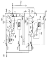
- FIG. 3 is a circuit diagram showing a configuration example of the voltage control unit 1 used in the power supply devices 101 and 102 of FIGS. 1 and 2.
- the voltage control unit 1 includes a reference voltage circuit 11, an arithmetic amplifier circuit 12, a current-voltage conversion circuit 13, a voltage detection circuit 14 including voltage dividing resistors R1 and R2, and P-channel MOS transistors Q1 and Q2. It is configured to include a current mirror circuit CM1 including.
- the reference voltage circuit 11 is a known reference voltage circuit (also referred to as a reference voltage source), generates a predetermined reference voltage Vref based on the input voltage Vin, and outputs it to the inverting input terminal of the arithmetic amplifier circuit 12.
- the input voltage Vin is input to the arithmetic amplifier circuit 12 as a power supply voltage, and is output to the output terminal T13 via the source and drain of the MOS transistor Q1 that controls the output current Iout0 from the voltage control unit 1.
- the output terminals T3 are grounded via voltage dividing resistors R1 and R2 connected in series with each other.
- the output voltage Vout of the output terminal T13 is divided by the voltage dividing resistors R1 and R2 of the voltage detection circuit 14, and the voltage of the voltage dividing resistor R2 after the voltage division (voltage proportional to the output voltage Vout) is calculated as the feedback voltage Vfb. It is input to the inverting input terminal of the amplification circuit 12.
- the arithmetic amplifier circuit 12 outputs the difference voltage between the feedback voltage Vfb and the reference voltage Vref as an output current control signal to each gate (control terminal) of the MOS transistors Q1 and Q2.
- the MOS transistors Q1 and Q2 constitute a current mirror circuit CM1, and in the MOS transistor Q2, a detection current a ⁇ Iout1 proportional to the output current Iout0 flowing through the MOS transistor Q1 is a current-voltage conversion circuit from the source to the drain via the drain.
- the coefficient a is a sufficiently small value (negligible value) as compared with 1, for example, 1 / 10,000, or at least 1/100.
- the current-voltage conversion circuit 13 converts the input detection currents a and Iout1 into a current detection signal BS1 which is an analog voltage signal indicating the detection current, and outputs the current detection signal output terminal T12.
- a reference voltage circuit 11 that generates a reference voltage Vref based on the input voltage Vin, and (2) Based on the input voltage Vin by controlling the output current Iout0 of the voltage control unit 1 by the MOS transistor Q2 so that the output voltage Vout of the voltage control unit 1 becomes a voltage substantially proportional to the reference voltage Vref.
- the voltage control circuit 15 that generates and outputs the output voltage Vout of the voltage control unit 1 and (3) With a current detection circuit (MOS transistor Q2 and current-voltage conversion circuit 13) that detects the output current Iout0 of the voltage control unit 1 and generates and outputs a current detection signal BS1 indicating a value corresponding to the output current Iout0. To be equipped.
- the voltage control unit 1 converts the input voltage Vin into an output voltage Vout proportional to the reference voltage Vref and outputs it, and outputs a current detection signal BS1 indicating a value proportional to the output current Iout0.
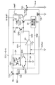
- FIG. 4 is a circuit diagram showing a configuration example of current control units 2,2-1 to 2-N (hereinafter, collectively referred to as reference numerals 2) used in the power supply devices 101 and 102 of FIGS. 1 and 2. ..
- the current control unit 2 includes an arithmetic amplifier circuit 21, a current-voltage conversion circuit 22, and a current mirror circuit CM2 including P-channel MOS transistors Q11 and Q12.
- the input voltage Vin is input to the arithmetic amplifier circuit 21 as a power supply voltage, and is output to the output terminal T23 via the source and drain of the MOS transistor Q11 that controls the output current Iout1 from the voltage control unit 1.
- the MOS transistors Q11 and Q12 constitute a current mirror circuit CM2, and the MOS transistor Q12 has a detection current b ⁇ Iout1 proportional to the output current Iout1 flowing through the MOS transistor Q11, which is a current-voltage conversion circuit from the source to the drain. It flows to 22.
- the coefficient b is a sufficiently small value (negligible value) as compared with 1, for example, 1 / 10,000, or at least 1/100.
- the current-voltage conversion circuit 22 converts the input detection current b ⁇ Iout1 into a current detection signal BS2 which is an analog voltage signal indicating the detection current, and outputs it to the non-inverting input terminal of the arithmetic amplifier circuit 21.
- the coefficient b may be set equal to or different from the coefficient a.
- the arithmetic amplifier circuit 21 outputs the difference voltage signal between the current detection signal BS2 and the current detection signal BS1 as the output current control signal SS1 to the gates (control terminals) of the MOS transistors Q11 and Q12.
- the arithmetic amplification circuit 21, the MOS transistor Q12, and the current-voltage conversion circuit 22 constitute a current control circuit 26 so that the difference voltage between the current detection signal BS2 and the current detection signal BS1 becomes substantially zero. That is, the output current Iout1 is controlled so that the current detection signal BS2 substantially matches the current detection signal BS1.
- the current control circuit 26 sets the output current Iout1 to a predetermined current value (for example, a current value equal to the output current Iout0 of the voltage control unit 1 or proportional to the output current Iout0 of the voltage control unit 1). Control to be.
- a predetermined current value for example, a current value equal to the output current Iout0 of the voltage control unit 1 or proportional to the output current Iout0 of the voltage control unit 1). Control to be.
- a current detection circuit MOS transistor that detects the output current Iout1 of the current control unit 2 and generates and outputs a current detection signal BS2 that is proportional to, for example, the output current Iout1 and indicates a value corresponding to the output current Iout1.
- Q2 and current-voltage conversion circuit 22 (2)
- the current control unit 2 controls the output current Iout1 of the current control unit 2 so that the current detection signal BS2 substantially corresponds to the value indicated by the current detection signal BS1.
- FIG. 5 is a circuit diagram showing a detailed configuration of the power supply device 101 of FIG. The circuit diagram of FIG. 5 is shown so that the voltage control unit 1 of FIG. 3 and the current control unit 2 of FIG. 4 are inserted into the power supply device 101 of FIG.
- the voltage control unit 1 has a closed control loop Lmaster of the voltage control circuit 15 that controls the output voltage Vout.
- the current control unit 2 has a closed control loop L slave of the current control circuit 26 that controls the output current Iout1.
- the respective control loops Lmaster and Lslav can be independently designed to ensure stability and are not complicated. Further, when the response of the closed control loop Lsave does not have a great influence on the response of the closed control loop Lmaster, the phase margin and the gain margin can be determined substantially only by the closed control loop Lmaster.
- FIG. 6 is a circuit diagram showing a configuration example according to the first embodiment of the current control units 2, 2-1 to 2-N (generally referred to by reference numerals 2 in the first embodiment) of FIG.
- the reference numerals of FIG. 3 are used for the output current Iout1 and the detection currents b ⁇ Iout1.
- the current control unit 2 differs from the current control unit 2 in FIG. 4 in the following points.
- (1) A specific example in which the current-voltage conversion circuit 22 is composed of the variable resistor VR1 is shown.
- the voltage at the input end of the current-voltage conversion circuit 22 is output as a monitor voltage Vunitor via the terminal T25.
- (3) The power supply devices 101 and 102 are provided with a current setting controller 4 that controls the variable resistor VR1 based on the monitor voltage Vunitor. The differences will be described below.
- the detection currents b and Iout1 detected by the MOS transistor Q12 are grounded via the variable resistor VR1, and the voltage across the variable resistor VR1 is input to the non-inverting input terminal of the arithmetic amplifier circuit 21 as the current detection signal BS2.
- the variable resistor VR1 inputs the detection current b ⁇ Iout1, converts it into an analog voltage signal using a predetermined transfer impedance, and outputs it as the current detection signal BS2.
- the transfer impedance between the output current Iout1 of the MOS transistor Q11 and the voltage of the current detection signal BS2 applied to the non-inverting input terminal of the arithmetic amplifier circuit 21 is the current ratio b between the MOS transistor Q11 and the MOS transistor Q12. And the absolute value of the resistance value of the variable resistor VR1.
- variable resistor VR1 may have the following forms, for example.
- Form A The variable resistance VR1 is configured to include a plurality of resistance elements connected in series with each other and a switching element connected in parallel with each resistance element, and the variable resistance is formed by turning on or off each switching element. The resistance value of VR1 is changed and set.
- Form B The variable resistance VR1 is configured to include a plurality of resistance elements connected in series with each other and a fuse element connected in parallel with each resistance element, and the variable resistance VR1 is formed by laser trimming each fuse element. The resistance value of is changed and set.
- the transfer impedance between the output current Iout1 of the MOS transistor Q11 and the voltage of the current detection signal BS2 of the current-voltage conversion circuit 22 may deviate from a predetermined value, whereby they are connected in parallel.
- a difference occurs in each output current Iout0 to IoutN of the voltage control unit 1 and each current control unit 2.
- the transfer impedance between the MOS transistor Q11 and the non-inverting input terminal of the math amplifier circuit 21 can be adjusted to a predetermined value, and the voltage can be adjusted. The difference can be reduced in each output current Iout0 to IoutN of the control unit 1 and each current control unit 2.
- Example 1 of FIG. 6 in order to suppress not only the variation of the variable resistor VR1 but also the variation of the transmission impedance, a terminal T25 for measuring the monitor voltage Vunitor corresponding to the transmission impedance is provided.
- the current detection signal BS1 can be used in the current-voltage conversion circuit 13 of the voltage control unit 1 of FIG.
- the current setting controller 4 is provided as a setting circuit for automatically controlling the resistance value of the variable resistor VR1 based on the monitor voltage Vunitor. This automatic control may be performed in real time or may be executed at a predetermined cycle.
- the current setting controller 4 includes a CPU (Central Processing Unit) 41, an EEPROM (Electrically Erasable Programmable Read-Only Memory) 42, an AD converter (ADC) 42, and an interface circuit (I / F) 43. Will be done.
- the EEPROM 41 may be a ROM (Read Only Memory) depending on the usage pattern.
- a variable resistor VR1 is set with respect to the monitor voltage Vunitor according to the set current ratios of the output current Iout0 of the voltage control unit 1 and the output currents Iout1 to IoutN of each current control unit 2 (when they are equal to each other and when they are different).
- the value relation table is stored in advance.
- the AD converter 42 converts the monitor voltage Vunitor into a digital voltage value and outputs it to the CPU 40.
- the CPU 40 searches the relation table in the EEPROM 41 for the set value of the resistance value of the variable resistor VR1 corresponding to the digital voltage value of the input monitor voltage Vunitor, and sets the resistance value of the variable resistor VR1 via the interface circuit 43. do. If the variable resistor VR1 is, for example, the above-described A, the resistance value of the variable resistor VR1 is set to a predetermined value by turning on or off each switching element of the variable resistor VR1.
- the current setting controller 4 can accurately measure the transmission impedance in consideration of the variation of each element described above, and the resistance value of the variable resistor VR1 can be set via the interface circuit 43 so as to adjust the transmission impedance to a predetermined value. As a result, the value of the coefficient b can be changed, and the output current Iout1 of the current control unit 2 can be adjusted and set.
- the current setting controller 4 is set so that the ratio of the output current from the voltage control unit 1 to the output current from each current control unit 2 becomes a predetermined value. Further prepare.
- the variable resistor VR1 divides the detected currents b ⁇ Iout detected by the MOS transistor Q12 at a predetermined current ratio and outputs the current to the arithmetic amplifier circuit 21.
- the current setting controller 4 is used.
- the variable resistor VR1 is configured in the above-described form B without using the current setting controller 4, and is variable by the laser trimming method while, for example, the manufacturer measures the monitor voltage Vunitor with a voltmeter.
- the resistor VR1 may be adjusted and set.
- the transmission impedance is adjusted by the laser trimming method, the resistance value of the variable resistor VR1 is adjusted in the direction of increasing the resistance value. Therefore, the transmission impedance before trimming is set to a value slightly lower than the predetermined value, and by trimming. It is preferable to have a configuration that increases the transfer impedance to a predetermined value.
- variable resistor VR1 may be shipped as a fixed value after being adjusted at the time of manufacture before shipment. Further, when the value of the variable resistor VR1 at the time of design is not different from the resistance value at the time of manufacturing, the variable resistor VR1 may be a fixed resistance.
- FIG. 6 shows a specific example of the current-voltage conversion circuit 22
- the current-voltage conversion circuit 13 of the voltage control unit 1 may be configured in the same manner.
- the current setting controller 4 of FIG. 6 may be configured by a DSP (Digital Signal Processor) or the like.
- FIG. 7 is a circuit diagram showing a configuration example according to a second embodiment of the current control units 2, 2-1 to 2-N (generally referred to as reference numerals 2 in the second embodiment) of FIG.
- the reference numerals of FIG. 3 are used for the output current Iout1 and the detection currents b ⁇ Iout1.
- the current control unit 2 according to the second embodiment is different from the current control unit 2 in FIG. 6 in the following points.
- (1) A specific example in which the current-voltage conversion circuit 22 is composed of the variable resistors VR1 and VR2 is shown.
- (2) instead of the current setting controller 4, a current setting controller 4A provided with an interface circuit 44 capable of controlling the variable resistor VR2 is provided. The differences will be described below.
- the current-voltage conversion circuit 22 and the detection current b ⁇ Iout1 detected by the MOS transistor Q12 are input, and the current detection signal BS2, which is an analog voltage signal, is converted into an arithmetic amplifier circuit using a predetermined transfer impedance.
- the transfer impedance between the output current Iout1 of the MOS transistor Q11 and the voltage of the current detection signal BS2 input to the non-inverting input terminal of the arithmetic amplifier circuit 21 is the current ratio b of the MOS transistor Q11 and the MOS transistor Q12. It can be determined by the voltage division ratio of the variable resistors VR1 and VR2 and the absolute value thereof.
- the current setting controller 4A can accurately measure the transmission impedance in consideration of the variation of each element described above, and adjusts the resistance values of the variable resistors VR1 and VR2 to a predetermined value via the interface circuits 43 and 44. Can be set. As a result, the value of the coefficient b can be changed, and the output current Iout1 of the current control unit 2 can be adjusted and set.
- the current setting controller 4 is set so that the ratio of the output current from the voltage control unit 1 to the output current from each current control unit 2 becomes a predetermined value. Further prepare.
- the variable resistors VR1 and VR2 divide the detection current b ⁇ Iout detected by the MOS transistor Q12 at a predetermined voltage division ratio and divide the current at a predetermined current ratio to output to the arithmetic amplifier circuit 21.
- Example 2 Note that the modified example of Example 1 can be similarly applied to Example 2.
- FIG. 8 is a circuit diagram showing a configuration example according to a third embodiment of the current control units 2, 2-1 to 2-N of FIG. 4 (generally referred to with reference numerals 2 in the third embodiment).
- the output current Iout1 and the detection currents b ⁇ Iout1 use the reference numerals of FIG.
- the current control unit 2 differs from the current control unit 2 of FIG. 4 in the following points.
- the arithmetic amplifier circuit 21 is a known arithmetic amplifier circuit, and includes four MOS transistors Q21 to Q24 and a constant current source 24, which is a so-called tail current source.
- An arithmetic amplifier circuit 23 for switching on / off of the MOS transistor Q13 is provided. The differences will be described below.
- the third embodiment of FIG. 8 provides a circuit configuration for improving the responsiveness of the power supply devices 101 and 102.
- the input voltage Vin is input to the math amplifier circuit 23 as the power supply voltage, and the voltage of the current detection signal BS1 is input to each inverting input terminal of the math amplifier circuits 21 and 23. Further, the voltage of the current detection signal BS2 of the current-voltage conversion circuit 22 is input to the non-inverting input terminal of the arithmetic amplifier circuit 23.
- the math amplifier circuit 23 generates a switch control signal SS2 according to the two input signal voltages and outputs the switch control signal SS2 to the gate of the MOS transistor Q13.
- the arithmetic amplifier circuit 23 when the voltage of the current detection signal BS1 becomes equal to or lower than a predetermined threshold value, the arithmetic amplifier circuit 23 outputs a switch control signal for turning on the MOS transistor Q13 to the gate of the MOS transistor Q13. As a result, the responsiveness of the output current Iout1 is improved by supplying the MOS transistor Q11 with a constant current from the constant current source 25 operated by the input voltage Vin.
- the MOS transistor Q13 is turned on when the voltage of the current detection signal BS1 becomes equal to or lower than a predetermined threshold value, that is, when the output current Iout1 of the current control unit 2 exceeds the output current Iout0 of the voltage control unit 1.
- a predetermined threshold value that is, when the output current Iout1 of the current control unit 2 exceeds the output current Iout0 of the voltage control unit 1.
- the response characteristics of the voltage control unit 1 and the current control unit 2 are not the same, and the response when switching from a heavy load to a light load due to the characteristic of the slower response is obtained. Since sex is determined, it is important to improve the characteristics of the slower response when improving this. At that time, if the response of the current control unit 2 is slower than that of the voltage control unit 1, the circuit of FIG. 8 for improving the response of the current control unit 2 is required.
- a constant current source 25 that generates a predetermined constant current based on the input voltage Vin
- a MOS transistor Q11 which is a current control element that includes a gate (control terminal) for inputting the output current control signal SS1 and controls the output current Iout1 from the current control unit 2 based on the output current control signal SS1.
- a MOS transistor Q13 which is a switch element for inputting the constant current to the gate of the MOS transistor Q11 when the current detection signal SS2 becomes equal to or lower than a predetermined threshold value, is provided.
- Example 3 may be applied to Example 1 or 2.
- the current detection signal BS1 in which the voltage control unit 1 and each current control unit 2 are connected in parallel to each other and a part of the output current Iout0 of the voltage control unit 1 is detected. Is transmitted to each current control unit 2, and each current control unit is based on the difference signal between the current detection signal BS1 and the current detection signal BS2 that detects a part of the output currents Iout1 to IoutN of each current control unit 2. It was configured to control the output currents Iout1 to IoutN of 2. As a result, as shown in FIG.
- the voltage control unit 1 has only the closed control loop Lmaster that controls the output voltage Vout, and each current control unit 2 has only the closed control loop Lslav that controls the output currents Iout1 to IoutN. Have. Therefore, the feedback control loops are not mixed in the internal circuits of the power supply devices 101 and 102, the configurations of the voltage control unit 1 and each current control unit 2 are not the same, and each response frequency can be separated. Loss of stability due to resonance can be prevented.
- each current control unit 2 can realize characteristics different from the response frequency of the voltage control unit 1, and each response frequency can be separated. This can prevent the loss of stability due to the resonance of each response.
- the offset voltage Voffset (FIG. 8) of the arithmetic amplifier circuit 23 that compares the output current detection signal BS1 with the current detection signal BS2 becomes larger than a predetermined value
- the current detection signal BS1 of the voltage control unit 1 and each current control unit 2 , BS2 difference signal is generated, and a difference occurs in the output current amount.
- the amplification factor of the output current detection signal BS1 is increased, the sensitivity of the offset voltage Voffset of the arithmetic amplifier circuit 23 to the current difference is lowered, and the design in the CMOS circuit is facilitated, so that the configuration is lower in consumption. It is possible to realize a control system with.
- the control system of the voltage control unit and the control system of each current control unit can be separated, so that the control system is stable as compared with the prior art. It is possible to provide a power supply device or the like that can prevent unnecessary oscillation by establishing a control system.
- An electronic device may be configured by including the power supply devices 101 and 102 according to the embodiment and the load 3.
- Electronic devices include, for example, electronic devices for automobiles that receive power supply, image forming devices such as copiers or printers that receive power supply, personal computers, tablets, smart phones, mobile phones, and the like.
Landscapes
- Engineering & Computer Science (AREA)
- Physics & Mathematics (AREA)
- Electromagnetism (AREA)
- General Physics & Mathematics (AREA)
- Radar, Positioning & Navigation (AREA)
- Automation & Control Theory (AREA)
- Continuous-Control Power Sources That Use Transistors (AREA)
Priority Applications (4)
| Application Number | Priority Date | Filing Date | Title |
|---|---|---|---|
| JP2022508720A JP7170935B2 (ja) | 2020-03-18 | 2020-03-18 | 電源装置及び電子機器 |
| CN202080042715.7A CN114008555B (zh) | 2020-03-18 | 2020-03-18 | 电源装置以及电子设备 |
| PCT/JP2020/012082 WO2021186635A1 (ja) | 2020-03-18 | 2020-03-18 | 電源装置及び電子機器 |
| US17/595,941 US11853093B2 (en) | 2020-03-18 | 2020-03-18 | Power supply device provided with voltage controller using reference voltage circuit and current controller, and electronic apparatus with the power supply device |
Applications Claiming Priority (1)
| Application Number | Priority Date | Filing Date | Title |
|---|---|---|---|
| PCT/JP2020/012082 WO2021186635A1 (ja) | 2020-03-18 | 2020-03-18 | 電源装置及び電子機器 |
Publications (1)
| Publication Number | Publication Date |
|---|---|
| WO2021186635A1 true WO2021186635A1 (ja) | 2021-09-23 |
Family
ID=77768436
Family Applications (1)
| Application Number | Title | Priority Date | Filing Date |
|---|---|---|---|
| PCT/JP2020/012082 Ceased WO2021186635A1 (ja) | 2020-03-18 | 2020-03-18 | 電源装置及び電子機器 |
Country Status (4)
| Country | Link |
|---|---|
| US (1) | US11853093B2 (https=) |
| JP (1) | JP7170935B2 (https=) |
| CN (1) | CN114008555B (https=) |
| WO (1) | WO2021186635A1 (https=) |
Cited By (1)
| Publication number | Priority date | Publication date | Assignee | Title |
|---|---|---|---|---|
| JP2024007633A (ja) * | 2022-07-06 | 2024-01-19 | ローム株式会社 | 電源システム |
Families Citing this family (2)
| Publication number | Priority date | Publication date | Assignee | Title |
|---|---|---|---|---|
| CN116301181B (zh) * | 2023-05-16 | 2023-07-21 | 上海灵动微电子股份有限公司 | 低压差线性稳压器负载跳变的过冲抑制电路 |
| WO2025041267A1 (ja) * | 2023-08-22 | 2025-02-27 | 日清紡マイクロデバイス株式会社 | 電源装置及び電子機器 |
Citations (3)
| Publication number | Priority date | Publication date | Assignee | Title |
|---|---|---|---|---|
| JPS6032566A (ja) * | 1983-08-03 | 1985-02-19 | Nec Corp | 入力監視回路 |
| JP2008109736A (ja) * | 2006-10-23 | 2008-05-08 | Murata Mfg Co Ltd | 電源システム |
| JP2010049482A (ja) * | 2008-08-21 | 2010-03-04 | Sharp Corp | 直流安定化電源装置 |
Family Cites Families (10)
| Publication number | Priority date | Publication date | Assignee | Title |
|---|---|---|---|---|
| JPS6032566B2 (ja) | 1978-07-07 | 1985-07-29 | カネボウ株式会社 | セメント製品の型枠成型方法 |
| JP3453039B2 (ja) | 1997-03-18 | 2003-10-06 | シャープ株式会社 | 直流安定化電源 |
| CN1716142A (zh) * | 2004-06-14 | 2006-01-04 | 罗姆股份有限公司 | 具有过电流保护功能的电源装置 |
| JP2007334761A (ja) * | 2006-06-16 | 2007-12-27 | Rohm Co Ltd | 電圧生成回路及びそれを備えた電源回路 |
| JP5014194B2 (ja) * | 2008-02-25 | 2012-08-29 | セイコーインスツル株式会社 | ボルテージレギュレータ |
| JP6180815B2 (ja) * | 2013-06-21 | 2017-08-16 | エスアイアイ・セミコンダクタ株式会社 | ボルテージレギュレータ |
| WO2017094402A1 (ja) * | 2015-11-30 | 2017-06-08 | 株式会社村田製作所 | スイッチング電源装置及び誤差補正方法 |
| US10211486B2 (en) * | 2017-02-03 | 2019-02-19 | QDroid Inc. | Battery with built-in wireless communication |
| US10627842B2 (en) * | 2018-06-18 | 2020-04-21 | Analog Devices Global Unlimited Company | Lossless current balancing and sharing between paralleled linear voltage regulators |
| US10599171B2 (en) * | 2018-07-31 | 2020-03-24 | Analog Devices Global Unlimited Company | Load-dependent control of parallel regulators |
-
2020
- 2020-03-18 WO PCT/JP2020/012082 patent/WO2021186635A1/ja not_active Ceased
- 2020-03-18 US US17/595,941 patent/US11853093B2/en active Active
- 2020-03-18 JP JP2022508720A patent/JP7170935B2/ja active Active
- 2020-03-18 CN CN202080042715.7A patent/CN114008555B/zh active Active
Patent Citations (3)
| Publication number | Priority date | Publication date | Assignee | Title |
|---|---|---|---|---|
| JPS6032566A (ja) * | 1983-08-03 | 1985-02-19 | Nec Corp | 入力監視回路 |
| JP2008109736A (ja) * | 2006-10-23 | 2008-05-08 | Murata Mfg Co Ltd | 電源システム |
| JP2010049482A (ja) * | 2008-08-21 | 2010-03-04 | Sharp Corp | 直流安定化電源装置 |
Cited By (1)
| Publication number | Priority date | Publication date | Assignee | Title |
|---|---|---|---|---|
| JP2024007633A (ja) * | 2022-07-06 | 2024-01-19 | ローム株式会社 | 電源システム |
Also Published As
| Publication number | Publication date |
|---|---|
| JP7170935B2 (ja) | 2022-11-14 |
| CN114008555A (zh) | 2022-02-01 |
| JPWO2021186635A1 (https=) | 2021-09-23 |
| CN114008555B (zh) | 2022-11-22 |
| US20220221889A1 (en) | 2022-07-14 |
| US11853093B2 (en) | 2023-12-26 |
Similar Documents
| Publication | Publication Date | Title |
|---|---|---|
| US6498469B2 (en) | Internal supply voltage generating circuit and method of generating internal supply voltage using an internal reference voltage generating circuit and voltage-drop regulator | |
| US7696793B2 (en) | Driver circuit and method for differential signaling with improved signal level control | |
| US9298200B2 (en) | Constant voltage circuit with drooping and foldback overcurrent protection | |
| US7368896B2 (en) | Voltage regulator with plural error amplifiers | |
| US8044653B2 (en) | Low drop-out voltage regulator | |
| US7893671B2 (en) | Regulator with improved load regulation | |
| US9874887B2 (en) | Voltage regulator with adjustable feedback | |
| US6535408B2 (en) | Power converter with adjustable output voltage | |
| JP2023041853A (ja) | レギュレータ装置 | |
| US9411345B2 (en) | Voltage regulator | |
| JP7170935B2 (ja) | 電源装置及び電子機器 | |
| JP7223225B2 (ja) | 電源制御用半導体装置および出力電圧可変電源装置 | |
| US20050088154A1 (en) | Voltage regulator | |
| CN116430937A (zh) | 一种具有多模式的低压差线性稳压器及其控制方法 | |
| US12535841B2 (en) | Regulator circuit for parallel configuration and user device including the same | |
| US10186969B2 (en) | Semiconductor device | |
| US11025234B1 (en) | Process and temperature compensated ring oscillator | |
| CN103380383B (zh) | 用于较宽电流感测范围的合成电流感测电阻器 | |
| US7245146B2 (en) | Semiconductor device with termination resistance adjusting circuit | |
| US8149063B2 (en) | Current-restriction circuit and driving method therefor | |
| KR101796769B1 (ko) | 캡리스 로우 드랍 아웃 레귤레이터 및 그 제어 회로 | |
| US20260126822A1 (en) | Regulator circuit for parallel configuration and user device including the same | |
| CN223219008U (zh) | 装置和集成电路芯片 | |
| CN107078704B (zh) | 用于跨导放大器的调节装置 | |
| JP2005190265A (ja) | 定電圧電源回路 |
Legal Events
| Date | Code | Title | Description |
|---|---|---|---|
| 121 | Ep: the epo has been informed by wipo that ep was designated in this application |
Ref document number: 20926179 Country of ref document: EP Kind code of ref document: A1 |
|
| ENP | Entry into the national phase |
Ref document number: 2022508720 Country of ref document: JP Kind code of ref document: A |
|
| NENP | Non-entry into the national phase |
Ref country code: DE |
|
| 122 | Ep: pct application non-entry in european phase |
Ref document number: 20926179 Country of ref document: EP Kind code of ref document: A1 |