WO2025041267A1 - 電源装置及び電子機器 - Google Patents
電源装置及び電子機器 Download PDFInfo
- Publication number
- WO2025041267A1 WO2025041267A1 PCT/JP2023/030164 JP2023030164W WO2025041267A1 WO 2025041267 A1 WO2025041267 A1 WO 2025041267A1 JP 2023030164 W JP2023030164 W JP 2023030164W WO 2025041267 A1 WO2025041267 A1 WO 2025041267A1
- Authority
- WO
- WIPO (PCT)
- Prior art keywords
- current
- voltage
- control unit
- output
- power supply
- Prior art date
- Legal status (The legal status is an assumption and is not a legal conclusion. Google has not performed a legal analysis and makes no representation as to the accuracy of the status listed.)
- Pending
Links
Images


Classifications
-
- G—PHYSICS
- G05—CONTROLLING; REGULATING
- G05F—SYSTEMS FOR REGULATING ELECTRIC OR MAGNETIC VARIABLES
- G05F1/00—Automatic systems in which deviations of an electric quantity from one or more predetermined values are detected at the output of the system and fed back to a device within the system to restore the detected quantity to its predetermined value or values, i.e. retroactive systems
- G05F1/10—Regulating voltage or current
- G05F1/46—Regulating voltage or current wherein the variable actually regulated by the final control device is DC
- G05F1/56—Regulating voltage or current wherein the variable actually regulated by the final control device is DC using semiconductor devices in series with the load as final control devices
-
- H—ELECTRICITY
- H02—GENERATION; CONVERSION OR DISTRIBUTION OF ELECTRIC POWER
- H02M—APPARATUS FOR CONVERSION BETWEEN AC AND AC, BETWEEN AC AND DC, OR BETWEEN DC AND DC, AND FOR USE WITH MAINS OR SIMILAR POWER SUPPLY SYSTEMS; CONVERSION OF DC OR AC INPUT POWER INTO SURGE OUTPUT POWER; CONTROL OR REGULATION THEREOF
- H02M3/00—Conversion of DC power input into DC power output
Definitions
- the present invention relates to a power supply device that includes, for example, a voltage control unit that is a linear regulator using a reference voltage generation circuit, and at least one current control unit, and to an electronic device that includes the power supply device.
- the output voltage begins to drop, so when the load current is above a certain level and the output setting voltage falls below the output setting voltage of the lower linear regulator, this regulator will begin to supply output current.
- the output current supply balance is uneven, and the linear regulator with the lower output setting voltage cannot supply an output current equal to that of the other linear regulator, so there is a possibility that the required load current value will not be met.
- an imbalance in the output currents will also cause an imbalance in heat generation, accelerating the lifespan of the linear regulator with the highest output current and threatening to destroy it.
- each linear regulator detects its own output current, converts it into an analog voltage signal, and outputs the voltage signal information from one linear regulator via each bus terminal, then inputs the voltage signal information to the other linear regulator and compares the respective voltage signals, thereby keeping the output currents of the two linear regulators equal.
- the object of the present invention is to provide a power supply device that can solve the above problems and prevent the output voltage from rising when there is no load or a light load, and an electronic device equipped with the power supply device.
- a power supply device includes: A power supply device including a voltage control unit and a current control unit, the voltage control unit and the current control units being connected in parallel to each other,
- the voltage control unit is a reference voltage circuit that generates a predetermined reference voltage based on an input voltage; a voltage control circuit that generates and outputs an output voltage of the voltage control unit based on the input voltage by controlling an output current of the voltage control unit so that the output voltage of the voltage control unit becomes a voltage that substantially corresponds to the reference voltage
- the current control unit is a first current detection circuit that detects an output current of the current control unit and generates and outputs a first current detection signal indicating a value corresponding to the output current; a current control circuit that controls an output current of the current control unit so that the first current detection signal has a value that substantially corresponds to the output current of the voltage control unit;
- the power supply includes an activation control circuit that activates the current control circuit to cause the output current of the current control circuit to flow when the output current of the voltage control section
- a power supply device when there is no load or a light load, it is possible to prevent the output voltage from rising to the input voltage, and thus to prevent the output voltage from rising.
- FIG. 1 is a circuit diagram showing a configuration example of a power supply device according to a first embodiment.
- FIG. 4 is a circuit diagram showing a detailed configuration example of a power supply device according to a modified example of the first embodiment.
- 3 is a timing chart of currents and voltages illustrating the operation of the power supply device of FIG. 2 .
- FIG. 11 is a circuit diagram showing a configuration example of a power supply device according to a second embodiment.
- FIG. 11 is a circuit diagram showing a configuration example of a power supply device according to a third embodiment.
- FIG. 13 is a circuit diagram showing a configuration example of a power supply device according to a fourth embodiment.
- FIG. 13 is a circuit diagram showing a configuration example of a power supply device according to a fifth embodiment.
- FIG. 13 is a circuit diagram showing a configuration example of a power supply device according to a sixth embodiment. 9 is a timing chart of currents and voltages illustrating the operation of the power supply device of FIG. 8 .
- FIG. 13 is a circuit diagram showing a configuration example of a power supply device according to a seventh embodiment. 11 is a timing chart of currents and voltages illustrating the operation of the power supply device of FIG. 10.
- FIG. 13 is a circuit diagram showing a configuration example of a power supply device according to an eighth embodiment. 13 is a graph showing the relationship between each voltage and offset voltage Voffset with respect to output current Iot in the power supply device of FIG. 12. 13 is a graph showing output currents Io1 and Io2 in the power supply device of FIG.
- FIG. 13 is a graph showing output currents Io1 and Io2 in the power supply device of FIG. 12 when no offset voltage is intentionally applied, relative to the output current Iot.
- FIG. 13 is a circuit diagram showing a configuration example of a power supply device according to a ninth embodiment.
- 15 is a graph showing the relationship of the current flowing into the current-voltage conversion circuit with respect to the output current Iot in the power supply device of FIG. 14 .
- FIG. 23 is a circuit diagram showing a configuration example of a power supply device according to a tenth embodiment. 17 is a timing chart showing current and voltage in the power supply device of FIG. 16 .
- FIG. 1 is a block diagram showing a configuration of a power supply device according to a comparative example.
- FIG. 18 is a block diagram showing the configuration of a power supply device 61 according to a comparative example disclosed in Patent Document 1.
- the power supply device 61 is configured to include a voltage control unit 1 and a current control unit 2.
- the input terminal T11 of the voltage control unit 1 and the input terminal T21 of the current control unit 2 are connected to each other and to a voltage source of the input voltage Vin.
- the output terminal T13 of the voltage control unit 1 and the output terminal T23 of the current control unit 2 are connected to each other and to a load 3.
- the voltage control unit 1 and the current control unit 2 are connected in parallel to each other.
- the current detection signal output terminal T12 of the voltage control unit 1 and the current detection signal input terminal T22 of the current control unit 2 are connected to each other, and the ground terminal T14 of the voltage control unit 1 and the ground terminal T24 of the current control unit 2 are connected to each other and grounded.
- IN indicates the input terminal of the input voltage
- OUT indicates the output terminal
- BSout indicates the output terminal of the current detection signal BS1
- BSin indicates the input terminal of the current detection signal BS
- GND indicates the ground terminal.
- the input voltage Vin is input to the input terminal T11 of the voltage control unit 1 and the input terminal T21 of the current control unit 2.
- the voltage control unit 1 is a linear regulator with a built-in reference voltage generation circuit, and controls the input voltage Vin to be the reference voltage.
- a total current Iouttotal which is the sum of the output current Iout0 from the voltage control unit 1 and the output current Iout1 from the current control unit 2, flows to the load 3.
- the voltage control unit 1 also generates a current detection signal BS1, which is an analog voltage signal that corresponds to the output current Iout0 with a predetermined correlation, such as being proportional, and outputs it from the current detection signal output terminal T12 to the current detection signal input terminal T22 of the current control unit 2.
- the current control unit 2 generates a current detection signal, which is an analog voltage signal that corresponds to the output current Iout1 with a predetermined correlation, such as being proportional, and compares the current detection signal with the input current detection signal BS1 to control the difference to be substantially zero, that is, the impedance of the output transistor (e.g., corresponding to the MOS transistor Q11 in FIG. 1) that controls the output current Iout1 of the current control unit 2 is controlled so that the output current Iout0 and the output current Iout1 are, for example, equal to each other.
- the output current Iout0 and the output current Iout1 are, for example, equal to each other.
- the load 3 is, for example, an electronic device having a predetermined function that receives the power supply voltage and power supply current from the voltage control unit 1 and the current control unit 2.
- the load 3 is an electronic device for an automobile that receives power supply, or an image forming device such as a copier or printer that receives power supply, a personal computer, a tablet, a smartphone, a mobile phone, etc.
- the voltage control system in the voltage control unit 1 and the current control system in the current control unit 2 are separate, so they do not affect each other. Therefore, it is possible to realize a power supply device 61 that can establish a stable control system compared to the prior art and prevent unnecessary oscillations.
- the slave side current control unit 2 that receives the current information flows more current than the master side voltage control unit 1 that outputs the current information, the slave side current control unit 2 flows current even though the master side voltage control unit 1 tries to control the current to stop when there is no load, and the output voltage Vout rises to the input voltage Vin.
- the purpose of the embodiments of the present invention is to provide a power supply device that can solve the above problems and prevent the output voltage from rising when there is no load or a light load, and an electronic device equipped with the power supply device.
- a power supply device that can solve the above problems and prevent the output voltage from rising when there is no load or a light load, and an electronic device equipped with the power supply device.
- FIG. 1 is a circuit diagram showing an example of the configuration of a power supply device 51 according to the first embodiment.
- the power supply device 51 is configured to include a voltage control unit 101 and a current control unit 201.
- the input terminal P1 (IN) of the voltage control unit 101 and the input terminals P2 (IN) of the current control unit 201 are connected to each other and to a voltage source of the input voltage Vin.
- the output terminal P2 (OUT) of the voltage control unit 101 and the output terminal P12 (OUT) of the current control unit 201 are connected to each other and to a load 301.
- the voltage control unit 101 and the current control unit 201 are connected in parallel to each other.
- the output terminal P4 (BSmout) that outputs the current detection signal (current I3) of the voltage control unit 101 and the input terminal P14 (BSmin) that inputs the current detection signal (current I3) of the current control unit 102 are connected to each other.
- the output terminal P5 (BSout) that outputs the current-voltage conversion signal (converted voltage V13) of the voltage control unit 101 and the input terminal P15 (BSin) that inputs the current-voltage conversion signal (converted voltage V13) of the current control unit 102 are connected to each other.
- the ground terminal P3 of the voltage control unit 101 and the ground terminal P13 of the current control unit 201 are connected to each other and grounded.
- the input voltage Vin is input to the input terminal P1 of the voltage control unit 101 which constitutes a reference voltage linear regulator that determines the output voltage Vout, and is also input to the input terminal P11 of the current control unit 201.
- the output current Io1 from the output terminal P2 of the voltage control unit 101 and the output current Io2 from the output terminal P12 of the current control unit 201 are added together, and then the added current Iot flows to the load 301.
- An analog current detection signal (current I3) which is detected in the voltage control unit 101 and has a correlation with the output current Io1 and corresponds, for example, in a proportional relationship, is input to the current control unit 201 via the output terminal P4 and the input terminal P14 of the current control unit 201.
- the current control unit 201 generates a current-voltage conversion signal (converted voltage V23) that has a correlation with the output current Io2 of the current control unit 201 and corresponds, for example, in a proportional relationship, and by comparing the current-voltage conversion signal (converted voltage V13) of the voltage control unit 101 with the current-voltage conversion signal (converted voltage V23) of the current control unit 201, the impedance of the output transistor Q11 of the current control unit 201 is controlled so that the output current Io1 and the output current Io2 are equal to each other.
- the current-voltage conversion signal is an example of a current detection signal, and the same applies in the following specification.
- the voltage control unit 101 is a reference voltage linear regulator and is configured with a reference voltage generation circuit 11, an operational amplifier circuit 12, a current-voltage conversion circuit 13, PMOS transistors Q1 to Q3, and voltage-dividing resistors R1 and R2.
- the reference voltage generation circuit 11 generates a predetermined reference voltage Vref based on the input voltage Vin and outputs it to the inverting input terminal of the operational amplifier circuit 12.
- the operational amplifier circuit 12 subtracts the reference voltage Vref from the feedback voltage Vfb divided by the voltage-dividing resistors R1 and R2, amplifies the result, and outputs the amplified error voltage V12 to the gates of the PMOS transistors Q1 to Q3.
- the PMOS transistor Q1 controls the output current I1 generated from the input voltage Vin based on the error voltage V12, generates the output current Io1, and outputs it from the output terminal P2 to the load 301.
- the current-voltage conversion circuit 13 converts the detection current I2 into a corresponding, for example, proportional detection voltage, and outputs it to the input terminal P15 of the current control unit 201 via the output terminal P5 as a current-voltage conversion signal (conversion voltage V13).
- the voltage-dividing resistors R1 and R2 divide the output voltage Vout generated by the output current Io1 into a feedback voltage Vfb, which is output to the non-inverting input terminal of the operational amplifier circuit 12.
- a feedback control circuit (voltage control circuit) consisting of the operational amplifier circuit 12, PMOS transistor Q1, and voltage dividing resistors R1 and R2 controls the output current I1 of the output transistor, PMOS transistor Q1, so that the divided voltage Vfb becomes the reference voltage Vref.
- the current control section 201 is configured with an operational amplifier circuit 21, a current detection circuit 22, a current-voltage conversion circuit 23, and PMOS transistors Q11 and Q12.
- the operational amplifier circuit 21 subtracts the current-voltage conversion signal (conversion voltage V13) from the current-voltage conversion signal (conversion voltage V23) from the current-voltage conversion circuit 23, amplifies the result, and outputs the error voltage V21 to the gates of the PMOS transistors Q11 and Q12.
- the PMOS transistor Q11 controls the output current I11 generated from the input voltage Vin based on the error voltage V21, generates the output current Io2, and outputs it from the output terminal P12 to the load 301.
- the current-voltage conversion circuit 23 converts the detection current I12 into a corresponding, for example proportional, detection voltage and outputs it to the non-inverting input terminal of the operational amplifier circuit 21 as a current-voltage conversion signal (converted voltage V23).
- the current detection circuit 22 When the current I3 input to the input terminal P14 is less than a predetermined third threshold current, the current detection circuit 22 generates an L-level current detection signal S22 and outputs it to the start-up control terminal of the operational amplifier circuit 21 as a non-start-up signal, while when the current I3 is equal to or greater than the third threshold current (i.e., when the output current I1 is equal to or greater than the predetermined first threshold current), it generates an H-level current detection signal S22 and outputs it to the start-up control terminal of the operational amplifier circuit 21 as a start-up signal, thereby starting up the current control circuit including the operational amplifier circuit 21 and controlling it to flow the output current of the current control unit.
- the operational amplifier circuit 21 starts up in response to
- the current detection circuit 22 is an example of a start-up control circuit.
- the start-up signal and the non-start-up signal are collectively called a start-up control signal.
- the start-up control signal is a signal generated by the start-up control circuit.
- a feedback control circuit (current control circuit) consisting of the current detection circuit 22, PMOS transistor Q12, and current-voltage conversion circuit 23 controls the output current I11 of the PMOS transistor Q11, which is an output transistor, so that the output currents Io1 and Io2 are equal to each other.
- the output current Io1 from the voltage control unit 101 and the output current Io2 from the current control unit 201 are generally set to be substantially the same.
- an offset voltage Voff is added to the operational amplifier circuit 21 due to manufacturing variations (hereinafter referred to as the first case), or if a systematic offset voltage is generated due to a predetermined gain of the feedback control circuit in the current control unit 201 (hereinafter referred to as the second case), the output currents Io1 and Io2 will no longer be substantially the same.
- the output current difference ⁇ I of the output transistors Q1 and Q11 with respect to the offset voltage Voff generated in the operational amplifier circuit 21 is expressed by the following equation.
- the current control unit 201 is provided with a current detection circuit 22, and the current detection circuit 22 controls the operational amplifier circuit 21 not to start when the output current I3 corresponding to the current I1 is less than the third threshold current. Therefore, even if an offset voltage Voff is added to the operational amplifier circuit 21, it is possible to prevent the output voltage Vout from increasing.
- the driving state of the master side voltage control unit 101 can be monitored, and the current output of the slave side current control unit 201 can be controlled to be suppressed as necessary, thereby preventing the output voltage Vout from rising to the input voltage Vin.
- the output of the output current Io2 of the slave side current control unit 201 can be stopped, thereby preventing the output voltage Vout from rising.
- the output current Io2 of the current control unit 2 is controlled so that the output current Io1 of the voltage control unit 1 and the output current Io2 of the current control unit 2 are substantially equal to each other.
- the output current Io2 of the current control unit 2 may be controlled by current dispersion so that the ratio between the output current Io1 of the voltage control unit 1 and the output current Io2 of the current control unit 2 is a predetermined value.
- FIG. 2 is a circuit diagram showing a detailed configuration example of a power supply device 51A according to a modification of the first embodiment, and Fig. 2 shows a detailed configuration example of a current detection circuit 22. Note that differences from Fig. 1 will be described below.
- the current detection circuit 22 is configured to include a diode-connected NMOS transistor Q13, a comparator 221, and a reference voltage generation circuit 222.
- A3 is a current-voltage conversion coefficient.
- the current I3 input to the input terminal P14 is grounded via the drain and source of the NMOS transistor Q13 and converted to a corresponding voltage V3, and the converted voltage V3 is applied to the non-inverting input terminal of the comparator 221.
- the comparator 221 compares the converted voltage V3 with the reference voltage Vref2 from the reference voltage generating circuit 222, and when V3 ⁇ Vref2, generates an L-level current detection signal S22 and outputs it to the start-up control terminal of the operational amplifier circuit 21 as a non-start-up signal, while when V3 ⁇ Vref2, generates an H-level current detection signal S22 and outputs it to the start-up control terminal of the operational amplifier circuit 21 as a start-up signal.
- the current detection signal S22 from the comparator 221 is input to the control terminal of the switch SW2 and is also input to the control terminal of the switch SW1 via the inverter INV1.
- the switches SW1 and SW2 are turned on when an H-level control signal is input to their control terminals, while they are turned off when an L-level control signal is input.
- the comparator 221 and the reference voltage generating circuit 222 are an example of a switching control circuit.
- the current control unit 201 configured as above, as the current I3 of the PMOS transistor Q3, which is the monitor transistor, increases, the drain voltage V3 of the diode-connected NMOS transistor Q13 rises. In order to detect the rise in voltage V3, the comparator 221 compares this voltage V3 with the reference voltage Vref2 of the reference voltage generating circuit 222 to generate a current detection signal S22.
- the NMOS transistor Q13 may be replaced with a series circuit of a resistor and a bias current source.
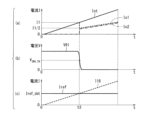
- FIG. 3 is a timing chart of currents and voltages showing the operation of the power supply device 51A in FIG. 2. The operation of the power supply device 51A in FIG. 2 will be described below with reference to FIG. 3.
- the current control unit 201 When the current control unit 201 starts at time t1 in FIG. 3, the current control unit 201 shares half of the total output current Iot (see FIG. 3(a)), and the converted voltage V13 from the current-voltage conversion circuit 13 drops. At this time, the currents Io1 and Io2 of the output transistors Q1 and Q11 are roughly the same as each other and are divided into about half of the total output current Iot, so the current I3 of the monitor transistor Q3 becomes about half of its maximum value (see FIG. 3(b)). At this time, if the threshold current Irel for the current I3 that disables the current control unit 201 is not less than half the startup detection threshold current Idet of the current control unit 201, the current control unit 201 will be disabled again.
- a hysteresis characteristic is provided so that the release threshold current Irel is less than half the startup detection threshold current Idet.
- the current detection signal S22 of the comparator 221 is used to selectively switch between the voltage sources 223 and 224, thereby selectively switching between starting and stopping the current control unit 201 with a predetermined hysteresis characteristic. This prevents unintentional release of the current control unit 201 after it has been started, thereby preventing oscillations such as chattering caused by repeated starting and stopping.
- Fig. 4 is a circuit diagram showing an example of the configuration of a power supply device 52 according to embodiment 2.
- the power supply device 52 according to embodiment 2 differs from the power supply device 51 of Fig. 1 in the following points.
- a current control unit 201A is provided instead of the current control unit 201.
- a current detection circuit 22A is provided instead of the current detection circuit 22.
- the current detection circuit 22A includes a diode-connected NMOS transistor Q14 that serves as a monitor transistor, a comparator 221, and a reference voltage generation circuit 225.
- the reference voltage generation circuit 225 generates a predetermined reference voltage Vref3 and outputs it to the inverting input terminal of the comparator 221.
- the current control section 201A further includes a PMOS transistor Q13 which is a monitor transistor.
- the source of the PMOS transistor Q13 is connected to the input terminal P11, and the gate of the PMOS transistor Q13 is connected to the output terminal of the operational amplifier circuit 21.
- the detection target of the current detection circuit 22A is the current value obtained by adding the current I13 corresponding to the output current I11 of the current control section 201A to the current I3, and the NMOS transistor Q14 converts this current value into a voltage and applies it to the non-inverting input terminal of the comparator 221.
- the current detection circuit 22A is an example of a startup control circuit.
- the power supply device 52 configured as described above, when the current control section 201A is started, the current control section 201 is responsible for generating half of the output current Io1 of the voltage control section 101, so the detection current of the monitor transistor Q3 in FIG. 1 decreases. However, since the sum of the output current Io1 of the voltage control section 101 and the output current Io2 of the current control section 201 does not change, the detection current value of the monitor transistor Q14 does not change from the detection current value of the monitor transistor Q3 before the current control section 201A was started. Therefore, the power supply device 52 according to the second embodiment has the same effect as the power supply device 51, and can suppress the oscillation phenomenon triggered by the fluctuation in the detection information accompanying the start-up of the current control section 201A.
- FIG. 5 is a circuit diagram showing an example of the configuration of a power supply device 53 according to embodiment 3.
- the power supply device 53 according to embodiment 3 differs from the power supply device 51A in Fig. 2 in the following points.
- the voltage control unit 101 is replaced with a voltage control unit 101A in which the PMOS transistor Q3 and the output terminal P4 are omitted.
- a current control unit 201B is provided in which the input terminal P14 is omitted, instead of the current control unit 201.
- the current control unit 201B further includes a reference voltage generating circuit 222 and a comparator 24, instead of the current detection circuit 22. The differences will be explained below.
- the converted voltage V13 input from the current-voltage conversion circuit 13 to the input terminal P15 is applied to the inverting input terminal of the operational amplifier circuit 21 and the non-inverting input terminal of the comparator 24.
- the reference voltage generation circuit 222 is configured in the same way as in FIG.
- the comparator 24 outputs a current detection signal S24 (the comparator 24 compares the two input voltages, so it is a voltage detection signal, but since it is originally a current detection signal corresponding to the output current of the current control unit 101A, it will be called a "current detection signal” and the same applies below) to the start control terminal of the operational amplifier circuit 21, and is input to the control terminal of the switch SW2 in the reference voltage generation circuit 222, and is also input to the control terminal of the switch SW1 via the inverter INV1.
- the switches SW1 and SW2 are turned on when an H-level control signal is input to their control terminals, and turned off when an L-level control signal is input.
- the comparator 24 is an example of a startup control circuit
- the comparator 24 and the reference voltage generating circuit 222 are an example of a switching control circuit.
- the power supply device 53 configured as above is characterized in that it performs activation determination of the current control unit 201B based on the converted voltage V13 from the current-voltage conversion circuit 13. Specifically, it is as follows.
- the comparator 24 compares the converted voltage V13 with the reference voltage Vref4 from the reference voltage generation circuit 222, and when V13 ⁇ Vref4, it generates an L-level current detection signal S24 and outputs it to the activation control terminal of the operational amplifier circuit 21 as a non-activation signal, while when V13 ⁇ Vref4, it generates an H-level current detection signal S24 and outputs it to the activation control terminal of the operational amplifier circuit 21 as a activation signal.
- the comparator 24 generates a current detection signal S24 by comparing the converted voltage V13 with the reference voltage Vref4 of the reference voltage generating circuit 222.
- the reference voltage Vref4 is selectively switched with a hysteresis characteristic to prevent chattering that repeatedly enables and disables the current control unit 201B.
- the release current needs to be less than half the detection current corresponding to the detection voltage, and the voltage values V223, V224 of the voltage sources 223, 224 are set by referring to whether or not the converted voltage V13 has become a predetermined reference voltage Vref4 and the converted voltage V13 when it becomes the release current corresponding to the predetermined release voltage.
- embodiment 3 has the same effect as embodiment 2.
- FIG. 6 is a circuit diagram showing an example of the configuration of a power supply device 54 according to embodiment 4.
- the power supply device 54 according to embodiment 4 differs from the power supply device 53 in Fig. 5 in the following points.
- a current control unit 201C is provided instead of the current control unit 201B.
- an adder circuit 25 and a reference voltage generating circuit 26 are provided instead of the reference voltage generating circuit 222. The differences will be explained below.
- the converted voltage V13 input to input terminal P15 is input to the inverting input terminal of operational amplifier circuit 21 and the first input terminal of adder circuit 25.
- the converted voltage V23 from current-voltage conversion circuit 23 is input to the second input terminal of adder circuit 25, and adder circuit 25 adds the voltages input to the two input terminals and outputs the summed voltage (V13+V23) to the non-inverting input terminal of comparator 24.
- the reference voltage generation circuit 26 generates a predetermined reference voltage Vref5 that activates or deactivates current control unit 201C and outputs it to the inverting input terminal of comparator 24.
- the comparator 24 compares the sum voltage (V13+V23) with the reference voltage Vref5, and when (V13+V23) ⁇ Vref5, it generates an L-level current detection signal S24 and outputs it to the start-up control terminal of the operational amplifier circuit 21 as a non-start-up signal, whereas when (V13+V23) ⁇ Vref5, it generates an H-level current detection signal S24 and outputs it to the start-up control terminal of the operational amplifier circuit 21 as a start-up signal.
- the voltage to be detected used to determine whether the current control unit 201C is started is the sum of the converted voltages of the current-voltage conversion circuits 13 and 23 (V13 + V23).
- the current control unit 201C takes on half of the output current Io1 of the voltage control unit 101A, so the converted voltage V13 of the current-voltage conversion circuit 13 drops.
- the current detection information does not fluctuate significantly even after the current control unit 201C is started, and the operational amplifier circuit 21 is started based on the fluctuation in the current detection information accompanying the start-up of the current control unit 201C. This prevents unintended release of the current control unit 201C after it is started, thereby making it possible to prevent oscillations such as chattering caused by repeated starting and stopping.
- Fig. 7 is a circuit diagram showing a configuration example of a power supply device 55 according to embodiment 5.
- the power supply device 55 according to embodiment 5 differs from the power supply device 51 of Fig. 1 in the following points.
- the voltage control unit 101 is replaced with a voltage control unit 101B in which the PMOS transistor Q3, the output terminal P4, and the current-voltage conversion circuit 13 are omitted.
- a current control unit 201D is provided instead of the current control unit 201.
- a reference current generation circuit 28 instead of the current detection circuit 22 and the current-voltage conversion circuit 23 of the current control unit 201, a reference current generation circuit 28, a current mirror circuit CM1, an inverter INV2, and a diode-connected NMOS transistor Q17 are provided. The differences will be explained below.
- the current I2 flowing through the PMOS transistor Q2 is input to the input terminal P15 of the current control unit 201D via the output terminal P5.
- the current mirror circuit CM1 is configured to include NMOS transistors Q15 and Q16.
- the input terminal P15 is grounded via the drain and source of the diode-connected NMOS transistor Q15, and the gate of the NMOS transistor Q15 is connected to the gate of the NMOS transistor Q16.
- the current I2 input to the input terminal P15 is converted to a voltage V13 by the NMOS transistor Q15 of the current mirror circuit CM1, and then input to the inverting input terminal of the operational amplifier circuit 21.
- the reference current generating circuit 28 generates a predetermined reference current Iref based on the input voltage Vin applied to the input terminal P11 and outputs it to the drain of the NMOS transistor Q16.
- the output terminal of the reference current generating circuit 28 is grounded via the drain and source of the NMOS transistor Q16.
- the reference current Iref from the reference current generating circuit 28 flows into the NMOS transistor Q16 of the current mirror circuit CM1, but a current I16 corresponding to the current flowing through the NMOS transistor Q15 flows out of the NMOS transistor Q16.
- the current value flowing through the NMOS transistor Q16 is Iref-I16, and a voltage V91 corresponding to the current value (Iref-I16) is generated at the drain of the NMOS transistor Q16, and the voltage V91 is input to the start-up control terminal of the operational amplifier circuit 21 via the inverter INV2 as the voltage detection signal S93, which is a start-up signal.
- the drain of the PMOS transistor Q12 is grounded via the drain and source of a diode-connected NMOS transistor Q17.
- the drain and gate of the NMOS transistor Q17 are connected to the non-inverting input terminal of the operational amplifier circuit 21.
- the inverter INV2, the reference current generating circuit 28, and the current mirror circuit CM1 are an example of a startup control circuit.
- the voltage V91 corresponding to the current value (Iref-I16) becomes less than the threshold value VINV_TH of the inverter INV2, and the voltage detection signal of the inverter INV2 goes from L level to H level. Therefore, the start-up control signal of the inverter INV2 becomes an H-level start-up signal to start up the operational amplifier circuit 21.
- the current mirror circuit CM1 copies information about the current I2 corresponding to the output current Io1 of the voltage control unit 101B to the current I16 of the current mirror circuit CM1 in the current control unit 201D, and the current I16 proportional to the output current Io1 of the voltage control unit 101B is compared with the reference current Iref, and the comparison result signal is used as a start-up control signal for the operational amplifier circuit 21.
- a current mirror circuit CM1 including a diode-connected NMOS transistor Q15 and a diode-connected NMOS transistor Q17 are used, without using the resistor-based current-voltage conversion circuits 13 and 23 of the first to fourth embodiments. This makes it possible to generate a determination circuit for the start-up control signal of the operational amplifier circuit 21 of the current control unit 201D extremely easily, without the need to prepare a separate constant voltage generation circuit or comparator, etc.
- Fig. 8 is a circuit diagram showing a configuration example of a power supply device 56 according to embodiment 6.
- Fig. 9 is a timing chart of currents and voltages showing the operation of the power supply device 56 in Fig. 8.
- the power supply device 56 differs from the power supply device 55 in Fig. 7 in the following points.
- a current control unit 201E is provided instead of the current control unit 201D.
- the reference current generating circuit 28 is replaced with a reference current generating circuit 28A.
- the reference current generating circuit 28A includes constant current sources 29a and 29b having constant currents I29a and I29b (I29a+129b>I29a), respectively, and a PMOS transistor Q29, which is a switch transistor.
- the current values in the reference current generating circuit 28A are set as follows:
- Iref_det I29a+129b (when PMOS transistor Q29 is on) (2)
- Iref_rel I29a (when PMOS transistor Q29 is off) (3)
- input terminal P11 is connected to the drain of NMOS transistor Q16 via constant current source 29a, and is also connected to the drain of NMOS transistor Q16 via constant current source 29b and the source and drain of PMOS transistor Q29.
- a current detection signal S93 from inverter INV2 is applied to the gate of NMOS transistor Q29.
- PMOS transistor Q29 is turned off in response to a high-level current detection signal S93, and turned on in response to a low-level current detection signal S93.
- the inverter INV2, the reference current generating circuit 28A, and the current mirror circuit CM1 are an example of a startup control circuit
- the inverter INV2 and the reference current generating circuit 28A are an example of a switching control circuit.
- the current control unit 201E configured as described above is characterized by selectively switching the reference current Iref to either the current I29a or the additive current (I29a+I29b) in response to the current detection signal S93.
- the current control unit 201E when the current control unit 201E is started, the current control unit 201E generates half of the total output current Iot (see Fig. 9(a)), so that the voltage V13 corresponding to the current I2 drops, and the current I16 flowing through the NMOS transistor Q16 of the current mirror circuit CM1 decreases.
- the current mirror circuit CM1 detects this at time t2, and the drain voltage V91 of the NMOS transistor Q16 goes from H level to L level.
- the start control signal S93 for controlling the enable of the operational amplifier circuit 21 goes from L level to H level.
- the reference current Iref of the reference current generating circuit 28A remains unchanged, the drain voltage V91 will change from L level to H level due to the above-mentioned action of decreasing the current of the NMOS transistor Q16 of the current mirror circuit CM1 corresponding to the output current Io1 of the voltage control unit 101B, the operational amplifier circuit 21 will be disabled, and chattering will occur as described above. Therefore, the reference current Iref from the reference current generating circuit 28A is switched from the above-mentioned formula (2) to the above-mentioned formula (3), and a hysteresis characteristic is provided in the characteristic of the voltage V91 with respect to the current I16 so that it does not fall below the release threshold.
- the current value Iref of the reference current generating circuit 280 is set to a current value Iref_rel that is less than half the normal value as shown in FIG. 9(c) in response to the current detection signal S93 of the operational amplifier circuit 21 changing from L level to H level.
- the power supply device 56 according to the sixth embodiment has the same effect as that of the fifth embodiment, and furthermore, by preventing unintended deactivation after the current control unit 201E is activated, it is possible to prevent oscillation caused by repeated activation and deactivation.
- Fig. 10 is a circuit diagram showing a configuration example of a power supply device 57 according to embodiment 7.
- Fig. 11 is a timing chart of currents and voltages showing the operation of the power supply device of Fig. 10.
- the power supply device 57 according to embodiment 7 differs from the power supply device 55 of Fig. 7 in the following points.
- a current control unit 201F is provided instead of the current control unit 201D.
- the current control unit 201F further includes an NMOS transistor Q18, and the NMOS transistor Q18 and the NMOS transistor Q17 form a current mirror circuit CM2. The differences will be explained below.
- the gates and sources of the diode-connected NMOS transistor Q17 and NMOS transistor Q18 are connected to each other to form a current mirror circuit CM2.
- the current control unit 201F in FIG. 10 is different from the embodiment 5 in FIG. 7 in that the detection target current of the current detection signal S93 used to determine the start-up of the current control unit 201F is the sum of the current I16 of the NMOS transistor Q16 in the current mirror circuit CM1 and the current I18 of the NMOS transistor Q18 in the current mirror circuit CM2.
- the inverter INV2, the reference current generating circuit 28, and the current mirror circuits CM1 and CM2 are an example of a startup control circuit.
- the current control unit 201F takes over half of the total output current Iot, so the current I16 decreases.
- the sum current Iot of the output currents Io1 and Io2 of the voltage control unit 101B and current control unit 201F does not change (see FIG. 11(a))
- the sum of the currents of the current mirror circuits CM1 and CM2 which are correlated with the sum of the output current information of the control units 101B and 201F, does not change.
- the same effect as that of the sixth embodiment is obtained, and since the current detection information does not fluctuate significantly even after the current control unit 201F is started, it is possible to suppress the oscillation phenomenon triggered by the fluctuation in the current detection information accompanying the start-up of the current control unit 201F.
- Fig. 12 is a circuit diagram showing a configuration example of a power supply device 58 according to embodiment 8.
- the power supply device 58 according to embodiment 8 differs from the power supply device 53 of Fig. 5 in the following points.
- a current control unit 201G is provided instead of the current control unit 201B.
- the current control unit 201G is provided with an offset voltage source 30 having an offset voltage V30 instead of the reference voltage generation circuit 222 and the comparator 24. Note that the current detection signal that is the start-up control signal to the operational amplifier circuit 21 is not used. The differences will be explained below.
- an offset voltage source 30 is provided at the non-inverting input terminal of the operational amplifier circuit 21 so that the output current Io2 of the current control section 201 is intentionally lower than the output current Io1 of the voltage control section 101A.
- the sum of the converted voltage V23 from the current-voltage conversion circuit 23 and the offset voltage Voffset is applied to the non-inverting input terminal of the operational amplifier circuit 21.
- the phenomenon in which the output voltage Vout rises to the input voltage Vin of the input terminal T1 occurs because the current control unit 201 passes the output current Io2 even though the voltage control unit 101 tries to hold the output voltage Vout by stopping the output current Io1.
- an offset voltage is applied so that the operational amplifier circuit 21 controls the voltage to a level higher than the voltage of its non-inverting input terminal, which causes the above phenomenon to become apparent.
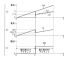
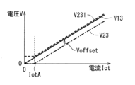
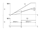
- FIG. 13A is a graph showing the relationship between each voltage and offset voltage Voffset for output current Iot in power supply device 58 of FIG. 12.
- FIG. 13B is a graph showing output currents Io1 and Io2 for output current Iot in power supply device 58 of FIG. 12 when there is an intentionally applied offset voltage Voffset.
- FIG. 13C is a graph showing output currents Io1 and Io2 for output current Iot in power supply device 58 of FIG. 12 when there is no intentionally applied offset voltage Voffset.
- an offset voltage source 30 is provided in the operational amplifier circuit 21, so that the converted voltage V23 is controlled to be lower than the converted voltage V13 as shown in FIG. 13A, and the output current Io2 of the current control unit 201G is cut off when there is no load.
- the transistor Q1 in the voltage control unit 101A flows an output current Iot1 equal to or greater than a certain level, and until the converted voltage V13 becomes larger than the offset voltage source 30, the voltage V231 on the non-inverting input terminal side of the operational amplifier circuit 21 becomes higher, so that the PMOS transistor Q12 and the output transistor Q11 are controlled to be turned off.
- the offset voltage source 30 prevents the current control unit 201G from starting unnecessarily when there is no load, and prevents the output voltage Vout from rising, even without providing a circuit to stop the operational amplifier circuit 21.
- the offset voltage source 30 corresponds to a component of a part of the start-up control circuit of the above-mentioned embodiments 1 to 7.
- Fig. 14 is a circuit diagram showing a configuration example of a power supply device 59 according to embodiment 9.
- the power supply device 59 according to embodiment 9 differs from the power supply device 58 according to embodiment 8 in Fig. 12 in the following points.
- a current control unit 201H is provided instead of the current control unit 201G.
- a bias voltage generating circuit 31 and a PMOS transistor Q19 are provided. The differences will be explained below.
- an input terminal P11 of a current control section 201H is connected to an input terminal of a current-voltage conversion circuit 23 via the source and drain of a PMOS transistor Q19, which is a bias transistor.
- a bias voltage generation circuit 31 generates a predetermined bias voltage Vbias and applies it to the gate of the PMOS transistor Q19.
- the PMOS transistor Q19 generates a current I19 corresponding to the bias voltage Vbias and causes it to flow into the current-voltage conversion circuit 23.
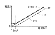
- FIG. 15 is a graph showing the relationship between the output current Iot and the current flowing into the current-voltage conversion circuits 13 and 23 in the power supply device 59 of FIG. 14.
- the current I2 detected by the current-voltage conversion circuit 13 (current detection circuit) of the voltage control unit 101A becomes smaller than the bias current I19 by the bias voltage generation circuit 31, and the converted voltage V23 becomes larger than the converted voltage V13, so that the PMOS transistor Q12 and the output transistor Q11 are controlled to be turned off.
- the bias voltage generating circuit 31 and the PMOS transistor Q19 are provided.
- the bias voltage generating circuit 31 causes the operational amplifier circuit 21 to recognize that the current control unit 201H is passing a larger current than the voltage control unit 101A, and an offset is applied so that the current control unit 201H tends to reduce the output current Io2. Therefore, the power supply device 59 according to the ninth embodiment has the same effect as the power supply device 58 according to the eighth embodiment.
- FIG. 16 is a circuit diagram showing a configuration example of a power supply device 60 according to embodiment 10.
- the power supply device 60 according to embodiment 10 differs from the power supply device 59 according to embodiment 9 in Fig. 14 in the following points.
- a current control unit 201I is provided instead of the current control unit 201H.
- the current control unit 201I further includes a reference voltage generating circuit 32, a comparator 33, and a PMOS transistor Q20. The differences will be explained below.
- the input terminal P11 of the current control unit 201I is connected to the input terminal of the current-voltage conversion circuit 23 via the source and drain of the PMOS transistor Q19 and the source and drain of the PMOS transistor Q20.
- the converted voltage V13 input to the input terminal P15 is input to the non-inverting input terminal of the operational amplifier circuit 21 and the non-inverting input terminal of the comparator 33.
- the reference voltage generation circuit 32 outputs a predetermined reference voltage Vref6 to the inverting input terminal of the comparator 33.
- the comparator 33 applies an L-level current detection signal S33 to the gate of the PMOS transistor Q20 to turn on the PMOS transistor Q20, thereby allowing the offset current I19 to flow.
- the comparator 33 applies an H-level current detection signal S33 to the gate of the PMOS transistor Q20 to turn off the PMOS transistor Q20, thereby preventing the offset current I19 from flowing.
- NMOS transistor Q20, comparator 33, and reference voltage generating circuit 32 are an example of a switching control circuit.
- the current control unit 201I configured as described above is characterized in that the start-up control of the operational amplifier circuit 21 by the comparator 24 of the power supply device 53 in FIG. 5 is realized by the reference voltage of the operational amplifier circuit 21 by current control of the PMOS transistor Q20.
- FIG. 17 is a timing chart showing the current and voltage in the power supply device 60 of FIG. 16.
- the voltage detection signal S33 of the comparator 33 goes to L level, and by turning on the PMOS transistor Q20, an offset current I19 is added so that the output current Io2 of the current control unit 201I is smaller than the output current Io1 of the voltage control unit 101A.
- the offset current I19 of the current control unit 201I is not allowed to flow. This suppresses bias in the output current when the output current is equal to or higher than a certain threshold value.
- the output current Io2 of the current control unit 201I is reduced so that the output voltage Vout does not rise, and when a predetermined threshold output current begins to flow, the PMOS transistor Q20 is turned off, thereby adjusting the current balance of each control unit 101A, 201I, thereby preventing current imbalance during heavy load when the influence of heat generation is significant.
- the power supply device of the present invention can monitor the operating state of the master voltage control unit and, if necessary, control the slave current control unit to suppress the current output, thereby preventing the output voltage from rising to the input voltage.
- An electronic device may be configured with the power supply devices 51 to 60 according to the embodiments and the load 301.
- the electronic device may be, for example, an electronic device for an automobile that receives power supply, or an image forming device such as a copier or printer that receives power supply, a personal computer, a tablet, a smartphone, a mobile phone, etc.
Landscapes
- Engineering & Computer Science (AREA)
- Physics & Mathematics (AREA)
- Electromagnetism (AREA)
- General Physics & Mathematics (AREA)
- Radar, Positioning & Navigation (AREA)
- Automation & Control Theory (AREA)
- Continuous-Control Power Sources That Use Transistors (AREA)
Abstract
無負荷時等に出力電圧が上昇することを防止可能な電源装置を提供する。電源装置は、互いに並列に接続された電圧制御部と電流制御部とを備える。電圧制御部は、入力電圧に基づいて、所定の基準電圧を発生する基準電圧回路と、電圧制御部の出力電圧が実質的に基準電圧に対応する電圧になるように電圧制御部の出力電流を制御することで、入力電圧に基づいて電圧制御部の出力電圧を発生して出力する電圧制御回路とを備える。電流制御部は、電流制御部の出力電流を検出して当該出力電流に対応する値を示す電流検出信号を発生して出力する電流検出回路と、電流検出信号が実質的に、電圧制御部の出力電流値に対応する値になるように電流制御部の出力電流を制御する電流制御回路と、電圧制御部の出力電流が所定のしきい値以上となったときに電流制御回路を起動して電流制御部の出力電流を流すように制御する起動制御回路とを備える。
Description
本発明は、例えば、基準電圧発生回路を用いたリニアレギュレータである電圧制御部と、少なくとも1個の電流制御部とを備える電源装置と、前記電源装置を備える電子機器とに関する。
従来技術に係る電源装置において、例えばリニアレギュレータを使用した場合に、入力電圧と出力電圧の差と、出力電流に応じて発熱する。その発熱は基板及びモールドによって許容量が決定される。すなわち、リニアレギュレータの出力電流に制限があり、要求する負荷電流値を満たさない場合がある。
その対応策として、複数個のリニアレギュレータを並列に接続し、各リニアレギュレータの出力端子を負荷に共通接続しようと考えると、製造プロセスのバラつきなどの影響により、各々異なった出力設定電圧を持つ複数のリニアレギュレータが存在することになる。そのため、出力設定電圧が一番高いリニアレギュレータから出力電流が供給される一方、出力設定電圧が低いリニアレギュレータでは、自身の出力設定電圧よりも高く出力電圧が固定されるため、内部回路が出力電流を止めるよう働きかける。
負荷電流が増大すると出力電圧が低下し始めるため、ある一定以上の負荷電流のもとでは、出力設定電圧が低いリニアレギュレータの出力設定電圧を下回ると、こちらのレギュレータから出力電流の供給が開始される。しかし、出力電流の供給バランスは不均一であり、出力設定電圧が低いリニアレギュレータが他方のリニアレギュレータの出力電流と同等に出力電流を供給できないため、要求する負荷電流値を満たせなくなる可能性がある。また、信頼性の面において、出力電流に不均衡が生じると発熱にも不均衡が生じるため、出力電流が一番多いリニアレギュレータの寿命を加速させ、破壊につながる恐れがある。
上記の電源回路において、2つのリニアレギュレータの入力端子と出力端子を共通にして並列接続すると、出力電流の供給が不均一になってしまう。ここで、各々のリニアレギュレータが自身の出力電流を検知し、それをアナログ電圧信号に変換して各々のバス端子を介して、一方のリニアレギュレータから電圧信号情報を出力し、他方のリニアレギュレータへ電圧信号情報を入力して各々の電圧信号を比較することで、2つのリニアレギュレータの出力電流を均等に保つ技術が既に知られている。
上記のような従来の電流を均等に保つ方式では、製造プロセスのバラつきなどの影響により、電流情報を入力されるスレーブ側が電流情報を出力するマスター側に比べて多く電流を流すようにオフセットが発生してしまうと、無負荷時にマスター側が電流を停止するように制御しようとするにも関わらず、スレーブ側が電流を流してしまい、出力電圧が入力電圧まで上昇してしまうという問題点があった。
本発明の目的は、上記問題点を解消し、無負荷時又は軽負荷時において、出力電圧が上昇することを防ぐことができる電源装置、及び前記電源装置を備える電子機器を提供することにある。
本開示の一態様に係る電源装置は、
電圧制御部と電流制御部とを備え、前記電圧制御部と前記各電流制御部とを互いに並列に接続して構成された電源装置であって、
前記電圧制御部は、
入力電圧に基づいて、所定の基準電圧を発生する基準電圧回路と、
前記電圧制御部の出力電圧が実質的に前記基準電圧に対応する電圧になるように前記電圧制御部の出力電流を制御することで、前記入力電圧に基づいて前記電圧制御部の出力電圧を発生して出力する電圧制御回路とを備え、
前記電流制御部は、
前記電流制御部の出力電流を検出して当該出力電流に対応する値を示す第1の電流検出信号を発生して出力する第1の電流検出回路と、
前記第1の電流検出信号が実質的に、前記電圧制御部の出力電流に対応する値になるように前記電流制御部の出力電流を制御する電流制御回路と、
前記電圧制御部の出力電流が所定の第1のしきい値以上となったとき、前記電流制御回路を起動して前記電流制御部の出力電流を流すように制御する起動制御回路とを備える。
従って、本開示の一態様に係る電源装置によれば、無負荷時又は軽負荷時において、出力電圧が入力電圧まで上昇することを防ぐことができ、出力電圧が上昇することを防ぐことができる。
以下、本発明に係る実施形態及び変形例について図面を参照して説明する。なお、同一又は同様の構成要素については同一の符号を付している。
(発明者の知見)
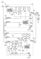
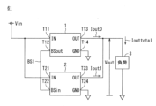
図18は特許文献1に開示された比較例に係る電源装置61の構成を示すブロック図である。
図18は特許文献1に開示された比較例に係る電源装置61の構成を示すブロック図である。
図18において、電源装置61は、電圧制御部1と、電流制御部2とを備えて構成される。ここで、電圧制御部1の入力端子T11と、電流制御部2の入力端子T21とは互いに接続されるとともに、入力電圧Vinの電圧源に接続される。また、電圧制御部1の出力端子T13と、電流制御部2の出力端子T23とは互いに接続されるとともに、負荷3に接続される。これにより、電圧制御部1と電流制御部2とは互いに並列に接続される。さらに、電圧制御部1の電流検出信号出力端子T12と、電流制御部2の電流検出信号入力端子T22とは互いに接続され、電圧制御部1の接地端子T14と、電流制御部2の接地端子T24は互いに接続されて接地される。なお、図18等において、INは入力電圧の入力端子を示し、OUTは出力端子を示し、BSoutは電流検出信号BS1の出力端子を示し、BSinは電流検出信号BSの入力端子を示し、GNDは接地端子を示す。
以上のように構成された電源装置61において、入力電圧Vinは、電圧制御部1の入力端子T11及び電流制御部2の入力端子T21に入力される。電圧制御部1は、基準電圧発生回路を内蔵するリニアレギュレータであって、入力電圧Vinを基準電圧になるように制御する。電圧制御部1からの出力電流Iout0と、電流制御部2からの出力電流Iout1を加算した合計電流Iouttotalが負荷3に流れる。
また、電圧制御部1は、出力電流Iout0に対して例えば比例するなど所定の相関を有して対応するアナログ電圧信号である電流検出信号BS1を発生して、電流検出信号出力端子T12から、電流制御部2の電流検出信号入力端子T22に出力する。これに応答して、電流制御部2は、出力電流Iout1に対して例えば比例するなど所定の相関を有して対応するアナログ電圧信号である電流検出信号を発生して、当該電流検出信号を入力される電流検出信号BS1と比較することにより、その差が実質的にゼロになるように制御し、すなわち、出力電流Iout0と出力電流Iout1が互いに、例えば等しくなるように、電流制御部2の出力電流Iout1を制御する出力トランジスタ(例えば図1のMOSトランジスタQ11に対応する)のインピーダンスが制御される。
負荷3は、電圧制御部1及び電流制御部2から電源電圧及び電源電流の供給を受ける、所定の機能を有する例えば電子機器であり、具体的には、電源供給を受ける自動車用の電子機器、もしくは、電源供給を受けるコピー機又はプリンタといった画像形成装置、パーソナルコンピュータ、タブレット、スマートホン、携帯電話機等である。
以上のように構成された電源装置61によれば、電圧制御部1における電圧制御系と、電流制御部2における電流制御系とは分離されているので、互いに影響を及ぼすことがない。従って、従来技術に比較して安定な制御系を確立して、不要な発振を防止することができる電源装置61を実現できる。
しかしながら、上記のような比較例に係る電流を均等に保つ方式の電源装置61では、製造プロセスのバラつきなどの影響により、電流情報を入力されるスレーブ側の電流制御部2が電流情報を出力するマスター側の電圧制御部1に比べて、多く電流を流すようにオフセットが発生してしまうと、無負荷時にマスター側の電圧制御部1が電流を停止するように制御しようとするにも関わらず、スレーブ側の電流制御部2が電流を流してしまい、出力電圧Voutが入力電圧Vinまで上昇してしまうという問題点があった。
本発明に係る実施形態の目的は、上記問題点を解消し、無負荷時又は軽負荷時において、出力電圧が上昇することを防ぐことができる電源装置、及び前記電源装置を備える電子機器を提供することにあり、各実施形態について以下に説明する。
(実施形態1)
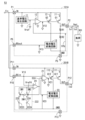
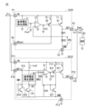
図1は実施形態1に係る電源装置51の構成例を示す回路図である。
図1は実施形態1に係る電源装置51の構成例を示す回路図である。
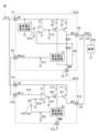
図1において、電源装置51は、電圧制御部101と、電流制御部201とを備えて構成される。ここで、電圧制御部101の入力端子P1(IN)と、電流制御部201の入力端子P2と(IN)は互いに接続されるとともに、入力電圧Vinの電圧源に接続される。また、電圧制御部101の出力端子P2(OUT)と、電流制御部201の出力端子P12(OUT)とは互いに接続されるとともに、負荷301に接続される。これにより、電圧制御部101と電流制御部201とは互いに並列に接続される。さらに、電圧制御部101の電流検出信号(電流I3)を出力する出力端子P4(BSmout)と、電流制御部102の電流検出信号(電流I3)を入力する入力端子P14(BSmin)とは互いに接続される。また、電圧制御部101の電流電圧変換信号(変換電圧V13)を出力する出力端子P5(BSout)と、電流制御部102の電流電圧変換信号(変換電圧V13)を入力する入力端子P15(BSin)とは互いに接続される。電圧制御部101の接地端子P3と、電流制御部201の接地端子P13は互いに接続されて接地される。
以上のように構成された電源装置51において、入力電圧Vinは、出力電圧Voutを決定する基準電圧リニアレギュレータを構成する電圧制御部101の入力端子P1に入力されるとともに、電流制御部201の入力端子P11に入力される。電圧制御部101の出力端子P2からの出力電流Io1と、電流制御部201の出力端子P12からの出力電流Io2とは加算された後、加算電流Iotが負荷301に流れる。電圧制御部101において検出されるアナログ電流検出信号であって、出力電流Io1と相関を有し、例えば比例関係で対応するアナログ電流検出信号(電流I3)は、出力端子P4及び電流制御部201の入力端子P14を介して電流制御部201に入力される。電流制御部201は、電流制御部201の出力電流Io2と相関を有し、例えば比例関係で対応する電流電圧変換信号(変換電圧V23)を発生し、電圧制御部101の電流電圧変換信号(変換電圧V13)を電流制御部201の電流電圧変換信号(変換電圧V23)と比較することで、出力電流Io1と出力電流Io2とが互いに等しくなるように電流制御部201の出力トランジスタQ11のインピーダンスが制御される。なお、電流電圧変換信号は電流検出信号の一例であり、以下の明細書において同様である。
電圧制御部101は基準電圧リニアレギュレータであって、基準電圧発生回路11と、演算増幅回路12と、電流電圧変換回路13と、PMOSトランジスタQ1~Q3と、分圧抵抗R1,R2とを備えて構成される。基準電圧発生回路11は入力電圧Vinに基づいて所定の基準電圧Vrefを発生して演算増幅回路12の反転入力端子に出力する。演算増幅回路12は、分圧抵抗R1,R2により分圧された帰還電圧Vfbから基準電圧Vrefを減算して増幅した誤差電圧V12をPMOSトランジスタQ1~Q3の各ゲートに出力する。
PMOSトランジスタQ1は、誤差電圧V12に基づいて、入力電圧Vinから発生した出力電流I1を制御して、出力電流Io1を発生して出力端子P2から負荷301に出力する。PMOSトランジスタQ2は、入力電圧Vinから、出力電流Io1と相関を有し例えば比例関係で対応する検出電流I2(=a・I1(a>0))を発生して電流電圧変換回路13に出力する。電流電圧変換回路13は、検出電流I2をそれに対応し、例えば比例する検出電圧に変換して電流電圧変換信号(変換電圧V13)として出力端子P5を介して電流制御部201の入力端子P15に出力する。PMOSトランジスタQ3は、入力電圧Vinから、出力電流Io1と相関を有し例えば比例関係で対応する検出電流I3(=b・I1(b>0))を発生して出力端子P4を介して電流制御部201の入力端子P14に出力する。分圧抵抗R1,R2は、出力電流Io1で発生される出力電圧Voutを帰還電圧Vfbに分圧して演算増幅回路12の非反転入力端子に出力する。
以上のように構成された電圧制御部101では、演算増幅回路12と、PMOSトランジスタQ1と、分圧抵抗R1,R2とにより構成される帰還制御回路(電圧制御回路)が、分圧電圧Vfbが基準電圧Vrefになるように出力トランジスタであるPMOSトランジスタQ1の出力電流I1を制御する。
電流制御部201は、演算増幅回路21と、電流検出回路22と、電流電圧変換回路23と、PMOSトランジスタQ11,Q12とを備えて構成される。演算増幅回路21は、電流電圧変換回路23からの電流電圧変換信号(変換電圧V23)から電流電圧変換信号(変換電圧V13)を減算して増幅した誤差電圧V21を、PMOSトランジスタQ11,Q12の各ゲートに出力する。PMOSトランジスタQ11は、誤差電圧V21に基づいて、入力電圧Vinから発生した出力電流I11を制御して、出力電流Io2を発生して出力端子P12から負荷301に出力する。PMOSトランジスタQ12は、入力電圧Vinから、出力電流Io2と相関を有し例えば比例関係で対応する検出電流I12(=c・I11(c>0))を発生して電流電圧変換回路23に出力する。
電流電圧変換回路23は、検出電流I12を、それに対応し例えば比例する検出電圧に変換して電流電圧変換信号(変換電圧V23)として演算増幅回路21の非反転入力端子に出力する。電流検出回路22は入力端子P14に入力される電流I3に基づいて、電流I3が所定の第3のしきい値電流未満のとき、Lレベルの電流検出信号S22を発生して演算増幅回路21の起動制御端子に非起動信号として出力する一方、電流I3が第3のしきい値電流以上のとき(すなわち、出力電流I1が所定の第1のしきい値電流以上のとき)、Hレベルの電流検出信号S22を発生して演算増幅回路21の起動制御端子に起動信号として出力することで、演算増幅回路21を含む電流制御回路を起動して電流制御部の出力電流を流すように制御する。ここで、演算増幅回路21はHレベルの電圧検出信号に応答して起動して演算増幅処理を実行するが、Lレベルの電圧検出信号に応答して起動しない。
ここで、電流検出回路22は起動制御回路の一例である。なお、起動信号と非起動信号とを総称して、起動制御信号という。当該起動制御信号は、起動制御回路が発生する信号である。
以上のように構成された電流制御部201では、電流I3に対応する出力電流I1が所定の第1のしきい値電流以上のとき、電流検出回路22と、PMOSトランジスタQ12と、電流電圧変換回路23とにより構成される帰還制御回路(電流制御回路)が、出力電流Io1と出力電流Io2とが互いに等しくなるように出力トランジスタであるPMOSトランジスタQ11の出力電流I11を制御する。一方、電流検出回路22に所定の第3のしきい値電流以上の電流が流入していないときは、演算増幅回路21の動作を停止し、演算増幅回路21の出力端子に接続される出力トランジスタであるPMOSトランジスタQ11の動作を停止するように制御することで、電流制御部201の出力電流Io2が発生しない。
以上のように構成された電源装置51において、一般的には、電圧制御部101からの出力電流Io1と、電流制御部201からの出力電流Io2とが互いに実質的に同じになるように設定される。しかし、例えば、製造バラつきによって、演算増幅回路21にオフセット電圧Voffが付加された場合(以下、第1のケースという。)、もしくは、電流制御部201内の帰還制御回路の所定の利得によるシステマティックオフセット電圧が発生した場合(以下、第2のケースという。)、出力電流Io1,Io2が互いに実質的に同一でなくなる。
前者の第1のケースの例では、電流電圧変換回路13,23の入力抵抗をRin[Ω]とすることを想定し、電流I1と電流I2のカレントミラー比をA1:A2(A2/A1=a)と仮定すると、演算増幅回路21で発生したオフセット電圧Voffに対し、出力トランジスタQ1,Q11の出力電流差ΔIは次式で表される。
ΔI=Voff×A1/(A2×Rin) (1)
このとき、出力トランジスタQ1の出力電流I1に比べて出力トランジスタQ11の出力電流I11が多くなるようにオフセット電圧Voffが発生していた場合に、出力端子P2,P12に負荷3が接続されていない無負荷状態であるときを考える。このとき、電圧制御部101が出力電流Io1の出力を停止して出力電圧Voutを所定値に保持しようとするにも関わらず、電流制御部201が所定の出力電流Io2を流してしまい、出力端子P2,P12の出力電圧Voutが入力端子P1,P11の入力電圧Vinまで上昇してしまう。後者の第2のケースの例においても、システマティックオフセット電圧により電流制御部201が所定の出力電流Io2を流してしまう場合には、出力端子P2,P12の出力電圧Voutが入力端子P1,P11の入力電圧Vinまで上昇してしまう。そのため、上記の電流差程度もしくは前記第1のしきい値電流以上の出力電流Io1が流れ始めるまで、電流制御部201が電流を流さないように制御することで、上記課題を解決する。
以上説明したように、実施形態1によれば、電流制御部201において、電流検出回路22を設け、電流検出回路22が電流I1に対応する出力電流I3が第3のしきい値電流未満のときに演算増幅回路21を起動しないように制御するので、演算増幅回路21にオフセット電圧Voffが付加された場合であっても、出力電圧Voutが上昇することを防ぐことができる。
従って、実施形態1に係る電源装置51によれば、マスター側の電圧制御部101の駆動状態を監視し、必要に応じてスレーブ側の電流制御部201の電流出力を抑制するように制御できることから、出力電圧Voutが入力電圧Vinまで上昇することを防ぐことができる。すなわち、無負荷時又は軽負荷時にはスレーブ側の電流制御部201の出力電流Io2の出力を停止することで出力電圧Voutが上昇することを防ぐことができる。
なお、実施形態1では、電圧制御部1の出力電流Io1と、電流制御部2の出力電流Io2が互いに実質的に等しくなるように、電流制御部2の出力電流Io2を制御している。しかし、電圧制御部1の出力電流Io1と、電流制御部2の出力電流Io2との比の値が所定値になるように、電流制御部2の出力電流Io2を電流分散して制御してもよい。
(実施形態1の変形例)
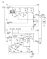
図2は実施形態1の変形例に係る電源装置51Aの詳細構成例を示す回路図であり、図2において、電流検出回路22の詳細構成例を示す。なお、以下では、図1との相違点について説明する。
図2は実施形態1の変形例に係る電源装置51Aの詳細構成例を示す回路図であり、図2において、電流検出回路22の詳細構成例を示す。なお、以下では、図1との相違点について説明する。
図2において、電流検出回路22は、ダイオード接続のNMOSトランジスタQ13と、コンパレータ221と、基準電圧発生回路222とを備えて構成される。ここで、基準電圧発生回路222は、2個のスイッチSW1,SW2と、それぞれ電圧V223=A3×Idet,V224=A3×Idet/2を有する2個の電圧源223,224と、インバータINV1とを備えて構成される。ここで、A3は電流電圧変換係数である。
入力端子P14に入力される電流I3は、NMOSトランジスタQ13のドレイン及びソースを介して接地されて対応する電圧V3に変換された後、変換された電圧V3がコンパレータ221の非反転入力端子に印加される。コンパレータ221は、変換された電圧V3を、基準電圧発生回路222からの基準電圧Vref2と比較して、V3<Vref2のとき、Lレベルの電流検出信号S22を発生して演算増幅回路21の起動制御端子に非起動信号として出力する一方、V3≧Vref2のとき、Hレベルの電流検出信号S22を発生して演算増幅回路21の起動制御端子に起動信号として出力する。コンパレータ221からの電流検出信号S22はスイッチSW2の制御端子に入力されるとともに、インバータINV1を介してスイッチSW1の制御端子に入力される。スイッチSW1,SW2はそれぞれ、制御端子にHレベルの制御信号が入力されるときにオンされる一方、Lレベルの制御信号が入力されるときにオフされる。
ここで、コンパレータ221と基準電圧発生回路222は切替制御回路の一例である。
以上のように構成された電流制御部201において、モニタトランジスタであるPMOSトランジスタQ3の電流I3が増大するにつれて、ダイオード接続されたNMOSトランジスタQ13のドレイン電圧V3が上昇するため、その電圧V3の上昇を検知するために、コンパレータ221は、当該電圧V3を、基準電圧発生回路222の基準電圧Vref2と比較することで電流検出信号S22を発生する。
以上の図2の電流制御部201の電流検出回路22において、NMOSトランジスタQ13に代えて、抵抗と、バイアス電流源の直列回路で構成してもよい。
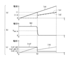
図3は図2の電源装置51Aの動作を示す各電流及び電圧のタイミングチャートである。図3を参照して、図2の電源装置51Aの動作について以下に説明する。
図3の時刻t1で、電流制御部201が起動すると、全体の出力電流Iotの半分を電流制御部201が分担するため(図3(a)参照)、電流電圧変換回路13からの変換電圧V13が低下する。このとき、出力トランジスタQ1,Q11の各電流Io1,Io2はおおよそ互いに同一で、全体の出力電流Iotの半分程度に分流するため、モニタトランジスタQ3の電流I3はその最大値のおよそ半分程度となる(図3(b)参照)。このとき、電流制御部201をディスエーブルする、電流I3に対するしきい値電流をIrelは、電流制御部201の起動検出用しきい値電流Idetの半分以下ではないとき、電流制御部201は再度ディスエーブルしてしまう。そのため、チャタリングを防ぐために解除しきい値電流Irelは前記起動検出用しきい値電流Idetの半分以下になるように、ヒステリシス特性を設ける。また、このときに使用する電圧源223,224は、上記の条件に合うようにそれぞれ、例えば電圧V223=A3×Idet,V224=A3×Idet/2を有するように調整されることが好ましい。
以上説明したように、実施形態1の変形例によれば、図3(c)に示すように、コンパレータ221の電流検出信号S22を用いて、電圧源223,224を選択的に切り替えすることで、所定のヒステリシス特性を有して電流制御部201の起動又は停止を選択的に切り替えることができる。これにより、電流制御部201が起動後、意図しない解除を防止することで、起動と停止を繰り返すことによるチャタリングなどの発振を防止することができる。
(実施形態2)
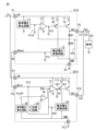
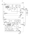
図4は実施形態2に係る電源装置52の構成例を示す回路図である。図4において、実施形態2に係る電源装置52は、図1の電源装置51に比較して以下の点が異なる。
(1)電流制御部201に代えて、電流制御部201Aを備える。
(2)電流制御部201Aにおいて、電流検出回路22に代えて、電流検出回路22Aを備える。電流検出回路22Aは、モニタトランジスタであるダイオード接続のNMOSトランジスタQ14と、コンパレータ221と、基準電圧発生回路225とを備える。ここで、基準電圧発生回路225は所定の基準電圧Vref3を発生してコンパレータ221の反転入力端子に出力する。
(3)電流制御部201Aにおいて、モニタトランジスタであるPMOSトランジスタQ13をさらに備える。PMOSトランジスタQ13のソースは入力端子P11に接続され、そのゲートは演算増幅回路21の出力端子に接続される。PMOSトランジスタQ13は、出力電流I11と相関関係を有してそれに対応して例えば比例する電流I13(=d・I11(d>0))を発生してNMOSトランジスタQ14のドレイン及びゲートに流入させる。
以下、相違点について説明する。
図4の電流制御部201Aは、電流検出回路22Aの検出対象を、電流I3に加えて、電流制御部201Aの出力電流I11に対応する電流I13を加算した電流値とし、NMOSトランジスタQ14は当該電流値を電圧に変換してコンパレータ221の非反転入力端子に印加する。
ここで、電流検出回路22Aは起動制御回路の一例である。
以上のように構成された電源装置52において、電流制御部201Aが起動されると、電圧制御部101の出力電流Io1の半分について、電流制御部201がその発生を分担するために、図1のモニタトランジスタQ3検出電流が減るが、電圧制御部101の出力電流Io1と電流制御部201の出力電流Io2の和は変わらないため、モニタトランジスタQ14の検出電流値は電流制御部201Aが起動する前のモニタトランジスタQ3の検出電流値と変わらない。従って、実施形態2に係る電源装置52は電源装置51と同様の作用効果を有し、電流制御部201Aの起動に伴う検出情報の変動をトリガとした発振現象を抑制できる。
(実施形態3)
図5は実施形態3に係る電源装置53の構成例を示す回路図である。図5において、実施形態3に係る電源装置53は、図2の電源装置51Aに比較して以下の点が異なる。
(1)電圧制御部101に代えて、PMOSトランジスタQ3及び出力端子P4を削除した電圧制御部101Aを備える。
(2)電流制御部201に代えて、入力端子P14を削除した電流制御部201Bを備える。電流制御部201Bはさらに、電流検出回路22に代えて、基準電圧発生回路222及びコンパレータ24を備える。
以下、相違点について説明する。
図5は実施形態3に係る電源装置53の構成例を示す回路図である。図5において、実施形態3に係る電源装置53は、図2の電源装置51Aに比較して以下の点が異なる。
(1)電圧制御部101に代えて、PMOSトランジスタQ3及び出力端子P4を削除した電圧制御部101Aを備える。
(2)電流制御部201に代えて、入力端子P14を削除した電流制御部201Bを備える。電流制御部201Bはさらに、電流検出回路22に代えて、基準電圧発生回路222及びコンパレータ24を備える。
以下、相違点について説明する。
図5において、電流電圧変換回路13から入力端子P15に入力される変換電圧V13は、演算増幅回路21の反転入力端子及びコンパレータ24の非反転入力端子に印加される。基準電圧発生回路222は、図2と同様に構成され、コンパレータ24は電流検出信号S24(コンパレータ24は入力される2つの電圧を比較しているので、電圧検出信号であるが、元々は、電流制御部101Aの出力電流に対応する電流検出信号なので、「電流検出信号」とし、以下同様である。)を演算増幅回路21の起動制御端子に出力するとともに、基準電圧発生回路222内のスイッチSW2の制御端子に入力され、また、インバータINV1を介してスイッチSW1の制御端子に入力される。なお、スイッチSW1,SW2はそれぞれ、制御端子にHレベルの制御信号が入力されるときにオンされる一方、Lレベルの制御信号が入力されるときにオフされる。
ここで、コンパレータ24は起動制御回路の一例であり、コンパレータ24と基準電圧発生回路222は切替制御回路の一例である。
以上のように構成された電源装置53は、電流電圧変換回路13からの変換電圧V13に基づいて、電流制御部201Bの起動判定を行うことを特徴としている。具体的には以下の通りである。コンパレータ24は、変換電圧V13を、基準電圧発生回路222からの基準電圧Vref4と比較して、V13<Vref4のとき、Lレベルの電流検出信号S24を発生して演算増幅回路21の起動制御端子に非起動信号として出力する一方、V13≧Vref4のとき、Hレベルの電流検出信号S24を発生して演算増幅回路21の起動制御端子に起動信号として出力する。
以上のように構成された電流制御部201Bにおいて、コンパレータ24は、変換電圧V13を、基準電圧発生回路222の基準電圧Vref4と比較することで電流検出信号S24を発生する。実施形態2と同様に、基準電圧Vref4を、ヒステリシス特性を有して選択的に切り替えることで電流制御部201Bのイネーブルとディスエーブルを繰り返すチャタリングを防止する。このとき、解除電流を検出電圧に対応する検出電流の半分以下とする必要があり、変換電圧V13が所定の基準電圧Vref4になったか否か、所定の解除電圧に対応する解除電流になったときの変換電圧V13を参照して電圧源223,224の電圧値V223,V224を設定する。
以上説明したように、実施形態3によれば、実施形態2と同様の作用効果を有する。
(実施形態4)
図6は実施形態4に係る電源装置54の構成例を示す回路図である。図6において、実施形態4に係る電源装置54は図5の電源装置53に比較して以下の点が異なる。
(1)電流制御部201Bに代えて、電流制御部201Cを備える。
(2)電流制御部201Cにおいて、基準電圧発生回路222に代えて、加算回路25及び基準電圧発生回路26を備える。
以下、相違点について説明する。
図6は実施形態4に係る電源装置54の構成例を示す回路図である。図6において、実施形態4に係る電源装置54は図5の電源装置53に比較して以下の点が異なる。
(1)電流制御部201Bに代えて、電流制御部201Cを備える。
(2)電流制御部201Cにおいて、基準電圧発生回路222に代えて、加算回路25及び基準電圧発生回路26を備える。
以下、相違点について説明する。
図6において、入力端子P15に入力される変換電圧V13は、演算増幅回路21の反転入力端子及び加算回路25の第1の入力端子に入力される。加算回路25の第2の入力端子には、電流電圧変換回路23からの変換電圧V23が入力され、加算回路25は、2つの入力端子に入力される電圧を加算して、加算結果の電圧(V13+V23)をコンパレータ24の非反転入力端子に出力する。基準電圧発生回路26は電流制御部201Cを起動又は解除する所定の基準電圧Vref5を発生してコンパレータ24の反転入力端子に出力する。コンパレータ24は、加算電圧(V13+V23)を基準電圧Vref5と比較して、(V13+V23)<Vref5のとき、Lレベルの電流検出信号S24を発生して演算増幅回路21の起動制御端子に非起動信号として出力する一方、(V13+V23)≧Vref5のとき、Hレベルの電流検出信号S24を発生して演算増幅回路21の起動制御端子に起動信号として出力する。
以上のように構成された電源装置54では、電流制御部201Cの起動判定に用いる検出対象電圧を、電流電圧変換回路13,23の変換電圧の和(V13+V23)としている。電流制御部201Cが起動すると、電圧制御部101Aの出力電流Io1の半分を、電流制御部201Cが分担するため、電流電圧変換回路13の変換電圧V13が低下する。しかし、電圧制御部101Aと電流制御部201Cの出力電流の和Iot(=Io1+Io2)は変わらないため、電流電圧変換回路13,23が出力する電圧制御部101A及び電流制御部201Cの電流情報の和は変わらない。
以上説明したように、実施形態4によれば、電流制御部201Cが起動後も電流検出情報が大きく変動しないことにより、電流制御部201Cの起動に伴う電流検出情報の変動に基づいて演算増幅回路21を起動する。これにより、電流制御部201Cが起動後、意図しない解除を防止することで、起動と停止を繰り返すことによるチャタリングなどの発振を防止することができる。
(実施形態5)
図7は実施形態5に係る電源装置55の構成例を示す回路図である。図7において、実施形態5に係る電源装置55は、図1の電源装置51に比較して以下の点が異なる。
(1)電圧制御部101に代えて、PMOSトランジスタQ3、出力端子P4、及び電流電圧変換回路13を削除した電圧制御部101Bを備える。
(2)電流制御部201に代えて、電流制御部201Dを備える。ここで、電流制御部201の電流検出回路22及び電流電圧変換回路23に代えて、基準電流発生回路28、カレントミラー回路CM1と、インバータINV2と、ダイオード接続のNMOSトランジスタQ17とを備える。
以下、相違点について説明する。
図7は実施形態5に係る電源装置55の構成例を示す回路図である。図7において、実施形態5に係る電源装置55は、図1の電源装置51に比較して以下の点が異なる。
(1)電圧制御部101に代えて、PMOSトランジスタQ3、出力端子P4、及び電流電圧変換回路13を削除した電圧制御部101Bを備える。
(2)電流制御部201に代えて、電流制御部201Dを備える。ここで、電流制御部201の電流検出回路22及び電流電圧変換回路23に代えて、基準電流発生回路28、カレントミラー回路CM1と、インバータINV2と、ダイオード接続のNMOSトランジスタQ17とを備える。
以下、相違点について説明する。
図7の電圧制御部101Bにおいて、PMOSトランジスタQ2に流れる電流I2は出力端子P5を介して電流制御部201Dの入力端子P15に入力される。
また、電流制御部201Dにおいて、カレントミラー回路CM1は、NMOSトランジスタQ15,Q16を備えて構成される。ここで、入力端子P15は、ダイオード接続されたNMOSトランジスタQ15のドレイン及びソースを介して接地され、NMOSトランジスタQ15のゲートはNMOSトランジスタQ16のゲートに接続される。入力端子P15に入力される電流I2は、カレントミラー回路CM1のNMOSトランジスタQ15により電圧V13に変換された後、演算増幅回路21の反転入力端子に入力される。
基準電流発生回路28は入力端子P11に印加される入力電圧Vinに基づいて、所定の基準電流Irefを発生してNMOSトランジスタQ16のドレインに出力する。基準電流発生回路28の出力端子はNMOSトランジスタQ16のドレイン及びソースを介して接地される。基準電流発生回路28からの基準電流Irefがカレントミラー回路CM1のNMOSトランジスタQ16に流れ込むが、NMOSトランジスタQ15に流れる電流に対応する電流I16がNMOSトランジスタQ16から流出する。すなわち、NMOSトランジスタQ16に流れる電流値はIref-I16となり、電流値(Iref-I16)に対応する電圧V91がNMOSトランジスタQ16のドレインに発生し、電圧V91はインバータINV2を介して起動信号である電圧検出信号S93として演算増幅回路21の起動制御端子に入力される。
さらに、PMOSトランジスタQ12のドレインは、ダイオード接続されたNMOSトランジスタQ17のドレイン及びソースを介して接地される。ここで、NMOSトランジスタQ17のドレイン及びゲートは演算増幅回路21の非反転入力端子に接続される。
ここで、インバータINV2と基準電流発生回路28とカレントミラー回路CM1は、起動制御回路の一例である。
以上のように構成された電源装置55において、電圧制御部101Bの出力電流Io1が増大して出力電流Io1に対応するI16が増大すると、電流値(Iref-I16)に対応する電圧V91がインバータINV2のしきい値VINV_TH未満となり、インバータINV2の電圧検出信号はLレベルからHレベルになる。従って、インバータINV2の起動制御信号がHレベルの起動信号となって演算増幅回路21を起動させる。
以上説明したように、実施形態5によれば、カレントミラー回路CM1によって電圧制御部101Bの出力電流Io1に対応する電流I2の情報を、電流制御部201Dにおけるカレントミラー回路CM1の電流I16にコピーすることで、電圧制御部101Bの出力電流Io1に比例した電流I16を基準電流Irefと比較し、比較結果信号を演算増幅回路21の起動制御信号として用いている。
実施形態5では、実施形態1~4に係る抵抗を用いた電流電圧変換回路13,23を用いることなく、ダイオード接続のNMOSトランジスタQ15を含むカレントミラー回路CM1及びダイオード接続のNMOSトランジスタQ17を用いる。これにより、別途定電圧発生回路又はコンパレータ等を用意する必要なく、極めて簡単に電流制御部201Dの演算増幅回路21の起動制御信号の判定回路を生成できる。
(実施形態6)
図8は実施形態6に係る電源装置56の構成例を示す回路図である。また、図9は図8の電源装置56の動作を示す各電流及び電圧のタイミングチャートである。図8において、電源装置56は、図7の電源装置55に比較して以下の点が異なる。
(1)電流制御部201Dに代えて、電流制御部201Eを備える。
(2)電流制御部201Eにおいて、基準電流発生回路28に代えて、基準電流発生回路28Aを備える。
(3)基準電流発生回路28Aは、定電流I29a,I29b(I29a+129b>I29a)をそれぞれ有する定電流源29a,29bと、スイッチトランジスタであるPMOSトランジスタQ29とを備える。図8において、基準電流発生回路28Aにおける各電流値は次式のように設定される。
Iref_det=I29a+129b(PMOSトランジスタQ29がオンのとき)
(2)
(2)
Iref_rel=I29a(PMOSトランジスタQ29がオフのとき)
(3)
(3)
ここで、図9(c)に示すように、
Iref_rel<Iref_det/2 (4)
である。
Iref_rel<Iref_det/2 (4)
である。
以下、相違点について説明する。
図8において、入力端子P11は定電流源29aを介してNMOSトランジスタQ16のドレインに接続されるとともに、定電流源29b及びPMOSトランジスタQ29のソース及びドレインを介してNMOSトランジスタQ16のドレインに接続される。インバータINV2からの電流検出信号S93はNMOSトランジスタQ29のゲートに印加される。PMOSトランジスタQ29は、Hレベルの電流検出信号S93に応答してオフされる一方、Lレベルの電流検出信号S93に応答してオンされる。
ここで、インバータINV2と、基準電流発生回路28Aと、カレントミラー回路CM1は起動制御回路の一例であり、インバータINV2と基準電流発生回路28Aは切替制御回路の一例である。
以上のように構成された電流制御部201Eでは、電流検出信号S93に応じて、基準電流Irefを電流I29a又は加算電流(I29a+I29b)のいずれかに選択的に切り替えることを特徴としている。
図7の実施形態5と同様に、電流制御部201Eが起動すると、全体の出力電流Iotの半分を電流制御部201Eが分担して生成するため(図9(a)参照)、電流I2に対応する電圧V13が低下し、カレントミラー回路CM1のNMOSトランジスタQ16に流れる電流I16が減少する。本来、出力トランジスタQ1の電流I1が所定のしきい値電流以上となったときに、図9(b)に示すように、時刻t2で、カレントミラー回路CM1はそれを検知して、NMOSトランジスタQ16のドレイン電圧V91はHレベルからLレベルになり、ドレイン電圧V91がインバータINV2のしきい値VINV_THを跨いだときに、演算増幅回路21のイネーブルを制御する起動制御信号S93はLレベルからHレベルとなる。
しかし、基準電流発生回路28Aの基準電流Irefがそのままであった場合、電圧制御部101Bの出力電流Io1に対応するカレントミラー回路CM1のNMOSトランジスタQ16の電流が減少する前記作用により、ドレイン電圧V91はLレベルからHレベルとなり、演算増幅回路21はディスエーブルされてしまい、上述のようにチャタリングが発生してしまう。そのため、基準電流発生回路28Aからの基準電流Irefを前記式(2)から前記式(3)に切り替え、電流I16に対する電圧V91の特性において、解除しきい値を下回らないようにヒステリシス特性を設ける。すなわち、チャタリングが発生しないようにするには、演算増幅回路21の電流検出信号S93がLレベルからHレベルとなったことを受けて、図9(c)に示すように、基準電流発生回路280の電流値Irefを半分以下の電流値Iref_relにすることが好ましい。
以上説明したように、実施形態6に係る電源装置56によれば、実施形態5と同様の作用効果を有し、さらに、電流制御部201Eが起動後、意図しない解除を防止することで、起動と停止を繰り返すことによる発振を防止することができる。
(実施形態7)
図10は実施形態7に係る電源装置57の構成例を示す回路図である。また、図11は図10の電源装置の動作を示す各電流及び電圧のタイミングチャートである。図10において、実施形態7に係る電源装置57は、図7の電源装置55に比較して以下の点が異なる。
(1)電流制御部201Dに代えて、電流制御部201Fを備える。
(2)電流制御部201Fにおいて、NMOSトランジスタQ18をさらに備え,NMOSトランジスタQ18とNMOSトランジスタQ17とにより、カレントミラー回路CM2を構成する。
以下、相違点について説明する。
図10は実施形態7に係る電源装置57の構成例を示す回路図である。また、図11は図10の電源装置の動作を示す各電流及び電圧のタイミングチャートである。図10において、実施形態7に係る電源装置57は、図7の電源装置55に比較して以下の点が異なる。
(1)電流制御部201Dに代えて、電流制御部201Fを備える。
(2)電流制御部201Fにおいて、NMOSトランジスタQ18をさらに備え,NMOSトランジスタQ18とNMOSトランジスタQ17とにより、カレントミラー回路CM2を構成する。
以下、相違点について説明する。
図10の電流制御部201Fにおいて、ダイオード接続されたNMOSトランジスタQ17と、NMOSトランジスタQ18の各ゲート及び各ソースは互いに接続されて、カレントミラー回路CM2を構成する。NMOSトランジスタQ18の電流I18は、電流制御部201Fの出力電流Io2=I11に比例するモニタ電流I12であって、モニタ電流I12に比例する電流となる。
図10の電流制御部201Fでは、図7の実施形態5とは異なり、電流制御部201Fの起動判定に用いる電流検出信号S93の検出対象電流を、カレントミラー回路CM1のNMOSトランジスタQ16の電流I16と、カレントミラー回路CM2のNMOSトランジスタQ18の電流I18との和電流としたことを特徴としている。
ここで、インバータINV2と、基準電流発生回路28と、カレントミラー回路CM1、CM2は起動制御回路の一例である。
図11の時刻t3で、電流制御部201Fが起動すると、全体出力電流Iotの半分を電流制御部201Fが分担するため、電流I16が減少するが、電圧制御部101Bと電流制御部201Fの各出力電流Io1,Io2の和電流Iotは変わらないため(図11(a)参照)、各制御部101B,201Fの出力電流の情報の和と相関性を持つカレントミラー回路CM1,CM2の和電流量は変わらない。
以上説明したように、実施形態7によれば、実施形態6と同様の作用効果を有し、電流制御部201Fが起動後も電流検出情報が大きく変動しないことにより、電流制御部201Fの起動に伴う電流検出情報の変動をトリガとした発振現象を抑制できる。
(実施形態8)
図12は実施形態8に係る電源装置58の構成例を示す回路図である。図12において、実施形態8に係る電源装置58は、図5の電源装置53に比較して以下の点が異なる。
(1)電流制御部201Bに代えて、電流制御部201Gを備える。電流制御部201Gは、電流制御部201Bに比較して、基準電圧発生回路222及びコンパレータ24に代えて、オフセット電圧V30を有するオフセット電圧源30を備える。なお、演算増幅回路21への起動制御信号である電流検出信号を用いない。
以下、相違点について説明する。
図12は実施形態8に係る電源装置58の構成例を示す回路図である。図12において、実施形態8に係る電源装置58は、図5の電源装置53に比較して以下の点が異なる。
(1)電流制御部201Bに代えて、電流制御部201Gを備える。電流制御部201Gは、電流制御部201Bに比較して、基準電圧発生回路222及びコンパレータ24に代えて、オフセット電圧V30を有するオフセット電圧源30を備える。なお、演算増幅回路21への起動制御信号である電流検出信号を用いない。
以下、相違点について説明する。
図12の電流制御部201Gにおいては、意図的に電圧制御部101Aの出力電流Io1よりも電流制御部201の出力電流Io2が低くなるよう、演算増幅回路21の非反転入力端子にオフセット電圧源30を設ける。すなわち、演算増幅回路21の非反転入力端子には、電流電圧変換回路23からの変換電圧V23と、オフセット電圧Voffsetとの和電圧が印加される。
図1の実施形態1にて説明したように、出力電圧Voutが入力端子T1の入力電圧Vinまで上昇してしまう現象は、電圧制御部101が出力電流Io1を止めて出力電圧Voutを保持しようとするにも関わらず、電流制御部201が出力電流Io2を流してしまうためである。電流制御部201が起動されたときに、演算増幅回路21が、その非反転入力端子の電圧よりも高い電圧に制御するようにオフセット電圧が付いてしまうことで、上記現象が顕在化する。
図13Aは図12の電源装置58において出力電流Iotに対する、各電圧とオフセット電圧Voffsetとの関係を示すグラフである。また、図13Bは図12の電源装置58において出力電流Iotに対する、意図的に付与したオフセット電圧Voffsetがあるときの出力電流Io1,Io2を示すグラフである。さらに、図13Cは図12の電源装置58において出力電流Iotに対する、意図的に付与したオフセット電圧Voffsetがないときの出力電流Io1,Io2を示すグラフである。
前記現象を回避するために、図12のように演算増幅回路21にオフセット電圧源30を設けることで、図13Aに示すように、変換電圧V23が変換電圧V13よりも低く制御し、無負荷時は電流制御部201Gの出力電流Io2をカットオフする。また、電圧制御部101A内のトランジスタQ1がある一定以上の出力電流Iot1を流し、変換電圧V13がオフセット電圧源30より大きくなるまで、演算増幅回路21の非反転入力端子側の電圧V231の方が高くなるため、PMOSトランジスタQ12及び出力トランジスタQ11をオフするよう制御する。図13B及び図13Cに示すように、前記オフセット電圧源30により、演算増幅回路21を停止する回路を設けずとも、無負荷時において電流制御部201Gが無用に起動せず、出力電圧Voutの浮き上がりを防止できる。すなわち、オフセット電圧源30が、上述した実施形態1~7の起動制御回路の一部の構成要素に相当する。
(実施形態9)
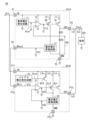
図14は実施形態9に係る電源装置59の構成例を示す回路図である。図14において、実施形態9に係る電源装置59は、図12の実施形態8に係る電源装置58に比較して以下の点が異なる。
(1)電流制御部201Gに代えて、電流制御部201Hを備える。
(2)電流制御部201Hにおいて、オフセット電圧源30に代えて、バイアス電圧発生回路31及びPMOSトランジスタQ19を備える。
以下、相違点について説明する。
図14は実施形態9に係る電源装置59の構成例を示す回路図である。図14において、実施形態9に係る電源装置59は、図12の実施形態8に係る電源装置58に比較して以下の点が異なる。
(1)電流制御部201Gに代えて、電流制御部201Hを備える。
(2)電流制御部201Hにおいて、オフセット電圧源30に代えて、バイアス電圧発生回路31及びPMOSトランジスタQ19を備える。
以下、相違点について説明する。
図14において、電流制御部201Hの入力端子P11はバイアストランジスタであるPMOSトランジスタQ19のソース及びドレインを介して電流電圧変換回路23の入力端子に接続される。バイアス電圧発生回路31は所定のバイアス電圧Vbiasを発生してPMOSトランジスタQ19のゲートに印加する。PMOSトランジスタQ19はバイアス電圧Vbiasに対応する電流I19を発生して、電流電圧変換
回路23に流入させる。すなわち、電流電圧変換回路23に流入する電流は、電流I12と電流I19の和となり、電流電圧変換回路23は和の電流(I12+I19)に対応する変換電圧V23を発生して演算増幅回路21の非反転入力端子に印加する。
回路23に流入させる。すなわち、電流電圧変換回路23に流入する電流は、電流I12と電流I19の和となり、電流電圧変換回路23は和の電流(I12+I19)に対応する変換電圧V23を発生して演算増幅回路21の非反転入力端子に印加する。
図15は図14の電源装置59において出力電流Iotに対する、電流電圧変換回路13,23に流れ込む電流の関係を示すグラフである。
以上のように構成された電源装置59では、図15と図14とを参照すると、図中、図15のIotAよりもIotが少ない条件では、電圧制御部101Aの電流電圧変換回路13(電流検出回路)により検出される電流I2が、バイアス電圧発生回路31によるバイアス電流I19よりも小さくなり、変換電圧V23が変換電圧V13よりも大きくなるため、PMOSトランジスタQ12及び出力トランジスタQ11をオフとするよう制御する。
以上説明したように、実施形態9によれば、実施形態8と同様のオフセット電圧Voffsetを付加するために、バイアス電圧発生回路31及びPMOSトランジスタQ19を設けた。ここで、バイアス電圧発生回路31によって、電流制御部201Hが電圧制御部101Aに比較して多大な電流を流しているかのように演算増幅回路21が認識し、電流制御部201Hが出力電流Io2を少なくする方向となるようにオフセットをつける。従って、実施形態9に係る電源装置59は、実施形態8に係る電源装置58と同様の作用効果を有する。
(実施形態10)
図16は実施形態10に係る電源装置60の構成例を示す回路図である。図16において、実施形態10に係る電源装置60は、図14の実施形態9に係る電源装置59に比較して以下の点が異なる。
(1)電流制御部201Hに代えて、電流制御部201Iを備える。
(2)電流制御部201Iは、電流制御部201Hに比較して、基準電圧発生回路32と、コンパレータ33と、PMOSトランジスタQ20とをさらに備える。
以下、相違点について説明する。
図16は実施形態10に係る電源装置60の構成例を示す回路図である。図16において、実施形態10に係る電源装置60は、図14の実施形態9に係る電源装置59に比較して以下の点が異なる。
(1)電流制御部201Hに代えて、電流制御部201Iを備える。
(2)電流制御部201Iは、電流制御部201Hに比較して、基準電圧発生回路32と、コンパレータ33と、PMOSトランジスタQ20とをさらに備える。
以下、相違点について説明する。
図16において、電流制御部201Iの入力端子P11はPMOSトランジスタQ19のソース及びドレインと、PMOSトランジスタQ20のソース及びドレインを介して電流電圧変換回路23の入力端子に接続される。入力端子P15に入力される変換電圧V13は演算増幅回路21の非反転入力端子及びコンパレータ33の非反転入力端子に入力される。基準電圧発生回路32は所定の基準電圧Vref6をコンパレータ33の反転入力端子に出力する。コンパレータ33は、変換電圧V13<Vref6のときに、Lレベルの電流検出信号S33をPMOSトランジスタQ20のゲートに印加してPMOSトランジスタQ20をオンすることでオフセット電流I19を流す。一方、コンパレータ33は、変換電圧V13≧Vref6のときに、Hレベルの電流検出信号S33をPMOSトランジスタQ20のゲートに印加してPMOSトランジスタQ20をオフすることでオフセット電流I19を流さない。
ここで、NMOSトランジスタQ20と、コンパレータ33と、基準電圧発生回路32とは切替制御回路の一例である。
以上のように構成された電流制御部201Iでは、図5の電源装置53のコンパレータ24による演算増幅回路21の起動制御を、PMOSトランジスタQ20の電流制御による演算増幅回路21の基準電圧により実現することを特徴としている。
図17は図16の電源装置60に電流及び電圧を示すタイミングチャートである。
図17に示すように、出力電流Iotがある一定値以下である場合、コンパレータ33の電圧検出信号S33はLレベルとなり、PMOSトランジスタQ20をオンすることで、電圧制御部101Aの出力電流Io1に対して電流制御部201Iの出力電流Io2を小さくするようオフセット電流I19を付加する。電流制御部201Iの出力電流Io2がある程度流れ始めたタイミング(時刻t4)でPMOSトランジスタQ20をオフにすることで、電流制御部201Iのオフセット電流I19を流さない。これにより、所定のしきい値出力電流以上の時には出力電流の偏りを抑える。
以上説明したように、実施形態10によれば、軽負荷時には、出力電圧Voutが浮き上がらないよう電流制御部201Iの出力電流Io2を減少させ、所定のしきい値出力電流が流れ始めると、PMOSトランジスタQ20をオフすることで、各制御部101A,201Iの電流バランスを整えることで発熱の影響が大きい重負荷時の電流の偏りを防止することができる。
(変形例)
以上の実施形態に係る電源装置では、電圧制御回路に使用した場合を例にして示したが、これは一例であり、本発明はこれに限定するものではなく、演算増幅回路を使用したすべての制御回路に適用することができる。例えば、電流制御回路に適用してもよい。
以上の実施形態に係る電源装置では、電圧制御回路に使用した場合を例にして示したが、これは一例であり、本発明はこれに限定するものではなく、演算増幅回路を使用したすべての制御回路に適用することができる。例えば、電流制御回路に適用してもよい。
以上詳述したように、本発明に係る電源装置によれば、マスター側の電圧制御部の駆動状態を監視し、必要に応じてスレーブ側の電流制御部の電流出力を抑制するように制御できることから、出力電圧が入力電圧まで上昇することを防ぐことができる。
実施形態に係る電源装置51~60と、負荷301とを備えて、電子機器を構成してもよい。電子機器は例えば、電源供給を受ける自動車用の電子機器、もしくは、電源供給を受けるコピー機又はプリンタといった画像形成装置、パーソナルコンピュータ、タブレット、スマートホン、携帯電話機等である。
1,101,101A~101B 電圧制御部
2,201,201A~201I 電流制御部
3,301 負荷
11 基準電圧発生回路
12 演算増幅回路
13 電流電圧変換回路
21 演算増幅回路
22,22A 電流検出回路
23 電流電圧変換回路
24 コンパレータ
25 加算回路
26 基準電圧発生回路
28,28A,29 基準電流発生回路
29a,29b 定電流源
30 オフセット電圧源
31 バイアス電圧発生回路
32 基準電圧発生回路
33 コンパレータ
51~61,51A 電源装置
221 コンパレータ
222 基準電圧発生回路
223,224 電圧源
225 基準電圧発生回路
CM1,CM2 カレントミラー回路
INV1,INV2 インバータ
Q1~Q29 MOSトランジスタ
R1,R2 分圧抵抗
SW1,SW2 スイッチ
T11~T24,P1~P15 端子
Claims (10)
- 電圧制御部と電流制御部とを備え、前記電圧制御部と前記各電流制御部とを互いに並列に接続して構成された電源装置であって、
前記電圧制御部は、
入力電圧に基づいて、所定の基準電圧を発生する基準電圧回路と、
前記電圧制御部の出力電圧が実質的に前記基準電圧に対応する電圧になるように前記電圧制御部の出力電流を制御することで、前記入力電圧に基づいて前記電圧制御部の出力電圧を発生して出力する電圧制御回路とを備え、
前記電流制御部は、
前記電流制御部の出力電流を検出して当該出力電流に対応する値を示す第1の電流検出信号を発生して出力する第1の電流検出回路と、
前記第1の電流検出信号が実質的に、前記電圧制御部の出力電流に対応する値になるように前記電流制御部の出力電流を制御する電流制御回路と、
前記電圧制御部の出力電流が所定の第1のしきい値以上となったとき、前記電流制御回路を起動して前記電流制御部の出力電流を流すように制御する起動制御回路とを備える、
電源装置。 - 前記電圧制御部又は前記電流制御部は、
前記電圧制御部の出力電流を検出して当該出力電流に対応する値を示す第2の電流検出信号を発生して出力する第2の電流検出回路をさらに備え、
前記起動制御回路は、前記第2の電流検出信号が所定の第2のしきい値以上となったときに前記電流制御回路を起動するように制御する、
請求項1に記載の電源装置。 - 前記第2の電流検出信号の値が前記第2のしきい値以上となったときに、前記第2のしきい値を、所定の第1の値から、前記第1の値よりも小さい所定の第2の値に選択的に切り替える第1の切替制御回路をさらに備える、
請求項2に記載の電源装置。 - 前記起動制御回路は、前記第1の電流検出信号と前記第2の電流検出信号の加算値が所定の第3のしきい値以上となったときに前記電流制御回路を起動するように制御する、
請求項2に記載の電源装置。 - 前記起動制御回路は、前記第2の電流検出信号が、前記第1の電流検出信号と所定のオフセット値の加算値以上となったときに前記電流制御回路を起動するように制御する、
請求項2に記載の電源装置。 - 前記起動制御回路は、前記第2の電流検出信号が、前記第1の電流検出信号と所定のバイアス電流値の加算値以上となったときに前記電流制御回路を起動するように制御する、
請求項2に記載の電源装置。 - 前記起動制御回路は、前記バイアス電流値を、前記第2の電流検出信号の値が所定の第3のしきい値以上となったときにゼロに切り替える第2の切替制御回路をさらに備える、
請求項6に記載の電源装置。 - 請求項1又は2に記載の電源装置と、
電子機器の負荷とを備える、前記電子機器。 - 請求項3に記載の電源装置と、
電子機器の負荷とを備える、前記電子機器。 - 請求項4~7のうちのいずれか1つに記載の電源装置と、
電子機器の負荷とを備える、前記電子機器。
Priority Applications (1)
| Application Number | Priority Date | Filing Date | Title |
|---|---|---|---|
| PCT/JP2023/030164 WO2025041267A1 (ja) | 2023-08-22 | 2023-08-22 | 電源装置及び電子機器 |
Applications Claiming Priority (1)
| Application Number | Priority Date | Filing Date | Title |
|---|---|---|---|
| PCT/JP2023/030164 WO2025041267A1 (ja) | 2023-08-22 | 2023-08-22 | 電源装置及び電子機器 |
Publications (1)
| Publication Number | Publication Date |
|---|---|
| WO2025041267A1 true WO2025041267A1 (ja) | 2025-02-27 |
Family
ID=94731532
Family Applications (1)
| Application Number | Title | Priority Date | Filing Date |
|---|---|---|---|
| PCT/JP2023/030164 Pending WO2025041267A1 (ja) | 2023-08-22 | 2023-08-22 | 電源装置及び電子機器 |
Country Status (1)
| Country | Link |
|---|---|
| WO (1) | WO2025041267A1 (ja) |
Citations (5)
| Publication number | Priority date | Publication date | Assignee | Title |
|---|---|---|---|---|
| JP2002125371A (ja) * | 2000-10-16 | 2002-04-26 | Sharp Corp | 多出力電源装置及びそれを備えた電子機器 |
| JP2005176409A (ja) * | 2003-12-08 | 2005-06-30 | Matsushita Electric Ind Co Ltd | 直流電源装置 |
| JP2006133935A (ja) * | 2004-11-04 | 2006-05-25 | Rohm Co Ltd | 電源装置、及び携帯機器 |
| JP2015146699A (ja) * | 2014-02-04 | 2015-08-13 | 三菱電機株式会社 | 電源装置 |
| JP7170935B2 (ja) * | 2020-03-18 | 2022-11-14 | 日清紡マイクロデバイス株式会社 | 電源装置及び電子機器 |
-
2023
- 2023-08-22 WO PCT/JP2023/030164 patent/WO2025041267A1/ja active Pending
Patent Citations (5)
| Publication number | Priority date | Publication date | Assignee | Title |
|---|---|---|---|---|
| JP2002125371A (ja) * | 2000-10-16 | 2002-04-26 | Sharp Corp | 多出力電源装置及びそれを備えた電子機器 |
| JP2005176409A (ja) * | 2003-12-08 | 2005-06-30 | Matsushita Electric Ind Co Ltd | 直流電源装置 |
| JP2006133935A (ja) * | 2004-11-04 | 2006-05-25 | Rohm Co Ltd | 電源装置、及び携帯機器 |
| JP2015146699A (ja) * | 2014-02-04 | 2015-08-13 | 三菱電機株式会社 | 電源装置 |
| JP7170935B2 (ja) * | 2020-03-18 | 2022-11-14 | 日清紡マイクロデバイス株式会社 | 電源装置及び電子機器 |
Similar Documents
| Publication | Publication Date | Title |
|---|---|---|
| KR101136691B1 (ko) | 정전압 회로 | |
| JP5027189B2 (ja) | 電源レギュレータ | |
| US9141121B2 (en) | Voltage regulator | |
| US8169202B2 (en) | Low dropout regulators | |
| KR101004851B1 (ko) | 출력 제어 기능을 갖는 전력증폭기 시스템 | |
| US8729876B2 (en) | Voltage regulator and related voltage regulating method thereof | |
| US10250128B2 (en) | Type III switching converter error amplifier with fast transient response behavior | |
| EP1258982B1 (en) | Operational amplifier arrangement including a quiescent current control circuit | |
| US6771122B2 (en) | DC offset compensation circuit of closed loop operational amplifier and method of compensating for DC offset | |
| CN113141113B (zh) | 具有自适应补偿的开关转换器 | |
| US20190068055A1 (en) | Switching regulator | |
| JP7170935B2 (ja) | 電源装置及び電子機器 | |
| CN107508462A (zh) | 针对负载的切换控制器和方法 | |
| WO2025041267A1 (ja) | 電源装置及び電子機器 | |
| CN110677025A (zh) | 调压器的电流限制 | |
| CN113748393A (zh) | 恒压电路以及电子设备 | |
| CN113273069B (zh) | 利用内部模拟控制环路向负载供电的电源和方法 | |
| US20180212691A1 (en) | Semiconductor integrated circuit, semiconductor system, and electric source voltage control method | |
| US7855542B2 (en) | Voltage regulator startup method and apparatus | |
| JP2007303986A (ja) | 直流試験装置 | |
| US11463058B2 (en) | Feedback system and associated signal processing method | |
| CN113568464B (zh) | 偏压补偿装置及操作偏压补偿装置的方法 | |
| US11385668B2 (en) | Configurable offset compensation device | |
| JP5008581B2 (ja) | 安定化電源回路 | |
| CN121277286A (zh) | 基于比较器的电压调节系统和运行电压调节系统的方法 |
Legal Events
| Date | Code | Title | Description |
|---|---|---|---|
| 121 | Ep: the epo has been informed by wipo that ep was designated in this application |
Ref document number: 23949728 Country of ref document: EP Kind code of ref document: A1 |
|
| ENP | Entry into the national phase |
Ref document number: 2025541219 Country of ref document: JP Kind code of ref document: A |
|
| WWE | Wipo information: entry into national phase |
Ref document number: 2025541219 Country of ref document: JP |
|
| NENP | Non-entry into the national phase |
Ref country code: DE |