WO2025041267A1 - Dispositif d'alimentation électrique et appareil électronique - Google Patents
Dispositif d'alimentation électrique et appareil électronique Download PDFInfo
- Publication number
- WO2025041267A1 WO2025041267A1 PCT/JP2023/030164 JP2023030164W WO2025041267A1 WO 2025041267 A1 WO2025041267 A1 WO 2025041267A1 JP 2023030164 W JP2023030164 W JP 2023030164W WO 2025041267 A1 WO2025041267 A1 WO 2025041267A1
- Authority
- WO
- WIPO (PCT)
- Prior art keywords
- current
- voltage
- control unit
- output
- power supply
- Prior art date
- Legal status (The legal status is an assumption and is not a legal conclusion. Google has not performed a legal analysis and makes no representation as to the accuracy of the status listed.)
- Pending
Links
Images


Classifications
-
- G—PHYSICS
- G05—CONTROLLING; REGULATING
- G05F—SYSTEMS FOR REGULATING ELECTRIC OR MAGNETIC VARIABLES
- G05F1/00—Automatic systems in which deviations of an electric quantity from one or more predetermined values are detected at the output of the system and fed back to a device within the system to restore the detected quantity to its predetermined value or values, i.e. retroactive systems
- G05F1/10—Regulating voltage or current
- G05F1/46—Regulating voltage or current wherein the variable actually regulated by the final control device is DC
- G05F1/56—Regulating voltage or current wherein the variable actually regulated by the final control device is DC using semiconductor devices in series with the load as final control devices
-
- H—ELECTRICITY
- H02—GENERATION; CONVERSION OR DISTRIBUTION OF ELECTRIC POWER
- H02M—APPARATUS FOR CONVERSION BETWEEN AC AND AC, BETWEEN AC AND DC, OR BETWEEN DC AND DC, AND FOR USE WITH MAINS OR SIMILAR POWER SUPPLY SYSTEMS; CONVERSION OF DC OR AC INPUT POWER INTO SURGE OUTPUT POWER; CONTROL OR REGULATION THEREOF
- H02M3/00—Conversion of DC power input into DC power output
Definitions
- the present invention relates to a power supply device that includes, for example, a voltage control unit that is a linear regulator using a reference voltage generation circuit, and at least one current control unit, and to an electronic device that includes the power supply device.
- the output voltage begins to drop, so when the load current is above a certain level and the output setting voltage falls below the output setting voltage of the lower linear regulator, this regulator will begin to supply output current.
- the output current supply balance is uneven, and the linear regulator with the lower output setting voltage cannot supply an output current equal to that of the other linear regulator, so there is a possibility that the required load current value will not be met.
- an imbalance in the output currents will also cause an imbalance in heat generation, accelerating the lifespan of the linear regulator with the highest output current and threatening to destroy it.
- each linear regulator detects its own output current, converts it into an analog voltage signal, and outputs the voltage signal information from one linear regulator via each bus terminal, then inputs the voltage signal information to the other linear regulator and compares the respective voltage signals, thereby keeping the output currents of the two linear regulators equal.
- the object of the present invention is to provide a power supply device that can solve the above problems and prevent the output voltage from rising when there is no load or a light load, and an electronic device equipped with the power supply device.
- a power supply device includes: A power supply device including a voltage control unit and a current control unit, the voltage control unit and the current control units being connected in parallel to each other,
- the voltage control unit is a reference voltage circuit that generates a predetermined reference voltage based on an input voltage; a voltage control circuit that generates and outputs an output voltage of the voltage control unit based on the input voltage by controlling an output current of the voltage control unit so that the output voltage of the voltage control unit becomes a voltage that substantially corresponds to the reference voltage
- the current control unit is a first current detection circuit that detects an output current of the current control unit and generates and outputs a first current detection signal indicating a value corresponding to the output current; a current control circuit that controls an output current of the current control unit so that the first current detection signal has a value that substantially corresponds to the output current of the voltage control unit;
- the power supply includes an activation control circuit that activates the current control circuit to cause the output current of the current control circuit to flow when the output current of the voltage control section
- a power supply device when there is no load or a light load, it is possible to prevent the output voltage from rising to the input voltage, and thus to prevent the output voltage from rising.
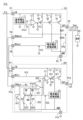
- FIG. 1 is a circuit diagram showing a configuration example of a power supply device according to a first embodiment.
- FIG. 4 is a circuit diagram showing a detailed configuration example of a power supply device according to a modified example of the first embodiment.
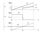
- 3 is a timing chart of currents and voltages illustrating the operation of the power supply device of FIG. 2 .
- FIG. 11 is a circuit diagram showing a configuration example of a power supply device according to a second embodiment.
- FIG. 11 is a circuit diagram showing a configuration example of a power supply device according to a third embodiment.
- FIG. 13 is a circuit diagram showing a configuration example of a power supply device according to a fourth embodiment.
- FIG. 13 is a circuit diagram showing a configuration example of a power supply device according to a fifth embodiment.
- FIG. 13 is a circuit diagram showing a configuration example of a power supply device according to a sixth embodiment. 9 is a timing chart of currents and voltages illustrating the operation of the power supply device of FIG. 8 .
- FIG. 13 is a circuit diagram showing a configuration example of a power supply device according to a seventh embodiment. 11 is a timing chart of currents and voltages illustrating the operation of the power supply device of FIG. 10.
- FIG. 13 is a circuit diagram showing a configuration example of a power supply device according to an eighth embodiment. 13 is a graph showing the relationship between each voltage and offset voltage Voffset with respect to output current Iot in the power supply device of FIG. 12. 13 is a graph showing output currents Io1 and Io2 in the power supply device of FIG.
- FIG. 13 is a graph showing output currents Io1 and Io2 in the power supply device of FIG. 12 when no offset voltage is intentionally applied, relative to the output current Iot.
- FIG. 13 is a circuit diagram showing a configuration example of a power supply device according to a ninth embodiment.
- 15 is a graph showing the relationship of the current flowing into the current-voltage conversion circuit with respect to the output current Iot in the power supply device of FIG. 14 .
- FIG. 23 is a circuit diagram showing a configuration example of a power supply device according to a tenth embodiment. 17 is a timing chart showing current and voltage in the power supply device of FIG. 16 .
- FIG. 1 is a block diagram showing a configuration of a power supply device according to a comparative example.
- FIG. 18 is a block diagram showing the configuration of a power supply device 61 according to a comparative example disclosed in Patent Document 1.
- the power supply device 61 is configured to include a voltage control unit 1 and a current control unit 2.
- the input terminal T11 of the voltage control unit 1 and the input terminal T21 of the current control unit 2 are connected to each other and to a voltage source of the input voltage Vin.
- the output terminal T13 of the voltage control unit 1 and the output terminal T23 of the current control unit 2 are connected to each other and to a load 3.
- the voltage control unit 1 and the current control unit 2 are connected in parallel to each other.
- the current detection signal output terminal T12 of the voltage control unit 1 and the current detection signal input terminal T22 of the current control unit 2 are connected to each other, and the ground terminal T14 of the voltage control unit 1 and the ground terminal T24 of the current control unit 2 are connected to each other and grounded.
- IN indicates the input terminal of the input voltage
- OUT indicates the output terminal
- BSout indicates the output terminal of the current detection signal BS1
- BSin indicates the input terminal of the current detection signal BS
- GND indicates the ground terminal.
- the input voltage Vin is input to the input terminal T11 of the voltage control unit 1 and the input terminal T21 of the current control unit 2.
- the voltage control unit 1 is a linear regulator with a built-in reference voltage generation circuit, and controls the input voltage Vin to be the reference voltage.
- a total current Iouttotal which is the sum of the output current Iout0 from the voltage control unit 1 and the output current Iout1 from the current control unit 2, flows to the load 3.
- the voltage control unit 1 also generates a current detection signal BS1, which is an analog voltage signal that corresponds to the output current Iout0 with a predetermined correlation, such as being proportional, and outputs it from the current detection signal output terminal T12 to the current detection signal input terminal T22 of the current control unit 2.
- the current control unit 2 generates a current detection signal, which is an analog voltage signal that corresponds to the output current Iout1 with a predetermined correlation, such as being proportional, and compares the current detection signal with the input current detection signal BS1 to control the difference to be substantially zero, that is, the impedance of the output transistor (e.g., corresponding to the MOS transistor Q11 in FIG. 1) that controls the output current Iout1 of the current control unit 2 is controlled so that the output current Iout0 and the output current Iout1 are, for example, equal to each other.
- the output current Iout0 and the output current Iout1 are, for example, equal to each other.
- the load 3 is, for example, an electronic device having a predetermined function that receives the power supply voltage and power supply current from the voltage control unit 1 and the current control unit 2.
- the load 3 is an electronic device for an automobile that receives power supply, or an image forming device such as a copier or printer that receives power supply, a personal computer, a tablet, a smartphone, a mobile phone, etc.
- the voltage control system in the voltage control unit 1 and the current control system in the current control unit 2 are separate, so they do not affect each other. Therefore, it is possible to realize a power supply device 61 that can establish a stable control system compared to the prior art and prevent unnecessary oscillations.
- the slave side current control unit 2 that receives the current information flows more current than the master side voltage control unit 1 that outputs the current information, the slave side current control unit 2 flows current even though the master side voltage control unit 1 tries to control the current to stop when there is no load, and the output voltage Vout rises to the input voltage Vin.
- the purpose of the embodiments of the present invention is to provide a power supply device that can solve the above problems and prevent the output voltage from rising when there is no load or a light load, and an electronic device equipped with the power supply device.
- a power supply device that can solve the above problems and prevent the output voltage from rising when there is no load or a light load, and an electronic device equipped with the power supply device.
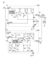
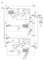
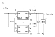
- FIG. 1 is a circuit diagram showing an example of the configuration of a power supply device 51 according to the first embodiment.
- the power supply device 51 is configured to include a voltage control unit 101 and a current control unit 201.
- the input terminal P1 (IN) of the voltage control unit 101 and the input terminals P2 (IN) of the current control unit 201 are connected to each other and to a voltage source of the input voltage Vin.
- the output terminal P2 (OUT) of the voltage control unit 101 and the output terminal P12 (OUT) of the current control unit 201 are connected to each other and to a load 301.
- the voltage control unit 101 and the current control unit 201 are connected in parallel to each other.
- the output terminal P4 (BSmout) that outputs the current detection signal (current I3) of the voltage control unit 101 and the input terminal P14 (BSmin) that inputs the current detection signal (current I3) of the current control unit 102 are connected to each other.
- the output terminal P5 (BSout) that outputs the current-voltage conversion signal (converted voltage V13) of the voltage control unit 101 and the input terminal P15 (BSin) that inputs the current-voltage conversion signal (converted voltage V13) of the current control unit 102 are connected to each other.
- the ground terminal P3 of the voltage control unit 101 and the ground terminal P13 of the current control unit 201 are connected to each other and grounded.
- the input voltage Vin is input to the input terminal P1 of the voltage control unit 101 which constitutes a reference voltage linear regulator that determines the output voltage Vout, and is also input to the input terminal P11 of the current control unit 201.
- the output current Io1 from the output terminal P2 of the voltage control unit 101 and the output current Io2 from the output terminal P12 of the current control unit 201 are added together, and then the added current Iot flows to the load 301.
- An analog current detection signal (current I3) which is detected in the voltage control unit 101 and has a correlation with the output current Io1 and corresponds, for example, in a proportional relationship, is input to the current control unit 201 via the output terminal P4 and the input terminal P14 of the current control unit 201.
- the current control unit 201 generates a current-voltage conversion signal (converted voltage V23) that has a correlation with the output current Io2 of the current control unit 201 and corresponds, for example, in a proportional relationship, and by comparing the current-voltage conversion signal (converted voltage V13) of the voltage control unit 101 with the current-voltage conversion signal (converted voltage V23) of the current control unit 201, the impedance of the output transistor Q11 of the current control unit 201 is controlled so that the output current Io1 and the output current Io2 are equal to each other.
- the current-voltage conversion signal is an example of a current detection signal, and the same applies in the following specification.
- the voltage control unit 101 is a reference voltage linear regulator and is configured with a reference voltage generation circuit 11, an operational amplifier circuit 12, a current-voltage conversion circuit 13, PMOS transistors Q1 to Q3, and voltage-dividing resistors R1 and R2.
- the reference voltage generation circuit 11 generates a predetermined reference voltage Vref based on the input voltage Vin and outputs it to the inverting input terminal of the operational amplifier circuit 12.
- the operational amplifier circuit 12 subtracts the reference voltage Vref from the feedback voltage Vfb divided by the voltage-dividing resistors R1 and R2, amplifies the result, and outputs the amplified error voltage V12 to the gates of the PMOS transistors Q1 to Q3.
- the PMOS transistor Q1 controls the output current I1 generated from the input voltage Vin based on the error voltage V12, generates the output current Io1, and outputs it from the output terminal P2 to the load 301.
- the current-voltage conversion circuit 13 converts the detection current I2 into a corresponding, for example, proportional detection voltage, and outputs it to the input terminal P15 of the current control unit 201 via the output terminal P5 as a current-voltage conversion signal (conversion voltage V13).
- the voltage-dividing resistors R1 and R2 divide the output voltage Vout generated by the output current Io1 into a feedback voltage Vfb, which is output to the non-inverting input terminal of the operational amplifier circuit 12.
- a feedback control circuit (voltage control circuit) consisting of the operational amplifier circuit 12, PMOS transistor Q1, and voltage dividing resistors R1 and R2 controls the output current I1 of the output transistor, PMOS transistor Q1, so that the divided voltage Vfb becomes the reference voltage Vref.
- the current control section 201 is configured with an operational amplifier circuit 21, a current detection circuit 22, a current-voltage conversion circuit 23, and PMOS transistors Q11 and Q12.
- the operational amplifier circuit 21 subtracts the current-voltage conversion signal (conversion voltage V13) from the current-voltage conversion signal (conversion voltage V23) from the current-voltage conversion circuit 23, amplifies the result, and outputs the error voltage V21 to the gates of the PMOS transistors Q11 and Q12.
- the PMOS transistor Q11 controls the output current I11 generated from the input voltage Vin based on the error voltage V21, generates the output current Io2, and outputs it from the output terminal P12 to the load 301.
- the current-voltage conversion circuit 23 converts the detection current I12 into a corresponding, for example proportional, detection voltage and outputs it to the non-inverting input terminal of the operational amplifier circuit 21 as a current-voltage conversion signal (converted voltage V23).
- the current detection circuit 22 When the current I3 input to the input terminal P14 is less than a predetermined third threshold current, the current detection circuit 22 generates an L-level current detection signal S22 and outputs it to the start-up control terminal of the operational amplifier circuit 21 as a non-start-up signal, while when the current I3 is equal to or greater than the third threshold current (i.e., when the output current I1 is equal to or greater than the predetermined first threshold current), it generates an H-level current detection signal S22 and outputs it to the start-up control terminal of the operational amplifier circuit 21 as a start-up signal, thereby starting up the current control circuit including the operational amplifier circuit 21 and controlling it to flow the output current of the current control unit.
- the operational amplifier circuit 21 starts up in response to
- the current detection circuit 22 is an example of a start-up control circuit.
- the start-up signal and the non-start-up signal are collectively called a start-up control signal.
- the start-up control signal is a signal generated by the start-up control circuit.
- a feedback control circuit (current control circuit) consisting of the current detection circuit 22, PMOS transistor Q12, and current-voltage conversion circuit 23 controls the output current I11 of the PMOS transistor Q11, which is an output transistor, so that the output currents Io1 and Io2 are equal to each other.
- the output current Io1 from the voltage control unit 101 and the output current Io2 from the current control unit 201 are generally set to be substantially the same.
- an offset voltage Voff is added to the operational amplifier circuit 21 due to manufacturing variations (hereinafter referred to as the first case), or if a systematic offset voltage is generated due to a predetermined gain of the feedback control circuit in the current control unit 201 (hereinafter referred to as the second case), the output currents Io1 and Io2 will no longer be substantially the same.
- the output current difference ⁇ I of the output transistors Q1 and Q11 with respect to the offset voltage Voff generated in the operational amplifier circuit 21 is expressed by the following equation.
- the current control unit 201 is provided with a current detection circuit 22, and the current detection circuit 22 controls the operational amplifier circuit 21 not to start when the output current I3 corresponding to the current I1 is less than the third threshold current. Therefore, even if an offset voltage Voff is added to the operational amplifier circuit 21, it is possible to prevent the output voltage Vout from increasing.
- the driving state of the master side voltage control unit 101 can be monitored, and the current output of the slave side current control unit 201 can be controlled to be suppressed as necessary, thereby preventing the output voltage Vout from rising to the input voltage Vin.
- the output of the output current Io2 of the slave side current control unit 201 can be stopped, thereby preventing the output voltage Vout from rising.
- the output current Io2 of the current control unit 2 is controlled so that the output current Io1 of the voltage control unit 1 and the output current Io2 of the current control unit 2 are substantially equal to each other.
- the output current Io2 of the current control unit 2 may be controlled by current dispersion so that the ratio between the output current Io1 of the voltage control unit 1 and the output current Io2 of the current control unit 2 is a predetermined value.
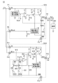
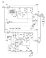
- FIG. 2 is a circuit diagram showing a detailed configuration example of a power supply device 51A according to a modification of the first embodiment, and Fig. 2 shows a detailed configuration example of a current detection circuit 22. Note that differences from Fig. 1 will be described below.
- the current detection circuit 22 is configured to include a diode-connected NMOS transistor Q13, a comparator 221, and a reference voltage generation circuit 222.
- A3 is a current-voltage conversion coefficient.
- the current I3 input to the input terminal P14 is grounded via the drain and source of the NMOS transistor Q13 and converted to a corresponding voltage V3, and the converted voltage V3 is applied to the non-inverting input terminal of the comparator 221.
- the comparator 221 compares the converted voltage V3 with the reference voltage Vref2 from the reference voltage generating circuit 222, and when V3 ⁇ Vref2, generates an L-level current detection signal S22 and outputs it to the start-up control terminal of the operational amplifier circuit 21 as a non-start-up signal, while when V3 ⁇ Vref2, generates an H-level current detection signal S22 and outputs it to the start-up control terminal of the operational amplifier circuit 21 as a start-up signal.
- the current detection signal S22 from the comparator 221 is input to the control terminal of the switch SW2 and is also input to the control terminal of the switch SW1 via the inverter INV1.
- the switches SW1 and SW2 are turned on when an H-level control signal is input to their control terminals, while they are turned off when an L-level control signal is input.
- the comparator 221 and the reference voltage generating circuit 222 are an example of a switching control circuit.
- the current control unit 201 configured as above, as the current I3 of the PMOS transistor Q3, which is the monitor transistor, increases, the drain voltage V3 of the diode-connected NMOS transistor Q13 rises. In order to detect the rise in voltage V3, the comparator 221 compares this voltage V3 with the reference voltage Vref2 of the reference voltage generating circuit 222 to generate a current detection signal S22.
- the NMOS transistor Q13 may be replaced with a series circuit of a resistor and a bias current source.
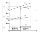
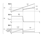
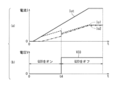
- FIG. 3 is a timing chart of currents and voltages showing the operation of the power supply device 51A in FIG. 2. The operation of the power supply device 51A in FIG. 2 will be described below with reference to FIG. 3.
- the current control unit 201 When the current control unit 201 starts at time t1 in FIG. 3, the current control unit 201 shares half of the total output current Iot (see FIG. 3(a)), and the converted voltage V13 from the current-voltage conversion circuit 13 drops. At this time, the currents Io1 and Io2 of the output transistors Q1 and Q11 are roughly the same as each other and are divided into about half of the total output current Iot, so the current I3 of the monitor transistor Q3 becomes about half of its maximum value (see FIG. 3(b)). At this time, if the threshold current Irel for the current I3 that disables the current control unit 201 is not less than half the startup detection threshold current Idet of the current control unit 201, the current control unit 201 will be disabled again.
- a hysteresis characteristic is provided so that the release threshold current Irel is less than half the startup detection threshold current Idet.
- the current detection signal S22 of the comparator 221 is used to selectively switch between the voltage sources 223 and 224, thereby selectively switching between starting and stopping the current control unit 201 with a predetermined hysteresis characteristic. This prevents unintentional release of the current control unit 201 after it has been started, thereby preventing oscillations such as chattering caused by repeated starting and stopping.
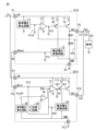
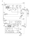
- Fig. 4 is a circuit diagram showing an example of the configuration of a power supply device 52 according to embodiment 2.
- the power supply device 52 according to embodiment 2 differs from the power supply device 51 of Fig. 1 in the following points.
- a current control unit 201A is provided instead of the current control unit 201.
- a current detection circuit 22A is provided instead of the current detection circuit 22.
- the current detection circuit 22A includes a diode-connected NMOS transistor Q14 that serves as a monitor transistor, a comparator 221, and a reference voltage generation circuit 225.
- the reference voltage generation circuit 225 generates a predetermined reference voltage Vref3 and outputs it to the inverting input terminal of the comparator 221.
- the current control section 201A further includes a PMOS transistor Q13 which is a monitor transistor.
- the source of the PMOS transistor Q13 is connected to the input terminal P11, and the gate of the PMOS transistor Q13 is connected to the output terminal of the operational amplifier circuit 21.
- the detection target of the current detection circuit 22A is the current value obtained by adding the current I13 corresponding to the output current I11 of the current control section 201A to the current I3, and the NMOS transistor Q14 converts this current value into a voltage and applies it to the non-inverting input terminal of the comparator 221.
- the current detection circuit 22A is an example of a startup control circuit.
- the power supply device 52 configured as described above, when the current control section 201A is started, the current control section 201 is responsible for generating half of the output current Io1 of the voltage control section 101, so the detection current of the monitor transistor Q3 in FIG. 1 decreases. However, since the sum of the output current Io1 of the voltage control section 101 and the output current Io2 of the current control section 201 does not change, the detection current value of the monitor transistor Q14 does not change from the detection current value of the monitor transistor Q3 before the current control section 201A was started. Therefore, the power supply device 52 according to the second embodiment has the same effect as the power supply device 51, and can suppress the oscillation phenomenon triggered by the fluctuation in the detection information accompanying the start-up of the current control section 201A.
- FIG. 5 is a circuit diagram showing an example of the configuration of a power supply device 53 according to embodiment 3.
- the power supply device 53 according to embodiment 3 differs from the power supply device 51A in Fig. 2 in the following points.
- the voltage control unit 101 is replaced with a voltage control unit 101A in which the PMOS transistor Q3 and the output terminal P4 are omitted.
- a current control unit 201B is provided in which the input terminal P14 is omitted, instead of the current control unit 201.
- the current control unit 201B further includes a reference voltage generating circuit 222 and a comparator 24, instead of the current detection circuit 22. The differences will be explained below.
- the converted voltage V13 input from the current-voltage conversion circuit 13 to the input terminal P15 is applied to the inverting input terminal of the operational amplifier circuit 21 and the non-inverting input terminal of the comparator 24.
- the reference voltage generation circuit 222 is configured in the same way as in FIG.
- the comparator 24 outputs a current detection signal S24 (the comparator 24 compares the two input voltages, so it is a voltage detection signal, but since it is originally a current detection signal corresponding to the output current of the current control unit 101A, it will be called a "current detection signal” and the same applies below) to the start control terminal of the operational amplifier circuit 21, and is input to the control terminal of the switch SW2 in the reference voltage generation circuit 222, and is also input to the control terminal of the switch SW1 via the inverter INV1.
- the switches SW1 and SW2 are turned on when an H-level control signal is input to their control terminals, and turned off when an L-level control signal is input.
- the comparator 24 is an example of a startup control circuit
- the comparator 24 and the reference voltage generating circuit 222 are an example of a switching control circuit.
- the power supply device 53 configured as above is characterized in that it performs activation determination of the current control unit 201B based on the converted voltage V13 from the current-voltage conversion circuit 13. Specifically, it is as follows.
- the comparator 24 compares the converted voltage V13 with the reference voltage Vref4 from the reference voltage generation circuit 222, and when V13 ⁇ Vref4, it generates an L-level current detection signal S24 and outputs it to the activation control terminal of the operational amplifier circuit 21 as a non-activation signal, while when V13 ⁇ Vref4, it generates an H-level current detection signal S24 and outputs it to the activation control terminal of the operational amplifier circuit 21 as a activation signal.
- the comparator 24 generates a current detection signal S24 by comparing the converted voltage V13 with the reference voltage Vref4 of the reference voltage generating circuit 222.
- the reference voltage Vref4 is selectively switched with a hysteresis characteristic to prevent chattering that repeatedly enables and disables the current control unit 201B.
- the release current needs to be less than half the detection current corresponding to the detection voltage, and the voltage values V223, V224 of the voltage sources 223, 224 are set by referring to whether or not the converted voltage V13 has become a predetermined reference voltage Vref4 and the converted voltage V13 when it becomes the release current corresponding to the predetermined release voltage.
- embodiment 3 has the same effect as embodiment 2.
- FIG. 6 is a circuit diagram showing an example of the configuration of a power supply device 54 according to embodiment 4.
- the power supply device 54 according to embodiment 4 differs from the power supply device 53 in Fig. 5 in the following points.
- a current control unit 201C is provided instead of the current control unit 201B.
- an adder circuit 25 and a reference voltage generating circuit 26 are provided instead of the reference voltage generating circuit 222. The differences will be explained below.
- the converted voltage V13 input to input terminal P15 is input to the inverting input terminal of operational amplifier circuit 21 and the first input terminal of adder circuit 25.
- the converted voltage V23 from current-voltage conversion circuit 23 is input to the second input terminal of adder circuit 25, and adder circuit 25 adds the voltages input to the two input terminals and outputs the summed voltage (V13+V23) to the non-inverting input terminal of comparator 24.
- the reference voltage generation circuit 26 generates a predetermined reference voltage Vref5 that activates or deactivates current control unit 201C and outputs it to the inverting input terminal of comparator 24.
- the comparator 24 compares the sum voltage (V13+V23) with the reference voltage Vref5, and when (V13+V23) ⁇ Vref5, it generates an L-level current detection signal S24 and outputs it to the start-up control terminal of the operational amplifier circuit 21 as a non-start-up signal, whereas when (V13+V23) ⁇ Vref5, it generates an H-level current detection signal S24 and outputs it to the start-up control terminal of the operational amplifier circuit 21 as a start-up signal.
- the voltage to be detected used to determine whether the current control unit 201C is started is the sum of the converted voltages of the current-voltage conversion circuits 13 and 23 (V13 + V23).
- the current control unit 201C takes on half of the output current Io1 of the voltage control unit 101A, so the converted voltage V13 of the current-voltage conversion circuit 13 drops.
- the current detection information does not fluctuate significantly even after the current control unit 201C is started, and the operational amplifier circuit 21 is started based on the fluctuation in the current detection information accompanying the start-up of the current control unit 201C. This prevents unintended release of the current control unit 201C after it is started, thereby making it possible to prevent oscillations such as chattering caused by repeated starting and stopping.
- Fig. 7 is a circuit diagram showing a configuration example of a power supply device 55 according to embodiment 5.
- the power supply device 55 according to embodiment 5 differs from the power supply device 51 of Fig. 1 in the following points.
- the voltage control unit 101 is replaced with a voltage control unit 101B in which the PMOS transistor Q3, the output terminal P4, and the current-voltage conversion circuit 13 are omitted.
- a current control unit 201D is provided instead of the current control unit 201.
- a reference current generation circuit 28 instead of the current detection circuit 22 and the current-voltage conversion circuit 23 of the current control unit 201, a reference current generation circuit 28, a current mirror circuit CM1, an inverter INV2, and a diode-connected NMOS transistor Q17 are provided. The differences will be explained below.
- the current I2 flowing through the PMOS transistor Q2 is input to the input terminal P15 of the current control unit 201D via the output terminal P5.
- the current mirror circuit CM1 is configured to include NMOS transistors Q15 and Q16.
- the input terminal P15 is grounded via the drain and source of the diode-connected NMOS transistor Q15, and the gate of the NMOS transistor Q15 is connected to the gate of the NMOS transistor Q16.
- the current I2 input to the input terminal P15 is converted to a voltage V13 by the NMOS transistor Q15 of the current mirror circuit CM1, and then input to the inverting input terminal of the operational amplifier circuit 21.
- the reference current generating circuit 28 generates a predetermined reference current Iref based on the input voltage Vin applied to the input terminal P11 and outputs it to the drain of the NMOS transistor Q16.
- the output terminal of the reference current generating circuit 28 is grounded via the drain and source of the NMOS transistor Q16.
- the reference current Iref from the reference current generating circuit 28 flows into the NMOS transistor Q16 of the current mirror circuit CM1, but a current I16 corresponding to the current flowing through the NMOS transistor Q15 flows out of the NMOS transistor Q16.
- the current value flowing through the NMOS transistor Q16 is Iref-I16, and a voltage V91 corresponding to the current value (Iref-I16) is generated at the drain of the NMOS transistor Q16, and the voltage V91 is input to the start-up control terminal of the operational amplifier circuit 21 via the inverter INV2 as the voltage detection signal S93, which is a start-up signal.
- the drain of the PMOS transistor Q12 is grounded via the drain and source of a diode-connected NMOS transistor Q17.
- the drain and gate of the NMOS transistor Q17 are connected to the non-inverting input terminal of the operational amplifier circuit 21.
- the inverter INV2, the reference current generating circuit 28, and the current mirror circuit CM1 are an example of a startup control circuit.
- the voltage V91 corresponding to the current value (Iref-I16) becomes less than the threshold value VINV_TH of the inverter INV2, and the voltage detection signal of the inverter INV2 goes from L level to H level. Therefore, the start-up control signal of the inverter INV2 becomes an H-level start-up signal to start up the operational amplifier circuit 21.
- the current mirror circuit CM1 copies information about the current I2 corresponding to the output current Io1 of the voltage control unit 101B to the current I16 of the current mirror circuit CM1 in the current control unit 201D, and the current I16 proportional to the output current Io1 of the voltage control unit 101B is compared with the reference current Iref, and the comparison result signal is used as a start-up control signal for the operational amplifier circuit 21.
- a current mirror circuit CM1 including a diode-connected NMOS transistor Q15 and a diode-connected NMOS transistor Q17 are used, without using the resistor-based current-voltage conversion circuits 13 and 23 of the first to fourth embodiments. This makes it possible to generate a determination circuit for the start-up control signal of the operational amplifier circuit 21 of the current control unit 201D extremely easily, without the need to prepare a separate constant voltage generation circuit or comparator, etc.
- Fig. 8 is a circuit diagram showing a configuration example of a power supply device 56 according to embodiment 6.
- Fig. 9 is a timing chart of currents and voltages showing the operation of the power supply device 56 in Fig. 8.
- the power supply device 56 differs from the power supply device 55 in Fig. 7 in the following points.
- a current control unit 201E is provided instead of the current control unit 201D.
- the reference current generating circuit 28 is replaced with a reference current generating circuit 28A.
- the reference current generating circuit 28A includes constant current sources 29a and 29b having constant currents I29a and I29b (I29a+129b>I29a), respectively, and a PMOS transistor Q29, which is a switch transistor.
- the current values in the reference current generating circuit 28A are set as follows:
- Iref_det I29a+129b (when PMOS transistor Q29 is on) (2)
- Iref_rel I29a (when PMOS transistor Q29 is off) (3)
- input terminal P11 is connected to the drain of NMOS transistor Q16 via constant current source 29a, and is also connected to the drain of NMOS transistor Q16 via constant current source 29b and the source and drain of PMOS transistor Q29.
- a current detection signal S93 from inverter INV2 is applied to the gate of NMOS transistor Q29.
- PMOS transistor Q29 is turned off in response to a high-level current detection signal S93, and turned on in response to a low-level current detection signal S93.
- the inverter INV2, the reference current generating circuit 28A, and the current mirror circuit CM1 are an example of a startup control circuit
- the inverter INV2 and the reference current generating circuit 28A are an example of a switching control circuit.
- the current control unit 201E configured as described above is characterized by selectively switching the reference current Iref to either the current I29a or the additive current (I29a+I29b) in response to the current detection signal S93.
- the current control unit 201E when the current control unit 201E is started, the current control unit 201E generates half of the total output current Iot (see Fig. 9(a)), so that the voltage V13 corresponding to the current I2 drops, and the current I16 flowing through the NMOS transistor Q16 of the current mirror circuit CM1 decreases.
- the current mirror circuit CM1 detects this at time t2, and the drain voltage V91 of the NMOS transistor Q16 goes from H level to L level.
- the start control signal S93 for controlling the enable of the operational amplifier circuit 21 goes from L level to H level.
- the reference current Iref of the reference current generating circuit 28A remains unchanged, the drain voltage V91 will change from L level to H level due to the above-mentioned action of decreasing the current of the NMOS transistor Q16 of the current mirror circuit CM1 corresponding to the output current Io1 of the voltage control unit 101B, the operational amplifier circuit 21 will be disabled, and chattering will occur as described above. Therefore, the reference current Iref from the reference current generating circuit 28A is switched from the above-mentioned formula (2) to the above-mentioned formula (3), and a hysteresis characteristic is provided in the characteristic of the voltage V91 with respect to the current I16 so that it does not fall below the release threshold.
- the current value Iref of the reference current generating circuit 280 is set to a current value Iref_rel that is less than half the normal value as shown in FIG. 9(c) in response to the current detection signal S93 of the operational amplifier circuit 21 changing from L level to H level.
- the power supply device 56 according to the sixth embodiment has the same effect as that of the fifth embodiment, and furthermore, by preventing unintended deactivation after the current control unit 201E is activated, it is possible to prevent oscillation caused by repeated activation and deactivation.
- Fig. 10 is a circuit diagram showing a configuration example of a power supply device 57 according to embodiment 7.
- Fig. 11 is a timing chart of currents and voltages showing the operation of the power supply device of Fig. 10.
- the power supply device 57 according to embodiment 7 differs from the power supply device 55 of Fig. 7 in the following points.
- a current control unit 201F is provided instead of the current control unit 201D.
- the current control unit 201F further includes an NMOS transistor Q18, and the NMOS transistor Q18 and the NMOS transistor Q17 form a current mirror circuit CM2. The differences will be explained below.
- the gates and sources of the diode-connected NMOS transistor Q17 and NMOS transistor Q18 are connected to each other to form a current mirror circuit CM2.
- the current control unit 201F in FIG. 10 is different from the embodiment 5 in FIG. 7 in that the detection target current of the current detection signal S93 used to determine the start-up of the current control unit 201F is the sum of the current I16 of the NMOS transistor Q16 in the current mirror circuit CM1 and the current I18 of the NMOS transistor Q18 in the current mirror circuit CM2.
- the inverter INV2, the reference current generating circuit 28, and the current mirror circuits CM1 and CM2 are an example of a startup control circuit.
- the current control unit 201F takes over half of the total output current Iot, so the current I16 decreases.
- the sum current Iot of the output currents Io1 and Io2 of the voltage control unit 101B and current control unit 201F does not change (see FIG. 11(a))
- the sum of the currents of the current mirror circuits CM1 and CM2 which are correlated with the sum of the output current information of the control units 101B and 201F, does not change.
- the same effect as that of the sixth embodiment is obtained, and since the current detection information does not fluctuate significantly even after the current control unit 201F is started, it is possible to suppress the oscillation phenomenon triggered by the fluctuation in the current detection information accompanying the start-up of the current control unit 201F.
- Fig. 12 is a circuit diagram showing a configuration example of a power supply device 58 according to embodiment 8.
- the power supply device 58 according to embodiment 8 differs from the power supply device 53 of Fig. 5 in the following points.
- a current control unit 201G is provided instead of the current control unit 201B.
- the current control unit 201G is provided with an offset voltage source 30 having an offset voltage V30 instead of the reference voltage generation circuit 222 and the comparator 24. Note that the current detection signal that is the start-up control signal to the operational amplifier circuit 21 is not used. The differences will be explained below.
- an offset voltage source 30 is provided at the non-inverting input terminal of the operational amplifier circuit 21 so that the output current Io2 of the current control section 201 is intentionally lower than the output current Io1 of the voltage control section 101A.
- the sum of the converted voltage V23 from the current-voltage conversion circuit 23 and the offset voltage Voffset is applied to the non-inverting input terminal of the operational amplifier circuit 21.
- the phenomenon in which the output voltage Vout rises to the input voltage Vin of the input terminal T1 occurs because the current control unit 201 passes the output current Io2 even though the voltage control unit 101 tries to hold the output voltage Vout by stopping the output current Io1.
- an offset voltage is applied so that the operational amplifier circuit 21 controls the voltage to a level higher than the voltage of its non-inverting input terminal, which causes the above phenomenon to become apparent.
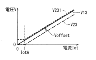
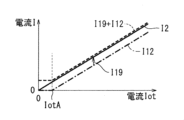
- FIG. 13A is a graph showing the relationship between each voltage and offset voltage Voffset for output current Iot in power supply device 58 of FIG. 12.
- FIG. 13B is a graph showing output currents Io1 and Io2 for output current Iot in power supply device 58 of FIG. 12 when there is an intentionally applied offset voltage Voffset.
- FIG. 13C is a graph showing output currents Io1 and Io2 for output current Iot in power supply device 58 of FIG. 12 when there is no intentionally applied offset voltage Voffset.
- an offset voltage source 30 is provided in the operational amplifier circuit 21, so that the converted voltage V23 is controlled to be lower than the converted voltage V13 as shown in FIG. 13A, and the output current Io2 of the current control unit 201G is cut off when there is no load.
- the transistor Q1 in the voltage control unit 101A flows an output current Iot1 equal to or greater than a certain level, and until the converted voltage V13 becomes larger than the offset voltage source 30, the voltage V231 on the non-inverting input terminal side of the operational amplifier circuit 21 becomes higher, so that the PMOS transistor Q12 and the output transistor Q11 are controlled to be turned off.
- the offset voltage source 30 prevents the current control unit 201G from starting unnecessarily when there is no load, and prevents the output voltage Vout from rising, even without providing a circuit to stop the operational amplifier circuit 21.
- the offset voltage source 30 corresponds to a component of a part of the start-up control circuit of the above-mentioned embodiments 1 to 7.
- Fig. 14 is a circuit diagram showing a configuration example of a power supply device 59 according to embodiment 9.
- the power supply device 59 according to embodiment 9 differs from the power supply device 58 according to embodiment 8 in Fig. 12 in the following points.
- a current control unit 201H is provided instead of the current control unit 201G.
- a bias voltage generating circuit 31 and a PMOS transistor Q19 are provided. The differences will be explained below.
- an input terminal P11 of a current control section 201H is connected to an input terminal of a current-voltage conversion circuit 23 via the source and drain of a PMOS transistor Q19, which is a bias transistor.
- a bias voltage generation circuit 31 generates a predetermined bias voltage Vbias and applies it to the gate of the PMOS transistor Q19.
- the PMOS transistor Q19 generates a current I19 corresponding to the bias voltage Vbias and causes it to flow into the current-voltage conversion circuit 23.
- FIG. 15 is a graph showing the relationship between the output current Iot and the current flowing into the current-voltage conversion circuits 13 and 23 in the power supply device 59 of FIG. 14.
- the current I2 detected by the current-voltage conversion circuit 13 (current detection circuit) of the voltage control unit 101A becomes smaller than the bias current I19 by the bias voltage generation circuit 31, and the converted voltage V23 becomes larger than the converted voltage V13, so that the PMOS transistor Q12 and the output transistor Q11 are controlled to be turned off.
- the bias voltage generating circuit 31 and the PMOS transistor Q19 are provided.
- the bias voltage generating circuit 31 causes the operational amplifier circuit 21 to recognize that the current control unit 201H is passing a larger current than the voltage control unit 101A, and an offset is applied so that the current control unit 201H tends to reduce the output current Io2. Therefore, the power supply device 59 according to the ninth embodiment has the same effect as the power supply device 58 according to the eighth embodiment.
- FIG. 16 is a circuit diagram showing a configuration example of a power supply device 60 according to embodiment 10.
- the power supply device 60 according to embodiment 10 differs from the power supply device 59 according to embodiment 9 in Fig. 14 in the following points.
- a current control unit 201I is provided instead of the current control unit 201H.
- the current control unit 201I further includes a reference voltage generating circuit 32, a comparator 33, and a PMOS transistor Q20. The differences will be explained below.
- the input terminal P11 of the current control unit 201I is connected to the input terminal of the current-voltage conversion circuit 23 via the source and drain of the PMOS transistor Q19 and the source and drain of the PMOS transistor Q20.
- the converted voltage V13 input to the input terminal P15 is input to the non-inverting input terminal of the operational amplifier circuit 21 and the non-inverting input terminal of the comparator 33.
- the reference voltage generation circuit 32 outputs a predetermined reference voltage Vref6 to the inverting input terminal of the comparator 33.
- the comparator 33 applies an L-level current detection signal S33 to the gate of the PMOS transistor Q20 to turn on the PMOS transistor Q20, thereby allowing the offset current I19 to flow.
- the comparator 33 applies an H-level current detection signal S33 to the gate of the PMOS transistor Q20 to turn off the PMOS transistor Q20, thereby preventing the offset current I19 from flowing.
- NMOS transistor Q20, comparator 33, and reference voltage generating circuit 32 are an example of a switching control circuit.
- the current control unit 201I configured as described above is characterized in that the start-up control of the operational amplifier circuit 21 by the comparator 24 of the power supply device 53 in FIG. 5 is realized by the reference voltage of the operational amplifier circuit 21 by current control of the PMOS transistor Q20.
- FIG. 17 is a timing chart showing the current and voltage in the power supply device 60 of FIG. 16.
- the voltage detection signal S33 of the comparator 33 goes to L level, and by turning on the PMOS transistor Q20, an offset current I19 is added so that the output current Io2 of the current control unit 201I is smaller than the output current Io1 of the voltage control unit 101A.
- the offset current I19 of the current control unit 201I is not allowed to flow. This suppresses bias in the output current when the output current is equal to or higher than a certain threshold value.
- the output current Io2 of the current control unit 201I is reduced so that the output voltage Vout does not rise, and when a predetermined threshold output current begins to flow, the PMOS transistor Q20 is turned off, thereby adjusting the current balance of each control unit 101A, 201I, thereby preventing current imbalance during heavy load when the influence of heat generation is significant.
- the power supply device of the present invention can monitor the operating state of the master voltage control unit and, if necessary, control the slave current control unit to suppress the current output, thereby preventing the output voltage from rising to the input voltage.
- An electronic device may be configured with the power supply devices 51 to 60 according to the embodiments and the load 301.
- the electronic device may be, for example, an electronic device for an automobile that receives power supply, or an image forming device such as a copier or printer that receives power supply, a personal computer, a tablet, a smartphone, a mobile phone, etc.
Landscapes
- Engineering & Computer Science (AREA)
- Physics & Mathematics (AREA)
- Electromagnetism (AREA)
- General Physics & Mathematics (AREA)
- Radar, Positioning & Navigation (AREA)
- Automation & Control Theory (AREA)
- Continuous-Control Power Sources That Use Transistors (AREA)
Abstract
Est fourni un dispositif d'alimentation capable apte à empêcher une tension de sortie de s'élever lorsqu'aucune charge n'est appliquée. Ce dispositif d'alimentation électrique comprend une unité de commande de tension et une unité de commande de courant qui sont connectées en parallèle l'une à l'autre. L'unité de commande de tension comprend : un circuit de tension de référence qui génère une tension de référence prédéterminée sur la base d'une tension d'entrée ; et un circuit de commande de tension qui commande le courant de sortie de l'unité de commande de tension de sorte que la tension de sortie de l'unité de commande de tension est sensiblement une tension correspondant à la tension de référence, générant et délivrant ainsi la tension de sortie de l'unité de commande de tension sur la base de la tension d'entrée. L'unité de commande de courant comprend : un circuit de détection de courant qui détecte le courant de sortie de l'unité de commande de courant et génère et délivre en sortie un signal de détection de courant indiquant une valeur correspondant au courant de sortie ; un circuit de commande de courant qui commande le courant de sortie de l'unité de commande de courant de sorte que le signal de détection de courant soit sensiblement une valeur correspondant à la valeur de courant de sortie de l'unité de commande de tension ; et un circuit de commande de démarrage qui réalise une commande pour démarrer le circuit de commande de courant lorsque le courant de sortie de l'unité de commande de tension devient égal ou supérieur à un seuil prédéterminé de manière à amener le courant de sortie de l'unité de commande de courant à s'écouler.
Priority Applications (1)
| Application Number | Priority Date | Filing Date | Title |
|---|---|---|---|
| PCT/JP2023/030164 WO2025041267A1 (fr) | 2023-08-22 | 2023-08-22 | Dispositif d'alimentation électrique et appareil électronique |
Applications Claiming Priority (1)
| Application Number | Priority Date | Filing Date | Title |
|---|---|---|---|
| PCT/JP2023/030164 WO2025041267A1 (fr) | 2023-08-22 | 2023-08-22 | Dispositif d'alimentation électrique et appareil électronique |
Publications (1)
| Publication Number | Publication Date |
|---|---|
| WO2025041267A1 true WO2025041267A1 (fr) | 2025-02-27 |
Family
ID=94731532
Family Applications (1)
| Application Number | Title | Priority Date | Filing Date |
|---|---|---|---|
| PCT/JP2023/030164 Pending WO2025041267A1 (fr) | 2023-08-22 | 2023-08-22 | Dispositif d'alimentation électrique et appareil électronique |
Country Status (1)
| Country | Link |
|---|---|
| WO (1) | WO2025041267A1 (fr) |
Citations (5)
| Publication number | Priority date | Publication date | Assignee | Title |
|---|---|---|---|---|
| JP2002125371A (ja) * | 2000-10-16 | 2002-04-26 | Sharp Corp | 多出力電源装置及びそれを備えた電子機器 |
| JP2005176409A (ja) * | 2003-12-08 | 2005-06-30 | Matsushita Electric Ind Co Ltd | 直流電源装置 |
| JP2006133935A (ja) * | 2004-11-04 | 2006-05-25 | Rohm Co Ltd | 電源装置、及び携帯機器 |
| JP2015146699A (ja) * | 2014-02-04 | 2015-08-13 | 三菱電機株式会社 | 電源装置 |
| JP7170935B2 (ja) * | 2020-03-18 | 2022-11-14 | 日清紡マイクロデバイス株式会社 | 電源装置及び電子機器 |
-
2023
- 2023-08-22 WO PCT/JP2023/030164 patent/WO2025041267A1/fr active Pending
Patent Citations (5)
| Publication number | Priority date | Publication date | Assignee | Title |
|---|---|---|---|---|
| JP2002125371A (ja) * | 2000-10-16 | 2002-04-26 | Sharp Corp | 多出力電源装置及びそれを備えた電子機器 |
| JP2005176409A (ja) * | 2003-12-08 | 2005-06-30 | Matsushita Electric Ind Co Ltd | 直流電源装置 |
| JP2006133935A (ja) * | 2004-11-04 | 2006-05-25 | Rohm Co Ltd | 電源装置、及び携帯機器 |
| JP2015146699A (ja) * | 2014-02-04 | 2015-08-13 | 三菱電機株式会社 | 電源装置 |
| JP7170935B2 (ja) * | 2020-03-18 | 2022-11-14 | 日清紡マイクロデバイス株式会社 | 電源装置及び電子機器 |
Similar Documents
| Publication | Publication Date | Title |
|---|---|---|
| KR101136691B1 (ko) | 정전압 회로 | |
| JP5027189B2 (ja) | 電源レギュレータ | |
| US9141121B2 (en) | Voltage regulator | |
| US8169202B2 (en) | Low dropout regulators | |
| KR101004851B1 (ko) | 출력 제어 기능을 갖는 전력증폭기 시스템 | |
| US8729876B2 (en) | Voltage regulator and related voltage regulating method thereof | |
| US10250128B2 (en) | Type III switching converter error amplifier with fast transient response behavior | |
| EP1258982B1 (fr) | Montage amplificateur opérationnel avec un circuit de commande du courant de repos | |
| US6771122B2 (en) | DC offset compensation circuit of closed loop operational amplifier and method of compensating for DC offset | |
| CN113141113B (zh) | 具有自适应补偿的开关转换器 | |
| US20190068055A1 (en) | Switching regulator | |
| JP7170935B2 (ja) | 電源装置及び電子機器 | |
| CN107508462A (zh) | 针对负载的切换控制器和方法 | |
| WO2025041267A1 (fr) | Dispositif d'alimentation électrique et appareil électronique | |
| CN110677025A (zh) | 调压器的电流限制 | |
| CN113748393A (zh) | 恒压电路以及电子设备 | |
| CN113273069B (zh) | 利用内部模拟控制环路向负载供电的电源和方法 | |
| US20180212691A1 (en) | Semiconductor integrated circuit, semiconductor system, and electric source voltage control method | |
| US7855542B2 (en) | Voltage regulator startup method and apparatus | |
| JP2007303986A (ja) | 直流試験装置 | |
| US11463058B2 (en) | Feedback system and associated signal processing method | |
| CN113568464B (zh) | 偏压补偿装置及操作偏压补偿装置的方法 | |
| US11385668B2 (en) | Configurable offset compensation device | |
| JP5008581B2 (ja) | 安定化電源回路 | |
| CN121277286A (zh) | 基于比较器的电压调节系统和运行电压调节系统的方法 |
Legal Events
| Date | Code | Title | Description |
|---|---|---|---|
| 121 | Ep: the epo has been informed by wipo that ep was designated in this application |
Ref document number: 23949728 Country of ref document: EP Kind code of ref document: A1 |
|
| ENP | Entry into the national phase |
Ref document number: 2025541219 Country of ref document: JP Kind code of ref document: A |
|
| WWE | Wipo information: entry into national phase |
Ref document number: 2025541219 Country of ref document: JP |
|
| NENP | Non-entry into the national phase |
Ref country code: DE |