WO2021172032A1 - 弾性波デバイス - Google Patents
弾性波デバイス Download PDFInfo
- Publication number
- WO2021172032A1 WO2021172032A1 PCT/JP2021/005129 JP2021005129W WO2021172032A1 WO 2021172032 A1 WO2021172032 A1 WO 2021172032A1 JP 2021005129 W JP2021005129 W JP 2021005129W WO 2021172032 A1 WO2021172032 A1 WO 2021172032A1
- Authority
- WO
- WIPO (PCT)
- Prior art keywords
- film
- wavelength
- thickness
- wave device
- acoustic
- Prior art date
- Legal status (The legal status is an assumption and is not a legal conclusion. Google has not performed a legal analysis and makes no representation as to the accuracy of the status listed.)
- Ceased
Links
Images







Classifications
-
- H—ELECTRICITY
- H03—ELECTRONIC CIRCUITRY
- H03H—IMPEDANCE NETWORKS, e.g. RESONANT CIRCUITS; RESONATORS
- H03H9/00—Networks comprising electromechanical or electro-acoustic elements; Electromechanical resonators
- H03H9/02—Details
- H03H9/02535—Details of surface acoustic wave devices
- H03H9/02543—Characteristics of substrate, e.g. cutting angles
- H03H9/02559—Characteristics of substrate, e.g. cutting angles of lithium niobate or lithium-tantalate substrates
-
- H—ELECTRICITY
- H03—ELECTRONIC CIRCUITRY
- H03H—IMPEDANCE NETWORKS, e.g. RESONANT CIRCUITS; RESONATORS
- H03H9/00—Networks comprising electromechanical or electro-acoustic elements; Electromechanical resonators
- H03H9/02—Details
- H03H9/02535—Details of surface acoustic wave devices
- H03H9/02543—Characteristics of substrate, e.g. cutting angles
- H03H9/02574—Characteristics of substrate, e.g. cutting angles of combined substrates, multilayered substrates, piezoelectrical layers on not-piezoelectrical substrate
-
- H—ELECTRICITY
- H03—ELECTRONIC CIRCUITRY
- H03H—IMPEDANCE NETWORKS, e.g. RESONANT CIRCUITS; RESONATORS
- H03H9/00—Networks comprising electromechanical or electro-acoustic elements; Electromechanical resonators
- H03H9/02—Details
- H03H9/125—Driving means, e.g. electrodes, coils
- H03H9/145—Driving means, e.g. electrodes, coils for networks using surface acoustic waves
-
- H—ELECTRICITY
- H03—ELECTRONIC CIRCUITRY
- H03H—IMPEDANCE NETWORKS, e.g. RESONANT CIRCUITS; RESONATORS
- H03H9/00—Networks comprising electromechanical or electro-acoustic elements; Electromechanical resonators
- H03H9/25—Constructional features of resonators using surface acoustic waves
Definitions
- the present invention relates to an elastic wave device.
- the 5th generation mobile communication system is using the frequency band of 3.3 GHz to 4.9 GHz, and the next generation is planned to use the frequency band of 6 GHz or higher. ing.
- FBAR Film Bulk Acoustic Resonator
- SAW Surface acoustic wave
- LN three crystals
- LT LiTaO three crystals
- LLSAW longitudinal wave leakage elastic waves
- SAW surface acoustic wave
- the vibration mode of the bulk wave used is only the thickness longitudinal vibration.
- the sound velocity of this longitudinal wave is represented by (c33 D / density) 1/2 (c33 D is the elastic stiffness constant), and the excitation frequency is set to the value represented by sound velocity / (2 x film thickness) of the electrode.
- the frequency is obtained by subtracting the frequency decrease due to the mass load. Therefore, in order to increase the excitation frequency to a high frequency, the film thickness of the piezoelectric thin film must be extremely thin.
- those using AlN or ScAlN as the piezoelectric thin film have large attenuation at ultra-high frequencies because they are polycrystalline thin films, and it is difficult to realize good characteristics.
- a piezoelectric film such as ZnO When a piezoelectric film such as ZnO is formed on a high-frequency substrate such as sapphire, a Rayleigh wave (0th order) in the basic mode and a Sezawa wave (sezawa wave in the higher order mode) are used according to the thickness of the piezoelectric film.
- the waves of the primary) and its higher mode (secondary, tertiary, ...) Are excited, but the frequency of the higher mode is not an integral multiple of the frequency of the basic mode.
- an overtone having a frequency (Harmonic frequency) that is an integral multiple of about 2 times, 3 times, and so on is excited.
- the SAW that is excited about twice, three times, and so on in the basic mode in this way is also referred to as an overtone below.
- asymmetrical Lamb wave of the zero-order mode (A 0 mode) is sound velocity slows as the substrate becomes thinner, A 1 Mode 1 order mode of higher order faster reversed , The ratio varies greatly depending on the thickness of the piezoelectric substrate. Moreover, the two are not in an integral multiple relationship. As Sezawa wave described above, A 1 mode is a higher order mode A 0 mode, not the overtone.
- the limit of SAW devices is about 3.2 GHz on the high frequency side, but other than SAW, there are reports of high frequency devices of 3.2 GHz or higher using surface acoustic waves.
- SV shear vertical
- SH type SH 0 mode with a shear horizontal (SH) component There is a shear wave.
- a high sound velocity of 6,000 m / s which is about 1.5 times that of SAW, can be obtained in S 0 mode, and about 3 to 6 times in A 1 mode.
- a high sound velocity of 12,000 to 25,000 m / s can be obtained, which is advantageous for the realization of a high-frequency device. Therefore, 0.34 using a fundamental wave of A 1 Mode LN or LT in the thin film of ⁇ 0.48 .mu.m, 4.5 resonators devices ⁇ 6.3 GHz is realized (for example, Non-Patent Document 5 or 6 reference).
- this device requires cavities in both the upper and lower portions of the IDT portion on the piezoelectric thin plate that excites the sheet wave, there is a big problem that the mechanical strength is weak in the thin plate of 0.48 ⁇ m or less.
- Non-Patent Documents 1 and 2 have a problem that good characteristics with a large impedance ratio cannot be obtained in an ultra-high frequency band of 6 GHz or higher.
- devices using conventional surface acoustic waves (SAW) and longitudinal wave leakage elastic waves (LLSAW) form a blind electrode (IDT) on a piezoelectric thin film.
- SAW surface acoustic waves
- LLSAW longitudinal wave leakage elastic waves
- IDT blind electrode
- a 1 mode plate wave is acoustic velocity which is determined by the anti-resonance frequency of the fundamental mode has a 15,500m / s, the speed of sound, A 1 mode Lamb of There was a problem that it was the speed of sound in the basic mode, not the speed of sound in overtone. Further, in the device described in Non-Patent Document 5, 6 and 7, the azimuthal angle, irrespective of the substrate thickness, the acoustic velocity of the S 0 mode LiNbO 3 (LN) or LiTaO 3 (LT) is 6,000 to 7, Although it is 000 m / s, there is a problem that this also does not use overtone.
- the sound velocity of the SH 0 mode plate wave device described in Patent Documents 1 and 2 is not described, but in the devices described in Non-Patent Documents 5, 6 and 7, regardless of the azimuth angle and the substrate thickness.
- the speed of sound of the SH 0 mode plate wave of LN and LT is about 4,000 m / s.
- the present invention has been made focusing on such a problem, and an object of the present invention is to provide an elastic wave device capable of obtaining good characteristics in an ultra-high frequency band of 6 GHz or more by using overtone. do.
- the surface acoustic wave device includes a piezoelectric substrate, an electrode provided in contact with the piezoelectric substrate, and an acoustic multilayer film provided in contact with the piezoelectric substrate and / or the electrode. It is characterized in that it is configured to utilize the overtone of the resonance characteristics of surface acoustic waves.
- the elastic wave device can excite an overtone of about an integral multiple (about 2 times, about 3 times, ...) The frequency of the basic mode of the surface acoustic wave by the acoustic multilayer film. Further, by adjusting the thickness of the electrode, the type of the piezoelectric substrate, and the thickness of each layer of the acoustic multilayer film, it is possible to obtain an overtone of a surface acoustic wave having a large impedance ratio. By utilizing this overtone, the elastic wave device according to the present invention can obtain good characteristics having a large impedance ratio in an ultra-high frequency band of 6 GHz or more.
- This surface acoustic wave of overtone corresponds to, for example, a sound velocity of 9000 m / s or more, and in some cases, 10,000 m / s or more.
- the impedance ratio (Impedance ratio) of the elastic wave device is the ratio [20 ⁇ log (Za / Zr)] of the resonance impedance Zr at the resonance frequency fr and the antiresonance impedance Za at the antiresonance frequency fa. ..
- the band width of the elastic wave device is (fa-fr) / fr.
- the low acoustic impedance film and the high acoustic impedance film are alternately laminated in the acoustic multilayer film.
- the acoustic multilayer film has an acoustic film in which low acoustic impedance films and high acoustic impedance films are alternately and continuously laminated in 3 or more and 20 or less layers.
- the thicknesses of at least three layers of the low acoustic impedance film and the high acoustic impedance film of the acoustic multilayer film are 0.012 wavelength to 0.118 wavelength of the elastic surface wave, respectively.
- the thickness of one of the combination of the low acoustic impedance film and the high acoustic impedance film of the acoustic multilayer film is 0.012 wavelength to 0.118 wavelength, or 0.02 wavelength to 0.12 wavelength. , Or more preferably 0.03 wavelength to 0.082 wavelength.
- each low acoustic impedance film and / or each high acoustic impedance film of the acoustic multilayer film is made of Mg alloy, SiO 2 , SiOF, Al, Y, Si, Ge, Ti, ZnO, Si.
- the low acoustic impedance film may be made of a film having a smaller acoustic impedance than the adjacent high acoustic impedance film.
- the acoustic impedance Zl in the longitudinal wave and the acoustic impedance Zs in the transverse wave of each low acoustic impedance film and each high acoustic impedance film are (density ⁇ c33) 1/2 and, respectively. (Density x c44) It is represented by 1/2 (c33 and c44 are elastic stiffness constants).
- the smaller Z1 or the smaller Zs is the low acoustic impedance film, and the larger one is the high acoustic impedance film.
- the piezoelectric substrate is preferably made of a single crystal of LiNbO 3 or LiTaO 3. In this case, it is easy to excite the overtone of the surface acoustic wave.
- the electrode in order to obtain a large impedance ratio, is composed of a drooping electrode provided on one surface of the piezoelectric substrate, and the acoustic multilayer film is the other of the piezoelectric substrate.
- the piezoelectric substrate is composed of LiNbO 3 crystals with Euler angles (-30 ° to 30 °, 60 ° to 103 °, -15 ° to 15 °) and (90 ° ⁇ 6 °,). It is preferable that the Euler angles are crystallically equivalent to any one of 90 ° ⁇ 6 ° and ⁇ 20 ° to 48 °) or any one of them.
- the piezoelectric substrate has Euler angles of (-30 ° to 30 °, 72 ° to 97 °, -15 ° to 15 °) and (90 ° ⁇ 6 °, 90 ° ⁇ 6 °, -10 °). It is more preferable that the Euler angles are crystallographically equivalent to any one of ( ⁇ 43 °) or any one of them. Further, in this case, the piezoelectric substrate has Euler angles of (-30 ° to 30 °, 78 ° to 92 °, -6 ° to 6 °) and (90 ° ⁇ 6 °, 90 ° ⁇ 6 °, -2 °). It is more preferable that the Euler angles are crystallographically equivalent to any one of ( ⁇ 33 °) or any one of them.
- the electrodes are provided so as to cover the electrode-shaped electrode provided on one surface of the piezoelectric substrate and the other surface of the piezoelectric substrate. and a floating electrode, the acoustic multi-layer film, wherein the said piezoelectric substrate floating electrode is provided so as to contact the surface of the opposite side, the piezoelectric substrate is made of LiNbO 3 crystal, Euler angles (-30 ° ⁇ 30 °, 64 ° ⁇ 98 °, -15 ° ⁇ 15 °) and (90 ° ⁇ 6 °, 90 ° ⁇ 6 °, -4 ° ⁇ 56 °), or one of these It is preferable that the oiler angle is crystallically equivalent to.
- the piezoelectric substrate has Euler angles of (-30 ° to 30 °, 68 ° to 95 °, -15 ° to 15 °) and (90 ° ⁇ 6 °, 90 ° ⁇ 6 °, -2 °). It is more preferable that the Euler angles are crystallographically equivalent to any one of ( ⁇ 52 °) or any one of these. Further, in this case, the piezoelectric substrate has Euler angles of (-30 ° to 30 °, 72 ° to 92 °, -15 ° to 15 °) and (90 ° ⁇ 6 °, 90 ° ⁇ 6 °, 25 ° to). It is more preferable that the Euler angles are crystallographically equivalent to either one of these (50 °) or any one of them.
- the floating electrode may be connected to one of the blind electrodes or a common electrode other than the elastic wave device according to the present invention.
- the thickness of the piezoelectric substrate is preferably 0.002 to 5 wavelengths of the surface acoustic wave, more preferably 1.2 wavelengths or less, and 0.02 to 0. .3 wavelengths are more preferred. In this case, a larger impedance ratio can be obtained.
- the electrode in order to obtain a large impedance ratio, is composed of a drooping electrode provided on one surface of the piezoelectric substrate, and the acoustic multilayer film is the other of the piezoelectric substrate.
- the piezoelectric substrate is composed of LiTaO 3 crystals and has Euler angles (-30 ° to 30 °, 55 ° to 100 °, -15 ° to 15 °), (90 ° ⁇ 6 °,).
- the piezoelectric substrate has Euler angles (-30 ° to 30 °, 61 ° to 95 °, -15 ° to 15 °), (90 ° ⁇ 6 °, 90 ° ⁇ 6 °, 15 ° to). 55 °) and (90 ° ⁇ 6 °, 90 ° ⁇ 6 °, 85 ° to 91 °), or Euler angles that are crystallographically equivalent to any one of these. preferable.
- the piezoelectric substrate has Euler angles of (-30 ° to 30 °, 70 ° to 89 °, -15 ° to 15 °) and (90 ° ⁇ 6 °, 90 ° ⁇ 6 °, 23 ° to). It is more preferable that the Euler angles are crystallographically equivalent to either one of 38 °) or any one of these.
- the electrodes are provided so as to cover the electrode-shaped electrode provided on one surface of the piezoelectric substrate and the other surface of the piezoelectric substrate. It has a floating electrode, and the acoustic multilayer film is provided so as to be in contact with the surface of the floating electrode opposite to the piezoelectric substrate.
- the piezoelectric substrate is composed of LiTaO 3 crystals and has an oiler angle of (-30 °).
- the piezoelectric substrate has Euler angles of (-30 ° to 30 °, 69 ° to 91 °, -15 ° to 15 °) and (90 ° ⁇ 6 °, 90 ° ⁇ 6 °, -2 °). It is more preferable that the Euler angles are crystallographically equivalent to any one of ( ⁇ 52 °) or any one of these.
- the piezoelectric substrate has Euler angles (90 ° ⁇ 6 °, 90 ° ⁇ 6 °, 25 ° to 50 °) or crystallographically equivalent Euler angles. ..
- the floating electrode may be connected to one of the blind electrodes or a common electrode other than the elastic wave device according to the present invention.
- the thickness of the piezoelectric substrate is preferably 0.002 to 2.4 wavelengths of the surface acoustic wave, more preferably 1 wavelength or less, and 0.02 to 0. It is more preferably 25 wavelengths. In this case, a larger impedance ratio can be obtained.
- the blind electrode has a density of 1800 kg / m 3 or more and less than 6000 kg / m 3 and a thickness, where MR is the metallization ratio and ⁇ is the wavelength of the elastic surface wave.
- the thickness Is (0.01 ⁇ ⁇ 0.045 ⁇ ) ⁇ 0.5 / MR or (0.1 ⁇ ⁇ 0.21 ⁇ ) ⁇ 0.5 / MR or a density of less than 6000 kg / m 3 or more 10000 kg / m 3,
- the thickness Is (0.01 ⁇ to 0.033 ⁇ ) x 0.5 / MR or (0.06 ⁇ to 0.2 ⁇ ) x 0.5 / MR, or the density is 10000 kg / m 3 or more and less than 15000 kg / m 3
- the thickness is Is (0.008 ⁇ to 0.03 ⁇ ) x 0.5 / MR or (0.055 ⁇ to 0.19 ⁇ ) x 0.5 / MR, or the density is 15000 kg / m 3 or more and less than 25000 kg / m 3
- the thickness is Is preferably (0.005 ⁇ to 0.02 ⁇ ) ⁇ 0.5 / MR or (0.062 ⁇ to 0.165 ⁇ ) ⁇ 0.5 / MR.
- Euler angles ( ⁇ , ⁇ , ⁇ ) are right-handed systems and represent the cut surface of the piezoelectric substrate and the propagation direction of elastic waves. That is, with respect to the crystals constituting the piezoelectric substrate and the crystal axes X, Y, and Z of LT or LN, the X axis is rotated by ⁇ counterclockwise with the Z axis as the rotation axis to obtain the X'axis. Next, the X'axis is used as the rotation axis, and the Z axis is rotated by ⁇ counterclockwise to obtain the Z'axis. At this time, the Z'axis is the normal line, and the surface including the X'axis is the cut surface of the piezoelectric substrate.
- the direction in which the Z'axis is the rotation axis and the X'axis is ⁇ -rotated counterclockwise is defined as the propagation direction of the elastic wave.
- the axes perpendicular to the X'axis and the Z'axis obtained by moving the Y axis by these rotations are defined as the Y'axis.
- (0 °, ⁇ + 180 °, 0 °) is not equivalent to (0 °, ⁇ , 0 °) in terms of Euler angles, but is related to the front and back of the substrate.
- the elastic wave device shows the same characteristics on the front and back sides, the orientation of the relationship between the front and back sides of the substrate is also regarded as an equivalent surface here.
- an elastic wave device capable of obtaining good characteristics in an ultra-high frequency band of 6 GHz or more by using overtone.
- the relationship between the impedance ratio in the structure of the substrate and (a) the W film thickness of the high acoustic impedance film at an Al film thickness of 0.05 ⁇ and (b) the Al film thickness of the low acoustic impedance film at a W film thickness of 0.05 ⁇ is shown. It is a graph. Cu (0.1 ⁇ ) / (90 °, 90 °, ⁇ ) LN (0.2 ⁇ ) / Al (0.05 ⁇ ) / W (0.05 ⁇ ) / Al (0.05 ⁇ ) of the elastic wave device shown in FIG.
- the blind electrode / (90 °, 90 °, 35 °) LT (0.15 ⁇ ) / floating electrode / SiO 2 (0.05 ⁇ ) / Ta (0.05 ⁇ ) / SiO 2 (0.05 ⁇ ) / Ta (0.05 ⁇ ) / SiO 2 (0.05 ⁇ ) / Ta (0.05 ⁇ ) / SiO 2 (0.05 ⁇ ) / Ta (0.05 ⁇ ) / Si
- the impedance ratio in the substrate structure and the thickness of each electrode at MR 0.5 (Electrode thickness). It is a graph which shows the relationship with. Cu (0.1 ⁇ ) / (90 °, 90 °, 42.5 °) LN (0.2 ⁇ ) / floating electrode / SiO 2 (0.05 ⁇ ) / Ta (0.05 ⁇ ) / of the elastic wave device shown in FIG. 1 (b).
- the elastic wave device 10 is configured to utilize the overtone of the resonance characteristics of the surface acoustic wave, and includes a piezoelectric substrate 11, an electrode 12, an acoustic multilayer film 13, and a support substrate 14. Have.
- the piezoelectric substrate 11 is composed of a single crystal (LN) of LiNbO 3 or a single crystal (LT) of LiTaO 3.
- the electrode 12 is made of a blind electrode (IDT) 12a, and is formed on one surface of the piezoelectric substrate 11 by a photolithography step or the like.
- the period (wavelength) ⁇ of the electrode finger is equal to the wavelength of the surface acoustic wave of the basic mode and overtone used.
- the wavelength ( ⁇ ) represents the period (wavelength) of the electrode finger, that is, the wavelength of the surface acoustic wave of the basic mode and overtone to be used.
- the acoustic multilayer film 13 is attached to the surface of the piezoelectric substrate 11 opposite to the IDT.
- the low acoustic impedance film 13a and the high acoustic impedance film 13b are alternately laminated from the side of the piezoelectric substrate 11 to the opposite side.
- the acoustic multilayer film 13 preferably has an acoustic film in which a low acoustic impedance film 13a and a high acoustic impedance film 13b are alternately and continuously laminated in 3 layers or more and 20 layers or less. In a specific example shown in FIG.
- the layer closest to the piezoelectric substrate 11 is the low acoustic impedance film 13a, and the low acoustic impedance film 13a and the high acoustic impedance film 13b are alternately and continuously laminated in six layers. Has been done.
- Each low acoustic impedance film 13a and each high acoustic impedance film 13b comprises a film containing at least one of the materials shown in Table 1 or Table 2.
- Zl in Table 1 is the acoustic impedance of the longitudinal wave of the surface acoustic wave
- c33 is the acoustic impedance of the surface acoustic wave
- Zs in Table 2 is the acoustic impedance of the transverse wave of the surface acoustic wave
- c44 is the acoustic stiffness constant of the surface acoustic wave. ..
- x and y of Si x N y in Table 1 and Table 2 are positive real numbers.
- Each low acoustic impedance film 13a is made of one having a smaller acoustic impedance than the adjacent high acoustic impedance film 13b.
- Each low acoustic impedance film 13a may be made of the same material, but may be made of different materials.
- each high acoustic impedance film 13b may be made of the same material, but may be made of different materials.
- the support substrate 14 is attached to the surface of the acoustic multilayer film 13 opposite to the piezoelectric substrate 11 so as to sandwich the acoustic multilayer film 13 with the piezoelectric substrate 11.
- the support substrate 14 is provided to support the piezoelectric substrate 11, the electrodes 12, and the acoustic multilayer film 13.
- the support substrate 14 is made of a Si substrate, but it may also be made of a glass substrate, a crystal substrate, an alumina substrate, a sapphire substrate, a germanium substrate, or the like. good.
- the IDT is provided on the surface of the piezoelectric substrate on the opposite side of the acoustic multilayer film, but the IDT may be provided between the piezoelectric substrate and the acoustic multilayer film.
- the elastic wave device 10 has a floating electrode (sometimes called a short-circuit electrode) 12b provided between the piezoelectric substrate 11 and the acoustic multilayer film 13. May be good.
- the floating electrode 12b may be made of the same material as the blind electrode 12a, or may be made of a different material.
- an IDT is provided on the surface of the piezoelectric substrate on the opposite side of the acoustic multilayer film, and a floating electrode is provided between the piezoelectric substrate and the acoustic multilayer film.
- a floating electrode may be provided between the film and the surface of the piezoelectric substrate on the opposite side of the acoustic multilayer film.
- the floating electrode 12b may be connected to one of the blind electrodes 12a or a common electrode other than the elastic wave device 10.
- the elastic wave device 10 can excite an overtone of about an integral multiple (about 2 times, about 3 times, ...) The frequency of the basic mode of the surface acoustic wave by the acoustic multilayer film 13. Further, by adjusting the thickness of the electrode 12, the type of the piezoelectric substrate 11, and the thickness of each layer of the acoustic multilayer film 13, it is possible to obtain an overtone of a surface acoustic wave having a large impedance ratio. By utilizing this overtone, the elastic wave device 10 can obtain good characteristics having a large impedance ratio in an ultra-high frequency band of 6 GHz or more.
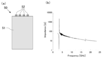
- FIG. 2A shows an Al electrode (wavelength 1.2 ⁇ m, thickness 0.08 wavelength) provided as a blind electrode (IDT) 52 on the surface of a 42 ° YX LT film 51 currently in practical use.
- the frequency characteristics of the SAW resonator 50 shown were determined. The result is shown in FIG. 2 (b).
- the frequency of the basic mode (0th order) was 3.2 GHz
- the band was 3.6%
- the impedance ratio was 65 dB.
- 17.2 GHz a small response that seems to be overtone of 5 times or more is observed, but it can be confirmed that it is not at a usable level.
- the blind electrode 12a is a Cu electrode having a wavelength of 1.2 ⁇ m and a thickness of 0.1 wavelength, and the piezoelectric substrate 11 has an oiler angle (90 °, 90 °, 35 °).
- LT thinness 0.2 wavelength
- the acoustic multilayer film 13 is a low acoustic impedance film 13a (thickness 0.25 wavelength) made of SiO 2 film and a high acoustic impedance film 13b (thickness 0.25 wavelength) made of Ta film.
- Wavelength was alternately laminated in a total of 6 layers, and the frequency characteristics when the support substrate 14 was a Si substrate were determined.
- FIG. 3 (a) The result is shown in FIG. 3 (a).
- the basic mode of SAW was confirmed at 3.8 GHz, and a large response of spurious and its harmonics was confirmed at 2 GHz, 5.1 GHz, 6.3 GHz, and 8.2 GHz.
- an overtone response of about 3 times that of the 0th-order mode was confirmed at 11 GHz.
- the 5.1 GHz response is an LLSAW with a sound velocity of 6,100 m / s.
- Euler angles ( ⁇ , ⁇ , ⁇ ) are simply represented by ( ⁇ , ⁇ , ⁇ ).
- the blind electrode 12a is a Cu electrode having a thickness of 0.1 wavelength
- the piezoelectric substrate 11 is a (90 °, 90 °, 42.5 °) LN (thickness).
- sandwiching the Al electrode of the floating electrode 12b is sandwiching the Al electrode of the floating electrode 12b (thickness 0.01 wavelength)
- the acoustic multilayer film 13 is composed of a SiO 2 film, a low acoustic impedance film 13a (thickness 0.05 wavelength), and Ta.
- the thickness of the Ta film of the high acoustic impedance film 13b is 0.23 from 0.05 wavelength when the high acoustic impedance film 13b made of the film is alternately laminated in a total of 6 layers and the support substrate 14 is a Si substrate. The frequency characteristics when the wavelength was changed were obtained. The result is shown in FIG. 3 (b).
- the characteristic near the center frequency of 3 GHz is the basic mode, and the characteristic near the center frequency is about three times the overtone (“O3” in the figure).
- the characteristic of 12 GHz is about 4 times overtone (“O4” in the figure)
- the characteristic near 15 GHz is about 5 times overtone (“O5” in the figure).
- a characteristic there is one characteristic (hereinafter referred to as A characteristic) between the overtone of about 3 times and the overtone of about 4 times. It was confirmed that when the thickness of the Ta film was 0.115 wavelength, the overtone frequency was reduced by about 3 times and the response was reduced.
- the overtone frequency which was about four times lower, was lowered at the same time, but the response remained small.
- the thickness of the Ta film is 0.13 wavelength
- the frequency of overtone which is about 4 times lower than that when the thickness of Ta film is 0.05 wavelength is further lowered, and the overtone is about 3 times (about 10 GHz), but it is large. It was confirmed that it had an impedance ratio.
- the frequency of each characteristic decreased, and the phenomenon in which the impedance ratio changed to a large or small value was repeated.
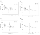
- the frequency characteristics of the elastic wave device 10 shown in FIGS. 1A and 1B when various conditions were changed were determined.
- the blind electrode 12a is a Cu electrode having a wavelength of 1.2 ⁇ m and a thickness of 0.1 wavelength
- the piezoelectric substrate 11 is (0 °, 85 °, 0 °) LN.
- the acoustic multilayer film 13 is composed of a low acoustic impedance film 13a (thickness 0.06 wavelength) made of an Al film and a high acoustic impedance film 13b (thickness 0.06 wavelength) made of a W film.
- FIG. 4 (a) shows the frequency characteristics when a total of 6 layers are alternately laminated and the support substrate 14 is a Si substrate.
- the weeping electrode 12a is a Cu electrode 12 having a wavelength of 1.2 ⁇ m and a thickness of 0.1 wavelength
- the piezoelectric substrate 11 is (90 °, 90 °, 42. 5 °) LN (thickness 0.2 wavelength)
- floating electrode 12b as Al electrode
- acoustic multilayer film 13 composed of low acoustic impedance film 13a (thickness 0.05 wavelength) made of SiO 2 film and Ta film.
- FIG. 4B shows the frequency characteristics when the high acoustic impedance film 13b (thickness 0.05 wavelength) is alternately laminated in a total of 6 layers and the support substrate 14 is a Si substrate.
- the blind electrode 12a is a Cu electrode having a wavelength of 1.2 ⁇ m and a thickness of 0.1 wavelength
- the piezoelectric substrate 11 is (0 °, 85 °, 0 °) LT.
- the acoustic multilayer film 13 is composed of a low acoustic impedance film 13a (thickness 0.05 wavelength) made of an Al film and a high acoustic impedance film 13b (thickness 0.05 wavelength) made of a W film.
- 4 (c) shows the frequency characteristics when a total of 6 layers are alternately laminated and the support substrate 14 is a Si substrate. Further, in the elastic wave device 10 shown in FIG.
- the blind electrode 12a is a Cu electrode having a wavelength of 1.2 ⁇ m and a thickness of 0.1 wavelength
- the piezoelectric substrate 11 is (90 °, 90 °, 35 °) LT.
- the floating electrode 12b is an Al electrode
- the acoustic multilayer film 13 is a low acoustic impedance film 13a (thickness 0.07 wavelength) made of a SiO 2 film and a high acoustic impedance film made of a Ta film.
- FIG. 4 (d) shows the frequency characteristics when a total of 6 layers of 13b (thickness 0.07 wavelength) are alternately laminated and the support substrate 14 is a Si substrate.
- the floating electrode 12b shown in FIG. 1A it is preferable that the surface of the Al film in contact with the piezoelectric substrate 11 is an insulating alumite film.
- the magnitude of the SAW basic mode and spurious at 1 to 5 GHz is much smaller than that of the basic mode of FIG. 3 in all frequency characteristics.
- the response of the overtone of 9 to 11 GHz was large, and a band of 3.2 to 8.1% and an impedance ratio of 71 to 76 dB could be obtained.
- the frequency of this overtone corresponds to a sound velocity of 12,000 to 13,000 m / s, which is 3.1 times the frequency of the basic mode shown in FIG.
- the following shows the results when various conditions are changed in order to obtain an overtone with good characteristics.
- the blind electrode 12a is a Cu electrode having a wavelength of 1.2 ⁇ m and a thickness of 0.1 wavelength
- the piezoelectric substrate 11 is a (0 °, ⁇ , 0 °) LN (thickness 0). .2 wavelengths)
- the acoustic multilayer film 13 is alternately composed of a low acoustic impedance film 13a (thickness 0.05 wavelength) made of an Al film and a high acoustic impedance film 13b (thickness 0.05 wavelength) made of a W film.
- the support substrate 14 is a Si substrate (hereinafter, Cu (0.1 ⁇ ) / (0 °, ⁇ , 0 °) LN (0.2 ⁇ ) / Al (0.05 ⁇ )).
- Bandlength when / W (0.05 ⁇ ) / Al (0.05 ⁇ ) / W (0.05 ⁇ ) / Al (0.05 ⁇ ) / W (0.05 ⁇ ) / Si substrate, etc.) The dependence of (Bandwidth) and impedance ratio on the Euler angle ⁇ is shown in FIGS. 5 (a) and 5 (b), respectively.
- the surface of the Al film of the first layer of the acoustic multilayer film 13 on the piezoelectric substrate side may be treated with insulating alumite, or an insulating low acoustic impedance film such as a SiO 2 film may be used. desirable.
- the surface of the Al film of the first layer of the following examples is assumed to be anodized. do.
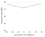
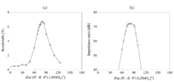
- the elastic wave device 10 shown in FIG. 1A is Cu (0.1 ⁇ ) / ( ⁇ , 85 °, 0 °) LN (0.2 ⁇ ) / Al (0.05 ⁇ ) / W (0.05 ⁇ ) /.
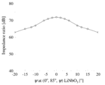
- the elastic wave device 10 shown in FIG. 1A is Cu (0.1 ⁇ ) / (0 °, 85 °, ⁇ ) LN (0.2 ⁇ ) / Al (0.05 ⁇ ) / W (0.05 ⁇ ) /.
- LN (-30 ° to 30 °, 60 ° to 103 °, -15 ° to 15 °) is used as the piezoelectric substrate 11.
- a band of 3% or more and an impedance ratio of 60 dB or more can be obtained.
- an impedance ratio of 65 dB or more can be obtained, and (-30 ° to 30 °, 78 ° to 92).
- °, -6 ° to 6 °) It can be seen that an impedance ratio of 70 dB or more can be obtained by using LN.
- the elastic wave device 10 shown in FIG. 1A is a Cu (0.1 ⁇ ) / (0 °, 85 °, 0 °) LN (0.2 ⁇ ) / Al film / W film / Al film / W film / Al.
- the dependence of the impedance ratio on the W film thickness when the film thickness of the W film of the high acoustic impedance film 13b is changed with the Al film thickness as 0.05 wavelength is determined. It is shown in FIG. 8 (a).
- FIG. 8B shows the dependence of the impedance ratio on the Al film thickness when the film thickness of the Al film of the low acoustic impedance film 13a is changed with the W film thickness as 0.05 wavelength.
- FIG. 8A shows an example when the Al film thickness is 0.05 wavelength, but even when the Al film thickness is 0.02 to 0.118 wavelength, the optimum W film thickness is the Al film thickness. Showed the same film thickness as when the wavelength was 0.05.
- a large impedance ratio can be obtained even when the Al film thickness of the low acoustic impedance film 13a is 0.2 wavelength or more, and when the Al film thickness is 0.216 to 0.275 wavelength, the impedance is 60 dB or more.
- the ratio is obtained and the Al film thickness is 0.22 to 0.27 wavelength, an impedance ratio of 65 dB or more is obtained, and when the Al film thickness is 0.225 to 0.254 wavelength, an impedance ratio of 70 dB or more is obtained. It was confirmed that it could be obtained.
- FIG. 8B shows an example when the W film thickness is 0.05 wavelength, but even when the W film thickness is 0.02 to 0.118 wavelength, the optimum Al film thickness is the W film thickness. Showed the same film thickness as when the wavelength was 0.05.
- the elastic wave device 10 shown in FIG. 1 (b) is Cu (0.1 ⁇ ) / (0 °, ⁇ , 0 °) LN (0.2 ⁇ ) / floating electrode / Al (0.05 ⁇ ) / W (0. 05 ⁇ ) / Al (0.05 ⁇ ) / W (0.05 ⁇ ) / Al (0.05 ⁇ ) / W (0.05 ⁇ ) / Si
- the dependence of the band and impedance ratio on Euler angles ⁇ for the substrate are shown in FIGS. 9 (a) and 9 (b), respectively.
- the surface of the first Al film of the acoustic multilayer film 13 is anodized with insulation. When an Al electrode that has not been anodized is used in the first layer, the Al film in the first layer may also be used as a floating electrode.
- the elastic wave device 10 shown in FIG. 1 (b) is Cu (0.1 ⁇ ) / (0 °, 85 °, 0 °) LN (0.2 ⁇ ) / floating electrode / Al film / W film / Al film / W.
- the sex is shown in FIG. 10 (a).
- FIG. 10B shows the dependence of the impedance ratio on the Al film thickness when the film thickness of the Al film of the low acoustic impedance film 13a is changed with the W film thickness as 0.05 wavelength.
- a large impedance ratio can be obtained even when the W film thickness of the high acoustic impedance film 13b is 0.2 wavelength or more, and when the W film thickness is 0.216 to 0.275 wavelength, the impedance is 60 dB or more.
- the ratio is obtained and the W film thickness is 0.22 to 0.27 wavelength, an impedance ratio of 65 dB or more is obtained, and when the W film thickness is 0.23 to 0.26 wavelength, an impedance ratio of 70 dB or more is obtained. It was confirmed that it could be obtained.
- FIG. 10A shows an example when the Al film thickness is 0.05 wavelength, but even when the Al film thickness is 0.02 to 0.113 wavelength, the optimum W film thickness is the Al film thickness. Showed the same film thickness as when the wavelength was 0.05.
- a large impedance ratio can be obtained even when the Al film thickness of the low acoustic impedance film 13a is 0.2 wavelength or more, and when the Al film thickness is 0.216 to 0.275 wavelength, the impedance is 60 dB or more.
- the ratio is obtained and the Al film thickness is 0.22 to 0.27 wavelength, an impedance ratio of 65 dB or more is obtained, and when the Al film thickness is 0.225 to 0.254 wavelength, an impedance ratio of 70 dB or more is obtained. It was confirmed that it could be obtained.
- FIG. 10B shows an example when the W film thickness is 0.05 wavelength, but even when the W film thickness is 0.02 to 0.105 wavelength, the optimum Al film thickness is the W film thickness. Showed the same film thickness as when the wavelength was 0.05.
- the elastic wave device 10 shown in FIG. 1A is Cu (0.1 ⁇ ) / (90 °, 90 °, ⁇ ) LN (0.2 ⁇ ) / Al (0.05 ⁇ ) / W (0.05 ⁇ ) /.
- the dependence of the band and impedance ratio on Euler angles ⁇ for Al (0.05 ⁇ ) / W (0.05 ⁇ ) / Al (0.05 ⁇ ) / W (0.05 ⁇ ) / Si substrates is shown in FIG. 11, respectively. It is shown in (a) and (b).
- Euler angles ⁇ and ⁇ are not shown, almost the same values are obtained at ⁇ 6 °, and 60 dB or more at (90 ° ⁇ 6 °, 90 ° ⁇ 6 °, -20 ° to 48 °).
- Impedance ratios of 65 dB or more were obtained at (90 ° ⁇ 6 °, 90 ° ⁇ 6 °, -10 ° to 43 °), and (90 ° ⁇ 6 °, 90 ° ⁇ 6 °,- It was confirmed that an impedance ratio of 70 dB or more can be obtained at (2 ° to 33 °).
- the elastic wave device 10 shown in FIG. 1A is a Cu (0.1 ⁇ ) / (90 °, 90 °, 42.5 °) LN (0.2 ⁇ ) / Al film / W film / Al film / W film.
- FIG. 12 (a) shows the dependence of the impedance ratio on the Al film thickness when the film thickness of the Al film of the low acoustic impedance film 13a is changed with the W film thickness as 0.05 wavelength.
- a large impedance ratio can be obtained even when the W film thickness of the high acoustic impedance film 13b is 0.2 wavelength or more, and when the W film thickness is 0.216 to 0.275 wavelength, the impedance is 60 dB or more.
- the ratio is obtained and the W film thickness is 0.22 to 0.27 wavelength, an impedance ratio of 65 dB or more is obtained, and when the W film thickness is 0.23 to 0.26 wavelength, an impedance ratio of 70 dB or more is obtained. It was confirmed that it could be obtained.
- FIG. 12A shows an example when the Al film thickness is 0.05 wavelength, but even when the Al film thickness is 0.014 to 0.113 wavelength, the optimum W film thickness is the Al film thickness. Showed the same film thickness as when the wavelength was 0.05.
- a large impedance ratio can be obtained even when the Al film thickness of the low acoustic impedance film 13a is 0.2 wavelength or more, and when the Al film thickness is 0.216 to 0.275 wavelength, the impedance is 60 dB or more.
- the ratio is obtained and the Al film thickness is 0.22 to 0.27 wavelength, an impedance ratio of 65 dB or more is obtained, and when the Al film thickness is 0.225 to 0.254 wavelength, an impedance ratio of 70 dB or more is obtained. It was confirmed that it could be obtained.
- FIG. 12B shows an example when the W film thickness is 0.05 wavelength, but even when the W film thickness is 0.015 to 0.104 wavelength, the optimum Al film thickness is the W film thickness. Showed the same film thickness as when the wavelength was 0.05.
- the elastic wave device 10 shown in FIG. 1 (b) is Cu (0.1 ⁇ ) / (90 °, 90 °, ⁇ ) LN (0.2 ⁇ ) / floating electrode / SiO 2 (0.05 ⁇ ) / Ta (0). .05 ⁇ ) / SiO 2 (0.05 ⁇ ) / Ta (0.05 ⁇ ) / SiO 2 (0.05 ⁇ ) / Ta (0.05 ⁇ ) / Si Dependence of band and impedance ratio on Euler angles ⁇
- the sexes are shown in FIGS. 13 (a) and 13 (b), respectively. As shown in FIGS.
- the elastic wave device 10 shown in FIG. 1 (b) is Cu (0.1 ⁇ ) / (90 °, 90 °, 42.5 °) LN (0.2 ⁇ ) / floating electrode / SiO 2 film / Ta film / SiO. 2 film / Ta film / SiO 2 film / Ta film / Si substrate, the impedance ratio when the film thickness of the Ta film of the high acoustic impedance film 13b is changed with the SiO 2 film thickness as 0.05 wavelength.
- FIG. 14 (a) shows the dependence of the impedance ratio on the SiO 2 film thickness when the film thickness of the SiO 2 film of the low acoustic impedance film 13a is changed with the Ta film thickness as 0.05 wavelength. ..
- FIG. 14A shows an example when the SiO 2 film thickness is 0.05 wavelength, but even when the SiO 2 film thickness is 0.012 to 0.096 wavelength, the optimum Ta film thickness is SiO. 2 The film thickness was the same as when the film thickness was 0.05 wavelength.
- the SiO 2 film thickness of the low acoustic impedance film 13a is 0.012 to 0.096 wavelength, 0.12 to 0.185 wavelength, and 0.216 to 0.275 wavelength.
- an impedance ratio of 60 dB or more can be obtained, and at the wavelengths of 0.015 to 0.092 wavelength, 0.125 to 0.18 wavelength, and 0.22 to 0.27 wavelength, an impedance ratio of 65 dB or more can be obtained.
- 0.02 to 0.087 wavelengths, 0.133 to 0.172 wavelengths, and 0.225 to 0.254 wavelengths have an impedance ratio of 70 dB or more, and 0.04 to 0.07 wavelengths have 75 dB. It was confirmed that the above impedance ratio can be obtained.
- FIG. 14B shows an example when the Ta film thickness is 0.05 wavelength, but even when the Ta film thickness is 0.015 to 0.1 wavelength, the optimum SiO 2 film thickness is the Ta film. The film thickness was the same as when the thickness was 0.05 wavelength.
- the elastic wave device 10 shown in FIG. 1A is Cu (0.1 ⁇ ) / (0 °, ⁇ , 0 °) LT (0.15 ⁇ ) / Al (0.05 ⁇ ) / W (0.05 ⁇ ) /.
- the dependence of the band and impedance ratio on Euler angles ⁇ for Al (0.05 ⁇ ) / W (0.05 ⁇ ) / Al (0.05 ⁇ ) / W (0.05 ⁇ ) / Si substrates is shown in FIG. 15, respectively. It is shown in (a) and (b). As shown in FIGS.
- An impedance ratio of 65 dB or more can be obtained with LT ( ⁇ 95 °, -15 ° to 15 °), and an impedance ratio of 70 dB or more can be obtained with LT (-30 ° to 30 °, 70 ° to 89 °, -6 ° to 6 °). Is obtained.
- the elastic wave device 10 shown in FIG. 1A is a Cu (0.1 ⁇ ) / (0 °, 85 °, 0 °) LT (0.15 ⁇ ) / Al film / W film / Al film / W film / Al.
- the dependence of the impedance ratio on the W film thickness when the film thickness of the W film of the high acoustic impedance film 13b is changed with the Al film thickness as 0.05 wavelength is determined. It is shown in FIG. 16 (a).
- FIG. 16B shows the dependence of the impedance ratio on the Al film thickness when the film thickness of the Al film of the low acoustic impedance film 13a is changed with the W film thickness as 0.05 wavelength.
- an impedance ratio of 60 dB or more is obtained and is 0.
- An impedance ratio of 65 dB or more is obtained at .025 to 0.095 wavelength and 0.117 to 0.19 wavelength, and 70 dB or more at 0.03 to 0.092 wavelength and 0.12 to 0.17 wavelength. It was confirmed that the impedance ratio of Although not shown, a large impedance ratio can be obtained even when the W film thickness of the high acoustic impedance film 13b is 0.2 wavelength or more, and when the W film thickness is 0.216 to 0.275 wavelength, the impedance is 60 dB or more.
- FIG. 16A shows an example when the Al film thickness is 0.05 wavelength, the optimum W film thickness is the Al film thickness even when the Al film thickness is 0.02 to 0.1 wavelength. Showed the same film thickness as when the wavelength was 0.05.
- FIG. 16B shows an example when the W film thickness is 0.05 wavelength, the optimum Al film thickness is the W film thickness even when the W film thickness is 0.02 to 0.1 wavelength. Showed the same film thickness as when the wavelength was 0.05.
- the elastic wave device 10 shown in FIG. 1 (b) is Cu (0.1 ⁇ ) / (0 °, ⁇ , 0 °) LT (0.15 ⁇ ) / floating electrode / Al (0.05 ⁇ ) / W (0. 05 ⁇ ) / Al (0.05 ⁇ ) / W (0.05 ⁇ ) / Al (0.05 ⁇ ) / W (0.05 ⁇ ) / Si substrate and Cu (0.1 ⁇ ) / (0 °, ⁇ , 0 °) LT (0.15 ⁇ ) / floating electrode / SiO 2 (0.05 ⁇ ) / Ta (0.05 ⁇ ) / SiO 2 (0.05 ⁇ ) / Ta (0.05 ⁇ ) / SiO 2 (0.05 ⁇ ) ) / Ta (0.05 ⁇ ) / Si substrate, the dependence of the band and the impedance ratio on the oiler angle ⁇ is shown in FIGS.
- the elastic wave device 10 shown in FIG. 1 (b) is Cu (0.1 ⁇ ) / (0 °, 85 °, 0 °) LT (0.15 ⁇ ) / floating electrode / Al film / W film / Al film / W.
- the sex is shown in FIG. 18 (a).
- FIG. 18B shows the dependence of the impedance ratio on the Al film thickness when the film thickness of the Al film of the low acoustic impedance film 13a is changed with the W film thickness as 0.05 wavelength.
- FIG. 18A shows an example when the Al film thickness is 0.05 wavelength, but even when the Al film thickness is 0.023 to 0.098 wavelength, the optimum W film thickness is the Al film thickness. Showed the same film thickness as when the wavelength was 0.05.
- FIG. 18B shows an example when the W film thickness is 0.05 wavelength, but even when the W film thickness is 0.023 to 0.097 wavelength, the optimum Al film thickness is the W film thickness. Showed the same film thickness as when the wavelength was 0.05.
- the elastic wave device 10 shown in FIG. 1A is Cu (0.1 ⁇ ) / (90 °, 90 °, ⁇ ) LT (0.15 ⁇ ) / Al (0.05 ⁇ ) / W (0.05 ⁇ ) /.
- the dependence of the band and impedance ratio on Euler angles ⁇ for Al (0.05 ⁇ ) / W (0.05 ⁇ ) / Al (0.05 ⁇ ) / W (0.05 ⁇ ) / Si substrates is shown in FIG. It is shown in (a) and (b). As shown in FIGS.
- An impedance ratio of 70 dB or more can be obtained at ⁇ 6 °, 90 ° ⁇ 6 °, 85 ° to 91 °), and 75 dB or more at (90 ° ⁇ 6 °, 90 ° ⁇ 6 °, 23 ° to 83 °). It was confirmed that the impedance ratio can be obtained.
- the elastic wave device 10 shown in FIG. 1A is a Cu (0.1 ⁇ ) / (90 °, 90 °, 35 °) LT (0.15 ⁇ ) / Al film / W film / Al film / W film / Al.
- the dependence of the impedance ratio on the W film thickness when the film thickness of the W film of the high acoustic impedance film 13b is changed with the Al film thickness as 0.05 wavelength is determined. It is shown in FIG. 20 (a).
- FIG. 20B shows the dependence of the impedance ratio on the Al film thickness when the film thickness of the Al film of the low acoustic impedance film 13a is changed with the W film thickness as 0.05 wavelength.
- a large impedance ratio can be obtained even when the W film thickness of the high acoustic impedance film 13b is 0.2 wavelength or more, and when the W film thickness is 0.216 to 0.275 wavelength, the impedance is 60 dB or more.
- the ratio is obtained and the W film thickness is 0.22 to 0.27 wavelength, an impedance ratio of 65 dB or more is obtained, and when the W film thickness is 0.225 to 0.26 wavelength, an impedance ratio of 70 dB or more is obtained. It was confirmed that it could be obtained.
- FIG. 20A shows an example when the Al film thickness is 0.05 wavelength, but even when the Al film thickness is 0.018 to 0.08 wavelength, the optimum W film thickness is the Al film thickness. Showed the same film thickness as when the wavelength was 0.05.
- a large impedance ratio can be obtained even when the Al film thickness of the high acoustic impedance film 13b is 0.2 wavelength or more, and when the Al film thickness is 0.216 to 0.275 wavelength, the impedance is 60 dB or more.
- the ratio is obtained and the Al film thickness is 0.22 to 0.27 wavelength, an impedance ratio of 65 dB or more is obtained, and when the Al film thickness is 0.225 to 0.26 wavelength, an impedance ratio of 70 dB or more is obtained. It was confirmed that it could be obtained.
- FIG. 20B shows an example when the W film thickness is 0.05 wavelength, but even when the W film thickness is 0.016 to 0.08 wavelength, the optimum Al film thickness is the W film thickness. Showed the same film thickness as when the wavelength was 0.05.
- the elastic wave device 10 shown in FIG. 1 (b) is Cu (0.1 ⁇ ) / (90 °, 90 °, ⁇ ) LT (0.15 ⁇ ) / floating electrode / SiO 2 (0.05 ⁇ ) / Ta (0). .05 ⁇ ) / SiO 2 (0.05 ⁇ ) / Ta (0.05 ⁇ ) / SiO 2 (0.05 ⁇ ) / Ta (0.05 ⁇ ) / Si Dependence of band and impedance ratio on Euler angles ⁇
- the sexes are shown in FIGS. 21 (a) and 21 (b), respectively. As shown in FIGS.
- the elastic wave device 10 shown in FIG. 1B is a Cu (0.1 ⁇ ) / (90 °, 90 °, 35 °) LT (0.15 ⁇ ) / floating electrode / SiO 2 film / Ta film / SiO 2 film. / Ta film / SiO 2 film / Ta film / Si substrate, Ta film of impedance ratio when the film thickness of Ta film of high acoustic impedance film 13b is changed with SiO 2 film thickness as 0.05 wavelength.
- the dependence on the film thickness is shown in FIG. 22 (a). Further, FIG. 22B shows the dependence of the impedance ratio on the SiO 2 film thickness when the film thickness of the SiO 2 film of the low acoustic impedance film 13a is changed with the Ta film thickness as 0.05 wavelength. ..
- FIG. 22A shows an example when the SiO 2 film thickness is 0.05 wavelength, but even when the SiO 2 film thickness is 0.015 to 0.085 wavelength, the optimum Ta film thickness is SiO. 2 The film thickness was the same as when the film thickness was 0.05 wavelength.
- the SiO 2 film thickness of the low acoustic impedance film 13a is 0.015 to 0.085 wavelength, 0.118 to 0.18 wavelength, and 0.216 to 0.275 wavelength.
- an impedance ratio of 60 dB or more is obtained, and at 0.017 to 0.093 wavelength, 0.122 to 0.175 wavelength, and 0.22 to 0.27 wavelength, an impedance ratio of 65 dB or more is obtained.
- 0.02 to 0.087 wavelength, 0.13 to 0.17 wavelength, and 0.225 to 0.26 wavelength an impedance ratio of 70 dB or more is obtained, and 0.035 to 0.08 wavelength. It was confirmed that an impedance ratio of 75 dB or more could be obtained.
- FIG. 20B shows an example when the Ta film thickness is 0.05 wavelength, but even when the Ta film thickness is 0.015 to 0.085 wavelength, the optimum SiO 2 film thickness is the Ta film. The film thickness was the same as when the thickness was 0.05 wavelength.
- the elastic wave device 10 shown in FIG. 1 (b) is Cu (0.1 ⁇ ) / (90 °, 90 °, 42.5 °) LN (0.2 ⁇ ) / floating electrode / SiO 2 film (0.05 ⁇ ).
- FIG. 23 shows the dependence of the impedance ratio on the thickness of the piezoelectric substrate 11 in the case of 05 ⁇ ) / Ta film (0.05 ⁇ ) / SiO 2 film (0.05 ⁇ ) / Ta film (0.05 ⁇ ) / Si substrate. Shown in. As shown in FIG. 23, when the thicknesses of LN and LT are 5 wavelengths or less and 2.4 wavelengths or less, an impedance ratio of 65 dB or more is obtained, and the thicknesses of LN and LT are 1.2 wavelengths or less and 1 wavelength, respectively.
- an impedance ratio of 70 dB or more can be obtained, and when the thicknesses of LN and LT are 0.3 to 0.02 wavelength and 0.25 to 0.02 wavelength, respectively, an impedance ratio of 75 dB or more can be obtained. confirmed.
- the elastic wave device 10 shown in FIG. 1 (b) is Cu (0.1 ⁇ ) / (90 °, 90 °, 35 °) LT (0.15 ⁇ ) / floating electrode / SiO 2 film (0.05 ⁇ ) / Ta.
- the dependence of the acoustic multilayer film 13 on the number of layers is shown in FIG. As shown in FIG.
- the film such as Ti provided to increase the adhesive strength has a film thickness of several tens of nm to several hundreds of nm, and the acoustic multilayer film 13 has a thickness of several tens of nm to several hundreds of nm. Since it is relatively thin compared to each film, it is not included as an acoustic impedance film.
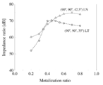
- the elastic wave device 10 shown in FIG. 1B is a blind electrode 12a / (90 °, 90 °, 35 °) LT (0.15 ⁇ ) / floating electrode / SiO 2 film (0.05 ⁇ ) / Ta film ( 0.05 ⁇ ) / SiO 2 film (0.05 ⁇ ) / Ta film (0.05 ⁇ ) / SiO 2 film (0.05 ⁇ ) / Ta film (0.05 ⁇ ) / Si substrate (0.05 ⁇ ) / Si substrate
- FIG. 25 the metallization ratio (MR) of the blind electrode 12a is set to 0.5, and the results when a Cu electrode, an Al electrode, an Au electrode, and a Mo electrode are used as the blind electrode 12a are shown.
- the electrode thickness when the electrode thickness is 0.01 to 0.045 wavelength and 0.1 to 0.21 wavelength, an impedance ratio of 65 dB or more can be obtained, and the electrode thickness is 0.02 to 0.041 wavelength and It was confirmed that an impedance ratio of 70 dB or more was obtained when the wavelength was 0.135 to 0.197, and an impedance ratio of 75 dB or more was obtained when the electrode thickness was 0.159 to 0.182 wavelength.
- the electrode thickness is 0.005 to 0.02 wavelength and 0.062 to 0.165 wavelength
- an impedance ratio of 65 dB or more can be obtained, and the electrode thickness is 0.01 to 0.0152 wavelength and It was confirmed that an impedance ratio of 70 dB or more was obtained when the wavelength was 0.064 to 0.155, and an impedance ratio of 75 dB or more was obtained when the electrode thickness was 0.08 to 0.12 wavelength.
- the electrode thickness when the electrode thickness is 0.008 to 0.03 wavelength and 0.055 to 0.19 wavelength, an impedance ratio of 65 dB or more can be obtained, and the electrode thickness is 0.0125 to 0.027 wavelength and It was confirmed that an impedance ratio of 70 dB or more was obtained when the wavelength was 0.065 to 0.165, and an impedance ratio of 75 dB or more was obtained when the electrode thickness was 0.095 to 0.13 wavelength.
- interdigital electrodes 12a when the density is less than 1800 kg / m 3 or more 6000 kg / m 3, the same electrode thickness and the Al electrode becomes optimum thickness, when less than 6000 kg / m 3 or more 10000 kg / m 3, and the Cu electrode
- the same electrode thickness is the optimum thickness, and when it is 10000 kg / m 3 or more and less than 15000 kg / m 3 , the same electrode thickness as the Mo electrode is the optimum thickness, and when it is 15000 kg / m 3 or more and less than 25000 kg / m 3 , the same electrode as the Au electrode.
- the thickness is the optimum thickness.
- the optimum thickness is determined by converting with the average density thereof.
- the metallization ratio (MR) of the blind electrode 12a deviates from 0.5
- the optimum thickness is H ⁇ 0.5 / MR, where H is the optimum thickness when the MR is 0.5.
- the elastic wave device 10 shown in FIG. 1 (b) is Cu (0.1 ⁇ ) / (90 °, 90 °, 42.5 °) LN (0.2 ⁇ ) / floating electrode / SiO 2 film (0.05 ⁇ ).
- FIG. 26 The dependence of the impedance ratio on the MR of the weeping electrode 12a in the case of 05 ⁇ ) / Ta film (0.05 ⁇ ) / SiO 2 film (0.05 ⁇ ) / Ta film (0.05 ⁇ ) / Si substrate is shown in FIG. 26. Shown in. As shown in FIG. 26, it was confirmed that an impedance ratio of 65 dB or more can be obtained when the MR is 0.35 to 0.8 for both LN and LT. Further, it was confirmed that in LN, an impedance ratio of 70 dB or more was obtained when MR was 045 to 0.8, and in LT, an impedance ratio of 68 dB or more was obtained when MR was 0.45 to 0.6. Was done.
- the elastic wave device 10 shown in FIG. 1A is a Cu (0.1 ⁇ ) / (90 °, 90 °, 42.5 °) LN (0.2 ⁇ ) / acoustic multilayer film [Multi acoustic layers; SiO]. 2 (0.05 ⁇ ) / Ta (0.05 ⁇ ) / SiO 2 (0.05 ⁇ ) / Ta (0.05 ⁇ ) / SiO 2 (0.05 ⁇ ) / Ta (0.05 ⁇ ) / SiO 2 (0.05 ⁇ ) ) / Ta (0.05 ⁇ )] / Si substrate, the displacement distribution of the frequency characteristic of the overtone near the sound velocity of 11,000 m / s is shown in FIG. 27 (b). As shown in FIG.
- the mutation distribution was SAW containing the SH component as a main component.
- the elastic wave device of Patent Document 3 and the elastic wave device 10 of the embodiment of the present invention have a completely different displacement distribution in addition to the difference in frequency and sound velocity, the difference in the basic mode of LLSAW and the overtone of SAW. From the different, it is clear that the vibration modes are also different.
Landscapes
- Physics & Mathematics (AREA)
- Acoustics & Sound (AREA)
- Chemical & Material Sciences (AREA)
- Engineering & Computer Science (AREA)
- Materials Engineering (AREA)
- Surface Acoustic Wave Elements And Circuit Networks Thereof (AREA)
Priority Applications (3)
| Application Number | Priority Date | Filing Date | Title |
|---|---|---|---|
| CN202180017384.6A CN115176416A (zh) | 2020-02-28 | 2021-02-12 | 弹性波器件 |
| JP2022503254A JPWO2021172032A1 (https=) | 2020-02-28 | 2021-02-12 | |
| US17/801,886 US12334900B2 (en) | 2020-02-28 | 2021-02-12 | Acoustic wave device |
Applications Claiming Priority (2)
| Application Number | Priority Date | Filing Date | Title |
|---|---|---|---|
| JP2020-034101 | 2020-02-28 | ||
| JP2020034101 | 2020-02-28 |
Publications (1)
| Publication Number | Publication Date |
|---|---|
| WO2021172032A1 true WO2021172032A1 (ja) | 2021-09-02 |
Family
ID=77491467
Family Applications (1)
| Application Number | Title | Priority Date | Filing Date |
|---|---|---|---|
| PCT/JP2021/005129 Ceased WO2021172032A1 (ja) | 2020-02-28 | 2021-02-12 | 弾性波デバイス |
Country Status (4)
| Country | Link |
|---|---|
| US (1) | US12334900B2 (https=) |
| JP (1) | JPWO2021172032A1 (https=) |
| CN (1) | CN115176416A (https=) |
| WO (1) | WO2021172032A1 (https=) |
Cited By (4)
| Publication number | Priority date | Publication date | Assignee | Title |
|---|---|---|---|---|
| JPWO2023085210A1 (https=) * | 2021-11-09 | 2023-05-19 | ||
| JP2023137104A (ja) * | 2022-03-17 | 2023-09-29 | 太陽誘電株式会社 | 弾性波デバイス、フィルタ、およびマルチプレクサ |
| WO2025052739A1 (ja) * | 2023-09-06 | 2025-03-13 | 国立大学法人東北大学 | 弾性波デバイス |
| WO2026070989A1 (ja) * | 2024-09-25 | 2026-04-02 | 株式会社村田製作所 | 弾性波装置 |
Families Citing this family (1)
| Publication number | Priority date | Publication date | Assignee | Title |
|---|---|---|---|---|
| JP7527604B2 (ja) * | 2019-08-08 | 2024-08-05 | 国立大学法人東北大学 | 弾性波デバイス |
Citations (7)
| Publication number | Priority date | Publication date | Assignee | Title |
|---|---|---|---|---|
| JPH11220352A (ja) * | 1998-02-03 | 1999-08-10 | Seiko Epson Corp | 3次オーバートーンsaw共振子 |
| JP2011015397A (ja) * | 2009-06-30 | 2011-01-20 | Commissariat A L'energie Atomique Et Aux Energies Alternatives | 導波型音響波共振装置およびその装置の製造方法 |
| WO2012086441A1 (ja) * | 2010-12-24 | 2012-06-28 | 株式会社村田製作所 | 弾性波装置及びその製造方法 |
| JP2013528996A (ja) * | 2010-04-23 | 2013-07-11 | テクノロジアン テュトキムスケスクス ヴェーテーテー | 広帯域音響結合薄膜bawフィルタ |
| JP2015537492A (ja) * | 2012-12-12 | 2015-12-24 | エプコス アクチエンゲゼルシャフトEpcos Ag | 電子音響部品 |
| WO2016047255A1 (ja) * | 2014-09-26 | 2016-03-31 | 国立大学法人東北大学 | 弾性波装置 |
| WO2020204045A1 (ja) * | 2019-04-03 | 2020-10-08 | 国立大学法人東北大学 | 高次モード弾性表面波デバイス |
Family Cites Families (12)
| Publication number | Priority date | Publication date | Assignee | Title |
|---|---|---|---|---|
| JP3204290B2 (ja) * | 1995-02-09 | 2001-09-04 | 住友電気工業株式会社 | 表面弾性波素子 |
| CN102217194A (zh) * | 2008-11-18 | 2011-10-12 | 株式会社村田制作所 | 可调滤波器 |
| JP5354020B2 (ja) * | 2009-10-13 | 2013-11-27 | 株式会社村田製作所 | 弾性表面波装置 |
| CN106209007B (zh) * | 2010-12-24 | 2019-07-05 | 株式会社村田制作所 | 弹性波装置 |
| JP5592811B2 (ja) * | 2011-01-27 | 2014-09-17 | 日東電工株式会社 | 半導体装置の製造方法 |
| CN103733642B (zh) * | 2011-08-12 | 2016-12-14 | 株式会社特瑞君思半导体 | 驱动电路 |
| US10938367B2 (en) * | 2016-03-31 | 2021-03-02 | Qorvo Us, Inc. | Solidly mounted layer thin film device with grounding layer |
| US11258427B2 (en) * | 2016-11-25 | 2022-02-22 | Tohoku University | Acoustic wave devices |
| JP2018182615A (ja) | 2017-04-18 | 2018-11-15 | 株式会社村田製作所 | 弾性波装置 |
| CN108039872A (zh) * | 2017-12-26 | 2018-05-15 | 海宁市瑞宏科技有限公司 | 一种用于高性能声表面波滤波器的谐振器结构设计 |
| JP2019140456A (ja) * | 2018-02-07 | 2019-08-22 | 株式会社村田製作所 | 弾性波装置、高周波フロントエンド回路及び通信装置 |
| US11223341B2 (en) * | 2019-10-22 | 2022-01-11 | Vtt Technical Research Centre Of Finland Ltd | Suppressing parasitic sidebands in lateral bulk acoustic wave resonators |
-
2021
- 2021-02-12 WO PCT/JP2021/005129 patent/WO2021172032A1/ja not_active Ceased
- 2021-02-12 CN CN202180017384.6A patent/CN115176416A/zh active Pending
- 2021-02-12 US US17/801,886 patent/US12334900B2/en active Active
- 2021-02-12 JP JP2022503254A patent/JPWO2021172032A1/ja active Pending
Patent Citations (7)
| Publication number | Priority date | Publication date | Assignee | Title |
|---|---|---|---|---|
| JPH11220352A (ja) * | 1998-02-03 | 1999-08-10 | Seiko Epson Corp | 3次オーバートーンsaw共振子 |
| JP2011015397A (ja) * | 2009-06-30 | 2011-01-20 | Commissariat A L'energie Atomique Et Aux Energies Alternatives | 導波型音響波共振装置およびその装置の製造方法 |
| JP2013528996A (ja) * | 2010-04-23 | 2013-07-11 | テクノロジアン テュトキムスケスクス ヴェーテーテー | 広帯域音響結合薄膜bawフィルタ |
| WO2012086441A1 (ja) * | 2010-12-24 | 2012-06-28 | 株式会社村田製作所 | 弾性波装置及びその製造方法 |
| JP2015537492A (ja) * | 2012-12-12 | 2015-12-24 | エプコス アクチエンゲゼルシャフトEpcos Ag | 電子音響部品 |
| WO2016047255A1 (ja) * | 2014-09-26 | 2016-03-31 | 国立大学法人東北大学 | 弾性波装置 |
| WO2020204045A1 (ja) * | 2019-04-03 | 2020-10-08 | 国立大学法人東北大学 | 高次モード弾性表面波デバイス |
Cited By (5)
| Publication number | Priority date | Publication date | Assignee | Title |
|---|---|---|---|---|
| JPWO2023085210A1 (https=) * | 2021-11-09 | 2023-05-19 | ||
| JP2023137104A (ja) * | 2022-03-17 | 2023-09-29 | 太陽誘電株式会社 | 弾性波デバイス、フィルタ、およびマルチプレクサ |
| JP7829370B2 (ja) | 2022-03-17 | 2026-03-13 | 太陽誘電株式会社 | 弾性波デバイス、フィルタ、およびマルチプレクサ |
| WO2025052739A1 (ja) * | 2023-09-06 | 2025-03-13 | 国立大学法人東北大学 | 弾性波デバイス |
| WO2026070989A1 (ja) * | 2024-09-25 | 2026-04-02 | 株式会社村田製作所 | 弾性波装置 |
Also Published As
| Publication number | Publication date |
|---|---|
| US20230361752A1 (en) | 2023-11-09 |
| CN115176416A (zh) | 2022-10-11 |
| US12334900B2 (en) | 2025-06-17 |
| JPWO2021172032A1 (https=) | 2021-09-02 |
Similar Documents
| Publication | Publication Date | Title |
|---|---|---|
| JP7808882B2 (ja) | 高次モードの弾性表面波を利用するデバイスを製造する方法 | |
| WO2021172032A1 (ja) | 弾性波デバイス | |
| US9276558B2 (en) | Surface acoustic wave device including a confinement layer | |
| JP5910763B2 (ja) | 弾性波装置 | |
| KR100681692B1 (ko) | 탄성 표면파 장치 및 그 제조방법 | |
| CN110120794B (zh) | 弹性波装置、高频前端电路以及通信装置 | |
| JP4337816B2 (ja) | 弾性境界波装置 | |
| JP4483785B2 (ja) | 弾性境界波装置 | |
| WO2006114930A1 (ja) | 弾性境界波装置 | |
| JP7497750B2 (ja) | 弾性波装置 | |
| CN101789769A (zh) | 弹性波装置 | |
| JPWO2005086345A1 (ja) | 弾性境界波装置 | |
| KR102722448B1 (ko) | 탄성파 장치 | |
| JP2023060058A (ja) | 弾性波共振器、フィルタおよびマルチプレクサ | |
| CN114070257B (zh) | 声波装置、滤波器及多路复用器 | |
| WO2010116783A1 (ja) | 弾性波装置 | |
| JP7378723B2 (ja) | 弾性波デバイス | |
| JP7587766B2 (ja) | 共振子 | |
| JP7527604B2 (ja) | 弾性波デバイス | |
| TWI894342B (zh) | 彈性波裝置 | |
| JP7575023B2 (ja) | 弾性表面波デバイス | |
| JP2001077654A (ja) | 表面弾性波素子 | |
| HK40064695A (en) | High-order mode surface acoustic wave device |
Legal Events
| Date | Code | Title | Description |
|---|---|---|---|
| 121 | Ep: the epo has been informed by wipo that ep was designated in this application |
Ref document number: 21759650 Country of ref document: EP Kind code of ref document: A1 |
|
| ENP | Entry into the national phase |
Ref document number: 2022503254 Country of ref document: JP Kind code of ref document: A |
|
| NENP | Non-entry into the national phase |
Ref country code: DE |
|
| 122 | Ep: pct application non-entry in european phase |
Ref document number: 21759650 Country of ref document: EP Kind code of ref document: A1 |
|
| WWG | Wipo information: grant in national office |
Ref document number: 17801886 Country of ref document: US |