WO2021157431A1 - 発光デバイス - Google Patents
発光デバイス Download PDFInfo
- Publication number
- WO2021157431A1 WO2021157431A1 PCT/JP2021/002636 JP2021002636W WO2021157431A1 WO 2021157431 A1 WO2021157431 A1 WO 2021157431A1 JP 2021002636 W JP2021002636 W JP 2021002636W WO 2021157431 A1 WO2021157431 A1 WO 2021157431A1
- Authority
- WO
- WIPO (PCT)
- Prior art keywords
- layer
- light
- emitting device
- light emitting
- contact layer
- Prior art date
- Legal status (The legal status is an assumption and is not a legal conclusion. Google has not performed a legal analysis and makes no representation as to the accuracy of the status listed.)
- Ceased
Links
Images



Classifications
-
- H—ELECTRICITY
- H01—ELECTRIC ELEMENTS
- H01S—DEVICES USING THE PROCESS OF LIGHT AMPLIFICATION BY STIMULATED EMISSION OF RADIATION [LASER] TO AMPLIFY OR GENERATE LIGHT; DEVICES USING STIMULATED EMISSION OF ELECTROMAGNETIC RADIATION IN WAVE RANGES OTHER THAN OPTICAL
- H01S5/00—Semiconductor lasers
- H01S5/10—Construction or shape of the optical resonator, e.g. extended or external cavity, coupled cavities, bent-guide, varying width, thickness or composition of the active region
- H01S5/18—Surface-emitting [SE] lasers, e.g. having both horizontal and vertical cavities
- H01S5/183—Surface-emitting [SE] lasers, e.g. having both horizontal and vertical cavities having only vertical cavities, e.g. vertical cavity surface-emitting lasers [VCSEL]
- H01S5/18305—Surface-emitting [SE] lasers, e.g. having both horizontal and vertical cavities having only vertical cavities, e.g. vertical cavity surface-emitting lasers [VCSEL] with emission through the substrate, i.e. bottom emission
-
- H—ELECTRICITY
- H01—ELECTRIC ELEMENTS
- H01S—DEVICES USING THE PROCESS OF LIGHT AMPLIFICATION BY STIMULATED EMISSION OF RADIATION [LASER] TO AMPLIFY OR GENERATE LIGHT; DEVICES USING STIMULATED EMISSION OF ELECTROMAGNETIC RADIATION IN WAVE RANGES OTHER THAN OPTICAL
- H01S5/00—Semiconductor lasers
- H01S5/10—Construction or shape of the optical resonator, e.g. extended or external cavity, coupled cavities, bent-guide, varying width, thickness or composition of the active region
- H01S5/18—Surface-emitting [SE] lasers, e.g. having both horizontal and vertical cavities
- H01S5/183—Surface-emitting [SE] lasers, e.g. having both horizontal and vertical cavities having only vertical cavities, e.g. vertical cavity surface-emitting lasers [VCSEL]
- H01S5/18308—Surface-emitting [SE] lasers, e.g. having both horizontal and vertical cavities having only vertical cavities, e.g. vertical cavity surface-emitting lasers [VCSEL] having a special structure for lateral current or light confinement
-
- G—PHYSICS
- G01—MEASURING; TESTING
- G01S—RADIO DIRECTION-FINDING; RADIO NAVIGATION; DETERMINING DISTANCE OR VELOCITY BY USE OF RADIO WAVES; LOCATING OR PRESENCE-DETECTING BY USE OF THE REFLECTION OR RERADIATION OF RADIO WAVES; ANALOGOUS ARRANGEMENTS USING OTHER WAVES
- G01S17/00—Systems using the reflection or reradiation of electromagnetic waves other than radio waves, e.g. lidar systems
- G01S17/88—Lidar systems specially adapted for specific applications
- G01S17/89—Lidar systems specially adapted for specific applications for mapping or imaging
- G01S17/894—Three-dimensional [3D] imaging with simultaneous measurement of time-of-flight at a two-dimensional [2D] array of receiver pixels, e.g. time-of-flight cameras or flash lidar
-
- G—PHYSICS
- G01—MEASURING; TESTING
- G01S—RADIO DIRECTION-FINDING; RADIO NAVIGATION; DETERMINING DISTANCE OR VELOCITY BY USE OF RADIO WAVES; LOCATING OR PRESENCE-DETECTING BY USE OF THE REFLECTION OR RERADIATION OF RADIO WAVES; ANALOGOUS ARRANGEMENTS USING OTHER WAVES
- G01S7/00—Details of systems according to groups G01S13/00, G01S15/00, G01S17/00
- G01S7/48—Details of systems according to groups G01S13/00, G01S15/00, G01S17/00 of systems according to group G01S17/00
- G01S7/481—Constructional features, e.g. arrangements of optical elements
- G01S7/4814—Constructional features, e.g. arrangements of optical elements of transmitters alone
-
- H—ELECTRICITY
- H01—ELECTRIC ELEMENTS
- H01S—DEVICES USING THE PROCESS OF LIGHT AMPLIFICATION BY STIMULATED EMISSION OF RADIATION [LASER] TO AMPLIFY OR GENERATE LIGHT; DEVICES USING STIMULATED EMISSION OF ELECTROMAGNETIC RADIATION IN WAVE RANGES OTHER THAN OPTICAL
- H01S5/00—Semiconductor lasers
- H01S5/04—Processes or apparatus for excitation, e.g. pumping, e.g. by electron beams
- H01S5/042—Electrical excitation ; Circuits therefor
- H01S5/0425—Electrodes, e.g. characterised by the structure
- H01S5/04256—Electrodes, e.g. characterised by the structure characterised by the configuration
-
- H—ELECTRICITY
- H01—ELECTRIC ELEMENTS
- H01S—DEVICES USING THE PROCESS OF LIGHT AMPLIFICATION BY STIMULATED EMISSION OF RADIATION [LASER] TO AMPLIFY OR GENERATE LIGHT; DEVICES USING STIMULATED EMISSION OF ELECTROMAGNETIC RADIATION IN WAVE RANGES OTHER THAN OPTICAL
- H01S5/00—Semiconductor lasers
- H01S5/40—Arrangement of two or more semiconductor lasers, not provided for in groups H01S5/02 - H01S5/30
- H01S5/42—Arrays of surface emitting lasers
- H01S5/423—Arrays of surface emitting lasers having a vertical cavity
-
- G—PHYSICS
- G01—MEASURING; TESTING
- G01S—RADIO DIRECTION-FINDING; RADIO NAVIGATION; DETERMINING DISTANCE OR VELOCITY BY USE OF RADIO WAVES; LOCATING OR PRESENCE-DETECTING BY USE OF THE REFLECTION OR RERADIATION OF RADIO WAVES; ANALOGOUS ARRANGEMENTS USING OTHER WAVES
- G01S17/00—Systems using the reflection or reradiation of electromagnetic waves other than radio waves, e.g. lidar systems
- G01S17/02—Systems using the reflection of electromagnetic waves other than radio waves
- G01S17/06—Systems determining position data of a target
- G01S17/08—Systems determining position data of a target for measuring distance only
- G01S17/32—Systems determining position data of a target for measuring distance only using transmission of continuous waves, whether amplitude-, frequency-, or phase-modulated, or unmodulated
- G01S17/36—Systems determining position data of a target for measuring distance only using transmission of continuous waves, whether amplitude-, frequency-, or phase-modulated, or unmodulated with phase comparison between the received signal and the contemporaneously transmitted signal
-
- H—ELECTRICITY
- H01—ELECTRIC ELEMENTS
- H01S—DEVICES USING THE PROCESS OF LIGHT AMPLIFICATION BY STIMULATED EMISSION OF RADIATION [LASER] TO AMPLIFY OR GENERATE LIGHT; DEVICES USING STIMULATED EMISSION OF ELECTROMAGNETIC RADIATION IN WAVE RANGES OTHER THAN OPTICAL
- H01S2301/00—Functional characteristics
- H01S2301/17—Semiconductor lasers comprising special layers
- H01S2301/173—The laser chip comprising special buffer layers, e.g. dislocation prevention or reduction
-
- H—ELECTRICITY
- H01—ELECTRIC ELEMENTS
- H01S—DEVICES USING THE PROCESS OF LIGHT AMPLIFICATION BY STIMULATED EMISSION OF RADIATION [LASER] TO AMPLIFY OR GENERATE LIGHT; DEVICES USING STIMULATED EMISSION OF ELECTROMAGNETIC RADIATION IN WAVE RANGES OTHER THAN OPTICAL
- H01S5/00—Semiconductor lasers
- H01S5/02—Structural details or components not essential to laser action
- H01S5/0206—Substrates, e.g. growth, shape, material, removal or bonding
- H01S5/0208—Semi-insulating substrates
-
- H—ELECTRICITY
- H01—ELECTRIC ELEMENTS
- H01S—DEVICES USING THE PROCESS OF LIGHT AMPLIFICATION BY STIMULATED EMISSION OF RADIATION [LASER] TO AMPLIFY OR GENERATE LIGHT; DEVICES USING STIMULATED EMISSION OF ELECTROMAGNETIC RADIATION IN WAVE RANGES OTHER THAN OPTICAL
- H01S5/00—Semiconductor lasers
- H01S5/04—Processes or apparatus for excitation, e.g. pumping, e.g. by electron beams
- H01S5/042—Electrical excitation ; Circuits therefor
- H01S5/0425—Electrodes, e.g. characterised by the structure
- H01S5/04256—Electrodes, e.g. characterised by the structure characterised by the configuration
- H01S5/04257—Electrodes, e.g. characterised by the structure characterised by the configuration having positive and negative electrodes on the same side of the substrate
-
- H—ELECTRICITY
- H01—ELECTRIC ELEMENTS
- H01S—DEVICES USING THE PROCESS OF LIGHT AMPLIFICATION BY STIMULATED EMISSION OF RADIATION [LASER] TO AMPLIFY OR GENERATE LIGHT; DEVICES USING STIMULATED EMISSION OF ELECTROMAGNETIC RADIATION IN WAVE RANGES OTHER THAN OPTICAL
- H01S5/00—Semiconductor lasers
- H01S5/10—Construction or shape of the optical resonator, e.g. extended or external cavity, coupled cavities, bent-guide, varying width, thickness or composition of the active region
- H01S5/18—Surface-emitting [SE] lasers, e.g. having both horizontal and vertical cavities
- H01S5/183—Surface-emitting [SE] lasers, e.g. having both horizontal and vertical cavities having only vertical cavities, e.g. vertical cavity surface-emitting lasers [VCSEL]
- H01S5/18308—Surface-emitting [SE] lasers, e.g. having both horizontal and vertical cavities having only vertical cavities, e.g. vertical cavity surface-emitting lasers [VCSEL] having a special structure for lateral current or light confinement
- H01S5/18311—Surface-emitting [SE] lasers, e.g. having both horizontal and vertical cavities having only vertical cavities, e.g. vertical cavity surface-emitting lasers [VCSEL] having a special structure for lateral current or light confinement using selective oxidation
-
- H—ELECTRICITY
- H01—ELECTRIC ELEMENTS
- H01S—DEVICES USING THE PROCESS OF LIGHT AMPLIFICATION BY STIMULATED EMISSION OF RADIATION [LASER] TO AMPLIFY OR GENERATE LIGHT; DEVICES USING STIMULATED EMISSION OF ELECTROMAGNETIC RADIATION IN WAVE RANGES OTHER THAN OPTICAL
- H01S5/00—Semiconductor lasers
- H01S5/10—Construction or shape of the optical resonator, e.g. extended or external cavity, coupled cavities, bent-guide, varying width, thickness or composition of the active region
- H01S5/18—Surface-emitting [SE] lasers, e.g. having both horizontal and vertical cavities
- H01S5/183—Surface-emitting [SE] lasers, e.g. having both horizontal and vertical cavities having only vertical cavities, e.g. vertical cavity surface-emitting lasers [VCSEL]
- H01S5/18344—Surface-emitting [SE] lasers, e.g. having both horizontal and vertical cavities having only vertical cavities, e.g. vertical cavity surface-emitting lasers [VCSEL] characterized by the mesa, e.g. dimensions or shape of the mesa
- H01S5/18347—Mesa comprising active layer
-
- H—ELECTRICITY
- H01—ELECTRIC ELEMENTS
- H01S—DEVICES USING THE PROCESS OF LIGHT AMPLIFICATION BY STIMULATED EMISSION OF RADIATION [LASER] TO AMPLIFY OR GENERATE LIGHT; DEVICES USING STIMULATED EMISSION OF ELECTROMAGNETIC RADIATION IN WAVE RANGES OTHER THAN OPTICAL
- H01S5/00—Semiconductor lasers
- H01S5/30—Structure or shape of the active region; Materials used for the active region
- H01S5/34—Structure or shape of the active region; Materials used for the active region comprising quantum well or superlattice structures, e.g. single quantum well [SQW] lasers, multiple quantum well [MQW] lasers or graded index separate confinement heterostructure [GRINSCH] lasers
- H01S5/343—Structure or shape of the active region; Materials used for the active region comprising quantum well or superlattice structures, e.g. single quantum well [SQW] lasers, multiple quantum well [MQW] lasers or graded index separate confinement heterostructure [GRINSCH] lasers in AIIIBV compounds, e.g. AlGaAs-laser, InP-based laser
- H01S5/34313—Structure or shape of the active region; Materials used for the active region comprising quantum well or superlattice structures, e.g. single quantum well [SQW] lasers, multiple quantum well [MQW] lasers or graded index separate confinement heterostructure [GRINSCH] lasers in AIIIBV compounds, e.g. AlGaAs-laser, InP-based laser with a well layer having only As as V-compound, e.g. AlGaAs, InGaAs
Definitions
- the present disclosure relates to, for example, a back-emission type light emitting device.
- Patent Document 1 includes an n-type semiconductor multilayer film constituting a substrate-side mirror, a substrate-side contact / injection layer, a p-type semiconductor multilayer film, and a light-emitting layer on an n-type or semi-insulating GaAs substrate.
- a planar light emitting device in which a cavity and an n-type semiconductor multilayer film constituting an air-side mirror are formed in this order is disclosed.
- the light emitting device of the embodiment of the present disclosure includes a substrate having a first surface and a second surface facing each other, a first contact layer laminated on the first surface of the substrate, and a first contact layer.
- a buffer layer having at least one of a carrier concentration, a material composition, and a composition ratio different from that of the first contact layer, and the first contact layer and the buffer layer are laminated on the first surface of the substrate. It is provided with a semiconductor laminate having a light emitting region capable of emitting laser light.
- a buffer layer having at least one of the carrier concentration, the material composition, and the composition ratio different from that of the first contact layer is provided between the first contact layer and the semiconductor laminate. I did. As a result, a semiconductor laminate having excellent crystal quality is formed.
- FIG. 3 is a block diagram showing an example of a schematic configuration of a distance measuring device using the lighting device provided with the semiconductor laser shown in FIG. 1.
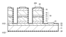
- FIG. 1 schematically shows an example of a cross-sectional configuration of a light emitting device (semiconductor laser 1) according to an embodiment of the present disclosure.
- the semiconductor laser 1 is, for example, a back-emission type VCSEL (Vertical Cavity Surface Emitting LASER), for example, a plurality of VCSELs are integrated in an array as a plurality of light emitting regions.
- VCSEL Vertical Cavity Surface Emitting LASER
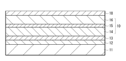
- the semiconductor laser 1 has, for example, a plurality of semiconductor laminates 10 on the first surface (surface (surface 11S1)) of the substrate 11.
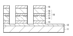
- the semiconductor laminate 10 has, for example, a columnar shape (mesa shape), and for example, the first light reflecting layer 14, the active layer 15, and the second light reflecting layer 16 are laminated in this order.
- a current constriction layer 17 forming a current injection region 17A is provided between the first light reflection layer 14 and the active layer 15.
- the semiconductor laminate 10 corresponds to a specific example of the "semiconductor laminate" of the present disclosure.
- the first contact layer 12 and the buffer layer 13 are laminated in this order between the semiconductor laminate 10 and the substrate 11, and the buffer layer 13 forms a mesa shape together with the semiconductor laminate 10.
- the first contact layer 12 extends on the substrate 11 as a common layer for the plurality of semiconductor laminates 10.
- a first electrode 21 is provided on the first contact layer 12 as a common electrode for each semiconductor laminate 10.
- a second contact layer 18 and a second electrode 22 are formed on the upper surface (surface 10S1) of each semiconductor laminate 10 in this order, respectively.
- the upper surface (surface 12S1) of the first contact layer 12 excluding the first electrode 21 and the second electrode 22, the upper surface of the second contact layer 18, and the side surfaces of the second contact layer 18, the semiconductor laminate 10 and the buffer layer 13 It is covered with the insulating film 23, and the second surface (back surface (surface 11S2)) of the substrate 11 is covered with the insulating film 24.
- the substrate 11 is a support substrate on which a plurality of semiconductor laminates 10 are integrated.
- the substrate 11 is composed of, for example, a semi-insulating substrate made of a GaAs-based semiconductor that does not contain impurities. Further, the substrate 11 may be any as long as it has a low carrier concentration and the absorption of laser light is reduced, and is not necessarily limited to a general semi-insulating substrate.
- a substrate having a p-type or n-type carrier concentration of 5 ⁇ 10 17 cm -3 or less can be used as the substrate 11.
- the first contact layer 12 is made of, for example, a GaAs-based semiconductor having conductivity.
- the first contact layer 12 is for electrically connecting the first electrode 21 and the first light reflecting layer 14 of each semiconductor laminate 10.
- the first contact layer 12 is composed of a p-type GaAs having a high carrier concentration, for example, a carrier concentration of 1 ⁇ 10 19 cm -3 or more.
- the first contact layer 12 corresponds to a specific example of the “first contact layer” of the present disclosure.
- the film thickness of the first contact layer in the stacking direction is, for example, 200 nm or more and 1500 nm or less.
- the buffer layer 13 is for recovering the crystal quality of the semiconductor laminate 10 formed above the first contact layer 12.
- the buffer layer 13 preferably has the following configuration.
- the buffer layer 13 is formed with a carrier concentration different from that of the first contact layer 12.
- the buffer layer 13 has a lower carrier concentration than the first contact layer 12, for example, a carrier concentration of less than 1 ⁇ 10 19 cm -3 , preferably 5 ⁇ 10 18 cm -3 or less. It is composed of p-type GaAs that it has.
- the buffer layer 13 is configured by using a semiconductor having a material composition and a composition ratio different from that of the first contact layer 12 (for example, the GaAs layer).
- the buffer layer 13 can be formed as a single-layer film or a laminated film including a layer made of any of the above semiconductor materials.
- the buffer layer 13 is formed above the first contact layer 12 by adopting at least one of the above configurations to alleviate the deterioration of the crystallinity of the first contact layer 12 due to high-concentration doping. The crystal quality of the semiconductor laminate 10 is restored.
- the film thickness of the buffer layer 13 in the stacking direction is, for example, 100 nm or more and 1000 nm or less.
- the first light reflecting layer 14 is arranged between the buffer layer 13 and the current constriction layer 17, and faces the second light reflection layer 16 with the active layer 15 and the current constriction layer 17 in between.
- the first light reflecting layer 14 resonates the light generated in the active layer 15 with the second light reflecting layer 16.
- the first light reflecting layer 14 corresponds to a specific example of the "first light reflecting layer" of the present disclosure.
- the first light reflecting layer 14 is a DBR (Distributed Bragg Reflector) layer in which low refractive index layers (not shown) and high refractive index layers (not shown) are alternately laminated.
- the low refractive index layer is composed of, for example, a p-type Al x1 Ga 1-x1 As (0 ⁇ x1 ⁇ 1) having an optical film thickness of ⁇ ⁇ 1 / 4n
- the high refractive index layer is, for example, an optical film thickness of ⁇ ⁇ . It is composed of 1 / 4n p-type Al x2 Ga 1-x2 As (0 ⁇ x2 ⁇ x1).
- ⁇ is the oscillation wavelength of the laser beam emitted from each light emitting region
- n is the refractive index.
- the active layer 15 is provided between the first light reflecting layer 14 and the second light reflecting layer 16.
- the active layer 15 is made of, for example, an aluminum gallium arsenide (AlGaAs) -based semiconductor material.
- AlGaAs aluminum gallium arsenide
- holes and electrons injected from the first electrode 21 and the second electrode 22 are luminescent and recombinated to generate stimulated emission light.
- the region of the active layer 15 facing the current injection region 17A is the light emitting region.
- undoped Al x3 Ga 1-x3 As (0 ⁇ x3 ⁇ 0.45) can be used.
- the active layer 15 may have, for example, a Multi Quantum Well (MQW) structure of GaAs and AlGaAs.
- MQW Multi Quantum Well
- the constituent material of the active layer 15 may be selected according to the desired wavelength region of the laser beam. For example, in the case of obtaining laser characteristics in the 900 nm band, a multiple quantum well structure of indium gallium arsenic (InGaAs) and AlGaAs is used.
- the active layer 15 may be formed.
- the active layer 15 corresponds to a specific example of the “active layer” of the present disclosure.
- the second light reflecting layer 16 is a DBR layer arranged between the active layer 15 and the second contact layer 18.
- the second light reflecting layer 16 faces the first light reflecting layer 14 with the active layer 15 and the current constriction layer 17 in between.
- the second light reflecting layer 16 corresponds to a specific example of the "second light reflecting layer" of the present disclosure.
- the second light reflecting layer 16 has a laminated structure in which low refractive index layers and high refractive index layers are alternately laminated.
- the low refractive index layer is, for example, an n-type Al x4 Ga 1-x4 As (0 ⁇ x4 ⁇ 1) having an optical film thickness of ⁇ / 4n.
- the high refractive index layer is, for example, an n-type Al x5 Ga 1-x5 As (0 ⁇ x5 ⁇ x4) having an optical film thickness of ⁇ / 4n.
- the current constriction layer 17 is provided between the first light reflection layer 14 and the active layer 15, and is formed in an annular shape having a predetermined width from the outer peripheral side to the inner side of the semiconductor laminate 10 having a mesa shape, for example. ing.
- the current constriction layer 17 is provided between the first light reflection layer 14 and the active layer 15, and has an opening having a predetermined width in the central portion thereof, and this opening becomes the current injection region 17A.
- the current constriction layer 17 is made of, for example, p-type AlGaAs.
- the current constriction layer 17 is composed of Al 0.85 Ga 0.15 As to Al As, and by oxidizing this to form an aluminum oxide (AlO x ) layer, the current is constricted.
- AlO x aluminum oxide
- the semiconductor laser 1 by providing the current constriction layer 17, the current to be injected from the first electrode 21 into the active layer 15 is constricted, and the current injection efficiency is improved.
- the second contact layer 18 is made of, for example, a GaAs-based semiconductor having conductivity.
- the second contact layer 18 is made of, for example, an n-type GaAs.
- the second contact layer 18 corresponds to a specific example of the "second contact layer" of the present disclosure.
- the first electrode 21 is provided on the first contact layer 12, and is formed of, for example, a multilayer film of titanium (Ti) / platinum (Pt) / gold (Au).
- the second electrode 22 is provided above the semiconductor laminate 10, specifically, on the second contact layer 18, and is, for example, a gold-germanium (Au-Ge) / nickel (Ni) / gold (Au) multilayer film. Is formed by.
- the insulating film 23 is formed continuously, for example, on the upper surface of the second contact layer 18, the second contact layer 18, the side surfaces of the semiconductor laminate 10 and the buffer layer 13, and the upper surface (surface 12S1) of the first contact layer 12. There is.
- the insulating film 23 is made of a single-layer film or a laminated film such as silicon nitride (SiN) or silicon oxide (SiO 2).
- An opening 23H (see, for example, FIG. 2D) is provided at a predetermined position on the upper surface of each of the second contact layers 18 and the first contact layer 12 of the insulating film 23, and the first electrode 21 is provided in each opening 23H.
- the second electrode 22 is embedded.
- the insulating film 24 is formed on the back surface (surface 11S2) of the substrate 11, for example, the entire surface.
- the insulating film 24 is made of a single-layer film or a laminated film such as silicon nitride (SiN) or silicon oxide (SiO 2).
- the plurality of semiconductor laminates 10 provided on the substrate 11 and the first electrode 21 are electrically connected to each other by, for example, a first contact layer 12 formed of p-type GaAs. It is a semiconductor laser having a so-called common anode structure connected to.
- the semiconductor laser 1 when a predetermined voltage is applied to the first electrode 21 and the second electrode 22, a voltage is applied to the semiconductor laminate 10 from the first electrode 21 and the second electrode 22. As a result, electrons are injected from the first electrode 21 and holes are injected into the active layer 15 from the second electrode 22, and light is generated by recombination of the electrons and holes. The light resonates and is amplified between the first light reflecting layer 14 and the second light reflecting layer 16, and the laser beam L is emitted from the back surface (surface 11S2) of the substrate 11.
- the first contact layer 12, the buffer layer 13, and the first contact layer 12 are formed on the substrate 11 by an epitaxial crystal growth method such as a metal organic chemical vapor deposition (MOCVD) method.
- MOCVD metal organic chemical vapor deposition
- Each compound semiconductor layer constituting the light reflecting layer 14, the active layer 15, the second light reflecting layer 16 and the second contact layer 18 is formed in this order to prepare an epibuffer.
- a methyl-based organometallic compound such as trimethylaluminum (TMAl), trimethylgallium (TMGa), or trimethylindium (TMIn) and arsine (AsH 3 ) gas are used as a raw material for donor impurities.
- TMAl trimethylaluminum
- TMGa trimethylgallium
- TMIn trimethylindium
- AsH 3 arsine
- Uses, for example, disilane (Si 2 H 6 ) and uses, for example, carbon tetrabromide (CBr 4 ) as a raw material
- the second contact layer 18 and the second contact layer 18 are used as a mask.
- the light reflecting layer 16, the active layer 15, and the first light reflecting layer 14 are etched to form a columnar mesa structure (semiconductor laminate 10).
- RIE reactive Ion Etching
- Cl-based gas Cl-based gas
- an oxide layer having a high aluminum (Al) composition for example, an AlGaAs layer, which has been laminated in advance during epi-growth, is oxidized and a current is narrowed (current narrowing layer 17).
- Al aluminum
- the buffer layer 13 is removed by etching to expose the first contact layer 12.
- the insulating film 24 is formed.
- the first electrode 21 and the second electrode 22 are formed on the first contact layer 12 and the second contact layer 18, respectively.
- the insulating films 23 and 24 are formed by, for example, a chemical vapor deposition (CVD) method or an atomic layer deposition (ALD) method.
- the insulating film 23 is formed so as to cover the entire upper surface (surface 12S1) of the first contact layer 12 exposed by etching from the upper surface of the second contact layer 18, and then a resist film (surface 12S1) having a predetermined pattern is formed on the insulating film 23. (Not shown) is formed into a pattern, and etching such as RIE is performed to form an opening 23H at a predetermined position. Then, for example, a lift-off method using a resist pattern is used to form a pattern of the first electrode 21 and the second electrode 22 on the first contact layer 12 and on the upper surface of the second contact layer 18, respectively. As a result, the semiconductor laser 1 shown in FIG. 1 is completed.
- a buffer layer 13 having a carrier concentration, a material composition, or a composition ratio different from that of the first contact layer 12 is provided between the first contact layer 12 and the semiconductor laminate 10. I did. As a result, the semiconductor laminate 10 having excellent crystal quality is formed. This will be described below.
- a contact layer is provided in the middle of the DBR layer like the above-mentioned planar light emitting element, and a light emitting layer (active layer) is provided via an electrode provided on the contact layer. ) Is applied with a voltage. Therefore, the contact layer is generally formed with a high carrier concentration.
- the contact layer having a high carrier concentration is formed at a position close to the active layer in the DBR layer as described above, the light absorption by the contact layer may be increased and the laser oscillation characteristics may be deteriorated.
- the film thickness of the contact layer is reduced in order to reduce the light absorption of the contact layer, there is a possibility that the margin at the time of process processing is lost and the manufacturing yield is lowered. Further, since the crystallinity of the contact layer doped with a high concentration of impurities tends to deteriorate, the crystallinity of the device structure growing on the contact layer may decrease.
- a buffer layer 13 having a carrier concentration, a material composition, or a composition ratio different from that of the first contact layer 12 is provided on the first contact layer 12, and the buffer layer 13 is provided.
- the first light reflecting layer 14, the active layer 15, and the second light reflecting layer 16 constituting the device structure (semiconductor laminate 10) are crystal-grown through the structure. This alleviates the deterioration of the crystallinity of the first contact layer 12, and makes it possible to form the semiconductor laminate 10 in which the crystal quality is maintained.
- any of the carrier concentration, the material composition, and the composition ratio between the first contact layer 12 and the semiconductor laminate 10 is different from that of the first contact layer 12. Since the buffer layer 13 is provided, it is possible to maintain the crystal quality of the semiconductor laminate 10 formed above the first contact layer (for example, on the buffer layer 13). Therefore, it is possible to improve the reliability.
- the buffer layer 13 is provided between the first contact layer 12 and the semiconductor laminate 10, the degree of freedom in designing the film thickness of the first contact layer is improved. As a result, it becomes possible to reduce the light absorption in the first contact layer while suppressing the decrease in the process margin. Therefore, it is possible to improve the oscillation characteristics of the laser beam L emitted from the back surface (surface 11S2) of the substrate 11 while maintaining the manufacturing yield.
- This technology can be applied to various electronic devices including semiconductor lasers.
- a light source provided in a portable electronic device such as a smartphone, a light source of various sensing devices for detecting a shape, an operation, or the like.
- FIG. 3 is a block diagram showing a schematic configuration of a distance measuring device (distance measuring device 200) using the lighting device 100 provided with the semiconductor laser 1 described above.
- the distance measuring device 200 measures the distance by the ToF method.
- the distance measuring device 200 includes, for example, a lighting device 100, a light receiving unit 210, a control unit 220, and a distance measuring unit 230.
- the lighting device 100 includes, for example, the semiconductor laser 1 shown in FIG. 1 or the like as a light source.
- illumination light is generated in synchronization with the emission control signal CLKp of a square wave.
- the light emission control signal CLKp is not limited to a rectangular wave as long as it is a periodic signal.
- the light emission control signal CLKp may be a sine wave.
- the light receiving unit 210 receives the reflected light reflected from the irradiation target object 300, and detects the amount of light received within the period of the vertical synchronization signal VSYNC each time the period of the vertical synchronization signal VSYNC has elapsed.
- a 60 Hz (Hz) periodic signal is used as the vertical sync signal VSYNC.
- a plurality of pixel circuits are arranged in a two-dimensional lattice pattern in the light receiving unit 210.
- the light receiving unit 210 supplies image data (frames) corresponding to the amount of light received by these pixel circuits to the distance measuring unit 230.
- the frequency of the vertical synchronization signal VSYNC is not limited to 60 hertz (Hz), and may be 30 hertz (Hz) or 120 hertz (Hz).
- the control unit 220 controls the lighting device 100.
- the control unit 220 generates a light emission control signal CLKp and supplies it to the lighting device 100 and the light receiving unit 210.
- the frequency of the light emission control signal CLKp is, for example, 20 MHz (MHz).
- the frequency of the light emission control signal CLKp is not limited to 20 MHz (MHz), and may be, for example, 5 MHz (MHz).
- the distance measuring unit 230 measures the distance to the irradiation target 300 by the ToF method based on the image data.
- the distance measuring unit 230 measures the distance for each pixel circuit and generates a depth map showing the distance to the object for each pixel as a gradation value. This depth map is used, for example, for image processing that performs a degree of blurring processing according to a distance, autofocus (AF) processing that obtains the in-focus of a focus lens according to a distance, and the like.
- AF autofocus
- the present technology has been described above with reference to embodiments and application examples, the present technology is not limited to the above-described embodiments and can be modified in various ways.
- the layer structure of the semiconductor laser 1 described in the above embodiment is an example, and other layers may be further provided.
- the material of each layer is also an example, and is not limited to the above-mentioned ones.
- the present technology can be configured as follows. According to the present technology having the following configuration, a buffer layer having at least one of the carrier concentration, the material composition, and the composition ratio different from that of the first contact layer 12 is provided between the first contact layer and the semiconductor laminate. Therefore, a semiconductor laminate having excellent crystal quality can be formed. Therefore, it is possible to improve the reliability.
- a light emitting device comprising a semiconductor laminate having a light emitting region capable of emitting laser light, which is laminated on the first surface of the substrate with the first contact layer and the buffer layer in between.
- the buffer layer has a single-layer structure or a laminated structure including at least one of a GaAs layer, an AlAs layer, an AlGaAs layer, an InGaAs layer, an AlGaInAs layer, a GaInP layer and an AlGaInP layer (1) to (3).
- the light emitting device according to any one of the above.
- the substrate is a semi-insulating substrate having a p-type or n-type carrier concentration of 5 ⁇ 10 17 cm -3 or less.
- the semiconductor laminate is any one of (1) to (5) above, wherein the first light-reflecting layer, the active layer, and the second light-reflecting layer are laminated in order from the substrate side.
- the semiconductor laminate further has a current constriction layer having a current injection region between the first light reflection layer and the active layer.
- the light emitting device according to any one of (6) to (8) above, wherein the semiconductor laminate is a light emitting device in which a second contact layer is further laminated on the second light reflecting layer.
- a plurality of the semiconductor laminates are provided on the first surface of the substrate.
- the light emitting device according to any one of (1) to (9), wherein the first contact layer is formed as a common layer for a plurality of the semiconductor laminates.
- (11) A first electrode provided on the surface of the semiconductor laminate opposite to the substrate and provided so that a predetermined voltage can be applied to the semiconductor laminate in the light emitting region, and the first contact.
- the light emitting device according to (10) above, further comprising a second electrode provided on the layer.
- (12) The light emitting device according to any one of (1) to (11), wherein the laser beam is emitted from the second surface of the substrate.
Landscapes
- Physics & Mathematics (AREA)
- General Physics & Mathematics (AREA)
- Electromagnetism (AREA)
- Condensed Matter Physics & Semiconductors (AREA)
- Optics & Photonics (AREA)
- Engineering & Computer Science (AREA)
- Computer Networks & Wireless Communication (AREA)
- Radar, Positioning & Navigation (AREA)
- Remote Sensing (AREA)
- Semiconductor Lasers (AREA)
Priority Applications (4)
| Application Number | Priority Date | Filing Date | Title |
|---|---|---|---|
| US17/792,238 US20230047126A1 (en) | 2020-02-07 | 2021-01-26 | Light emitting device |
| CN202180010791.4A CN115244804A (zh) | 2020-02-07 | 2021-01-26 | 发光器件 |
| JP2021575742A JPWO2021157431A1 (https=) | 2020-02-07 | 2021-01-26 | |
| EP21750147.7A EP4084242B1 (en) | 2020-02-07 | 2021-01-26 | Light-emitting device |
Applications Claiming Priority (2)
| Application Number | Priority Date | Filing Date | Title |
|---|---|---|---|
| JP2020-019567 | 2020-02-07 | ||
| JP2020019567 | 2020-02-07 |
Publications (1)
| Publication Number | Publication Date |
|---|---|
| WO2021157431A1 true WO2021157431A1 (ja) | 2021-08-12 |
Family
ID=77200041
Family Applications (1)
| Application Number | Title | Priority Date | Filing Date |
|---|---|---|---|
| PCT/JP2021/002636 Ceased WO2021157431A1 (ja) | 2020-02-07 | 2021-01-26 | 発光デバイス |
Country Status (6)
| Country | Link |
|---|---|
| US (1) | US20230047126A1 (https=) |
| EP (1) | EP4084242B1 (https=) |
| JP (1) | JPWO2021157431A1 (https=) |
| CN (1) | CN115244804A (https=) |
| TW (1) | TWI887340B (https=) |
| WO (1) | WO2021157431A1 (https=) |
Families Citing this family (1)
| Publication number | Priority date | Publication date | Assignee | Title |
|---|---|---|---|---|
| TWI844953B (zh) * | 2022-09-15 | 2024-06-11 | 台亞半導體股份有限公司 | 多層熱導反射鏡的面射型雷射 |
Citations (12)
| Publication number | Priority date | Publication date | Assignee | Title |
|---|---|---|---|---|
| JPH05211346A (ja) | 1991-01-21 | 1993-08-20 | Nippon Telegr & Teleph Corp <Ntt> | 面形発光素子 |
| US5625202A (en) * | 1995-06-08 | 1997-04-29 | University Of Central Florida | Modified wurtzite structure oxide compounds as substrates for III-V nitride compound semiconductor epitaxial thin film growth |
| JPH11214750A (ja) * | 1998-01-27 | 1999-08-06 | Sanyo Electric Co Ltd | 窒化ガリウム系化合物半導体発光素子の製造方法 |
| JPH11330554A (ja) * | 1998-03-12 | 1999-11-30 | Nichia Chem Ind Ltd | 窒化物半導体素子 |
| JP2000151025A (ja) * | 1998-11-10 | 2000-05-30 | Hitachi Ltd | 光システム |
| JP2004095838A (ja) * | 2002-08-30 | 2004-03-25 | Fuji Photo Film Co Ltd | 半導体レーザ素子 |
| JP2005243900A (ja) * | 2004-02-26 | 2005-09-08 | Sony Corp | 半導体発光素子およびその駆動方法 |
| JP2010016172A (ja) * | 2008-07-03 | 2010-01-21 | Seiko Epson Corp | 発光装置 |
| JP2013527484A (ja) * | 2009-12-19 | 2013-06-27 | トリルミナ コーポレーション | デジタル出力用レーザアレイを組み合わせるためのシステムおよび方法 |
| JP2015041627A (ja) * | 2013-08-20 | 2015-03-02 | ウシオ電機株式会社 | 半導体レーザ装置 |
| JP2019033210A (ja) * | 2017-08-09 | 2019-02-28 | 住友電気工業株式会社 | 面発光レーザ |
| JP2020019567A (ja) | 2018-07-04 | 2020-02-06 | 東洋製罐株式会社 | 充填システムおよび充填方法 |
Family Cites Families (16)
| Publication number | Priority date | Publication date | Assignee | Title |
|---|---|---|---|---|
| US5656832A (en) * | 1994-03-09 | 1997-08-12 | Kabushiki Kaisha Toshiba | Semiconductor heterojunction device with ALN buffer layer of 3nm-10nm average film thickness |
| KR100224881B1 (ko) * | 1996-07-25 | 1999-10-15 | 윤종용 | 표면광 레이저 |
| JP4018177B2 (ja) * | 1996-09-06 | 2007-12-05 | 株式会社東芝 | 窒化ガリウム系化合物半導体発光素子 |
| JP3684778B2 (ja) * | 1997-08-21 | 2005-08-17 | 富士ゼロックス株式会社 | 面発光型半導体レーザアレイ |
| KR100589621B1 (ko) * | 1998-03-12 | 2006-06-19 | 니치아 카가쿠 고교 가부시키가이샤 | 질화물 반도체 소자 |
| JP2001223384A (ja) * | 2000-02-08 | 2001-08-17 | Toshiba Corp | 半導体発光素子 |
| JP4250603B2 (ja) * | 2005-03-28 | 2009-04-08 | キヤノン株式会社 | テラヘルツ波の発生素子、及びその製造方法 |
| JP2006294811A (ja) * | 2005-04-08 | 2006-10-26 | Fuji Xerox Co Ltd | トンネル接合型面発光半導体レーザ素子およびその製造方法 |
| JP5653625B2 (ja) * | 2009-01-08 | 2015-01-14 | 古河電気工業株式会社 | 半導体発光素子およびその製造方法 |
| JP2011155087A (ja) * | 2010-01-26 | 2011-08-11 | Sony Corp | 面発光型半導体レーザおよびその製造方法 |
| US9640944B2 (en) * | 2015-09-08 | 2017-05-02 | Fuji Xerox Co., Ltd. | Method of manufacturing optical semiconductor element |
| JP6245319B1 (ja) * | 2016-06-30 | 2017-12-13 | 富士ゼロックス株式会社 | 発光部品、プリントヘッド、画像形成装置及び半導体積層基板 |
| US10116115B2 (en) * | 2017-02-22 | 2018-10-30 | Geoff W. Taylor | Integrated circuit implementing a VCSEL array or VCSEL device |
| US11309686B2 (en) * | 2017-06-20 | 2022-04-19 | Sony Corporation | Surface emitting laser and method of manufacturing the same |
| US10681474B2 (en) * | 2017-09-19 | 2020-06-09 | Vocalzoom Systems Ltd. | Laser-based devices utilizing improved self-mix sensing |
| EP4020724A4 (en) * | 2019-11-06 | 2023-09-13 | Sony Semiconductor Solutions Corporation | SURFACE EMITTING LASER DEVICE |
-
2021
- 2021-01-26 US US17/792,238 patent/US20230047126A1/en active Pending
- 2021-01-26 JP JP2021575742A patent/JPWO2021157431A1/ja active Pending
- 2021-01-26 EP EP21750147.7A patent/EP4084242B1/en active Active
- 2021-01-26 CN CN202180010791.4A patent/CN115244804A/zh active Pending
- 2021-01-26 WO PCT/JP2021/002636 patent/WO2021157431A1/ja not_active Ceased
- 2021-01-29 TW TW110103374A patent/TWI887340B/zh active
Patent Citations (12)
| Publication number | Priority date | Publication date | Assignee | Title |
|---|---|---|---|---|
| JPH05211346A (ja) | 1991-01-21 | 1993-08-20 | Nippon Telegr & Teleph Corp <Ntt> | 面形発光素子 |
| US5625202A (en) * | 1995-06-08 | 1997-04-29 | University Of Central Florida | Modified wurtzite structure oxide compounds as substrates for III-V nitride compound semiconductor epitaxial thin film growth |
| JPH11214750A (ja) * | 1998-01-27 | 1999-08-06 | Sanyo Electric Co Ltd | 窒化ガリウム系化合物半導体発光素子の製造方法 |
| JPH11330554A (ja) * | 1998-03-12 | 1999-11-30 | Nichia Chem Ind Ltd | 窒化物半導体素子 |
| JP2000151025A (ja) * | 1998-11-10 | 2000-05-30 | Hitachi Ltd | 光システム |
| JP2004095838A (ja) * | 2002-08-30 | 2004-03-25 | Fuji Photo Film Co Ltd | 半導体レーザ素子 |
| JP2005243900A (ja) * | 2004-02-26 | 2005-09-08 | Sony Corp | 半導体発光素子およびその駆動方法 |
| JP2010016172A (ja) * | 2008-07-03 | 2010-01-21 | Seiko Epson Corp | 発光装置 |
| JP2013527484A (ja) * | 2009-12-19 | 2013-06-27 | トリルミナ コーポレーション | デジタル出力用レーザアレイを組み合わせるためのシステムおよび方法 |
| JP2015041627A (ja) * | 2013-08-20 | 2015-03-02 | ウシオ電機株式会社 | 半導体レーザ装置 |
| JP2019033210A (ja) * | 2017-08-09 | 2019-02-28 | 住友電気工業株式会社 | 面発光レーザ |
| JP2020019567A (ja) | 2018-07-04 | 2020-02-06 | 東洋製罐株式会社 | 充填システムおよび充填方法 |
Non-Patent Citations (1)
| Title |
|---|
| See also references of EP4084242A4 |
Also Published As
| Publication number | Publication date |
|---|---|
| TW202137580A (zh) | 2021-10-01 |
| US20230047126A1 (en) | 2023-02-16 |
| TWI887340B (zh) | 2025-06-21 |
| EP4084242B1 (en) | 2024-12-18 |
| EP4084242A4 (en) | 2023-01-25 |
| CN115244804A (zh) | 2022-10-25 |
| JPWO2021157431A1 (https=) | 2021-08-12 |
| EP4084242A1 (en) | 2022-11-02 |
Similar Documents
| Publication | Publication Date | Title |
|---|---|---|
| US12506325B2 (en) | Light emitting device and method of manufacturing light emitting device | |
| US6546038B1 (en) | Semiconductor surface-emitting element | |
| US20210028603A1 (en) | A surface-emitting laser device and light emitting device including the same | |
| JP2018125404A (ja) | 面発光レーザ素子 | |
| JP7660552B2 (ja) | 発光デバイスおよび発光デバイスの製造方法 | |
| JP4728656B2 (ja) | 面発光レーザ素子 | |
| US12407146B2 (en) | Vertical cavity light-emitting element and manufacturing method of the same | |
| JP2006310534A (ja) | 半導体積層構造および半導体光素子 | |
| JP6923295B2 (ja) | 垂直共振器型発光素子及び垂直共振器型発光素子の製造方法 | |
| JP7685986B2 (ja) | 面発光レーザ | |
| US12525769B2 (en) | Vertical cavity light-emitting element | |
| JP3712686B2 (ja) | 面型光半導体装置 | |
| WO2021157431A1 (ja) | 発光デバイス | |
| JP7556888B2 (ja) | 発光デバイスおよび発光デバイスの製造方法 | |
| JPH05211346A (ja) | 面形発光素子 | |
| WO2021187282A1 (ja) | 面発光レーザ | |
| JP2009059734A (ja) | 面発光レーザ | |
| JP2020155561A (ja) | 面発光レーザ素子、光源装置及び検出装置 | |
| JP7413901B2 (ja) | 発光素子 | |
| JP2007027364A (ja) | p型半導体分布ブラッグ反射器および面発光素子および面発光モノリシックアレイおよび電子写真システムおよび光通信システムおよび光インターコネクションシステム | |
| TW202504195A (zh) | 面發光雷射及面發光雷射陣列 | |
| JP2007299895A (ja) | 面発光レーザ素子、それを備えた面発光レーザアレイ、面発光レーザ素子または面発光レーザアレイを備えた電子写真システム、面発光レーザ素子または面発光レーザアレイを備えた光インターコネクションシステムおよび面発光レーザ素子または面発光レーザアレイを備えた光通信システム | |
| WO2021193375A1 (ja) | 面発光レーザ | |
| JP2006253340A (ja) | 面発光レーザ素子およびその製造方法および面発光レーザアレイおよび電子写真システムおよび光通信システムおよび光インターコネクションシステム | |
| CN120917635A (zh) | 垂直腔发光元件 |
Legal Events
| Date | Code | Title | Description |
|---|---|---|---|
| 121 | Ep: the epo has been informed by wipo that ep was designated in this application |
Ref document number: 21750147 Country of ref document: EP Kind code of ref document: A1 |
|
| ENP | Entry into the national phase |
Ref document number: 2021575742 Country of ref document: JP Kind code of ref document: A |
|
| WWE | Wipo information: entry into national phase |
Ref document number: 21750147.7 Country of ref document: EP |
|
| ENP | Entry into the national phase |
Ref document number: 2021750147 Country of ref document: EP Effective date: 20220725 |
|
| NENP | Non-entry into the national phase |
Ref country code: DE |