WO2021157172A1 - 複素乗算回路 - Google Patents
複素乗算回路 Download PDFInfo
- Publication number
- WO2021157172A1 WO2021157172A1 PCT/JP2020/044792 JP2020044792W WO2021157172A1 WO 2021157172 A1 WO2021157172 A1 WO 2021157172A1 JP 2020044792 W JP2020044792 W JP 2020044792W WO 2021157172 A1 WO2021157172 A1 WO 2021157172A1
- Authority
- WO
- WIPO (PCT)
- Prior art keywords
- signal
- multiplex
- circuit
- product
- complex
- Prior art date
- Legal status (The legal status is an assumption and is not a legal conclusion. Google has not performed a legal analysis and makes no representation as to the accuracy of the status listed.)
- Ceased
Links
Images




Classifications
-
- G—PHYSICS
- G06—COMPUTING OR CALCULATING; COUNTING
- G06F—ELECTRIC DIGITAL DATA PROCESSING
- G06F7/00—Methods or arrangements for processing data by operating upon the order or content of the data handled
- G06F7/38—Methods or arrangements for performing computations using exclusively denominational number representation, e.g. using binary, ternary, decimal representation
- G06F7/48—Methods or arrangements for performing computations using exclusively denominational number representation, e.g. using binary, ternary, decimal representation using non-contact-making devices, e.g. tube, solid state device; using unspecified devices
- G06F7/544—Methods or arrangements for performing computations using exclusively denominational number representation, e.g. using binary, ternary, decimal representation using non-contact-making devices, e.g. tube, solid state device; using unspecified devices for evaluating functions by calculation
- G06F7/5443—Sum of products
-
- G—PHYSICS
- G06—COMPUTING OR CALCULATING; COUNTING
- G06F—ELECTRIC DIGITAL DATA PROCESSING
- G06F7/00—Methods or arrangements for processing data by operating upon the order or content of the data handled
- G06F7/38—Methods or arrangements for performing computations using exclusively denominational number representation, e.g. using binary, ternary, decimal representation
- G06F7/48—Methods or arrangements for performing computations using exclusively denominational number representation, e.g. using binary, ternary, decimal representation using non-contact-making devices, e.g. tube, solid state device; using unspecified devices
- G06F7/4806—Computations with complex numbers
- G06F7/4812—Complex multiplication
-
- G—PHYSICS
- G06—COMPUTING OR CALCULATING; COUNTING
- G06F—ELECTRIC DIGITAL DATA PROCESSING
- G06F17/00—Digital computing or data processing equipment or methods, specially adapted for specific functions
- G06F17/10—Complex mathematical operations
-
- G—PHYSICS
- G06—COMPUTING OR CALCULATING; COUNTING
- G06F—ELECTRIC DIGITAL DATA PROCESSING
- G06F7/00—Methods or arrangements for processing data by operating upon the order or content of the data handled
- G06F7/38—Methods or arrangements for performing computations using exclusively denominational number representation, e.g. using binary, ternary, decimal representation
- G06F7/48—Methods or arrangements for performing computations using exclusively denominational number representation, e.g. using binary, ternary, decimal representation using non-contact-making devices, e.g. tube, solid state device; using unspecified devices
- G06F7/52—Multiplying; Dividing
- G06F7/523—Multiplying only
Definitions
- This disclosure relates to a complex multiplication circuit.
- the complex multiplier circuit is basically composed of four multipliers, one adder and one subtractor (see, for example, Japanese Patent Application Laid-Open No. 2019-83556 (Patent Document 1)).
- multipliers have a larger amount of hardware than adders and subtractors, so mounting a large number of complex multiplier circuits can be a circuit scale, power consumption, and cost of an LSI (Large Integrated Circuit). It has become a dominant factor in increasing the number of people.
- LSI Large Integrated Circuit
- Patent Document 1 has a configuration in which a complex multiplication of a complex number X and a complex number C and a complex conjugate complex multiplication of a complex number X and a complex number C are executed by sharing a single complex multiplication circuit.
- the complex multiplier circuit still has four multipliers built-in, and there is room for improvement in reducing the circuit scale.
- the present disclosure has been made to solve the above problems, and an object of the present disclosure is to provide a complex multiplication circuit capable of reducing the circuit scale.
- the complex multiplication circuit multiplies the first complex number and the second complex number.
- the first complex number has a first real part and a first imaginary part.
- the second complex number has a second real part and a second imaginary part.
- the complex multiplication circuit divides the first real number part and the first imaginary part by time division and multiplex the first multiplex signal to generate the first multiplex signal, and the second real part and the second imaginary part by time division.
- a second multiplex circuit that generates a second multiplex signal, a product difference calculation circuit that performs a product difference calculation of the first multiplex signal and the second multiplex signal, and a first real part and a second real number.
- a third multiplex circuit that generates a third multiplex signal in which the parts are time-divided and multiplexed, and a fourth multiplex circuit that generates a fourth multiplex signal in which the second imaginary part and the first imaginary part are time-divided and multiplexed.
- a fifth multiplex signal in which the product-sum calculation circuit that performs the product-sum calculation of the third and fourth multiplex signals and the output value of the product-difference calculation circuit and the output value of the product-sum calculation circuit are time-divided and multiplexed. It is provided with a fifth multiplex circuit for generating the above.
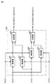
- FIG. It is a figure which shows the structure of the complex multiplication circuit which concerns on Embodiment 1.
- FIG. It is a time chart which shows the operation of the complex multiplication circuit shown in FIG.
- a time chart which shows the operation of the complex multiplication circuit shown in FIG.
- It is a time chart which shows the operation of the complex multiplication circuit shown in FIG.
- FIG. It is a time chart which shows the operation of the complex multiplication circuit shown in FIG.
- a time chart which shows the operation of the complex multiplication circuit shown in FIG.
- FIG. 1 is a diagram showing a configuration of a complex multiplication circuit according to the first embodiment.
- the complex multiplication circuit according to the first embodiment is configured to receive inputs of two complex numbers and output a value obtained by multiplying the two complex numbers.
- the complex multiplication circuit 100 receives the inputs of the first input signal X and the second input signal C.
- the first input signal X changes in the order of X 0 , X 1 , X 2 , ... In a predetermined cycle with a preset cycle.
- the second input signal C changes in the order of C 0 , C 1 , C 2 , ... In synchronization with the first input signal X.
- the first input signal X corresponds to one embodiment of the "first complex number”
- the second input signal C corresponds to one embodiment of the "second complex number”.
- the complex multiplication circuit 100 includes multiple circuits 1 to 5, a product difference calculation circuit 6, a product / sum calculation circuit 7, a flip-flop 8, and a clock generation circuit 9.
- the multiplex circuit 1 receives the real part Re (X) of the first input signal X and the imaginary part Im (X) of the first input signal X.
- the multiplex circuit 1 outputs a multiplex signal XI by time-dividing the input real number part Re (X) and the imaginary number part Im (X).
- the multiplex circuit 1 has a selector 10 and a flip-flop 12.
- the selector 10 receives inputs of the real number part Re (X) and the imaginary number part Im (X).
- the selector 10 time-division-multiplexes the real part Re (X) and the imaginary part Im (X) according to the logic (rising and falling) of the second clock signal CLK2, and outputs the multiplexed signal X.
- the multiplex circuit 1 corresponds to one embodiment of the "first multiplex circuit".
- the second clock signal CLK2 is generated by the clock generation circuit 9.
- the clock generation circuit 9 receives the first clock signal CLK1 having a frequency f [Hz].
- the frequency f [Hz] of the first clock signal CLK1 corresponds to twice the frequency of the input signals X and C.
- the clock generation circuit 9 generates the second clock signal CLK2 having a frequency f / 2 [Hz] by dividing the first clock signal CLK1 having a frequency f [Hz].
- the selector 10 outputs the imaginary part Im (X) at the rising timing of the second clock signal CLK2, and outputs the real part Re (X) at the falling timing of the second clock signal CLK2. That is, in the multiplex signal X output from the selector 10, the real part Re (X) and the imaginary part Im (X) appear alternately in the same period as the first clock signal CLK1.
- the flip-flop 12 receives the multiplex signal X output from the selector 10 and receives the first clock signal CLK1.
- the flip-flop 12 is a D flip-flop, which delays the input signal (multiplex signal X) by one cycle of the first clock signal CLK1 and outputs the multiplex signal XI.
- the multiplex circuit 2 receives the real part Re (C) of the second input signal C and the imaginary part Im (C) of the second input signal C.
- the multiplex circuit 2 outputs a multiplex signal CI by time-division multiplexing the input real number part Re (C) and imaginary number part Im (C).
- the multiplex circuit 2 corresponds to one embodiment of the "second multiplex circuit".
- the multiplex circuit 2 has a selector 20 and a flip-flop 22.
- the selector 20 receives the inputs of the real number part Re (C) and the imaginary number part Im (C).
- the selector 20 time-division-multiplexes the real number part Re (C) and the imaginary number part Im (C) according to the logic of the second clock signal CLK2, and outputs the multiplex signal C.
- the selector 20 outputs the imaginary part Im (C) at the rising timing of the second clock signal CLK2, and outputs the real number part Re (C) at the falling timing of the second clock signal CLK2.
- the flip-flop 22 is a D flip-flop, and the input signal (multiplex signal C) is delayed by one cycle of the first clock signal CLK1 to output the multiplex signal CI.
- the product difference calculation circuit 6 receives the multiplex signal XI from the multiplex circuit 1 and the multiplex signal CI from the multiplex circuit 2.
- the product difference calculation circuit 6 multiplies the multiplex signal XI and the multiplex signal CI in synchronization with the first clock signal CLK1.
- the product difference calculation circuit 6 further time-division-multiplexes the multiplication value B acquired in the current cycle and the value AB obtained by subtracting the multiplication value B from the multiplication value A acquired in the previous cycle, and multiplex signals. Output Q1.
- the product difference calculation circuit 6 corresponds to an embodiment of the “product difference calculation circuit”.
- the product difference calculation circuit 6 has a multiplier 60, a subtractor 62, a selector 64, and a flip-flop 66.
- the output signal B of the multiplier 60 is input to the subtractor 62 and the selector 64.
- the multiplier 60 corresponds to one embodiment of the "first multiplier".
- the subtractor 62 receives the output signal B of the multiplier 60 and the output signal A of the flip-flop 66.
- the subtractor 62 subtracts the output signal B from the output signal A and outputs the subtracted values AB.
- the output signals AB of the subtractor 62 are input to the selector 64.
- the subtractor 62 corresponds to one embodiment of the "subtractor".
- the selector 64 receives the inputs of the output signal B of the multiplier 60 and the output signals AB of the subtractor 62.
- the selector 64 time-division-multiplexes these two input signals according to the logic of the second clock signal CLK2, and outputs the multiplexed signal. Specifically, the selector 64 outputs the output signal B of the multiplier 60 at the rising timing of the second clock signal CLK2, and the output signal AB of the subtractor 62 at the falling timing of the second clock signal CLK2. Is output. That is, in the multiplex signal output from the selector 64, the multiplication value B and the subtraction value AB appear alternately in the same period as the first clock signal CLK1.
- the flip-flop 66 is a D flip-flop, and the input signal (output signal of the selector 64) is delayed by one cycle of the first clock signal CLK1 to output the multiplex signal Q1.
- the flip-flop 8 is a D flip-flop, which delays the multiplex signal CI input from the multiplex circuit 2 by one cycle of the first clock signal CLK1 and outputs the multiplex signal CII.
- the multiplex circuit 3 receives the multiplex signal XI from the multiplex circuit 1 and the multiplex signal CII from the flip-flop 8.
- the multiplex circuit 3 time-division-multiplexes the input multiplex signal XI and the multiplex signal CII and outputs the multiplex signal XI_CII.
- the multiplex circuit 3 has a selector 30 and a flip-flop 32.
- the selector 30 receives the inputs of the multiplex signal XI and the multiplex signal CII.
- the selector 30 time-division-multiplexes the multiplex signal XI and the multiplex signal CII according to the logic of the second clock signal CLK2, and outputs the multiplex signal. Specifically, the selector 30 outputs the multiplex signal XI at the rising timing of the second clock signal CLK2, and outputs the multiplex signal CII at the falling timing of the second clock signal CLK2. That is, in the multiplex signal output from the selector 30, the multiplex signal XI and the multiplex signal CII appear alternately in the same period as the first clock signal CLK1.
- the flip-flop 32 is a D flip-flop, and delays the input signal from the selector 30 by one cycle of the first clock signal CLK1 to output the multiplex signal XI_CII.
- the flip-flop 8 and the multiplex circuit 3 correspond to an embodiment of the "third multiplex circuit".
- the multiplex circuit 4 receives the multiplex signal C from the multiplex circuit 2 and the multiplex signal XI from the multiplex circuit 1.
- the multiplex circuit 4 time-division-multiplexes the input multiplex signal C and the multiplex signal XI and outputs the multiplex signal C_XI.
- the multiplex circuit 4 has a selector 40 and a flip-flop 42.
- the selector 40 receives the inputs of the multiplex signal XI and the multiplex signal C.
- the selector 40 time-division-multiplexes the multiplex signal C and the multiplex signal XI according to the logic of the second clock signal CLK2, and outputs the multiplex signal. Specifically, the selector 40 outputs the multiplex signal C at the rising timing of the second clock signal CLK2, and outputs the multiplex signal XI at the falling timing of the second clock signal CLK2. That is, in the multiplex signal output from the selector 40, the multiplex signal C and the multiplex signal XI appear alternately in the same period as the first clock signal CLK1.
- the flip-flop 42 is a D flip-flop, and delays the input signal from the selector 40 by one cycle of the first clock signal CLK1 to output the multiplex signal C_XI.
- the multiplex circuit 4 corresponds to one embodiment of the "fourth multiplex circuit".
- the product-sum calculation circuit 7 receives the multiplex signal XI_CII from the multiplex circuit 3 and the multiplex signal C_XI from the multiplex circuit 4.
- the product-sum calculation circuit 7 multiplies the multiplex signal XI_CII and the multiplex signal C_XI in synchronization with the first clock signal CLK1.
- the product-sum calculation circuit 7 further time-division-multiplexes the multiplication value C acquired in the current cycle and the value C + D obtained by adding the multiplication value D and the multiplication value C acquired in the previous cycle, and multiplex signals Q0. Is output.
- the product-sum calculation circuit 7 corresponds to an embodiment of the “product-sum calculation circuit”.
- the product-sum calculation circuit 7 has a multiplier 70, an adder 72, a selector 74, and a flip-flop 76.
- the output signal C of the multiplier 70 is input to the adder 72 and the selector 74.
- the multiplier 70 corresponds to one embodiment of the "second multiplier".
- the adder 72 receives the output signal C of the multiplier 70 and the output signal D of the flip-flop 76.
- the adder 72 adds the output signal C and the output signal D, and outputs the addition result C + D.
- the output signal C + D of the adder 72 is input to the selector 74.
- the adder 72 corresponds to one embodiment of the "adder".
- the selector 74 receives the input of the output signal C of the multiplier 70 and the output signal C + D of the adder 72.
- the selector 74 time-division-multiplexes these two input signals according to the logic of the second clock signal CLK2, and outputs the multiplexed signal. Specifically, the selector 74 outputs the output signal C + D of the adder 72 at the rising timing of the second clock signal CLK2, and outputs the output signal C of the multiplier 70 at the falling timing of the second clock signal CLK2. do. That is, in the multiplex signal output from the selector 74, the addition value C + D and the multiplication value C appear alternately in the same period as the first clock signal CLK1.
- the flip-flop 76 is a D flip-flop, and the input signal (output signal of the selector 74) is delayed by one cycle of the first clock signal CLK1 to output the multiplex signal Q0.
- the multiplex circuit 5 receives the multiplex signal Q1 from the product difference calculation circuit 6 and the multiplex signal Q0 from the product sum calculation circuit 7.
- the multiplex circuit 5 time-division-multiplexes the input multiplex signal Q1 and the multiplex signal Q0, and outputs the multiplex signal Q.
- the multiplex circuit 5 corresponds to one embodiment of the "fifth multiplex circuit".
- the multiplex circuit 5 has a selector 50 and a flip-flop 52.
- the selector 50 receives the input of the multiplex signal Q1 and the multiplex signal Q0
- the selector 50 time-division-multiplexes the multiplex signal Q1 and the multiplex signal Q0 according to the logic of the second clock signal CLK2, and outputs the multiplex signal.
- the selector 50 outputs the multiplex signal Q1 at the rising timing of the second clock signal CLK2, and outputs the multiplex signal Q0 at the falling timing of the second clock signal CLK2. That is, in the multiplex signal output from the selector 50, the multiplex signal Q1 and the multiplex signal Q0 appear alternately in the same period as the first clock signal CLK1.
- the flip-flop 52 is a D flip-flop, and delays the input signal from the selector 50 by one cycle of the first clock signal CLK1 to output the multiplex signal Q.
- the multiplex signal Q is an output signal of the complex multiplication circuit 100, and corresponds to a multiplication value of the first input signal X and the second input signal C, which are complex numbers.
- FIG. 2 and 3 are time charts showing the operation of the complex multiplication circuit 100 shown in FIG.
- the first clock signal CLK1, the second clock signal CLK2, the real part Re (X) and the imaginary part Im (X) of the first input signal X, and the real part Re of the second input signal C The waveforms of C) and the imaginary part Im (C) are shown.
- FIG. 2 also shows the multiplex signal X and the multiplex signal XI generated by the multiplex circuit 1, the multiplex signal C and the multiplex signal CI generated by the multiplex circuit 2, and the multiplex signal CII generated by the flip-flop 8.
- FIG. 2 further shows the waveforms of the multiplex signal Q1 generated by the product difference calculation circuit 6, the multiplex signal Q0 generated by the product sum calculation circuit 7, and the multiplex signal Q generated by the multiplex circuit 5.
- Is done. 3 shows the clock signals CLK1, CLK2, the real part Re (X) and the imaginary part Im (X) of the first input signal X, the real part Re (C) of the second input signal C, and the real part Re (C) of the second input signal C from the time chart of FIG.
- the waveforms of the imaginary part Im (C) and the multiplex signals Q1, Q0, and Q are extracted and shown.
- the first input signal X is a complex number X n (n is an integer of 0 or more) and has a real number part Re (X n ) and an imaginary number part Im (X n ).
- the second input signal C is a complex number C n and has a real part Re (C n ) and an imaginary part Im (C n ).
- the first input signal X changes in the order of X 0 , X 1 , X 2, ... At a predetermined cycle.
- the real part Re (X) changes in the order of Re (X 0 ), Re (X 1 ), Re (X 2 ), ...
- the imaginary part Im (X) is Im (X 0 ), Im ( It changes in the order of X 1 ), Im (X 2), ....
- the second input signal C changes in the order of C 0 , C 1 , C 2 , ...
- the real part Re (C) changes in the order of Re (C 0 ), Re (C 1 ), Re (C 2 ), ...
- the imaginary part Im (C) is Im (C 0 ), Im ( It changes in the order of C 1 ), Im (C 2), ....
- the first clock signal CLK1 has a frequency f [Hz] that is twice the frequency of the first input signal X and the second input signal C.
- the second clock signal CLK2 has a frequency f / 2 [Hz].
- the first clock signal CLK1 is given to flip-flops 8, 12, 22, 32, 42, 52, 66, and 76.
- the second clock signal CLK2 is given to selectors 10, 20, 30, 40, 50, 64, 74.
- the multiplex circuit 1 when the selector 10 receives the inputs of the real number part Re (X) and the imaginary number part Im (X) of the first input signal X, the real number part Re (X) is at the timing of the falling edge of the second clock signal CLK2. ) Is output, and the imaginary part Im (X) is output at the rising timing of the second clock signal CLK2. Therefore, the multiplex signal X output from the selector 10 is synchronized with the first clock signal CLK1 and is the real part Re (X 0 ), the imaginary part Im (X 0 ), the real part Re (X 1 ), and the imaginary part Im. It changes in the order of (X 1), ....
- the flip-flop 12 outputs a multiplex signal XI in which the multiplex signal X is delayed by one cycle of the first clock signal CLK1.
- the multiplex signal C output from the selector 20 is synchronized with the first clock signal CLK1 and is the real part Re (C 0 ), the imaginary part Im (C 0 ), the real part Re (C 1 ), and the imaginary part Im. It changes in the order of (C 1), ....
- the flip-flop 22 outputs a multiplex signal CI in which the multiplex signal C is delayed by one cycle of the first clock signal CLK1.
- the flip-flop 8 outputs a multiplex signal CII obtained by further delaying the multiplex signal CI given from the multiplex circuit 2 by one cycle of the first clock signal CLK1.
- the selector 30 when the selector 30 receives the input of the multiplex signal XI and the multiplex signal CII, it outputs the multiplex signal CII at the timing of the fall of the second clock signal CLK2, and at the timing of the rise of the second clock signal CLK2. Outputs the multiplex signal XI. Therefore, in the multiplex signal output from the selector 30, the multiplex signal XI and the multiplex signal CII appear alternately in synchronization with the first clock signal CLK1.
- the flip-flop 32 outputs a multiplex signal XI_CII in which the output signal of the selector 30 is delayed by one cycle of the first clock signal CLK1. As shown in FIG.
- the selector 40 when the selector 40 receives the input of the multiplex signal C and the multiplex signal XI, the selector 40 outputs the multiplex signal XI at the timing of the fall of the second clock signal CLK2, and at the timing of the rise of the second clock signal CLK2. Outputs the multiplex signal C. Therefore, in the multiplex signal output from the selector 40, the multiplex signal C and the multiplex signal XI appear alternately in synchronization with the first clock signal CLK1.
- the flip-flop 42 outputs a multiplex signal C_XI in which the output signal of the selector 40 is delayed by one cycle of the first clock signal CLK1. As shown in FIG.
- the product difference calculation circuit 6 receives the inputs of the multiplex signal XI and the multiplex signal CI.
- the multiplex signal XI is a multiplex signal in which the real part Re (X) and the imaginary part Im (X) of the first input signal X are time-division-multiplexed.
- the multiplex signal CI is a multiplex signal in which the real part Re (C) and the imaginary part Im (C) of the second input signal C are time-division-multiplexed.
- the multiplier 60 multiplies the multiplex signal XI and the multiplex signal CI in synchronization with the first clock signal CLK1.
- the multiplication value B of the multiplier 60 includes the multiplication value of the real part Re (X) and the real part Re (C), and the imaginary part Im (X) and the imaginary part Im (C) in synchronization with the first clock signal CLK1. ) Multiplies appear alternately.
- the subtractor 62 subtracts the multiplication value B acquired in the current cycle from the multiplication value A acquired in the previous cycle.
- the selector 64 outputs the multiplication value B of the multiplier 60 at the rising timing of the second clock signal CLK2, and outputs the subtraction value AB of the subtractor 62 at the falling timing of the second clock signal CLK2.
- the multiplication value B and the subtraction value AB appear alternately in the same cycle as the first clock signal CLK1.
- the flip-flop 66 outputs a multiplex signal Q1 in which the input signal (output signal of the selector 64) is delayed by one cycle of the first clock signal CLK1.
- the multiplex signal Q1 is synchronized with the first clock signal CLK1 and is the product of the real part Re (C 0 ) and the real part Re (X 0 ) [Re (C 0 ) Re. (X 0 )], the multiplication value [Re (C 0 ) Re (X 0 )] to the imaginary part Im (C 0 ) and the imaginary part Im (X 0 ) [Im (C 0 ) Im (I 0 ) ] Is subtracted from the value ⁇ Re (C 0 ) Re (X 0 ) -Im (C 0 ) Im (X 0 ) ⁇ , the multiplication value of the real part Re (X 1 ) and the real part Re (C 1) [Re ( C 1 ) Re (X 1 )], multiplication value [Re (C 1 ) Re (X 1 )] multiplied by imaginary part Im (C 1 ) and imaginary part Im (C 1 ) [Im (X 1 ) Im
- the multiple signal Q1 is the multiplication of the multiplication value [Re (C) Re (X)] of the real part Re (C) and the real part Re (X) and the real part Re (C) and the real part Re (X).
- a multi-signal in which the value ⁇ Re (C) Re (X) -Im (C) Im (X) ⁇ obtained by subtracting the multiplication value of the imaginary part Im (C) and the imaginary part Im (X) from the value is time-divided and multiplexed. Become.
- the product-sum calculation circuit 7 receives the inputs of the multiplex signal XI_CII and the multiplex signal C_XI.
- the multiplex signal XI_CII is a multiplex signal in which the real part Re (X) of the first input signal X and the real part Re (C) of the second input signal C are time-division-multiplexed.
- the multiplex signal C_XI is a multiplex signal in which the imaginary part Im (C) of the second input signal C and the imaginary part Im (X) of the first input signal X are time-division-multiplexed.
- the multiplier 70 multiplies the multiplex signal XI_CII and the multiplex signal C_XI in synchronization with the first clock signal CLK1.
- the multiplication value C of the multiplier 70 includes the multiplication value of the imaginary part Im (C) and the real part Re (X) and the real part Re (C) and the imaginary part Im (X) in synchronization with the first clock signal CLK1.
- Multiplies appear alternately.
- the adder 72 adds the multiplication value D acquired in the previous cycle and the multiplication value C acquired in the current cycle.
- the selector 74 outputs the multiplication value C of the multiplier 70 at the rising timing of the second clock signal CLK2, and outputs the addition value C + D at the rising timing of the second clock signal CLK2.
- the multiplication value C and the addition value C + D appear alternately in the same cycle as the first clock signal CLK1.
- the flip-flop 76 outputs a multiplex signal Q0 in which the input signal (output signal of the selector 74) is delayed by one cycle of the first clock signal CLK1.
- the multiplex signal Q0 is synchronized with the first clock signal CLK1 and is the product of the imaginary part Im (C 0 ) and the real part Re (X 0 ) [Im (C 0 ) Re.
- the multiple signal Q0 is the multiplication of the multiplication value [Im (C) Re (X)] of the imaginary part Im (C) and the real part Re (X) and the imaginary part Im (C) and the real part Re (X). It is a multiplex signal in which the value and the value ⁇ Im (C) Re (X) + Re (C) Im (X) ⁇ obtained by adding the multiplication value of the real part Re (C) and the imaginary part Im (X) are time-divided and multiplexed. ..
- the multiplex signal Q0 is delayed by one cycle of the first clock signal CLK1 with respect to the multiplex signal Q1. This is because the multiplex signals XI_CII and C_XI input to the product-sum calculation circuit 7 are delayed by one cycle of the first clock signal CLK1 with respect to the multiplex signals XI and CI input to the product difference calculation circuit 6. by.
- the selector 50 when the selector 50 receives the inputs of the multiplex signal Q1 and the multiplex signal Q0, it outputs the multiplex signal Q0 at the timing of the fall of the second clock signal CLK2, and at the timing of the rise of the second clock signal CLK2. Outputs the multiplex signal Q1. Therefore, in the multiplex signal output from the selector 50, the multiplex signal Q1 and the multiplex signal Q0 appear alternately in synchronization with the first clock signal CLK1.
- the flip-flop 52 outputs a multiplex signal Q in which the output signal of the selector 50 is delayed by one cycle of the first clock signal CLK1. As shown in FIGS.
- the multiplex signal Q changes in the order of subtraction value ⁇ Re (C) Re (X) -Im (C) Im (X) ⁇ and addition value ⁇ Im (C) Re (X) + Re (C) Im. (X) ⁇ is time-divided and multiplexed to obtain a multiplex signal.
- the multiplex signal Q is a multiplex signal in which the real part and the imaginary part of the multiplication value XC of the complex number X and the complex number C are time-division-multiplexed.
- the complex multiplication circuit converts each of the two complex numbers X and C into multiple signals XI and CI in which the real number part and the imaginary number part are time-divided and multiplexed, and is generated.
- the two multiplex signals XI and CI it is configured to output the multiplex signal Q in which the real part and the imaginary part are time-divided and multiplexed as the multiplication value XC.
- a circuit for arithmetically processing two multiplex signals X1 and CI may be configured to include two multipliers 60 and 70, one subtractor 62, and one adder 72. can.
- FIG. 4 shows the configuration of the conventional complex multiplication circuit 200 for comparison.
- the conventional complex multiplication circuit 200 receives the input of the complex number X and the complex number C shown in the equations (1) and (2) and outputs the multiplication value XC shown in the equation (3).
- it has four multipliers 201 to 204, one subtractor 205, and one adder 206.
- the multiplier 201 receives the inputs of the real part Re (X) of the complex number X and the real part Re (C) of the complex number C, and outputs the value Re (X) Re (C) obtained by multiplying these two inputs.
- the multiplier 202 receives the inputs of the imaginary part Im (X) of the complex number X and the imaginary part Im (C) of the complex number C, and outputs the value Im (X) Im (C) obtained by multiplying these two inputs.
- the multiplier 203 receives the imaginary part Im (X) of the complex number X and the real part Re (C) of the complex number C, and outputs the value Im (X) Re (C) obtained by multiplying these two inputs.
- the multiplier 204 receives the inputs of the real part Re (X) of the complex number X and the imaginary part Im (C) of the complex number C, and outputs the value Re (X) Im (C) obtained by multiplying these two inputs.
- the subtractor 205 subtracts the multiplication value Im (X) Im (C) of the multiplier 202 from the multiplication value Re (X) Re (C) of the multiplier 201, and the subtraction value ⁇ Re (X) Re (C)-. Im (X) Im (C) ⁇ is output.
- the adder 206 adds the multiplication value Im (X) Re (C) of the multiplier 203 and the multiplication value Re (X) Im (C) of the multiplier 204, and adds the addition value ⁇ Im (X) Re (C) + Re. (X) Im (C) ⁇ is output.
- the subtraction value of the subtractor 205 corresponds to the real part of the multiplication value XC of the complex number X and the complex number C
- the addition value of the adder 206 is the imaginary part of the multiplication value XC. It corresponds to.
- the conventional complex multiplier circuit 200 employs a circuit configuration having four multipliers, one subtractor, and one adder. In this circuit configuration, the multiplier has a larger amount of hardware than the adder and subtractor. Therefore, by mounting a large number of complex multiplication circuits for processing such as correlation detection, phase rotation, and detection, there is a concern that the circuit scale of the LSI will increase and the power consumption and cost will increase.
- the complex multiplication circuit 100 has a configuration in which a multiple signal obtained by time-dividing and multiplexing the real part and the imaginary part of each of the two complex numbers is calculated, so that the four multiplications required for the complex multiplication are performed by 2.
- Two multipliers can be shared and executed. As a result, the number of multipliers used can be reduced as compared with the conventional complex multiplier circuit 200, so that it is possible to prevent the LSI from becoming large and costly. Further, it is possible to suppress an increase in the power consumption of the LSI.
- the complex multiplication circuit 100 can be implemented in both an FPGA (Field Programmable Gate Array) and an ASIC (Application Specific Integrated Circuit). However, in the complex multiplication circuit 100, each of the product difference calculation circuit 6 and the product sum calculation circuit 7 is configured to be feasible by a DSP (Digital Signal Processor) dedicated circuit built in the FPGA.
- DSP Digital Signal Processor
- FIG. 5 is a diagram showing a configuration example of a general DSP dedicated circuit built in the FPGA.
- a general DSP dedicated circuit has a configuration in which an adder 302 (or a subtractor) is arranged after the multiplier 300.
- the producted calculated value is stored in the register, and the addition is repeated with respect to the calculated value.
- the product difference calculation circuit 6 and the product-sum calculation circuit 7 have an adder and a subtractor arranged after the multiplier, respectively, and the DSP dedicated circuit and the circuit shown in FIG.
- the configuration is common. Therefore, a general DSP dedicated circuit can be applied to each of the product difference calculation circuit 6 and the product sum calculation circuit 7.
- the complex multiplication circuit 100 can be easily mounted on the FPGA, and as a result, digital signal processing can be realized in a low-cost FPGA device.
- Embodiment 3 In the first embodiment, a configuration example of a complex multiplication circuit that receives inputs of a first complex number and a second complex number and outputs a value obtained by multiplying these two complex numbers has been described.
- FIG. 6 is a diagram showing a configuration of a complex multiplication circuit according to a third embodiment.
- the complex multiplication circuit 100A receives the inputs of the first input signal X and the second input signal C, similarly to the complex multiplication circuit 100 shown in FIG.
- the first input signal X changes in the order of X0, X1, X2, ... In a predetermined cycle with a preset cycle.
- the second input signal C changes in the order of C0, C1, C2, ... In synchronization with the first input signal X.
- the complex multiplication circuit 100A multiplies the first input signal X and the second input signal C and outputs the multiplication value XC as a signal Q (complex multiplication), and the complex conjugate X * and the first input signal X of the first input signal X. It is configured to selectively execute the operation of multiplying the two input signals C and outputting the multiplication value X * C as the signal Q (complex conjugate multiplication). However, the symbol * represents the complex conjugate.
- the complex multiplication circuit 100A receives a control signal S from a control circuit (not shown).
- the control circuit changes the control signal S between two values of "0 (L level)" and “1 (H level)". "0" corresponds to the "first level” and "1" corresponds to the "second level”.
- the control signal S is a control signal for switching between an operation of outputting the multiplication value XC and an operation of outputting the multiplication value X * C in the complex multiplication circuit 100A.
- the complex multiplication circuit 100A executes an operation of outputting the multiplication value XC when the control signal S is “0”, and outputs the multiplication value X * C when the control signal S is “1”. Perform the output operation.
- the complex multiplication circuit 100A executes an operation of outputting the multiplication value XC when the control signal S is “1”, and the multiplication value when the control signal S is “0”. It may be configured to execute the operation of outputting X * C.
- the complex multiplication circuit 100A includes multiple circuits 1 to 5, a product difference / product sum calculation circuit 6A, a product sum / product difference calculation circuit 7A, a flip-flop 8, and a clock generation circuit 9. To be equipped.
- the complex multiplication circuit 100A replaces the product-difference calculation circuit 6 and the product-sum calculation circuit 7 with the product-difference / product-sum calculation circuit 6A and the product-sum / product-difference calculation circuit. The difference is that it has 7A. Since the other configurations are the same as those of the complex multiplication circuit 100, the description will not be repeated.
- the product difference / product sum calculation circuit 6A receives the multiplex signal XI from the multiplex circuit 1, the multiplex signal CI from the multiplex circuit 2, and the control signal S from a control circuit (not shown).
- the product difference / product sum calculation circuit 6A multiplies the multiplex signal XI and the multiplex signal CI in synchronization with the first clock signal CLK1.
- the product difference / product sum calculation circuit 6A is a value obtained by subtracting the multiplication value B from the multiplication value B acquired in the current cycle and the multiplication value A acquired in the previous cycle.
- AB is time-divided and multiplexed, and the multiplex signal Q1 is output. That is, when the control signal S is "0", the product difference / product sum calculation circuit 6A operates as a product difference calculation circuit.
- the product difference / product sum calculation circuit 6A sets the multiplication value B acquired in the current cycle, and the multiplication value A and the multiplication value B acquired in the previous cycle.
- the added values A + B are time-division-multiplexed, and the multiplex signal Q1 is output. That is, when the control signal S is "1", the product difference / product sum calculation circuit 6A operates as a product sum calculation circuit.
- the product-difference / product-sum calculation circuit 6A has a multiplier 60, a subtraction / adder 68, a selector 64, and a flip-flop 66.
- the output signal B of the multiplier 60 is input to the subtractor / adder 68 and the selector 64.
- the subtraction / adder 68 receives the output signal B of the multiplier 60, the output signal A of the flip-flop 66, and the control signal S. When the control signal S is "0", the subtraction / adder 68 subtracts the output signal B from the output signal A and outputs the subtraction values AB. The output signals AB of the subtraction / adder 68 are input to the selector 64. On the other hand, when the control signal S is "1", the subtraction / adder 68 adds the output signal A and the output signal B and outputs the added value A + B. The output signals A + B of the subtraction / adder 68 are input to the selector 64.
- the subtraction / adder 68 corresponds to one embodiment of the "subtraction / adder".
- the selector 64 receives the input of the output signal B of the multiplier 60 and the output signal of the subtraction / adder 68 (subtraction value AB or addition value A + B).
- the selector 64 time-division-multiplexes these two input signals according to the logic of the second clock signal CLK2, and outputs the multiplexed signal. Specifically, the selector 64 outputs the output signal B of the multiplier 60 at the rising timing of the second clock signal CLK2, and outputs the output signal of the subtraction / adder 68 at the falling timing of the second clock signal CLK2. Output.
- the multiplication value B and the subtraction value AB appear alternately in the same cycle as the first clock signal CLK1.
- the flip-flop 66 is a D flip-flop, and the input signal (output signal of the selector 64) is delayed by one cycle of the first clock signal CLK1 to output the multiplex signal Q1.
- the product-sum / product-difference calculation circuit 7A receives the multiplex signal XI_CII from the multiplex circuit 3, the multiplex signal C_XI from the multiplex circuit 4, and the control signal S from a control circuit (not shown).
- the product-sum / product-difference calculation circuit 7A multiplies the multiplex signal XI_CII and the multiplex signal C_XI in synchronization with the first clock signal CLK1.
- the control signal S is "0”
- the product-sum / product-difference calculation circuit 7A adds the multiplication value C acquired in the current cycle, and the multiplication value D and the multiplication value C acquired in the previous cycle.
- the value C + D is time-division-multiplexed and the multiplex signal Q0 is output. That is, when the control signal S is "0", the product-sum / product-difference calculation circuit 7A operates as a product-sum calculation circuit.
- the product-sum / product difference calculation circuit 7A subtracts the multiplication value C from the multiplication value C acquired in the current cycle and the multiplication value D acquired in the previous cycle.
- the value DC is time-division-multiplexed and the multiplex signal Q0 is output. That is, when the control signal S is "1", the product-sum / product-difference calculation circuit 7A operates as the product-difference calculation circuit.
- the product-sum / product-difference calculation circuit 7A has a multiplier 70, an adder / subtractor 78, a selector 74, and a flip-flop 76.
- the output signal C of the multiplier 70 is input to the adder / subtractor 78 and the selector 74.
- the adder / subtractor 78 receives the output signal C of the multiplier 70, the output signal D of the flip-flop 76, and the control signal S. When the control signal S is "0", the adder / subtractor 78 adds the output signal C and the output signal D and outputs the added value C + D. The output signal C + D of the adder / subtractor 78 is input to the selector 74. On the other hand, when the control signal S is "1", the adder / subtractor 78 subtracts the output signal C from the output signal D and outputs the subtracted value DC. The output signal DC of the adder / subtractor 78 is input to the selector 74.
- the subtraction / adder 78 corresponds to one embodiment of the "adder / subtractor”.
- the selector 74 receives the input of the output signal C of the multiplier 70 and the output signal of the adder / subtractor 78 (adder value C + D or subtraction value DC).
- the selector 74 time-division-multiplexes these two input signals according to the logic of the second clock signal CLK2, and outputs the multiplexed signal. Specifically, the selector 74 outputs the output signal of the adder / subtractor 78 at the rising timing of the second clock signal CLK2, and outputs the output signal C of the multiplier 70 at the falling timing of the second clock signal CLK2. Output.
- the addition value C + D (or the subtraction value DC) and the multiplication value C appear alternately in the same cycle as the first clock signal CLK1.
- the flip-flop 76 is a D flip-flop, and the input signal (output signal of the selector 74) is delayed by one cycle of the first clock signal CLK1 to output the multiplex signal Q0.
- the multiplex circuit 5 receives the multiplex signal Q1 from the product / sum / sum calculation circuit 6A and the multiplex signal Q0 from the product / sum / sum / difference calculation circuit 7A.
- the multiplex circuit 5 time-division-multiplexes the input multiplex signal Q1 and the multiplex signal Q0, and outputs the multiplex signal Q.
- the complex multiplication circuit 100A executes an operation (complex multiplication) of outputting the multiplication value XC of the complex number X and the complex number C when the control signal S is “0”.
- the complex multiplication circuit 100A executes an operation (complex conjugate multiplication) of outputting the complex conjugate X * of the complex number X and the multiplication value X * C of the complex number C when the control signal S is “1”.
- FIG. 7 is a time chart showing the operation of the complex multiplication circuit 100A shown in FIG.
- the time chart shown in FIG. 7 shows the operation of the complex multiplication circuit 100A when the control signal S is “0”.
- the waveforms of the real part Re (C) and the imaginary part Im (C) are shown.
- 7 also shows the multiplex signal X and the multiplex signal XI generated by the multiplex circuit 1, the multiplex signal C and the multiplex signal CI generated by the multiplex circuit 2, and the multiplex signal CII generated by the flip-flop 8.
- the waveforms of the multiplex signal XI_CII generated by the multiplex circuit 3 and the multiplex signal C_XI generated by the multiplex circuit 4 are shown. Further, FIG.
- the first clock signal CLK1, the second clock signal CLK2, the real part Re (X) and the imaginary part Im (X) of the first input signal X, and the real part Re of the second input signal C The waveforms of (C) and the imaginary part Im (C), the multiplex signal X and the multiplex signal XI, the multiplex signal C and the multiplex signal CI, the multiplex signal CII, the multiplex signal XI_CII, and the multiplex signal C_XI are shown in the time chart shown in FIG. It is the same as the waveform of these signals.
- the multiplex signal Q1 and the multiplex signal Q0 are the same as the multiplex signal Q0 and the multiplex signal Q1 shown in FIGS. 2 and 3, respectively. Therefore, the multiplex signal Q is also the same as the multiplex signal Q shown in FIGS. 2 and 3. That is, the multiplex signal Q is a multiplex signal in which the real part and the imaginary part of the multiplication value XC of the complex number X and the complex number C are time-division-multiplexed.
- FIGS. 8 and 9 are time charts showing the operation of the complex multiplication circuit 100A shown in FIG.
- the time charts shown in FIGS. 8 and 9 show the operation of the complex multiplication circuit 100A when the control signal S is “1”.
- the first clock signal CLK1, the second clock signal CLK2, the control signal S the real part Re (X) and the imaginary part Im (X) of the first input signal X
- Waveforms of real and imaginary parts Re (C) and imaginary part Im (C) of the second input signal C multiplex signal X and multiplex signal XI, multiplex signal C and multiplex signal CI, multiplex signal CII, multiplex signal XI_CII, and multiplex signal C_XI.
- the first clock signal CLK1, the second clock signal CLK2, the real part Re (X) and the imaginary part Im (X) of the first input signal X, and the real part Re of the second input signal C The waveforms of (C) and the imaginary part Im (C), the multiplex signal X and the multiplex signal XI, the multiplex signal C and the multiplex signal CI, the multiplex signal CII, the multiplex signal XI_CII, and the multiplex signal C_XI are shown in the time chart shown in FIG. It is the same as the waveform of these signals.
- the multiplier 60 multiplies the multiplex signal XI and the multiplex signal CI in synchronization with the first clock signal CLK1 in the product difference / sum of products calculation circuit 6A.
- the multiplication value B of the multiplier 60 includes the multiplication value of the real part Re (X) and the real part Re (C), and the imaginary part Im (X) and the imaginary part Im (C) in synchronization with the first clock signal CLK1.
- Multiplies appear alternately.
- the subtraction / adder 68 adds the multiplication value A acquired in the previous cycle and the multiplication value B acquired in the current cycle.
- the selector 64 outputs the multiplication value B of the multiplier 60 at the rising timing of the second clock signal CLK2, and outputs the addition value A + B of the subtraction / adder 68 at the falling timing of the second clock signal CLK2.
- the multiplication value B and the addition value A + B appear alternately in the same cycle as the first clock signal CLK1.
- the flip-flop 66 outputs a multiplex signal Q1 in which the input signal (output signal of the selector 64) is delayed by one cycle of the first clock signal CLK1.
- the multiplex signal Q1 is synchronized with the first clock signal CLK1 and is a multiplication value of the real part Re (C0) and the real part Re (X0) [Re (C0) Re (X0). ]
- the multiple signal Q1 is the multiplication of the multiplication value [Re (C) Re (X)] of the real part Re (C) and the real part Re (X) and the real part Re (C) and the real part Re (X). It is a multiplex signal in which the value ⁇ Re (C) Re (X) + Im (C) Im (X) ⁇ , which is the sum of the value and the multiplication value of the imaginary part Im (C) and the imaginary part Im (X), is time-divided and multiplexed. ..
- the product-sum / product-difference calculation circuit 7A receives the inputs of the multiplex signal XI_CII and the multiplex signal C_XI.
- the multiplex signal XI_CII is a multiplex signal in which the real part Re (X) of the first input signal X and the real part Re (C) of the second input signal C are time-division-multiplexed.
- the multiplex signal C_XI is a multiplex signal in which the imaginary part Im (C) of the second input signal C and the imaginary part Im (X) of the first input signal X are time-division-multiplexed.
- the multiplier 70 multiplies the multiplex signal XI_CII and the multiplex signal C_XI in synchronization with the first clock signal CLK1.
- the multiplication value C of the multiplier 70 includes the multiplication value of the imaginary part Im (C) and the real part Re (X) and the real part Re (C) and the imaginary part Im (X) in synchronization with the first clock signal CLK1.
- Multiplies appear alternately.
- the adder / subtractor 78 subtracts the multiplication value C acquired in the current cycle from the multiplication value D acquired in the previous cycle.
- the selector 74 outputs the multiplication value C of the multiplier 70 at the rising timing of the second clock signal CLK2, and outputs the subtraction value DC at the rising timing of the second clock signal CLK2.
- the multiplication value C and the subtraction value DC appear alternately in the same cycle as the first clock signal CLK1.
- the flip-flop 76 outputs a multiplex signal Q0 in which the input signal (output signal of the selector 74) is delayed by one cycle of the first clock signal CLK1.
- the multiplex signal Q0 is synchronized with the first clock signal CLK1 and is the multiplication value of the imaginary part Im (C0) and the real part Re (X0) [Im (C0) Re (X0). ]
- the multiple signal Q0 is the multiplication of the multiplication value [Im (C) Re (X)] of the imaginary part Im (C) and the real part Re (X) and the imaginary part Im (C) and the real part Re (X).
- a multi-signal in which the value ⁇ Im (C) Re (X) -Re (C) Im (X) ⁇ obtained by subtracting the multiplication value of the real part Re (C) and the imaginary part Im (X) from the value is time-divided and multiplexed. Become.
- the multiplex signal Q0 is delayed by one cycle of the first clock signal CLK1 with respect to the multiplex signal Q1. This is because the multiple signals XI_CII and C_XI input to the product sum / product difference calculation circuit 7A are one cycle of the first clock signal CLK1 with respect to the multiple signals XI and CI input to the product difference / product sum calculation circuit 6A. Due to the delay of minutes.
- the selector 50 when the selector 50 receives the inputs of the multiplex signal Q1 and the multiplex signal Q0, it outputs the multiplex signal Q0 at the timing of the fall of the second clock signal CLK2, and at the timing of the rise of the second clock signal CLK2. Outputs the multiplex signal Q1. Therefore, in the multiplex signal output from the selector 50, the multiplex signal Q1 and the multiplex signal Q0 appear alternately in synchronization with the first clock signal CLK1.
- the flip-flop 52 outputs a multiplex signal Q in which the output signal of the selector 50 is delayed by one cycle of the first clock signal CLK1. As shown in FIGS.
- the multiplex signal Q is a multiplex signal in which the real part and the imaginary part of the multiplication value X * C of the complex conjugate X * and the complex number C are time-division-multiplexed.
- CI is converted to, and the generated two multiplex signals XI and CI are calculated to output a multiplex signal Q in which the real part and the imaginary part are time-divided and multiplexed as the multiplication value X * C. NS.
- the real number part and the imaginary number part are time-divided multiplex as the multiplication value XC as in the complex multiplication circuit according to the first embodiment. It is configured to output the multiple signal Q.
- the complex multiplication circuit according to the third embodiment has an operation of calculating the multiplication value XC of the complex number X and the complex number C according to the control signal S, and the multiplication value of the complex conjugate X * of the complex number X and the complex number C. It is possible to selectively execute the operation of calculating X * C.
- a circuit for arithmetically processing two multiplex signals XI and CI includes two multipliers 60 and 70, one subtractor / adder 68, and one adder / subtractor 78. Can be.
Landscapes
- Engineering & Computer Science (AREA)
- Physics & Mathematics (AREA)
- General Physics & Mathematics (AREA)
- Theoretical Computer Science (AREA)
- Computational Mathematics (AREA)
- Mathematical Analysis (AREA)
- Mathematical Optimization (AREA)
- Pure & Applied Mathematics (AREA)
- General Engineering & Computer Science (AREA)
- Computing Systems (AREA)
- Data Mining & Analysis (AREA)
- Mathematical Physics (AREA)
- Algebra (AREA)
- Databases & Information Systems (AREA)
- Software Systems (AREA)
- Complex Calculations (AREA)
- Time-Division Multiplex Systems (AREA)
Priority Applications (2)
| Application Number | Priority Date | Filing Date | Title |
|---|---|---|---|
| JP2021575626A JP7317151B2 (ja) | 2020-02-06 | 2020-12-02 | 複素乗算回路 |
| US17/790,833 US20230029006A1 (en) | 2020-02-06 | 2020-12-02 | Complex multiplication circuit |
Applications Claiming Priority (2)
| Application Number | Priority Date | Filing Date | Title |
|---|---|---|---|
| JP2020018788 | 2020-02-06 | ||
| JP2020-018788 | 2020-02-06 |
Publications (1)
| Publication Number | Publication Date |
|---|---|
| WO2021157172A1 true WO2021157172A1 (ja) | 2021-08-12 |
Family
ID=77200456
Family Applications (1)
| Application Number | Title | Priority Date | Filing Date |
|---|---|---|---|
| PCT/JP2020/044792 Ceased WO2021157172A1 (ja) | 2020-02-06 | 2020-12-02 | 複素乗算回路 |
Country Status (3)
| Country | Link |
|---|---|
| US (1) | US20230029006A1 (https=) |
| JP (1) | JP7317151B2 (https=) |
| WO (1) | WO2021157172A1 (https=) |
Families Citing this family (1)
| Publication number | Priority date | Publication date | Assignee | Title |
|---|---|---|---|---|
| US12045612B2 (en) * | 2022-09-12 | 2024-07-23 | International Business Machines Corporation | Special-purpose digital-compute hardware for efficient element-wise aggregation, scaling and offset |
Citations (3)
| Publication number | Priority date | Publication date | Assignee | Title |
|---|---|---|---|---|
| JPS5752959A (en) * | 1980-09-11 | 1982-03-29 | Mitsubishi Electric Corp | Multiplier |
| JPH1125071A (ja) * | 1997-06-28 | 1999-01-29 | Hyundai Electron Ind Co Ltd | 複素数乗算器 |
| JP2008506191A (ja) * | 2004-07-08 | 2008-02-28 | アソクス リミテッド | 可変サイズの高速直交変換を実施する方法および機器 |
Family Cites Families (4)
| Publication number | Priority date | Publication date | Assignee | Title |
|---|---|---|---|---|
| US8572153B1 (en) * | 2004-12-16 | 2013-10-29 | Xilinx, Inc. | Multiplier circuit configurable for real or complex operation |
| US7797366B2 (en) * | 2006-02-15 | 2010-09-14 | Qualcomm Incorporated | Power-efficient sign extension for booth multiplication methods and systems |
| US8386553B1 (en) * | 2006-12-05 | 2013-02-26 | Altera Corporation | Large multiplier for programmable logic device |
| US8543635B2 (en) * | 2009-01-27 | 2013-09-24 | Xilinx, Inc. | Digital signal processing block with preadder stage |
-
2020
- 2020-12-02 WO PCT/JP2020/044792 patent/WO2021157172A1/ja not_active Ceased
- 2020-12-02 US US17/790,833 patent/US20230029006A1/en active Pending
- 2020-12-02 JP JP2021575626A patent/JP7317151B2/ja active Active
Patent Citations (3)
| Publication number | Priority date | Publication date | Assignee | Title |
|---|---|---|---|---|
| JPS5752959A (en) * | 1980-09-11 | 1982-03-29 | Mitsubishi Electric Corp | Multiplier |
| JPH1125071A (ja) * | 1997-06-28 | 1999-01-29 | Hyundai Electron Ind Co Ltd | 複素数乗算器 |
| JP2008506191A (ja) * | 2004-07-08 | 2008-02-28 | アソクス リミテッド | 可変サイズの高速直交変換を実施する方法および機器 |
Also Published As
| Publication number | Publication date |
|---|---|
| US20230029006A1 (en) | 2023-01-26 |
| JP7317151B2 (ja) | 2023-07-28 |
| JPWO2021157172A1 (https=) | 2021-08-12 |
Similar Documents
| Publication | Publication Date | Title |
|---|---|---|
| Gustafsson | A difference based adder graph heuristic for multiple constant multiplication problems | |
| JP2004519917A (ja) | 改善されたノイズとスパー性能をもつσ−δn分周周波数分周器 | |
| WO2021157172A1 (ja) | 複素乗算回路 | |
| Butler et al. | Fast hardware computation of x mod z | |
| JPWO2021157172A5 (https=) | ||
| US20160291935A1 (en) | Spectral Shaping of Pseudorandom Binary Sequence | |
| US6441666B1 (en) | System and method for generating clock signals | |
| Safari et al. | Novel implementation of full adder based scaling in Residue Number Systems | |
| KR940001683A (ko) | 레이트 컨버터 | |
| Choudhary et al. | A SPT treatment to the realization of the sign-LMS based adaptive filters | |
| TW200426607A (en) | Method and apparatus of constructing a hardware architecture for transfer functions | |
| JP2005020554A (ja) | デジタルフィルタ | |
| JP2589809B2 (ja) | D/a変換器 | |
| KR100617141B1 (ko) | 디지털 필터 | |
| US6003055A (en) | Digital filter interpolation circuit | |
| TW202046647A (zh) | 數位類比轉換器裝置和數位類比轉換方法 | |
| JP3125225B2 (ja) | デジタル/アナログ変換器 | |
| KR100480068B1 (ko) | 디지탈 필터 | |
| CN100488049C (zh) | 数字滤波器 | |
| Thiel et al. | Digital asynchronous signal interpolation and clock domain crossing | |
| Ha et al. | A design of modular multiplier based on multi-precision carry save adder | |
| Srimol et al. | Distributed Arithmetic based Finite Impulse Response Filter Integrated with a Vedic Multiplier | |
| Choudhary et al. | A SPT treatment to the bit serial realization of the sign-LMS based adaptive filter | |
| Nagaratnam et al. | Power Optimized FPGA implementation of FIR Filter using Sub Component Minimization | |
| Dharaneesh et al. | Precision Clock: A Multi-Frequency Generator for Soc Application |
Legal Events
| Date | Code | Title | Description |
|---|---|---|---|
| 121 | Ep: the epo has been informed by wipo that ep was designated in this application |
Ref document number: 20917958 Country of ref document: EP Kind code of ref document: A1 |
|
| ENP | Entry into the national phase |
Ref document number: 2021575626 Country of ref document: JP Kind code of ref document: A |
|
| NENP | Non-entry into the national phase |
Ref country code: DE |
|
| 122 | Ep: pct application non-entry in european phase |
Ref document number: 20917958 Country of ref document: EP Kind code of ref document: A1 |