WO2021153461A1 - ヒータ基板、プローブカード用基板及びプローブカード - Google Patents
ヒータ基板、プローブカード用基板及びプローブカード Download PDFInfo
- Publication number
- WO2021153461A1 WO2021153461A1 PCT/JP2021/002299 JP2021002299W WO2021153461A1 WO 2021153461 A1 WO2021153461 A1 WO 2021153461A1 JP 2021002299 W JP2021002299 W JP 2021002299W WO 2021153461 A1 WO2021153461 A1 WO 2021153461A1
- Authority
- WO
- WIPO (PCT)
- Prior art keywords
- heater
- substrate
- conductor
- heater wire
- adjusting
- Prior art date
- Legal status (The legal status is an assumption and is not a legal conclusion. Google has not performed a legal analysis and makes no representation as to the accuracy of the status listed.)
- Ceased
Links
Images




Classifications
-
- G—PHYSICS
- G01—MEASURING; TESTING
- G01R—MEASURING ELECTRIC VARIABLES; MEASURING MAGNETIC VARIABLES
- G01R1/00—Details of instruments or arrangements of the types included in groups G01R5/00 - G01R13/00 and G01R31/00
- G01R1/02—General constructional details
- G01R1/06—Measuring leads; Measuring probes
- G01R1/067—Measuring probes
- G01R1/073—Multiple probes
- G01R1/07307—Multiple probes with individual probe elements, e.g. needles, cantilever beams or bump contacts, fixed in relation to each other, e.g. bed of nails fixture or probe card
- G01R1/07342—Multiple probes with individual probe elements, e.g. needles, cantilever beams or bump contacts, fixed in relation to each other, e.g. bed of nails fixture or probe card the body of the probe being at an angle other than perpendicular to test object, e.g. probe card
-
- H—ELECTRICITY
- H05—ELECTRIC TECHNIQUES NOT OTHERWISE PROVIDED FOR
- H05B—ELECTRIC HEATING; ELECTRIC LIGHT SOURCES NOT OTHERWISE PROVIDED FOR; CIRCUIT ARRANGEMENTS FOR ELECTRIC LIGHT SOURCES, IN GENERAL
- H05B3/00—Ohmic-resistance heating
- H05B3/20—Heating elements having extended surface area substantially in a two-dimensional [2D] plane, e.g. plate-heater
- H05B3/22—Heating elements having extended surface area substantially in a two-dimensional [2D] plane, e.g. plate-heater non-flexible
- H05B3/26—Heating elements having extended surface area substantially in a two-dimensional [2D] plane, e.g. plate-heater non-flexible heating conductor mounted on insulating base
- H05B3/265—Heating elements having extended surface area substantially in a two-dimensional [2D] plane, e.g. plate-heater non-flexible heating conductor mounted on insulating base the insulating base being an inorganic material, e.g. ceramic
-
- H—ELECTRICITY
- H05—ELECTRIC TECHNIQUES NOT OTHERWISE PROVIDED FOR
- H05B—ELECTRIC HEATING; ELECTRIC LIGHT SOURCES NOT OTHERWISE PROVIDED FOR; CIRCUIT ARRANGEMENTS FOR ELECTRIC LIGHT SOURCES, IN GENERAL
- H05B3/00—Ohmic-resistance heating
- H05B3/20—Heating elements having extended surface area substantially in a two-dimensional [2D] plane, e.g. plate-heater
- H05B3/22—Heating elements having extended surface area substantially in a two-dimensional [2D] plane, e.g. plate-heater non-flexible
- H05B3/28—Heating elements having extended surface area substantially in a two-dimensional [2D] plane, e.g. plate-heater non-flexible heating conductor embedded in insulating material
- H05B3/283—Heating elements having extended surface area substantially in a two-dimensional [2D] plane, e.g. plate-heater non-flexible heating conductor embedded in insulating material the insulating material being an inorganic material, e.g. ceramic
-
- G—PHYSICS
- G01—MEASURING; TESTING
- G01R—MEASURING ELECTRIC VARIABLES; MEASURING MAGNETIC VARIABLES
- G01R1/00—Details of instruments or arrangements of the types included in groups G01R5/00 - G01R13/00 and G01R31/00
- G01R1/02—General constructional details
- G01R1/06—Measuring leads; Measuring probes
- G01R1/067—Measuring probes
- G01R1/06711—Probe needles; Cantilever beams; "Bump" contacts; Replaceable probe pins
- G01R1/06755—Material aspects
- G01R1/06761—Material aspects related to layers
-
- G—PHYSICS
- G01—MEASURING; TESTING
- G01R—MEASURING ELECTRIC VARIABLES; MEASURING MAGNETIC VARIABLES
- G01R1/00—Details of instruments or arrangements of the types included in groups G01R5/00 - G01R13/00 and G01R31/00
- G01R1/02—General constructional details
- G01R1/06—Measuring leads; Measuring probes
- G01R1/067—Measuring probes
- G01R1/073—Multiple probes
-
- G—PHYSICS
- G01—MEASURING; TESTING
- G01R—MEASURING ELECTRIC VARIABLES; MEASURING MAGNETIC VARIABLES
- G01R1/00—Details of instruments or arrangements of the types included in groups G01R5/00 - G01R13/00 and G01R31/00
- G01R1/02—General constructional details
- G01R1/06—Measuring leads; Measuring probes
- G01R1/067—Measuring probes
- G01R1/073—Multiple probes
- G01R1/07307—Multiple probes with individual probe elements, e.g. needles, cantilever beams or bump contacts, fixed in relation to each other, e.g. bed of nails fixture or probe card
- G01R1/07314—Multiple probes with individual probe elements, e.g. needles, cantilever beams or bump contacts, fixed in relation to each other, e.g. bed of nails fixture or probe card the body of the probe being perpendicular to test object, e.g. bed of nails or probe with bump contacts on a rigid support
-
- G—PHYSICS
- G01—MEASURING; TESTING
- G01R—MEASURING ELECTRIC VARIABLES; MEASURING MAGNETIC VARIABLES
- G01R31/00—Arrangements for testing electric properties; Arrangements for locating electric faults; Arrangements for electrical testing characterised by what is being tested not provided for elsewhere
- G01R31/28—Testing of electronic circuits, e.g. by signal tracer
- G01R31/2851—Testing of integrated circuits [IC]
- G01R31/2855—Environmental, reliability or burn-in testing
- G01R31/286—External aspects, e.g. related to chambers, contacting devices or handlers
- G01R31/2863—Contacting devices, e.g. sockets, burn-in boards or mounting fixtures
-
- H—ELECTRICITY
- H05—ELECTRIC TECHNIQUES NOT OTHERWISE PROVIDED FOR
- H05B—ELECTRIC HEATING; ELECTRIC LIGHT SOURCES NOT OTHERWISE PROVIDED FOR; CIRCUIT ARRANGEMENTS FOR ELECTRIC LIGHT SOURCES, IN GENERAL
- H05B3/00—Ohmic-resistance heating
- H05B3/02—Details
-
- H—ELECTRICITY
- H05—ELECTRIC TECHNIQUES NOT OTHERWISE PROVIDED FOR
- H05B—ELECTRIC HEATING; ELECTRIC LIGHT SOURCES NOT OTHERWISE PROVIDED FOR; CIRCUIT ARRANGEMENTS FOR ELECTRIC LIGHT SOURCES, IN GENERAL
- H05B3/00—Ohmic-resistance heating
- H05B3/02—Details
- H05B3/03—Electrodes
-
- H—ELECTRICITY
- H05—ELECTRIC TECHNIQUES NOT OTHERWISE PROVIDED FOR
- H05B—ELECTRIC HEATING; ELECTRIC LIGHT SOURCES NOT OTHERWISE PROVIDED FOR; CIRCUIT ARRANGEMENTS FOR ELECTRIC LIGHT SOURCES, IN GENERAL
- H05B3/00—Ohmic-resistance heating
- H05B3/10—Heating elements characterised by the composition or nature of the materials or by the arrangement of the conductor
- H05B3/12—Heating elements characterised by the composition or nature of the materials or by the arrangement of the conductor characterised by the composition or nature of the conductive material
-
- H—ELECTRICITY
- H05—ELECTRIC TECHNIQUES NOT OTHERWISE PROVIDED FOR
- H05B—ELECTRIC HEATING; ELECTRIC LIGHT SOURCES NOT OTHERWISE PROVIDED FOR; CIRCUIT ARRANGEMENTS FOR ELECTRIC LIGHT SOURCES, IN GENERAL
- H05B3/00—Ohmic-resistance heating
- H05B3/10—Heating elements characterised by the composition or nature of the materials or by the arrangement of the conductor
- H05B3/16—Heating elements characterised by the composition or nature of the materials or by the arrangement of the conductor the conductor being mounted on an insulating base
-
- H—ELECTRICITY
- H05—ELECTRIC TECHNIQUES NOT OTHERWISE PROVIDED FOR
- H05B—ELECTRIC HEATING; ELECTRIC LIGHT SOURCES NOT OTHERWISE PROVIDED FOR; CIRCUIT ARRANGEMENTS FOR ELECTRIC LIGHT SOURCES, IN GENERAL
- H05B3/00—Ohmic-resistance heating
- H05B3/20—Heating elements having extended surface area substantially in a two-dimensional [2D] plane, e.g. plate-heater
- H05B3/22—Heating elements having extended surface area substantially in a two-dimensional [2D] plane, e.g. plate-heater non-flexible
- H05B3/28—Heating elements having extended surface area substantially in a two-dimensional [2D] plane, e.g. plate-heater non-flexible heating conductor embedded in insulating material
-
- H—ELECTRICITY
- H10—SEMICONDUCTOR DEVICES; ELECTRIC SOLID-STATE DEVICES NOT OTHERWISE PROVIDED FOR
- H10P—GENERIC PROCESSES OR APPARATUS FOR THE MANUFACTURE OR TREATMENT OF DEVICES COVERED BY CLASS H10
- H10P74/00—Testing or measuring during manufacture or treatment of wafers, substrates or devices
-
- G—PHYSICS
- G01—MEASURING; TESTING
- G01R—MEASURING ELECTRIC VARIABLES; MEASURING MAGNETIC VARIABLES
- G01R31/00—Arrangements for testing electric properties; Arrangements for locating electric faults; Arrangements for electrical testing characterised by what is being tested not provided for elsewhere
- G01R31/26—Testing of individual semiconductor devices
-
- G—PHYSICS
- G01—MEASURING; TESTING
- G01R—MEASURING ELECTRIC VARIABLES; MEASURING MAGNETIC VARIABLES
- G01R31/00—Arrangements for testing electric properties; Arrangements for locating electric faults; Arrangements for electrical testing characterised by what is being tested not provided for elsewhere
- G01R31/28—Testing of electronic circuits, e.g. by signal tracer
- G01R31/2851—Testing of integrated circuits [IC]
-
- H—ELECTRICITY
- H05—ELECTRIC TECHNIQUES NOT OTHERWISE PROVIDED FOR
- H05B—ELECTRIC HEATING; ELECTRIC LIGHT SOURCES NOT OTHERWISE PROVIDED FOR; CIRCUIT ARRANGEMENTS FOR ELECTRIC LIGHT SOURCES, IN GENERAL
- H05B2203/00—Aspects relating to Ohmic resistive heating covered by group H05B3/00
- H05B2203/014—Heaters using resistive wires or cables not provided for in H05B3/54
Definitions
- This disclosure relates to a heater substrate, a probe card substrate, and a probe card.
- Japanese Unexamined Patent Publication No. 2010-151497 discloses a probe card substrate used for electrical inspection of a wafer-shaped semiconductor element.
- This probe card substrate includes a heater substrate having a heater wire in the insulating substrate.
- the heater substrate according to the present disclosure is An insulating substrate having a first surface and a second surface opposite to the first surface, The heater wire located in the insulating substrate and An adjustment unit electrically connected to the heater wire and With The adjusting part A pair of adjustment terminals located on the second surface and electrically connected to both ends of a part of the heater wire, respectively. An adjustment conductor located on the second surface and connected to the pair of adjustment terminals, Have.
- the probe card substrate according to the present disclosure is The heater substrate having a plurality of first circuit conductors located from the first surface to the second surface and insulated from the heater wire.
- a circuit board located on the first surface of the heater board and having a plurality of second circuit conductors is provided.
- the plurality of second circuit conductors are connected to the plurality of first circuit conductors.
- the probe card according to this disclosure is The probe card substrate and a plurality of probe pins connected to the plurality of second circuit conductors are provided.
- FIG. 1A It is a top view of the 2nd surface side of the heater substrate which concerns on Embodiment 1 of this disclosure. It is sectional drawing in BB line of FIG. 1A. It is a top view of the 2nd surface side of the heater substrate which concerns on Embodiment 2 of this disclosure. It is a top view of the 2nd surface side of the heater substrate of the modification 1.
- FIG. It is a top view of the 2nd surface side of the heater substrate of the modification 3.
- FIG. 1A is a plan view of the second surface side of the heater substrate according to the first embodiment of the present disclosure.
- FIG. 1B shows a cross-sectional view taken along the line BB of FIG. 1A.
- the heater substrate 100 of the embodiment of the present disclosure includes an insulating substrate 1 having a first surface 11 and a second surface 12 opposite to the first surface, a heater wire 3 located in the insulating substrate 1, and a heater wire 3. It is provided with a plurality of adjusting units 5 electrically connected to a part of the sections SC1 to SC4.
- the insulating substrate 1 is a laminated body in which a plurality of ceramic insulating layers 1a are laminated, and has an insulating property.
- the heater wire 3 is a metallized conductor fired together with a plurality of ceramic insulating layers 1a, and is located between the plurality of ceramic insulating layers 1a and 1a.
- the material of the heater wire 3 is, for example, tungsten, but molybdenum or manganese may be applied, or an alloy metal containing a plurality of metal components such as tungsten, molybdenum, manganese, and copper may be adopted.
- the heater wire 3 has a line pattern that fills the heating region W1 of the insulating substrate 1, and generates Joule heat (heat generation) when a current is passed through the heater wire 3.
- the heating region W1 is a region set to be heated in the insulating substrate 1.
- the heating region W1 is a region in which the line pattern of the heater wire 3 is arranged, and corresponds to an arrangement region of the heater wire 3.
- the heating region W1 may be a region in which the object to be heated includes a portion facing the heater substrate 100.
- the heating region W1 is a region including a portion facing the wafer SW. There may be.
- Both ends of the heater wire 3 are connected to the feeding conductor 4.
- the power feeding conductor 4 includes a power feeding terminal 43 located on the second surface 12 and an internal conductor 42 located inside the insulating substrate 1 that electrically connects the power feeding terminal 43 and one end of the heater wire 3.
- the pair of power supply terminals 43 are terminals for supplying power to the heater wire 3.
- the inner conductor 42 is, for example, a via conductor extending in a direction perpendicular to the substrate surface (first surface 11 or second surface 12) of the insulating substrate 1, and is located from the second surface 12 to the heater wire 3.
- the inner conductor 42 may include a conductor extending in a direction along the substrate surface of the insulating substrate 1.
- the plurality of adjusting units 5 are connected in parallel with some sections SC1 to SC4 of the heater wire 3, respectively.
- Each adjusting unit 5 includes a pair of internal conductors 53 connected to both ends of the corresponding section SC1 (or SC2 to SC4) of the heater wire 3, a pair of adjusting terminals 51 connected to the pair of internal conductors 53, and a pair. It is provided with an adjusting conductor 52 connected between the adjusting terminals 51 of the above.
- the inner conductor 53 is, for example, a via conductor extending in a direction perpendicular to the substrate surface (first surface 11 or second surface 12) of the insulating substrate 1, and is located from the second surface 12 to the heater wire 3.
- the adjusting terminal 51 and the adjusting conductor 52 are located on the second surface 12.
- the inner conductor 53 is fired together with the plurality of ceramic insulating layers 1a.
- the feeding point of the heater wire 3 and the connecting point of the adjusting unit 5 may be the same point.
- the feeding terminal 43 and the adjusting terminal 51 are also used.
- the inner conductor 42 for power supply and the inner conductor 53 of the adjusting unit 5 are also used.
- the adjusting conductor 52 is made of a metal material (for example, copper) having a resistance ratio different from that of the heater wire 3.
- the specific resistance of the adjusting conductor 52 is smaller than the specific resistance of the heater wire 3, but it may be larger.
- the adjusting conductor 52 is formed by another pattern forming step after the firing step of the insulating substrate 1.
- the wire width, pattern length, thickness, and material of the adjusting conductor 52 are determined by the heater wire 3 and the adjusting unit 5 based on the measurement result of the resistance value of the heater wire 3 after firing the insulating substrate 1 including the heater wire 3.
- the current value flowing in the connected section SC1 (or SC2 to SC4) can be selected so as to approach the target value.
- the plurality of adjusting portions 5 are located on the outer peripheral portion in the heating region W1 and are dispersedly arranged on the second surface 12.
- the distributed arrangement means an arrangement in which the adjusting portion 5 is included in each divided region when the second surface 12 is divided into three or more equal angles from the center of the second surface 12 by radial dividing lines.
- the adjusting unit 5 is provided in each divided region. Means the included arrangement.
- the amount of heat generated varies from lot to lot or from individual to individual in the insulating substrate 1 after firing including the heater wire 3, or from the amount of heat generated or the target value for each region of the heating region W1.
- the error of such variation can be corrected. That is, after firing the insulating substrate 1 including the heater wire 3, the resistance of the heater wire 3 and each section SC1 to SC4 is measured, and the deviation from the target value of the resistance is calculated. Next, the resistance value of the adjusting conductor 52 is obtained so as to reduce these deviations, and the pattern and material of the adjusting conductor 52 are selected so as to realize the obtained resistance value.
- the adjusting conductor 52 on the second surface 12 of the insulating substrate 1, the above variation can be corrected, and the total calorific value of the heater wire 3 and the calorific value for each region can be brought close to the target values. Since the heater wire 3 is located inside the insulating substrate 1, it is difficult to trim the heater wire 3 after firing the insulating substrate 1, but by having the adjusting terminal 51 and the internal conductor 53 of the adjusting portion 5, After firing the insulating substrate 1, the adjusting conductor 52 can be connected to adjust the calorific value of the heater wire 3.
- the calorific value varies in each portion in the heating region W1, and the error from the desired target value of the calorific value varies.
- the specific resistance of the adjusting conductor 52 is different from the specific resistance of the heater wire 3, a conductor having a large specific resistance or a conductor having a small specific resistance can be adopted, and the resistance value of the adjusting conductor 52 can be changed. The degree of design freedom can be increased.
- FIG. 2 is a plan view of the heater substrate according to the second embodiment of the present disclosure on the second surface side.
- the heater substrate 100 of the second embodiment includes adjusting portions 5A and 5B located at the central portion C1 of the second surface 12.
- the central portion C1 of the insulating substrate 1 means the inside of an ellipse having a vertical dimension of 1/3 and a horizontal dimension of 1/3 centered on the vertical and horizontal centers of the second surface.
- the heat from the heater wire 3 is transferred to the first surface 11 side and the second surface 12 side, and is also along the substrate surface (first surface 11 or second surface 12). It is difficult to move in the direction because there is another section of the adjacent heater lines 3. Therefore, heat tends to be trapped in the central portion C1. Since the adjusting portions 5A and 5B located in the central portion C1 exert an action of reducing the amount of heat generated in the central portion C1, in the heater substrate 100 arranged so that the line pattern of the heater wire 3 fills the heating region, the central portion C1 Adjustment is easy when the heating temperature is made uniform inside and outside the.
- the heating temperature means the temperature of the first surface 11 when the heater wire 3 is driven.
- FIG. 3 to 5 are plan views of the heater substrates of Modifications 1 to 3 on the second surface side.
- the heater substrate 100 (FIG. 3) of the first modification has a symmetrical line pattern of the heater wire 3 and symmetrical adjusting portions 5C to 5F.
- the adjusting portions 5C and 5D are adjacent to each other, they are located at the central portion C1 of the second surface 12.
- One of the adjusting terminals 51 and the internal conductor 53 included in the adjusting unit 5C and one of the adjusting terminals 51 and the internal conductor 53 included in the adjacent adjusting unit 5D may be shared.
- one of the adjusting terminals 51 and the internal conductor 53 included in the adjusting unit 5E and one of the adjusting terminals 51 and the internal conductor 53 included in the adjacent adjusting unit 5F are shared. May be done.
- the amount of heat generated can be easily adjusted while maintaining the symmetrical distribution of heat generated. Further, when the target temperature distribution is bilaterally symmetric, but the characteristics of the heater wire 3 are deviated from the left-right symmetry, the adjusting conductors 52 of the adjusting portions 5C to 5F are set to different resistance values on the left and right, and the left and right are symmetrical. It is also possible to achieve a good calorific value distribution.
- the symmetrical adjustment portion may be located outside the central portion C1.
- the calorific value of the central portion C1 where heat tends to be trapped is reduced, and the heating temperature inside and outside the central portion C1 is reduced. It has the effect of facilitating the homogenization of.
- the heater substrate 100 may have an adjusting portion connected to the folded portion or the vicinity of the folded portion, and the adjusting portion may adjust the temperature of the folded portion to be lowered. Since the temperature of the folded-back portion in the central portion C1 tends to be higher, the heater substrate 100 has an adjusting portion connected to the folded-back portion of the central portion C1 or the vicinity of the folded-back portion, and the folded portion of the central portion C1 is provided by the adjusting portion. Adjustments may be made to lower the temperature of the section.
- the heater substrate 100 (FIG. 4) of the second modification includes an insulating substrate 1 having a rectangular substrate surface, a heater wire 3 having a meander pattern, and a plurality of adjusting portions 5G to 5J located in the central portion C1 of the substrate surface. Have. The adjusting portions 5G to 5J are connected to both ends of each section of the heater wire 3 overlapping the central portion C1.
- the heater wire 3 having a meander pattern enables a uniform amount of heat to be generated in each part of the rectangular region. Further, by having the adjusting portions 5G to 5J connected to both ends of each section of the heater wire 3 overlapping the central portion C1, it is possible to reduce heat buildup in the center of the heating region even in the rectangular heating region W1. , It is possible to make the heating temperature of the rectangular region uniform.
- one or a plurality of adjusting portions may be located outside the central portion C1, or the plurality of adjusting portions may be dispersedly arranged in the longitudinal direction of the insulating substrate 1.
- One adjustment unit may be connected so as to shortcut the meandering corner portion in the meander pattern. Also in the meander pattern, the temperature of the folded portion of the heater wire 3 as included in the region F2 tends to be high, but the folded portion of the meander pattern is located at the outer edge portion of the heating region W1 and easily dissipates heat. Therefore, the adjusting unit may be configured to be located at the central portion C1.
- the heater substrate 100 (FIG. 5) of the modified example 3 is located at an insulating substrate 1 having a rectangular substrate surface, heater wires 3a and 3b having a meander pattern and divided into two, and a central portion C1 of the substrate surface. It has adjusting units 5K and 5L.
- a pair of power supply terminals 43 electrically connected to both ends of one heater wire 3a and a pair of power supply terminals 43 electrically connected to both ends of the other heater wire 3b are located. do.
- the adjusting unit 5K is connected to a part of one heater line 3a, and the adjusting part 5L is connected to a part of the other heater line 3b.
- the plurality of heater wires 3a and 3a can be adjusted by adjusting the resistance of the adjusting units 5K and 5L.
- the calorific value of each of 3b can be adjusted.
- 6 to 12 are plan views showing the patterns of the heater wires of the modified examples 4 to 10. 6 to 12 show the space between the ceramic insulating layers 1a and 1a in which the heater wires 3A to 3M are arranged in the insulating substrate 1.
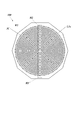
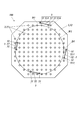
- the substrate surface of the insulating substrate 1 is an octagon that is symmetrical in the left-right and vertical directions, and the heater wire 3A has a spiral pattern in which both ends are located on the outer peripheral portion.
- the substrate surface of the insulating substrate 1 is square, and the heater wires 3B have a plurality of concentric sections having different diameters, and the plurality of sections are connected so as to be continuous. Has a pattern that has been made.
- the connecting portions of each section may be located in the angular range H1 above the paper surface of FIG. 7 from the center of the concentric circles, and the connecting portions of each section are distributed and arranged in a plurality of angular directions centered on the center of the concentric circles. May be good.
- the substrate surface of the insulating substrate 1 is a regular decagon
- the heater wire 3C has a plurality of concentric sections having different diameters, and the plurality of sections are continuous in one. Has a pattern connected to.
- the connecting portion of each section is located in the angle range H2 above the paper surface and the angle range H3 below the paper surface from the center of the concentric circles, and both ends of the heater wire 3C are located adjacent to each other on the outer peripheral portion of the heating region W1. You may.
- Modification 7 (FIG. 9) is an example in which the substrate surface of the insulating substrate 1 is a regular dodecagon, and has two heater wires 3D and 3E that are spiral and adjacent to each other from one end to the other end.
- the ends of the two heater wires 3D and 3E may be arranged at the center and the outer periphery of the heating region W1, respectively.
- the substrate surface of the insulating substrate 1 is circular, one heater wire 3F is located in the circular region W2 in the central portion of the heating region W1, and the heater wire 3F is located in the region W3 outside the region W2.
- the heater wire 3F has a plurality of concentric sections having different diameters, and has a pattern in which the plurality of sections are connected so as to be continuous.
- the heater wire 3G has a plurality of concentric sections having different diameters, and has a pattern in which the plurality of sections are connected so as to be continuous.
- the connecting portion of the plurality of sections of the heater wire 3F and the connecting portion of the plurality of sections of the heater wire 3G may be located at different ranges by 180 degrees at the central angle of the concentric sections.
- the substrate surface of the insulating substrate 1 is a regular octagon, and one heater wire 3H is located in one region W4 obtained by dividing the heating region W1 into two by the center line, and the other region W5.
- the heater wire 3H has a plurality of concentric semicircular sections having different diameters, and has a pattern in which the plurality of sections are connected so as to be continuous.
- the heater wire 3I may be the same as the pattern of the heater wire 3H, or may be a pattern symmetrical with respect to the boundary line between the regions W4 and W5.
- the substrate surface of the insulating substrate 1 and the heating region W1 are polygonal polygons symmetrical with respect to rotation of 90 degrees, and each region W6 obtained by dividing the heating region W1 into four at a central angle of 90 degrees.
- heater wires 3J to 3M are located one by one in each of W9.
- the heater wire 3J has a plurality of sections that are different in distance from the center of the heating region W1 and extend parallel to the sides of the heating region W1 and are bent at positions corresponding to the corners of the heating region W1. It has a pattern in which sections are connected so as to be continuous.
- the heater wire 3J has a straight section extending from the center of the heating region W1 to the outer peripheral portion, and one end of the heater wire 3I may be located on the outer peripheral portion by the straight section.
- the straight section is located across the boundaries of regions W6 and W7 that are adjacent to each other. By having such a straight section, both ends of the heater wire 3I can be arranged on the outer peripheral portion of the heating region W1.
- the pattern of the heater wires 3K to 3M may be the same as the pattern of the heater wires 3J.
- various shapes and patterns can be applied to the shape of the insulating substrate and the pattern of the heater wire as shown in the fourth to tenth embodiments.
- the temperature of the folded portion (connecting portion of each section) of the heater wire 3C as included in the angle ranges H2 and H3 in the modified example 6 (FIG. 8) also tends to increase.
- the temperature of the folded-back portion (connecting portion of each section) located at 1 and the folded-back portion (connecting portion of each section) of the heater wires 3J to 3M in the modified example 10 (FIG. 12) also tends to be high. Therefore, the heater substrate 100 may have an adjusting portion connected to the folded portion or the vicinity of the folded portion, and the adjusting portion may adjust the temperature of the folded portion to be lowered.
- the heater substrate 100 Since the temperature of the folded portion in the central portion tends to be higher, the heater substrate 100 has an adjusting portion connected to the folded portion in the central portion or the vicinity of the folded portion, and the temperature of the folded portion in the central portion is increased by the adjusting portion. Adjustments may be made to lower the temperature.
- the spiral heater wire has a folded portion where the temperature tends to increase. It is advantageous from the viewpoint of heat equalization because it does not contain or has few folded parts.
- the heater substrate may have an adjusting portion connected to the heater wire in this portion.
- the adjustment of the calorific value by this adjusting unit can reduce the influence on the heat soaking property on the object to be heated.
- FIG. 13A is a plan view of the second surface side of the heater substrate according to the third embodiment of the present disclosure.
- FIG. 13B shows a cross-sectional view taken along the line BB of FIG. 13A.
- the structure of the internal conductor 53A of the adjusting portion 5 and the arrangement of the adjusting terminal 51 and the adjusting conductor 52 are different from those of the first embodiment, and the other components are the same as those of the first embodiment. be.
- the different components will be described in detail.
- Each adjusting unit 5 has a pair of internal conductors 53A connected to both ends of a part of the heater wire 3 and a pair of adjusting terminals located on the second surface 12 and connected to the pair of internal conductors 53A, respectively. It includes a 51 and an adjusting conductor 52 connected to a pair of adjusting terminals 51.
- the inner conductor 53A includes a first inner conductor 53Aa and a third inner conductor 53Ac extending in a direction perpendicular to the substrate surface of the insulating substrate 1, and a second inner conductor extending in a direction along the substrate surface of the insulating substrate 1. It has 53Ab and.
- the first inner conductor 53Aa is connected to the heater wire 3 and the second inner conductor 53Ab and conducts the heater wire 3 and the second inner conductor 53Ab.
- the third inner conductor 53Ac is connected to the second inner conductor 53Ab and the adjusting terminal 51, and conducts the second inner conductor 53Ab and the adjusting terminal 51.
- the second inner conductor 53Ab is formed between the layers in which the heater wires 3 of the insulating substrate 1 are arranged (between the pair of adjacent ceramic insulating layers 1a and 1a) and the layers between the second surface 12 (adjacent pair). It is located between the ceramic insulating layers 1a and 1a).
- the second inner conductor 53Ab extends from the outer peripheral portion of the heater wire 3 to the outside of the heating region W1 when viewed from the direction perpendicular to the substrate surface of the insulating substrate 1.
- the heating region W1 corresponds to the arrangement region of the heater wire 3.
- the heating region W1 includes a region where the object to be heated faces, and may be larger than this region.
- the heating region W1 includes a region facing the wafer SW, which is the object to be heated, and may be larger than the region facing the wafer SW (FIG. 14A). reference).
- the third inner conductor 53Ac is connected to a portion of the second inner conductor 53Ab located outside the heating region W1, and the adjusting terminal 51 and the adjusting conductor 52 are located outside the heating region W1 (FIG. 13A). reference).
- the adjusting conductor 52 can be arranged on the peripheral edge of the second surface 12 as compared with the first embodiment. This is useful when there are many other components arranged in the center of the second surface 12 or in the heating region W1 and it is difficult to secure an arrangement space for the adjusting conductor 52.
- the heating region W1 may be larger than the region facing the heating target, and the outer peripheral portion of the heating region W1 may be out of the region facing the heating target. Since the outer peripheral portion of the heating region W1 has good heat dissipation, the temperature tends to be low, but even if the temperature is further lowered by the adjusting portion, if the objects to be heated do not face each other, the heat equalization to the object to be heated is affected. It has the advantage of being difficult.
- FIG. 14A is a plan view showing the probe card of the embodiment of the present disclosure.
- FIG. 14B is a cross-sectional view taken along the line BB of FIG. 14A.
- FIG. 15 is a plan view of the probe card substrate according to the embodiment of the present disclosure on the second surface side.
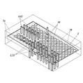
- FIG. 16 is a diagram showing an example of a structure in which a heater wire and a circuit conductor intersect.
- the probe card 700 of the embodiment of the present disclosure is a component incorporated in an apparatus for inspecting a plurality of semiconductor elements on a wafer SW, and a signal or a signal or a signal or a signal or a signal or a signal or a signal or It sends a voltage and receives a signal or voltage from a semiconductor element.
- the probe card 700 includes a probe card substrate 300 and a probe pin 400 fixed to the probe card substrate 300.
- the probe card substrate 300 includes a heater substrate 100 and a circuit board 200 located on the first surface 11 of the heater substrate 100.
- the heater substrate 100 includes a plurality of first circuit conductors 2 located from the first surface 11 to the second surface 12 and insulated from the heater wire 3. ..
- Each first circuit conductor 2 has a bonded conductor 21 located on the first surface 11, an internal conductor 22 located in the insulating substrate 1, and an external terminal 23 located on the second surface 12.
- One end of the inner conductor 22 is connected to the joint conductor 21, the other end is connected to the outer terminal 23, and the outer terminal 23 and the joint conductor 21 are electrically connected.
- the inner conductor 22 may include a portion extending in a direction perpendicular to the substrate surface of the heater substrate 100 and a portion extending in a direction along the substrate surface. As shown in FIG.
- the heater wire 3 has a through hole 30, and the internal conductor 22 arranged at a position intersecting the heater wire 3 passes through the through hole 30 of the heater wire 3 to form a through hole 30 with the heater wire 3. It is insulated and extends from the first surface 11 to the second surface 12 across the heater wires 3.
- the inner conductor 22 drawn as one in FIG. 14B may be a bundle of a plurality of inner conductors 22.
- the portion drawn as one in FIG. 1B may be a bundle of a plurality of inner conductors 42. The same applies to the internal conductor 53 of the adjusting unit 5 connected to the heater wire 3.
- a plurality of external terminals 23 of the first circuit conductor 2 are arranged on the second surface 12 of the heater substrate 100.
- the plurality of external terminals 23 are arranged apart from the adjusting terminal 51 and the adjusting conductor 52.
- the plurality of external terminals 23 are located so as to avoid the peripheral edge portion of the second surface 12.
- the adjustment terminal 51 and the adjustment conductor 52 are located on the peripheral edge of the second surface 12 of the adjustment terminal 51 and the adjustment conductor 52. It is advantageous because it is possible to prevent the 52 from narrowing the arrangement space of the external terminal 23.
- the circuit board 200 has a plurality of laminated resin insulating layers 210 and a second circuit conductor 220.
- the second circuit conductor 220 includes a plurality of junction conductors 221 located on the third surface 201 of the circuit board 200, a plurality of junction conductors 223 located on the fourth surface 202 opposite to the third surface 201, and the circuit board 200. It is located inside the third surface 201 to the fourth surface 202, and has a plurality of internal conductors 222 that electrically connect the plurality of joint conductors 221 and the plurality of joint conductors 223.
- the plurality of bonding conductors 221 are arranged corresponding to the terminals of the semiconductor element on the wafer SW, and the probe pins 400 are bonded to each.
- the plurality of joint conductors 223 are arranged corresponding to the plurality of joint conductors 21 of the heater substrate 100 and are connected to the plurality of joint conductors 21.
- the probe card 700 having the heater substrate 100, the heater substrate 100, the circuit board 200, and the wafer SW to be inspected can be heated by generating heat of the heater wire 3. Further, the adjusting unit 5 of the heater substrate 100 adjusts the calorific value of the heater wire 3 so as to reduce the variation of each lot or individual, or the variation of each portion in the heating region. Alternatively, the adjusting unit 5 adjusts the calorific value of the plurality of parts in the heating region W1 so as to approach a desired target value. Therefore, the wafer SW can be inspected under highly accurate temperature conditions.
- the ceramic insulating layer 1a of the insulating substrate 1 is made of, for example, a ceramic sintered body such as an aluminum oxide-based sintered body, an aluminum nitride-based sintered body, a silicon carbide sintered body, a mulite-based sintered body, or glass ceramics.
- a ceramic sintered body such as an aluminum oxide-based sintered body, an aluminum nitride-based sintered body, a silicon carbide sintered body, a mulite-based sintered body, or glass ceramics.
- Some of the mullite sintered bodies and glass ceramics have a smaller coefficient of thermal expansion than the other ceramic sintered bodies described above, and have a thermal expansion system close to the coefficient of thermal expansion of silicon on the substrate of the wafer SW to be inspected. is doing.
- the heater substrate 100 is used as the probe card 700 for inspection, the position of the electrode on the wafer SW and the probe pin 400 is unlikely to shift due to the temperature of the environment at the time of inspection. Therefore, it is possible to provide the probe card 700 having excellent inspection accuracy.
- these ceramic sintered bodies have high strength against mulite sintered bodies and glass ceramics. Since the thermal conductivity is also high, the rigidity is high and the heat generated in the heater wire 3 is excellent in thermal conductivity to the wafer SW.
- the insulating substrate 1 can be manufactured as follows, for example, when it is made of an aluminum oxide sintered body. First, a raw material powder containing aluminum oxide powder and a powder such as silicon oxide as a sintering aid component as a main component is kneaded with an organic solvent and a binder to form a slurry, and this slurry is used by a doctor blade method, a lip coater method, or the like. A ceramic green sheet (hereinafter, also referred to as a green sheet) to be a ceramic insulating layer 1a is produced by molding into a sheet by the molding method of the above. Next, a plurality of green sheets are laminated to prepare a laminated body. Then, the insulating substrate 1 can be produced by firing this laminated body at a temperature of about 1300 ° C. to 1600 ° C.
- a raw material powder containing aluminum oxide powder and a powder such as silicon oxide as a sintering aid component as a main component is kneaded with an organic
- the first circuit conductor 2 contains, for example, a metal material such as tungsten, molybdenum, manganese or copper, or an alloy material of these metal materials as a conductor component.
- these metal materials are sintered at the same time as the ceramic green sheet is fired to be formed as a metallized conductor on the surface and inside of the insulating substrate 1.
- it may contain an inorganic component such as glass or ceramics in order to increase the sinterability or the bonding strength with ceramics.
- the joint conductor 21 of the first circuit conductor 2 the inner conductor layer of the inner conductor 22 (the portion extending in the direction along the substrate surface), and the outer terminal 23 are, for example, a tungsten metallized layer, they are as follows. It can be formed in this way. For example, a metal paste prepared by mixing tungsten powder with an organic solvent and an organic binder is printed at a predetermined position on the green sheet to be the ceramic insulating layer 1a by a method such as a screen printing method and fired together with the green sheet. Can be formed.
- the via conductor (the portion extending in the direction perpendicular to the substrate surface) of the inner conductor 22 is provided with a through hole at a predetermined position on the green sheet prior to printing the above metal paste, and the same metal paste as above is provided. Can be formed by filling the through hole with.
- a nickel film of about 1 to 10 ⁇ m and a gold film of about 0.1 to 3 ⁇ m are sequentially formed to protect the surface and solder. It is possible to improve the bondability of materials and solder.
- the nickel film and the gold film can be formed of a plating film or a thin film obtained by electrolytic plating.
- the bonded conductor 21 can be formed of the metallized conductor as described above, but can also be formed of the wiring layer of the thin film conductor.
- the wiring layer of the thin film conductor can be produced, for example, as follows. For example, by using a thin film forming method such as a sputtering method, first, about 0.1 to 3 ⁇ m of titanium, chromium, or the like is bonded to the entire surface of the first surface 11 of the insulating substrate 1 having the inner conductor 22 and the outer terminal 23 of the metallized conductor. Form a metal layer. Next, a main conductor layer such as copper having a size of about 2 to 10 ⁇ m is formed on the entire surface of the bonded metal layer to form a conductive thin film layer. A barrier layer or the like may be formed if necessary. Then, the bonded conductor 21 of the thin film can be formed by pattern-processing the conductive thin film layer by photolithography.
- the first surface 11 of the insulating substrate 1 can be flattened by polishing or the like before forming the thin-film bonded conductor 21 on the first surface 11. As a result, the thin-film bonded conductor 21 can be formed with high accuracy.
- the heater wire 3 and the power supply terminal 43 of the power supply conductor 4 are the adjustment terminal 51 and the second inner conductor 53Ab of the adjustment unit 5, the joint conductor 21 of the first circuit conductor 2, the inner conductor layer and the outer terminal of the inner conductor 22. It can be formed with a metallized layer by the same material and method as in No. 23.
- As the metal paste for the heater wire 3 a metal paste obtained by adding a high resistance component such as ceramic particles to the metal paste for the first circuit conductor 2 can also be used.
- the through hole 30 of the heater wire 3 can be set by the screen pattern when screen printing on the green sheet.
- the inner conductor 42 of the power feeding conductor 4, the inner conductor 53 of the adjusting portion 5, the first inner conductor 53Aa, and the third inner conductor 53Ac can be formed by the same material and method as the via conductor of the inner conductor 22.
- the circuit board 200 includes a plurality of resin insulating layers 210 (resin insulating substrates) laminated as described above.
- the number and thickness of the resin insulating layer 210 are set according to the number of electrodes of the semiconductor element to be inspected, and are set so that they can be connected to the first circuit conductor 2 (junction conductor 21) of the heater substrate 100 and deployed.
- the resin insulating layer 210 includes, for example, a polyimide resin, a polyamideimide resin, a siloxane-modified polyamideimide resin, a siloxane-modified polyimide resin, a polyphenylene sulfide resin, a total aromatic polyester resin, a BCB (benzocyclobutene) resin, an epoxy resin, and bismaleimide triazine. It is made of an insulating resin such as a resin, a polyphenylene ether resin, a polyquinoline resin, and a fluororesin.
- the resin insulating layer 210 may contain a filler for adjusting the moldability and the coefficient of thermal expansion.
- the filler include barium sulfate, barium titanate, amorphous silica, crystalline silica, molten silica, spherical silica, talc, clay, magnesium carbonate, calcium carbonate, aluminum oxide, aluminum hydroxide, silicon nitride, and aluminum nitride.
- examples thereof include inorganic fillers such as boron nitride, alumina, magnesium oxide, magnesium hydroxide, titanium oxide, mica, talc, Neuburg silica soil, organic bentonite, and zirconium phosphate. One of these may be used alone, or two or more thereof may be used in combination as appropriate.
- the resin insulating substrate is formed, for example, by laminating and adhering a plurality of film-shaped resin insulating layers 210, applying a liquid precursor resin and curing the resin insulating layer 210 to form the resin insulating layer 210. It can be produced by repeating the step of forming the resin insulating layer 210 with the liquid precursor liquid resin. The method of laminating the film-shaped resin insulating layer 210 is more efficient.
- the joint conductors 221 and 223 of the second circuit conductor 220 and the inner conductor 222 may be formed as follows, for example. First, a resin insulating layer is formed with a resist film having openings corresponding to the via conductor (the portion extending in the direction perpendicular to the substrate surface) and the thin film wiring layer (the portion extending in the direction along the substrate surface) of the inner conductor 222. It is formed on the resin layer to be 210, and a recess corresponding to the thin film wiring layer and a through hole corresponding to the via conductor are formed by etching or laser processing.
- the joining reliability between the thin film wiring layer and the resin insulating layer 210 can be improved by providing the recess.
- a thin film forming method such as a thin film deposition method, a sputtering method, or an ion plating method, for example, a chromium (Cr) -copper (Cu) alloy layer or titanium (Ti)-is formed in the recesses and through holes of the resin insulating layer 210.
- a base conductor layer composed of a copper (Cu) alloy layer is formed.
- the internal conductor 222 can be formed by filling the recesses and through holes with a metal having a small electric resistance such as copper or gold by plating or the like and peeling off the resist.
- a nickel film of about 1 to 10 ⁇ m and a gold film of about 0.1 to 3 ⁇ m are sequentially formed on the surface of the bonded conductor 221 of the second circuit conductor 220 to protect the surface of the bonded conductor 221 and to protect the surface of the bonded conductor 221 and to protect the surface of the bonded conductor 221. It is possible to improve the bondability of solder and the like.
- the nickel film and the gold film can be formed of a plating film or a thin film obtained by electrolytic plating.
- the method of forming the heater substrate 100 and the circuit board 200 in a laminated structure is, for example, a method of producing the circuit board 200 and adhering it to the upper surface (first surface 11) of the heater substrate 100, or a method of adhering the circuit board 200 to the upper surface (first surface 11) of the heater substrate 100 (first surface 11).
- the method of laminating the resin insulating layers 210 layer by layer may be either a method using the film-like resin described above or a method using a liquid precursor resin. It is more efficient to prepare the circuit board 200 and bond the plurality of resin insulating layers 210 (and the second circuit conductor 220) to the upper surface (first surface 11) of the heater substrate 100 at once.
- the probe card 700 is formed by attaching the probe pin 400 to the second circuit conductor 220 (joint conductor 221) of the probe card substrate 300 manufactured in this manner.
- the probe pin 400 is mechanically and electrically connected to the bonding conductor 221.
- the probe pin 400 is made of a metal such as nickel or tungsten, for example. If the probe pin 400 is made of nickel, it is produced, for example, as follows. First, female molds of a plurality of probe pins are formed on one surface of a silicon substrate by etching. The female mold is arranged so as to correspond to the arrangement of the joint conductor 221 of the probe card substrate 300. Next, a metal made of nickel is adhered to the surface of the silicon substrate on which the female mold is formed by a plating method, and the female mold is further embedded with nickel. Other than the nickel embedded in the female mold, the nickel adhering to the upper surface of the silicon substrate is removed by processing such as an etching method to prepare a silicon substrate in which a nickel probe pin is embedded.
- the nickel probe pin embedded in the silicon substrate is bonded to the bonding conductor 221 of the probe card substrate 300 with a conductive bonding material such as solder. Then, by removing the silicon substrate with an aqueous potassium hydroxide solution, a probe card 700 in which the probe pin 400 is bonded to the bonding conductor 221 of the probe card substrate 300 can be obtained.
- the heater substrate, probe card substrate and probe card of the present disclosure are not limited to the above embodiments.
- the heater substrate may be applied to various other substrates that require heating.
- the number and arrangement of the adjusting portions, the section of the heater wire to which the adjusting portion is connected, and the pattern of the adjusting conductor shown in the above embodiment are merely examples and can be changed in various ways.
- the pattern of the adjusting conductor may be similar to or different from the pattern of the section of the heater wire to which the adjusting portion is connected.
- the details shown in the embodiment can be appropriately changed without departing from the spirit of the invention.
- This disclosure can be used for a heater substrate, a probe card substrate, and a probe card.
- Insulation substrate 1a Ceramic insulation layer 2 1st circuit conductor 3, 3A to 3M Heater wire 4 Feed conductor 11 1st surface 12 2nd surface 21 Join conductor 22 Internal conductor 23 External terminal 30 Through hole 42 Internal conductor 43 Power supply terminal 5, 5A to 5L Adjusting part 51 Adjusting terminal 52 Adjusting conductor 53, 53A Inner conductor 53Aa First inner conductor 53Ab Second inner conductor 53Ac Third inner conductor 100 Heater board 200 Circuit board 201 Third side 202 Fourth side 210 Resin insulation Layer 220 Second circuit conductor 221 223 Joint conductor 222 Inner conductor 300 Probe card substrate 400 Probe pin 700 Probe card C1 Central part SC1 to SC4 section SW Wafer W1 Heating area (placement area)
Landscapes
- Engineering & Computer Science (AREA)
- Physics & Mathematics (AREA)
- General Physics & Mathematics (AREA)
- Ceramic Engineering (AREA)
- Chemical & Material Sciences (AREA)
- Computer Hardware Design (AREA)
- General Engineering & Computer Science (AREA)
- Microelectronics & Electronic Packaging (AREA)
- Environmental & Geological Engineering (AREA)
- Inorganic Chemistry (AREA)
- Testing Or Measuring Of Semiconductors Or The Like (AREA)
- Resistance Heating (AREA)
- Testing Of Individual Semiconductor Devices (AREA)
- Measuring Leads Or Probes (AREA)
- Tests Of Electronic Circuits (AREA)
- Surface Heating Bodies (AREA)
Priority Applications (3)
| Application Number | Priority Date | Filing Date | Title |
|---|---|---|---|
| JP2021573998A JP7351938B2 (ja) | 2020-01-30 | 2021-01-22 | ヒータ基板、プローブカード用基板及びプローブカード |
| KR1020227025577A KR102829930B1 (ko) | 2020-01-30 | 2021-01-22 | 히터 기판, 프로브 카드용 기판 및 프로브 카드 |
| US17/795,981 US12174220B2 (en) | 2020-01-30 | 2021-01-22 | Heater substrate, probe card substrate, and probe card |
Applications Claiming Priority (2)
| Application Number | Priority Date | Filing Date | Title |
|---|---|---|---|
| JP2020013086 | 2020-01-30 | ||
| JP2020-013086 | 2020-01-30 |
Publications (1)
| Publication Number | Publication Date |
|---|---|
| WO2021153461A1 true WO2021153461A1 (ja) | 2021-08-05 |
Family
ID=77079077
Family Applications (1)
| Application Number | Title | Priority Date | Filing Date |
|---|---|---|---|
| PCT/JP2021/002299 Ceased WO2021153461A1 (ja) | 2020-01-30 | 2021-01-22 | ヒータ基板、プローブカード用基板及びプローブカード |
Country Status (4)
| Country | Link |
|---|---|
| US (1) | US12174220B2 (https=) |
| JP (1) | JP7351938B2 (https=) |
| KR (1) | KR102829930B1 (https=) |
| WO (1) | WO2021153461A1 (https=) |
Families Citing this family (1)
| Publication number | Priority date | Publication date | Assignee | Title |
|---|---|---|---|---|
| KR20230145459A (ko) * | 2022-03-30 | 2023-10-17 | 엔지케이 인슐레이터 엘티디 | 반도체 제조 장치용 부재 |
Citations (4)
| Publication number | Priority date | Publication date | Assignee | Title |
|---|---|---|---|---|
| US20020017916A1 (en) * | 1999-01-26 | 2002-02-14 | Simon Costello | Termperature-controlled semiconductor wafer chuck system |
| JP2002184558A (ja) * | 2000-12-12 | 2002-06-28 | Ibiden Co Ltd | ヒータ |
| JP2011069759A (ja) * | 2009-09-28 | 2011-04-07 | Kyocera Corp | プローブカード用基板,プローブカードおよびこれを用いた半導体ウエハ検査装置 |
| JP2017201669A (ja) * | 2016-05-06 | 2017-11-09 | 日本特殊陶業株式会社 | 加熱部材及び静電チャック |
Family Cites Families (14)
| Publication number | Priority date | Publication date | Assignee | Title |
|---|---|---|---|---|
| US5895591A (en) * | 1994-07-06 | 1999-04-20 | Ngk Spark Plug Co., Ltd. | Ceramic heater and oxygen sensor |
| JP2002246152A (ja) * | 2001-02-20 | 2002-08-30 | Ibiden Co Ltd | セラミックヒータ |
| JP2003077783A (ja) * | 2001-09-03 | 2003-03-14 | Ibiden Co Ltd | 半導体製造・検査装置用セラミックヒータおよびその製造方法 |
| TW200540430A (en) * | 2004-04-27 | 2005-12-16 | Jsr Corp | Sheet-like probe, method of producing the probe, and application of the probe |
| DE102008013978B4 (de) * | 2007-03-16 | 2021-08-12 | Cascade Microtech, Inc. | Chuck mit triaxialem Aufbau |
| KR100891384B1 (ko) * | 2007-06-14 | 2009-04-02 | 삼성모바일디스플레이주식회사 | 플렉서블 기판 접합 및 탈착장치 |
| JP5074878B2 (ja) * | 2007-10-15 | 2012-11-14 | 東京エレクトロン株式会社 | 検査装置 |
| JP5997899B2 (ja) * | 2008-07-18 | 2016-09-28 | ジェンサーム インコーポレイテッドGentherm Incorporated | 空調されるベッドアセンブリ |
| JP5199859B2 (ja) | 2008-12-24 | 2013-05-15 | 株式会社日本マイクロニクス | プローブカード |
| US9224626B2 (en) * | 2012-07-03 | 2015-12-29 | Watlow Electric Manufacturing Company | Composite substrate for layered heaters |
| JP6463938B2 (ja) | 2014-10-08 | 2019-02-06 | 日本特殊陶業株式会社 | 静電チャック |
| JP6703367B2 (ja) * | 2014-12-05 | 2020-06-03 | デクセリアルズ株式会社 | 加熱基板、保護素子および電子機器 |
| US20210005480A1 (en) * | 2019-07-01 | 2021-01-07 | Ramesh Divakar | Multi-zone silicon nitride wafer heater assembly having corrosion protective layer, and methods of making and using the same |
| WO2021107115A1 (ja) * | 2019-11-27 | 2021-06-03 | 京セラ株式会社 | 回路基板、プローブカード用基板およびプローブカード |
-
2021
- 2021-01-22 US US17/795,981 patent/US12174220B2/en active Active
- 2021-01-22 WO PCT/JP2021/002299 patent/WO2021153461A1/ja not_active Ceased
- 2021-01-22 JP JP2021573998A patent/JP7351938B2/ja active Active
- 2021-01-22 KR KR1020227025577A patent/KR102829930B1/ko active Active
Patent Citations (4)
| Publication number | Priority date | Publication date | Assignee | Title |
|---|---|---|---|---|
| US20020017916A1 (en) * | 1999-01-26 | 2002-02-14 | Simon Costello | Termperature-controlled semiconductor wafer chuck system |
| JP2002184558A (ja) * | 2000-12-12 | 2002-06-28 | Ibiden Co Ltd | ヒータ |
| JP2011069759A (ja) * | 2009-09-28 | 2011-04-07 | Kyocera Corp | プローブカード用基板,プローブカードおよびこれを用いた半導体ウエハ検査装置 |
| JP2017201669A (ja) * | 2016-05-06 | 2017-11-09 | 日本特殊陶業株式会社 | 加熱部材及び静電チャック |
Also Published As
| Publication number | Publication date |
|---|---|
| JP7351938B2 (ja) | 2023-09-27 |
| KR20220119693A (ko) | 2022-08-30 |
| US20230085111A1 (en) | 2023-03-16 |
| KR102829930B1 (ko) | 2025-07-04 |
| JPWO2021153461A1 (https=) | 2021-08-05 |
| US12174220B2 (en) | 2024-12-24 |
Similar Documents
| Publication | Publication Date | Title |
|---|---|---|
| CN110447079A (zh) | 检流电阻器 | |
| JP6999362B2 (ja) | ヒータ及びヒータシステム | |
| JP6140834B2 (ja) | 配線基板および電子装置 | |
| JP2007096246A (ja) | 配線基板およびそれを用いた電子装置 | |
| JP7308288B2 (ja) | 回路基板、プローブカード用基板およびプローブカード | |
| JP7351938B2 (ja) | ヒータ基板、プローブカード用基板及びプローブカード | |
| KR102804859B1 (ko) | 히터 기판, 프로브 카드용 기판 및 프로브 카드 | |
| JP5956185B2 (ja) | 多数個取り配線基板 | |
| US7110241B2 (en) | Substrate | |
| JP6683533B2 (ja) | 配線基板 | |
| JP2013207204A (ja) | 配線母基板 | |
| JP2011114019A (ja) | 回路モジュールおよび回路モジュールの実装方法 | |
| JP3911466B2 (ja) | 電子部品搭載基板および電子部品搭載構造体 | |
| US12306210B2 (en) | Multilayer circuit board with offset connection pads and inclined internal conductors for enhanced electrical connectivity | |
| JP7189061B2 (ja) | 回路基板、プローブカードおよび検査装置 | |
| JP2014086679A (ja) | 薄膜配線板、多層配線基板およびプローブカード用基板 | |
| JP2020181842A (ja) | 回路基板およびプローブカード | |
| JP2003273270A (ja) | 配線基板 | |
| JPWO2017082416A1 (ja) | 電子部品パッケージ | |
| JP6791771B2 (ja) | 検出素子搭載用基板、検出装置および検出モジュール | |
| JP2011077140A (ja) | 回路モジュールおよび回路モジュールの実装方法 | |
| KR20250114089A (ko) | 배선 기판 및 프로브 카드 | |
| JP2011077139A (ja) | 回路モジュールおよび回路モジュールの実装方法 | |
| JP2018006409A (ja) | 回路基板および電子装置 | |
| JP2012032166A (ja) | 配線基板およびプローブカード |
Legal Events
| Date | Code | Title | Description |
|---|---|---|---|
| 121 | Ep: the epo has been informed by wipo that ep was designated in this application |
Ref document number: 21748212 Country of ref document: EP Kind code of ref document: A1 |
|
| ENP | Entry into the national phase |
Ref document number: 2021573998 Country of ref document: JP Kind code of ref document: A |
|
| ENP | Entry into the national phase |
Ref document number: 20227025577 Country of ref document: KR Kind code of ref document: A |
|
| NENP | Non-entry into the national phase |
Ref country code: DE |
|
| 122 | Ep: pct application non-entry in european phase |
Ref document number: 21748212 Country of ref document: EP Kind code of ref document: A1 |