WO2021152825A1 - アンテナ装置、励振振幅制御装置及びレーダ装置 - Google Patents
アンテナ装置、励振振幅制御装置及びレーダ装置 Download PDFInfo
- Publication number
- WO2021152825A1 WO2021152825A1 PCT/JP2020/003698 JP2020003698W WO2021152825A1 WO 2021152825 A1 WO2021152825 A1 WO 2021152825A1 JP 2020003698 W JP2020003698 W JP 2020003698W WO 2021152825 A1 WO2021152825 A1 WO 2021152825A1
- Authority
- WO
- WIPO (PCT)
- Prior art keywords
- excitation amplitude
- antenna
- antenna elements
- excitation
- plane
- Prior art date
Links
Images


Classifications
-
- H—ELECTRICITY
- H01—ELECTRIC ELEMENTS
- H01Q—ANTENNAS, i.e. RADIO AERIALS
- H01Q21/00—Antenna arrays or systems
- H01Q21/06—Arrays of individually energised antenna units similarly polarised and spaced apart
- H01Q21/20—Arrays of individually energised antenna units similarly polarised and spaced apart the units being spaced along or adjacent to a curvilinear path
-
- H—ELECTRICITY
- H01—ELECTRIC ELEMENTS
- H01Q—ANTENNAS, i.e. RADIO AERIALS
- H01Q3/00—Arrangements for changing or varying the orientation or the shape of the directional pattern of the waves radiated from an antenna or antenna system
- H01Q3/26—Arrangements for changing or varying the orientation or the shape of the directional pattern of the waves radiated from an antenna or antenna system varying the relative phase or relative amplitude of energisation between two or more active radiating elements; varying the distribution of energy across a radiating aperture
- H01Q3/28—Arrangements for changing or varying the orientation or the shape of the directional pattern of the waves radiated from an antenna or antenna system varying the relative phase or relative amplitude of energisation between two or more active radiating elements; varying the distribution of energy across a radiating aperture varying the amplitude
Definitions
- the present disclosure relates to an antenna device including a plurality of antenna elements, an excitation amplitude control device that outputs an excitation amplitude to a feeding circuit, and a radar device including an antenna device.
- Patent Document 1 discloses an antenna device including a plurality of array antennas.
- the plurality of array antennas are arranged concentrically, and each array antenna includes a plurality of antenna elements arranged in a circumferential shape.
- the antenna device disclosed in Patent Document 1 suppresses unnecessary side lobes in the wide-angle direction by making the intervals of concentric circles unequal.
- the antenna device disclosed in Patent Document 1 has a problem that the first side lobe, which is a side lobe adjacent to the main lobe, cannot be suppressed even if the intervals of the concentric circles are unequal.
- the present disclosure has been made to solve the above-mentioned problems, and an object of the present disclosure is to obtain an antenna device provided with a plurality of antenna elements capable of suppressing the first side lobe.
- the antenna device acquires the excitation amplitudes of a plurality of antenna elements arranged on the plane and the plurality of antenna elements so as to surround one point on the plane, and according to the decibel value of each excitation amplitude.
- Each antenna element is provided with a feeding circuit for feeding power, and each excitation amplitude acquired by the feeding circuit is calculated based on each arrangement position in a plurality of antenna elements and multiplied by a correction coefficient larger than 1. Is what you are doing.
- the first side lobe can be suppressed.
- FIG. 5 is a hardware configuration diagram of a computer when the excitation amplitude control device 3 is realized by software, firmware, or the like. It is a flowchart which shows the processing procedure of the excitation amplitude control apparatus 3. Is an explanatory view showing a ⁇ ⁇
- antenna element 21-n (n 1, ⁇ , 8) excitation amplitude.
- FIG. 1 It is a block diagram which shows each of the antenna device 1 and the excitation amplitude control device 3 which concerns on Embodiment 2.
- FIG. 1 It is a block diagram which shows each of the antenna device 1 and the excitation amplitude control device 3 which concerns on Embodiment 2.
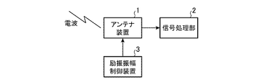
- FIG. 1 is a configuration diagram showing a radar device including the antenna device 1 according to the first embodiment.
- the radar device includes an antenna device 1, a signal processing unit 2, and an excitation amplitude control device 3.
- the antenna device 1 supplies power to each antenna element 21 according to the decibel value of the excitation amplitude of each antenna element 21 output from the excitation amplitude control device 3. After radiating the radio wave into the space, each antenna element 21 in the antenna device 1 receives the radio wave reflected by the target or the like and returned, and outputs the received signal of the radio wave to the signal processing unit 2.
- the signal processing unit 2 performs target detection processing, target tracking processing, and the like based on the received signal output from the antenna device 1. Since the target detection process is a known process, detailed description thereof will be omitted. Further, since the target tracking process is a known process, detailed description thereof will be omitted.
- the excitation amplitude control device 3 outputs the excitation amplitude of each of the N antenna elements 21 to the antenna device 1. Further, the excitation amplitude control device 3 outputs the correction coefficient of the excitation amplitude to the antenna device 1.
- FIG. 2 is a configuration diagram showing each of the antenna device 1 and the excitation amplitude control device 3 according to the first embodiment.
- the plane 11 is a plane parallel to the xy plane.
- N antenna elements 21 are arranged on the plane 11.
- One point 12 is the origin of the plane 11.
- one point 12 is assumed to be the origin of the plane 11.
- the one point 12 may be a point other than the origin of the plane 11.
- the first axis in the coordinate axes of the plane 11 is the x-axis
- the second axis in the coordinate axes of the plane 11 is the y-axis.
- the third axis, which is orthogonal to each of the first axis and the second axis, is the z-axis.
- the antenna element 21-n is realized by a monopole antenna.
- the antenna element 21-n may be realized by, for example, a dipole antenna.
- Each of the antenna elements 21-1 to 21-8 is arranged on a plane 11 so as to surround one point 12.
- the direction from the base end to the tip end of the antenna element 21-n is a direction parallel to the z-axis orthogonal to the xy plane.
- Dx is the opening diameter of the antenna device 1 in the direction parallel to the x-axis.
- Dy is the opening diameter of the antenna device 1 in the direction parallel to the y-axis.
- Feeding circuit 22, the excitation amplitude controller 3, the antenna element 21-n (n 1, ⁇ , 8) excitation amplitude of
- the power feeding circuit 22 when using the antenna element 21-n as a transmitting antenna, excitation amplitude
- I n ' log 10
- the power feeding circuit 22 multiplies the decibel value PRn of the power of the signal received by the antenna element 21-n by the correction coefficient ⁇ .
- the power supply circuit 22 outputs the decibel value PRn ⁇ ⁇ after multiplication by the correction coefficient to the signal processing unit 2.
- the excitation amplitude control device 3 includes an excitation amplitude calculation unit 31, an excitation amplitude storage unit 32, and an excitation amplitude output unit 33.
- FIG. 3 is a hardware configuration diagram showing the hardware of the excitation amplitude control device 3 according to the first embodiment.
- the excitation amplitude storage unit 32 is realized by, for example, the excitation amplitude storage circuit 42 shown in FIG. Excitation amplitude storage unit 32, the excitation amplitude after correction coefficient multiplication output from the excitation amplitude calculator 31
- ⁇ ⁇ ( n 1, ⁇ , 8) for storing.
- the excitation amplitude output unit 33 is realized by, for example, the excitation amplitude output circuit 43 shown in FIG. Excitation amplitude output section 33, the excitation amplitude after correction coefficient multiplication stored by excitation amplitude storage unit 32
- ⁇ ⁇ ( n 1, ⁇ , 8) , and the feeding circuit 22 of the antenna device 1 Output to. Further, the excitation amplitude output unit 33 outputs the correction coefficient ⁇ to the feeding circuit 22 of the antenna device 1.
- the excitation amplitude control device 3 shown in FIG. 2 includes an excitation amplitude calculation unit 31. However, this is only an example, and the excitation amplitude calculation unit 31 may be provided outside the excitation amplitude control device 3.
- each of the excitation amplitude calculation unit 31, the excitation amplitude storage unit 32, and the excitation amplitude output unit 33, which are the components of the excitation amplitude control device 3, is realized by dedicated hardware as shown in FIG. Is assumed. That is, it is assumed that the excitation amplitude control device 3 is realized by the excitation amplitude calculation circuit 41, the excitation amplitude storage circuit 42, and the excitation amplitude output circuit 43.
- the excitation amplitude storage circuit 42 includes, for example, a RAM (Random Access Memory), a ROM (Read Only Memory), a flash memory, an EPROM (Erasable Optical Read Online Memory), an EEPROM (Electrical Memory), or an EEPROM (Electrically). It corresponds to a sex semiconductor memory, a magnetic disk, a flexible disk, an optical disk, a compact disk, a mini disk, or a DVD (Digital Versaille Disc).
- each of the excitation amplitude calculation circuit 41 and the excitation amplitude output circuit 43 includes, for example, a single circuit, a composite circuit, a programmed processor, a parallel programmed processor, an ASIC (Application Specific Integrated Circuit), and an FPGA (Field-Programmable). Gate Array) or a combination of these is applicable.
- the components of the excitation amplitude control device 3 are not limited to those realized by dedicated hardware, and the excitation amplitude control device 3 is realized by software, firmware, or a combination of software and firmware. There may be.
- the software or firmware is stored as a program in the memory of the computer.
- a computer means hardware that executes a program, and corresponds to, for example, a CPU (Central Processing Unit), a central processing unit, a processing unit, an arithmetic unit, a microprocessor, a microcomputer, a processor, or a DSP (Digital Signal Processor). do.
- FIG. 4 is a hardware configuration diagram of a computer when the excitation amplitude control device 3 is realized by software, firmware, or the like.
- the excitation amplitude storage unit 32 is configured on the memory 51 of the computer.
- a program for causing the computer to execute the processing procedures of the excitation amplitude calculation unit 31 and the excitation amplitude output unit 33 is stored in the memory 51.
- the processor 52 of the computer executes the program stored in the memory 51.
- FIG. 3 shows an example in which each of the components of the excitation amplitude control device 3 is realized by dedicated hardware
- FIG. 4 shows an example in which the excitation amplitude control device 3 is realized by software, firmware, or the like. Shown. However, this is only an example, and some components in the excitation amplitude control device 3 may be realized by dedicated hardware, and the remaining components may be realized by software, firmware, or the like.
- FIG. 5 is a flowchart showing a processing procedure of the excitation amplitude control device 3.
- the antenna elements 21-1 ⁇ n by excitation amplitude calculating section 31 (n 1, ⁇ , N) excitation amplitude
- FIG. 2 illustrates d 7 which is the distance from the position where the antenna elements 21-7 are arranged to one point 12.
- the angle between the line segment connecting the position where the antenna element 21-n is arranged and the point 12 of the plane 11 and the x-axis is ⁇ n .
- FIG. 2 illustrates ⁇ 1 which is an angle between the x-axis and the line segment connecting the position where the antenna element 21-1 is arranged and the point 12.
- the beam direction is ⁇ 0 .
- FIG. 2 illustrates R 57 , which is the distance between the position where the antenna element 21-5 is arranged and the position where the antenna element 21-7 is arranged.
- the wave number of the radio wave forming the beam transmitted from the antenna elements 21-1 to 21-N or the beam received by the antenna elements 21-1 to 21-N is k.
- the characteristic impedance of the power supply circuit 22 is Z 0 .
- Excitation amplitude calculation unit 31 according to the following equation (1) and (2), as each of the excitation amplitude of the antenna elements 21-1 ⁇ 21-N, and calculates the absolute value of I 1 ⁇ I N.
- I n is the complex absolute value excitation amplitude of I n
- the argument of I n is the excitation phase.
- the antenna device 1 including the plurality of antenna elements 21 needs to obtain a high directivity gain
- a method of increasing the aperture diameter of the antenna is generally used. However, if the opening diameter of the antenna is increased, the installation area of the antenna device 1 becomes larger.
- Excitation amplitude calculation unit 31, according to equation (1) and (2), the antenna element 21-n (n 1, ⁇ , N) excitation amplitude
- a from 1 Is also multiplied by a large correction coefficient ⁇ (step ST2 in FIG. 5).
- excitation amplitude by excitation amplitude calculating section 31 calculates processing ⁇ alpha may be carried only once, every time the power supply circuit 22 is powered, excitation amplitude
- Excitation amplitude storage unit 32 the excitation amplitude after correction coefficient multiplication output from the excitation amplitude calculator 31
- ⁇ ⁇ ( n 1, ⁇ , 8) , and the feeding circuit 22 of the antenna device 1 (Step ST4 in FIG. 5). Further, the excitation amplitude output unit 33 outputs the correction coefficient ⁇ to the feeding circuit 22 of the antenna device 1.
- timing for outputting the respective ⁇ alpha and the correction coefficient alpha to the feeding circuit 22, power supply circuit 22 is equal to the before feeding to the antenna element 21-n, how The timing may be different.
- a ⁇ alpha and respective correction coefficient alpha to the feeding circuit 22 A mode of output is conceivable.
- Feeding circuit 22 when used antenna element 21-n as a transmitting antenna, excitation amplitude
- Feeding circuit 22 provides a decibel value I n ' ⁇ alpha to the antenna element 21-n.
- the power feeding circuit 22 multiplies the decibel value PRn of the power of the signal received by the antenna element 21-n by the correction coefficient ⁇ , and the decibel value after the correction coefficient multiplication. Outputs P Rn ⁇ ⁇ to the signal processing unit 2.
- the signal processing unit 2 performs target detection processing, target tracking processing, and the like based on the received signal output from the antenna device 1.
- the antenna element 21-n (n 1, ⁇ , 8) excitation amplitude of
- is an explanatory diagram showing a ⁇ ⁇
- the numbers on the horizontal axis indicate the element numbers of the antenna element 21, “1” is the antenna element 21-1, “2” is the antenna element 21-2, ..., “8” is the antenna.
- excitation amplitude in the case of alpha 1
- is ⁇ alpha excitation amplitude was calculated in accordance with equation (1) and (2)
- a corresponds to those not multiplied by a correction coefficient alpha.
- the antenna element 21-4 is an antenna element 21 arranged at one end of the antenna elements 21-1 to 21-8 in a direction parallel to the x-axis.
- the antenna element 21-8 is an antenna element 21 arranged at the other end of the antenna elements 21-1 to 21-8 in a direction parallel to the x-axis.
- ⁇ 1
- ⁇ ⁇ in the antenna elements 21-4 and 21-8 are the antenna elements 21-1 to 21.
- the numbers on the horizontal axis indicate the element numbers of the antenna element 21, “1” is the antenna element 21-1, “2” is the antenna element 21-2, ..., “8” is the antenna.
- is the excitation phase [psi n obtained when the is calculated
- the difference between the excitation phases ⁇ n of the two antenna elements 21 arranged adjacent to each other is 90 degrees or more.
- phase difference between the excitation phase [psi 2 of the excitation phase [psi 1 and the antenna element 21-2 of the antenna elements 21-1 is not less than 90 degrees
- the phase difference from the excitation phase ⁇ 3 of is 90 degrees or more.
- Phase difference between the excitation phase [psi 4 of the excitation phase [psi 3 and the antenna element 21-4 of the antenna elements 21-3 is not less than 90 degrees
- the phase difference from the phase ⁇ 5 is 90 degrees or more.
- Phase difference between the excitation phase [psi 6 of the excitation phase [psi 5 and the antenna element 21-6 of the antenna elements 21-5 is not less than 90 degrees, the excitation of the excitation phase [psi 6 and the antenna element 21-7 of the antenna elements 21-6
- the phase difference from the phase ⁇ 7 is 90 degrees or more.
- Phase difference between the excitation phase [psi 8 of the excitation phase [psi 7 and the antenna element 21-8 of the antenna elements 21-7 is not less than 90 degrees, the excitation of the excitation phase [psi 8 and the antenna element 21-1 of the antenna elements 21-8
- the phase difference from the phase ⁇ 1 is 90 degrees or more.
- the excitation phase distribution shown in FIG. 7 is common to the excitation phase distribution of the super gain antenna.
- the super gain antenna is known as an antenna capable of obtaining a high directional gain even if the aperture diameter of the antenna is small.
- the excitation phase distribution of the antenna device 1 is common to the excitation phase distribution of the super gain antenna. Therefore, the antenna device 1 can sharpen the beam in a specific direction and obtain a high directivity gain by taking the difference between the signals of the two antenna elements 21 arranged adjacent to each other.
- FIG. 8 is an explanatory diagram showing a simulation result of radiation characteristics in the antenna device 1 according to the first embodiment.
- the simulation conditions for radiation characteristics are as follows.
- ⁇ is a free space wavelength related to the frequency used by radio waves.
- a monopole antenna is used as the antenna element 21-n, and the length of the monopole antenna is 0.25 wavelength.
- Each of the antenna elements 21-1 to 21-8 is arranged at equal intervals. That is, each of the antenna elements 21-1 to 21-8 is arranged at an interval of 45 degrees around one point 12.
- ⁇ 0 [deg. ]
- ⁇ 90 [deg. ], A beam is formed.
- the radiation direction of the beam is 0 [deg. ]
- Main robe levels are about the same.
- the correction coefficient ⁇ may be 3, or the correction coefficient ⁇ may be 10.
- the excitation amplitude calculation unit 31 multiplies the excitation amplitudes
- the excitation amplitude calculation unit 31 multiplies each of the excitation amplitude
- by the correction coefficient ⁇ 1.9, and the excitation amplitude
- by the correction coefficient ⁇ 2.1.
- the excitation amplitudes of the plurality of antenna elements 21 arranged on the plane 11 and the plurality of antenna elements 21 so as to surround one point 12 of the plane 11 are acquired, and the respective excitation amplitudes are obtained.
- a feeding circuit 22 for feeding power to each antenna element 21 is provided according to the decibel value of, and each excitation amplitude acquired by the feeding circuit 22 is calculated based on the respective arrangement positions in the plurality of antenna elements 21.
- the antenna device 1 was configured so that a correction coefficient larger than 1 was multiplied. Therefore, the antenna device 1 can suppress the first side lobe.
- the antenna element 21-n (n 1) so that the opening diameter in the direction parallel to the x-axis is Dx and the opening diameter in the direction parallel to the y-axis is Dy. , ..., 8) are arranged on the outer circumference 13 of the ellipse.
- the distance between the positions where the two antenna elements 21 are arranged is 1. The distance may be less than or equal to the wavelength. In all combinations of the two antenna elements 21, if the distance between the positions where the two antenna elements 21 are arranged is one wavelength or less, the antenna device 1 having an aperture diameter of one wavelength or less in any direction is used. Obtainable.
- Embodiment 2 In the antenna device 1 shown in FIG. 2, the excitation amplitude control device 3 is provided outside the antenna device 1. However, this is only an example, and as shown in FIG. 9, the excitation amplitude control device 3 may be provided inside the antenna device 1.
- FIG. 9 is a configuration diagram showing each of the antenna device 1 and the excitation amplitude control device 3 according to the second embodiment. The operations of the antenna device 1 and the excitation amplitude control device 3 according to the second embodiment are the same as the operations of the antenna device 1 and the excitation amplitude control device 3 according to the first embodiment, respectively.
- the present disclosure is suitable for an antenna device including a plurality of antenna elements. Further, the present disclosure is suitable for an excitation amplitude calculation device that calculates the excitation amplitude of the antenna element. Further, the present disclosure is suitable for a radar device including an antenna device.
- Antenna device 1 Antenna device, 2 Signal processor, 3 Excitation amplitude control device, 11 Plane, 12 One point, 13 Outer circumference, 21-1 to 21-8 Antenna element, 22 Feed circuit, 31 Excitation amplitude calculation unit, 32 Excitation amplitude storage unit, 33 Excitation amplitude output unit, 41 Excitation amplitude calculation circuit, 42 Excitation amplitude storage circuit, 43 Excitation amplitude output circuit, 51 Memory, 52 Processor, 61, 62, 63 curves, 71, 72, 73 curves.
Abstract
平面(11)の一点(12)を囲むように、平面(11)に配置されている複数のアンテナ素子(21)と、複数のアンテナ素子(21)におけるそれぞれの励振振幅を取得し、それぞれの励振振幅のデシベル値に従って、それぞれのアンテナ素子(21)に給電する給電回路(22)とを備え、給電回路(22)により取得されるそれぞれの励振振幅が、複数のアンテナ素子(21)におけるそれぞれの配置位置に基づいて算出されて、1よりも大きな補正係数が乗算されているように、アンテナ装置(1)を構成した。
Description
本開示は、複数のアンテナ素子を備えるアンテナ装置と、励振振幅を給電回路に出力する励振振幅制御装置と、アンテナ装置を備えるレーダ装置とに関するものである。
以下の特許文献1には、複数のアレーアンテナを備えるアンテナ装置が開示されている。複数のアレーアンテナは、同心円状に配置されており、それぞれのアレーアンテナは、円周状に配置されている複数のアンテナ素子を備えている。
特許文献1に開示されているアンテナ装置は、同心円の間隔を不等間隔とすることによって、広角方向の不要なサイドローブを抑圧している。
特許文献1に開示されているアンテナ装置は、同心円の間隔を不等間隔とすることによって、広角方向の不要なサイドローブを抑圧している。
特許文献1に開示されているアンテナ装置では、同心円の間隔を不等間隔にしても、メインローブと隣接しているサイドローブである第1サイドローブを抑圧することができないという課題があった。
本開示は、上記のような課題を解決するためになされたもので、第1サイドローブを抑圧することができる、複数のアンテナ素子を備えるアンテナ装置を得ることを目的とする。
本開示に係るアンテナ装置は、平面の一点を囲むように、平面に配置されている複数のアンテナ素子と、複数のアンテナ素子におけるそれぞれの励振振幅を取得し、それぞれの励振振幅のデシベル値に従って、それぞれのアンテナ素子に給電する給電回路とを備え、給電回路により取得されるそれぞれの励振振幅が、複数のアンテナ素子におけるそれぞれの配置位置に基づいて算出されて、1よりも大きな補正係数が乗算されているものである。
本開示によれば、第1サイドローブを抑圧することができる。
以下、本開示をより詳細に説明するために、本開示を実施するための形態について、添付の図面に従って説明する。
実施の形態1.
図1は、実施の形態1に係るアンテナ装置1を備えるレーダ装置を示す構成図である。
レーダ装置は、アンテナ装置1、信号処理部2及び励振振幅制御装置3を備えている。
アンテナ装置1は、N個のアンテナ素子21(図2を参照)を備えている。Nは、2以上の整数である。
図2に示すアンテナ装置1では、N=8である例を示しており、N個のアンテナ素子21を区別するために、N個のアンテナ素子21を、アンテナ素子21-1~21-8のように表記している。
アンテナ装置1は、励振振幅制御装置3から出力されたそれぞれのアンテナ素子21の励振振幅のデシベル値に従って、それぞれのアンテナ素子21に給電する。
アンテナ装置1におけるそれぞれのアンテナ素子21は、電波を空間に放射した後、目標等に反射されて戻ってきた電波を受信し、電波の受信信号を信号処理部2に出力する。
信号処理部2は、アンテナ装置1から出力された受信信号に基づいて、目標の検出処理又は目標の追尾処理等を実施する。目標の検出処理は、公知の処理であるため詳細な説明を省略する。また、目標の追尾処理は、公知の処理であるため詳細な説明を省略する。
励振振幅制御装置3は、N個のアンテナ素子21におけるそれぞれの励振振幅をアンテナ装置1に出力する。
また、励振振幅制御装置3は、励振振幅の補正係数をアンテナ装置1に出力する。
励振振幅制御装置3は、N個のアンテナ素子21におけるそれぞれの励振振幅をアンテナ装置1に出力する。
また、励振振幅制御装置3は、励振振幅の補正係数をアンテナ装置1に出力する。
図2は、実施の形態1に係るアンテナ装置1及び励振振幅制御装置3のそれぞれを示す構成図である。
図2において、平面11は、x-y平面と平行な面である。平面11には、N個のアンテナ素子21が配置されている。
一点12は、平面11の原点である。
図2に示すアンテナ装置1では、説明の便宜上、一点12が、平面11の原点であるとしている。しかし、一点12は、平面11の原点以外の点であってもよい。
平面11の座標軸における第1の軸は、x軸であり、平面11の座標軸における第2の軸は、y軸である。
第1の軸及び第2の軸のそれぞれと直交している第3の軸は、z軸である。
図2において、平面11は、x-y平面と平行な面である。平面11には、N個のアンテナ素子21が配置されている。
一点12は、平面11の原点である。
図2に示すアンテナ装置1では、説明の便宜上、一点12が、平面11の原点であるとしている。しかし、一点12は、平面11の原点以外の点であってもよい。
平面11の座標軸における第1の軸は、x軸であり、平面11の座標軸における第2の軸は、y軸である。
第1の軸及び第2の軸のそれぞれと直交している第3の軸は、z軸である。
アンテナ素子21-n(n=1,・・・,8)は、例えば、モノポールアンテナによって実現される。
図2に示すアンテナ装置1では、アンテナ素子21-nがモノポールアンテナによって実現されている。しかし、これは一例に過ぎず、アンテナ素子21-nが、例えば、ダイポールアンテナによって実現されるものであってもよい。
アンテナ素子21-1~21-8のそれぞれは、一点12を囲むように、平面11に配置されている。
アンテナ素子21-n(n=1,・・・,8)は、一点12を中心とする楕円の外周13上に配置されている。
アンテナ素子21-nの基端から先端に至る方向は、x-y平面と直交しているz軸と平行な方向である。
図2に示すアンテナ装置1では、アンテナ素子21-nがモノポールアンテナによって実現されている。しかし、これは一例に過ぎず、アンテナ素子21-nが、例えば、ダイポールアンテナによって実現されるものであってもよい。
アンテナ素子21-1~21-8のそれぞれは、一点12を囲むように、平面11に配置されている。
アンテナ素子21-n(n=1,・・・,8)は、一点12を中心とする楕円の外周13上に配置されている。
アンテナ素子21-nの基端から先端に至る方向は、x-y平面と直交しているz軸と平行な方向である。
外周13は、一点12を中心とする楕円の外周であり、外周13には、アンテナ素子21-n(n=1,・・・,8)が配置されている。
Dxは、アンテナ装置1の開口径のうち、x軸と平行な方向での開口径である。
Dyは、アンテナ装置1の開口径のうち、y軸と平行な方向での開口径である。
Dxは、アンテナ装置1の開口径のうち、x軸と平行な方向での開口径である。
Dyは、アンテナ装置1の開口径のうち、y軸と平行な方向での開口径である。
給電回路22は、励振振幅制御装置3から、アンテナ素子21-n(n=1,・・・,8)の励振振幅|In|×αを取得する。|In|は、励振振幅制御装置3の後述する励振振幅算出部31により、補正係数αが乗算される前の励振振幅の絶対値であり、αは、1よりも大きな補正係数である。
また、給電回路22は、励振振幅制御装置3から、補正係数αを取得する。
給電回路22は、励振振幅|In|×αに従って、アンテナ素子21-nに給電する。
即ち、給電回路22は、アンテナ素子21-nを送信アンテナとして用いる場合、励振振幅|In|×αをデシベル値In ’×αに換算し、デシベル値In ’×αをアンテナ素子21-nに与える。In ’=log10|In|である。
給電回路22は、アンテナ素子21-nを受信アンテナとして用いる場合、アンテナ素子21-nにより受信された信号の電力のデシベル値PRnに、補正係数αを乗算する。
給電回路22は、補正係数乗算後のデシベル値PRn×αを信号処理部2に出力する。
励振振幅制御装置3は、励振振幅算出部31、励振振幅記憶部32及び励振振幅出力部33を備えている。
図3は、実施の形態1に係る励振振幅制御装置3のハードウェアを示すハードウェア構成図である。
図3は、実施の形態1に係る励振振幅制御装置3のハードウェアを示すハードウェア構成図である。
励振振幅算出部31は、例えば、図3に示す励振振幅算出回路41によって実現される。
励振振幅算出部31は、アンテナ素子21-1~21-8のそれぞれが配置されている位置に基づいて、アンテナ素子21-n(n=1,・・・,8)の励振振幅|In|を算出する。
励振振幅算出部31は、算出したアンテナ素子21-nの励振振幅|In|に、1よりも大きな補正係数αを乗算する。
励振振幅算出部31は、補正係数乗算後の励振振幅|In|×αを励振振幅記憶部32に出力する。
励振振幅算出部31は、アンテナ素子21-1~21-8のそれぞれが配置されている位置に基づいて、アンテナ素子21-n(n=1,・・・,8)の励振振幅|In|を算出する。
励振振幅算出部31は、算出したアンテナ素子21-nの励振振幅|In|に、1よりも大きな補正係数αを乗算する。
励振振幅算出部31は、補正係数乗算後の励振振幅|In|×αを励振振幅記憶部32に出力する。
励振振幅記憶部32は、例えば、図3に示す励振振幅記憶回路42によって実現される。
励振振幅記憶部32は、励振振幅算出部31から出力された補正係数乗算後の励振振幅|In|×α(n=1,・・・,8)を記憶する。
励振振幅出力部33は、例えば、図3に示す励振振幅出力回路43によって実現される。
励振振幅出力部33は、励振振幅記憶部32により記憶されている補正係数乗算後の励振振幅|In|×α(n=1,・・・,8)を、アンテナ装置1の給電回路22に出力する。
また、励振振幅出力部33は、補正係数αをアンテナ装置1の給電回路22に出力する。
励振振幅記憶部32は、励振振幅算出部31から出力された補正係数乗算後の励振振幅|In|×α(n=1,・・・,8)を記憶する。
励振振幅出力部33は、例えば、図3に示す励振振幅出力回路43によって実現される。
励振振幅出力部33は、励振振幅記憶部32により記憶されている補正係数乗算後の励振振幅|In|×α(n=1,・・・,8)を、アンテナ装置1の給電回路22に出力する。
また、励振振幅出力部33は、補正係数αをアンテナ装置1の給電回路22に出力する。
図2に示す励振振幅制御装置3は、励振振幅算出部31を備えている。しかし、これは一例に過ぎず、励振振幅算出部31が、励振振幅制御装置3の外部に設けられていてもよい。
図2では、励振振幅制御装置3の構成要素である励振振幅算出部31、励振振幅記憶部32及び励振振幅出力部33のそれぞれが、図3に示すような専用のハードウェアによって実現されるものを想定している。即ち、励振振幅制御装置3が、励振振幅算出回路41、励振振幅記憶回路42及び励振振幅出力回路43によって実現されるものを想定している。
励振振幅記憶回路42は、例えば、RAM(Random Access Memory)、ROM(Read Only Memory)、フラッシュメモリ、EPROM(Erasable Programmable Read Only Memory)、EEPROM(Electrically Erasable Programmable Read Only Memory)等の不揮発性又は揮発性の半導体メモリ、磁気ディスク、フレキシブルディスク、光ディスク、コンパクトディスク、ミニディスク、あるいは、DVD(Digital Versatile Disc)が該当する。
また、励振振幅算出回路41及び励振振幅出力回路43のそれぞれは、例えば、単一回路、複合回路、プログラム化したプロセッサ、並列プログラム化したプロセッサ、ASIC(Application Specific Integrated Circuit)、FPGA(Field-Programmable Gate Array)、又は、これらを組み合わせたものが該当する。
また、励振振幅算出回路41及び励振振幅出力回路43のそれぞれは、例えば、単一回路、複合回路、プログラム化したプロセッサ、並列プログラム化したプロセッサ、ASIC(Application Specific Integrated Circuit)、FPGA(Field-Programmable Gate Array)、又は、これらを組み合わせたものが該当する。
励振振幅制御装置3の構成要素は、専用のハードウェアによって実現されるものに限るものではなく、励振振幅制御装置3が、ソフトウェア、ファームウェア、又は、ソフトウェアとファームウェアとの組み合わせによって実現されるものであってもよい。
ソフトウェア又はファームウェアは、プログラムとして、コンピュータのメモリに格納される。コンピュータは、プログラムを実行するハードウェアを意味し、例えば、CPU(Central Processing Unit)、中央処理装置、処理装置、演算装置、マイクロプロセッサ、マイクロコンピュータ、プロセッサ、あるいは、DSP(Digital Signal Processor)が該当する。
ソフトウェア又はファームウェアは、プログラムとして、コンピュータのメモリに格納される。コンピュータは、プログラムを実行するハードウェアを意味し、例えば、CPU(Central Processing Unit)、中央処理装置、処理装置、演算装置、マイクロプロセッサ、マイクロコンピュータ、プロセッサ、あるいは、DSP(Digital Signal Processor)が該当する。
図4は、励振振幅制御装置3が、ソフトウェア又はファームウェア等によって実現される場合のコンピュータのハードウェア構成図である。
励振振幅制御装置3が、ソフトウェア又はファームウェア等によって実現される場合、励振振幅記憶部32がコンピュータのメモリ51上に構成される。励振振幅算出部31及び励振振幅出力部33の処理手順をコンピュータに実行させるためのプログラムがメモリ51に格納される。そして、コンピュータのプロセッサ52が、メモリ51に格納されているプログラムを実行する。
励振振幅制御装置3が、ソフトウェア又はファームウェア等によって実現される場合、励振振幅記憶部32がコンピュータのメモリ51上に構成される。励振振幅算出部31及び励振振幅出力部33の処理手順をコンピュータに実行させるためのプログラムがメモリ51に格納される。そして、コンピュータのプロセッサ52が、メモリ51に格納されているプログラムを実行する。
また、図3では、励振振幅制御装置3の構成要素のそれぞれが専用のハードウェアによって実現される例を示し、図4では、励振振幅制御装置3が、ソフトウェア又はファームウェア等によって実現される例を示している。しかし、これは一例に過ぎず、励振振幅制御装置3における一部の構成要素が専用のハードウェアによって実現され、残りの構成要素がソフトウェア又はファームウェア等によって実現されるものであってもよい。
次に、図2に示すアンテナ装置1及び励振振幅制御装置3におけるそれぞれの動作について説明する。
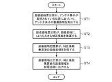
図5は、励振振幅制御装置3の処理手順を示すフローチャートである。
図5は、励振振幅制御装置3の処理手順を示すフローチャートである。
励振振幅制御装置3の励振振幅算出部31は、アンテナ素子21-1~21-8のそれぞれが配置されている位置に基づいて、アンテナ素子21-n(n=1,・・・,8)の励振振幅|In|を算出する(図5のステップST1)。
以下、励振振幅算出部31によるアンテナ素子21-1~n(n=1,・・・,N)の励振振幅|In|の算出処理を具体的に説明する。
以下、励振振幅算出部31によるアンテナ素子21-1~n(n=1,・・・,N)の励振振幅|In|の算出処理を具体的に説明する。
ここでは、アンテナ素子21-nが配置されている位置から、平面11の一点12までの距離がdnであるとする。図2では、アンテナ素子21-7が配置されている位置から一点12までの距離であるd7を例示している。
アンテナ素子21-nが配置されている位置と平面11の一点12とを結ぶ線分と、x軸との角度がφnである。図2では、アンテナ素子21-1が配置されている位置と一点12とを結ぶ線分と、x軸との角度であるφ1を例示している。
アンテナ素子21-1~21-Nから送信されるビーム、又は、アンテナ素子21-1~21-Nにより受信されるビームの方向のうち、平面11と平行な面内でのビーム方向がφ0である。
アンテナ素子21-1~21-Nから送信されるビーム、又は、アンテナ素子21-1~21-Nにより受信されるビームの方向のうち、z軸とy軸とで表される面内でのビーム方向がθ0である。
アンテナ素子21-m(m=1,・・・,M:M=N:m≠n)が配置されている位置と、アンテナ素子21-nが配置されている位置との距離がRmnである。図2では、アンテナ素子21-5が配置されている位置とアンテナ素子21-7が配置されている位置との距離であるR57を例示している。
アンテナ素子21-1~21-Nから送信されるビーム、又は、アンテナ素子21-1~21-Nにより受信されるビームを形成する電波の波数がkである。
給電回路22の特性インピーダンスがZ0である。
励振振幅算出部31は、以下の式(1)及び式(2)に従って、アンテナ素子21-1~21-Nにおけるそれぞれの励振振幅として、I1~INの絶対値を算出する。Inは、複素数であり、Inの絶対値が励振振幅、Inの偏角が励振位相である。

複数のアンテナ素子21を備えるアンテナ装置1が、高い指向性利得を得る必要がある場合、一般的には、アンテナの開口径を大きくする手法が用いられる。しかし、アンテナの開口径を大きくすると、アンテナ装置1の設置面積が大きくなる。
励振振幅算出部31が、式(1)及び式(2)に従って、アンテナ素子21-n(n=1,・・・,N)の励振振幅|In|を算出することによって、アンテナの開口径を大きくすることなく、指向性利得を高めることが可能な励振振幅が得られる。指向性利得を高めることが可能な励振振幅が得られる理由は、後述する。
励振振幅算出部31が、式(1)及び式(2)に従って、アンテナ素子21-n(n=1,・・・,N)の励振振幅|In|を算出することによって、アンテナの開口径を大きくすることなく、指向性利得を高めることが可能な励振振幅が得られる。指向性利得を高めることが可能な励振振幅が得られる理由は、後述する。
励振振幅算出部31は、アンテナ素子21-n(n=1,・・・,8)の励振振幅|In|を算出すると、アンテナ素子21-nの励振振幅|In|に、1よりも大きな補正係数αを乗算する(図5のステップST2)。
励振振幅算出部31は、補正係数乗算後の励振振幅|In|×αを励振振幅記憶部32に出力する。
励振振幅算出部31による励振振幅|In|×αの算出処理は、1回だけ行えばよく、給電回路22が給電する毎に、励振振幅|In|×αの算出を行う必要はない。
励振振幅算出部31は、補正係数乗算後の励振振幅|In|×αを励振振幅記憶部32に出力する。
励振振幅算出部31による励振振幅|In|×αの算出処理は、1回だけ行えばよく、給電回路22が給電する毎に、励振振幅|In|×αの算出を行う必要はない。
励振振幅記憶部32は、励振振幅算出部31から出力された補正係数乗算後の励振振幅|In|×αを記憶する(図5のステップST3)。
励振振幅出力部33は、励振振幅記憶部32により記憶されている補正係数乗算後の励振振幅|In|×α(n=1,・・・,8)を、アンテナ装置1の給電回路22に出力する(図5のステップST4)。
また、励振振幅出力部33は、補正係数αをアンテナ装置1の給電回路22に出力する。
励振振幅出力部33が、励振振幅|In|×α及び補正係数αのそれぞれを給電回路22に出力するタイミングは、給電回路22がアンテナ素子21-nに給電する前ではあれば、どのようなタイミングであってもよい。
例えば、給電回路22から、励振振幅|In|×αの出力要求を受けたときに、励振振幅出力部33が、励振振幅|In|×α及び補正係数αのそれぞれを給電回路22に出力する態様が考えられる。
給電回路22は、励振振幅出力部33から出力されたアンテナ素子21-n(n=1,・・・,8)の励振振幅|In|×αと、補正係数αとを取得する。
給電回路22は、アンテナ素子21-nを送信アンテナとして用いる場合、励振振幅|In|×αをデシベル値In ’×αに換算する。
給電回路22は、デシベル値In ’×αをアンテナ素子21-nに与える。
給電回路22は、アンテナ素子21-nを受信アンテナとして用いる場合、アンテナ素子21-nにより受信された信号の電力のデシベル値PRnに、補正係数αを乗算し、補正係数乗算後のデシベル値PRn×αを信号処理部2に出力する。
給電回路22は、アンテナ素子21-nを送信アンテナとして用いる場合、励振振幅|In|×αをデシベル値In ’×αに換算する。
給電回路22は、デシベル値In ’×αをアンテナ素子21-nに与える。
給電回路22は、アンテナ素子21-nを受信アンテナとして用いる場合、アンテナ素子21-nにより受信された信号の電力のデシベル値PRnに、補正係数αを乗算し、補正係数乗算後のデシベル値PRn×αを信号処理部2に出力する。
信号処理部2は、アンテナ装置1から出力された受信信号に基づいて、目標の検出処理又は目標の追尾処理等を実施する。
図6は、アンテナ素子21-n(n=1,・・・,8)の励振振幅|In|×αを示す説明図である。
図6において、横軸の数字は、アンテナ素子21の素子番号を示しており、“1”はアンテナ素子21-1、“2”はアンテナ素子21-2、・・・、“8”はアンテナ素子21-8である。
縦軸は、励振振幅算出部31による補正係数乗算後の励振振幅|In|×αである。
曲線61は、α=1のときの励振振幅|In|×αである。α=1の場合の励振振幅|In|×αは、式(1)及び式(2)に従って算出された励振振幅|In|に、補正係数αを乗算していないものに相当する。
曲線62は、α=2のときの励振振幅|In|×αである。
曲線63は、α=8のときの励振振幅|In|×αである。
図6において、横軸の数字は、アンテナ素子21の素子番号を示しており、“1”はアンテナ素子21-1、“2”はアンテナ素子21-2、・・・、“8”はアンテナ素子21-8である。
縦軸は、励振振幅算出部31による補正係数乗算後の励振振幅|In|×αである。
曲線61は、α=1のときの励振振幅|In|×αである。α=1の場合の励振振幅|In|×αは、式(1)及び式(2)に従って算出された励振振幅|In|に、補正係数αを乗算していないものに相当する。
曲線62は、α=2のときの励振振幅|In|×αである。
曲線63は、α=8のときの励振振幅|In|×αである。
アンテナ素子21-4は、アンテナ素子21-1~21-8のうち、x軸と平行な方向で、一端の位置に配置されているアンテナ素子21である。
アンテナ素子21-8は、アンテナ素子21-1~21-8のうち、x軸と平行な方向で、他端の位置に配置されているアンテナ素子21である。
α=1のときは、曲線61が示すように、アンテナ素子21-4,21-8におけるそれぞれの励振振幅|I4|×α,|I8|×αは、アンテナ素子21-1~21-3,21-5~21-7におけるそれぞれの励振振幅|I1|×α,|I2|×α,|I3|×α,|I5|×α,|I6|×α,|I7|×αよりも、小さくなっている。
図6に示す曲線61では、アンテナ素子21-1,21-3,21-5,21-7におけるそれぞれの励振振幅|I1|×α,|I3|×α,|I5|×α,|I7|×αが、0[dB]である。
α=2のときは、曲線62が示すように、アンテナ素子21-2,21-4,21-6,21-8におけるそれぞれの励振振幅|I2|×α,|I4|×α,|I6|×α,|I8|×αが、α=1のときよりも小さくなっている。
α=8のときは、曲線63が示すように、アンテナ素子21-2,21-4,21-6,21-8におけるそれぞれの励振振幅|I2|×α,|I4|×α,|I6|×α,|I8|×αが、α=2のときよりも、更に小さくなっている。
励振振幅算出部31が、式(1)及び式(2)に従って、励振振幅|In|を算出する際に得られるInは、複素数であり、Inの偏角が励振位相ψnである。
図7は、アンテナ素子21-n(n=1,・・・,8)の励振位相ψnを示す説明図である。
図7において、横軸の数字は、アンテナ素子21の素子番号を示しており、“1”はアンテナ素子21-1、“2”はアンテナ素子21-2、・・・、“8”はアンテナ素子21-8である。
縦軸は、励振振幅算出部31により励振振幅|In|が算出される際に得られる励振位相ψnである。励振位相ψnは、上述したように、Inの偏角である。
アンテナ素子21-1~21-8のうち、隣に配置されている2つのアンテナ素子21におけるそれぞれの励振位相ψnの差が、90度以上である。
図7は、アンテナ素子21-n(n=1,・・・,8)の励振位相ψnを示す説明図である。
図7において、横軸の数字は、アンテナ素子21の素子番号を示しており、“1”はアンテナ素子21-1、“2”はアンテナ素子21-2、・・・、“8”はアンテナ素子21-8である。
縦軸は、励振振幅算出部31により励振振幅|In|が算出される際に得られる励振位相ψnである。励振位相ψnは、上述したように、Inの偏角である。
アンテナ素子21-1~21-8のうち、隣に配置されている2つのアンテナ素子21におけるそれぞれの励振位相ψnの差が、90度以上である。
即ち、アンテナ素子21-1の励振位相ψ1とアンテナ素子21-2の励振位相ψ2との位相差が90度以上であり、アンテナ素子21-2の励振位相ψ2とアンテナ素子21-3の励振位相ψ3との位相差が90度以上である。
アンテナ素子21-3の励振位相ψ3とアンテナ素子21-4の励振位相ψ4との位相差が90度以上であり、アンテナ素子21-4の励振位相ψ4とアンテナ素子21-5の励振位相ψ5との位相差が90度以上である。
アンテナ素子21-5の励振位相ψ5とアンテナ素子21-6の励振位相ψ6との位相差が90度以上であり、アンテナ素子21-6の励振位相ψ6とアンテナ素子21-7の励振位相ψ7との位相差が90度以上である。
アンテナ素子21-7の励振位相ψ7とアンテナ素子21-8の励振位相ψ8との位相差が90度以上であり、アンテナ素子21-8の励振位相ψ8とアンテナ素子21-1の励振位相ψ1との位相差が90度以上である。
図7に示す励振位相分布は、スーパーゲインアンテナの励振位相分布と共通している。
スーパーゲインアンテナは、アンテナの開口径が小さくても、高い指向性利得を得ることができるアンテナとして知られている。
アンテナ装置1の励振位相分布が、スーパーゲインアンテナの励振位相分布と共通している。このため、アンテナ装置1は、隣に配置されている2つのアンテナ素子21におけるそれぞれの信号の差を取ることで、特定の方向のビームを鋭くし、高い指向性利得を得ることができる。
スーパーゲインアンテナは、アンテナの開口径が小さくても、高い指向性利得を得ることができるアンテナとして知られている。
アンテナ装置1の励振位相分布が、スーパーゲインアンテナの励振位相分布と共通している。このため、アンテナ装置1は、隣に配置されている2つのアンテナ素子21におけるそれぞれの信号の差を取ることで、特定の方向のビームを鋭くし、高い指向性利得を得ることができる。
図8は、実施の形態1に係るアンテナ装置1における放射特性のシミュレーション結果を示す説明図である。
放射特性のシミュレーション条件は、以下の通りである。
(1)Dx=Dy=1.0λである。λは、電波の使用周波数に係る自由空間波長である。
(2)アンテナ素子21-nとして、モノポールアンテナが用いられており、モノポールアンテナの長さが、0.25波長である。
(3)アンテナ素子21-1~21-8のそれぞれが等間隔に配置されている。即ち、一点12を中心にして、アンテナ素子21-1~21-8のそれぞれが45度の間隔で配置されている。
(4)φ=0[deg.]の方向及びθ=90[deg.]の方向に、ビームが形成されている。
放射特性のシミュレーション条件は、以下の通りである。
(1)Dx=Dy=1.0λである。λは、電波の使用周波数に係る自由空間波長である。
(2)アンテナ素子21-nとして、モノポールアンテナが用いられており、モノポールアンテナの長さが、0.25波長である。
(3)アンテナ素子21-1~21-8のそれぞれが等間隔に配置されている。即ち、一点12を中心にして、アンテナ素子21-1~21-8のそれぞれが45度の間隔で配置されている。
(4)φ=0[deg.]の方向及びθ=90[deg.]の方向に、ビームが形成されている。
図8において、横軸は、ビームの放射方向を示しており、縦軸は、アンテナ素子21-n(n=1,・・・,8)によって、送信される電波又は受信される電波のレベルを示している。
曲線71は、α=1のときの放射パターンを示している。
曲線72は、α=2のときの放射パターンを示している。
曲線73は、α=8のときの放射パターンを示している。
曲線71は、α=1のときの放射パターンを示している。
曲線72は、α=2のときの放射パターンを示している。
曲線73は、α=8のときの放射パターンを示している。
曲線71~73に示すように、補正係数αにかかわらず、ビームの放射方向が0[deg.]のメインローブレベルは、ほぼ同じである。
補正係数α=1のときは、曲線71に示すように、ビームの放射方向が約±54[deg.]の第1サイドローブレベルは、-5.6[dB]である。
補正係数α=2のときは、曲線72に示すように、第1サイドローブレベルが-8.1[dB]である。したがって、補正係数α=2のときは、補正係数α=1のときよりも、第1サイドローブレベルが低減されている。
補正係数α=8のときは、曲線73に示すように、第1サイドローブレベルが-12.5[dB]である。したがって、補正係数α=3のときは、補正係数α=2のときよりも更に、第1サイドローブレベルが低減されている。
補正係数α=1のときは、曲線71に示すように、ビームの放射方向が約±54[deg.]の第1サイドローブレベルは、-5.6[dB]である。
補正係数α=2のときは、曲線72に示すように、第1サイドローブレベルが-8.1[dB]である。したがって、補正係数α=2のときは、補正係数α=1のときよりも、第1サイドローブレベルが低減されている。
補正係数α=8のときは、曲線73に示すように、第1サイドローブレベルが-12.5[dB]である。したがって、補正係数α=3のときは、補正係数α=2のときよりも更に、第1サイドローブレベルが低減されている。
図8では、補正係数αが、α=2のときの放射パターンのシミュレーション結果と、α=8のときの放射パターンのシミュレーション結果とを示している。しかし、補正係数αが1よりも大きければ、第1サイドローブレベルが低減される。したがって、例えば、補正係数αが3であってもよいし、補正係数αが10であってもよい。
なお、第1サイドローブレベルの低減には限度があるが、補正係数αが大きいほど、第1サイドローブレベルを低減することができる。
なお、第1サイドローブレベルの低減には限度があるが、補正係数αが大きいほど、第1サイドローブレベルを低減することができる。
図2に示す励振振幅制御装置3では、励振振幅算出部31が、アンテナ素子21-1~21-8のそれぞれの励振振幅|I1|~|I8|に、同じ補正係数αを乗算している。しかし、これは一例に過ぎず、励振振幅算出部31が、それぞれの励振振幅|I1|~|I8|に、実用上問題のない範囲で、互いに異なる補正係数αを乗算するようにしてもよい。
励振振幅算出部31は、例えば、励振振幅|I1|,|I3|,|I5|,|I7|のそれぞれに、補正係数α=1.9を乗算し、励振振幅|I2|,|I4|,|I6|,|I8|のそれぞれに、補正係数α=2.1を乗算する態様が考えられる。
励振振幅算出部31は、例えば、励振振幅|I1|,|I3|,|I5|,|I7|のそれぞれに、補正係数α=1.9を乗算し、励振振幅|I2|,|I4|,|I6|,|I8|のそれぞれに、補正係数α=2.1を乗算する態様が考えられる。
以上の実施の形態1では、平面11の一点12を囲むように、平面11に配置されている複数のアンテナ素子21と、複数のアンテナ素子21におけるそれぞれの励振振幅を取得し、それぞれの励振振幅のデシベル値に従って、それぞれのアンテナ素子21に給電する給電回路22とを備え、給電回路22により取得されるそれぞれの励振振幅が、複数のアンテナ素子21におけるそれぞれの配置位置に基づいて算出されて、1よりも大きな補正係数が乗算されているように、アンテナ装置1を構成した。したがって、アンテナ装置1は、第1サイドローブを抑圧することができる。
図2に示すアンテナ装置1では、アンテナ素子21-n(n=1,・・・,8)が、楕円の外周13上に配置されている。しかし、アンテナ素子21-n(n=1,・・・,8)は、平面11の一点12を囲むように、平面11に配置されていればよく、楕円の外周13上に配置されているものに限るものではない。
したがって、アンテナ素子21-n(n=1,・・・,N)は、平面11の一点12を囲むように、例えば、円の外周上に配置されていてもよい。また、アンテナ素子21-n(n=1,・・・,N)は、平面11の一点12を囲むように、例えば、多角形の頂点に配置されていてもよい。
したがって、アンテナ素子21-n(n=1,・・・,N)は、平面11の一点12を囲むように、例えば、円の外周上に配置されていてもよい。また、アンテナ素子21-n(n=1,・・・,N)は、平面11の一点12を囲むように、例えば、多角形の頂点に配置されていてもよい。
図2に示すアンテナ装置1では、x軸と平行な方向での開口径がDxであり、y軸と平行な方向での開口径がDyであるように、アンテナ素子21-n(n=1,・・・,8)が楕円の外周13に配置されている。
しかし、これは一例に過ぎず、アンテナ素子21-1~21-8の中の、2つのアンテナ素子21の全ての組み合わせにおいて、2つのアンテナ素子21が配置されている位置間の距離が、1波長以下の距離であってもよい。
2つのアンテナ素子21の全ての組み合わせにおいて、2つのアンテナ素子21が配置されている位置間の距離が、1波長以下の距離であれば、どの方向の開口径も1波長以下のアンテナ装置1を得ることができる。
しかし、これは一例に過ぎず、アンテナ素子21-1~21-8の中の、2つのアンテナ素子21の全ての組み合わせにおいて、2つのアンテナ素子21が配置されている位置間の距離が、1波長以下の距離であってもよい。
2つのアンテナ素子21の全ての組み合わせにおいて、2つのアンテナ素子21が配置されている位置間の距離が、1波長以下の距離であれば、どの方向の開口径も1波長以下のアンテナ装置1を得ることができる。
実施の形態2.
図2に示すアンテナ装置1では、励振振幅制御装置3が、アンテナ装置1の外部に設けられている。
しかし、これは一例に過ぎず、図9に示すように、励振振幅制御装置3が、アンテナ装置1の内部に設けられていてもよい。
図9は、実施の形態2に係るアンテナ装置1及び励振振幅制御装置3のそれぞれを示す構成図である。
実施の形態2に係るアンテナ装置1及び励振振幅制御装置3のそれぞれ動作は、実施の形態1に係るアンテナ装置1及び励振振幅制御装置3のそれぞれ動作と同様である。
図2に示すアンテナ装置1では、励振振幅制御装置3が、アンテナ装置1の外部に設けられている。
しかし、これは一例に過ぎず、図9に示すように、励振振幅制御装置3が、アンテナ装置1の内部に設けられていてもよい。
図9は、実施の形態2に係るアンテナ装置1及び励振振幅制御装置3のそれぞれを示す構成図である。
実施の形態2に係るアンテナ装置1及び励振振幅制御装置3のそれぞれ動作は、実施の形態1に係るアンテナ装置1及び励振振幅制御装置3のそれぞれ動作と同様である。
なお、本開示は、各実施の形態の自由な組み合わせ、あるいは各実施の形態の任意の構成要素の変形、もしくは各実施の形態において任意の構成要素の省略が可能である。
本開示は、複数のアンテナ素子を備えるアンテナ装置に適している。
また、本開示は、アンテナ素子の励振振幅を算出する励振振幅算出装置に適している。
また、本開示は、アンテナ装置を備えるレーダ装置に適している。
また、本開示は、アンテナ素子の励振振幅を算出する励振振幅算出装置に適している。
また、本開示は、アンテナ装置を備えるレーダ装置に適している。
1 アンテナ装置、2 信号処理部、3 励振振幅制御装置、11 平面、12 一点、13 外周、21-1~21-8 アンテナ素子、22 給電回路、31 励振振幅算出部、32 励振振幅記憶部、33 励振振幅出力部、41 励振振幅算出回路、42 励振振幅記憶回路、43 励振振幅出力回路、51 メモリ、52 プロセッサ、61,62,63 曲線、71,72,73 曲線。
Claims (7)
- 平面の一点を囲むように、前記平面に配置されている複数のアンテナ素子と、
前記複数のアンテナ素子におけるそれぞれの励振振幅を取得し、それぞれの励振振幅のデシベル値に従って、それぞれのアンテナ素子に給電する給電回路とを備え、
前記給電回路により取得されるそれぞれの励振振幅は、前記複数のアンテナ素子におけるそれぞれの配置位置に基づいて算出されて、1よりも大きな補正係数が乗算されているものであることを特徴とするアンテナ装置。 - 前記複数のアンテナ素子のうち、隣に配置されている2つのアンテナ素子におけるそれぞれの励振位相の差が、90度以上であることを特徴とする請求項1記載のアンテナ装置。
- 前記複数のアンテナ素子の中の、2つのアンテナ素子の全ての組み合わせにおいて、前記2つのアンテナ素子が配置されている位置間の距離が、1波長以下の距離であることを特徴とする請求項1記載のアンテナ装置。
- 平面の一点を囲むように、前記平面に配置されている複数のアンテナ素子のそれぞれの配置位置に基づいて算出されて、1よりも大きな補正係数が乗算されているそれぞれのアンテナ素子の励振振幅を記憶している励振振幅記憶部と、
前記励振振幅記憶部により記憶されているそれぞれの励振振幅を、前記複数のアンテナ素子を有するアンテナ装置の給電回路に出力する励振振幅出力部と
を備えた励振振幅制御装置。 - 前記複数のアンテナ素子のそれぞれが配置されている位置に基づいて、それぞれのアンテナ素子の励振振幅を算出し、それぞれのアンテナ素子の励振振幅に、1よりも大きな補正係数を乗算し、補正係数乗算後のそれぞれのアンテナ素子の励振振幅を前記励振振幅記憶部に出力する励振振幅算出部を備えていることを特徴とする請求項4記載の励振振幅制御装置。
- 前記複数のアンテナ素子の数がN(Nは、2以上の整数)であり、
前記複数のアンテナ素子のうち、n(n=1,・・・,N)番目のアンテナ素子が配置されている位置から、前記平面の一点までの距離がdn、
前記n番目のアンテナ素子が配置されている位置と前記平面の一点とを結ぶ線分と、前記平面の座標軸における第1の軸及び第2の軸のうち、前記第1の軸との角度がφn、
前記複数のアンテナ素子から送信されるビーム、又は、前記複数のアンテナ素子により受信されるビームの方向のうち、前記平面と平行な面内でのビーム方向がφ0、前記第1の軸及び前記第2の軸のそれぞれと直交している第3の軸と前記第2の軸とで表される面内でのビーム方向がθ0、
m(m=1,・・・,M:M=N:m≠n)番目のアンテナ素子が配置されている位置と前記n番目のアンテナ素子が配置されている位置との距離がRmn、
前記複数のアンテナ素子から送信されるビーム、又は、前記複数のアンテナ素子により受信されるビームを形成する電波の波数がk、
前記給電回路の特性インピーダンスがZ0であるとき、
前記励振振幅算出部は、以下の式(1)及び式(2)に従って、第1番目から第N番目のアンテナ素子におけるそれぞれの励振振幅として、I1~INの絶対値を算出することを特徴とする請求項5記載の励振振幅制御装置。

- 請求項1から請求項3のうちのいずれか1項記載のアンテナ装置を備えるレーダ装置。
Priority Applications (2)
| Application Number | Priority Date | Filing Date | Title |
|---|---|---|---|
| PCT/JP2020/003698 WO2021152825A1 (ja) | 2020-01-31 | 2020-01-31 | アンテナ装置、励振振幅制御装置及びレーダ装置 |
| JP2021564957A JP7038929B2 (ja) | 2020-01-31 | 2020-01-31 | アンテナ装置、励振振幅制御装置及びレーダ装置 |
Applications Claiming Priority (1)
| Application Number | Priority Date | Filing Date | Title |
|---|---|---|---|
| PCT/JP2020/003698 WO2021152825A1 (ja) | 2020-01-31 | 2020-01-31 | アンテナ装置、励振振幅制御装置及びレーダ装置 |
Publications (1)
| Publication Number | Publication Date |
|---|---|
| WO2021152825A1 true WO2021152825A1 (ja) | 2021-08-05 |
Family
ID=77078824
Family Applications (1)
| Application Number | Title | Priority Date | Filing Date |
|---|---|---|---|
| PCT/JP2020/003698 WO2021152825A1 (ja) | 2020-01-31 | 2020-01-31 | アンテナ装置、励振振幅制御装置及びレーダ装置 |
Country Status (2)
| Country | Link |
|---|---|
| JP (1) | JP7038929B2 (ja) |
| WO (1) | WO2021152825A1 (ja) |
Citations (3)
| Publication number | Priority date | Publication date | Assignee | Title |
|---|---|---|---|---|
| JPH01153715U (ja) * | 1988-04-18 | 1989-10-23 | ||
| JPH0595221A (ja) * | 1991-09-30 | 1993-04-16 | Mitsubishi Electric Corp | アンテナ装置 |
| JP2012222792A (ja) * | 2011-04-14 | 2012-11-12 | Mitsubishi Electric Corp | アンテナ装置 |
-
2020
- 2020-01-31 JP JP2021564957A patent/JP7038929B2/ja active Active
- 2020-01-31 WO PCT/JP2020/003698 patent/WO2021152825A1/ja active Application Filing
Patent Citations (3)
| Publication number | Priority date | Publication date | Assignee | Title |
|---|---|---|---|---|
| JPH01153715U (ja) * | 1988-04-18 | 1989-10-23 | ||
| JPH0595221A (ja) * | 1991-09-30 | 1993-04-16 | Mitsubishi Electric Corp | アンテナ装置 |
| JP2012222792A (ja) * | 2011-04-14 | 2012-11-12 | Mitsubishi Electric Corp | アンテナ装置 |
Also Published As
| Publication number | Publication date |
|---|---|
| JPWO2021152825A1 (ja) | 2021-08-05 |
| JP7038929B2 (ja) | 2022-03-18 |
Similar Documents
| Publication | Publication Date | Title |
|---|---|---|
| JP6337030B2 (ja) | Massive−MIMOアンテナ測定装置およびその指向性測定方法 | |
| JP4957726B2 (ja) | アンテナ特性測定装置およびアンテナ特性測定方法 | |
| KR102347320B1 (ko) | 컨포멀 안테나를 동작시키기 위한 시스템 및 방법 | |
| US9831561B2 (en) | Reflective antenna apparatus and design method thereof | |
| JPH1093335A (ja) | 広周波数範囲の円形対称のゼロ冗長性の平面アレイ | |
| US7315728B2 (en) | Polarized wave measuring apparatus, and antenna characteristic measuring apparatus and radio wave measuring apparatus using the same | |
| JP2006258762A (ja) | レーダ装置 | |
| WO2021152825A1 (ja) | アンテナ装置、励振振幅制御装置及びレーダ装置 | |
| CN107046182B (zh) | 用于改进的角分辨率的曲形传感阵列 | |
| Terentyeva et al. | Antenna array for the passive radar monitoring system | |
| JP4072149B2 (ja) | 分散開口アンテナ装置 | |
| JP2012222792A (ja) | アンテナ装置 | |
| Dorsey et al. | Transmit and receive circular array pattern synthesis for radar applications | |
| JP6218990B1 (ja) | 反射鏡アンテナ装置 | |
| JP2010068378A (ja) | 広角ビームアレーアンテナ | |
| JP2007243352A (ja) | アレーアンテナ装置 | |
| Ganesh et al. | Pattern synthesis of circular antenna array with directional element employing deterministic space tapering technique | |
| US11081791B2 (en) | Wireless communication device, control method, and program | |
| CN110907705A (zh) | 一种天线增益的测量方法、装置、测量系统、计算机设备以及存储介质 | |
| JP4199168B2 (ja) | アンテナ装置 | |
| JP2017157986A (ja) | アンテナ装置 | |
| US9543659B2 (en) | Reflector antenna device | |
| KR102564033B1 (ko) | 카세그레인 안테나를 이용하여 표적의 방향을 탐지하기 위한 장치 및 방법 | |
| JPWO2004004070A1 (ja) | アンテナ装置およびその指向性利得調整方法 | |
| JP7479326B2 (ja) | アンテナ装置及びレーダ装置 |
Legal Events
| Date | Code | Title | Description |
|---|---|---|---|
| 121 | Ep: the epo has been informed by wipo that ep was designated in this application |
Ref document number: 20916956 Country of ref document: EP Kind code of ref document: A1 |
|
| ENP | Entry into the national phase |
Ref document number: 2021564957 Country of ref document: JP Kind code of ref document: A |
|
| NENP | Non-entry into the national phase |
Ref country code: DE |
|
| 122 | Ep: pct application non-entry in european phase |
Ref document number: 20916956 Country of ref document: EP Kind code of ref document: A1 |