WO2021131967A1 - AlN積層板 - Google Patents
AlN積層板 Download PDFInfo
- Publication number
- WO2021131967A1 WO2021131967A1 PCT/JP2020/046972 JP2020046972W WO2021131967A1 WO 2021131967 A1 WO2021131967 A1 WO 2021131967A1 JP 2020046972 W JP2020046972 W JP 2020046972W WO 2021131967 A1 WO2021131967 A1 WO 2021131967A1
- Authority
- WO
- WIPO (PCT)
- Prior art keywords
- aln
- layer
- single crystal
- void
- containing region
- Prior art date
- Legal status (The legal status is an assumption and is not a legal conclusion. Google has not performed a legal analysis and makes no representation as to the accuracy of the status listed.)
- Ceased
Links
Images



Classifications
-
- B—PERFORMING OPERATIONS; TRANSPORTING
- B32—LAYERED PRODUCTS
- B32B—LAYERED PRODUCTS, i.e. PRODUCTS BUILT-UP OF STRATA OF FLAT OR NON-FLAT, e.g. CELLULAR OR HONEYCOMB, FORM
- B32B3/00—Layered products comprising a layer with external or internal discontinuities or unevennesses, or a layer of non-planar shape; Layered products comprising a layer having particular features of form
- B32B3/26—Layered products comprising a layer with external or internal discontinuities or unevennesses, or a layer of non-planar shape; Layered products comprising a layer having particular features of form characterised by a particular shape of the outline of the cross-section of a continuous layer; characterised by a layer with cavities or internal voids ; characterised by an apertured layer
-
- B—PERFORMING OPERATIONS; TRANSPORTING
- B32—LAYERED PRODUCTS
- B32B—LAYERED PRODUCTS, i.e. PRODUCTS BUILT-UP OF STRATA OF FLAT OR NON-FLAT, e.g. CELLULAR OR HONEYCOMB, FORM
- B32B9/00—Layered products comprising a layer of a particular substance not covered by groups B32B11/00 - B32B29/00
-
- C—CHEMISTRY; METALLURGY
- C30—CRYSTAL GROWTH
- C30B—SINGLE-CRYSTAL GROWTH; UNIDIRECTIONAL SOLIDIFICATION OF EUTECTIC MATERIAL OR UNIDIRECTIONAL DEMIXING OF EUTECTOID MATERIAL; REFINING BY ZONE-MELTING OF MATERIAL; PRODUCTION OF A HOMOGENEOUS POLYCRYSTALLINE MATERIAL WITH DEFINED STRUCTURE; SINGLE CRYSTALS OR HOMOGENEOUS POLYCRYSTALLINE MATERIAL WITH DEFINED STRUCTURE; AFTER-TREATMENT OF SINGLE CRYSTALS OR A HOMOGENEOUS POLYCRYSTALLINE MATERIAL WITH DEFINED STRUCTURE; APPARATUS THEREFOR
- C30B29/00—Single crystals or homogeneous polycrystalline material with defined structure characterised by the material or by their shape
- C30B29/10—Inorganic compounds or compositions
- C30B29/38—Nitrides
Definitions
- the technique disclosed in the present specification relates to a laminated plate in which an AlN single crystal layer and an AlN polycrystalline layer are laminated.
- Non-Patent Document 1 discloses a method for manufacturing an ultraviolet light emitting device manufactured on an AlN single crystal plate.
- a functional layer of an ultraviolet light emitting device is formed on an AlN single crystal plate. After the functional layer is formed on the AlN single crystal plate, the AlN single crystal plate is thinned by mechanical polishing in order to improve the ultraviolet light transmittance.
- the ultraviolet light emitting device described in Non-Patent Document 1 uses an AlN single crystal plate as a substrate.
- a thick substrate is used to function as a support substrate when manufacturing an ultraviolet light emitting device, but a thick AlN single crystal plate is expensive. Therefore, a laminated board in which a support substrate is bonded to an AlN single crystal plate may be used as a handling substrate for manufacturing an ultraviolet light emitting device.
- the support substrate an AlN polycrystalline plate whose thermal expansion coefficient is close to the thermal expansion coefficient of the AlN single crystal plate may be used as the support substrate.
- an AlN polycrystalline plate whose thermal expansion coefficient is close to the thermal expansion coefficient of the AlN single crystal plate may be used.
- its coefficient of thermal expansion is not the same as the coefficient of thermal expansion of the AlN single crystal plate. Therefore, there is a possibility that the AlN single crystal plate may be warped or cracked in the heat treatment step when manufacturing the ultraviolet light emitting device.
- the present specification discloses a technique for making it difficult for the AlN single crystal layer to warp or crack in a laminated plate in which an AlN single crystal layer and an AlN polycrystalline layer are laminated.
- the laminate disclosed in the present specification is in contact with the AlN polycrystalline layer, the AlN single crystal layer formed on the AlN polycrystalline layer, and the interface portion between the AlN single crystal layer and the AlN polycrystalline layer. It includes a void-containing region in which a plurality of voids are dispersed and introduced.
- the above-mentioned laminated plate is provided with a void-containing region in which a plurality of voids are dispersed and introduced at the interface portion between the AlN single crystal layer and the AlN polycrystalline layer, whereby the heat between the AlN single crystal layer and the AlN polycrystalline layer is provided.
- the difference in thermal expansion between the two based on the difference in the coefficient of expansion can be relaxed. That is, the void-containing region can absorb the strain caused by the difference in the coefficient of thermal expansion between the AlN single crystal layer and the AlN polycrystalline layer, and can reduce the force applied to the AlN single crystal layer.
- the void-containing region even when the AlN polycrystalline layer is removed by mechanical polishing after the production of the ultraviolet light emitting device, the impact generated during mechanical polishing is absorbed by the void containing region, and the ultraviolet light emitting device is provided. It is also possible to suppress the influence on the functional layer of.
- FIG. 1 The schematic diagram of the ultraviolet light emitting device produced using the laminated board which concerns on Examples 1 to 3.
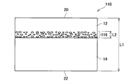
- FIG. 2 The schematic diagram of the laminated board which concerns on Example 2.
- the schematic diagram of the laminated board which concerns on Example 3. FIG.
- the laminate disclosed in the present specification is a laminate of an AlN single crystal layer and an AlN polycrystalline layer.
- Single crystal AlN for example, compared to sapphire is a Al x Ga y N (0 ⁇ x ⁇ 1,0 ⁇ y ⁇ 1) or the same close nitride semiconductor and the lattice constant of such. Therefore, the AlN single crystal layer of the laminated plate disclosed in the present specification is useful as a growth substrate for an ultraviolet light emitting device (UV LED) having a nitride semiconductor as a functional layer. Further, the laminated board disclosed in the present specification is useful as a handling substrate when manufacturing an ultraviolet light emitting device.
- UV LED ultraviolet light emitting device
- the laminate disclosed in the present specification is provided with an AlN polycrystalline layer on the back surface side of the AlN single crystal layer (the side on which the functional layer of the ultraviolet light emitting device is not provided).
- the AlN polycrystalline layer can be obtained (or manufactured) at a relatively low cost. Therefore, by laminating the AlN single crystal layer and the AlN polycrystalline layer, a high-strength growth substrate having a relatively close lattice constant to that of the nitride semiconductor can be realized without using an expensive thick AlN single crystal plate. be able to.
- the laminated board disclosed in the present specification has a void-containing region in which voids are dispersed and introduced at the interface portion between the AlN single crystal layer and the AlN polycrystalline layer.
- the coefficient of thermal expansion of single crystal AlN and the coefficient of thermal expansion of polycrystalline AlN are relatively close but slightly different. Therefore, when the AlN single crystal layer and the AlN polycrystalline layer are laminated, a force may be applied from the AlN polycrystalline layer to the AlN polycrystalline layer at the time of heat treatment or the like based on the difference in the coefficient of thermal expansion between the two. As a result, warpage or cracks may occur in the AlN single crystal layer.
- the laminated board disclosed in the present specification is caused by the difference in thermal expansion coefficient between the AlN single crystal layer and the AlN polycrystalline layer by providing a void-containing region at the interface portion between the AlN single crystal layer and the AlN polycrystalline layer. Therefore, the strain generated at the interface portion can be absorbed. Specifically, the void-containing region is physically deformed, and the force applied to the AlN crystal layer can be relaxed. Therefore, it is possible to reduce the occurrence of warpage and cracks in the AlN single crystal layer.
- the laminated plate disclosed in the present specification is provided with a void-containing region, so that when the AlN polycrystalline layer is removed by mechanical polishing, the impact of the void-containing region on the AlN single crystal layer is reduced. be able to. That is, the void-containing region absorbs the impact generated during mechanical polishing. Therefore, the force (vibration) applied to the functional layer of the ultraviolet light emitting device can be reduced, and the influence on the functional layer can be reduced.
- the laminated board disclosed in the present specification is not particularly limited, but may have a thickness (distance between the front and back surfaces including the AlN single crystal layer and the AlN polycrystalline layer) of 0.5 to 10.0 mm.
- the void-containing region may be provided at a portion in contact with the interface between the AlN single crystal layer and the AlN polycrystalline layer. That is, the void-containing region may be provided in the AlN single crystal layer, may be provided in the AlN polycrystalline layer, or may be provided across both the AlN single crystal layer and the AlN polycrystalline layer. It may have been.
- the thickness of the void-containing region may be 0.1 ⁇ m or more and 5.0 ⁇ m or less. That is, the void-containing region is locally provided in the thickness direction from the front surface to the back surface of the laminated board.
- the thickness of the void-containing region is 0.1 ⁇ m or more, the effect of alleviating the influence of the difference in the coefficient of thermal expansion between the AlN single crystal layer and the AlN polycrystalline layer can be obtained, and the impact generated during mechanical polishing is sufficient. Can be absorbed by.
- the thickness of the void-containing region is sufficiently thinned with respect to the thickness of the laminated plate, so that the thickness that substantially functions as the AlN single crystal layer and the AlN polycrystalline layer is sufficient. It is possible to maintain the mechanical strength of the laminated board.
- the thickness of the void-containing region may be 0.2 ⁇ m or more, 0.3 ⁇ m or more, 0.5 ⁇ m or more, 0.7 ⁇ m or more, and 1.0 ⁇ m or more. It may be 1.5 ⁇ m or more.
- the thickness of the void-containing region may be 4.5 ⁇ m or less, 4.0 ⁇ m or less, 3.5 ⁇ m or less, or 3.0 ⁇ m or less.
- the distance between adjacent voids in the void-containing region may be 1 ⁇ m or more and 300 ⁇ m or less.
- the gap between the voids may be 1 ⁇ m or more and 300 ⁇ m or less. According to such a configuration, if it is 1 ⁇ m or more, it is possible to reduce the defect (deterioration of the AlN single crystal layer 12) caused by the difference in the coefficient of thermal expansion between the AlN single crystal layer and the AlN polycrystalline layer. Further, if it is 300 ⁇ m or less, the distance between the voids becomes sufficiently small, and the mechanical strength of the laminated board can be maintained.
- the "adjacent voids" mean voids adjacent to each other in a direction (substantially parallel) along the end face in the thickness direction of the AlN polycrystalline layer.
- the distance between the voids in the adjacent void-containing regions may be 2 ⁇ m or more, 5 ⁇ m or more, 10 ⁇ m or more, 20 ⁇ m or more, and 25 ⁇ m or more. Further, the distance between the void components in the void content region may be 275 ⁇ m or less, 250 ⁇ m or less, 200 ⁇ m or less, 150 ⁇ m or less, or 100 ⁇ m or less. ..
- the shape of the voids may have an aspect ratio of more than 1 and 10 or less.
- the shape of the void may exist in the void-containing region so that the long side is along the first surface (or the first surface and the second surface) (substantially parallel).
- the long side of the gap may be arranged so as to form an angle of less than 20 degrees with respect to the first surface.
- the aspect ratio of the voids is larger than 1, it is possible to reduce the defect (deterioration of the AlN single crystal layer 12) caused by the difference in the coefficient of thermal expansion between the AlN single crystal layer and the AlN polycrystalline layer.
- the aspect ratio when the aspect ratio is 10 or less, the mechanical strength of the laminated board can be maintained.
- the aspect ratio may be 0.5 or more, 1.0 or more, 1.5 or more, or 2.0 or more. Further, the aspect ratio may be 8 or less, 7 or less, 5 or less, or 3 or less.
- the ratio of voids (void ratio) to the total volume (AlN matrix + voids) may be 1 to 10 vol%.
- the void ratio is 1 vol% or more, the effect of absorbing the strain generated at the above-mentioned interface portion and the effect of absorbing the impact generated during mechanical polishing can be sufficiently obtained. Further, if it is 10 vol% or less, the strength of the laminated board is sufficiently secured. Further, even when the volume of the void is less than 1 vol% with respect to the total volume in the range of 0.1 ⁇ m in the thickness direction with respect to the specific void, the void is different from the void constituting the void-containing region.
- the laminated board disclosed in the present specification may contain a small amount of voids in the AlN single crystal layer or the AlN polycrystalline layer in addition to the void-containing region.
- the ratio of voids in the void-containing region is 1 to 10 vol%, the effect of absorbing the strain generated at the interface portion due to the difference in the coefficient of thermal expansion and the effect of absorbing the impact generated during mechanical polishing are sufficiently exhibited.
- Example 1 Hereinafter, the laminated board 10 according to the embodiment will be described.
- the laminated board 10 is used as a handling substrate for manufacturing the ultraviolet light emitting device 1. Therefore, before explaining the laminated plate 10 in detail, the ultraviolet light emitting device 1 using the laminated plate 10 as a handling substrate will be briefly described.
- the ultraviolet light emitting device 1 is an ultraviolet light emitting diode (UV LED), and includes an AlN single crystal layer 12, an n-type nitride semiconductor layer 2, a p-type nitride semiconductor layer 3, and a light emitting layer 4.
- the n-type nitride semiconductor layer 2 is provided on the surface of the AlN single crystal layer 12.
- the light emitting layer 4 is provided on a part of the surface of the n-type nitride semiconductor layer 2 (on the right side in FIG. 1). Therefore, the surface of the n-type nitride semiconductor layer 2 is partially provided with the light emitting layer 4, and the other parts are exposed.
- a p-type nitride semiconductor layer 3 is provided on the surface of the light emitting layer 4.
- the light emitting layer 4 is provided between the n-type nitride semiconductor layer 2 and the p-type nitride semiconductor layer 3. Electrodes (not shown) are provided on the surface of the p-type nitride semiconductor layer 3 and the exposed portion of the surface of the n-type nitride semiconductor layer 2, respectively.
- the n-type nitride semiconductor layer 2 may actually be formed of a plurality of layers, and the p-type nitride semiconductor layer 3 may be formed of a plurality of layers.
- the light emitting layer 4 may be formed of a plurality of layers.
- each layer of the n-type nitride semiconductor layer 2, each layer of the p-type nitride semiconductor layer 3, and each layer of the light emitting layer 4 can be appropriately selected according to the application of the ultraviolet light emitting device 1.
- the n-type nitride semiconductor layer 2 is formed on the surface of the laminated plate 10 of this embodiment (specifically, the surface of the AlN single crystal layer 12).
- the light emitting layer 4 is formed on the surface of the formed n-type nitride semiconductor layer 2, and the p-type nitride semiconductor layer 3 is formed on the surface of the formed light emitting layer 4.
- a part of the light emitting layer 4 and the p-type nitride semiconductor layer 3 is removed to expose a part of the surface of the n-type nitride semiconductor layer 2.
- the nitride semiconductor layers 2, 3 and 4 are formed on the surface of the laminated plate 10 (the surface of the AlN single crystal layer 12). Further, in order to facilitate the film formation and processing of the n-type nitride semiconductor layer 2, the p-type nitride semiconductor layer 3, and the light emitting layer 4, a thick laminate is used as a handling substrate when manufacturing the ultraviolet light emitting device 1. The plate 10 is used.
- the laminated plate 10 since the AlN single crystal layer 12 and the AlN polycrystalline layer 14 are laminated on the laminated plate 10, if the laminated plate 10 is used as it is as the substrate of the ultraviolet light emitting device 1, the AlN polycrystalline layer 14 emits light ( Ultraviolet light) becomes difficult to pass through the laminated plate 10. Therefore, after the n-type nitride semiconductor layer 2, the p-type nitride semiconductor layer 3, and the light emitting layer 4 are formed, the laminated plate 10 is thinned to a required thickness. That is, the AlN polycrystalline layer 14 which is an unnecessary portion is removed from the laminated plate 10 so that only the AlN single crystal layer 12 required as a substrate is left.
- the n-type nitride semiconductor layer 2, the p-type nitride semiconductor layer 3, and the light emitting layer 4 may be collectively referred to as a “functional layer”.
- the laminated board 10 includes an AlN single crystal layer 12 and an AlN polycrystalline layer 14.
- the AlN single crystal layer 12 is composed of the single crystal AlN.
- the AlN polycrystalline layer 14 is composed of polycrystalline AlN.
- single crystal AlN and polycrystalline AlN are defined as follows. Counting time under the conditions of voltage 40 kV, current 40 mA, collimator diameter 0.5 mm, anti-scattering slit 3 mm, ⁇ step width 0.01 ° using XRD device (D8-DISCOVER manufactured by Bruker-AXS) using CuK ⁇ wire. The XRC profile of the (002) plane of the AlN single crystal layer is measured in 1 second.
- Both the AlN single crystal layer 12 and the AlN polycrystalline layer 14 can be formed by, for example, a sublimation method.
- the method for forming the AlN single crystal layer 12 and the AlN polycrystal layer 14 is not particularly limited, and the AlN single crystal layer 12 and the AlN polycrystal layer 14 are, for example, a CVD method, an HVPE method, an MBE method, or sputtering.
- Use other methods such as vapor phase film formation method such as method, liquid phase film formation method such as hydrothermal method and Na flux method, and room temperature bonding in which single crystal AlN and multicrystal AlN are bonded by surface activation method. Can also be formed.
- the laminated board 10 includes a void-containing region 16 provided between the front surface 20 and the back surface 22.
- the void-containing region 16 is arranged at the interface portion between the AlN single crystal layer 12 and the AlN polycrystalline layer 14 (hereinafter, also simply referred to as “interface portion”), and in this embodiment, the void-containing region 16 is arranged.
- the void-containing region 16 is arranged so as to straddle both the AlN single crystal layer 12 and the AlN polycrystalline layer 14 in the interface portion.
- the ultraviolet light emitting device 1 is manufactured by using the laminated plate 10 as the handling substrate in the laminated plate 10, the surface on which the functional layer is formed (that is, the AlN single crystal layer 12 in the thickness direction) is formed.
- the exposed surface is referred to as the front surface 20, and the surface on the opposite side thereof (that is, the exposed surface of the AlN polycrystalline layer 14 in the thickness direction) is referred to as the back surface 22.
- the void-containing region 16 is locally provided in the thickness direction of the laminated plate 10, and is provided substantially parallel to the back surface 14.
- the void-containing region 16 is arranged across both the AlN single crystal layer 12 and the AlN polycrystalline layer 14 at the interface between the AlN single crystal layer 12 and the AlN polycrystalline layer 14.
- a plurality of voids are dispersed and introduced in the AlN single crystal layer 12 and the AlN polycrystalline layer 14.
- the voids in the void-containing region 16 have an aspect ratio of more than 1 and adjusted to 10 or less, and the long sides are arranged along the front surface 12 and the back surface 14. Further, the voids are arranged at intervals so that the distance between the adjacent voids is 1 ⁇ m to 300 ⁇ m.
- the density of voids (pores) in the void-containing region 16 (ratio of voids to the total volume) is adjusted to 1 to 10 vol%.
- the method of introducing the void into the void-containing region 16 is not particularly limited. For example, when the laminated board 10 is manufactured by a vapor phase growth method such as a sublimation method, the heating temperature of the raw material is raised at the timing of forming the void-containing region 16 or the supply speed of the raw material (raw material gas) is increased. As a result, the film formation rate can be increased, and a layer in which voids have been introduced (void-containing region 16) can be formed.
- the laminated plate 10 is manufactured by room temperature bonding or the like in which single crystal AlN and polycrystalline AlN are joined by a surface activation method, unevenness is intentionally formed on the surface of the polycrystalline AlN and the layers are joined.
- a layer in which voids are introduced (void-containing region 16) can be formed.
- the laminated board 10 of this embodiment includes a void-containing region 16 at an interface portion.
- the strain at the interface portion due to the difference in the coefficient of thermal expansion between the AlN single crystal layer 12 and the AlN polycrystalline layer 14 can be alleviated. Therefore, deterioration of the AlN single crystal layer 12 can be suppressed.
- the ultraviolet light emitting device 1 can be formed on the surface of the high-quality AlN single crystal layer 12, the adverse effect on the functional layer of the ultraviolet light emitting device 1 can be reduced.
- the laminated plate 10 of this embodiment is provided with the void-containing region 16, the impact is absorbed by the voids during mechanical polishing. Therefore, the force (vibration) applied to the functional layer of the ultraviolet light emitting device 1 can be reduced, and the adverse effect on the functional layer can be reduced.
- the thickness L1 of the laminated board 10 is adjusted to 0.5 mm to 10.0 mm, and the thickness L2 of the void-containing region 16 is adjusted to 0.1 ⁇ m to 0.5 ⁇ m.
- the thickness L1 of the laminated plate 10 is the length between the front surface 20 and the back surface 22, and indicates the length in the direction perpendicular to the front surface 20 and the back surface 22.
- the thickness L1 of the laminated plate 10 is the length from the exposed surface of the AlN single crystal layer 12 to the exposed surface of the AlN polycrystalline layer 14 via the interface portion.
- the thickness L2 of the void-containing region 16 also indicates the length in the direction perpendicular to the front surface 20 and the back surface 22.
- the thickness L2 of the void-containing region 16 By setting the thickness L2 of the void-containing region 16 to 0.1 ⁇ m or more, the defect (deterioration of the AlN single crystal layer 12) caused by the difference in the coefficient of thermal expansion between the AlN single crystal layer 12 and the AlN polycrystalline layer 14 is reduced. The effect can be obtained more reliably. Further, by setting the thickness L2 to 0.1 ⁇ m or more, the void-containing region 16 can sufficiently absorb the impact when the laminated plate 10 is mechanically polished. Further, by setting the thickness L2 to 0.5 ⁇ m or less, the ratio of the void-containing region 16 to the total thickness of the laminated board 10 can be reduced.
- the mechanical strength of the AlN layer is lowered.
- the thickness L2 is 0.5 ⁇ m or less, it is possible to suppress a decrease in the mechanical strength of the laminated plate 10, and it is possible to sufficiently secure the mechanical strength of the laminated plate 10.
- Example 2 In Example 1 above, the void-containing region 16 is arranged in both the AlN single crystal layer 12 and the AlN polycrystalline layer 14, but is not limited to such a configuration.
- the void-containing region may be arranged at the interface between the AlN single crystal layer 12 and the AlN polycrystalline layer 14.
- the void-containing region 116 is arranged in the AlN single crystal layer 12. It may have been done.
- the void-containing region 116 is different from the void-containing region 16 of Example 1, and the other configurations are substantially the same. Therefore, the description of the same configuration as that of the laminated board 10 of the first embodiment will be omitted.
- the void-containing region 116 of the laminated plate 110 is arranged in the AlN single crystal layer 12. That is, the voids are introduced into the AlN single crystal layer 12 at the interface portion between the AlN single crystal layer 12 and the AlN polycrystalline layer 14. Since the size and density of the voids introduced into the void-containing region 116 and the thickness L2 of the void-containing region 116 are the same as those of the void-containing region 16 of Example 1, detailed description thereof will be omitted.
- the void-containing region 116 is provided at the interface portion, there is a problem caused by the difference in the coefficient of thermal expansion between the AlN single crystal layer 12 and the AlN polycrystalline layer 14 due to the void-containing region 116. Can be reduced. As a result, deterioration of the AlN single crystal layer 12 can be suppressed. Further, by providing the void-containing region 116, the laminated plate 110 can sufficiently absorb the impact generated when the laminated plate 110 is mechanically polished in order to remove the AlN polycrystalline layer 14.
- the void-containing region may be arranged at the interface portion between the AlN single crystal layer 12 and the AlN polycrystalline layer 14.
- the void-containing region 216 is inside the AlN polycrystalline layer 14. It may be arranged in.
- the void-containing region 216 is different from the void-containing region 16 of Example 1, and the other configurations are substantially the same. Therefore, the description of the same configuration as that of the laminated board 10 of the first embodiment will be omitted.
- the void-containing region 216 of the laminated board 210 is arranged in the AlN polycrystalline layer 14. That is, the voids are introduced into the AlN polycrystalline layer 14 at the interface between the AlN single crystal layer 12 and the AlN polycrystalline layer 14. Since the size and density of the voids introduced into the void-containing region 216 and the thickness L2 of the void-containing region 116 are the same as those of the void-containing region 16 of Example 1, detailed description thereof will be omitted.
- the void-containing region 216 is provided at the interface portion, there is a problem caused by the difference in the coefficient of thermal expansion between the AlN single crystal layer 12 and the AlN polycrystalline layer 14 due to the void-containing region 216. Can be reduced. As a result, deterioration of the AlN single crystal layer 12 can be suppressed. Further, since the laminated plate 210 is provided with the void-containing region 216, it is possible to sufficiently absorb the impact generated when the laminated plate 210 is mechanically polished in order to remove the AlN polycrystalline layer 14.
Landscapes
- Chemical & Material Sciences (AREA)
- Inorganic Chemistry (AREA)
- Engineering & Computer Science (AREA)
- Crystallography & Structural Chemistry (AREA)
- Materials Engineering (AREA)
- Metallurgy (AREA)
- Organic Chemistry (AREA)
- Led Devices (AREA)
- Crystals, And After-Treatments Of Crystals (AREA)
Priority Applications (1)
| Application Number | Priority Date | Filing Date | Title |
|---|---|---|---|
| JP2021567342A JP7700051B2 (ja) | 2019-12-23 | 2020-12-16 | AlN積層板 |
Applications Claiming Priority (2)
| Application Number | Priority Date | Filing Date | Title |
|---|---|---|---|
| JP2019231910 | 2019-12-23 | ||
| JP2019-231910 | 2019-12-23 |
Publications (1)
| Publication Number | Publication Date |
|---|---|
| WO2021131967A1 true WO2021131967A1 (ja) | 2021-07-01 |
Family
ID=76575915
Family Applications (1)
| Application Number | Title | Priority Date | Filing Date |
|---|---|---|---|
| PCT/JP2020/046972 Ceased WO2021131967A1 (ja) | 2019-12-23 | 2020-12-16 | AlN積層板 |
Country Status (2)
| Country | Link |
|---|---|
| JP (1) | JP7700051B2 (https=) |
| WO (1) | WO2021131967A1 (https=) |
Citations (4)
| Publication number | Priority date | Publication date | Assignee | Title |
|---|---|---|---|---|
| JP2009190960A (ja) * | 2008-01-16 | 2009-08-27 | Tokyo Univ Of Agriculture & Technology | 積層体およびその製造方法 |
| JP2010010613A (ja) * | 2008-06-30 | 2010-01-14 | Tokuyama Corp | 積層体、自立基板製造用基板、自立基板およびこれらの製造方法 |
| JP2011020900A (ja) * | 2009-07-16 | 2011-02-03 | Tokuyama Corp | 窒化アルミニウム単結晶層を有する積層体の製造方法、該製法で製造される積層体、該積層体を用いた窒化アルミニウム単結晶基板の製造方法、および、窒化アルミニウム単結晶基板 |
| JP2016175816A (ja) * | 2015-03-23 | 2016-10-06 | Tdk株式会社 | アルミナ基板 |
Family Cites Families (1)
| Publication number | Priority date | Publication date | Assignee | Title |
|---|---|---|---|---|
| JP4565042B1 (ja) | 2009-04-22 | 2010-10-20 | 株式会社トクヤマ | Iii族窒化物結晶基板の製造方法 |
-
2020
- 2020-12-16 WO PCT/JP2020/046972 patent/WO2021131967A1/ja not_active Ceased
- 2020-12-16 JP JP2021567342A patent/JP7700051B2/ja active Active
Patent Citations (4)
| Publication number | Priority date | Publication date | Assignee | Title |
|---|---|---|---|---|
| JP2009190960A (ja) * | 2008-01-16 | 2009-08-27 | Tokyo Univ Of Agriculture & Technology | 積層体およびその製造方法 |
| JP2010010613A (ja) * | 2008-06-30 | 2010-01-14 | Tokuyama Corp | 積層体、自立基板製造用基板、自立基板およびこれらの製造方法 |
| JP2011020900A (ja) * | 2009-07-16 | 2011-02-03 | Tokuyama Corp | 窒化アルミニウム単結晶層を有する積層体の製造方法、該製法で製造される積層体、該積層体を用いた窒化アルミニウム単結晶基板の製造方法、および、窒化アルミニウム単結晶基板 |
| JP2016175816A (ja) * | 2015-03-23 | 2016-10-06 | Tdk株式会社 | アルミナ基板 |
Also Published As
| Publication number | Publication date |
|---|---|
| JP7700051B2 (ja) | 2025-06-30 |
| JPWO2021131967A1 (https=) | 2021-07-01 |
Similar Documents
| Publication | Publication Date | Title |
|---|---|---|
| TWI489016B (zh) | Single crystal substrate, single crystal substrate manufacturing method, multi-layer single-crystal substrate manufacturing method and component manufacturing method | |
| JP5665676B2 (ja) | Iii族窒化物エピタキシャル基板およびその製造方法 | |
| JP6216349B2 (ja) | 層構造の製造方法 | |
| JP2018514498A (ja) | ダイヤモンド−半導体複合基板を製造する方法 | |
| CN107881557B (zh) | 氮化物晶体衬底的制造方法及氮化物晶体层叠体 | |
| CN102272889A (zh) | 电子器件用外延基板及其生产方法 | |
| JP5159858B2 (ja) | 窒化ガリウム系化合物半導体基板とその製造方法 | |
| JP2010251738A (ja) | 窒化物半導体エピタキシャル基板 | |
| JP4907476B2 (ja) | 窒化物半導体単結晶 | |
| KR101227580B1 (ko) | 인장 층의 이완 | |
| JP6138974B2 (ja) | 半導体基板 | |
| JP2020502034A (ja) | 合成ダイヤモンド板 | |
| JP6465785B2 (ja) | 化合物半導体基板 | |
| JP2005209925A5 (https=) | ||
| JP7700051B2 (ja) | AlN積層板 | |
| JP5989559B2 (ja) | 複合基板 | |
| JP2006339308A (ja) | 半導体発光素子 | |
| JP6029538B2 (ja) | 半導体装置 | |
| JP7620571B2 (ja) | AlN積層板 | |
| CN114761630B (zh) | AlN单晶板 | |
| JP7711608B2 (ja) | 窒化物半導体基板の製造方法 | |
| JP2017109877A (ja) | ダイヤモンド基板 | |
| WO2017022647A1 (ja) | ダイヤモンド基板及びダイヤモンド基板の製造方法 | |
| CN110168418A (zh) | 光学部件以及照明装置 | |
| WO2023119916A1 (ja) | 窒化物半導体基板および窒化物半導体基板の製造方法 |
Legal Events
| Date | Code | Title | Description |
|---|---|---|---|
| 121 | Ep: the epo has been informed by wipo that ep was designated in this application |
Ref document number: 20907197 Country of ref document: EP Kind code of ref document: A1 |
|
| ENP | Entry into the national phase |
Ref document number: 2021567342 Country of ref document: JP Kind code of ref document: A |
|
| NENP | Non-entry into the national phase |
Ref country code: DE |
|
| 122 | Ep: pct application non-entry in european phase |
Ref document number: 20907197 Country of ref document: EP Kind code of ref document: A1 |