WO2021111513A1 - Substrat lié et procédé de production de substrat lié - Google Patents
Substrat lié et procédé de production de substrat lié Download PDFInfo
- Publication number
- WO2021111513A1 WO2021111513A1 PCT/JP2019/047139 JP2019047139W WO2021111513A1 WO 2021111513 A1 WO2021111513 A1 WO 2021111513A1 JP 2019047139 W JP2019047139 W JP 2019047139W WO 2021111513 A1 WO2021111513 A1 WO 2021111513A1
- Authority
- WO
- WIPO (PCT)
- Prior art keywords
- particle defect
- copper plate
- ceramic substrate
- defect hole
- substrate
- Prior art date
Links
- 239000000758 substrate Substances 0.000 title claims abstract description 204
- 238000004519 manufacturing process Methods 0.000 title claims description 22
- 230000007547 defect Effects 0.000 claims abstract description 154
- 239000000919 ceramic Substances 0.000 claims abstract description 98
- RYGMFSIKBFXOCR-UHFFFAOYSA-N Copper Chemical compound [Cu] RYGMFSIKBFXOCR-UHFFFAOYSA-N 0.000 claims abstract description 87
- 229910052802 copper Inorganic materials 0.000 claims abstract description 87
- 239000010949 copper Substances 0.000 claims abstract description 87
- 239000002245 particle Substances 0.000 claims description 142
- 229910052581 Si3N4 Inorganic materials 0.000 claims description 77
- HQVNEWCFYHHQES-UHFFFAOYSA-N silicon nitride Chemical compound N12[Si]34N5[Si]62N3[Si]51N64 HQVNEWCFYHHQES-UHFFFAOYSA-N 0.000 claims description 77
- 238000005219 brazing Methods 0.000 claims description 51
- 239000000463 material Substances 0.000 claims description 41
- 239000013067 intermediate product Substances 0.000 claims description 27
- 238000000034 method Methods 0.000 claims description 19
- 230000002950 deficient Effects 0.000 claims description 4
- 238000010438 heat treatment Methods 0.000 claims description 3
- 238000005304 joining Methods 0.000 claims 1
- 230000015556 catabolic process Effects 0.000 abstract description 20
- 229910052751 metal Inorganic materials 0.000 description 63
- 239000002184 metal Substances 0.000 description 63
- 239000000945 filler Substances 0.000 description 11
- 239000000843 powder Substances 0.000 description 10
- 229910052709 silver Inorganic materials 0.000 description 10
- 239000004332 silver Substances 0.000 description 10
- IJGRMHOSHXDMSA-UHFFFAOYSA-N Atomic nitrogen Chemical compound N#N IJGRMHOSHXDMSA-UHFFFAOYSA-N 0.000 description 8
- 239000000155 melt Substances 0.000 description 8
- 238000007731 hot pressing Methods 0.000 description 5
- 239000002994 raw material Substances 0.000 description 5
- 238000001878 scanning electron micrograph Methods 0.000 description 5
- ATJFFYVFTNAWJD-UHFFFAOYSA-N Tin Chemical compound [Sn] ATJFFYVFTNAWJD-UHFFFAOYSA-N 0.000 description 4
- 230000005684 electric field Effects 0.000 description 4
- 229910052738 indium Inorganic materials 0.000 description 4
- APFVFJFRJDLVQX-UHFFFAOYSA-N indium atom Chemical compound [In] APFVFJFRJDLVQX-UHFFFAOYSA-N 0.000 description 4
- 229910052757 nitrogen Inorganic materials 0.000 description 4
- 239000002002 slurry Substances 0.000 description 4
- 229910052718 tin Inorganic materials 0.000 description 4
- XUIMIQQOPSSXEZ-UHFFFAOYSA-N Silicon Chemical compound [Si] XUIMIQQOPSSXEZ-UHFFFAOYSA-N 0.000 description 3
- BQCADISMDOOEFD-UHFFFAOYSA-N Silver Chemical compound [Ag] BQCADISMDOOEFD-UHFFFAOYSA-N 0.000 description 3
- RTAQQCXQSZGOHL-UHFFFAOYSA-N Titanium Chemical compound [Ti] RTAQQCXQSZGOHL-UHFFFAOYSA-N 0.000 description 3
- 238000009826 distribution Methods 0.000 description 3
- 238000007650 screen-printing Methods 0.000 description 3
- 229910052710 silicon Inorganic materials 0.000 description 3
- 239000010703 silicon Substances 0.000 description 3
- 239000010936 titanium Substances 0.000 description 3
- 229910052719 titanium Inorganic materials 0.000 description 3
- QCWXUUIWCKQGHC-UHFFFAOYSA-N Zirconium Chemical compound [Zr] QCWXUUIWCKQGHC-UHFFFAOYSA-N 0.000 description 2
- 239000012752 auxiliary agent Substances 0.000 description 2
- 230000015572 biosynthetic process Effects 0.000 description 2
- 230000000694 effects Effects 0.000 description 2
- 238000007689 inspection Methods 0.000 description 2
- 238000002844 melting Methods 0.000 description 2
- 230000008018 melting Effects 0.000 description 2
- 150000004767 nitrides Chemical class 0.000 description 2
- 239000004065 semiconductor Substances 0.000 description 2
- 238000005245 sintering Methods 0.000 description 2
- 239000002904 solvent Substances 0.000 description 2
- 239000000126 substance Substances 0.000 description 2
- 229910052726 zirconium Inorganic materials 0.000 description 2
- 239000002518 antifoaming agent Substances 0.000 description 1
- 239000011230 binding agent Substances 0.000 description 1
- 150000001875 compounds Chemical class 0.000 description 1
- 239000002270 dispersing agent Substances 0.000 description 1
- 239000006185 dispersion Substances 0.000 description 1
- 238000002474 experimental method Methods 0.000 description 1
- 238000001914 filtration Methods 0.000 description 1
- 150000004678 hydrides Chemical class 0.000 description 1
- 238000009413 insulation Methods 0.000 description 1
- 238000000465 moulding Methods 0.000 description 1
- -1 titanium hydride Chemical compound 0.000 description 1
- 229910000048 titanium hydride Inorganic materials 0.000 description 1
Images


Classifications
-
- C—CHEMISTRY; METALLURGY
- C04—CEMENTS; CONCRETE; ARTIFICIAL STONE; CERAMICS; REFRACTORIES
- C04B—LIME, MAGNESIA; SLAG; CEMENTS; COMPOSITIONS THEREOF, e.g. MORTARS, CONCRETE OR LIKE BUILDING MATERIALS; ARTIFICIAL STONE; CERAMICS; REFRACTORIES; TREATMENT OF NATURAL STONE
- C04B37/00—Joining burned ceramic articles with other burned ceramic articles or other articles by heating
- C04B37/02—Joining burned ceramic articles with other burned ceramic articles or other articles by heating with metallic articles
- C04B37/023—Joining burned ceramic articles with other burned ceramic articles or other articles by heating with metallic articles characterised by the interlayer used
-
- H—ELECTRICITY
- H01—ELECTRIC ELEMENTS
- H01L—SEMICONDUCTOR DEVICES NOT COVERED BY CLASS H10
- H01L23/00—Details of semiconductor or other solid state devices
- H01L23/34—Arrangements for cooling, heating, ventilating or temperature compensation ; Temperature sensing arrangements
- H01L23/36—Selection of materials, or shaping, to facilitate cooling or heating, e.g. heatsinks
- H01L23/373—Cooling facilitated by selection of materials for the device or materials for thermal expansion adaptation, e.g. carbon
- H01L23/3735—Laminates or multilayers, e.g. direct bond copper ceramic substrates
-
- C—CHEMISTRY; METALLURGY
- C04—CEMENTS; CONCRETE; ARTIFICIAL STONE; CERAMICS; REFRACTORIES
- C04B—LIME, MAGNESIA; SLAG; CEMENTS; COMPOSITIONS THEREOF, e.g. MORTARS, CONCRETE OR LIKE BUILDING MATERIALS; ARTIFICIAL STONE; CERAMICS; REFRACTORIES; TREATMENT OF NATURAL STONE
- C04B35/00—Shaped ceramic products characterised by their composition; Ceramics compositions; Processing powders of inorganic compounds preparatory to the manufacturing of ceramic products
- C04B35/515—Shaped ceramic products characterised by their composition; Ceramics compositions; Processing powders of inorganic compounds preparatory to the manufacturing of ceramic products based on non-oxide ceramics
- C04B35/58—Shaped ceramic products characterised by their composition; Ceramics compositions; Processing powders of inorganic compounds preparatory to the manufacturing of ceramic products based on non-oxide ceramics based on borides, nitrides, i.e. nitrides, oxynitrides, carbonitrides or oxycarbonitrides or silicides
- C04B35/584—Shaped ceramic products characterised by their composition; Ceramics compositions; Processing powders of inorganic compounds preparatory to the manufacturing of ceramic products based on non-oxide ceramics based on borides, nitrides, i.e. nitrides, oxynitrides, carbonitrides or oxycarbonitrides or silicides based on silicon nitride
-
- C—CHEMISTRY; METALLURGY
- C04—CEMENTS; CONCRETE; ARTIFICIAL STONE; CERAMICS; REFRACTORIES
- C04B—LIME, MAGNESIA; SLAG; CEMENTS; COMPOSITIONS THEREOF, e.g. MORTARS, CONCRETE OR LIKE BUILDING MATERIALS; ARTIFICIAL STONE; CERAMICS; REFRACTORIES; TREATMENT OF NATURAL STONE
- C04B37/00—Joining burned ceramic articles with other burned ceramic articles or other articles by heating
- C04B37/02—Joining burned ceramic articles with other burned ceramic articles or other articles by heating with metallic articles
- C04B37/023—Joining burned ceramic articles with other burned ceramic articles or other articles by heating with metallic articles characterised by the interlayer used
- C04B37/026—Joining burned ceramic articles with other burned ceramic articles or other articles by heating with metallic articles characterised by the interlayer used consisting of metals or metal salts
-
- H—ELECTRICITY
- H01—ELECTRIC ELEMENTS
- H01L—SEMICONDUCTOR DEVICES NOT COVERED BY CLASS H10
- H01L21/00—Processes or apparatus adapted for the manufacture or treatment of semiconductor or solid state devices or of parts thereof
- H01L21/02—Manufacture or treatment of semiconductor devices or of parts thereof
- H01L21/04—Manufacture or treatment of semiconductor devices or of parts thereof the devices having potential barriers, e.g. a PN junction, depletion layer or carrier concentration layer
- H01L21/48—Manufacture or treatment of parts, e.g. containers, prior to assembly of the devices, using processes not provided for in a single one of the subgroups H01L21/06 - H01L21/326
- H01L21/4814—Conductive parts
- H01L21/4871—Bases, plates or heatsinks
-
- C—CHEMISTRY; METALLURGY
- C04—CEMENTS; CONCRETE; ARTIFICIAL STONE; CERAMICS; REFRACTORIES
- C04B—LIME, MAGNESIA; SLAG; CEMENTS; COMPOSITIONS THEREOF, e.g. MORTARS, CONCRETE OR LIKE BUILDING MATERIALS; ARTIFICIAL STONE; CERAMICS; REFRACTORIES; TREATMENT OF NATURAL STONE
- C04B2237/00—Aspects relating to ceramic laminates or to joining of ceramic articles with other articles by heating
- C04B2237/02—Aspects relating to interlayers, e.g. used to join ceramic articles with other articles by heating
- C04B2237/12—Metallic interlayers
- C04B2237/122—Metallic interlayers based on refractory metals
-
- C—CHEMISTRY; METALLURGY
- C04—CEMENTS; CONCRETE; ARTIFICIAL STONE; CERAMICS; REFRACTORIES
- C04B—LIME, MAGNESIA; SLAG; CEMENTS; COMPOSITIONS THEREOF, e.g. MORTARS, CONCRETE OR LIKE BUILDING MATERIALS; ARTIFICIAL STONE; CERAMICS; REFRACTORIES; TREATMENT OF NATURAL STONE
- C04B2237/00—Aspects relating to ceramic laminates or to joining of ceramic articles with other articles by heating
- C04B2237/02—Aspects relating to interlayers, e.g. used to join ceramic articles with other articles by heating
- C04B2237/12—Metallic interlayers
- C04B2237/124—Metallic interlayers based on copper
-
- C—CHEMISTRY; METALLURGY
- C04—CEMENTS; CONCRETE; ARTIFICIAL STONE; CERAMICS; REFRACTORIES
- C04B—LIME, MAGNESIA; SLAG; CEMENTS; COMPOSITIONS THEREOF, e.g. MORTARS, CONCRETE OR LIKE BUILDING MATERIALS; ARTIFICIAL STONE; CERAMICS; REFRACTORIES; TREATMENT OF NATURAL STONE
- C04B2237/00—Aspects relating to ceramic laminates or to joining of ceramic articles with other articles by heating
- C04B2237/02—Aspects relating to interlayers, e.g. used to join ceramic articles with other articles by heating
- C04B2237/12—Metallic interlayers
- C04B2237/125—Metallic interlayers based on noble metals, e.g. silver
-
- C—CHEMISTRY; METALLURGY
- C04—CEMENTS; CONCRETE; ARTIFICIAL STONE; CERAMICS; REFRACTORIES
- C04B—LIME, MAGNESIA; SLAG; CEMENTS; COMPOSITIONS THEREOF, e.g. MORTARS, CONCRETE OR LIKE BUILDING MATERIALS; ARTIFICIAL STONE; CERAMICS; REFRACTORIES; TREATMENT OF NATURAL STONE
- C04B2237/00—Aspects relating to ceramic laminates or to joining of ceramic articles with other articles by heating
- C04B2237/02—Aspects relating to interlayers, e.g. used to join ceramic articles with other articles by heating
- C04B2237/12—Metallic interlayers
- C04B2237/126—Metallic interlayers wherein the active component for bonding is not the largest fraction of the interlayer
- C04B2237/127—The active component for bonding being a refractory metal
-
- C—CHEMISTRY; METALLURGY
- C04—CEMENTS; CONCRETE; ARTIFICIAL STONE; CERAMICS; REFRACTORIES
- C04B—LIME, MAGNESIA; SLAG; CEMENTS; COMPOSITIONS THEREOF, e.g. MORTARS, CONCRETE OR LIKE BUILDING MATERIALS; ARTIFICIAL STONE; CERAMICS; REFRACTORIES; TREATMENT OF NATURAL STONE
- C04B2237/00—Aspects relating to ceramic laminates or to joining of ceramic articles with other articles by heating
- C04B2237/30—Composition of layers of ceramic laminates or of ceramic or metallic articles to be joined by heating, e.g. Si substrates
- C04B2237/32—Ceramic
- C04B2237/36—Non-oxidic
- C04B2237/368—Silicon nitride
-
- C—CHEMISTRY; METALLURGY
- C04—CEMENTS; CONCRETE; ARTIFICIAL STONE; CERAMICS; REFRACTORIES
- C04B—LIME, MAGNESIA; SLAG; CEMENTS; COMPOSITIONS THEREOF, e.g. MORTARS, CONCRETE OR LIKE BUILDING MATERIALS; ARTIFICIAL STONE; CERAMICS; REFRACTORIES; TREATMENT OF NATURAL STONE
- C04B2237/00—Aspects relating to ceramic laminates or to joining of ceramic articles with other articles by heating
- C04B2237/30—Composition of layers of ceramic laminates or of ceramic or metallic articles to be joined by heating, e.g. Si substrates
- C04B2237/40—Metallic
- C04B2237/407—Copper
-
- H—ELECTRICITY
- H01—ELECTRIC ELEMENTS
- H01L—SEMICONDUCTOR DEVICES NOT COVERED BY CLASS H10
- H01L23/00—Details of semiconductor or other solid state devices
- H01L23/12—Mountings, e.g. non-detachable insulating substrates
- H01L23/14—Mountings, e.g. non-detachable insulating substrates characterised by the material or its electrical properties
- H01L23/15—Ceramic or glass substrates
-
- H—ELECTRICITY
- H05—ELECTRIC TECHNIQUES NOT OTHERWISE PROVIDED FOR
- H05K—PRINTED CIRCUITS; CASINGS OR CONSTRUCTIONAL DETAILS OF ELECTRIC APPARATUS; MANUFACTURE OF ASSEMBLAGES OF ELECTRICAL COMPONENTS
- H05K1/00—Printed circuits
- H05K1/02—Details
- H05K1/03—Use of materials for the substrate
- H05K1/0306—Inorganic insulating substrates, e.g. ceramic, glass
-
- H—ELECTRICITY
- H05—ELECTRIC TECHNIQUES NOT OTHERWISE PROVIDED FOR
- H05K—PRINTED CIRCUITS; CASINGS OR CONSTRUCTIONAL DETAILS OF ELECTRIC APPARATUS; MANUFACTURE OF ASSEMBLAGES OF ELECTRICAL COMPONENTS
- H05K3/00—Apparatus or processes for manufacturing printed circuits
- H05K3/02—Apparatus or processes for manufacturing printed circuits in which the conductive material is applied to the surface of the insulating support and is thereafter removed from such areas of the surface which are not intended for current conducting or shielding
- H05K3/022—Processes for manufacturing precursors of printed circuits, i.e. copper-clad substrates
-
- H—ELECTRICITY
- H05—ELECTRIC TECHNIQUES NOT OTHERWISE PROVIDED FOR
- H05K—PRINTED CIRCUITS; CASINGS OR CONSTRUCTIONAL DETAILS OF ELECTRIC APPARATUS; MANUFACTURE OF ASSEMBLAGES OF ELECTRICAL COMPONENTS
- H05K3/00—Apparatus or processes for manufacturing printed circuits
- H05K3/38—Improvement of the adhesion between the insulating substrate and the metal
Definitions
- the present invention relates to a bonded substrate and a method for manufacturing the bonded substrate.
- Silicon nitride ceramics have high thermal conductivity and high insulation. Therefore, a bonded substrate in which a copper plate is bonded to a silicon nitride ceramic substrate via a bonding layer is suitably used as an insulating heat-dissipating substrate on which a power semiconductor element is mounted.
- dielectric breakdown occurs starting from the end of the copper plate where the electric field is concentrated by applying an electric field that exceeds the withstand voltage of the particles inside the particles constituting the silicon nitride ceramic substrate and the grain boundaries between the particles.
- Mode to do The second mode is a mode in which cracks are formed by partial discharge starting from defects such as voids in the silicon nitride ceramic substrate, and the formed cracks propagate to cause dielectric breakdown starting from the defects. ..
- the dielectric breakdown of the first mode described above can be easily detected by performing a withstand voltage test of the bonded substrate before shipping the bonded substrate. Therefore, it is possible to easily avoid shipping the bonded substrate in which the dielectric breakdown of the first mode described above occurs.
- Defects of the silicon nitride ceramic substrate can be classified into defects isolated inside the silicon nitride ceramic substrate and defects exposed on the surface of the silicon nitride ceramic substrate.
- the defects isolated inside the silicon nitride ceramic substrate are that foreign matter is mixed into the raw material slurry of the silicon nitride ceramic substrate during the production of the silicon nitride ceramic substrate, and the raw material of the silicon nitride ceramic substrate during the production of the silicon nitride ceramic substrate. It is formed by the coarse agglomerates remaining in the raw material slurry due to insufficient dispersion of the raw material powder in the slurry.
- the defects exposed on the surface of the silicon nitride ceramic substrate are that foreign matter adheres to the surface of the intermediate product of the silicon nitride ceramic substrate during the manufacturing of the silicon nitride ceramic substrate, and sintering is performed during the manufacturing of the silicon nitride ceramic substrate. It is formed by volatilizing the auxiliary agent from the surface of the intermediate product of the silicon nitride ceramic substrate during the process.
- the defects isolated inside the silicon nitride ceramic substrate can be easily reduced by filtering the raw material slurry of the silicon nitride ceramic substrate before molding is performed. Therefore, it is possible to easily avoid shipping a bonded substrate in which dielectric breakdown occurs due to partial discharge starting from a defect isolated inside the silicon nitride ceramics.
- partial discharge originating from a defect exposed on the surface of the silicon nitride ceramic substrate cannot be easily found by conducting a withstand voltage test of the bonded substrate before shipping the bonded substrate.
- it is not easy to measure a minute current on the order of pA that flows due to partial discharge and it is not realistic to perform a partial discharge test of the entire bonded substrate to be shipped.
- noise countermeasures must be taken and expensive equipment must be introduced in order to measure the minute current on the order of pA.
- defects exposed on the surface of the silicon nitride ceramic substrate cannot be easily found by performing an image inspection of the silicon nitride ceramic substrate to which the copper plate is not bonded. This is because it is difficult to find a defect that is exposed on the surface of the silicon nitride ceramic substrate and has a diameter of only about 50 ⁇ m and a depth of about 20 ⁇ m. This is because it is not realistic to carry out an inspection. Further, even if it is possible to find a defect having a diameter of only about 50 ⁇ m and a depth of about 20 ⁇ m, expensive equipment must be introduced in order to find the defect. Further, the defects exposed on the surface of the silicon nitride ceramic substrate cannot be easily reduced. Therefore, it cannot be easily avoided to ship a bonded substrate in which dielectric breakdown occurs due to partial discharge starting from a defect exposed on the surface of the silicon nitride ceramics.
- a brazing material pattern is printed on the front and back surfaces of the silicon nitride substrate, and the front and back surfaces of the silicon nitride substrate and the copper plate are joined (paragraph 0029).
- a ceramic substrate having preferable partial discharge characteristics is obtained by controlling the surface morphology of the ceramic substrate by a method that does not introduce defects on the surface as much as possible (paragraph 0038).
- An object to be solved by the present invention is to provide a bonded substrate capable of suppressing the occurrence of dielectric breakdown due to partial discharge starting from a defect exposed on the surface of the ceramic substrate.
- the first aspect of the present invention relates to a bonded substrate.
- the bonding substrate includes a ceramic substrate, a copper plate, and a bonding layer.
- the ceramic substrate has a main surface having a flat region.
- the ceramic substrate has particle defect holes that are exposed on the main surface and impart a flatness lower than the flatness of the flat region to a part of the main surface.
- the copper plate includes a first portion arranged on the flat region and a second portion for filling the particle defect holes.
- the bonding layer includes a third portion that covers the flat region and a fourth portion that fills the particle defect holes. As the bonding layer, a copper plate is bonded to the main surface.
- the second aspect of the present invention relates to a method for manufacturing a bonded substrate.
- the manufacturing method of the bonded substrate includes a step of preparing a ceramic substrate, a step of forming a brazing material layer, and a step of arranging a copper plate on the brazing material layer to obtain an intermediate product having the ceramic substrate, the brazing material layer and the copper plate. It is provided with a process of hot-pressing an intermediate product.
- the ceramic substrate has a main surface having a flat region.
- the ceramic substrate has particle defect holes that are exposed on the main surface and impart a flatness lower than the flatness of the flat region to a part of the main surface.
- a part of the copper plate is made to penetrate into the particle defect hole.
- the copper plate is changed into a copper plate including a first portion arranged on the flat region and a second portion for filling the particle defect hole.
- a part of the brazing filler metal layer is made to penetrate into the particle defect hole.
- the brazing filler metal layer is transformed into a bonding layer that includes a third portion that covers the flat region and a fourth portion that fills the particle defect holes, and joins the copper plate to the main surface.
- the particle defect holes exposed on the main surface of the ceramic substrate constituting the bonding substrate are filled with a part of the copper plate and a part of the bonding layer. Therefore, it is possible to suppress the occurrence of partial discharge starting from the particle defect hole. This makes it possible to provide a bonded substrate capable of suppressing the occurrence of dielectric breakdown due to partial discharge starting from a defect exposed on the surface of the ceramic substrate.
- FIG. 5 is an enlarged cross-sectional view schematically showing a part of a bonding substrate to be compared with the bonding substrate of the first embodiment.
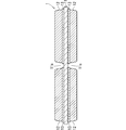
- FIG. 1 is a cross-sectional view schematically showing the bonded substrate of the first embodiment.
- the bonding substrate 1 of the first embodiment shown in FIG. 1 includes a silicon nitride ceramic substrate 11, a copper plate 12, and a bonding layer 13.
- the silicon nitride ceramic substrate 11 may be replaced with a ceramic substrate other than the silicon nitride ceramic substrate.
- the bonding substrate 1 may include elements other than these elements.
- the copper plate 12 and the bonding layer 13 are arranged on the main surface 11s of the silicon nitride ceramic substrate 11.
- the bonding layer 13 joins the copper plate 12 to the main surface 11s of the silicon nitride ceramic substrate 11.
- the bonding substrate 1 may be used in any way, and is used, for example, as an insulated heat-dissipating substrate on which a power semiconductor element is mounted.
- FIG. 2 is an enlarged cross-sectional view schematically showing a part of the bonding substrate of the first embodiment.
- the main surface 11s of the silicon nitride ceramic substrate 11 has a flat region 11f.
- the flat region 11f is a region having high flatness, preferably a region having a maximum height Rz of 10 ⁇ m or less.
- the maximum height Rz is the maximum height when the reference length is 0.8 mm.
- the silicon nitride ceramic substrate 11 has a particle defect hole 11h.
- the particle defect hole 11h is exposed on the main surface 11s of the silicon nitride ceramic substrate 11 and imparts a flatness lower than the flatness of the flat region 11f to a part of the main surface 11s of the silicon nitride ceramic substrate 11. Therefore, the particle defect hole 11h has a depth larger than the maximum height Rz of the flat region 11f.
- foreign matter adheres to the main surface of the intermediate product of the silicon nitride ceramic substrate 11 during the manufacturing of the silicon nitride ceramic substrate 11, and sintering is performed during the manufacturing of the silicon nitride ceramic substrate 11. It is formed by volatilizing an auxiliary agent from the main surface of the intermediate product of the silicon nitride ceramic substrate 11 during the process.
- the copper plate 12 includes a first portion 121 arranged on the flat region 11f of the silicon nitride ceramic substrate 11 and a second portion 122 for filling the particle defect hole 11h.
- the second portion 122 is continuous with the first portion 121 and is electrically connected to the first portion 121.
- the bonding layer 13 includes a third portion 131 that covers the flat region 11f and a fourth portion 132 that fills the particle defect hole 11h.
- the second portion 122 of the copper plate 12 and the fourth portion 132 of the bonding layer 13 fill the particle defect hole 11h. Therefore, in the bonding substrate 1, dielectric breakdown may occur starting from the second portion 122 of the copper plate 12 and the fourth portion 132 of the bonding layer 13 due to the application of an electric field.
- the dielectric breakdown can be found by performing a withstand voltage test on the bonding substrate 1 before shipping the bonding substrate 1. That is, the shipment of the bonding substrate 1 that does not meet the required withstand voltage specifications due to the dielectric breakdown can be suppressed by performing the withstanding voltage test of the bonding substrate 1 before shipping the bonding substrate 1.
- the second portion 122 of the copper plate 12 and the fourth portion 132 of the bonding layer 13 fill the particle defect hole 11h. Therefore, in the bonding substrate 1, it is possible to prevent the particle defect hole 11h from becoming the starting point of partial discharge. As a result, in the bonding substrate 1, it is possible to suppress the formation of cracks due to partial discharge starting from the particle defect hole 11h. Therefore, in the bonding substrate 1, it is possible to suppress the occurrence of dielectric breakdown starting from the particle defect hole 11h due to the growth of cracks formed by the partial discharge starting from the particle defect hole 11h.
- Defects caused by dielectric breakdown occurring starting from the particle defect hole 11h due to the growth of cracks formed by partial discharge starting from 11h are the resistance of the bonding substrate 1 before the bonding substrate 1 is shipped. It is possible to suppress the occurrence after the voltage test is performed.
- the particle defect hole 11h preferably has a depth of 60 ⁇ m or less.
- a dent may be formed on the upper main surface of the copper plate 12 when the second portion 122 of the copper plate 12 is formed.
- cracks may be formed in the silicon nitride ceramic substrate 11 when the copper plate 12 is bonded to the silicon nitride ceramic substrate 11.
- the particle defect hole 11h more preferably has a depth of 30 ⁇ m or less.
- the bonding substrate 1 has particles even when the second portion 122 of the copper plate 12 and the fourth portion 132 of the bonding layer 13 fill the particle defect hole 11h. It has a withstand voltage equivalent to that of a bonded substrate having no defective hole 11h.
- the particle defect hole 11h may have a depth deeper than 30 ⁇ m.
- the withstand voltage of the bonding substrate 1 when the second portion 122 of the copper plate 12 and the fourth portion 132 of the bonding layer 13 fill the particle defect hole 11h.
- it is lower than the withstand voltage of the bonded substrate having no particle defect hole 11h.
- the crack formed by the partial discharge starting from the particle defect hole 11h grows. Defects caused by dielectric breakdown occurring starting from the particle defect hole 11h can be suppressed.
- the second portion 122 of the copper plate 12 and the fourth portion 132 of the bonding layer 13 fill the entire particle defect hole 11h.
- the particle defect hole 11h is the starting point of the partial discharge. Can be suppressed.
- the second portion 122 of the copper plate 12 and the fourth portion 132 of the bonding layer 13 only fill a part of the particle defect hole 11h
- the second portion 122 of the copper plate 12 and the fourth portion 132 of the bonding layer 13 The portion 132 preferably fills 80% or more of the volume of the particle defect hole 11h, and more preferably 90% or more of the volume of the particle defect hole 11h.
- the fourth portion 132 of the bonding layer 13 covers the inner surface 11i of the particle defect hole 11h. This makes it possible to allow the second portion 122 of the copper plate 12 above the fourth portion 132 of the bonding layer 13 to penetrate the inside of the particle defect hole 11h.
- the fourth portion 132 of the bonding layer 13 covers the entire inner surface 11i of the particle defect hole 11h. However, even when the fourth portion 132 of the bonding layer 13 covers only a part of the inner surface 11i of the particle defect hole 11h, the second portion of the copper plate 12 on the fourth portion 132 of the bonding layer 13 It is possible to allow the portion 122 to enter the inside of the particle defect hole 11h. If the fourth portion 132 of the junction layer 13 covers only a portion of the inner surface 11i of the particle defect hole 11h, then the fourth portion 132 of the junction layer 13 is preferably the inner surface 11i of the particle defect hole 11h. It covers 80% or more of the area, and more preferably 90% or more of the area of the inner surface 11i of the particle defect hole 11h.
- the copper plate 12 is bonded to the silicon nitride ceramic substrate 11 via the bonding layer 13.
- the bonding layer 13 is generated from a brazing material layer containing an active metal, and contains an active metal contained in the brazing material layer as a material component.
- the active metal contained in the bonding layer 13 is at least one active metal selected from the group consisting of titanium and zirconium.
- the bonding layer 13 may contain a metal other than the active metal.
- the metal other than the active metal contained in the bonding layer 13 is at least one metal selected from the group consisting of silver, copper, indium and tin.
- the bonding layer 13 may contain nitrogen and / or silicon supplied from the silicon nitride ceramic substrate 11. The supplied nitrogen and / or silicon may form a compound with the active metal.
- the bonding layer 13 may include copper supplied from the copper plate 12.
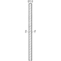
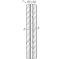
- FIG. 3 is a flowchart illustrating the flow of manufacturing of the bonded substrate of the first embodiment.
- 4, 5 and 6 are cross-sectional views schematically illustrating an intermediate product obtained in the process of manufacturing the bonded substrate of the first embodiment.
- steps S101 to S105 shown in FIG. 3 are sequentially executed.
- step S101 the silicon nitride ceramic substrate 11 is prepared.
- the silicon nitride ceramic substrate 11 to be prepared has a main surface 11s and has a particle defect hole 11h exposed on the main surface 11s.
- step S102 as shown in FIG. 4, the brazing filler metal layer 13i is formed on the main surface 11s of the silicon nitride ceramic substrate 11.
- a paste containing an active metal brazing filler metal and a solvent is prepared.
- the paste may further contain a binder, a dispersant, an antifoaming agent and the like.
- the prepared paste is screen-printed on the main surface 11s of the silicon nitride ceramic substrate 11, and a screen printing film is formed on the main surface 11s of the silicon nitride ceramic substrate 11.
- the solvent contained in the formed screen printing film is volatilized.
- the screen printing film changes to the brazing material layer 13i.
- the brazing filler metal layer 13i contains an active metal brazing filler metal.
- the brazing filler metal layer 13i may be formed by a method different from this method.
- the active metal brazing material includes hydrogenated active metal powder and metal powder.
- the hydrogenated active metal powder contains a hydride of at least one active metal selected from the group consisting of titanium and zirconium.
- the metal powder contains silver.
- the metal powder may contain a metal other than silver.
- the metal other than silver is at least one metal selected from the group consisting of copper, indium and tin.
- the melting point of the active metal brazing material is lower than the melting point of silver.
- the active metal brazing material preferably contains 40% by weight or more and 80% by weight or less of silver.
- the active metal brazing material preferably consists of a powder having an average particle size of 0.1 ⁇ m or more and 10 ⁇ m or less.
- the average particle size can be obtained by measuring the particle size distribution with a commercially available laser diffraction type particle size distribution measuring device and calculating the median diameter D50 from the measured particle size distribution. Since the active metal brazing material is composed of a powder having such a small average particle size, the brazing material layer 13i can be thinned.
- the brazing filler metal layer 13i preferably has a thickness of 0.1 ⁇ m or more and 10 ⁇ m or less, and more preferably 0.1 ⁇ m or more and 5 ⁇ m or less.
- step S103 as shown in FIG. 5, the copper plate 12i is arranged on the formed brazing material layer 13i.
- an intermediate product 1i including the silicon nitride ceramic substrate 11, the copper plate 12i, and the brazing material layer 13i can be obtained.
- step S104 hot pressing is performed on the obtained intermediate product 1i. While the hot press is being performed, the active metal contained in the brazing material layer 13i reacts with the nitrogen contained in the silicon nitride ceramic substrate 11. This produces a nitride of the active metal. Further, the melt of the active metal brazing material gets wet with the generated nitride of the active metal. Further, the molten metal brazing material gets wet with the copper plate 12i. The substance constituting the melt of the active metal brazing material is combined with the substance constituting the silicon nitride ceramic substrate 11 and the copper plate 12i, and the copper plate 12j and the silicon nitride ceramic substrate 11 are joined to each other as shown in FIG. The bonding layer 13j to be formed is formed.
- the bonding layer 13j includes a third portion 131 that covers the flat region 11f and a fourth portion 132 that fills the particle defect hole 11h.
- the copper plate 12i changes to a copper plate 12j as shown in FIG. When the copper plate 12i changes to the copper plate 12j, a part of the copper plate 12i penetrates into the particle defect hole 11h exposed on the main surface 11s of the silicon nitride ceramic substrate 11.
- the copper plate 12j includes a first portion 121 arranged on the flat region 11f and a second portion 122 that fills the particle defect hole 11h.
- an intermediate product 1j including a silicon nitride ceramic substrate 11, a copper plate 12j, and a bonding layer 13j can be obtained.
- the intermediate product 1i When hot pressing is performed on the intermediate product 1i, it is desirable that the intermediate product 1i is in the thickness direction of the silicon nitride ceramic substrate 11 according to the surface pressure profile having the maximum surface pressure of 5 MPa or more and 30 MPa or less in vacuum. It is heated according to a temperature profile having a maximum temperature of 800 ° C. or higher and 900 ° C. or lower while being pressurized to. As a result, the copper plate 12i can be bonded to the silicon nitride ceramic substrate 11 even when the brazing material layer 13i has a thin thickness of 0.1 ⁇ m or more and 10 ⁇ m or less.
- FIG. 8 is an enlarged cross-sectional view schematically showing a part of the bonding substrate to be compared with the bonding substrate of the first embodiment.
- the melt of the active metal brazing material has good wettability with respect to the copper plate 12i. Therefore, the melt of the active metal brazing material existing on the particle defect hole 11h tends to adhere to the copper plate 12i. Further, the melt of the active metal brazing material existing on the particle defect hole 11h is likely to be drawn into the melt of the active metal brazing material existing on the particle defect hole 11h. Therefore, the melt of the active metal brazing material existing on the particle defect hole 11h does not easily penetrate into the particle defect hole 11h.
- the space filling rate of the powder is about 50% to 60%.
- the melt of the active metal brazing material can fill only about 50% to 60% of the particle defect hole 11h, and voids are formed. It is formed. From these facts, unless the intermediate product 1i is pressed with a sufficient surface pressure and the active metal brazing material is pushed into the particle defect hole 11h, as shown in FIG. 8, the particle defect hole 11h is filled and the particle defect is formed.
- the fourth portion 132 that covers the inner surface 11i of the hole 11h cannot be formed in the bonding layer 13j, and the second portion 122 that fills the particle-deficient hole 11h cannot be formed in the copper plate 12j.
- brazing filler metal layer 13i Even if all or part of silver, copper, indium and tin contained in the brazing filler metal layer 13i is diffused into the silicon nitride ceramic substrate 11 and / or the copper plate 12i while the intermediate product 1i is hot-pressed. Good. Nitrogen and / or silicon contained in the silicon nitride ceramic substrate 11 may be diffused into the brazing filler metal layer 13i while the intermediate product 1i is hot-pressed. The copper contained in the copper plate 12i may be diffused into the brazing material layer 13i.
- step S105 the copper plate 12j and the bonding layer 13j are patterned.
- the copper plate 12i is transformed into the patterned copper plate 12 shown in FIG.
- the bonding layer 13j changes to the patterned bonding layer 13 shown in FIG.
- the bonding substrate 1 was manufactured according to the manufacturing method of the bonding substrate 1 described above.
- As the hydrogenated active metal contained in the active metal brazing material titanium hydride was used.
- As the metal other than the active metal contained in the active metal brazing material silver was used.
- the hot press presses the intermediate product 1i in the thickness direction of the silicon nitride ceramic substrate 11 according to the surface pressure profile having the maximum surface pressure shown in Table 1, and according to the temperature profile having the maximum temperature shown in Table 1. This was done by heating the intermediate product 1i.
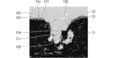
- the cross section of the manufactured bonding substrate 1 was observed with an electron microscope (SEM) to obtain an SEM image.
- SEM electron microscope
- Table 1 shows the internal state of the particle defect hole 11h.
- the fact that the internal state of the particle defect hole 11h is “ ⁇ ” means that 80% or more of the area of the inner surface 11i of the particle defect hole 11h is covered with the fourth portion 132 of the bonding layer 13, and the particles. More than 80% of the volume of the defective hole 11h is filled with the second portion 122 of the copper plate 12 and the fourth portion 132 of the bonding layer 13, indicating that the silicon nitride ceramic substrate 11 is not cracked.
- the internal state of the particle defect hole 11h is “ ⁇ *”, which means that 80% or more of the area of the inner surface 11i of the particle defect hole 11h is covered with the fourth portion 132 of the bonding layer 13. Although 80% or more of the volume of the particle defect hole 11h is filled with the second portion 122 of the copper plate 12 and the fourth portion 132 of the bonding layer 13, cracks are formed in the silicon nitride ceramic substrate 11. Shown. In Table 1, the fact that the internal state of the particle defect hole 11h is “x” means that only 70% or less of the area of the inner surface 11i of the particle defect hole 11h is covered by the fourth portion 132 of the bonding layer 13.
- FIG. 7 shows an SEM image when the maximum surface pressure is 20 MPa and the maximum temperature is 830 ° C.
- the maximum surface pressure is 5 MPa or more and 30 MPa or less and the maximum temperature is 800 ° C. or more and 900 ° C. or less, as shown in Table 1, 80% or more of the area of the inner surface 11i of the particle defect hole 11h is the bonding layer 13.
- the silicon nitride ceramic substrate is covered with the fourth portion 132, and 80% or more of the volume of the particle defect hole 11h is filled with the second portion 122 of the copper plate 12 and the fourth portion 132 of the bonding layer 13. No crack was formed in 11.
- 80% or more of the area of the inner surface 11i of the particle defect hole 11h is the fourth of the bonding layer 13. 80% or more of the volume of the particle defect hole 11h can be filled by the second portion 122 of the copper plate 12 and the fourth portion 132 of the bonding layer 13, and the bonding substrate 1 can be cracked. Can be understood that can be prevented from forming.
- the bonding substrate 1 was manufactured according to the manufacturing method of the bonding substrate 1 described above.
- the silicon nitride ceramic substrate 11 As the silicon nitride ceramic substrate 11, the silicon nitride ceramic substrate 11 having the particle defect holes 11h having the maximum depth shown in Table 2 was used. Titanium was used as the active metal contained in the active metal brazing material. As the metal other than the active metal contained in the active metal brazing material, silver was used.
- the hot press pressurizes the intermediate product 1i in the thickness direction of the silicon nitride ceramic substrate 11 according to the surface pressure profile having the maximum surface pressure shown in Table 2, and the intermediate product 1i according to the temperature profile having the maximum temperature of 830 ° C. Was performed by heating.
- the cross section of the manufactured bonding substrate 1 was observed by SEM to obtain an SEM image.
- the internal state of the particle defect hole 11h was confirmed with reference to the obtained SEM image.
- the maximum surface pressure was 20 MPa
- 90% of the volume of the particle defect hole 11h was filled with the second portion 122 of the copper plate 12 and the fourth portion 132 of the bonding layer 13.
- 70% of the volume of the particle defect hole 11h was filled with the second portion 122 of the copper plate 12 and the fourth portion 132 of the bonding layer 13.
- the withstand voltage test of the manufactured bonding substrate 1 was performed, and the withstand voltage of the bonding substrate 1 in which dielectric breakdown occurs in the bonding substrate 1 was measured.
- Table 2 shows the measured withstand voltage of the bonding substrate 1.
- a partial discharge test of the manufactured bonding substrate 1 was performed, and the partial discharge voltage of the bonding substrate 1 at which the amount of discharge charge reached 10 pC was measured.
- the partial discharge voltage of the bonding substrate 1 was measured by a partial discharge test system manufactured by Soken Electric Co., Ltd. Table 2 shows the measured partial discharge voltage of the bonding substrate 1. When the partial discharge voltage of the bonding substrate 1 was 7 kV or less, it was evaluated that no partial discharge was generated in the bonding substrate 1. Further, when the partial discharge voltage of the bonding substrate 1 was higher than 7 kV, it was evaluated that the bonding substrate 1 was partially discharged.
- the withstand voltage of the bonding substrate 1 is such that the maximum depth of the particle defect hole 11h is 30 ⁇ m. When it was less than or equal to, it was 8 kV, and when the maximum depth of the particle defect hole 11h was deeper than 30 ⁇ m, it was 5 kV.
- the partial discharge voltage of the bonding substrate 1 is the maximum depth of the particle defect hole 11h as shown in Table 2. It was 7 kV regardless of whether the value was 30 ⁇ m or less.
- the withstand voltage of the bonding substrate 1 is such that the maximum depth of the particle defect hole 11h is 30 ⁇ m. When it was less than or equal to, it was 8 kV, and when the maximum depth of the particle defect hole 11h was deeper than 30 ⁇ m, it was 7 kV.
- the partial discharge voltage of the bonding substrate 1 is the maximum depth of the particle defect hole 11h as shown in Table 2. It is 7 kV when the value is 10 ⁇ m or less, 5 kV when the maximum depth of the particle defect hole 11h is deeper than 10 ⁇ m and 20 ⁇ m or less, and 4 kV when the maximum depth of the particle defect hole 11h is deeper than 20 ⁇ m and 30 ⁇ m or less. When the maximum depth of the particle defect hole 11h was deeper than 30 ⁇ m, it was 5 kV.
- the withstand voltage becomes higher than the withstand voltage when 79% of the volume of the particle defect hole 11h is filled, but the partial discharge voltage is particle defect. It becomes lower than the partial discharge voltage when 79% of the volume of the hole 11h is filled, and partial discharge is likely to occur in the bonded substrate 1.
Landscapes
- Engineering & Computer Science (AREA)
- Chemical & Material Sciences (AREA)
- Ceramic Engineering (AREA)
- Microelectronics & Electronic Packaging (AREA)
- Materials Engineering (AREA)
- Power Engineering (AREA)
- Physics & Mathematics (AREA)
- Condensed Matter Physics & Semiconductors (AREA)
- General Physics & Mathematics (AREA)
- Computer Hardware Design (AREA)
- Structural Engineering (AREA)
- Organic Chemistry (AREA)
- Manufacturing & Machinery (AREA)
- Inorganic Chemistry (AREA)
- Manufacturing Of Printed Wiring (AREA)
- Ceramic Products (AREA)
Abstract
L'invention concerne un substrat lié dans lequel la survenue d'une rupture diélectrique provoquée par une décharge partielle provenant d'un défaut exposé sur la surface d'un substrat en céramique peut être supprimée. Le substrat lié comprend un substrat en céramique de nitrure de silicium, une plaque de cuivre et une couche de liaison. Le substrat en céramique comprend une surface principale ayant une région plate. Le substrat céramique a un trou de grain manquant exposé sur la surface principale et conférant à une partie de la surface principale une planéité inférieure à la planéité de la région plate. La plaque de cuivre comprend une première section disposée sur la région plate et une seconde section remplie dans le trou de grain manquant. La couche de liaison comprend une troisième section recouvrant la région plate et une quatrième section remplie dans le trou de grain manquant. La couche de liaison lie la plaque de cuivre à la surface principale.
Priority Applications (7)
| Application Number | Priority Date | Filing Date | Title |
|---|---|---|---|
| PCT/JP2019/047139 WO2021111513A1 (fr) | 2019-12-03 | 2019-12-03 | Substrat lié et procédé de production de substrat lié |
| EP20897100.2A EP4071129A4 (fr) | 2019-12-03 | 2020-11-30 | Substrat lié et procédé de production de substrat lié |
| CN202311466354.0A CN117586041A (zh) | 2019-12-03 | 2020-11-30 | 接合基板以及接合基板的制造方法 |
| CN202080074175.0A CN114599625A (zh) | 2019-12-03 | 2020-11-30 | 接合基板以及接合基板的制造方法 |
| JP2021562631A JP7373585B2 (ja) | 2019-12-03 | 2020-11-30 | 接合基板 |
| PCT/JP2020/044459 WO2021112029A1 (fr) | 2019-12-03 | 2020-11-30 | Substrat lié et procédé de production de substrat lié |
| US17/752,935 US20220285237A1 (en) | 2019-12-03 | 2022-05-25 | Bonded substrate, and bonded substrate manufacturing method |
Applications Claiming Priority (1)
| Application Number | Priority Date | Filing Date | Title |
|---|---|---|---|
| PCT/JP2019/047139 WO2021111513A1 (fr) | 2019-12-03 | 2019-12-03 | Substrat lié et procédé de production de substrat lié |
Publications (1)
| Publication Number | Publication Date |
|---|---|
| WO2021111513A1 true WO2021111513A1 (fr) | 2021-06-10 |
Family
ID=76221557
Family Applications (2)
| Application Number | Title | Priority Date | Filing Date |
|---|---|---|---|
| PCT/JP2019/047139 WO2021111513A1 (fr) | 2019-12-03 | 2019-12-03 | Substrat lié et procédé de production de substrat lié |
| PCT/JP2020/044459 WO2021112029A1 (fr) | 2019-12-03 | 2020-11-30 | Substrat lié et procédé de production de substrat lié |
Family Applications After (1)
| Application Number | Title | Priority Date | Filing Date |
|---|---|---|---|
| PCT/JP2020/044459 WO2021112029A1 (fr) | 2019-12-03 | 2020-11-30 | Substrat lié et procédé de production de substrat lié |
Country Status (5)
| Country | Link |
|---|---|
| US (1) | US20220285237A1 (fr) |
| EP (1) | EP4071129A4 (fr) |
| JP (1) | JP7373585B2 (fr) |
| CN (2) | CN117586041A (fr) |
| WO (2) | WO2021111513A1 (fr) |
Citations (5)
| Publication number | Priority date | Publication date | Assignee | Title |
|---|---|---|---|---|
| JPH08501500A (ja) * | 1992-09-17 | 1996-02-20 | エー. リットランド,マーカス | セラミック−金属複合材の製造方法 |
| JP2013159536A (ja) * | 2012-02-08 | 2013-08-19 | Mino Ceramic Co Ltd | セラミックス多孔体−金属断熱材及びその製造方法 |
| WO2014148534A1 (fr) * | 2013-03-19 | 2014-09-25 | 日本碍子株式会社 | Corps assemblé et procédé de fabrication correspondant |
| JP2014201483A (ja) * | 2013-04-04 | 2014-10-27 | パナソニック株式会社 | セラミックス接合体、電磁継電器およびセラミックス接合体の製造方法 |
| JP2018506496A (ja) * | 2015-12-28 | 2018-03-08 | 日本碍子株式会社 | 接合基板および接合基板の製造方法 |
Family Cites Families (7)
| Publication number | Priority date | Publication date | Assignee | Title |
|---|---|---|---|---|
| JPS6288392A (ja) * | 1985-10-15 | 1987-04-22 | 日本電気株式会社 | セラミツク基板 |
| JP2623250B2 (ja) * | 1987-06-16 | 1997-06-25 | 住友大阪セメント株式会社 | アルミナセラミックと鉄・ニッケル系合金との接合体 |
| JP2000236052A (ja) * | 1999-02-15 | 2000-08-29 | Fuji Electric Co Ltd | 半導体装置用基板およびその製造方法 |
| JP4688380B2 (ja) * | 2001-09-26 | 2011-05-25 | 京セラ株式会社 | 回路基板及びその製造方法 |
| JP2007242815A (ja) * | 2006-03-07 | 2007-09-20 | Eudyna Devices Inc | 配線基板および電子装置並びにその製造方法 |
| JP5499374B2 (ja) | 2008-09-24 | 2014-05-21 | 日立金属株式会社 | 窒化珪素回路基板およびそれを用いた半導体モジュール |
| US10016956B2 (en) * | 2013-09-30 | 2018-07-10 | Mitsubishi Materials Corporation | Cu/ceramic bonded body, method for manufacturing Cu/ceramic bonded body, and power module substrate |
-
2019
- 2019-12-03 WO PCT/JP2019/047139 patent/WO2021111513A1/fr active Application Filing
-
2020
- 2020-11-30 JP JP2021562631A patent/JP7373585B2/ja active Active
- 2020-11-30 EP EP20897100.2A patent/EP4071129A4/fr active Pending
- 2020-11-30 WO PCT/JP2020/044459 patent/WO2021112029A1/fr unknown
- 2020-11-30 CN CN202311466354.0A patent/CN117586041A/zh active Pending
- 2020-11-30 CN CN202080074175.0A patent/CN114599625A/zh active Pending
-
2022
- 2022-05-25 US US17/752,935 patent/US20220285237A1/en active Pending
Patent Citations (5)
| Publication number | Priority date | Publication date | Assignee | Title |
|---|---|---|---|---|
| JPH08501500A (ja) * | 1992-09-17 | 1996-02-20 | エー. リットランド,マーカス | セラミック−金属複合材の製造方法 |
| JP2013159536A (ja) * | 2012-02-08 | 2013-08-19 | Mino Ceramic Co Ltd | セラミックス多孔体−金属断熱材及びその製造方法 |
| WO2014148534A1 (fr) * | 2013-03-19 | 2014-09-25 | 日本碍子株式会社 | Corps assemblé et procédé de fabrication correspondant |
| JP2014201483A (ja) * | 2013-04-04 | 2014-10-27 | パナソニック株式会社 | セラミックス接合体、電磁継電器およびセラミックス接合体の製造方法 |
| JP2018506496A (ja) * | 2015-12-28 | 2018-03-08 | 日本碍子株式会社 | 接合基板および接合基板の製造方法 |
Also Published As
| Publication number | Publication date |
|---|---|
| US20220285237A1 (en) | 2022-09-08 |
| JP7373585B2 (ja) | 2023-11-02 |
| JPWO2021112029A1 (fr) | 2021-06-10 |
| EP4071129A4 (fr) | 2023-11-15 |
| EP4071129A1 (fr) | 2022-10-12 |
| CN114599625A (zh) | 2022-06-07 |
| WO2021112029A1 (fr) | 2021-06-10 |
| CN117586041A (zh) | 2024-02-23 |
Similar Documents
| Publication | Publication Date | Title |
|---|---|---|
| KR100567265B1 (ko) | 적층형 전자부품 | |
| JP5673847B2 (ja) | 窒化珪素基板および窒化珪素基板の製造方法 | |
| JPWO2007083811A1 (ja) | 導体ペースト、多層セラミック基板及び多層セラミック基板の製造方法 | |
| US20130050896A1 (en) | Multilayer ceramic electronic component and method of fabricating the same | |
| JP6609622B2 (ja) | 配線基板 | |
| JP3956136B2 (ja) | 積層型インダクタの製造方法 | |
| WO2021111513A1 (fr) | Substrat lié et procédé de production de substrat lié | |
| JP2016058417A (ja) | 半導体パワーモジュールの製造方法 | |
| CN110692110B (zh) | 导体形成用组合物及其制造方法,导体及其制造方法,芯片电阻器 | |
| WO2020183701A1 (fr) | Substrat lié | |
| US20220285238A1 (en) | Bonded substrate and bonded substrate manufacturing method | |
| KR20190111083A (ko) | 관통 구멍을 밀봉하기 위한 구조 및 방법, 그리고, 관통 구멍을 밀봉하기 위한 전사 기판 | |
| WO2020184510A1 (fr) | Substrat assemblé et procédé de production de substrat assemblé | |
| JP2016058415A (ja) | 半導体パワーモジュールの製造方法 | |
| JP4600553B2 (ja) | ガスセンサの製造方法 | |
| JP6123410B2 (ja) | セラミックス回路基板の製造方法 | |
| TW202242910A (zh) | 接合構造體 | |
| JP4895653B2 (ja) | 電子部品の製造方法 | |
| JP6845090B2 (ja) | セラミック配線基板及びその製造方法 | |
| JP5268847B2 (ja) | 配線基板およびその製造方法 | |
| JP2007221115A (ja) | 導体ペースト及び多層セラミック基板の製造方法 | |
| CN108029203B (zh) | 陶瓷多层基板 | |
| JP7100778B1 (ja) | 静電チャック用給電部及び静電チャック | |
| JP2005209681A (ja) | 導電性ペーストおよび積層セラミック電子部品の製造方法 | |
| JP2013071880A (ja) | 接合冶具およびそれを用いた接合冶具ユニット |
Legal Events
| Date | Code | Title | Description |
|---|---|---|---|
| 121 | Ep: the epo has been informed by wipo that ep was designated in this application |
Ref document number: 19954889 Country of ref document: EP Kind code of ref document: A1 |
|
| NENP | Non-entry into the national phase |
Ref country code: DE |
|
| 122 | Ep: pct application non-entry in european phase |
Ref document number: 19954889 Country of ref document: EP Kind code of ref document: A1 |
|
| NENP | Non-entry into the national phase |
Ref country code: JP |