WO2021095388A1 - 電池配線モジュール - Google Patents
電池配線モジュール Download PDFInfo
- Publication number
- WO2021095388A1 WO2021095388A1 PCT/JP2020/037166 JP2020037166W WO2021095388A1 WO 2021095388 A1 WO2021095388 A1 WO 2021095388A1 JP 2020037166 W JP2020037166 W JP 2020037166W WO 2021095388 A1 WO2021095388 A1 WO 2021095388A1
- Authority
- WO
- WIPO (PCT)
- Prior art keywords
- wiring
- surface wiring
- front surface
- battery
- flexible printed
- Prior art date
- Legal status (The legal status is an assumption and is not a legal conclusion. Google has not performed a legal analysis and makes no representation as to the accuracy of the status listed.)
- Ceased
Links
Images


Classifications
-
- H—ELECTRICITY
- H05—ELECTRIC TECHNIQUES NOT OTHERWISE PROVIDED FOR
- H05K—PRINTED CIRCUITS; CASINGS OR CONSTRUCTIONAL DETAILS OF ELECTRIC APPARATUS; MANUFACTURE OF ASSEMBLAGES OF ELECTRICAL COMPONENTS
- H05K1/00—Printed circuits
- H05K1/02—Details
- H05K1/0266—Marks, test patterns or identification means
- H05K1/0268—Marks, test patterns or identification means for electrical inspection or testing
-
- G—PHYSICS
- G01—MEASURING; TESTING
- G01R—MEASURING ELECTRIC VARIABLES; MEASURING MAGNETIC VARIABLES
- G01R31/00—Arrangements for testing electric properties; Arrangements for locating electric faults; Arrangements for electrical testing characterised by what is being tested not provided for elsewhere
- G01R31/36—Arrangements for testing, measuring or monitoring the electrical condition of accumulators or electric batteries, e.g. capacity or state of charge [SoC]
- G01R31/385—Arrangements for measuring battery or accumulator variables
-
- H—ELECTRICITY
- H01—ELECTRIC ELEMENTS
- H01G—CAPACITORS; CAPACITORS, RECTIFIERS, DETECTORS, SWITCHING DEVICES, LIGHT-SENSITIVE OR TEMPERATURE-SENSITIVE DEVICES OF THE ELECTROLYTIC TYPE
- H01G11/00—Hybrid capacitors, i.e. capacitors having different positive and negative electrodes; Electric double-layer [EDL] capacitors; Processes for the manufacture thereof or of parts thereof
- H01G11/10—Multiple hybrid or EDL capacitors, e.g. arrays or modules
-
- H—ELECTRICITY
- H01—ELECTRIC ELEMENTS
- H01G—CAPACITORS; CAPACITORS, RECTIFIERS, DETECTORS, SWITCHING DEVICES, LIGHT-SENSITIVE OR TEMPERATURE-SENSITIVE DEVICES OF THE ELECTROLYTIC TYPE
- H01G2/00—Details of capacitors not covered by a single one of groups H01G4/00-H01G11/00
- H01G2/02—Mountings
- H01G2/06—Mountings specially adapted for mounting on a printed-circuit support
-
- H—ELECTRICITY
- H01—ELECTRIC ELEMENTS
- H01G—CAPACITORS; CAPACITORS, RECTIFIERS, DETECTORS, SWITCHING DEVICES, LIGHT-SENSITIVE OR TEMPERATURE-SENSITIVE DEVICES OF THE ELECTROLYTIC TYPE
- H01G4/00—Fixed capacitors; Processes of their manufacture
- H01G4/38—Multiple capacitors, i.e. structural combinations of fixed capacitors
-
- H—ELECTRICITY
- H01—ELECTRIC ELEMENTS
- H01M—PROCESSES OR MEANS, e.g. BATTERIES, FOR THE DIRECT CONVERSION OF CHEMICAL ENERGY INTO ELECTRICAL ENERGY
- H01M10/00—Secondary cells; Manufacture thereof
- H01M10/42—Methods or arrangements for servicing or maintenance of secondary cells or secondary half-cells
- H01M10/425—Structural combination with electronic components, e.g. electronic circuits integrated to the outside of the casing
-
- H—ELECTRICITY
- H01—ELECTRIC ELEMENTS
- H01M—PROCESSES OR MEANS, e.g. BATTERIES, FOR THE DIRECT CONVERSION OF CHEMICAL ENERGY INTO ELECTRICAL ENERGY
- H01M10/00—Secondary cells; Manufacture thereof
- H01M10/42—Methods or arrangements for servicing or maintenance of secondary cells or secondary half-cells
- H01M10/48—Accumulators combined with arrangements for measuring, testing or indicating the condition of cells, e.g. the level or density of the electrolyte
- H01M10/482—Accumulators combined with arrangements for measuring, testing or indicating the condition of cells, e.g. the level or density of the electrolyte for several batteries or cells simultaneously or sequentially
-
- H—ELECTRICITY
- H01—ELECTRIC ELEMENTS
- H01M—PROCESSES OR MEANS, e.g. BATTERIES, FOR THE DIRECT CONVERSION OF CHEMICAL ENERGY INTO ELECTRICAL ENERGY
- H01M50/00—Constructional details or processes of manufacture of the non-active parts of electrochemical cells other than fuel cells, e.g. hybrid cells
- H01M50/20—Mountings; Secondary casings or frames; Racks, modules or packs; Suspension devices; Shock absorbers; Transport or carrying devices; Holders
- H01M50/204—Racks, modules or packs for multiple batteries or multiple cells
- H01M50/207—Racks, modules or packs for multiple batteries or multiple cells characterised by their shape
- H01M50/209—Racks, modules or packs for multiple batteries or multiple cells characterised by their shape adapted for prismatic or rectangular cells
-
- H—ELECTRICITY
- H01—ELECTRIC ELEMENTS
- H01M—PROCESSES OR MEANS, e.g. BATTERIES, FOR THE DIRECT CONVERSION OF CHEMICAL ENERGY INTO ELECTRICAL ENERGY
- H01M50/00—Constructional details or processes of manufacture of the non-active parts of electrochemical cells other than fuel cells, e.g. hybrid cells
- H01M50/20—Mountings; Secondary casings or frames; Racks, modules or packs; Suspension devices; Shock absorbers; Transport or carrying devices; Holders
- H01M50/284—Mountings; Secondary casings or frames; Racks, modules or packs; Suspension devices; Shock absorbers; Transport or carrying devices; Holders with incorporated circuit boards, e.g. printed circuit boards [PCB]
-
- H—ELECTRICITY
- H01—ELECTRIC ELEMENTS
- H01M—PROCESSES OR MEANS, e.g. BATTERIES, FOR THE DIRECT CONVERSION OF CHEMICAL ENERGY INTO ELECTRICAL ENERGY
- H01M50/00—Constructional details or processes of manufacture of the non-active parts of electrochemical cells other than fuel cells, e.g. hybrid cells
- H01M50/20—Mountings; Secondary casings or frames; Racks, modules or packs; Suspension devices; Shock absorbers; Transport or carrying devices; Holders
- H01M50/298—Mountings; Secondary casings or frames; Racks, modules or packs; Suspension devices; Shock absorbers; Transport or carrying devices; Holders characterised by the wiring of battery packs
-
- H—ELECTRICITY
- H01—ELECTRIC ELEMENTS
- H01M—PROCESSES OR MEANS, e.g. BATTERIES, FOR THE DIRECT CONVERSION OF CHEMICAL ENERGY INTO ELECTRICAL ENERGY
- H01M50/00—Constructional details or processes of manufacture of the non-active parts of electrochemical cells other than fuel cells, e.g. hybrid cells
- H01M50/50—Current conducting connections for cells or batteries
- H01M50/502—Interconnectors for connecting terminals of adjacent batteries; Interconnectors for connecting cells outside a battery casing
- H01M50/507—Interconnectors for connecting terminals of adjacent batteries; Interconnectors for connecting cells outside a battery casing comprising an arrangement of two or more busbars within a container structure, e.g. busbar modules
-
- H—ELECTRICITY
- H01—ELECTRIC ELEMENTS
- H01M—PROCESSES OR MEANS, e.g. BATTERIES, FOR THE DIRECT CONVERSION OF CHEMICAL ENERGY INTO ELECTRICAL ENERGY
- H01M50/00—Constructional details or processes of manufacture of the non-active parts of electrochemical cells other than fuel cells, e.g. hybrid cells
- H01M50/50—Current conducting connections for cells or batteries
- H01M50/502—Interconnectors for connecting terminals of adjacent batteries; Interconnectors for connecting cells outside a battery casing
- H01M50/514—Methods for interconnecting adjacent batteries or cells
- H01M50/516—Methods for interconnecting adjacent batteries or cells by welding, soldering or brazing
-
- H—ELECTRICITY
- H01—ELECTRIC ELEMENTS
- H01M—PROCESSES OR MEANS, e.g. BATTERIES, FOR THE DIRECT CONVERSION OF CHEMICAL ENERGY INTO ELECTRICAL ENERGY
- H01M50/00—Constructional details or processes of manufacture of the non-active parts of electrochemical cells other than fuel cells, e.g. hybrid cells
- H01M50/50—Current conducting connections for cells or batteries
- H01M50/502—Interconnectors for connecting terminals of adjacent batteries; Interconnectors for connecting cells outside a battery casing
- H01M50/519—Interconnectors for connecting terminals of adjacent batteries; Interconnectors for connecting cells outside a battery casing comprising printed circuit boards [PCB]
-
- H—ELECTRICITY
- H01—ELECTRIC ELEMENTS
- H01M—PROCESSES OR MEANS, e.g. BATTERIES, FOR THE DIRECT CONVERSION OF CHEMICAL ENERGY INTO ELECTRICAL ENERGY
- H01M50/00—Constructional details or processes of manufacture of the non-active parts of electrochemical cells other than fuel cells, e.g. hybrid cells
- H01M50/50—Current conducting connections for cells or batteries
- H01M50/502—Interconnectors for connecting terminals of adjacent batteries; Interconnectors for connecting cells outside a battery casing
- H01M50/521—Interconnectors for connecting terminals of adjacent batteries; Interconnectors for connecting cells outside a battery casing characterised by the material
- H01M50/522—Inorganic material
-
- H—ELECTRICITY
- H01—ELECTRIC ELEMENTS
- H01M—PROCESSES OR MEANS, e.g. BATTERIES, FOR THE DIRECT CONVERSION OF CHEMICAL ENERGY INTO ELECTRICAL ENERGY
- H01M50/00—Constructional details or processes of manufacture of the non-active parts of electrochemical cells other than fuel cells, e.g. hybrid cells
- H01M50/50—Current conducting connections for cells or batteries
- H01M50/569—Constructional details of current conducting connections for detecting conditions inside cells or batteries, e.g. details of voltage sensing terminals
-
- H—ELECTRICITY
- H05—ELECTRIC TECHNIQUES NOT OTHERWISE PROVIDED FOR
- H05K—PRINTED CIRCUITS; CASINGS OR CONSTRUCTIONAL DETAILS OF ELECTRIC APPARATUS; MANUFACTURE OF ASSEMBLAGES OF ELECTRICAL COMPONENTS
- H05K1/00—Printed circuits
- H05K1/02—Details
- H05K1/0277—Bendability or stretchability details
- H05K1/028—Bending or folding regions of flexible printed circuits
-
- H—ELECTRICITY
- H05—ELECTRIC TECHNIQUES NOT OTHERWISE PROVIDED FOR
- H05K—PRINTED CIRCUITS; CASINGS OR CONSTRUCTIONAL DETAILS OF ELECTRIC APPARATUS; MANUFACTURE OF ASSEMBLAGES OF ELECTRICAL COMPONENTS
- H05K1/00—Printed circuits
- H05K1/02—Details
- H05K1/0296—Conductive pattern lay-out details not covered by sub groups H05K1/02 - H05K1/0295
- H05K1/0298—Multilayer circuits
-
- H—ELECTRICITY
- H05—ELECTRIC TECHNIQUES NOT OTHERWISE PROVIDED FOR
- H05K—PRINTED CIRCUITS; CASINGS OR CONSTRUCTIONAL DETAILS OF ELECTRIC APPARATUS; MANUFACTURE OF ASSEMBLAGES OF ELECTRICAL COMPONENTS
- H05K1/00—Printed circuits
- H05K1/02—Details
- H05K1/11—Printed elements for providing electric connections to or between printed circuits
- H05K1/115—Via connections; Lands around holes or via connections
-
- H—ELECTRICITY
- H01—ELECTRIC ELEMENTS
- H01M—PROCESSES OR MEANS, e.g. BATTERIES, FOR THE DIRECT CONVERSION OF CHEMICAL ENERGY INTO ELECTRICAL ENERGY
- H01M10/00—Secondary cells; Manufacture thereof
- H01M10/42—Methods or arrangements for servicing or maintenance of secondary cells or secondary half-cells
- H01M10/425—Structural combination with electronic components, e.g. electronic circuits integrated to the outside of the casing
- H01M2010/4271—Battery management systems including electronic circuits, e.g. control of current or voltage to keep battery in healthy state, cell balancing
-
- H—ELECTRICITY
- H01—ELECTRIC ELEMENTS
- H01M—PROCESSES OR MEANS, e.g. BATTERIES, FOR THE DIRECT CONVERSION OF CHEMICAL ENERGY INTO ELECTRICAL ENERGY
- H01M2220/00—Batteries for particular applications
- H01M2220/20—Batteries in motive systems, e.g. vehicle, ship, plane
-
- H—ELECTRICITY
- H05—ELECTRIC TECHNIQUES NOT OTHERWISE PROVIDED FOR
- H05K—PRINTED CIRCUITS; CASINGS OR CONSTRUCTIONAL DETAILS OF ELECTRIC APPARATUS; MANUFACTURE OF ASSEMBLAGES OF ELECTRICAL COMPONENTS
- H05K1/00—Printed circuits
- H05K1/18—Printed circuits structurally associated with non-printed electric components
- H05K1/189—Printed circuits structurally associated with non-printed electric components characterised by the use of flexible or folded printed circuits
-
- Y—GENERAL TAGGING OF NEW TECHNOLOGICAL DEVELOPMENTS; GENERAL TAGGING OF CROSS-SECTIONAL TECHNOLOGIES SPANNING OVER SEVERAL SECTIONS OF THE IPC; TECHNICAL SUBJECTS COVERED BY FORMER USPC CROSS-REFERENCE ART COLLECTIONS [XRACs] AND DIGESTS
- Y02—TECHNOLOGIES OR APPLICATIONS FOR MITIGATION OR ADAPTATION AGAINST CLIMATE CHANGE
- Y02E—REDUCTION OF GREENHOUSE GAS [GHG] EMISSIONS, RELATED TO ENERGY GENERATION, TRANSMISSION OR DISTRIBUTION
- Y02E60/00—Enabling technologies; Technologies with a potential or indirect contribution to GHG emissions mitigation
- Y02E60/10—Energy storage using batteries
Definitions
- the present disclosure relates to a battery wiring module attached to a plurality of power storage elements.
- a battery wiring module having a plurality of connecting members connected to the electrode terminals of each power storage element and a plurality of voltage detection lines for detecting the voltage of each power storage element is attached to the plurality of power storage elements. , The voltage of each power storage element can be monitored.
- Patent Document 1 a battery wiring module in which a plurality of voltage detection lines are configured by using a plurality of printed wirings of a flexible printed circuit board has been proposed, and the handling and assembling work of the battery wiring module have been proposed. The sex is improved.
- the degree of freedom in arranging the voltage detection lines is higher than that when a plurality of voltage detection lines are configured by different coated electric wires.
- the risk of a short circuit via a jumper wire was considered, and it was difficult to say that this was a preferable measure.
- a battery wiring module with a new structure that can improve the degree of freedom of wiring of the voltage detection line composed of the printed wiring of the flexible printed circuit board without causing the problem of short circuit.
- the battery wiring module of the present disclosure is a battery wiring module arranged in a plurality of power storage elements having electrode terminals, and is said to be via a plurality of connecting members connected to the electrode terminals and the plurality of connecting members.
- a flexible printed substrate having a plurality of voltage detection lines for detecting the voltages of a plurality of power storage elements is provided, and at least one of the plurality of voltage detection lines is formed on the front surface wiring and the back surface formed on the front surface of the flexible printed substrate. It is composed of the back surface wiring and the front and back conductive portions that penetrate the flexible printed substrate in the plate thickness direction and connect the front surface wiring and the back surface wiring, and the resistance per unit length of the front and back conductive portions.
- a battery wiring module whose value is equal to or less than the maximum resistance value per unit length in the front surface wiring and the back surface wiring.
- the degree of freedom in arranging the voltage detection line configured by the printed wiring of the flexible printed circuit board can be improved without the problem of short circuit.
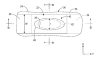
- FIG. 1 is a plan view showing a battery wiring module according to the first embodiment of the present disclosure.
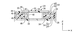
- FIG. 2 is an enlarged plan view of the front and back conductive portions shown in FIG.
- FIG. 3 is an enlarged cross-sectional view of III-III in FIG. 2 ((a) after forming a through hole, (b) after forming a wiring, and (c) a completed view).
- FIG. 4 is an enlarged cross-sectional view of IV-IV in FIG.
- FIG. 5 is an enlarged plan view showing front and back conductive portions of the battery wiring module according to the second embodiment.
- FIG. 6 is an enlarged plan view showing front and back conductive portions of the battery wiring module according to the third embodiment.
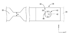
- FIG. 7 is an enlarged plan view showing front and back conductive portions of the battery wiring module according to the fourth embodiment.
- the battery wiring module of the present disclosure is (1) A battery wiring module arranged in a plurality of power storage elements having electrode terminals, the plurality of connecting members connected to the electrode terminals, and the plurality of power storage elements via the plurality of connecting members.
- a flexible printed board having a plurality of voltage detection lines for detecting a voltage is provided, and at least one of the plurality of voltage detection lines includes a front surface wiring formed on the front surface of the flexible printed board and a back surface wiring formed on the back surface.
- It is configured to include front and back conductive portions that penetrate the flexible printed substrate in the plate thickness direction and connect the front and back wirings, and the resistance value per unit length of the front and back conductive portions is the front surface. It is a battery wiring module having a maximum resistance value or less per unit length in the wiring and the back surface wiring.
- At least one of the plurality of voltage detection lines connects the front surface wiring formed on the front surface and the back surface wiring formed on the front surface of the flexible printed substrate, the back surface wiring formed on the back surface, and the front and back surfaces for connecting the front surface wiring and the back surface wiring. It is configured to include a conductive portion. Thereby, for example, when it is desired to change the arrangement order of the voltage detection lines on the connector side connected to the external device in the order of potential, the front side wiring and the back side wiring can be appropriately combined and connected at the front and back conduction portions. Arrays can be realized.
- the resistance value per unit length of the front and back conductive parts is set to be equal to or less than the maximum resistance value per unit length of the front and back wiring, and the voltage detection line in the front and back conductive parts is unexpectedly cut off. The occurrence of defects and short circuits is prevented. As a result, the degree of freedom in arranging the voltage detection line configured by the printed wiring of the flexible printed circuit board can be improved without causing the problem of short circuit.
- the maximum resistance value per unit length in the front side wiring and the back side wiring refers to those in the wiring components, and does not include the current limiting region such as the chip fuse and the positive temperature coefficient thermistor provided in the middle of the wiring.
- the front and back conductive portions have an elliptical shape in which the length direction of the front surface wiring and the back surface wiring is a major axis.
- the front and back conductive parts By forming the front and back conductive parts into an elliptical shape whose long axis is the length direction of the front and back wiring, a large cross-sectional area of the front and back conductive parts is secured for the front and back wirings having a limited wiring width. can do.
- the resistance value per unit length of the front and back conductive portions can be advantageously reduced, and the maximum resistance value per unit length in the front surface wiring and the back surface wiring can be easily realized.
- the front and back conductive parts are filled with through holes that penetrate the multi-layer wiring area where the front and back wirings overlap each other in the plate thickness direction, and the through holes are filled into the front and back wirings, respectively. It may be composed of solder to be connected.
- the front and back conductive portions are composed of a plurality of the vias arranged adjacent to each other.
- the front and back conductive parts By forming the front and back conductive parts with a plurality of vias arranged adjacent to each other, the front and back conductive parts whose resistance value per unit length is equal to or less than the maximum resistance value per unit length in the front surface wiring and the back surface wiring can be formed. This is because it can be realized without increasing the plating thickness. Therefore, it is possible to provide the front and back conductive portions having a lower conduction resistance at a lower cost.
- the hole diameter of the through hole constituting the via is larger than the minimum wiring width dimension in the front surface wiring and the back surface wiring.
- the front surface wiring and the back surface wiring include a metal base layer provided on the flexible printed circuit board and a surface layer provided on the base layer.
- the surface layer is formed by plating at the same time as the metal plating layer provided by adhering to the peripheral wall of the through hole constituting the via, and the thickness dimension of the surface layer is the said. It is preferably made larger than the thickness dimension of the base layer.
- the surface layers of the front surface wiring and the back surface wiring can be formed by plating, and the manufacturing efficiency can be improved.
- the thickness dimension of the surface layer of each wiring is larger than the thickness dimension of the base layer, it is possible to secure a large thickness dimension of the metal plating layer of the via. Therefore, it is possible to advantageously realize that the resistance value per unit length of the front and back conductive portions composed of vias is equal to or less than the maximum resistance value per unit length in the front surface wiring and the back surface wiring.
- the front surface wiring, the back surface wiring, and the front and back conductive portions are covered with an insulating film superposed on them. This is because the front and back conductive portions can be insulated and coated together with the front and back wiring, and the occurrence of a short circuit due to dew condensation or the like on the front and back conductive portions can be prevented.
- the power storage module 10 is mounted on a vehicle (not shown) such as an electric vehicle or a hybrid vehicle, and is arranged on a plurality of (six in this embodiment) power storage elements 12 and a plurality of power storage elements 12. It includes one battery wiring module 14.
- the Z direction will be described as upward, the Y direction as forward in the length direction, and the X direction as right in the width direction.
- a reference numeral may be added to only a part of the members, and the reference numeral may be omitted for the other members.
- the power storage element 12 has a horizontally long rectangular parallelepiped shape, and the power storage module 10 connects six power storage elements 12 in series to increase the output voltage.
- the power storage element 12 is not particularly limited, and may be a secondary battery or a capacitor.
- the power storage element 12 according to this embodiment is a secondary battery.
- a lithium ion secondary battery, a lithium polymer secondary battery, a nickel hydrogen battery, or the like can be used.
- Electrode terminals 16 are formed on the left and right ends of the upper surface of the power storage element 12, respectively.
- One of the electrode terminals 16 is a positive electrode and the other is a negative electrode.
- a connecting bus bar 18 or an output bus bar 20 constituting a connecting member is electrically connected to the electrode terminal 16.
- the connecting bus bar 18 and the output bus bar 20 are formed by pressing a metal plate material into a predetermined shape.
- a metal having high thermal conductivity and low electrical resistance such as copper, copper alloy, aluminum, and aluminum alloy can be appropriately selected.
- a plating layer (not shown) may be formed on the surfaces of the connecting bus bar 18 and the output bus bar 20. Any metal such as tin, nickel, and solder can be selected as the metal constituting the plating layer.
- connection bus bar 18 connects the adjacent electrode terminals 16 to each other while straddling the adjacent electrode terminals 16.
- the output bus bar 20 is connected to one electrode terminal 16 and outputs electric power to an external device (not shown).
- five connecting bus bars 18 connect adjacent electrode terminals 16 to each other.
- a plurality of power storage elements 12 are connected in series by these connection bus bars 18.
- the connection bus bar 18, the output bus bar 20, and the electrode terminal 16 are electrically and physically connected by a known method such as soldering, welding, or bolting.
- the numbers 0 to 6 assigned to the connecting bus bar 18 and the output bus bar 20 indicate the order of potentials of each of the six power storage elements 12 to which the connecting bus bar 18 and the output bus bar 20 are connected. ..
- the potential of the electrode terminal 16 connected to the output bus bar 20 with 0 is the lowest, increasing from 1 to 5, and the potential of the electrode terminal 16 connected to the output bus bar 20 with 6 is the highest. It's getting higher.
- the conventional problem that it is difficult to arrange the surface wirings 30 described later in the order of potential has been solved.
- the potential numbers of the connection bus bar 18 arranged at the left end of the six power storage elements 12 arranged in the front-rear direction and the electrode terminals 16 connected to the output bus bar 20 are 0, 2, 4, It is 6.
- the potential numbers of the electrode terminals 16 connected to the connection bus bars 18 arranged at the right ends of the six power storage elements 12 are 1, 3, and 5. In this way, the potentials of the electrode terminals 16 are divided into left and right in ascending order and are arranged alternately.
- the connector 22 is provided at the connection end of the battery wiring module 14.
- the connector 22 is connected to an external device (not shown) including a circuit for voltage detection or a microcomputer inside.
- a battery wiring module 14 is mounted on the upper surface of the six power storage elements 12.
- the battery wiring module 14 according to the present embodiment includes a flexible two-layer substrate 24 and a connector 22 connected to the two-layer substrate 24.
- the two-layer substrate 24 is a two-layer flexible printed circuit board in which wiring is formed on the front surface 26 and the back surface 28 of the flexible insulating base film 44 described later by a printed wiring technique, respectively. ..
- the two-layer substrate 24 is formed so as to extend in the front-rear direction.
- a plurality of (7 in this embodiment) surface wirings 30 are formed on the surface 26 of the two-layer substrate 24.
- the two surface wires 30 having one end connected to the position of the connector 22 to which 0 or 6 is attached to form a voltage detection line have the other end connected to the output bus bar 20. That is, the two-layer board 24 has two surface wirings 30 that detect the voltage of the power storage element 12 via the two output bus bars 20.
- the surface wiring 30 and the output bus bar 20 are electrically and physically connected by an arbitrary method such as soldering or welding.
- the surface wiring 30 constituting the five voltage detection lines whose one end is connected to the position of the connector 22 to which 1 to 5 is attached has the other end connected to the front and back conductive portions 32.
- the front and back conductive portions 32 penetrate the two-layer substrate 24 in the plate thickness direction (in the direction perpendicular to the paper surface in FIG. 1) to connect the front surface wiring 30 and the back surface wiring 34 formed on the back surface 28 and forming the voltage detection line. doing.
- Each of the five backside wires 34, one end of which is connected to the front and back conductive portions 32, are connected to a connection bus bar 18 whose other end is numbered from 1 to 5.
- the two-layer board 24 has five front surface wirings 30 and five back surface wirings 34 that detect the voltages of the six power storage elements 12 via the five connection bus bars 18.
- the back surface wiring 34 and the connection bus bar 18 are electrically and physically connected by an arbitrary method such as soldering or welding.
- the front-back conductive portion 32 is a projection of the two-layer substrate 24 in the plate thickness direction (in FIG. 2, the direction perpendicular to the paper surface), and the front surface wiring 30 and the back surface wiring 34 are one end portions in the length direction. It is formed in the multilayer wiring region 36 which overlaps with each other.
- the front and back conductive portions 32 are formed by one via 43 composed of a through hole 38 that penetrates the multilayer wiring region 36 in the plate thickness direction and a metal plating layer 42 that adheres to the peripheral wall 40 of the through hole 38 and is formed in a tubular shape. It is configured.
- the front and back conductive portions 32 in the plate thickness direction are connected to the front surface wiring 30 and the back surface wiring 34, respectively.
- the battery wiring module 14 of the present disclosure can be advantageously manufactured.
- the front-back conductive portion 32 has an elliptical shape whose long axis is the length direction (left-right direction in FIG. 2) of the front surface wiring 30 and the back surface wiring 34.
- the metal plating layer 42 is formed thicker at both ends in the length direction than in the center portion in the length direction.
- the length direction as the long axis, it is possible to secure a large cross-sectional area of the front and back conductive portions 32 with respect to the front side wiring 30 and the back side wiring 34 having a constant wiring width. From the above, the resistance value per unit length of the front and back conductive portions 32 can be advantageously reduced. Therefore, it can be easily realized that the maximum resistance value per unit length of the front surface wiring 30 and the back surface wiring 34 or less can be reduced.
- the boundary line of the metal plating layer 42 is described by a virtual line.
- the double-sided copper-clad laminate 48 is subjected to NC drilling, laser machining, or the like to form a through hole 38 penetrating the double-sided copper-clad laminate 48 (see FIG. 3A). ).
- plating treatment is performed over the entire surface of the double-sided copper-clad laminate 48 in which the through hole 38 is formed (for example, electrolytic copper plating treatment).
- electrolytic copper plating treatment for example, electrolytic copper plating treatment.
- the metal plating layer 42 is formed on the copper foil 46 and on the peripheral wall 40 of the through hole 38, and the copper foil 46 formed on both sides of the insulating base film 44 is electrically connected.
- the conductive films (metal plating layer 42 and copper foil 46) on both sides of the insulating base film 44 are processed into a predetermined pattern by a subtractive method (see FIG. 3B).
- the resist layer is exposed and developed by a photofabrication method to resist.
- the layers are processed into a predetermined pattern.
- the metal plating layer 42 and the copper foil 46 are etched using the patterned resist layer as a mask to form the front surface wiring 30 and the back surface wiring 34, and then the resist layer is peeled off.
- the front surface wiring 30 and the back surface wiring 34 are formed on the front surface 26 and the back surface 28 of the insulating base film 44, respectively, and the two-layer substrate 24 having the front and back conduction portions 32 is formed. It is made.
- the plating process is performed after the through holes 38 are formed, but the copper foil 46 may be patterned without performing the plating process.
- a coverlay 54 having an insulating film 50 made of a polyimide film or the like and an adhesive layer 52 formed on one side of the insulating film 50 is prepared.
- the adhesive layer 52 is made of an adhesive such as acrylic or epoxy.
- coverlays 54 are laminated on both sides of the two-layer substrate 24 using a vacuum laminator or the like.
- the front surface wiring 30, the back surface wiring 34, and the front and back conductive portions 32 are covered with the insulating film 50 superimposed on them.
- the front and back conductive portions 32 can be insulated and coated together with the front surface wiring 30 and the back surface wiring 34, and the occurrence of a short circuit due to dew condensation or the like on the front and back conductive portions 32 can be prevented.
- the battery wiring module 14 shown in FIG. 1 is completed.
- the front surface wiring 30 and the back surface wiring 34 form the copper foil 46 forming the metal base layer provided on both sides of the two-layer substrate 24 and the metal plating forming the surface layer provided on the copper foil 46.
- It is configured to include a layer 42.
- the metal plating layer 42 can be simultaneously formed not only on the peripheral wall 40 of the through hole 38 but also on the surface layers of the front surface wiring 30 and the back surface wiring 34, and the manufacturing efficiency can be improved.
- the thickness dimension of the metal plating layer 42 is 18 ⁇ m and the thickness dimension of the copper foil 46 is 15 ⁇ m, and the thickness dimension of the metal plating layer 42 is larger than the thickness dimension of the copper foil 46. It has been enlarged.
- the front and back conductive portions 32 have an elliptical shape whose major axis is the length direction, the metal plating layers 42 are thickly formed at both ends in the length direction, and the peripheral wall 40 constituting the front and back conductive portions 32 is formed. Is elongated in the length direction. Therefore, the resistance value per unit length of the front and back conductive portions 32 is reduced, and it is advantageously realized that the resistance value is equal to or less than the maximum resistance value per unit length of the front surface wiring 30 and the back surface wiring 34.
- the maximum resistance value referred to here refers to those in the wiring components, and does not include a current limiting region such as a chip fuse or a positive temperature coefficient thermistor provided in the middle of the wiring.
- the battery wiring module 14 of the present disclosure having such a structure, it has a front and back conductive portion 32 that penetrates the two-layer substrate 24 in the plate thickness direction and connects the front surface wiring 30 and the back surface wiring 34.
- the resistance value per unit length of the front and back conductive portions 32 is equal to or less than the maximum resistance value per unit length of the front surface wiring 30 and the back surface wiring 34.
- the degree of freedom in allocating the voltage detection line composed of the front side wiring 30 and the back side wiring 34, which are the printed wirings of the two-layer board 24 constituting the flexible printed circuit board, has a problem of short circuit when a jumper wire is used. It can be improved without accompanying.
- the front and back conductive portions 32 are composed of one via 43, but the present invention is not limited to this.
- it may be composed of two vias 43 arranged adjacent to each other in the length direction, such as the front and back conductive portions 56 of the second embodiment shown in FIG.
- it may be composed of four vias 43 arranged adjacent to each other in the length direction and the width direction.
- the front and back conductive portions 56 and 58 in which the resistance value per unit length is equal to or less than the maximum resistance value per unit length in the front surface wiring 30 and the back surface wiring 34 can be realized without increasing the plating thickness of the via 43. Can be done. Therefore, it is possible to provide the front and back conductive portions 56, 58 having a lower conduction resistance at a lower cost.
- the hole diameter in the width direction of the through hole 38 constituting the via 43: r is different in the front surface wiring 30 and the back surface wiring 34.
- Minimum wiring width dimension It was made smaller than W, but is not limited to this.
- the hole diameter: R in the width direction of the through hole 38 constituting the via 43 is the minimum wiring width dimension in the front surface wiring 30 and the back surface wiring 34: w. May be larger than.
- the cross-sectional area of the metal plating layer 42 of the via 43 can be gained more advantageously than the portion of the front surface wiring 30 and the back surface wiring 34 having the minimum wiring width dimension. Therefore, it is possible to advantageously realize that the resistance value per unit length of the front and back conductive portions 60 is equal to or less than the maximum resistance value per unit length of the front surface wiring 30 and the back surface wiring 34.
- the description of the two-layer substrate 24 is omitted in FIG. 7.
- the front and back conductive portions 32, 56, 58, and 60 have the front surface wiring 30 and the back surface wiring 34 formed by the metal plating layer 42 attached to the peripheral wall 40 of the through hole 38. It was a conductive connection, but it is not limited to this.
- the front surface wiring 30 and the back surface wiring 34 may be electrically connected by filling the through holes 38 with solder.
- the description has been made by taking one battery wiring module 14 arranged in the plurality of power storage elements 12 as an example, but the description is not limited to this. It can also be applied to two battery wiring modules 14 arranged on one side and the other side of the plurality of power storage elements 12. In this case, there is no problem that it is difficult to arrange the front surface wiring 30 in the order of potential.
- the resistance adjusting portion connected to the voltage detection line is described in Patent Document 1 by forming the back surface wiring 34. The difference in electrical resistance between the wiring lengths of each voltage detection line can be easily eliminated. As a result, the degree of freedom in arranging the voltage detection line configured by the printed wiring of the flexible printed circuit board can be improved.
- Power storage module 12
- Power storage element 14
- Battery wiring module 16
- Electrode terminal 18
- Connection bus bar (connection member) 20
- Output bus bar (connecting member) 22
- Connector 24
- 2-layer board (flexible printed circuit board) 26
- Front side 28
- Back side 30
- Front side wiring (voltage detection line) 32
- Front and back conduction part 34
- Back side wiring (voltage detection line) 36
- Multi-layer wiring area 38 Through hole 40
- Peripheral wall 42
- Metal plating layer 43 Via 44
- Insulation base film 45
- Adhesive layer 46
- Copper foil 48
- Double-sided copper-clad laminate 50
- Adhesive layer 54
- Coverlay 56
- Front and back conduction part 58
- Front and back conduction Part 60
- Front and back conductive parts 60
Landscapes
- Chemical & Material Sciences (AREA)
- Chemical Kinetics & Catalysis (AREA)
- Electrochemistry (AREA)
- General Chemical & Material Sciences (AREA)
- Engineering & Computer Science (AREA)
- Microelectronics & Electronic Packaging (AREA)
- Power Engineering (AREA)
- Manufacturing & Machinery (AREA)
- Physics & Mathematics (AREA)
- General Physics & Mathematics (AREA)
- Inorganic Chemistry (AREA)
- Battery Mounting, Suspending (AREA)
- Connection Of Batteries Or Terminals (AREA)
- Printing Elements For Providing Electric Connections Between Printed Circuits (AREA)
- Structure Of Printed Boards (AREA)
- Electric Double-Layer Capacitors Or The Like (AREA)
- Fixed Capacitors And Capacitor Manufacturing Machines (AREA)
Priority Applications (2)
| Application Number | Priority Date | Filing Date | Title |
|---|---|---|---|
| US17/773,946 US12219694B2 (en) | 2019-11-13 | 2020-09-30 | Battery wiring module |
| CN202080077857.7A CN114651369B (zh) | 2019-11-13 | 2020-09-30 | 电池布线模块 |
Applications Claiming Priority (2)
| Application Number | Priority Date | Filing Date | Title |
|---|---|---|---|
| JP2019-205196 | 2019-11-13 | ||
| JP2019205196A JP7360089B2 (ja) | 2019-11-13 | 2019-11-13 | 電池配線モジュール |
Publications (1)
| Publication Number | Publication Date |
|---|---|
| WO2021095388A1 true WO2021095388A1 (ja) | 2021-05-20 |
Family
ID=75900032
Family Applications (1)
| Application Number | Title | Priority Date | Filing Date |
|---|---|---|---|
| PCT/JP2020/037166 Ceased WO2021095388A1 (ja) | 2019-11-13 | 2020-09-30 | 電池配線モジュール |
Country Status (4)
| Country | Link |
|---|---|
| US (1) | US12219694B2 (https=) |
| JP (1) | JP7360089B2 (https=) |
| CN (1) | CN114651369B (https=) |
| WO (1) | WO2021095388A1 (https=) |
Cited By (1)
| Publication number | Priority date | Publication date | Assignee | Title |
|---|---|---|---|---|
| WO2024122238A1 (ja) * | 2022-12-05 | 2024-06-13 | 矢崎総業株式会社 | 積層回路体、及び、バスバモジュール |
Families Citing this family (4)
| Publication number | Priority date | Publication date | Assignee | Title |
|---|---|---|---|---|
| US12506227B2 (en) * | 2020-07-14 | 2025-12-23 | Autonetworks Technologies, Ltd. | Wiring module |
| CN114824859B (zh) * | 2022-01-05 | 2025-06-27 | 浙江新富尔电子有限公司 | 一种接电组件和新能源汽车电池检测模组 |
| KR20240088377A (ko) * | 2022-12-13 | 2024-06-20 | 삼성에스디아이 주식회사 | 이차 전지 모듈 |
| WO2024247904A1 (ja) | 2023-05-31 | 2024-12-05 | 株式会社村田製作所 | 伸縮性デバイス |
Citations (4)
| Publication number | Priority date | Publication date | Assignee | Title |
|---|---|---|---|---|
| JPH09181453A (ja) * | 1995-12-21 | 1997-07-11 | Sony Corp | 多層配線基板及びその製造方法 |
| JP2001068856A (ja) * | 1999-06-22 | 2001-03-16 | Asahi Chem Ind Co Ltd | 絶縁樹脂シート及びその製造方法 |
| JP2017045845A (ja) * | 2015-08-26 | 2017-03-02 | イビデン株式会社 | 回路基板及び回路基板の製造方法 |
| JP2019114464A (ja) * | 2017-12-25 | 2019-07-11 | 株式会社デンソー | 監視装置 |
Family Cites Families (13)
| Publication number | Priority date | Publication date | Assignee | Title |
|---|---|---|---|---|
| JPH06216488A (ja) * | 1993-01-19 | 1994-08-05 | Canon Inc | プリント配線板及びその加工方法 |
| JP2000151111A (ja) * | 1998-08-31 | 2000-05-30 | Toppan Printing Co Ltd | 半導体装置用基板 |
| JP2007250616A (ja) | 2006-03-14 | 2007-09-27 | Epson Imaging Devices Corp | フレキシブル回路基板、フレキシブル回路基板の製造方法、及び電気光学装置、並びに電子機器 |
| EP2506338B1 (en) * | 2007-11-29 | 2013-11-13 | LG Chem, Ltd. | Battery pack containing PCM employed with safety member |
| JP5710152B2 (ja) * | 2010-04-15 | 2015-04-30 | 日本メクトロン株式会社 | 多層フレキシブルプリント配線板の製造方法 |
| JP5518624B2 (ja) * | 2010-08-10 | 2014-06-11 | 日本メクトロン株式会社 | プリント配線板及びその製造方法 |
| JP2013062451A (ja) | 2011-09-15 | 2013-04-04 | Hitachi Cable Ltd | フレキシブル配線基板およびフレキシブル配線基板の製造方法 |
| JPWO2014024452A1 (ja) | 2012-08-09 | 2016-07-25 | 三洋電機株式会社 | バッテリシステム及びこのバッテリシステムを備える電動車両並びに蓄電装置 |
| JP2014075457A (ja) | 2012-10-03 | 2014-04-24 | Sumitomo Electric Printed Circuit Inc | プリント配線板及びその製造方法 |
| JP6257889B2 (ja) * | 2012-10-23 | 2018-01-10 | 日本メクトロン株式会社 | バスバー付きフレキシブルプリント配線板およびその製造方法、並びにバッテリシステム |
| JP2016127248A (ja) * | 2015-01-08 | 2016-07-11 | 日本特殊陶業株式会社 | 多層配線基板 |
| JP6874544B2 (ja) * | 2017-06-07 | 2021-05-19 | 株式会社デンソー | 監視装置 |
| CN110247056A (zh) * | 2018-03-30 | 2019-09-17 | 宁德时代新能源科技股份有限公司 | 一种集流体,其极片和电化学装置 |
-
2019
- 2019-11-13 JP JP2019205196A patent/JP7360089B2/ja active Active
-
2020
- 2020-09-30 CN CN202080077857.7A patent/CN114651369B/zh active Active
- 2020-09-30 US US17/773,946 patent/US12219694B2/en active Active
- 2020-09-30 WO PCT/JP2020/037166 patent/WO2021095388A1/ja not_active Ceased
Patent Citations (4)
| Publication number | Priority date | Publication date | Assignee | Title |
|---|---|---|---|---|
| JPH09181453A (ja) * | 1995-12-21 | 1997-07-11 | Sony Corp | 多層配線基板及びその製造方法 |
| JP2001068856A (ja) * | 1999-06-22 | 2001-03-16 | Asahi Chem Ind Co Ltd | 絶縁樹脂シート及びその製造方法 |
| JP2017045845A (ja) * | 2015-08-26 | 2017-03-02 | イビデン株式会社 | 回路基板及び回路基板の製造方法 |
| JP2019114464A (ja) * | 2017-12-25 | 2019-07-11 | 株式会社デンソー | 監視装置 |
Cited By (3)
| Publication number | Priority date | Publication date | Assignee | Title |
|---|---|---|---|---|
| WO2024122238A1 (ja) * | 2022-12-05 | 2024-06-13 | 矢崎総業株式会社 | 積層回路体、及び、バスバモジュール |
| JP2024080960A (ja) * | 2022-12-05 | 2024-06-17 | 矢崎総業株式会社 | 積層回路体、及び、バスバモジュール |
| JP7712251B2 (ja) | 2022-12-05 | 2025-07-23 | 矢崎総業株式会社 | 積層回路体、及び、バスバモジュール |
Also Published As
| Publication number | Publication date |
|---|---|
| CN114651369B (zh) | 2024-10-08 |
| US12219694B2 (en) | 2025-02-04 |
| JP2021077579A (ja) | 2021-05-20 |
| JP7360089B2 (ja) | 2023-10-12 |
| US20220377881A1 (en) | 2022-11-24 |
| CN114651369A (zh) | 2022-06-21 |
Similar Documents
| Publication | Publication Date | Title |
|---|---|---|
| JP7360089B2 (ja) | 電池配線モジュール | |
| JP6257889B2 (ja) | バスバー付きフレキシブルプリント配線板およびその製造方法、並びにバッテリシステム | |
| CN108511666B (zh) | 导电模块和电池组 | |
| US9089082B2 (en) | Printed circuit board with embedded component and method for manufacturing same | |
| JP2024512188A (ja) | 多層フレキシブルバッテリー相互接続及びその製造方法 | |
| US9024203B2 (en) | Embedded printed circuit board and method for manufacturing same | |
| JP2021077579A5 (https=) | ||
| CN107078263A (zh) | 用于蓄电池组的互连件 | |
| US9019709B2 (en) | Protective circuit module | |
| WO2009141928A1 (ja) | プリント配線板及びその製造方法 | |
| JP2015035497A (ja) | 電子部品内蔵配線板 | |
| KR20220064614A (ko) | 인쇄회로기판 및 이를 구비하는 배터리 장치 | |
| JP2008294351A (ja) | 配線回路基板 | |
| JP7315546B2 (ja) | 部品内蔵基板 | |
| JP6258437B2 (ja) | バスバー付きフレキシブルプリント配線板の製造方法 | |
| EP0287681A1 (en) | Multi-layer printed circuit board and a method of fabricating the same | |
| WO2023037889A1 (ja) | 配線モジュール | |
| JP4152905B2 (ja) | コンデンサモジュール装置 | |
| US12362437B2 (en) | Multilayered flexible interconnect circuits for battery assemblies and methods of fabricating and installing thereof | |
| JP4799349B2 (ja) | 電源分配装置およびその製造方法 | |
| CN121220189A (zh) | 包括围绕凸台孔的电流线的pcb | |
| RU2600037C2 (ru) | Тканая монтажная плата и способ ее изготовления | |
| JP2017212431A (ja) | キャパシタ及びこれを含む回路基板 | |
| JPH10302605A (ja) | チップフューズおよびその製造法 | |
| JP2020178113A (ja) | フレキシブル配線板 |
Legal Events
| Date | Code | Title | Description |
|---|---|---|---|
| 121 | Ep: the epo has been informed by wipo that ep was designated in this application |
Ref document number: 20886634 Country of ref document: EP Kind code of ref document: A1 |
|
| NENP | Non-entry into the national phase |
Ref country code: DE |
|
| 122 | Ep: pct application non-entry in european phase |
Ref document number: 20886634 Country of ref document: EP Kind code of ref document: A1 |