WO2021090861A1 - 弾性波装置 - Google Patents
弾性波装置 Download PDFInfo
- Publication number
- WO2021090861A1 WO2021090861A1 PCT/JP2020/041292 JP2020041292W WO2021090861A1 WO 2021090861 A1 WO2021090861 A1 WO 2021090861A1 JP 2020041292 W JP2020041292 W JP 2020041292W WO 2021090861 A1 WO2021090861 A1 WO 2021090861A1
- Authority
- WO
- WIPO (PCT)
- Prior art keywords
- silicon carbide
- elastic wave
- wave device
- carbide substrate
- layer
- Prior art date
- Legal status (The legal status is an assumption and is not a legal conclusion. Google has not performed a legal analysis and makes no representation as to the accuracy of the status listed.)
- Ceased
Links
Images








Classifications
-
- H—ELECTRICITY
- H03—ELECTRONIC CIRCUITRY
- H03H—IMPEDANCE NETWORKS, e.g. RESONANT CIRCUITS; RESONATORS
- H03H9/00—Networks comprising electromechanical or electro-acoustic elements; Electromechanical resonators
- H03H9/02—Details
- H03H9/02535—Details of surface acoustic wave devices
- H03H9/02543—Characteristics of substrate, e.g. cutting angles
- H03H9/02574—Characteristics of substrate, e.g. cutting angles of combined substrates, multilayered substrates, piezoelectrical layers on not-piezoelectrical substrate
-
- H—ELECTRICITY
- H03—ELECTRONIC CIRCUITRY
- H03H—IMPEDANCE NETWORKS, e.g. RESONANT CIRCUITS; RESONATORS
- H03H9/00—Networks comprising electromechanical or electro-acoustic elements; Electromechanical resonators
- H03H9/02—Details
- H03H9/02007—Details of bulk acoustic wave devices
- H03H9/02047—Treatment of substrates
-
- H—ELECTRICITY
- H03—ELECTRONIC CIRCUITRY
- H03H—IMPEDANCE NETWORKS, e.g. RESONANT CIRCUITS; RESONATORS
- H03H9/00—Networks comprising electromechanical or electro-acoustic elements; Electromechanical resonators
- H03H9/02—Details
- H03H9/02007—Details of bulk acoustic wave devices
- H03H9/02015—Characteristics of piezoelectric layers, e.g. cutting angles
-
- H—ELECTRICITY
- H03—ELECTRONIC CIRCUITRY
- H03H—IMPEDANCE NETWORKS, e.g. RESONANT CIRCUITS; RESONATORS
- H03H9/00—Networks comprising electromechanical or electro-acoustic elements; Electromechanical resonators
- H03H9/02—Details
- H03H9/02007—Details of bulk acoustic wave devices
- H03H9/02086—Means for compensation or elimination of undesirable effects
-
- H—ELECTRICITY
- H03—ELECTRONIC CIRCUITRY
- H03H—IMPEDANCE NETWORKS, e.g. RESONANT CIRCUITS; RESONATORS
- H03H9/00—Networks comprising electromechanical or electro-acoustic elements; Electromechanical resonators
- H03H9/02—Details
- H03H9/02535—Details of surface acoustic wave devices
- H03H9/02543—Characteristics of substrate, e.g. cutting angles
- H03H9/02559—Characteristics of substrate, e.g. cutting angles of lithium niobate or lithium-tantalate substrates
-
- H—ELECTRICITY
- H03—ELECTRONIC CIRCUITRY
- H03H—IMPEDANCE NETWORKS, e.g. RESONANT CIRCUITS; RESONATORS
- H03H9/00—Networks comprising electromechanical or electro-acoustic elements; Electromechanical resonators
- H03H9/02—Details
- H03H9/02535—Details of surface acoustic wave devices
- H03H9/02818—Means for compensation or elimination of undesirable effects
-
- H—ELECTRICITY
- H03—ELECTRONIC CIRCUITRY
- H03H—IMPEDANCE NETWORKS, e.g. RESONANT CIRCUITS; RESONATORS
- H03H9/00—Networks comprising electromechanical or electro-acoustic elements; Electromechanical resonators
- H03H9/02—Details
- H03H9/02535—Details of surface acoustic wave devices
- H03H9/02818—Means for compensation or elimination of undesirable effects
- H03H9/02866—Means for compensation or elimination of undesirable effects of bulk wave excitation and reflections
-
- H—ELECTRICITY
- H03—ELECTRONIC CIRCUITRY
- H03H—IMPEDANCE NETWORKS, e.g. RESONANT CIRCUITS; RESONATORS
- H03H9/00—Networks comprising electromechanical or electro-acoustic elements; Electromechanical resonators
- H03H9/02—Details
- H03H9/05—Holders or supports
- H03H9/0504—Holders or supports for bulk acoustic wave devices
-
- H—ELECTRICITY
- H03—ELECTRONIC CIRCUITRY
- H03H—IMPEDANCE NETWORKS, e.g. RESONANT CIRCUITS; RESONATORS
- H03H9/00—Networks comprising electromechanical or electro-acoustic elements; Electromechanical resonators
- H03H9/02—Details
- H03H9/05—Holders or supports
- H03H9/058—Holders or supports for surface acoustic wave devices
-
- H—ELECTRICITY
- H03—ELECTRONIC CIRCUITRY
- H03H—IMPEDANCE NETWORKS, e.g. RESONANT CIRCUITS; RESONATORS
- H03H9/00—Networks comprising electromechanical or electro-acoustic elements; Electromechanical resonators
- H03H9/02—Details
- H03H9/05—Holders or supports
- H03H9/0595—Holders or supports the holder support and resonator being formed in one body
-
- H—ELECTRICITY
- H03—ELECTRONIC CIRCUITRY
- H03H—IMPEDANCE NETWORKS, e.g. RESONANT CIRCUITS; RESONATORS
- H03H9/00—Networks comprising electromechanical or electro-acoustic elements; Electromechanical resonators
- H03H9/02—Details
- H03H9/125—Driving means, e.g. electrodes, coils
- H03H9/145—Driving means, e.g. electrodes, coils for networks using surface acoustic waves
- H03H9/14538—Formation
- H03H9/14541—Multilayer finger or busbar electrode
-
- H—ELECTRICITY
- H03—ELECTRONIC CIRCUITRY
- H03H—IMPEDANCE NETWORKS, e.g. RESONANT CIRCUITS; RESONATORS
- H03H9/00—Networks comprising electromechanical or electro-acoustic elements; Electromechanical resonators
- H03H9/15—Constructional features of resonators consisting of piezoelectric or electrostrictive material
- H03H9/17—Constructional features of resonators consisting of piezoelectric or electrostrictive material having a single resonator
- H03H9/171—Constructional features of resonators consisting of piezoelectric or electrostrictive material having a single resonator implemented with thin-film techniques, i.e. of the film bulk acoustic resonator [FBAR] type
-
- H—ELECTRICITY
- H03—ELECTRONIC CIRCUITRY
- H03H—IMPEDANCE NETWORKS, e.g. RESONANT CIRCUITS; RESONATORS
- H03H9/00—Networks comprising electromechanical or electro-acoustic elements; Electromechanical resonators
- H03H9/25—Constructional features of resonators using surface acoustic waves
Definitions
- the present invention relates to an elastic wave device.
- Patent Document 1 discloses an example of an elastic wave device.
- a piezoelectric film is provided on a support substrate, and an IDT (Interdigital Transducer) electrode is provided on the piezoelectric film.
- Silicon, silicon carbide, or the like is used for the support substrate.
- Lithium tantalate, lithium niobate, and the like are used for the piezoelectric film.
- An object of the present invention is to provide an elastic wave device that uses a silicon carbide substrate as a support substrate and can suppress a higher-order mode.
- the elastic wave device includes a support substrate, a piezoelectric layer provided on the support substrate, and an IDT electrode provided on the piezoelectric layer and having a plurality of electrode fingers, and includes a support substrate.
- the piezoelectric layer is a lithium tantalate layer or a lithium niobate layer
- SH waves are used as the main mode.
- an elastic wave device that uses a silicon carbide substrate as a support substrate and can suppress a higher-order mode.
- FIG. 1 is a front sectional view of an elastic wave device according to a first embodiment of the present invention.
- FIG. 2 is a plan view of the elastic wave device according to the first embodiment of the present invention.
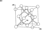
- FIG. 3 is a schematic diagram showing the definition of the crystal axis of silicon carbide.
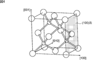
- FIG. 4 is a schematic view showing the (100) plane of silicon carbide.
- FIG. 5 is a schematic view showing the (110) plane of silicon carbide.
- FIG. 6 is a diagram showing the intensity of higher-order modes in the first embodiment of the present invention and the first comparative example.
- FIG. 7 is a diagram showing the relationship between the cut angle of the lithium tantalate layer and the electromechanical coupling coefficient for SH waves and SV waves.
- FIG. 1 is a front sectional view of an elastic wave device according to a first embodiment of the present invention.
- FIG. 2 is a plan view of the elastic wave device according to the first embodiment of the present invention.
- FIG. 3 is a schematic diagram showing the definition of the
- FIG. 8 is a diagram showing the relationship between the thickness of the IDT electrode and the Q value.
- FIG. 9 is a diagram showing the relationship between the angle formed by the S direction, which is the propagation direction of surface acoustic waves, and the [001] direction in the crystal structure of the silicon carbide substrate, and the characteristics of the main mode.
- FIG. 10 is a schematic diagram for explaining the angle ⁇ .
- FIG. 11 is a diagram showing the relationship between ⁇ LT , angle ⁇ , and the electromechanical coupling coefficient ksaw 2 of spurious due to Rayleigh waves at Euler angles of the lithium tantalate layer.
- FIG. 13 is a front sectional view of an elastic wave device according to a modified example of the first embodiment of the present invention.
- FIG. 14 is a diagram showing the relationship between the thickness of the bass velocity film and the specific band.
- FIG. 15 is a diagram showing the relationship between the thickness of the bass velocity film and the phase of the higher-order mode that occurs at a frequency near 1.5 times the frequency of the main mode.
- FIG. 16 is a diagram showing the relationship between the thickness of the bass velocity film and the phase of the higher-order mode that occurs at a frequency near twice the frequency of the main mode.
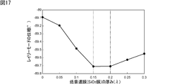
- FIG. 17 is a diagram showing the relationship between the thickness of the bass velocity film and the phase of the Rayleigh mode.
- FIG. 18 is a front sectional view of the elastic wave device according to the second embodiment of the present invention.
- FIG. 18 is a front sectional view of the elastic wave device according to the second embodiment of the present invention.
- FIG. 19 is a diagram showing the intensity of the higher-order mode generated in the vicinity of 1.5 times the frequency of the main mode in the second embodiment and the second comparative example of the present invention.
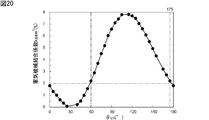
- FIG. 20 is a diagram showing the relationship between ⁇ LN at Euler angles of the lithium niobate layer and the electromechanical coupling coefficient of SH waves.
- FIG. 21 is a diagram showing the relationship between ⁇ LN at the Euler angles of the lithium niobate layer and the phase of spurious in the higher-order mode generated at a frequency near three times the frequency of the main mode.
- FIG. 22 is a diagram showing the relationship between ⁇ LN at Euler angles of the lithium niobate layer and the phase of spurious caused by Rayleigh waves.
- FIG. 20 is a diagram showing the relationship between ⁇ LN at Euler angles of the lithium niobate layer and the electromechanical coupling coefficient of SH waves.
- FIG. 21 is a diagram showing the relationship between ⁇ LN at the Euler angles of the
- FIG. 23 is a diagram showing the relationship between the angle formed by the S direction, which is the propagation direction of surface acoustic waves, and the [001] direction in the crystal structure of the silicon carbide substrate, and the characteristics of the main mode.
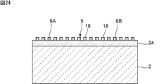
- FIG. 24 is a front sectional view of an elastic wave device according to a modified example of the second embodiment of the present invention.
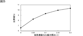
- FIG. 25 is a diagram showing the relationship between the thickness of the bass velocity film and the specific band.
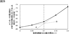
- FIG. 26 is a diagram showing the relationship between the thickness of the bass velocity film and the phase of the higher-order mode that occurs at a frequency near twice the frequency of the main mode.
- FIG. 1 is a front sectional view of an elastic wave device according to a first embodiment of the present invention.
- the elastic wave device 1 has a support substrate.
- the support substrate of this embodiment is a silicon carbide substrate 2. More specifically, the crystal structure of the silicon carbide substrate 2 is a 3C-SiC type cubic crystal structure.
- a bass velocity film 3 is provided on the silicon carbide substrate 2.
- a piezoelectric layer is provided on the bass velocity film 3.
- the piezoelectric layer of this embodiment is the lithium tantalate layer 4.
- the piezoelectric layer may be a lithium niobate layer.
- An IDT electrode 5 is provided on the lithium tantalate layer 4. By applying an AC voltage to the IDT electrode 5, elastic waves in various modes are excited.
- the elastic wave device 1 uses SH waves as the main mode.
- the sound velocity of the slow transverse wave of the bulk wave propagating in the silicon carbide substrate 2 is higher than the sound velocity of the SH wave propagating in the piezoelectric layer. More specifically, the sound velocity of the slow transverse wave of the bulk wave propagating in the silicon carbide substrate 2 is higher than the sound velocity of the SH wave propagating in the piezoelectric layer at the antiresonance frequency.
- the speed of sound of the slow transverse wave propagating in the silicon carbide substrate 2 is V Low
- the sound velocity of the SH wave propagating in the piezoelectric layer is V SH
- the antiresonance frequency of the SH wave propagating in the piezoelectric layer is set.
- V Sha V Low > V Sha
- the relationship does not necessarily have to be V Low > V Sha. At frequencies other than the antiresonance frequency, the relationship of V Low > V SH may be established.
- the elastic wave device 1 of the present embodiment is an elastic wave resonator.
- the elastic wave device 1 according to the present invention is not limited to the elastic wave resonators, and may be a filter device or the like having a plurality of elastic wave resonators.
- FIG. 2 is a plan view of the elastic wave device according to the first embodiment.
- the IDT electrode 5 has a first bus bar 16 and a second bus bar 17 facing each other.
- the IDT electrode 5 has a plurality of first electrode fingers 18 each having one end connected to the first bus bar 16. Further, the IDT electrode 5 has a plurality of second electrode fingers 19 each having one end connected to the second bus bar 17.
- the plurality of first electrode fingers 18 and the plurality of second electrode fingers 19 are interleaved with each other.
- the propagation direction of the surface acoustic wave is defined as the S direction
- the direction orthogonal to the S direction is defined as the L direction.
- the L direction is the direction in which the first electrode finger 18 and the second electrode finger 19 extend.
- the IDT electrode 5 is made of a single layer Al film.
- the materials of the reflector 6A and the reflector 6B are the same as those of the IDT electrode 5.
- the materials of the IDT electrode 5, the reflector 6A and the reflector 6B are not limited to the above.
- the IDT electrode 5, the reflector 6A and the reflector 6B may be made of a laminated metal film in which a plurality of metal layers are laminated.
- the bass velocity film 3 shown in FIG. 1 is a film having a relatively low sound velocity. More specifically, the sound velocity of the bulk wave propagating in the bass velocity film 3 is lower than the sound velocity of the bulk wave propagating in the lithium tantalate layer 4 as the piezoelectric layer.
- the bass velocity film 3 of the present embodiment is a silicon oxide film. Silicon oxide is represented by SiO x. x is any positive number. The silicon oxide constituting the bass velocity film 3 of the present embodiment is SiO 2 .
- the material of the bass velocity film 3 is not limited to the above, and for example, a material containing glass, silicon nitride, lithium oxide, or a compound obtained by adding fluorine, carbon, or boron to silicon oxide may be used. it can.
- the lithium tantalate layer 4 is indirectly laminated on the silicon carbide substrate 2 via the low sound velocity film 3.
- the lithium tantalate layer 4 may be directly laminated on the silicon carbide substrate 2.
- FIG. 3 is a schematic diagram showing the definition of the crystal axis of silicon carbide.
- FIG. 4 is a schematic view showing the (100) plane of silicon carbide.
- FIG. 5 is a schematic view showing the (110) plane of silicon carbide.
- the silicon carbide substrate 2 is a 3C-SiC type cubic silicon carbide single crystal substrate.
- the crystal axis of the silicon carbide constituting the silicon carbide substrate 2 is (X, Y, Z).
- the X-axis, Y-axis, and Z-axis are equivalent due to the symmetry of the crystal structure.
- the plane orientation of the silicon carbide substrate 2 in the elastic wave device 1 is, for example, (100).
- (100) indicates that the substrate is cut in the (100) plane orthogonal to the crystal axis represented by the Miller index [100] in the crystal structure.
- the (100) plane is the plane shown in FIG. However, it also includes other crystallographically equivalent surfaces.
- the main surface of the silicon carbide substrate 2 is not limited to the (100) surface, and may be, for example, the (110) surface shown in FIG.
- the Euler angles of the silicon carbide substrate 2 be ( ⁇ SiC , ⁇ SiC , ⁇ SiC ).
- each of the above surfaces of the silicon carbide substrate 2 is displayed by Euler angles, it is (90 °, 90 °, ⁇ SiC ) in the case of the (100) surface, and (-45 °,-45 °,-in the case of the (110) surface. 90 °, 90 °).
- the plane orientation or Euler angles of the silicon carbide substrate 2 are not limited to these.
- the X-axis direction is assumed to be the same direction as the [100] direction
- the Y-axis direction is assumed to be the same direction as the [010] direction
- the Z-axis direction is [001]. ] It is assumed that the direction is the same as the direction.
- the feature of this embodiment is that the lithium tantalate layer 4 and the silicon carbide substrate 2 having a 3C-SiC type cubic structure are laminated, and the elastic wave device 1 uses the SH mode. Thereby, in the elastic wave device 1 using the silicon carbide substrate 2, the higher-order mode can be suppressed. The details will be described below.
- ⁇ be the wavelength defined by the electrode finger pitch of the IDT electrode 5.
- the electrode finger pitch is an average value of the distances between the center of the electrode fingers of adjacent electrode fingers in the IDT electrode 5.
- Silicon Carbide Substrate 2 Material: 3C-SiC type cubic SiC, plane orientation: (100), thickness: 1 ⁇ m Bass velocity film 3; Material: SiO 2 , Thickness: 0.1 ⁇ Lithium tantalate layer 4; Material: 35 ° Y-LiTaO 3 , Thickness: 0.15 ⁇ IDT electrode 5; material ... Al, thickness ... 0.05 ⁇
- a first comparative example an elastic wave device in which the silicon carbide used for the silicon carbide substrate has a 4H-SiC type hexagonal structure was prepared.
- the design parameters of the first comparative example are the same as the design parameters of the elastic wave device 1 except for the silicon carbide substrate.
- the intensities of the higher-order modes were compared between the elastic wave device 1 having the configuration of the first embodiment and the first comparative example.
- FIG. 6 is a diagram showing the intensity of the higher-order mode in the first embodiment and the first comparative example.
- the sound velocity of the higher-order mode propagating in the piezoelectric layer is higher than the sound velocity of the slow transverse wave of the bulk wave propagating in the silicon carbide substrate 2.
- the higher-order mode leaks to the silicon carbide substrate 2 side, so that the higher-order mode can be suppressed more reliably.
- the electromechanical coupling coefficient of each mode excited by the elastic wave device 1 depends on the cut angle of lithium tantalate used for the lithium tantalate layer 4.
- the range of the cut angle suitable for using the SH wave as the main mode is shown below.
- FIG. 7 is a diagram showing the relationship between the cut angle of the lithium tantalate layer and the electromechanical coupling coefficient of the SH wave and the SV wave.
- an SV wave is excited in addition to the SH wave.
- the electromechanical coupling coefficient of the SH wave is the electromechanical coupling coefficient of the SV wave. It can be seen that it is larger than the coupling coefficient. Therefore, within the range of the cut angle, the excitation intensity of the SH wave is larger than the excitation intensity of the SV wave in the other mode. Therefore, it is preferable that the cut angle of the lithium tantalate layer is 0 ° or more and 10 ° or less, and 50 ° or more and 180 ° or less.
- the SH wave can be preferably used as the main mode.
- the thickness of the IDT electrode 5 is preferably 0.07 ⁇ or less. Thereby, the Q value can be increased. This will be described below.
- a plurality of elastic wave devices 1 having the configuration of the first embodiment and having the following design parameters and different thicknesses of the IDT electrodes 5 were prepared.
- Silicon Carbide Substrate 2 Silicon Carbide Substrate 2; Material ... 3C-SiC type cubic structure SiC, plane orientation ... (100) Bass velocity film 3; Material: SiO 2 , Thickness: 0.1 ⁇ Lithium tantalate layer 4; Material: 35 ° Y-LiTaO 3 , Thickness: 0.15 ⁇ IDT electrode; material: Al, thickness: 0.01 or more, and 0.15 ⁇ or less.
- FIG. 8 is a diagram showing the relationship between the thickness of the IDT electrode and the Q value.
- the thickness of the IDT electrode 5 is 0.07 ⁇ or less, it can be seen that the Q value is high and the change in the Q value is small. Therefore, as described above, the thickness of the IDT electrode 5 is preferably 0.07 ⁇ or less.
- the characteristics of the main mode are changed. I examined.
- the design parameters are as follows.
- the angles formed by the S direction and the Z axis direction were set to 0 °, 12 °, 16 °, 20 °, 24 ° or 28 °.
- the Z axis and the [001] direction are the same direction because of the symmetry of the crystal structure. Therefore, in the present specification, the angle formed by the S direction and the Z-axis direction may be described as the angle formed by the S direction and the [001] direction.
- Silicon Carbide Substrate 2 Silicon Carbide Substrate 2; Material ... 3C-SiC type cubic structure SiC, plane orientation ... (100) Bass velocity film 3; Material: SiO 2 , Thickness: 0.1 ⁇ Lithium tantalate layer 4; Material: 40 ° Y-LiTaO 3 , Thickness: 0.1 ⁇ IDT electrode 5; material ... Al, thickness ... 0.14 ⁇
- FIG. 9 is a diagram showing the relationship between the angle formed by the S direction, which is the propagation direction of surface acoustic waves, and the [001] direction in the crystal structure of the silicon carbide substrate, and the characteristics of the main mode.
- FIG. 9 shows the case where the angles are 0 °, 12 °, 16 °, 20 °, 24 ° or 28 °, respectively.
- the angle formed by the S direction and the [001] direction is 20 ° or less, it can be seen that the characteristics of the main mode are good. Therefore, when the main surface of the silicon carbide substrate 2 is the (100) surface, the angle formed by the S direction and the [001] direction is preferably 20 ° or less.
- the angle formed by the S direction and the [001] direction is preferably 20 ° or less.
- FIG. 9 shows a case where the angle formed by the S direction and the [001] direction is changed.
- the angle formed by the S direction and the [001] direction is set to 0 °.
- the angle formed by the [100] direction in the crystal structure of the silicon carbide substrate 2 shown in FIG. 3 and the L direction in which the electrode finger of the IDT electrode 5 shown in FIG. 2 extends is defined as ⁇ .
- An example of the angle ⁇ is shown in FIG.
- the Euler angles of the lithium tantalate layer 4 be ( ⁇ LT , ⁇ LT , ⁇ LT ). The relationship between ⁇ LT at Euler angles of lithium tantalate layer 4, angles ⁇ , and spurious emissions by Rayleigh waves was determined.
- FIG. 11 is a diagram showing the relationship between ⁇ LT , angle ⁇ , and the electromechanical coupling coefficient ksaw 2 of spurious due to Rayleigh waves at Euler angles of the lithium tantalate layer.
- the region where ksaw 2 ⁇ 0.10. Is shown by hatching.
- ⁇ LT and angles at Euler angles of lithium tantalate layers where the electromechanical coupling coefficients of spurious due to Rayleigh waves are 0.10, 0.20, 0.30, 0.40 and 0.50, respectively.
- the relationship of ⁇ is shown.
- the conditions under which ksaw 2 ⁇ 0.10 or less are shown by the following equations 1 and 2.
- the electromechanical coupling coefficient ksaw 2 of spurious due to Rayleigh waves can be set to 0.10 or less (within the region shown by hatching in FIG. 11), and spurious can be effectively suppressed. can do.
- the sound velocity V Low of the slow transverse wave propagating in the silicon carbide substrate 2 is higher than the sound velocity V SH of the elastic wave propagating in the piezoelectric layer.
- the thickness of the IDT electrode is T IDT .
- Equation 3 is an equation showing the relationship between ⁇ SiC and TIDT shown in FIG.
- the sound velocity V Low of the slow transverse wave propagating on the silicon carbide substrate 2 can be made higher than the sound velocity V SH of the SH wave propagating on the silicon carbide substrate 2. Thereby, the higher-order mode can be suppressed more reliably.
- FIG. 13 is a front sectional view of the elastic wave device according to the modified example of the first embodiment.
- the lithium tantalate layer 4 is directly provided on the silicon carbide substrate 2.
- the higher-order mode can be suppressed as in the first embodiment.
- the elastic wave device 1 has a bass velocity film 3 provided between the silicon carbide substrate 2 and the lithium tantalate layer 4. Thereby, the specific band can be suitably increased. This effect is shown below.
- the specific band the resonance frequency F r, the antiresonance frequency when the F a, represented by (F a -F r) / F r.
- a plurality of elastic wave devices 1 having the configuration of the first embodiment and having different thicknesses of the bass velocity film 3 were prepared.
- an elastic wave device according to a modification of the first embodiment, which does not have the bass speed film 3 and has a thickness of the bass speed film 3 of 0, is also prepared.
- the specific band was examined in each of the above-mentioned plurality of elastic wave devices.
- the design parameters of the plurality of elastic wave devices are as follows.
- Silicon Carbide Substrate 2 Material: 3C-SiC type cubic SiC Bass sound film 3; Material: SiO 2 , Thickness: 0 or more, 0.3 ⁇ or less, changed in 0.05 ⁇ increments.
- Lithium tantalate layer 4 Material: 35 ° Y-LiTaO 3 , Thickness: 0.15 ⁇ IDT electrode 5; material ... Al, thickness ... 0.05 ⁇ Wavelength ⁇ of IDT electrode 5; 1 ⁇ m
- FIG. 14 is a diagram showing the relationship between the thickness of the bass velocity film and the specific band. Note that FIG. 14 also shows the result when the bass velocity film 3 is not provided.
- the thickness of the bass velocity film 3 is 0, and the specific band is wider when the bass velocity film 3 is provided than when the bass velocity film 3 is not provided. You can see that there is. Further, it can be seen that the thicker the bass velocity film 3, the wider the specific band. As shown in FIG. 14, when the thickness of the bass velocity film 3 is 0.2 ⁇ or more, the variation in the specific band with respect to the variation in the thickness of the bass velocity film 3 can be reduced. Therefore, the thickness of the bass velocity film 3 is preferably 0.2 ⁇ or more.
- a plurality of elastic wave devices having the same design parameters as the plurality of elastic wave devices whose specific bands shown in FIG. 14 were investigated were prepared.
- the phase of the higher-order mode generated at a frequency near 1.5 times the frequency of the main mode and the phase of the higher-order mode generated at a frequency near twice the frequency of the main mode were measured. .. Further, in the above-mentioned plurality of elastic wave devices, the phase of the Rayleigh mode as a spurious was measured.
- FIG. 15 is a diagram showing the relationship between the thickness of the bass velocity film and the phase of the higher-order mode that occurs at a frequency near 1.5 times the frequency of the main mode.
- the thinner the bass velocity film 3 the more the higher-order mode that occurs at a frequency near 1.5 times the frequency of the main mode is suppressed.
- the thickness of the bass velocity film 3 is preferably 0.1 ⁇ or less. Thereby, the higher-order mode generated at a frequency near 1.5 times the frequency of the main mode can be further suppressed.
- FIG. 16 is a diagram showing the relationship between the thickness of the bass velocity film and the phase of the higher-order mode that occurs at a frequency near twice the frequency of the main mode.
- the phase of the higher-order mode generated at a frequency near twice the frequency of the main mode has a minimum value when the thickness of the bass velocity film 3 is around 0.1 ⁇ to 0.15 ⁇ . Understand. It can be seen that the higher-order mode is suppressed as the thickness of the bass velocity film 3 approaches 0.1 ⁇ to 0.15 ⁇ .
- the thickness of the bass sound film 3 is preferably 0.1 ⁇ or more and 0.15 ⁇ or less. Thereby, the higher-order mode generated at a frequency near twice the frequency of the main mode can be further suppressed.
- FIG. 17 is a diagram showing the relationship between the thickness of the bass velocity film and the phase of the Rayleigh mode.
- the phase of the Rayleigh mode as spurious is a minimum value when the thickness of the bass velocity film 3 is around 0.15 ⁇ to 0.2 ⁇ . It can be seen that the Rayleigh mode is suppressed as the thickness of the bass velocity film 3 approaches 0.15 ⁇ to 0.2 ⁇ .
- the thickness of the bass velocity film 3 is preferably 0.15 ⁇ or more and 0.2 ⁇ or less. Thereby, the Rayleigh mode can be further suppressed.
- the piezoelectric layer is a lithium tantalate layer.
- the piezoelectric layer may be a lithium niobate layer.
- an example in which the piezoelectric layer is a lithium niobate layer will be shown.
- FIG. 18 is a front sectional view of the elastic wave device according to the second embodiment of the present invention.
- This embodiment differs from the first embodiment in that the piezoelectric layer is the lithium niobate layer 24. Except for the above points, the elastic wave device 21 of the present embodiment has the same configuration as the elastic wave device 1 of the first embodiment. Since the electrode structure and the configuration of the silicon carbide substrate 2 in this embodiment are the same as those in the first embodiment, FIGS. 2 and 3 may be used.
- V Low > V Sha is established. It should be noted that the relationship does not necessarily have to be V Low > V Sha. At frequencies other than the antiresonance frequency, the relationship of V Low > V SH may be established.
- the sound velocity of the bulk wave propagating in the bass velocity film 3 shown in FIG. 18 is lower than the sound velocity of the bulk wave propagating in the lithium niobate layer 24 as the piezoelectric layer.
- the bass velocity film 3 of the present embodiment is a silicon oxide film. More specifically, the silicon oxide constituting the bass velocity film 3 of the present embodiment is SiO 2 .
- the material of the bass velocity film 3 is not limited to the above, and for example, a material containing glass, silicon nitride, niobium oxide, or a compound obtained by adding fluorine, carbon, or boron to silicon oxide may be used. it can.
- the lithium niobate layer 24 is indirectly laminated on the silicon carbide substrate 2 via the low sound velocity film 3.
- the lithium niobate layer 24 may be directly laminated on the silicon carbide substrate 2.
- the feature of this embodiment is that the lithium niobate layer 24 and the silicon carbide substrate 2 having a 3C-SiC type cubic structure are laminated, and the elastic wave device 21 uses the SH mode. Thereby, in the elastic wave device 21 using the silicon carbide substrate 2, the higher-order mode can be suppressed. The details will be described below.
- An elastic wave device 21 having the configuration of the second embodiment and having the following design parameters was prepared.
- the Euler angles of the lithium niobate layer 24 be ( ⁇ LN , ⁇ LN , ⁇ LN ).
- Silicon Carbide Substrate 2 Material: 3C-SiC type cubic SiC, plane orientation: (100), thickness: 1 ⁇ m Bass velocity film 3; Material: SiO 2 , Thickness: 0.1 ⁇ Lithium niobate layer 24; ⁇ LN ... 135 °, thickness ... 0.1 ⁇ at Euler angles IDT electrode 5; material ... Al, thickness ... 0.07 ⁇
- an elastic wave device in which the silicon carbide used for the silicon carbide substrate has a 4H-SiC type hexagonal structure was prepared.
- the design parameters of the second comparative example are the same as the design parameters of the elastic wave device 21 except for the silicon carbide substrate.
- the intensities of the higher-order mode generated in the vicinity of 1.5 times the frequency of the main mode were compared.
- the frequency of about 1.5 times the frequency of the main mode in the second embodiment and the second comparative example is around 6 GHz.
- FIG. 19 is a diagram showing the intensity of the higher-order mode generated in the vicinity of 1.5 times the frequency of the main mode in the second embodiment and the second comparative example.
- the sound velocity of the higher-order mode propagating in the piezoelectric layer is higher than the sound velocity of the slow transverse wave propagating in the silicon carbide substrate 2.
- the higher-order mode leaks to the silicon carbide substrate 2 side, so that the higher-order mode can be suppressed more reliably.
- the electromechanical coupling coefficient of the SH wave excited by the elastic wave device 21 depends on ⁇ LN at the Euler angles of the lithium niobate layer 24.
- ⁇ LN the range of the above ⁇ LN suitable when the SH wave is used as the main mode is shown.
- FIG. 20 is a diagram showing the relationship between ⁇ LN at Euler angles of the lithium niobate layer and the electromechanical coupling coefficient of SH waves.
- the electromechanical coupling coefficient of the SH wave used as the main mode is preferably 2%.
- the ⁇ LN at the Euler angles of the lithium niobate layer is 60 ° or more and 175 ° or less
- the electromechanical coupling coefficient of the SH wave is 2% or more. Therefore, the ⁇ LN is preferably 60 ° or more and 175 ° or less.
- the SH wave can be preferably used as the main mode.
- FIG. 21 is a diagram showing the relationship between ⁇ LN at the Euler angles of the lithium niobate layer and the phase of spurious in the higher-order mode generated at a frequency near three times the frequency of the main mode.
- the ⁇ LN at the Euler angles of the lithium niobate layer is 110 ° or more and 180 ° or less, the higher-order mode that occurs at a frequency near three times the frequency of the main mode is effectively used. It turns out that it can be suppressed. Therefore, the ⁇ LN is preferably 110 ° or more and 180 ° or less.
- the Rayleigh wave is also spurious in addition to the higher-order mode as described above.
- the range of ⁇ LN at the Euler angles of the lithium niobate layer, which can suppress spurious caused by Rayleigh waves, is shown.
- FIG. 22 is a diagram showing the relationship between ⁇ LN at Euler angles of the lithium niobate layer and the phase of spurious caused by Rayleigh waves.
- the ⁇ LN is preferably 110 ° or more and 150 ° or less.
- the angle formed by the S direction which is the propagation direction of the surface acoustic wave shown in FIG. 2, and the Z-axis direction in the crystal structure of the silicon carbide substrate 2 shown in FIG. 3 is changed to change the angle formed by the main mode.
- the characteristics were investigated.
- the design parameters are as follows.
- the angles formed by the S direction and the Z axis direction were set to 0 °, 12 °, 16 °, 20 °, 24 ° or 28 °.
- the Z axis and the [001] direction are the same directions in this specification. Therefore, in the present specification, the angle formed by the S direction and the Z-axis direction may be described as the angle formed by the S direction and the [001] direction.
- Silicon Carbide Substrate 2 Silicon Carbide Substrate 2; Material ... 3C-SiC type cubic structure SiC, plane orientation ... (100) Bass velocity film 3; Material: SiO 2 , Thickness: 0.1 ⁇ Lithium niobate layer 24; Material: 45 ° Y-LiNbO 3 , Thickness: 0.1 ⁇ IDT electrode 5; material ... Al, thickness ... 0.14 ⁇
- FIG. 23 is a diagram showing the relationship between the angle formed by the S direction, which is the propagation direction of surface acoustic waves, and the [001] direction in the crystal structure of the silicon carbide substrate, and the characteristics of the main mode.
- FIG. 23 shows the case where the angles are 0 °, 12 °, 16 °, 20 °, 24 ° or 28 °, respectively.
- the angle formed by the S direction and the [001] direction is 20 ° or less, it can be seen that the characteristics of the main mode are good. Therefore, when the main surface of the silicon carbide substrate 2 is the (100) surface, the angle formed by the S direction and the [001] direction is preferably 20 ° or less.
- the angle formed by the S direction and the [001] direction is preferably 20 ° or less.
- FIG. 24 is a front sectional view of the elastic wave device according to the modified example of the second embodiment.
- the lithium niobate layer 24 is directly provided on the silicon carbide substrate 2.
- the higher-order mode can be suppressed as in the second embodiment.
- the elastic wave device 21 has a bass velocity film 3 provided between the silicon carbide substrate 2 and the lithium niobate layer 24. Thereby, the specific band can be suitably increased. This effect is shown below.
- a plurality of elastic wave devices 21 having the configuration of the second embodiment and having different thicknesses of the bass velocity film 3 were prepared.
- an elastic wave device according to a modification of the second embodiment, which does not have the bass speed film 3 and has a thickness of the bass speed film 3 of 0, is also prepared.
- the specific band was examined in each of the above-mentioned plurality of elastic wave devices.
- the design parameters of the plurality of elastic wave devices are as follows.
- Silicon Carbide Substrate 2 Material: 3C-SiC type cubic SiC, Euler angles (0 °, 0 °, 0 °) Bass sound film 3; Material: SiO 2 , Thickness: 0 or more, 0.2 ⁇ or less, changed in 0.05 ⁇ increments.
- FIG. 25 is a diagram showing the relationship between the thickness of the bass velocity film and the specific band. Note that FIG. 25 also shows the result when the bass velocity film 3 is not provided.
- the thickness of the bass velocity film 3 is 0, and the specific band is wider when the bass velocity film 3 is provided than when the bass velocity film 3 is not provided. You can see that there is. Further, it can be seen that the thicker the bass velocity film 3, the wider the specific band.
- the preferable thickness of the bass velocity film 3 is shown.
- a plurality of elastic wave devices having the same design parameters as the plurality of elastic wave devices whose specific bands shown in FIG. 25 were investigated were prepared.
- the phase of the higher-order mode generated at a frequency near twice the frequency of the main mode was measured.
- FIG. 26 is a diagram showing the relationship between the thickness of the bass velocity film and the phase of the higher-order mode that occurs at a frequency near twice the frequency of the main mode.
- the broken line A and the broken line B in FIG. 26 indicate the slope of the phase change in the higher-order mode with respect to the thickness of the bass velocity film 3.
- the broken line A and the broken line B it can be seen that when the thickness of the bass velocity film 3 is 0.1 ⁇ or less, the slope of the phase change in the higher-order mode is smaller than when it is thicker than 0.1 ⁇ . ..
- the thickness of the bass velocity film 3 is preferably 0.1 ⁇ or less. In this case, the higher-order mode generated at a frequency close to twice the frequency of the main mode can be stably and effectively suppressed.
- Elastic wave device 2 Silicon carbide substrate 3 ... Bass velocity film 4 ... Lithium tantalate layer 5 ... IDT electrodes 6A, 6B ... Reflectors 16, 17 ... First, second bus bars 18, 19 ... First, first Electrode finger 21 of 2 ... Elastic wave device 24 ... Lithium niobate layer
Landscapes
- Physics & Mathematics (AREA)
- Acoustics & Sound (AREA)
- Chemical & Material Sciences (AREA)
- Engineering & Computer Science (AREA)
- Materials Engineering (AREA)
- Surface Acoustic Wave Elements And Circuit Networks Thereof (AREA)
Priority Applications (4)
| Application Number | Priority Date | Filing Date | Title |
|---|---|---|---|
| CN202080076647.6A CN114641931A (zh) | 2019-11-06 | 2020-11-05 | 弹性波装置 |
| JP2021554959A JP7380703B2 (ja) | 2019-11-06 | 2020-11-05 | 弾性波装置 |
| KR1020227014803A KR102709465B1 (ko) | 2019-11-06 | 2020-11-05 | 탄성파 장치 |
| US17/731,547 US12587162B2 (en) | 2019-11-06 | 2022-04-28 | Acoustic wave device |
Applications Claiming Priority (4)
| Application Number | Priority Date | Filing Date | Title |
|---|---|---|---|
| JP2019201522 | 2019-11-06 | ||
| JP2019201524 | 2019-11-06 | ||
| JP2019-201522 | 2019-11-06 | ||
| JP2019-201524 | 2019-11-06 |
Related Child Applications (1)
| Application Number | Title | Priority Date | Filing Date |
|---|---|---|---|
| US17/731,547 Continuation US12587162B2 (en) | 2019-11-06 | 2022-04-28 | Acoustic wave device |
Publications (1)
| Publication Number | Publication Date |
|---|---|
| WO2021090861A1 true WO2021090861A1 (ja) | 2021-05-14 |
Family
ID=75849943
Family Applications (1)
| Application Number | Title | Priority Date | Filing Date |
|---|---|---|---|
| PCT/JP2020/041292 Ceased WO2021090861A1 (ja) | 2019-11-06 | 2020-11-05 | 弾性波装置 |
Country Status (5)
| Country | Link |
|---|---|
| US (1) | US12587162B2 (https=) |
| JP (1) | JP7380703B2 (https=) |
| KR (1) | KR102709465B1 (https=) |
| CN (1) | CN114641931A (https=) |
| WO (1) | WO2021090861A1 (https=) |
Families Citing this family (2)
| Publication number | Priority date | Publication date | Assignee | Title |
|---|---|---|---|---|
| KR102844652B1 (ko) * | 2023-07-14 | 2025-08-11 | (주)와이솔 | 스퓨리어스의 여진이 억제된 표면탄성파 소자 |
| CN117013984B (zh) * | 2023-08-21 | 2024-05-28 | 天通瑞宏科技有限公司 | 一种键合晶圆及薄膜声表面波器件 |
Citations (5)
| Publication number | Priority date | Publication date | Assignee | Title |
|---|---|---|---|---|
| JPH08310900A (ja) * | 1995-05-10 | 1996-11-26 | Sumitomo Electric Ind Ltd | 窒化物薄膜単結晶及びその製造方法 |
| WO2011046117A1 (ja) * | 2009-10-13 | 2011-04-21 | 株式会社村田製作所 | 弾性表面波装置 |
| WO2013061926A1 (ja) * | 2011-10-24 | 2013-05-02 | 株式会社村田製作所 | 弾性表面波装置 |
| JP2019114986A (ja) * | 2017-12-25 | 2019-07-11 | 株式会社村田製作所 | 弾性波装置 |
| JP2019146143A (ja) * | 2018-02-21 | 2019-08-29 | 住友金属鉱山株式会社 | 表面弾性波素子用複合基板とその製造方法 |
Family Cites Families (8)
| Publication number | Priority date | Publication date | Assignee | Title |
|---|---|---|---|---|
| US7898047B2 (en) * | 2003-03-03 | 2011-03-01 | Samsung Electronics Co., Ltd. | Integrated nitride and silicon carbide-based devices and methods of fabricating integrated nitride-based devices |
| WO2005060094A1 (ja) * | 2003-12-16 | 2005-06-30 | Murata Manufacturing Co., Ltd. | 弾性境界波装置 |
| JP2007182335A (ja) | 2006-01-05 | 2007-07-19 | Toshiba Ceramics Co Ltd | 単結晶薄膜およびその形成方法 |
| JP2007228225A (ja) | 2006-02-23 | 2007-09-06 | Seiko Epson Corp | 弾性表面波デバイス |
| KR101082201B1 (ko) | 2009-01-09 | 2011-11-09 | 울산대학교 산학협력단 | 표면탄성파 소자 |
| CN106209007B (zh) | 2010-12-24 | 2019-07-05 | 株式会社村田制作所 | 弹性波装置 |
| JP5811785B2 (ja) | 2011-11-08 | 2015-11-11 | セイコーエプソン株式会社 | センサー素子、力検出装置およびロボット |
| WO2017068828A1 (ja) * | 2015-10-23 | 2017-04-27 | 株式会社村田製作所 | 弾性波装置 |
-
2020
- 2020-11-05 CN CN202080076647.6A patent/CN114641931A/zh active Pending
- 2020-11-05 WO PCT/JP2020/041292 patent/WO2021090861A1/ja not_active Ceased
- 2020-11-05 KR KR1020227014803A patent/KR102709465B1/ko active Active
- 2020-11-05 JP JP2021554959A patent/JP7380703B2/ja active Active
-
2022
- 2022-04-28 US US17/731,547 patent/US12587162B2/en active Active
Patent Citations (5)
| Publication number | Priority date | Publication date | Assignee | Title |
|---|---|---|---|---|
| JPH08310900A (ja) * | 1995-05-10 | 1996-11-26 | Sumitomo Electric Ind Ltd | 窒化物薄膜単結晶及びその製造方法 |
| WO2011046117A1 (ja) * | 2009-10-13 | 2011-04-21 | 株式会社村田製作所 | 弾性表面波装置 |
| WO2013061926A1 (ja) * | 2011-10-24 | 2013-05-02 | 株式会社村田製作所 | 弾性表面波装置 |
| JP2019114986A (ja) * | 2017-12-25 | 2019-07-11 | 株式会社村田製作所 | 弾性波装置 |
| JP2019146143A (ja) * | 2018-02-21 | 2019-08-29 | 住友金属鉱山株式会社 | 表面弾性波素子用複合基板とその製造方法 |
Also Published As
| Publication number | Publication date |
|---|---|
| US20220255527A1 (en) | 2022-08-11 |
| JP7380703B2 (ja) | 2023-11-15 |
| JPWO2021090861A1 (https=) | 2021-05-14 |
| CN114641931A (zh) | 2022-06-17 |
| KR102709465B1 (ko) | 2024-09-24 |
| US12587162B2 (en) | 2026-03-24 |
| KR20220075403A (ko) | 2022-06-08 |
Similar Documents
| Publication | Publication Date | Title |
|---|---|---|
| CN111434037A (zh) | 弹性波装置 | |
| JP7433873B2 (ja) | 弾性波共振器、フィルタ、及びマルチプレクサ | |
| WO2018198654A1 (ja) | 弾性波装置 | |
| JP7497750B2 (ja) | 弾性波装置 | |
| JP7426991B2 (ja) | 弾性波装置及びマルチプレクサ | |
| CN113454912B (zh) | 弹性波装置 | |
| JP2020182130A (ja) | フィルタおよびマルチプレクサ | |
| WO2022168796A1 (ja) | 弾性波装置 | |
| WO2022168799A1 (ja) | 弾性波装置 | |
| WO2022168797A1 (ja) | 弾性波装置 | |
| US12587162B2 (en) | Acoustic wave device | |
| US20220385271A1 (en) | Acoustic wave device | |
| WO2022168798A1 (ja) | 弾性波装置 | |
| JP7424473B2 (ja) | 弾性波装置 | |
| JP2023124332A (ja) | 弾性波デバイス、フィルタおよびマルチプレクサ | |
| WO2022075138A1 (ja) | 弾性波装置 | |
| US12537508B2 (en) | Acoustic wave device | |
| WO2020241776A1 (ja) | 弾性波装置 | |
| WO2020184624A1 (ja) | 弾性波装置 | |
| WO2023080167A1 (ja) | フィルタ装置及びマルチプレクサ | |
| WO2022270406A1 (ja) | 弾性表面波デバイス | |
| WO2020080463A1 (ja) | 弾性波装置、帯域通過型フィルタ、デュプレクサ及びマルチプレクサ |
Legal Events
| Date | Code | Title | Description |
|---|---|---|---|
| 121 | Ep: the epo has been informed by wipo that ep was designated in this application |
Ref document number: 20885073 Country of ref document: EP Kind code of ref document: A1 |
|
| ENP | Entry into the national phase |
Ref document number: 2021554959 Country of ref document: JP Kind code of ref document: A |
|
| ENP | Entry into the national phase |
Ref document number: 20227014803 Country of ref document: KR Kind code of ref document: A |
|
| NENP | Non-entry into the national phase |
Ref country code: DE |
|
| 122 | Ep: pct application non-entry in european phase |
Ref document number: 20885073 Country of ref document: EP Kind code of ref document: A1 |