WO2021085556A1 - 半導体素子および半導体素子の製造方法 - Google Patents
半導体素子および半導体素子の製造方法 Download PDFInfo
- Publication number
- WO2021085556A1 WO2021085556A1 PCT/JP2020/040692 JP2020040692W WO2021085556A1 WO 2021085556 A1 WO2021085556 A1 WO 2021085556A1 JP 2020040692 W JP2020040692 W JP 2020040692W WO 2021085556 A1 WO2021085556 A1 WO 2021085556A1
- Authority
- WO
- WIPO (PCT)
- Prior art keywords
- region
- semiconductor device
- plane orientation
- semiconductor
- plane
- Prior art date
- Legal status (The legal status is an assumption and is not a legal conclusion. Google has not performed a legal analysis and makes no representation as to the accuracy of the status listed.)
- Ceased
Links
Images








Classifications
-
- H—ELECTRICITY
- H10—SEMICONDUCTOR DEVICES; ELECTRIC SOLID-STATE DEVICES NOT OTHERWISE PROVIDED FOR
- H10D—INORGANIC ELECTRIC SEMICONDUCTOR DEVICES
- H10D62/00—Semiconductor bodies, or regions thereof, of devices having potential barriers
- H10D62/40—Crystalline structures
- H10D62/405—Orientations of crystalline planes
-
- H—ELECTRICITY
- H10—SEMICONDUCTOR DEVICES; ELECTRIC SOLID-STATE DEVICES NOT OTHERWISE PROVIDED FOR
- H10D—INORGANIC ELECTRIC SEMICONDUCTOR DEVICES
- H10D62/00—Semiconductor bodies, or regions thereof, of devices having potential barriers
- H10D62/10—Shapes, relative sizes or dispositions of the regions of the semiconductor bodies; Shapes of the semiconductor bodies
- H10D62/124—Shapes, relative sizes or dispositions of the regions of semiconductor bodies or of junctions between the regions
-
- H—ELECTRICITY
- H10—SEMICONDUCTOR DEVICES; ELECTRIC SOLID-STATE DEVICES NOT OTHERWISE PROVIDED FOR
- H10D—INORGANIC ELECTRIC SEMICONDUCTOR DEVICES
- H10D64/00—Electrodes of devices having potential barriers
- H10D64/01—Manufacture or treatment
- H10D64/011—Manufacture or treatment of electrodes ohmically coupled to a semiconductor
- H10D64/0116—Manufacture or treatment of electrodes ohmically coupled to a semiconductor to Group III-V semiconductors
-
- H—ELECTRICITY
- H01—ELECTRIC ELEMENTS
- H01S—DEVICES USING THE PROCESS OF LIGHT AMPLIFICATION BY STIMULATED EMISSION OF RADIATION [LASER] TO AMPLIFY OR GENERATE LIGHT; DEVICES USING STIMULATED EMISSION OF ELECTROMAGNETIC RADIATION IN WAVE RANGES OTHER THAN OPTICAL
- H01S5/00—Semiconductor lasers
- H01S5/02—Structural details or components not essential to laser action
- H01S5/0206—Substrates, e.g. growth, shape, material, removal or bonding
- H01S5/0215—Bonding to the substrate
- H01S5/0216—Bonding to the substrate using an intermediate compound, e.g. a glue or solder
-
- H—ELECTRICITY
- H01—ELECTRIC ELEMENTS
- H01S—DEVICES USING THE PROCESS OF LIGHT AMPLIFICATION BY STIMULATED EMISSION OF RADIATION [LASER] TO AMPLIFY OR GENERATE LIGHT; DEVICES USING STIMULATED EMISSION OF ELECTROMAGNETIC RADIATION IN WAVE RANGES OTHER THAN OPTICAL
- H01S5/00—Semiconductor lasers
- H01S5/02—Structural details or components not essential to laser action
- H01S5/0206—Substrates, e.g. growth, shape, material, removal or bonding
- H01S5/0217—Removal of the substrate
-
- H—ELECTRICITY
- H01—ELECTRIC ELEMENTS
- H01S—DEVICES USING THE PROCESS OF LIGHT AMPLIFICATION BY STIMULATED EMISSION OF RADIATION [LASER] TO AMPLIFY OR GENERATE LIGHT; DEVICES USING STIMULATED EMISSION OF ELECTROMAGNETIC RADIATION IN WAVE RANGES OTHER THAN OPTICAL
- H01S5/00—Semiconductor lasers
- H01S5/30—Structure or shape of the active region; Materials used for the active region
- H01S5/32—Structure or shape of the active region; Materials used for the active region comprising PN junctions, e.g. hetero- or double- heterostructures
- H01S5/3202—Structure or shape of the active region; Materials used for the active region comprising PN junctions, e.g. hetero- or double- heterostructures grown on specifically orientated substrates, or using orientation dependent growth
-
- H—ELECTRICITY
- H01—ELECTRIC ELEMENTS
- H01S—DEVICES USING THE PROCESS OF LIGHT AMPLIFICATION BY STIMULATED EMISSION OF RADIATION [LASER] TO AMPLIFY OR GENERATE LIGHT; DEVICES USING STIMULATED EMISSION OF ELECTROMAGNETIC RADIATION IN WAVE RANGES OTHER THAN OPTICAL
- H01S5/00—Semiconductor lasers
- H01S5/30—Structure or shape of the active region; Materials used for the active region
- H01S5/32—Structure or shape of the active region; Materials used for the active region comprising PN junctions, e.g. hetero- or double- heterostructures
- H01S5/3202—Structure or shape of the active region; Materials used for the active region comprising PN junctions, e.g. hetero- or double- heterostructures grown on specifically orientated substrates, or using orientation dependent growth
- H01S5/32025—Structure or shape of the active region; Materials used for the active region comprising PN junctions, e.g. hetero- or double- heterostructures grown on specifically orientated substrates, or using orientation dependent growth non-polar orientation
-
- H—ELECTRICITY
- H01—ELECTRIC ELEMENTS
- H01S—DEVICES USING THE PROCESS OF LIGHT AMPLIFICATION BY STIMULATED EMISSION OF RADIATION [LASER] TO AMPLIFY OR GENERATE LIGHT; DEVICES USING STIMULATED EMISSION OF ELECTROMAGNETIC RADIATION IN WAVE RANGES OTHER THAN OPTICAL
- H01S5/00—Semiconductor lasers
- H01S5/30—Structure or shape of the active region; Materials used for the active region
- H01S5/32—Structure or shape of the active region; Materials used for the active region comprising PN junctions, e.g. hetero- or double- heterostructures
- H01S5/323—Structure or shape of the active region; Materials used for the active region comprising PN junctions, e.g. hetero- or double- heterostructures in AIIIBV compounds, e.g. AlGaAs-laser, InP-based laser
-
- H—ELECTRICITY
- H10—SEMICONDUCTOR DEVICES; ELECTRIC SOLID-STATE DEVICES NOT OTHERWISE PROVIDED FOR
- H10D—INORGANIC ELECTRIC SEMICONDUCTOR DEVICES
- H10D30/00—Field-effect transistors [FET]
- H10D30/60—Insulated-gate field-effect transistors [IGFET]
- H10D30/67—Thin-film transistors [TFT]
- H10D30/6729—Thin-film transistors [TFT] characterised by the electrodes
- H10D30/6737—Thin-film transistors [TFT] characterised by the electrodes characterised by the electrode materials
-
- H—ELECTRICITY
- H10—SEMICONDUCTOR DEVICES; ELECTRIC SOLID-STATE DEVICES NOT OTHERWISE PROVIDED FOR
- H10D—INORGANIC ELECTRIC SEMICONDUCTOR DEVICES
- H10D30/00—Field-effect transistors [FET]
- H10D30/60—Insulated-gate field-effect transistors [IGFET]
- H10D30/67—Thin-film transistors [TFT]
- H10D30/674—Thin-film transistors [TFT] characterised by the active materials
- H10D30/675—Group III-V materials, Group II-VI materials, Group IV-VI materials, selenium or tellurium
-
- H—ELECTRICITY
- H10—SEMICONDUCTOR DEVICES; ELECTRIC SOLID-STATE DEVICES NOT OTHERWISE PROVIDED FOR
- H10D—INORGANIC ELECTRIC SEMICONDUCTOR DEVICES
- H10D62/00—Semiconductor bodies, or regions thereof, of devices having potential barriers
- H10D62/10—Shapes, relative sizes or dispositions of the regions of the semiconductor bodies; Shapes of the semiconductor bodies
- H10D62/117—Shapes of semiconductor bodies
-
- H—ELECTRICITY
- H10—SEMICONDUCTOR DEVICES; ELECTRIC SOLID-STATE DEVICES NOT OTHERWISE PROVIDED FOR
- H10D—INORGANIC ELECTRIC SEMICONDUCTOR DEVICES
- H10D62/00—Semiconductor bodies, or regions thereof, of devices having potential barriers
- H10D62/10—Shapes, relative sizes or dispositions of the regions of the semiconductor bodies; Shapes of the semiconductor bodies
- H10D62/124—Shapes, relative sizes or dispositions of the regions of semiconductor bodies or of junctions between the regions
- H10D62/126—Top-view geometrical layouts of the regions or the junctions
-
- H—ELECTRICITY
- H10—SEMICONDUCTOR DEVICES; ELECTRIC SOLID-STATE DEVICES NOT OTHERWISE PROVIDED FOR
- H10D—INORGANIC ELECTRIC SEMICONDUCTOR DEVICES
- H10D62/00—Semiconductor bodies, or regions thereof, of devices having potential barriers
- H10D62/80—Semiconductor bodies, or regions thereof, of devices having potential barriers characterised by the materials
- H10D62/85—Semiconductor bodies, or regions thereof, of devices having potential barriers characterised by the materials being Group III-V materials, e.g. GaAs
-
- H—ELECTRICITY
- H10—SEMICONDUCTOR DEVICES; ELECTRIC SOLID-STATE DEVICES NOT OTHERWISE PROVIDED FOR
- H10D—INORGANIC ELECTRIC SEMICONDUCTOR DEVICES
- H10D62/00—Semiconductor bodies, or regions thereof, of devices having potential barriers
- H10D62/80—Semiconductor bodies, or regions thereof, of devices having potential barriers characterised by the materials
- H10D62/85—Semiconductor bodies, or regions thereof, of devices having potential barriers characterised by the materials being Group III-V materials, e.g. GaAs
- H10D62/8503—Nitride Group III-V materials, e.g. AlN or GaN
-
- H—ELECTRICITY
- H10—SEMICONDUCTOR DEVICES; ELECTRIC SOLID-STATE DEVICES NOT OTHERWISE PROVIDED FOR
- H10D—INORGANIC ELECTRIC SEMICONDUCTOR DEVICES
- H10D64/00—Electrodes of devices having potential barriers
- H10D64/01—Manufacture or treatment
-
- H—ELECTRICITY
- H10—SEMICONDUCTOR DEVICES; ELECTRIC SOLID-STATE DEVICES NOT OTHERWISE PROVIDED FOR
- H10D—INORGANIC ELECTRIC SEMICONDUCTOR DEVICES
- H10D64/00—Electrodes of devices having potential barriers
- H10D64/60—Electrodes characterised by their materials
- H10D64/62—Electrodes ohmically coupled to a semiconductor
-
- H—ELECTRICITY
- H10—SEMICONDUCTOR DEVICES; ELECTRIC SOLID-STATE DEVICES NOT OTHERWISE PROVIDED FOR
- H10H—INORGANIC LIGHT-EMITTING SEMICONDUCTOR DEVICES HAVING POTENTIAL BARRIERS
- H10H20/00—Individual inorganic light-emitting semiconductor devices having potential barriers, e.g. light-emitting diodes [LED]
- H10H20/80—Constructional details
-
- H—ELECTRICITY
- H10—SEMICONDUCTOR DEVICES; ELECTRIC SOLID-STATE DEVICES NOT OTHERWISE PROVIDED FOR
- H10P—GENERIC PROCESSES OR APPARATUS FOR THE MANUFACTURE OR TREATMENT OF DEVICES COVERED BY CLASS H10
- H10P14/00—Formation of materials, e.g. in the shape of layers or pillars
- H10P14/20—Formation of materials, e.g. in the shape of layers or pillars of semiconductor materials
- H10P14/24—Formation of materials, e.g. in the shape of layers or pillars of semiconductor materials using chemical vapour deposition [CVD]
-
- H—ELECTRICITY
- H10—SEMICONDUCTOR DEVICES; ELECTRIC SOLID-STATE DEVICES NOT OTHERWISE PROVIDED FOR
- H10P—GENERIC PROCESSES OR APPARATUS FOR THE MANUFACTURE OR TREATMENT OF DEVICES COVERED BY CLASS H10
- H10P14/00—Formation of materials, e.g. in the shape of layers or pillars
- H10P14/20—Formation of materials, e.g. in the shape of layers or pillars of semiconductor materials
- H10P14/27—Formation of materials, e.g. in the shape of layers or pillars of semiconductor materials using selective deposition, e.g. simultaneous growth of monocrystalline and non-monocrystalline semiconductor materials
- H10P14/271—Formation of materials, e.g. in the shape of layers or pillars of semiconductor materials using selective deposition, e.g. simultaneous growth of monocrystalline and non-monocrystalline semiconductor materials characterised by the preparation of substrate for selective deposition
- H10P14/272—Formation of materials, e.g. in the shape of layers or pillars of semiconductor materials using selective deposition, e.g. simultaneous growth of monocrystalline and non-monocrystalline semiconductor materials characterised by the preparation of substrate for selective deposition using mask materials other than SiO2 or SiN
-
- H—ELECTRICITY
- H10—SEMICONDUCTOR DEVICES; ELECTRIC SOLID-STATE DEVICES NOT OTHERWISE PROVIDED FOR
- H10P—GENERIC PROCESSES OR APPARATUS FOR THE MANUFACTURE OR TREATMENT OF DEVICES COVERED BY CLASS H10
- H10P14/00—Formation of materials, e.g. in the shape of layers or pillars
- H10P14/20—Formation of materials, e.g. in the shape of layers or pillars of semiconductor materials
- H10P14/29—Formation of materials, e.g. in the shape of layers or pillars of semiconductor materials characterised by the substrates
- H10P14/2901—Materials
- H10P14/2907—Materials being Group IIIA-VA materials
- H10P14/2908—Nitrides
-
- H—ELECTRICITY
- H10—SEMICONDUCTOR DEVICES; ELECTRIC SOLID-STATE DEVICES NOT OTHERWISE PROVIDED FOR
- H10P—GENERIC PROCESSES OR APPARATUS FOR THE MANUFACTURE OR TREATMENT OF DEVICES COVERED BY CLASS H10
- H10P14/00—Formation of materials, e.g. in the shape of layers or pillars
- H10P14/20—Formation of materials, e.g. in the shape of layers or pillars of semiconductor materials
- H10P14/34—Deposited materials, e.g. layers
- H10P14/3402—Deposited materials, e.g. layers characterised by the chemical composition
- H10P14/3414—Deposited materials, e.g. layers characterised by the chemical composition being group IIIA-VIA materials
- H10P14/3416—Nitrides
-
- H—ELECTRICITY
- H10—SEMICONDUCTOR DEVICES; ELECTRIC SOLID-STATE DEVICES NOT OTHERWISE PROVIDED FOR
- H10P—GENERIC PROCESSES OR APPARATUS FOR THE MANUFACTURE OR TREATMENT OF DEVICES COVERED BY CLASS H10
- H10P14/00—Formation of materials, e.g. in the shape of layers or pillars
- H10P14/20—Formation of materials, e.g. in the shape of layers or pillars of semiconductor materials
- H10P14/34—Deposited materials, e.g. layers
- H10P14/3466—Crystal orientation
-
- H—ELECTRICITY
- H10—SEMICONDUCTOR DEVICES; ELECTRIC SOLID-STATE DEVICES NOT OTHERWISE PROVIDED FOR
- H10P—GENERIC PROCESSES OR APPARATUS FOR THE MANUFACTURE OR TREATMENT OF DEVICES COVERED BY CLASS H10
- H10P72/00—Handling or holding of wafers, substrates or devices during manufacture or treatment thereof
- H10P72/70—Handling or holding of wafers, substrates or devices during manufacture or treatment thereof for supporting or gripping
- H10P72/74—Handling or holding of wafers, substrates or devices during manufacture or treatment thereof for supporting or gripping using temporarily an auxiliary support
-
- H—ELECTRICITY
- H10—SEMICONDUCTOR DEVICES; ELECTRIC SOLID-STATE DEVICES NOT OTHERWISE PROVIDED FOR
- H10P—GENERIC PROCESSES OR APPARATUS FOR THE MANUFACTURE OR TREATMENT OF DEVICES COVERED BY CLASS H10
- H10P72/00—Handling or holding of wafers, substrates or devices during manufacture or treatment thereof
- H10P72/70—Handling or holding of wafers, substrates or devices during manufacture or treatment thereof for supporting or gripping
- H10P72/74—Handling or holding of wafers, substrates or devices during manufacture or treatment thereof for supporting or gripping using temporarily an auxiliary support
- H10P72/7402—Wafer tapes, e.g. grinding or dicing support tapes
-
- H—ELECTRICITY
- H10—SEMICONDUCTOR DEVICES; ELECTRIC SOLID-STATE DEVICES NOT OTHERWISE PROVIDED FOR
- H10P—GENERIC PROCESSES OR APPARATUS FOR THE MANUFACTURE OR TREATMENT OF DEVICES COVERED BY CLASS H10
- H10P95/00—Generic processes or apparatus for manufacture or treatments not covered by the other groups of this subclass
- H10P95/11—Separation of active layers from substrates
-
- H—ELECTRICITY
- H10—SEMICONDUCTOR DEVICES; ELECTRIC SOLID-STATE DEVICES NOT OTHERWISE PROVIDED FOR
- H10P—GENERIC PROCESSES OR APPARATUS FOR THE MANUFACTURE OR TREATMENT OF DEVICES COVERED BY CLASS H10
- H10P95/00—Generic processes or apparatus for manufacture or treatments not covered by the other groups of this subclass
- H10P95/11—Separation of active layers from substrates
- H10P95/112—Separation of active layers from substrates leaving a reusable substrate, e.g. epitaxial lift off
-
- H—ELECTRICITY
- H01—ELECTRIC ELEMENTS
- H01S—DEVICES USING THE PROCESS OF LIGHT AMPLIFICATION BY STIMULATED EMISSION OF RADIATION [LASER] TO AMPLIFY OR GENERATE LIGHT; DEVICES USING STIMULATED EMISSION OF ELECTROMAGNETIC RADIATION IN WAVE RANGES OTHER THAN OPTICAL
- H01S2301/00—Functional characteristics
- H01S2301/17—Semiconductor lasers comprising special layers
- H01S2301/176—Specific passivation layers on surfaces other than the emission facet
-
- H—ELECTRICITY
- H01—ELECTRIC ELEMENTS
- H01S—DEVICES USING THE PROCESS OF LIGHT AMPLIFICATION BY STIMULATED EMISSION OF RADIATION [LASER] TO AMPLIFY OR GENERATE LIGHT; DEVICES USING STIMULATED EMISSION OF ELECTROMAGNETIC RADIATION IN WAVE RANGES OTHER THAN OPTICAL
- H01S2304/00—Special growth methods for semiconductor lasers
- H01S2304/12—Pendeo epitaxial lateral overgrowth [ELOG], e.g. for growing GaN based blue laser diodes
-
- H—ELECTRICITY
- H01—ELECTRIC ELEMENTS
- H01S—DEVICES USING THE PROCESS OF LIGHT AMPLIFICATION BY STIMULATED EMISSION OF RADIATION [LASER] TO AMPLIFY OR GENERATE LIGHT; DEVICES USING STIMULATED EMISSION OF ELECTROMAGNETIC RADIATION IN WAVE RANGES OTHER THAN OPTICAL
- H01S5/00—Semiconductor lasers
- H01S5/20—Structure or shape of the semiconductor body to guide the optical wave ; Confining structures perpendicular to the optical axis, e.g. index or gain guiding, stripe geometry, broad area lasers, gain tailoring, transverse or lateral reflectors, special cladding structures, MQW barrier reflection layers
- H01S5/22—Structure or shape of the semiconductor body to guide the optical wave ; Confining structures perpendicular to the optical axis, e.g. index or gain guiding, stripe geometry, broad area lasers, gain tailoring, transverse or lateral reflectors, special cladding structures, MQW barrier reflection layers having a ridge or stripe structure
- H01S5/2201—Structure or shape of the semiconductor body to guide the optical wave ; Confining structures perpendicular to the optical axis, e.g. index or gain guiding, stripe geometry, broad area lasers, gain tailoring, transverse or lateral reflectors, special cladding structures, MQW barrier reflection layers having a ridge or stripe structure in a specific crystallographic orientation
-
- H—ELECTRICITY
- H01—ELECTRIC ELEMENTS
- H01S—DEVICES USING THE PROCESS OF LIGHT AMPLIFICATION BY STIMULATED EMISSION OF RADIATION [LASER] TO AMPLIFY OR GENERATE LIGHT; DEVICES USING STIMULATED EMISSION OF ELECTROMAGNETIC RADIATION IN WAVE RANGES OTHER THAN OPTICAL
- H01S5/00—Semiconductor lasers
- H01S5/30—Structure or shape of the active region; Materials used for the active region
- H01S5/34—Structure or shape of the active region; Materials used for the active region comprising quantum well or superlattice structures, e.g. single quantum well [SQW] lasers, multiple quantum well [MQW] lasers or graded index separate confinement heterostructure [GRINSCH] lasers
- H01S5/343—Structure or shape of the active region; Materials used for the active region comprising quantum well or superlattice structures, e.g. single quantum well [SQW] lasers, multiple quantum well [MQW] lasers or graded index separate confinement heterostructure [GRINSCH] lasers in AIIIBV compounds, e.g. AlGaAs-laser, InP-based laser
- H01S5/34333—Structure or shape of the active region; Materials used for the active region comprising quantum well or superlattice structures, e.g. single quantum well [SQW] lasers, multiple quantum well [MQW] lasers or graded index separate confinement heterostructure [GRINSCH] lasers in AIIIBV compounds, e.g. AlGaAs-laser, InP-based laser with a well layer based on Ga(In)N or Ga(In)P, e.g. blue laser
-
- H—ELECTRICITY
- H10—SEMICONDUCTOR DEVICES; ELECTRIC SOLID-STATE DEVICES NOT OTHERWISE PROVIDED FOR
- H10P—GENERIC PROCESSES OR APPARATUS FOR THE MANUFACTURE OR TREATMENT OF DEVICES COVERED BY CLASS H10
- H10P72/00—Handling or holding of wafers, substrates or devices during manufacture or treatment thereof
- H10P72/70—Handling or holding of wafers, substrates or devices during manufacture or treatment thereof for supporting or gripping
- H10P72/74—Handling or holding of wafers, substrates or devices during manufacture or treatment thereof for supporting or gripping using temporarily an auxiliary support
- H10P72/7434—Handling or holding of wafers, substrates or devices during manufacture or treatment thereof for supporting or gripping using temporarily an auxiliary support used in a transfer process involving at least two transfer steps, i.e. including an intermediate handle substrate
-
- H—ELECTRICITY
- H10—SEMICONDUCTOR DEVICES; ELECTRIC SOLID-STATE DEVICES NOT OTHERWISE PROVIDED FOR
- H10P—GENERIC PROCESSES OR APPARATUS FOR THE MANUFACTURE OR TREATMENT OF DEVICES COVERED BY CLASS H10
- H10P72/00—Handling or holding of wafers, substrates or devices during manufacture or treatment thereof
- H10P72/70—Handling or holding of wafers, substrates or devices during manufacture or treatment thereof for supporting or gripping
- H10P72/74—Handling or holding of wafers, substrates or devices during manufacture or treatment thereof for supporting or gripping using temporarily an auxiliary support
- H10P72/744—Details of chemical or physical process used for separating the auxiliary support from a device or a wafer
- H10P72/7442—Separation by peeling
Definitions
- the present disclosure relates to a semiconductor element made of a GaN-based semiconductor and a method for manufacturing the semiconductor element.
- Patent Document 1 Conventional semiconductor devices and methods for manufacturing semiconductor devices are described in, for example, Patent Document 1.
- the semiconductor element of the present disclosure is a semiconductor element having gallium nitride, and includes a first region and a second region which is a band-shaped convex portion protruding from the first region or a band-shaped concave portion recessed from the first region.
- a semiconductor layer having a first surface is provided, and at least one of the surfaces of the first region or the second region of the first surface has a (000-1) plane orientation and a (1-100) plane orientation. It has crystal planes containing different plane orientations.
- the method for manufacturing a semiconductor element of the present disclosure includes a step of preparing a substrate, a step of forming a semiconductor layer having gallium nitride on the first surface of the substrate, and a step of peeling the semiconductor layer from the substrate.
- the semiconductor layer is peeled from the substrate, the peeled surface is peeled so as to be a crystal plane having a plane orientation different from the (000-1) plane orientation and the (1-100) plane orientation.
- the semiconductor element of the present disclosure is a semiconductor element having gallium nitride, which has a first surface including a first region and a second region adjacent to the first region, and is an epitaxially grown semiconductor layer starting from a substrate.
- the second region is a peeling surface formed when separated from the substrate, and the peeling surface has a plane orientation different from the (000-1) plane orientation and the (1-100) plane orientation. It has a crystal plane containing it.
- a semiconductor element and a method for manufacturing a semiconductor element have been based on a material different from that of a GaN-based semiconductor such as a C-plane sapphire substrate and a (111) plane-oriented silicon substrate, as described in Patent Document 1 described above.
- a mask layer having a plurality of striped openings is formed on a substrate, and a GaN-based semiconductor layer is selectively grown in a (0001) plane orientation on the surface of a base substrate exposed from the openings to manufacture a GaN-based semiconductor device. ..
- Electrodes are formed in the GaN-based semiconductor layer manufactured by such a method for manufacturing a semiconductor element, but there is room for improvement in the ohmic contact of the electrodes with the GaN-based semiconductor.
- FIG. 1 is a cross-sectional view showing a semiconductor device according to an embodiment of the present disclosure.
- the semiconductor element S of the present embodiment is made of a GaN-based semiconductor and has a crystal structure in which crystals are grown in the (0001) plane orientation (direction perpendicular to the (0001) plane 32) of the GaN-based semiconductor. Further, as shown in FIG. 2 described later, it has a first surface 31 of the (000-1) plane orientation of the GaN-based semiconductor, which faces the planar first base surface 1a which is one main surface of the base substrate 1. ..
- the first surface 31 has a planar first region W1 and a second region W2 that protrudes from the first region W1.
- the first plane 31 has three crystal planes 10a, 10b, 10c (second region W2) including plane orientations different from the (000-1) plane, and ⁇ 11 of these crystal planes 10a, 10b, 10c. It has two nitrogen polar planes (hereinafter, also referred to as “N planes”) 10d and 10e (first region W1) located in the ⁇ 20> direction (left-right direction in FIG. 1).
- N planes nitrogen polar planes
- such a plurality of crystal planes are composed of a fracture surface 10a of a strip-shaped convex portion 9 formed by peeling the semiconductor layer 3 from the base substrate 1, one side surface 10b, and the other side surface 10c. It has crystal planes having three or more plane orientations different from each other. Since such a plurality of crystal planes 10a, 10b, and 10c are formed by the convex portions 9, the (000-1) plane to the (000-1) plane orientation (direction perpendicular to the (000-1) plane). It protrudes into.
- the convex portion 9 is realized as a structure in which the GaN semiconductor protrudes from the N surface of the semiconductor layer 3 which is a GaN semiconductor epitaxially grown (ELO; Epiaxial Lateral Overgrowth) from the base substrate 1, other than the N surface (000-1). The crystal plane of can be exposed.
- the convex portion 9 contains GaN that was already present when the deposition suppression mask was formed, and the ohmic contact property can be improved by adjusting the doping amount of impurities on the base substrate 1 side, for example, Si. it can.
- the crystal planes 10a, 10b, and 10c having three different orientations are exposed, so that ohmic contact can be more easily achieved.
- the three crystal planes 10a, 10b, and 10c are exposed with crystal planes other than the nitrogen polar planes 10d and 10e, for example, the M plane (1-100), the A plane (11-20), and the R plane (1-102). become.
- the n-type electrode 12 is continuously formed on the plurality of crystal planes 10a, 10b, 10c and the nitrogen polar planes 10d, 10e.
- a p-type electrode 14, which will be described later, is arranged as a second electrode on the second surface 32 facing the first surface 31 of the semiconductor layer 3.
- the ohmic resistance for determining the ohmic contact can be measured by, for example, the TLM (Transmission Line Model) method or the CTLM (Circular Transmission Line Model) method.
- the semiconductor element in this embodiment may have a convex portion 9 at the center of the first surface 31.
- the first surface 31 has a plurality of first regions W1 sandwiching the second region W2.
- the surface of the first region W1 may have a crystal plane including the same plane orientation as the surface of the second region W2. In this case, for example, by polishing a part of the surface (for example, 10a) of the second region W2, even if the first region W1 and the second region W2 have crystal planes in the (000-1) plane orientation. Good.
- the contact region between the first electrode 12 and the first region W1 may be larger than the contact region between the first electrode 12 and the second region W2.
- the area of the crystal plane including the (000-1) plane orientation or the (1-100) plane orientation is the (000-1) plane orientation and the (1-100) plane orientation. ) It may be smaller than the area of the crystal plane including the plane orientation different from the plane orientation.
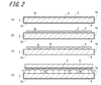
- FIG. 2 is a diagram for explaining an embodiment of the method for manufacturing a semiconductor element of the present disclosure. In the figure, steps (a), (b), (c), and (d), which are manufacturing steps of a semiconductor device, are shown.
- the method for manufacturing a semiconductor element of the embodiment is configured by performing a substrate reuse step of repeating the above-mentioned steps (a) to (d) once or more.
- step (a) shows a mask forming step
- step (b) shows an element forming step
- step (c) shows a mask removing step
- step (d) shows an element separation step.
- the base substrate 1 commonly used in each of the steps (a) to (d) is a first base surface 1a, which is a flat one main surface serving as a starting point for semiconductor crystal growth, and a flat other main surface on the back surface thereof. It has a second base surface 1b which is. At least the surface of the first base surface 1a is covered with a nitride semiconductor.
- the base substrate 1 used in the embodiment is, for example, a GaN substrate cut out from a single crystal ingot of gallium nitride (GaN).
- the GaN substrate may be either an n-type substrate or a p-type substrate in which impurities such as Si are doped in the semiconductor.
- a substrate having an impurity density of about 1 ⁇ 10 19 cm -3 or less can be used.
- a substrate in which a GaN semiconductor layer is formed on the surface of a substrate other than GaN such as a sapphire substrate, a silicon substrate, and a SiC substrate may be used.
- the surface of the base substrate 1 is not limited to the GaN layer, and any substrate made of a GaN-based semiconductor can be used.
- the protective layer 4 may be formed on the second base surface 1b and the substrate end surface 1c of the base substrate 1 located on the opposite side (lower side) of the first base surface 1a, excluding the first base surface 1a which is the starting point of semiconductor crystal growth.
- the protective layer 4 is formed in order to suppress deterioration of the base substrate 1 and decomposition of the nitride semiconductor due to the steps described later.
- the protective layer 4 may be formed of, for example, a layer containing aluminum oxide, alumina, or the like. However, the protective layer 4 may not be provided on the substrate end surface 1c.
- the back surface of the base substrate 1 is gradually thermally decomposed and easily deteriorated. Therefore, a change in the thermal emissivity and an in-plane distribution of the thermal emissivity occur due to alteration of the second base surface 1b, which is the back surface of the base substrate 1. As a result, the growth conditions of the semiconductor crystal tend to deviate from the optimum conditions, which causes a decrease in mass productivity.
- the protective layer 4 By coating the second base surface 1b of the base substrate 1 with the protective layer 4 as in the present embodiment, deterioration of the second base surface 1b of the base substrate 1 is suppressed, and the growth conditions of the semiconductor crystal are stabilized. Mass productivity can be improved.
- the first method for manufacturing a semiconductor element using the base substrate 1 described above includes steps (a) to (d) shown in FIG.
- the deposition suppression mask 2 is formed on the first base surface 1a of the base substrate 1.
- the semiconductor layer 3 is formed on the first base surface 1a of the masked base substrate 1.
- the deposition suppression mask 2 is removed by etching.
- the semiconductor layer 3 is separated from the first base surface 1a of the base substrate 1.
- Step (a) (first time)
- a deposition suppression mask 2 that suppresses the growth of the semiconductor crystal is placed on the first base surface 1a of the base substrate 1 (GaN substrate) in a predetermined pattern. Form into a shape.
- a SiO 2 layer having a thickness of about 100 to 1000 nm is formed as the deposition suppression mask 2.
- silicon oxide (SiO 2 ) which is a material for the deposition suppression mask 2 is laminated on the first base surface 1a by a PCVD (Plasma Chemical Vapor Deposition) method or the like by about 100 to 1000 nm. ..
- SiO 2 layer parts are removed by a photolithography method, HF (hydrofluoric acid) -based wet etching, or dry etching using a fluorine-based gas such as CF 4.
- a predetermined patterned SiO 2 layer can be formed on the first base surface 1a as the deposition suppression mask 2.
- the exposed surface E seen through the band-shaped groove (upward opening) between the mask 2 and the mask 2 is the first crystal growth region where the first base surface 1a described above is exposed, and the subsequent step (b). ), This is the region that is the starting point for the growth of the semiconductor crystal.
- the (11-20) plane orientation of the exposed surface E that is, the opening width or groove width which is the width in the parallel direction (horizontal direction in the drawing) is, for example, 2 to 20 ⁇ m. Further, the width of the deposition suppression mask 2 in the parallel direction in the embodiment is set to, for example, 50 to 200 ⁇ m.
- the relationship between the width of the deposition suppression mask 2 in the parallel direction and the width of the exposed surface E in the parallel direction may be set in consideration of the ratio of the crystal growth rate shown below and the thickness of the semiconductor layer 3 to be grown. That is, the ratio of the crystal growth rate is the crystal growth rate of the semiconductor layer 3 formed in the step (b) in the direction perpendicular to the first base surface 1a of the base substrate 1 and the first base surface of the base substrate 1. It is the ratio with the crystal growth rate in the direction parallel to 1a.
- the mask pattern of the deposition suppression mask 2 may be a band shape or a stripe shape, or a grid shape in which a plurality of band shapes are arranged so as to be orthogonal to each other in the vertical and horizontal directions. Any pattern may be used as long as it is a so-called repeat pattern (pattern) in which openings divided at regular intervals (repeat pitch) are repeated a plurality of times.
- the surface may be roughened by etching or the like.
- the back surface of the semiconductor element S separated by the step (d) can be made uneven, and the first surface 31 of the semiconductor element S (the peeled surface after the semiconductor element S is separated) and the n-type electrode 12 can be formed. , Has the effect of improving ohmic contact and adhesion.
- the edge region of the first base surface 1a of the base substrate 1 in the vicinity of the substrate end surface 1c of the base substrate 1 is also covered with the above-mentioned deposition suppression mask 2 in consideration of the ease of peeling / separation of the semiconductor layer 3 described later. It is covered with.
- the semiconductor layer 3 located near the edge of the base substrate 1 can also be peeled off cleanly and reliably.
- the mask material constituting the deposition suppression mask 2 for example, a material containing silicon oxide such as SiO 2 is used.
- the deposition suppression mask 2 may be any material as long as the semiconductor layer 3 does not grow from the surface of the mask material due to vapor phase growth. Outside those containing silicon oxide, for example, zirconium oxide (ZrO X), titanium oxide (TiO X), it is possible to use an oxide such as aluminum oxide (AlO X).
- a transition metal selected from chromium (Cr), tungsten (W), molybdenum (Mo), tantalum (Ta), niobium (Nb) and the like may be used.
- a method for depositing the mask material a method suitable for the mask material such as thin film deposition, sputtering, and coating curing can be appropriately used.
- Step (b) (first time)
- the semiconductor crystal is grown from the exposed surface E, which is the first crystal growth region, so as to spread over the adjacent deposition suppression mask 2, and the semiconductor layer 3 to be the element is formed.
- the semiconductor layer 3 in the present embodiment is a nitride semiconductor, and by epitaxial growth, the nitride semiconductor is spread from the first base surface 1a beyond the upper edge opening of the groove of the deposition suppression mask 2 and above the deposition suppression mask 2. To grow up to.
- a vapor phase growth method such as a vapor phase growth (MOCVD; Metalorganic Chemical Vapor Deposition) method or a molecular beam vapor phase growth (MBE; Molecular Beam Epitaxy) method can be used.
- the base substrate 1 on which the deposition suppression mask 2 is patterned is inserted into the reaction chamber of the epitaxial device, and hydrogen gas, nitrogen gas, or hydrogen gas, nitrogen gas, or
- the base substrate 1 is heated while supplying a mixed gas of hydrogen and nitrogen and a gas of a group V raw material (containing a group 15 element) such as ammonia to raise the temperature to a predetermined growth temperature, for example, 1050 to 1100 ° C.
- a group III (containing group 13 element) raw material such as trimethylgallium (TMG) is supplied from the exposed surface E which is a crystal growth region.
- TMG trimethylgallium
- the doping amount can be adjusted by supplying a raw material gas such as an n-type impurity such as Si or a p-type impurity such as Mg, and a desired conductive type GaN layer can be obtained. Further, before the growth crystal crosses the upper edge opening of the groove between the deposition suppressing masks 2 or fills the groove, the supply of the raw material is temporarily stopped, the growth of the semiconductor crystal is stopped, and the supply of the raw material is restarted. In addition, a "fragile portion" that facilitates peeling of the semiconductor layer 3 described later may be formed as a partial layer or film.
- the fragile portion for example, when a GaN layer is crystal-grown, GaN, BN, and AlN are formed between the upper semiconductor layer 3 on the opening side and the lower semiconductor layer 3 on the exposed surface E side in the groove. , InN and the like may be formed as a fragile portion.
- these fragile portions When the semiconductor element S is separated / peeled from the base substrate 1 by these fragile portions, stress is concentrated on the fragile portion and cracks are likely to occur, so that the semiconductor element S can be easily separated from the base substrate 1. it can. Further, these fragile portions form an n-type electrode 12 so as to cover the three crystal planes 10a, 10b, 10c of the convex portion 9 which is a part of the first surface 31 of the semiconductor element S, thereby making ohmic contact. Can be improved.
- GaN is laterally grown (ELO; Epiaxial Lateral Over-Growth) starting from the upper surface (surface) of the fragile portion.
- ELO Epiaxial Lateral Over-Growth
- GaN is grown laterally starting from the exposed surface E (first base surface 1a of the base substrate 1) between the masks described above.
- an n + type GaN layer doped with, for example, Si as an n-type impurity is grown in an island shape in the (0001) plane direction.
- the thickness of the n + type GaN layer is, for example, 10 ⁇ m, and the impurity concentration is, for example, 1 ⁇ 10 18 cm -3 .
- the distance between the n + type GaN layer and the n + type GaN layer in the ⁇ 11-20> direction is, for example, about 10 ⁇ m.
- the n + type GaN layer is grown, for example, at a temperature of 1100 ° C. and a pressure of 30 kPa.
- n + type GaN layer is grown, for example, TMG and NH 3 are used as raw material gases, H 2 and N 2 are used as carrier gases, and SiH 4 diluted with nitrogen is used as the n type dopant.
- One island-shaped n + type GaN layer is grown from one striped window.
- the crystal growth conditions are adjusted so that the growth in the vertical direction is promoted, and the n-type GaN layer is grown on the n + -type GaN layer by the MOCVD method.
- the thickness of this n-type GaN layer is, for example, 5 ⁇ m, and the impurity concentration is, for example, 1 ⁇ 10 16 cm -3 .
- the distance between the n-type GaN layer and the entire n-type GaN layer in the ⁇ 11-20> direction is, for example, about 5 ⁇ m.
- the semiconductor layer 3 After the crystal growth surface exceeds the upper edge of the deposition suppression mask 2, the semiconductor layer 3 grows in the lateral direction (horizontal direction in the drawing) along the upper surface of the deposition suppression mask 2. Therefore, the semiconductor layer 3 can be a semiconductor layer suitable for use in a light emitting diode (abbreviated as LED), a laser diode (abbreviated as LD) element, or the like, which has few through dislocations.
- LED light emitting diode
- LD laser diode
- steps (b) are completed after each semiconductor layer 3 that has started to grow from the exposed surface E between the masks comes into contact with the adjacent semiconductor layer 3 or before they overlap each other. Alternatively, they may be brought into contact with each other before being terminated.
- Step (c) (first time) After the above-mentioned steps (b) (first time) are completed, the mask removing step (c) is performed.
- the base substrate 1 is taken out from the vapor phase growth apparatus (epitaxial apparatus), and the deposition suppression mask 2 is removed by using an etchant that does not substantially invade the grown semiconductor layer 3.
- each deposition suppression mask 2 is removed by etching, and the semiconductor layer 3 is placed on the exposed surface E between the deposition suppression mask 2 and the deposition suppression mask 2 adjacent to each other as shown in FIG. 2 (c). It has a substantially T-shaped shape, leaving only the connection portion consisting of a thin semiconductor wall or column. With this shape, the semiconductor layer 3 can be smoothly separated.
- step (d) (first time)
- step (d) which is an element separation step, a support substrate 6 or the like having an adhesive layer 5 made of solder using a material such as AuSn on one surface (second surface 32 in this embodiment) of the semiconductor layer 3 or the like.
- the semiconductor layer 3 is separated from the base substrate 1 by using the members or jigs of the above, and each is used as an individual semiconductor element S.
- the support substrate 6 having the adhesive layer 5 on the lower surface is opposed to the surface (that is, the first base surface 1a) on which the semiconductor layer 3 of the base substrate 1 is formed, and the adhesive layer 5 is formed. Is pressurized and heated on the semiconductor layer 3 to be adhered.
- the separation may be performed by using an adhesive tape such as a dicing tape or a double-sided tape. ..
- the base substrate 1 after the semiconductor element is separated is polished to remove damage during peeling of the semiconductor element S in the epitaxial growth process, which is a mask forming process similar to the first production.
- A a step (b) which is an element forming step, a step (c) which is a mask removing step, and a step (d) which is an element separating step are performed.
- a high-quality semiconductor element S having excellent ohmic contact which is equivalent to that obtained in the first production, can be repeatedly produced using the same base substrate 1.
- Examples of the types of damage include pits due to the reaction between the SiO 2 mask and Ga, formation of the SiO 2 mask, temperature rise, surface roughness of GaN due to the removal step, and dislocations caused by peeling.
- each step (a) to (d) may be repeated by shifting the mask opening without removing the damage.
- FIG. 3 and 4 are enlarged photographs showing the cross-sectional shape of the base substrate 1 near the opening.
- the cross-sectional shape of the opening of the base substrate 1 after the semiconductor element S was peeled off was concave, and the damage depth ⁇ d was 1 ⁇ m or less.
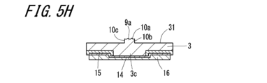
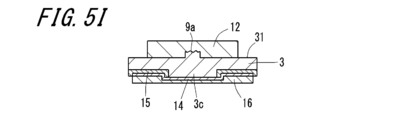
- FIG. 5A to 5K are cross-sectional views schematically showing a manufacturing procedure of the semiconductor laser device of the second embodiment according to the present disclosure.
- FIG. 5A shows a state in which the deposition suppression mask 2 is laminated on the first base surface 1a of the base substrate 1
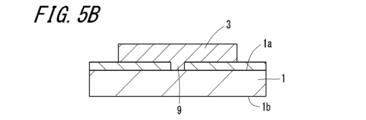
- FIG. 5B shows a state in which the semiconductor layer 3 is formed on the deposition suppression mask 2.
- FIG. 5C shows a state in which the ridge 3c is formed on the semiconductor layer 3
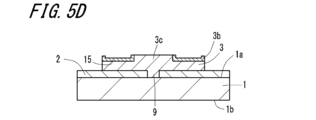
- FIG. 5D shows a state in which the insulating film 15 is formed on the flat surface portion 3b of the semiconductor layer 3 having the ridge 3c.
- FIG. 5A shows a state in which the deposition suppression mask 2 is laminated on the first base surface 1a of the base substrate 1
- FIG. 5B shows a state in which the semiconductor layer 3 is formed on the deposition suppression mask 2.
- FIG. 5C shows a state in which the ridge 3c is formed on the semiconductor layer 3
- FIG. 5D shows a state in which the insulating
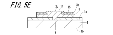
- FIG. 5E shows a state in which the p-type electrode 14 is laminated on the ridge 3c and the insulating film 15, and FIG. 5F shows a state in which the electrode pad 16 is laminated on the p-type electrode 14.
- FIG. 5G shows a state in which the deposition suppression mask 2 is removed
- FIG. 5H shows a state in which the semiconductor laser element separated from the base substrate 1 is turned upside down.
- FIG. 5I shows a state in which the n-type electrode 12 is formed on the first surface 31 of the semiconductor layer 3
- FIG. 5J shows a state in which a pair of resonator surfaces are end-face coated
- FIG. 5K shows the n-type electrode 12.
- FIG. 6 is an enlarged photograph of the semiconductor layer 3 seen from above in FIG. 5H.
- the same reference numerals are given to the parts corresponding to the above-described embodiments, and duplicate description will be omitted.
- the semiconductor laser element which is the semiconductor element of the present embodiment, has a substantially rectangular shape having a length of 50 to 1300 ⁇ m, a width of 30 to 250 ⁇ m, and a height of 5 to 150 ⁇ m, and has two resonator surfaces in the longitudinal direction perpendicular to the paper surface of FIG. 5K. Are formed so as to face each other, and are configured to emit a laser beam from one of the resonator surfaces.
- the base substrate 1 is made of n-type gallium nitride (GaN), and is, for example, a transparent substrate in which the normals of the first base surface 1a and the second base surface 1b have an off angle with respect to the c-axis direction or the c-axis.
- the thickness is about 40 to 600 ⁇ m.
- the base substrate 1 can be formed from a GaN wafer having a diameter of about 2 inches.
- the base substrate 11 may be doped with an n-type dopant such as Si and may have conductivity.
- a deposition suppression mask 2 having a plurality of grooves 2a in a stripe shape is laminated on the first base surface 1a of the base substrate 1, and a nitride semiconductor is epitaxially grown on the deposition suppression mask 2.
- the semiconductor layer 3 is laminated as shown in FIG. 5B.
- a SiO 2 layer having a thickness of about 100 to 1000 nm is formed.
- silicon oxide (SiO 2 ) which is a material for the deposition suppression mask 2 is laminated on the first base surface 1a by a PCVD (Plasma Chemical Vapor Deposition) method or the like by about 100 to 1000 nm. ..
- a predetermined patterned SiO 2 layer can be formed as the deposition suppression mask 2.
- the first base surface 1a is partially exposed from the band-shaped groove 2a of the deposition suppression mask 2, and is a region E that is the starting point for the growth of the semiconductor crystal.
- the semiconductor layer 3 has a ridge 3c on the opposite side of the base substrate 1.
- an insulating film 15 is provided on the flat surface portion 3b of the semiconductor layer 3 excluding the upper surface of the ridge 3c.
- a p-type electrode 14 which is a second electrode is provided on the semiconductor layer 3.
- the insulating film 15 is provided on the semiconductor layer 3 other than the ridge 3c, and at this location, the p-type electrode 14 is provided on the semiconductor layer 3 via the insulating film 15.
- the semiconductor layer 3 and the p-type electrode 14 do not need to be electrically connected to each other on the entire surface, and the portion other than the ridge 3c under the p-type electrode 14 is an insulating film as in the present embodiment. It may be covered with 15.
- the semiconductor layer 3 has a band-shaped convex portion 9 in a region facing the base substrate 1.
- an n-type electrode 12, which is a first electrode is provided on the first surface 31 of the semiconductor layer 3.
- the n-type electrode 12 is provided on the first surface 31 of the semiconductor layer 3 including the convex portion 9.
- the semiconductor layer 3 has a thickness of about 2 to 5 ⁇ m, and has a structure in which thin films of nitride semiconductors are laminated.
- the semiconductor layer 3 includes a first n-type nitride semiconductor layer, a second n-type nitride semiconductor layer, an active layer, a first p-type nitride semiconductor layer, and a second p-type nitride on the first base surface 1a of the base substrate 1.
- the semiconductor layer, the third p-type nitride semiconductor layer, and the fourth p-type nitride semiconductor layer are laminated in this order.
- These semiconductor layers 3 can be represented as a composition formula In x Al y Ga 1-x -y N (0 ⁇ x ⁇ 1-1 ⁇ y ⁇ 1-1 ⁇ x + y ⁇ 1), indium nitride (InN ), Aluminum nitride (AlN), and gallium nitride (GaN) are the main components. Further, as n-type impurities contained in the semiconductor layer 3, silicon (Si), germanium (Ge), tin (Sn), sulfur (S), oxygen (O), titanium (Ti), zinc (Zr), and cadmium ( Cd) and the like can be used.
- the active layer can have, for example, a multiple quantum well structure in which a barrier layer and a well layer are repeatedly laminated by changing the ratio of In and Ga components of InGaN.
- the active layer may or may not contain impurities.
- the third p-type nitride semiconductor layer and the fourth p-type nitride semiconductor layer form ridges 3c formed so as to project in a band shape by etching.
- the width of the ridge 3c is about 2 to 20 ⁇ m, and the height is about ⁇ 1.3 to 0.6 ⁇ m.
- the ridge 3c exists on the entire surface of the semiconductor layer 3 from one resonator surface to the other resonator surface in the length direction. Each of both end faces in the longitudinal direction of the ridge 3c is included in the resonator surface of the semiconductor laser device.
- the mirror layer may be formed of the thin film of.
- the semiconductor layer 3 of the semiconductor laser device is a laminate in which a plurality of semiconductor layers are laminated, and has a protrusion 9 (second region W2) that protrudes from the first region W1.
- It includes a semiconductor layer 3 which is a body, and an n-type electrode 12 located on a first region W1 and a second region W2.
- the first region W1 has a rough surface region a having a surface roughness larger than that of the other regions b in the contact region with the n-type electrode 12.
- the surface roughness can be measured by, for example, an atomic force microscope (AFM).
- another region b is located between the rough surface region a and the convex portion 9.
- the other region b extends in a band shape along the convex portion 9 in the vicinity of the convex portion 9, and the rough surface region a extends in a band shape along the other region b.
- a rough surface region a is the first surface of the semiconductor layer 3 located on the surface of the deposition suppression mask 2 by roughening the surface of at least a part of the deposition suppression mask 2 arranged on the base substrate 1.
- the surface roughness of a part of the region W1 (rough surface region a) can be adjusted. Since the surface roughness of a part of the first region W1 is large, the connection with the electrode 12 can be improved.
- the surface roughness of a part of the first region W1 is large, a crystal plane having a plane orientation different from the (000-1) plane orientation and the (1-100) plane orientation is positioned on the first region W1.
- the surface of the first region W1 can have a crystal plane including a (000-1) plane orientation and a plane orientation different from the (1-100) plane orientation.
- the rough surface region a may have crystal planes such as the A plane (11-20) and the R plane (1-102).
- the area of the crystal plane including the (000-1) plane orientation or the (1-100) plane orientation is the (000-1) plane orientation and (1) plane orientation. -100) It may be smaller than the area of the crystal plane including the plane orientation different from the plane orientation.
- the other regions are The width B1 of the region b is 10% or more and 80% or less of the total width B0, and the width B2 of the rough surface region a is 20% or more and 90% or less of the total width B0.
- the semiconductor layer 3 which is a laminated body is made of a GaN-based semiconductor, and the other region a and the rough surface region b of the first region W1 are the above-mentioned three crystal planes 10a and 10b of the first surface 31.
- Two nitrogen polar planes (hereinafter, also referred to as "N planes") located in the ⁇ 11-20> direction of 10c (the left-right direction in FIG. 5C).
- the surface roughness of the other region b is 0.05 nm or more and less than 1 nm, and the surface roughness of the rough surface region a is 1 nm or more and less than 1000 nm.
- the convex portion 9 has a first convex region 9a located on the semiconductor layer 3 side and a second convex portion 9 located on the base substrate 1 side (tip side of the convex portion 9) with respect to the first convex region 9a. It has a biconvex region 9b.
- the impurity concentration in the second convex region 9b is smaller than the impurity concentration in the first convex region 9a.
- the first convex region 9a may be located closer to the tip of the convex portion 9 than the second convex region 9b.
- These first convex regions 9a and second convex regions 9b form a connecting portion in a connected state.
- Such a convex portion 9 can be formed by separating the semiconductor layer 3 from the base substrate 1 together with a part of the base substrate 1.
- the dislocation density of the second convex region 9b may be smaller than the dislocation density of the first convex region 9a.
- the convex portion 9 is formed by crystal growth of a nitride semiconductor on the exposed surface E of the first base surface 1a of the base substrate 1, and refers to a state in which the first convex region 9a and the second convex region 9b are connected to each other. ..
- the dislocation density of the first convex area 9a for example, 1 ⁇ is 10 4 or more 1 ⁇ 10 7 or less
- the dislocation density of the second convex area 9b for example, 1 ⁇ 10 3 or more 5 ⁇ 10 It is 6 or less.
- the number of dislocation defects in the connecting portion may be larger than that in the second convex region 9b. Further, the number of dislocation defects in the connecting portion may be larger than that in the first convex region 9a.
- the dislocation density can be adjusted by changing the growth conditions during the growth of the semiconductor layer 3. That is, the dislocation density may be higher than the regions located above and below the connection.
- the density of dislocations which are crystal defects of such a semiconductor crystal, can be adjusted by appropriately controlling the growth conditions of the semiconductor layer 3.
- the length of the convex portion 9 of the first convex region 9a in the protruding direction may be larger than the length of the convex portion 9 of the second convex region 9b in the protruding direction. Further, the surface area of the first convex region 9a may be larger than the surface area of the second convex region 9b.
- the entire surface of the first region W1 may be a rough surface, or only a part of the region may be a rough surface. Further, when only a part of the region is a rough surface, the rough surface region a may be located in the vicinity of the convex portion 9. That is, in the parallel direction, the area of the region between the outer edge of the rough surface region a and the convex portion 9 is smaller than the area of the region between the other outer edge of the rough surface region a and the outer edge of the semiconductor layer 3. May be good.
- a plurality of rough surface regions a may be located on both sides of the convex portion 9.
- the convex portion 9 is located between the two rough surface regions a.
- the n-type electrode 12 may be configured to cover only one of the rough surface regions a on both sides of the convex portion 9.
- the configuration in which the semiconductor layer 3 has the strip-shaped convex portion 9 is described, but in other embodiments, instead of the convex portion 9, the first surface 31 is flatter than the first region W1.
- a configuration may be provided in which a recessed band-shaped recess 9'(second region W2) is provided. Even in such a configuration, at least one of the first region W1 and the second region W2 has a crystal plane having a plane orientation different from the (000-1) plane orientation and the (1-100) plane orientation, so that the electrodes It is possible to develop a crystal plane having high ohmic contact with a conductor layer such as the above, and improve the bonding reliability between layers.
- the recess 9' can be formed and the crystal plane 10a can be expressed as shown by the virtual line in FIG.
- the semiconductor element S of the present embodiment has a first surface 31 of the (000-1) plane orientation of the GaN-based semiconductor, which faces the planar first base surface 1a which is one main surface of the base substrate 1.
- the first surface 31 has a flat first region W1 and a second region W2 recessed from the first region W1. Therefore, the first plane 31 has a plurality of crystal planes (second region W2) including plane orientations different from the (000-1) plane, and the ⁇ 11-20> directions of these crystal planes (horizontal direction in FIG. 1). ), It has two nitrogen polar planes (hereinafter, also referred to as “N planes”) 10d and 10e (first region W1). As for the plurality of crystal planes, crystal planes other than the nitrogen polar planes 10d and 10e, for example, the M plane (1-100), the A plane (11-20), and the R plane (1-102) are exposed.
- a semiconductor device having gallium nitride A semiconductor layer having a first surface including a first region and a second region which is a band-shaped convex portion or a concave concave portion protruding from the first region is provided. Of the first plane, at least one of the surfaces of the first region or the second region has a crystal plane containing a plane orientation different from the (000-1) plane orientation and the (1-100) plane orientation.
- the semiconductor element is provided.
- the semiconductor layer further has a second surface facing the first surface.
- a crystal plane having a plane orientation different from the plane orientation facing the plane orientation of the second plane.
- a semiconductor device in which one of the three or more crystal planes of the convex portion is a crystal plane including a (000-1) plane orientation and a (1-100) plane orientation.
- a semiconductor device in which the surface of the first region has a crystal plane having a plane orientation different from that of the surface of the second region.
- a semiconductor device in which the surface of the first region has a crystal plane having the same plane orientation as the surface of the second region.
- a semiconductor device further comprising a first electrode arranged in the first region and the second region of the first surface.
- the first electrode is a semiconductor element which is an n-type electrode.
- the semiconductor layer further has a second surface facing the first surface.
- a semiconductor device further having a second electrode arranged on the second surface.
- a semiconductor device having the first surface having the second region and a plurality of second regions sandwiching the two regions.
- a semiconductor device in which the surfaces of the plurality of second regions have a crystal plane including a (000-1) plane orientation and a plane orientation different from the (1-100) plane orientation.
- a semiconductor device having a crystal plane including a (000-1) plane orientation and a plane orientation different from the (1-100) plane orientation on the surface of the first region.
- a semiconductor device in which the contact region between the first electrode and the first region is larger than the contact region between the first electrode and the second region.
- the area of the crystal plane including the (000-1) plane orientation or the (1-100) plane orientation is the (000-1) plane orientation and (1) plane orientation. -100) It is smaller than the area of the crystal plane including the plane orientation different from the plane orientation.
- the area of the crystal plane including the (000-1) plane orientation or the (1-100) plane orientation is the (000-1) plane orientation and (1) plane orientation. -100) It is smaller than the area of the crystal plane including the plane orientation different from the plane orientation.
- a method for manufacturing a semiconductor element in which when the semiconductor layer is peeled off from the substrate, the semiconductor layer is peeled off together with a part of the substrate connected to the semiconductor layer.
- (21) A method for manufacturing a semiconductor element, in which the semiconductor layer is peeled off so that a part of the semiconductor layer remains on the substrate when the semiconductor layer is peeled off from the substrate.
- a step of forming a mask on the first surface of the substrate before forming the semiconductor layer while exposing a region serving as a starting point of growth of the semiconductor layer is further provided.
- a semiconductor device having gallium nitride A semiconductor layer epitaxially grown from a substrate, which has a first surface including a first region and a second region adjacent to the first region, is provided. The second region is a peeling surface formed when separated from the substrate.
- a semiconductor device in which the peeled surface has a crystal plane including a (000-1) plane orientation and a plane orientation different from the (1-100) plane orientation.
- the convex portion has a connecting portion in which the first convex region and the second convex region are connected.
- the convex portion has a connecting portion in which the first convex region and the second convex region are connected.
- the convex portion is a semiconductor device having a first convex region and a second convex region having a dislocation density lower than that of the first convex region.
- the convex portion has a connecting portion in which the first convex region and the second convex region are connected.
- the convex portion 7, the first convex region and the second convex region are connected to each other.
- the semiconductor element of the present disclosure since the semiconductor element has flat surfaces 10a to 10e having high ohmic contact, the ohmic contact between the semiconductor layer 3 and the insulating film 15 and the semiconductor layer 3 and the n-type electrode 12 is improved. High junction reliability can be obtained without the need for a step of performing a process for performing the above, and the semiconductor element can be realized as, for example, a semiconductor laser element. As a result, it is possible to improve the productivity of the semiconductor element and provide the semiconductor element having excellent mass productivity.
- the method for manufacturing a semiconductor device of the present disclosure it is possible to realize a semiconductor device having a surface having high ohmic contact without increasing the number of steps. This makes it possible to facilitate mass productivity of semiconductor devices having high junction reliability.
- Base substrate 1a 1st base surface 1b 2nd base surface 1d Edge 2 Accumulation suppression mask 3 Semiconductor layer 3a Remaining semiconductor layer 3b Flat surface 3c Ridge 4 Protective layer 5 Adhesive layer 6 Support substrate 9 Connection 9a 1st convex region 9b Second convex region 10a, 10b, 10c Multiple crystal planes 12 n-type electrodes 14 p-type electrodes 15 Insulation layer 16 Mounting board 31 First surface 32 Second surface E Exposed surface S Semiconductor element
Landscapes
- Physics & Mathematics (AREA)
- Condensed Matter Physics & Semiconductors (AREA)
- General Physics & Mathematics (AREA)
- Electromagnetism (AREA)
- Optics & Photonics (AREA)
- Semiconductor Lasers (AREA)
- Led Devices (AREA)
- Electrodes Of Semiconductors (AREA)
- Recrystallisation Techniques (AREA)
Priority Applications (5)
| Application Number | Priority Date | Filing Date | Title |
|---|---|---|---|
| US17/771,149 US20220416015A1 (en) | 2019-10-29 | 2020-10-29 | Semiconductor element and method for manufacturing semiconductor element |
| CN202080074286.1A CN114600248B (zh) | 2019-10-29 | 2020-10-29 | 半导体元件和半导体元件的制造方法 |
| EP20881210.7A EP4053881B1 (en) | 2019-10-29 | 2020-10-29 | Semiconductor element and method for producing semiconductor element |
| JP2021553694A JP7343607B2 (ja) | 2019-10-29 | 2020-10-29 | 半導体素子および半導体素子の製造方法 |
| JP2023141584A JP7645319B2 (ja) | 2019-10-29 | 2023-08-31 | 半導体素子 |
Applications Claiming Priority (2)
| Application Number | Priority Date | Filing Date | Title |
|---|---|---|---|
| JP2019196342 | 2019-10-29 | ||
| JP2019-196342 | 2019-10-29 |
Publications (1)
| Publication Number | Publication Date |
|---|---|
| WO2021085556A1 true WO2021085556A1 (ja) | 2021-05-06 |
Family
ID=75715190
Family Applications (1)
| Application Number | Title | Priority Date | Filing Date |
|---|---|---|---|
| PCT/JP2020/040692 Ceased WO2021085556A1 (ja) | 2019-10-29 | 2020-10-29 | 半導体素子および半導体素子の製造方法 |
Country Status (5)
| Country | Link |
|---|---|
| US (1) | US20220416015A1 (https=) |
| EP (1) | EP4053881B1 (https=) |
| JP (2) | JP7343607B2 (https=) |
| CN (1) | CN114600248B (https=) |
| WO (1) | WO2021085556A1 (https=) |
Cited By (4)
| Publication number | Priority date | Publication date | Assignee | Title |
|---|---|---|---|---|
| JPWO2023002865A1 (https=) * | 2021-07-21 | 2023-01-26 | ||
| WO2023145799A1 (ja) * | 2022-01-27 | 2023-08-03 | 京セラ株式会社 | 半導体基板の製造方法および製造装置、並びに制御装置 |
| WO2025164326A1 (ja) * | 2024-01-31 | 2025-08-07 | 京セラ株式会社 | 光半導体素子、半導体基板、半導体基板の製造方法、光半導体素子の製造方法 |
| WO2025216274A1 (ja) * | 2024-04-10 | 2025-10-16 | 京セラ株式会社 | 半導体基板およびその製造方法 |
Families Citing this family (1)
| Publication number | Priority date | Publication date | Assignee | Title |
|---|---|---|---|---|
| WO2025182818A1 (ja) * | 2024-02-29 | 2025-09-04 | 京セラ株式会社 | 半導体基板およびその製造方法、発光素子およびその製造方法、電子機器 |
Citations (6)
| Publication number | Priority date | Publication date | Assignee | Title |
|---|---|---|---|---|
| JP2003218389A (ja) * | 2002-01-18 | 2003-07-31 | Sony Corp | 半導体発光素子及びその製造方法 |
| JP2007189135A (ja) * | 2006-01-16 | 2007-07-26 | Sony Corp | GaN系半導体発光素子及びその製造方法 |
| JP2008153286A (ja) * | 2006-12-14 | 2008-07-03 | Rohm Co Ltd | 窒化物半導体積層構造および窒化物半導体装置、ならびに窒化物半導体積層構造の製造方法 |
| JP2011066398A (ja) | 2009-08-20 | 2011-03-31 | Pawdec:Kk | 半導体素子およびその製造方法 |
| JP2012060023A (ja) * | 2010-09-10 | 2012-03-22 | Sony Corp | 半導体発光素子およびその製造方法 |
| JP2012114263A (ja) * | 2010-11-25 | 2012-06-14 | Pawdec:Kk | 半導体素子およびその製造方法 |
Family Cites Families (19)
| Publication number | Priority date | Publication date | Assignee | Title |
|---|---|---|---|---|
| JP3800146B2 (ja) * | 1997-06-30 | 2006-07-26 | 日亜化学工業株式会社 | 窒化物半導体素子の製造方法 |
| JP4060511B2 (ja) * | 2000-03-28 | 2008-03-12 | パイオニア株式会社 | 窒化物半導体素子の分離方法 |
| JP5217077B2 (ja) * | 2004-02-20 | 2013-06-19 | 日亜化学工業株式会社 | 窒化物半導体素子及び窒化物半導体基板の製造方法、並びに窒化物半導体素子の製造方法 |
| JP4610244B2 (ja) * | 2004-06-28 | 2011-01-12 | 京セラ株式会社 | 弾性表面波装置の製造方法 |
| FI20045482A0 (fi) * | 2004-12-14 | 2004-12-14 | Optogan Oy | Matalamman dislokaatiotiheyden omaava puolijohdesubstraatti, ja menetelmä sen valmistamiseksi |
| CN100477425C (zh) * | 2005-05-19 | 2009-04-08 | 松下电器产业株式会社 | 氮化物半导体装置及其制造方法 |
| JPWO2009118979A1 (ja) * | 2008-03-28 | 2011-07-21 | パナソニック株式会社 | 窒化物半導体発光装置 |
| JP2009286652A (ja) * | 2008-05-28 | 2009-12-10 | Sumitomo Electric Ind Ltd | Iii族窒化物結晶、iii族窒化物結晶基板および半導体デバイスの製造方法 |
| JP5298889B2 (ja) * | 2009-01-29 | 2013-09-25 | 日亜化学工業株式会社 | 窒化物半導体素子 |
| RU2459691C2 (ru) * | 2010-11-29 | 2012-08-27 | Юрий Георгиевич Шретер | Способ отделения поверхностного слоя полупроводникового кристалла (варианты) |
| KR20150072066A (ko) * | 2013-12-19 | 2015-06-29 | 서울바이오시스 주식회사 | 반도체 성장용 템플릿, 성장 기판 분리 방법 및 이를 이용한 발광소자 제조 방법 |
| JP6135559B2 (ja) * | 2014-03-10 | 2017-05-31 | ソニー株式会社 | 半導体発光素子および半導体発光素子の製造方法ならびに半導体素子 |
| WO2017163548A1 (ja) * | 2016-03-24 | 2017-09-28 | 日本碍子株式会社 | 種結晶基板の製造方法、13族元素窒化物結晶の製造方法および種結晶基板 |
| EP3682465A4 (en) * | 2017-09-15 | 2021-06-02 | The Regents of The University of California | METHOD OF REMOVING A SUBSTRATE USING A SPREADING TECHNIQUE |
| CN108461555A (zh) * | 2018-02-05 | 2018-08-28 | 宇泰(江西)新能源有限公司 | 一种具有表面织构结构的单晶硅光伏电池 |
| CN112204754B (zh) * | 2018-05-30 | 2024-08-13 | 加利福尼亚大学董事会 | 从半导体衬底移除半导体层的方法 |
| JP6595676B1 (ja) * | 2018-08-29 | 2019-10-23 | 株式会社サイオクス | 窒化物半導体基板の製造方法、窒化物半導体基板および積層構造体 |
| US11245051B2 (en) * | 2018-10-12 | 2022-02-08 | Boe Technology Group Co., Ltd. | Micro light emitting diode apparatus and fabricating method thereof |
| EP3912184A4 (en) * | 2019-01-16 | 2022-03-02 | The Regents of the University of California, A California Corporation | PROCEDURE FOR REMOVAL OF DEVICES USING A DIG |
-
2020
- 2020-10-29 EP EP20881210.7A patent/EP4053881B1/en active Active
- 2020-10-29 US US17/771,149 patent/US20220416015A1/en active Pending
- 2020-10-29 WO PCT/JP2020/040692 patent/WO2021085556A1/ja not_active Ceased
- 2020-10-29 JP JP2021553694A patent/JP7343607B2/ja active Active
- 2020-10-29 CN CN202080074286.1A patent/CN114600248B/zh active Active
-
2023
- 2023-08-31 JP JP2023141584A patent/JP7645319B2/ja active Active
Patent Citations (6)
| Publication number | Priority date | Publication date | Assignee | Title |
|---|---|---|---|---|
| JP2003218389A (ja) * | 2002-01-18 | 2003-07-31 | Sony Corp | 半導体発光素子及びその製造方法 |
| JP2007189135A (ja) * | 2006-01-16 | 2007-07-26 | Sony Corp | GaN系半導体発光素子及びその製造方法 |
| JP2008153286A (ja) * | 2006-12-14 | 2008-07-03 | Rohm Co Ltd | 窒化物半導体積層構造および窒化物半導体装置、ならびに窒化物半導体積層構造の製造方法 |
| JP2011066398A (ja) | 2009-08-20 | 2011-03-31 | Pawdec:Kk | 半導体素子およびその製造方法 |
| JP2012060023A (ja) * | 2010-09-10 | 2012-03-22 | Sony Corp | 半導体発光素子およびその製造方法 |
| JP2012114263A (ja) * | 2010-11-25 | 2012-06-14 | Pawdec:Kk | 半導体素子およびその製造方法 |
Cited By (6)
| Publication number | Priority date | Publication date | Assignee | Title |
|---|---|---|---|---|
| JPWO2023002865A1 (https=) * | 2021-07-21 | 2023-01-26 | ||
| WO2023145799A1 (ja) * | 2022-01-27 | 2023-08-03 | 京セラ株式会社 | 半導体基板の製造方法および製造装置、並びに制御装置 |
| JPWO2023145799A1 (https=) * | 2022-01-27 | 2023-08-03 | ||
| JP7745660B2 (ja) | 2022-01-27 | 2025-09-29 | 京セラ株式会社 | 半導体基板の製造方法、半導体基板の製造装置 |
| WO2025164326A1 (ja) * | 2024-01-31 | 2025-08-07 | 京セラ株式会社 | 光半導体素子、半導体基板、半導体基板の製造方法、光半導体素子の製造方法 |
| WO2025216274A1 (ja) * | 2024-04-10 | 2025-10-16 | 京セラ株式会社 | 半導体基板およびその製造方法 |
Also Published As
| Publication number | Publication date |
|---|---|
| EP4053881B1 (en) | 2024-10-09 |
| CN114600248A (zh) | 2022-06-07 |
| EP4053881A4 (en) | 2023-02-01 |
| JP7343607B2 (ja) | 2023-09-12 |
| JP2023162378A (ja) | 2023-11-08 |
| US20220416015A1 (en) | 2022-12-29 |
| JPWO2021085556A1 (https=) | 2021-05-06 |
| EP4053881A1 (en) | 2022-09-07 |
| CN114600248B (zh) | 2025-04-22 |
| JP7645319B2 (ja) | 2025-03-13 |
Similar Documents
| Publication | Publication Date | Title |
|---|---|---|
| US12205847B2 (en) | Method of removing a substrate with a cleaving technique | |
| JP4513446B2 (ja) | 半導体結晶の結晶成長方法 | |
| JP7343607B2 (ja) | 半導体素子および半導体素子の製造方法 | |
| US20240072198A1 (en) | Semiconductor substrate, semiconductor device, and electronic device | |
| JP7776330B2 (ja) | エピタキシャル横方向過成長を用いた非極性及び半極性デバイス作成方法 | |
| JP6704387B2 (ja) | 窒化物半導体成長用基板及びその製造方法、並びに半導体デバイス及びその製造方法 | |
| WO2014021259A1 (ja) | 窒化物半導体素子構造体とその製造方法 | |
| EP2239790A9 (en) | Method for manufacturing light emitting device | |
| JP5140962B2 (ja) | 窒化物半導体基板の製造方法 | |
| JP5834952B2 (ja) | 窒化物半導体基板の製造方法 | |
| JP3698061B2 (ja) | 窒化物半導体基板及びその成長方法 | |
| JP3555657B2 (ja) | 低欠陥窒化物半導体基板及びその製造方法 | |
| KR101116905B1 (ko) | 질화물 반도체 결정 성장 방법 | |
| JP4232326B2 (ja) | 低欠陥窒化物半導体の成長方法 | |
| JP5003719B2 (ja) | 半導体素子及び結晶成長基板 | |
| JP5454647B2 (ja) | 窒化物半導体基板の製造方法、窒化物半導体基板及び発光素子 | |
| US20240313151A1 (en) | Semiconductor device manufacturing method and manufacturing apparatus, semiconductor device and electronic device | |
| JP3823781B2 (ja) | 窒化物半導体基板およびその製造方法 | |
| JP2003243776A (ja) | 支持基板の剥離方法 | |
| JP2003037066A (ja) | 窒化物半導体基板、及びその成長方法 |
Legal Events
| Date | Code | Title | Description |
|---|---|---|---|
| 121 | Ep: the epo has been informed by wipo that ep was designated in this application |
Ref document number: 20881210 Country of ref document: EP Kind code of ref document: A1 |
|
| ENP | Entry into the national phase |
Ref document number: 2021553694 Country of ref document: JP Kind code of ref document: A |
|
| NENP | Non-entry into the national phase |
Ref country code: DE |
|
| ENP | Entry into the national phase |
Ref document number: 2020881210 Country of ref document: EP Effective date: 20220530 |
|
| WWG | Wipo information: grant in national office |
Ref document number: 202080074286.1 Country of ref document: CN |