WO2021079812A1 - 接続体の製造方法、異方性導電接合材料、及び接続体 - Google Patents
接続体の製造方法、異方性導電接合材料、及び接続体 Download PDFInfo
- Publication number
- WO2021079812A1 WO2021079812A1 PCT/JP2020/038842 JP2020038842W WO2021079812A1 WO 2021079812 A1 WO2021079812 A1 WO 2021079812A1 JP 2020038842 W JP2020038842 W JP 2020038842W WO 2021079812 A1 WO2021079812 A1 WO 2021079812A1
- Authority
- WO
- WIPO (PCT)
- Prior art keywords
- solder particles
- anisotropic conductive
- conductive bonding
- electronic component
- temperature
- Prior art date
- Legal status (The legal status is an assumption and is not a legal conclusion. Google has not performed a legal analysis and makes no representation as to the accuracy of the status listed.)
- Ceased
Links
Images


Classifications
-
- C—CHEMISTRY; METALLURGY
- C09—DYES; PAINTS; POLISHES; NATURAL RESINS; ADHESIVES; COMPOSITIONS NOT OTHERWISE PROVIDED FOR; APPLICATIONS OF MATERIALS NOT OTHERWISE PROVIDED FOR
- C09J—ADHESIVES; NON-MECHANICAL ASPECTS OF ADHESIVE PROCESSES IN GENERAL; ADHESIVE PROCESSES NOT PROVIDED FOR ELSEWHERE; USE OF MATERIALS AS ADHESIVES
- C09J163/00—Adhesives based on epoxy resins; Adhesives based on derivatives of epoxy resins
-
- C—CHEMISTRY; METALLURGY
- C09—DYES; PAINTS; POLISHES; NATURAL RESINS; ADHESIVES; COMPOSITIONS NOT OTHERWISE PROVIDED FOR; APPLICATIONS OF MATERIALS NOT OTHERWISE PROVIDED FOR
- C09J—ADHESIVES; NON-MECHANICAL ASPECTS OF ADHESIVE PROCESSES IN GENERAL; ADHESIVE PROCESSES NOT PROVIDED FOR ELSEWHERE; USE OF MATERIALS AS ADHESIVES
- C09J11/00—Features of adhesives not provided for in group C09J9/00, e.g. additives
- C09J11/02—Non-macromolecular additives
- C09J11/04—Non-macromolecular additives inorganic
-
- C—CHEMISTRY; METALLURGY
- C09—DYES; PAINTS; POLISHES; NATURAL RESINS; ADHESIVES; COMPOSITIONS NOT OTHERWISE PROVIDED FOR; APPLICATIONS OF MATERIALS NOT OTHERWISE PROVIDED FOR
- C09J—ADHESIVES; NON-MECHANICAL ASPECTS OF ADHESIVE PROCESSES IN GENERAL; ADHESIVE PROCESSES NOT PROVIDED FOR ELSEWHERE; USE OF MATERIALS AS ADHESIVES
- C09J11/00—Features of adhesives not provided for in group C09J9/00, e.g. additives
- C09J11/02—Non-macromolecular additives
- C09J11/06—Non-macromolecular additives organic
-
- C—CHEMISTRY; METALLURGY
- C09—DYES; PAINTS; POLISHES; NATURAL RESINS; ADHESIVES; COMPOSITIONS NOT OTHERWISE PROVIDED FOR; APPLICATIONS OF MATERIALS NOT OTHERWISE PROVIDED FOR
- C09J—ADHESIVES; NON-MECHANICAL ASPECTS OF ADHESIVE PROCESSES IN GENERAL; ADHESIVE PROCESSES NOT PROVIDED FOR ELSEWHERE; USE OF MATERIALS AS ADHESIVES
- C09J7/00—Adhesives in the form of films or foils
- C09J7/30—Adhesives in the form of films or foils characterised by the adhesive composition
- C09J7/35—Heat-activated
-
- C—CHEMISTRY; METALLURGY
- C09—DYES; PAINTS; POLISHES; NATURAL RESINS; ADHESIVES; COMPOSITIONS NOT OTHERWISE PROVIDED FOR; APPLICATIONS OF MATERIALS NOT OTHERWISE PROVIDED FOR
- C09J—ADHESIVES; NON-MECHANICAL ASPECTS OF ADHESIVE PROCESSES IN GENERAL; ADHESIVE PROCESSES NOT PROVIDED FOR ELSEWHERE; USE OF MATERIALS AS ADHESIVES
- C09J9/00—Adhesives characterised by their physical nature or the effects produced, e.g. glue sticks
- C09J9/02—Electrically-conducting adhesives
-
- H—ELECTRICITY
- H01—ELECTRIC ELEMENTS
- H01B—CABLES; CONDUCTORS; INSULATORS; SELECTION OF MATERIALS FOR THEIR CONDUCTIVE, INSULATING OR DIELECTRIC PROPERTIES
- H01B1/00—Conductors or conductive bodies characterised by the conductive materials; Selection of materials as conductors
- H01B1/20—Conductive material dispersed in non-conductive organic material
- H01B1/22—Conductive material dispersed in non-conductive organic material the conductive material comprising metals or alloys
-
- H—ELECTRICITY
- H01—ELECTRIC ELEMENTS
- H01R—ELECTRICALLY-CONDUCTIVE CONNECTIONS; STRUCTURAL ASSOCIATIONS OF A PLURALITY OF MUTUALLY-INSULATED ELECTRICAL CONNECTING ELEMENTS; COUPLING DEVICES; CURRENT COLLECTORS
- H01R11/00—Individual connecting elements providing two or more spaced connecting locations for conductive members which are, or may be, thereby interconnected, e.g. end pieces for wires or cables supported by the wire or cable and having means for facilitating electrical connection to some other wire, terminal, or conductive member, blocks of binding posts
- H01R11/01—Individual connecting elements providing two or more spaced connecting locations for conductive members which are, or may be, thereby interconnected, e.g. end pieces for wires or cables supported by the wire or cable and having means for facilitating electrical connection to some other wire, terminal, or conductive member, blocks of binding posts characterised by the form or arrangement of the conductive interconnection between the connecting locations
Definitions
- the present invention relates to a method for manufacturing a connector for mounting a semiconductor chip (element), an anisotropic conductive bonding material, and a connector.
- Flip chip mounting is one of the methods for mounting semiconductor chips (elements). Flip chip mounting can reduce the mounting area as compared with wire bonding, and can mount small and thin semiconductor chips.
- Patent Document 1 describes that a plurality of parts are collectively mounted on a wiring board or the like by reflow using a solder paste containing solder particles, a thermosetting resin binder, and a flux component.
- solder paste of Patent Document 1 contains a large amount of solder particles in order to melt and integrate the solder particles, and it is difficult to join electronic components provided with fine pitch electrodes.
- This technology has been proposed in view of such conventional circumstances, and is a method for manufacturing a connector capable of bonding electronic components provided with fine pitch electrodes, an anisotropic conductive bonding material, and a connector. I will provide a.
- the present inventor has found that the above object can be achieved by using an anisotropic conductive bonding material that exhibits conductivity only in the direction in which the conductive particles are sandwiched, and completes the present invention. I arrived.
- the solder particles are dispersed in a heat-curable insulating binder, and the minimum melt viscosity reaching temperature lower than the melting point of the solder particles and the melting point of the solder particles are obtained.
- An anisotropic conductive bonding material having a higher curing temperature is interposed between the electrodes of the first electronic component and the electrodes of the second electronic component, and the electrodes of the first electronic component and the second electronic component are interposed.
- the electrodes of the electronic parts of the above are joined with no load using a reflow furnace, and the peak temperature of the reflow furnace is 10 degrees or more higher than the curing temperature of the anisotropic conductive bonding material.
- the solder particles are dispersed in a thermosetting insulating binder, and the minimum melt viscosity reaching temperature lower than the melting point of the solder particles and the solder particles have a minimum melt viscosity reaching temperature. It has a curing temperature higher than its melting point.
- the electrode of the first electronic component and the electrode of the second electronic component are bonded by using the above-mentioned anisotropic conductive bonding material.
- the insulating binder is melted by heating and the binder is cured in a state where the solder particles are sandwiched between the electrodes, it is possible to join electronic components having fine pitch electrodes.
- FIG. 1 is a cross-sectional view schematically showing a part of the joining process.
- FIG. 2 is a cross-sectional view showing a configuration example of the LED mounting body.
- FIG. 3 is a cross-sectional view schematically showing a part of an anisotropic conductive bonding film to which the present technology is applied.
- FIG. 4 is a graph showing the temperature profile of reflow.
- FIG. 5 is a graph showing the measurement results of differential scanning calorimetry (DSC) of the anisotropic conductive bonded film of Example 1.
- FIG. 6 is a photomicrograph when observing the solder bonding state on the substrate side after peeling off the LED chip of Example 1.
- the solder particles are dispersed in a thermosetting insulating binder, and the minimum melt viscosity reaching temperature lower than the melting point of the solder particles and higher than the melting point of the solder particles are higher.
- An anisotropic conductive bonding material having a curing temperature is interposed between the electrodes of the first electronic component and the electrodes of the second electronic component, and the electrodes of the first electronic component and the electrodes of the second electronic component are interposed. Is bonded using a reflow furnace with no load, and the peak temperature of the reflow furnace is 10 degrees or more higher than the curing temperature of the anisotropic conductive bonding material.
- the temperature at which the minimum melt viscosity of the anisotropic conductive bonding material is reached is, for example, a measurement pressure of 5 g, a temperature range of 30 to 200 ° C., and a temperature rise rate of 10 ° C. using a rotary leometer (manufactured by TA instrument).
- the curing temperature of the anisotropic conductive bonding material is the heat generated by measuring 5 mg or more of the sample with an aluminum pan by differential thermal analysis (DSC) under the conditions of a temperature range of 30 to 250 ° C. and a heating rate of 10 ° C./min. It is the peak temperature.
- the connecting body is one in which two materials or members are electrically connected.
- joining is the joining of two materials or members. No load means that there is no mechanical pressurization.
- the first electronic component may be one provided with wiring (conducting material) such as LED (Light Emitting Diode), driver IC (Integrated Circuit), flexible substrate (FPC: Flexible Printed Circuits, resin molded component, etc.). Of these, chips such as LEDs and driver ICs (for example, semiconductor elements) are preferable.
- a terminal corresponding to at least a part of the terminal of the first electronic component is provided.
- a substrate so-called printed wiring board: PWB
- PWB printed wiring board
- a rigid substrate or glass may be used. Examples include substrates such as substrates, flexible printed circuits (FPCs), ceramic substrates, and plastic substrates.
- the same components may be laminated and connected. The number of these layers hinders the connection. If not, there is no particular limitation. The same applies to the case where a large number of dissimilar parts are laminated.
- the electrodes (electrode arrangement, electrode group) provided on the first electronic component and the second electronic component are opposed to each other. It is provided so as to be anisotropically connected, and electrodes (electrode arrangement, electrode group) may be provided so that a plurality of first electronic components are mounted on one second electronic component. It is desirable that the above-mentioned electronic components have heat resistance in the reflow process.
- the connector in this embodiment is connected by solder particles, which are widely used in BGA (Ball grid array) and the like, and has high connection reliability. Therefore, sensor devices, in-vehicle devices, and IoT (Internet of Things) ) It can be applied to many applications such as equipment.
- the anisotropic conductive bonding material may be either a film-shaped anisotropic conductive bonding film or a paste-shaped anisotropic conductive bonding paste. Further, the anisotropic conductive bonding paste may be formed into a film at the time of connection, or may be formed into a form similar to a film by mounting a component.
- anisotropic conductive bonding paste it suffices if a predetermined amount can be uniformly applied onto the substrate. For example, application methods such as dispensing, stamping, and screen printing can be used, and the paste may be dried if necessary. Good.
- an anisotropic conductive bonding film it is particularly preferable because not only the amount of the anisotropic conductive bonding material can be made uniform depending on the film thickness, but also the tact can be shortened because it can be laminated on the substrate at once. .. In addition, since it is easy to handle by forming it into a film in advance, it can be expected that work efficiency will be improved.
- solder particles are dispersed in a heat-curable insulating binder, and a minimum melt viscosity reaching temperature lower than the melting point of the solder particles and a curing temperature higher than the melting point of the solder particles are set.
- a plurality of parts may be mounted at once.
- the step of providing the anisotropic conductive bonding material may be a step of forming a film on the substrate before connecting the anisotropic conductive bonding paste, as used in the conventional anisotropic conductive film. It may be a temporary sticking step of sticking an anisotropic conductive bonding film on a substrate at a low temperature and a low pressure, or a laminating step of laminating an anisotropic conductive bonding film on a substrate.
- the anisotropic conductive bonding film can be provided on the substrate under known usage conditions. In this case, only minimal changes such as installation and change of tools from the conventional device are required, which is economically advantageous.
- the anisotropic conductive bonding film is laminated on the substrate using a pressure type laminator.
- the laminating step may be a vacuum pressurization type.
- the width of the film is restricted by the tool width, but in the laminating process, the heating-pressing tool is not used, so it is relatively wide. It can be expected that the width can be mounted all at once.
- one anisotropic conductive bonding film may be laminated on one substrate.
- the vertical movement of the heat-bonding tool and the transfer of the anisotropic conductive bonding film are not performed a plurality of times, so that the time required for the step of providing the anisotropic conductive bonding material can be shortened.
- the thickness of the anisotropic bonding material between the electrode of the LED element and the electrode of the substrate is approximated to the average particle size of the solder particles.
- the lower limit of the thickness of the anisotropic bonding material is 50% or more, preferably 80% or more, more preferably 90% or more of the average particle size of the solder particles. If the thickness of the anisotropic bonding material is too thin, the solder particles can be easily sandwiched between the electrodes, but there is a risk that the difficulty of forming the solder particles into a film will increase.
- the upper limit of the thickness of the anisotropic bonding material is 300% or less, preferably 200% or less, and more preferably 150% or less of the average particle size of the solder particles. If the thickness of the anisotropic bonding material is too thick, the bonding may be hindered.
- the average particle size obtained from the observed image or the image-type particle size distribution measuring device can be the average value of the maximum lengths of the particles.
- the particle size (D50) and the arithmetic mean diameter (volume basis) at which the cumulative frequency in the particle size distribution simply obtained by the laser diffraction / scattering method is 50% are 50%.
- the manufacturer value such as (preferably) can be used.
- each LED element has, for example, a first conductive type electrode and a second conductive type electrode on one side, and is arranged on an electrode of a substrate 30 corresponding to the first conductive type electrode and the second conductive type electrode.
- the thickness of the anisotropic bonding material between the electrode of the LED element and the electrode of the substrate was made to be close to the average particle size of the solder particles.
- the thickness of the anisotropic bonding material may be approximated to the average particle size of the solder particles by pressurization.
- the thickness of the anisotropic bonding material between the electrode of the LED element and the electrode of the substrate is applied by pressurizing from the side of the first electronic component mounted on the second electronic component. Is approximated to the average particle size of the solder particles.
- the thickness of the anisotropic bonding material is too large, it may interfere with pressurization, so it can be said that it is preferable to set the thickness to the above-mentioned upper limit.
- Approximate to the average particle size means that the maximum diameter of the solder particles is theoretically the thickness of the anisotropic connecting material after this pressurization step, so the thickness of the anisotropic connecting material is the maximum diameter of the solder particles. It may be considered to be equivalent, and if thickness variation is taken into consideration, it may be 130% or less, preferably 120% or less of the maximum diameter of the solder particles.
- the lower limit of the pressure in the pressurizing step is preferably 0.2 MPa or more, more preferably 0.4 MPa or more, and the upper limit of the pressure in the pressurizing step may be 2.0 MPa or less, preferably 1. It is 0 MPa or less, more preferably 0.8 MPa or less. Since the upper limit and the lower limit may vary depending on the specifications of the device, the upper limit and the lower limit are not limited to the above numerical range as long as the purpose of pushing the resin to the solder particle size can be achieved.
- FIG. 1 is a cross-sectional view schematically showing a part of the joining process.
- the electrodes 11 and 12 of the LED element 10 and the electrodes 21 and 21 of the substrate 20 are heat-bonded with no load.
- Examples of the method of heat-joining with no load without mechanical pressurization include atmospheric pressure reflow, vacuum reflow, atmospheric pressure oven, autoclave (pressurized oven), etc. Among these, the method is included in the joint. It is preferable to use a vacuum reflow, an autoclave, or the like that can eliminate air bubbles. Since no load is applied, unnecessary resin flow is not generated as compared with the anisotropic conductive connection using a general heating and pressurizing tool, so that the effect of suppressing the entrainment of air bubbles can be expected.
- the peak temperature in the reflow furnace is required to be 10 ° C. or higher than the curing temperature of the anisotropic conductive bonding material, preferably 150 ° C. or higher and 250 ° C. or lower, more preferably 160 ° C. or higher and 230 ° C. or lower, and further preferably 170 ° C. or higher.
- Main heating is performed at ° C. or higher and 210 ° C. or lower.
- solder bonding means connecting the electrodes of opposing electronic components by melting the solder.
- thermosetting resin In the reflow furnace, the thermosetting resin is melted by heating, the solder particles 31 are sandwiched between the electrodes by the weight of the LED element 10, the solder particles 31 are melted by the main heating which is equal to or higher than the solder melting point, and the solder wets and spreads on the electrodes. By cooling, the electrodes of the LED element 10 and the electrodes of the substrate 20 are joined.
- the reflow may include a step of maintaining a constant temperature (keeping step) in addition to a step of raising the temperature and a step of lowering the temperature. There may be a peak step at the highest temperature, and the step may be included in the middle of raising or lowering the temperature.
- the temperature raising step may be two steps: a step of melting the binder (example: up to 120 ° C. in FIG. 4) and a step of melting and spreading the solder particles (example: 120 to 175 ° C. in FIG. 4). .. Therefore, the heating rate may be 10 to 120 ° C./min or 20 to 100 ° C./min as an example.
- the maintenance time of the keeping step (eg, 175 to 180 ° C. in FIG. 4) is also a step of curing the binder. This temperature is, for example, a temperature of 160 to 230 ° C., and may have a difference of about 5 to 10 ° C., and may be the same as the peak temperature.
- the life performance of the binder will deteriorate and handling will be hindered. Therefore, it is 0.5 min or more, preferably 0.75 min or more. If it is too long, the production efficiency will deteriorate. Therefore, it is 5 min or less, preferably 3 min or less. Is.
- the temperature lowering rate should be high because it can be taken out quickly, and it is desirable that the joint state is not rapidly cooled to improve the quality of the joint, so it is better to be low.
- the rate may be the same as that in the temperature raising step, and is preferably 10 to 30 ° C./min.
- the temperature lowering rate can be adjusted according to the combination of the objects to be joined and the conditions of the binder used. It also affects the take-out temperature and its environment.
- the solder particles and the film thickness are approximated before the reflow process, and the solder particles and the electrodes are brought into contact with each other, so that the bonding can be performed more easily.
- thermosetting behavior of the anisotropic conductive bonding film resin melting during non-load connection, solder particles sandwiched between electrodes, and solder melting / Resin curing can be optimized.
- the thermosetting behavior of the anisotropic conductive bonded film can be known by DSC measurement or viscosity measurement with a rheometer.
- FIG. 2 is a cross-sectional view showing a configuration example of the LED mounting body.
- the LED element 10 and the substrate 20 are connected by using an anisotropic conductive bonding film in which solder particles 31 are dispersed in a thermosetting insulating binder. That is, the LED mount has an LED element 10, a substrate 20, and solder particles 31, and is anisotropic conductive formed by connecting the electrodes 11 and 12 of the LED element 10 and the electrodes 21 and 22 of the substrate 20.
- the bonding film 32 is provided, and the electrodes 11 and 12 of the LED element 10 and the electrodes 21 and 22 of the substrate 20 are bonded by a solder bonding portion 33, and a solid resin is formed between the LED element 10 and the substrate 20. It is filled.
- the LED element 10 includes a first conductive type electrode 11 and a second conductive type electrode 12, and when a voltage is applied between the first conductive type electrode 11 and the second conductive type electrode 12, a carrier is applied to the active layer in the element. Are concentrated and recombined to generate light.
- the distance between the space between the first conductive type electrode 11 and the second conductive type electrode 12 depends on the element size, for example, 100 ⁇ m or more and 200 ⁇ m or less, 100 ⁇ m or more and 50 ⁇ m or less, and 20 ⁇ m or more and 50 ⁇ m or less. is there.
- the LED element 10 is not particularly limited, but for example, a blue LED having a peak wavelength of 400 nm-500 nm or the like can be preferably used.
- the substrate 20 has a first electrode 21 and a second electrode 22 at positions corresponding to the first conductive type electrode 11 and the second conductive type electrode 12 of the LED element 10 on the base material, respectively.
- the substrate 20 include a printed wiring board, a glass substrate, a flexible substrate, a ceramic substrate, a plastic substrate, and the like.
- the electrode height of the printed wiring board is, for example, 10 ⁇ m or more and 40 ⁇ m or less
- the electrode height of the glass substrate is, for example, 3 ⁇ m or less
- the electrode height of the flexible substrate is, for example, 5 ⁇ m or more and 20 ⁇ m or less.
- the anisotropic conductive bonding film 32 is obtained by forming the anisotropic conductive bonding material into a film after the bonding step, and the electrodes 11 and 12 of the LED element 10 and the electrodes 21 and 22 of the substrate 20 are soldered to the solder bonding portion 33. Along with metal bonding, an anisotropic conductive bonding material is filled between the LED element 10 and the substrate 20.
- the terminals (electrodes 11 and 12) of the LED element 10 and the terminals (electrodes 21 and 22) of the substrate 20 are metal-bonded by the solder joint 33, and the LED element.
- a solid resin is filled between the 20 and the substrate 30. As a result, it is possible to prevent moisture or the like from entering between the LED element 10 and the substrate 20.
- Anisotropic conductive bonding material In the anisotropic conductive bonding material of the present embodiment, the solder particles are dispersed in a thermosetting insulating binder, and the minimum melt viscosity reaching temperature lower than the melting point of the solder particles and the melting point of the solder particles are obtained. It has a higher curing temperature than.
- the curing temperature is the exothermic peak temperature measured under the condition of a heating rate of 10 ° C./min as described above.
- the curing temperature of the anisotropic conductive bonding material is preferably 150 ° C. or higher and 200 ° C. or lower.
- the minimum melt viscosity of the anisotropic conductive bonding material may be less than 100 Pa ⁇ s, preferably 50 Pa ⁇ s or less, more preferably 30 Pa ⁇ s or less, and further preferably 10 Pa ⁇ s or less. If the minimum melt viscosity is too high, the resin will not melt under no load in the reflow process, which may hinder the sandwiching between the solder particles and the electrodes. In this technology, since no load is applied when the binder resin is heat-cured, it is set lower than the minimum melt viscosity of the binder resin on the assumption that a load is applied (pressed with a tool like a general anisotropic connection). There is a need to.
- the temperature at which the minimum melt viscosity of the anisotropic conductive bonding material is reached is preferably ⁇ 10 ° C. to ⁇ 60 ° C., which is the melting temperature of the solder particles, more preferably ⁇ 10 ° C. to ⁇ 50 ° C., which is the melting temperature of the solder particles.
- the melting temperature of the solder particles is preferably ⁇ 10 ° C. to ⁇ 40 ° C.
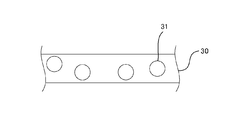
- FIG. 3 is a cross-sectional view schematically showing a part of an anisotropic conductive bonding film to which this technique is applied.
- the anisotropic conductive bonding film 30 is formed by dispersing the solder particles 31 in a thermosetting type insulating binder. Further, the anisotropic conductive film 30 may have the first film attached to the first surface and the second film attached to the second surface, if necessary.
- the anisotropic conductive bonding film is formed by forming an anisotropic conductive bonding material in the form of a film.
- the lower limit of the film thickness is 50% or more, preferably 80% or more, more preferably 90% or more of the average particle size of the solder particles. If the film thickness is too thin, the solder particles can be easily sandwiched between the electrodes, but there is a risk that the difficulty of forming the film will increase.
- the upper limit of the film thickness is 300% or less, preferably 200% or less, and more preferably 150% or less of the average particle size of the solder particles. If the film thickness is too thick, there is a risk that the bonding will be hindered.
- the film thickness can be measured using a known micrometer or digital thickness gauge (for example, Mitutoyo Co., Ltd .: MDE-25M, minimum display amount 0.0001 mm) capable of measuring 1 ⁇ m or less, preferably 0.1 ⁇ m or less. ..
- the film thickness may be obtained by measuring 10 or more points and averaging them.
- a contact-type thickness measuring instrument is not suitable, so it is preferable to use a laser displacement meter (for example, KEYENCE Co., Ltd., spectroscopic interference displacement type SI-T series, etc.). ..
- the film thickness is the thickness of the resin layer only, and does not include the particle size.
- thermosetting insulating binder examples include a thermal radical polymerization type resin composition containing a (meth) acrylate compound and a thermal radical polymerization initiator, and a thermal cation containing an epoxy compound and a thermal cationic polymerization initiator.
- examples thereof include a polymerizable resin composition, a thermal anion polymerizable resin composition containing an epoxy compound and a thermal anion polymerization initiator, and the like.
- the (meth) acrylic monomer means to include both an acrylic monomer and a methacrylic monomer.
- thermal anionic polymerization type resin composition containing a solid epoxy resin, a liquid epoxy resin, an epoxy resin curing agent, and a flux compound will be described as an example.
- the solid epoxy resin is not particularly limited as long as it is an epoxy resin that is solid at room temperature and has one or more epoxy groups in the molecule, and is, for example, a bisphenol A type epoxy resin, a biphenyl type epoxy resin, or the like. There may be. Thereby, the film shape can be maintained.
- the normal temperature is in the range of 20 ° C. ⁇ 15 ° C. (5 ° C. to 35 ° C.) defined by JIS Z8703.
- the liquid epoxy resin is not particularly limited as long as it is liquid at room temperature, and may be, for example, a bisphenol A type epoxy resin, a bisphenol F type epoxy resin, or a urethane-modified epoxy resin. Absent.
- the blending amount of the liquid epoxy resin is preferably 160 parts by mass or less, more preferably 100 parts by mass or less, and further preferably 70 parts by mass or less with respect to 100 parts by mass of the solid epoxy resin. When the amount of the liquid epoxy resin blended is large, it becomes difficult to maintain the film shape.
- the epoxy resin curing agent is not particularly limited as long as it is a thermosetting agent that starts curing by heat, and examples thereof include an anionic curing agent such as amine and imidazole, and a cationic curing agent such as a sulfonium salt. .. Further, the curing agent may be microencapsulated so as to obtain resistance to the solvent used for film formation.
- the curing agent may be a carboxylic acid or a blocked carboxylic acid in which the carboxyl group is blocked with an alkyl vinyl ether. That is, the curing agent may be a flux compound.
- the flux compound removes foreign matter and oxide film on the electrode surface, prevents oxidation of the electrode surface, and lowers the surface tension of molten solder.
- the flux compound for example, it is preferable to use a carboxylic acid such as levulinic acid, maleic acid, oxalic acid, malonic acid, succinic acid, glutaric acid, adipic acid, and sebacic acid.
- a carboxylic acid such as levulinic acid, maleic acid, oxalic acid, malonic acid, succinic acid, glutaric acid, adipic acid, and sebacic acid.
- the flux compound it is preferable to use a blocked carboxylic acid in which the carboxyl group is blocked with an alkyl vinyl ether. Thereby, it is possible to control the temperature at which the flux effect and the curing agent function are exhibited. Further, since the solubility in the resin is improved, it is possible to improve the mixing / coating unevenness at the time of forming a film. Further, the dissociation temperature at which the blocking is released is preferably equal to or higher than the melting point of the solder particles. As a result, a good solder connection can be obtained, and when the epoxy resin is blended, curing is started after the epoxy resin flows, so that a good solder bond can be obtained.
- solder particles may be randomly kneaded and dispersed in the anisotropic conductive bonding film, or may be arranged in a plan view. These may be used properly according to the purpose.
- the arrangement of the entire solder particles in the plan view of the anisotropic conductive bonding film may be a regular arrangement or a random arrangement. Examples of the mode of regular arrangement include lattice arrangements such as a square lattice, a hexagonal lattice, an orthorhombic lattice, and a rectangular lattice, and there are no particular restrictions.
- the solder particles exist without contacting each other in the plan view of the film, and the solder particles exist without overlapping each other in the film thickness direction. Further, it is preferable that 75% or more, preferably 95% or more of the total number of solder particles in the anisotropic conductive bonding film is non-contact with other solder particles and is independent. This is confirmed by observing 200 or more, preferably 1000 or more solder particles by arbitrarily extracting 5 or more areas of 1 mm 2 or more in a film plan view using a known metal microscope or optical microscope. Can be done. Further, when the solder particles are arranged in the anisotropic conductive bonding film in a plan view, the solder particles may be aligned at the same position in the film thickness direction.
- the solder particles may be arranged as agglomerates in which a plurality of the solder particles are agglomerated.
- the arrangement of the agglomerates in the plan view of the anisotropic bonded film may be a regular arrangement or a random arrangement as in the above-mentioned arrangement of the solder particles.
- the average particle size of the individual solder particles of the agglomerate can be measured in the same manner as the above-mentioned average particle size.
- the average particle size of the solder particles is preferably 1/3 or less, more preferably 1/4 or less, and further preferably 1/5 or less of the distance between the electrodes of the semiconductor element which is the adherend. is there. When the average particle size of the solder particles is larger than 1/3 of the distance between the electrodes of the semiconductor element, a short circuit is likely to occur.
- the lower limit of the average particle size of the solder particles is preferably 0.5 ⁇ m or more, more preferably 3 ⁇ m or more, and more preferably 5 ⁇ m or more. As a result, the coating thickness of the film can be made constant. If the average particle size of the solder particles is smaller than 0.5 ⁇ m, a good solder joint state with the electrode portion cannot be obtained, and the reliability tends to deteriorate.
- the upper limit of the average particle size of the solder particles is 30 ⁇ m or less, preferably 25 ⁇ m or less, and more preferably 20 ⁇ m or less.
- the upper limit of the average particle size of the solder particles can be 15 ⁇ m or less, preferably 12 ⁇ m or less, and more preferably 10 ⁇ m or less.
- the size of the agglomerates may be equal to the average particle size of the solder particles described above. In the case of agglomerates, the average particle size of the solder particles may be smaller than the above value. The size of each solder particle can be determined by observing with an electron microscope.
- the maximum diameter of the solder particles can be 200% or less of the average particle size, preferably 150% or less of the average particle size, and more preferably 120% or less of the average particle size.
- the solder particles can be sandwiched between the electrodes, and the electrodes can be joined by melting the solder particles.
- the thickness of the anisotropic conductive bonding material after pressurization may be the maximum diameter of the solder particles.
- the size of the agglomerate may be equal to the maximum diameter of the above-mentioned solder particles. In the case of agglomerates, the maximum diameter of the solder particles may be smaller than the above value.
- the size of each solder particle can be determined by observing with an electron microscope.
- the solder particles are, for example, Sn-Pb-based, Pb-Sn-Sb-based, Sn-Sb-based, Sn-Pb-Bi-based, Bi-Sn-based, Sn-Cu-based, as defined in JIS Z3282-1999. It can be appropriately selected from Sn-Pb-Cu type, Sn-In type, Sn-Ag type, Sn-Pb-Ag type, Pb-Ag type and the like according to the electrode material, connection conditions and the like.
- the lower limit of the melting point of the solder particles is preferably 110 ° C. or higher, more preferably 120 ° C. or higher, still more preferably 130 ° C. or higher.
- the upper limit of the melting point of the solder particles is preferably 180 ° C. or lower, more preferably 160 ° C. or lower, and further preferably 150 ° C. or lower.
- the solder particles may have a flux compound directly bonded to the surface for the purpose of activating the surface. By activating the surface, metal bonding with the electrode portion can be promoted.
- the lower limit of the mass ratio range of the blended amount of the solder particles is preferably 20 wt% or more, more preferably 30 wt% or more, still more preferably 40 wt% or more, and the upper limit of the mass ratio range of the blended amount of the solder particles is preferably. It is 80 wt% or less, more preferably 70 wt% or less, still more preferably 60 wt% or less.
- the lower limit of the volume ratio range of the blended amount of the solder particles is preferably 5 vol% or more, more preferably 10 vol% or more, still more preferably 15 vol% or more, and the upper limit of the volume ratio range of the blended amount of the solder particles is.
- the blending amount of the solder particles satisfies the above-mentioned mass ratio range or volume ratio range, excellent conductivity, heat dissipation, and adhesiveness can be obtained.
- the volume ratio may be used, and if the anisotropic conductive bonding material is produced (before the solder particles are present in the binder), the mass ratio may be used. .. The mass ratio can be converted into a volume ratio from the specific gravity of the compound, the compounding ratio, and the like.
- the blending amount of the solder particles is too small, excellent conductivity, heat dissipation, and adhesiveness cannot be obtained, and if the blending amount is too large, the anisotropy is likely to be impaired, and it becomes difficult to obtain the intended conduction performance.
- the anisotropic conductive bonding film may contain an inorganic filler, an organic filler, a metal filler, a coupling agent, a leveling agent, a stabilizer, a thixo agent, and the like.
- the particle size of the inorganic filler, the organic filler, and the metal filler is smaller than the average particle size of the solder particles from the viewpoint of connection stability.
- a nanofiller of 10 to 1000 nm, a microfiller of 1-10 ⁇ m, or the like is used. ..
- examples of the inorganic filler include silica, aluminum oxide, aluminum hydroxide, titanium oxide, aluminum hydroxide, calcium hydroxide, calcium carbonate, talc, zinc oxide, zeolite, etc.
- Silica is added for the purpose of improving moisture absorption reliability.
- titanium oxide may be added for the purpose of improving light reflection, or aluminum hydroxide, calcium hydroxide or the like may be added for the purpose of preventing corrosion by acid.
- Examples of the organic filler include acrylic resin, carbon, core-shell particles, etc. By adding the organic filler, effects such as blocking prevention and light scattering can be obtained.
- the metal filler examples include Ni, Cu, Ag, and Au, and alloys of these may be used.
- the Cu filler forms a complex with an acid, so that corrosion of electrodes and the like can be prevented.
- the metal filler may or may not contribute to conduction, and the blending amount of the metal filler may be adjusted so as not to cause a short circuit, including the solder particles.
- anisotropic conductive bonding film for example, an insulating binder and solder particles are mixed in a solvent, and this mixture is applied to a release-treated film by a bar coater so as to have a predetermined thickness. It can be obtained by drying and volatilizing the solvent. Further, the mixture may be applied on the peeling film by a bar coater and then pressed to a predetermined thickness. Further, in order to increase the dispersibility of the solder particles, it is preferable to apply a high share in a state containing a solvent. For example, a known batch type planetary stirrer can be used. It may be one that can be performed in a vacuum environment.
- the amount of residual solvent in the anisotropic conductive bonding film is preferably 2% or less, more preferably 1% or less.
- Example> anisotropic conductive bonding films having different curing temperatures were produced. Then, an LED mounting body was produced using the anisotropic conductive bonding film, and the forward voltage, die shear strength, and bonding state of the LED mounting body were evaluated.
- An anisotropic conductive bonding film was laminated on the substrate under the conditions of 60 ° C.-2 MPa-2sec, and an LED chip was mounted. After that, the LED chip was mounted by reflow.
- FIG. 4 is a graph showing the temperature profile of reflow. As shown in FIG. 4, the reflow gradually increased the temperature so that the peak temperature reached 180 ° C. in 240 sec.
- the temperature was raised from 20 ° C. to 120 ° C. in 60 seconds, and then in order to melt the solder particles and spread them wet, the temperature was raised from 120 ° C. to 140 ° C. in 60 seconds.
- the temperature was raised from 140 ° C. to 175 ° C. for 60 seconds, maintained at 175 ° C. to 180 ° C. for 60 seconds, and lowered from 180 ° C. to 160 ° C. for 60 seconds.
- Example 1 As shown in Table 1, solid epoxy resin (bisphenol F type epoxy resin, Mitsubishi Chemical Co., Ltd., JER4007P, softening point 108 ° C.), liquid epoxy resin (dicyclopentadiene skeleton epoxy resin, ADEKA Co., Ltd., EP4088L), Flux compound (glutaric acid (1,3-propanedicarboxylic acid), Tokyo Kasei Co., Ltd.), solder particles (Si-Bi, Mitsui Metal Co., Ltd., ST-7, melting point 139 ° C., average particle size (D50) 7 .1 ⁇ m) and an epoxy resin curing agent (imidazole-based curing agent, Shikoku Kasei Kogyo Co., Ltd., Curesol 2P4MHZ-PW) were blended in a predetermined mass portion to prepare an anisotropic conductive bonding film.
- bisphenol F type epoxy resin Mitsubishi Chemical Co., Ltd., JER4007P, softening point 108 ° C
- the main constituent epoxy resin dissolved in PMA (propylene glycol monomethyl ether acetate) and the liquid epoxy resin were mixed with the MEK (methyl ethyl ketone) dissolved product of the flux compound and the epoxy resin curing agent. After the solder particles were dispersed in this mixed solution, they were coated on a PET (polyethylene terephthalate) film so that the thickness after solvent drying was 10 ⁇ m with a gap coater to prepare an anisotropic conductive bonded film. Drying was carried out under the condition of 70 ° C.-5 min.
- Table 1 shows the measurement results of the forward voltage and die shear strength of the LED mount manufactured using the anisotropic conductive bonding film.
- the forward voltage was 3.1 V and the die share strength was 32 N / chip.
- FIG. 5 is a graph showing the measurement results of the differential scanning calorimetry of the anisotropic conductive bonded film of Example 1. From the graph shown in FIG. 5, it can be seen that the endothermic reaction of solder melting appears around 139 ° C. and the exothermic peak temperature of resin curing appears around 163 ° C.
- FIG. 6 is a photomicrograph when observing the solder bonding state on the substrate side after peeling off the LED chip of Example 1. It was confirmed that the solder was wet and spread on the LED chip side and the substrate side, and that the solder joint state was good. In addition, it was confirmed that there are a plurality of solder joints in one electrode.
- Example 2 As shown in Table 1, an anisotropic conductive bonded film was produced in the same manner as in Example 1 except that the solid epoxy resin (bisphenol F type epoxy resin, Mitsubishi Chemical Co., Ltd., JER4005P, softening point 87 ° C.) was replaced. did.
- the LED mount manufactured by using the anisotropic conductive bonding film had a forward voltage of 3.0 V and a die shear strength of 29 N / chip.
- Example 3 As shown in Table 1, an anisotropic conductive bonded film was produced in the same manner as in Example 1 except that the solid epoxy resin (bisphenol A type epoxy resin, Mitsubishi Chemical Co., Ltd., JER1004AF, softening point 97 ° C.) was replaced. did.
- the LED mount manufactured by using the anisotropic conductive bonding film had a forward voltage of 3.0 V and a die shear strength of 30 N / chip.
- an anisotropic conductive bonding film was produced in the same manner as in Example 1 except that the epoxy resin curing agent (ammonium salt-based acid generator, KINGINDUSTRIES Co., Ltd., CXC-1821) was replaced.
- the LED mounting body manufactured by using the anisotropic conductive bonding film had an open forward voltage and a die shear strength of 28 N / chip.
- Comparative Example 1 since the curing temperature of the anisotropic conductive bonding film was lower than the melting point of the solder particles, the binder of the anisotropic conductive bonding film was cured before the solder particles were melted. Therefore, the forward voltage could not be measured. Further, since the solder joint is not formed, the adhesion of the LED chip is weak and the die shear strength is low.
- the anisotropic conductive bonding film has a minimum melt viscosity reaching temperature lower than the melting point of the solder particles and a curing temperature higher than the melting point of the solder particles, and thus is anisotropic.
- the binder of the conductive bonding film melted and flowed, and the binder was cured with the solder particles sandwiched between the electrodes of the adherend. Therefore, a value close to the rated voltage of 3.1 V could be obtained.
- the die-share strength was also good.
Landscapes
- Chemical & Material Sciences (AREA)
- Organic Chemistry (AREA)
- Inorganic Chemistry (AREA)
- Physics & Mathematics (AREA)
- Dispersion Chemistry (AREA)
- Spectroscopy & Molecular Physics (AREA)
- Wire Bonding (AREA)
- Electric Connection Of Electric Components To Printed Circuits (AREA)
- Non-Insulated Conductors (AREA)
Priority Applications (2)
| Application Number | Priority Date | Filing Date | Title |
|---|---|---|---|
| KR1020227011856A KR102707134B1 (ko) | 2019-10-25 | 2020-10-14 | 접속체의 제조 방법, 이방성 도전 접합 재료, 및 접속체 |
| CN202080071245.7A CN114502685B (zh) | 2019-10-25 | 2020-10-14 | 连接体的制备方法、各向异性导电接合材料及连接体 |
Applications Claiming Priority (2)
| Application Number | Priority Date | Filing Date | Title |
|---|---|---|---|
| JP2019-194428 | 2019-10-25 | ||
| JP2019194428A JP7032367B2 (ja) | 2019-10-25 | 2019-10-25 | 接続体の製造方法、異方性導電接合材料、及び接続体 |
Publications (1)
| Publication Number | Publication Date |
|---|---|
| WO2021079812A1 true WO2021079812A1 (ja) | 2021-04-29 |
Family
ID=75620520
Family Applications (1)
| Application Number | Title | Priority Date | Filing Date |
|---|---|---|---|
| PCT/JP2020/038842 Ceased WO2021079812A1 (ja) | 2019-10-25 | 2020-10-14 | 接続体の製造方法、異方性導電接合材料、及び接続体 |
Country Status (5)
| Country | Link |
|---|---|
| JP (2) | JP7032367B2 (https=) |
| KR (1) | KR102707134B1 (https=) |
| CN (1) | CN114502685B (https=) |
| TW (1) | TWI870491B (https=) |
| WO (1) | WO2021079812A1 (https=) |
Families Citing this family (6)
| Publication number | Priority date | Publication date | Assignee | Title |
|---|---|---|---|---|
| JP2023092710A (ja) * | 2021-12-22 | 2023-07-04 | デクセリアルズ株式会社 | 接続構造体及び接続構造体の製造方法 |
| KR102677735B1 (ko) * | 2021-12-28 | 2024-06-24 | 주식회사 노피온 | 이방성 도전접착제 및 이의 조성물 |
| WO2023189416A1 (ja) | 2022-03-31 | 2023-10-05 | デクセリアルズ株式会社 | 導電フィルム、接続構造体及びその製造方法 |
| CN119895002A (zh) | 2022-09-30 | 2025-04-25 | 日东电工株式会社 | 接合片 |
| WO2025211339A1 (ja) * | 2024-04-03 | 2025-10-09 | 日東電工株式会社 | 導電組成物、導電シート、接続構造体、接続構造体の製造方法、積層体、及び、積層体の製造方法 |
| WO2026018836A1 (ja) * | 2024-07-16 | 2026-01-22 | デクセリアルズ株式会社 | 半田接続材料、接続構造体の製造方法、及び接続構造体 |
Citations (3)
| Publication number | Priority date | Publication date | Assignee | Title |
|---|---|---|---|---|
| JP2004260131A (ja) * | 2003-02-05 | 2004-09-16 | Japan Science & Technology Agency | 端子間の接続方法及び半導体装置の実装方法 |
| WO2015152164A1 (ja) * | 2014-03-31 | 2015-10-08 | デクセリアルズ株式会社 | 熱硬化性接着組成物、及び熱硬化性接着シート |
| WO2016104276A1 (ja) * | 2014-12-26 | 2016-06-30 | 積水化学工業株式会社 | 導電ペースト、接続構造体及び接続構造体の製造方法 |
Family Cites Families (10)
| Publication number | Priority date | Publication date | Assignee | Title |
|---|---|---|---|---|
| CN100409423C (zh) * | 2003-02-05 | 2008-08-06 | 千住金属工业株式会社 | 端子间的连接方法及半导体装置的安装方法 |
| JP5032938B2 (ja) | 2007-10-24 | 2012-09-26 | パナソニック株式会社 | 熱硬化性樹脂組成物及びその製造方法 |
| JP2009147231A (ja) | 2007-12-17 | 2009-07-02 | Hitachi Chem Co Ltd | 実装方法、半導体チップ、及び半導体ウエハ |
| JP2010040893A (ja) * | 2008-08-07 | 2010-02-18 | Sumitomo Bakelite Co Ltd | 端子間の接続方法、それを用いた半導体装置の製造方法、および導電性粒子の凝集方法 |
| CN102171306B (zh) | 2008-09-30 | 2014-08-13 | 迪睿合电子材料有限公司 | 各向异性导电粘结剂及使用该粘结剂的连接结构体的制备方法 |
| JP6114627B2 (ja) | 2012-05-18 | 2017-04-12 | 積水化学工業株式会社 | 導電材料、接続構造体及び接続構造体の製造方法 |
| JP6114557B2 (ja) | 2013-01-10 | 2017-04-12 | 積水化学工業株式会社 | 導電材料及び接続構造体の製造方法 |
| WO2015056754A1 (ja) | 2013-10-17 | 2015-04-23 | デクセリアルズ株式会社 | 異方性導電接着剤及び接続構造体 |
| JP6557591B2 (ja) | 2014-12-26 | 2019-08-07 | 積水化学工業株式会社 | 導電フィルム、接続構造体及び接続構造体の製造方法 |
| KR101820214B1 (ko) * | 2015-11-27 | 2018-01-18 | 이경섭 | 미세피치용 이방성 도전 접착제 제조방법 및 이 방법에 의해 제조된 미세피치용 이방성 도전 접착제 |
-
2019
- 2019-10-25 JP JP2019194428A patent/JP7032367B2/ja active Active
-
2020
- 2020-10-14 WO PCT/JP2020/038842 patent/WO2021079812A1/ja not_active Ceased
- 2020-10-14 CN CN202080071245.7A patent/CN114502685B/zh active Active
- 2020-10-14 KR KR1020227011856A patent/KR102707134B1/ko active Active
- 2020-10-23 TW TW109136910A patent/TWI870491B/zh active
-
2022
- 2022-02-24 JP JP2022026731A patent/JP7432633B2/ja active Active
Patent Citations (3)
| Publication number | Priority date | Publication date | Assignee | Title |
|---|---|---|---|---|
| JP2004260131A (ja) * | 2003-02-05 | 2004-09-16 | Japan Science & Technology Agency | 端子間の接続方法及び半導体装置の実装方法 |
| WO2015152164A1 (ja) * | 2014-03-31 | 2015-10-08 | デクセリアルズ株式会社 | 熱硬化性接着組成物、及び熱硬化性接着シート |
| WO2016104276A1 (ja) * | 2014-12-26 | 2016-06-30 | 積水化学工業株式会社 | 導電ペースト、接続構造体及び接続構造体の製造方法 |
Also Published As
| Publication number | Publication date |
|---|---|
| JP7432633B2 (ja) | 2024-02-16 |
| CN114502685A (zh) | 2022-05-13 |
| TW202122535A (zh) | 2021-06-16 |
| JP2022060494A (ja) | 2022-04-14 |
| JP2021068842A (ja) | 2021-04-30 |
| JP7032367B2 (ja) | 2022-03-08 |
| TWI870491B (zh) | 2025-01-21 |
| CN114502685B (zh) | 2024-04-12 |
| KR102707134B1 (ko) | 2024-09-13 |
| KR20220062055A (ko) | 2022-05-13 |
Similar Documents
| Publication | Publication Date | Title |
|---|---|---|
| JP6898413B2 (ja) | 接続体の製造方法、異方性接合フィルム、接続体 | |
| JP7032367B2 (ja) | 接続体の製造方法、異方性導電接合材料、及び接続体 | |
| TWI798321B (zh) | 焊料粒子、導電材料、焊料粒子之保管方法、導電材料之保管方法、導電材料之製造方法、連接構造體及連接構造體之製造方法 | |
| JP6949258B2 (ja) | 接続体の製造方法及び接続体 | |
| TWI902241B (zh) | 連接體之製造方法 | |
| JP2022074048A (ja) | 導電性接着剤、異方性導電フィルム、接続構造体、及び接続構造体の製造方法 | |
| JP2022000914A (ja) | 接続体の製造方法及び接続体 | |
| WO2021200553A1 (ja) | 半導体用接着剤、並びに、半導体装置及びその製造方法 | |
| JP6430148B2 (ja) | 接着剤及び接続構造体 | |
| WO2023162666A1 (ja) | 接続構造体の製造方法、フィルム構造体、及びフィルム構造体の製造方法 | |
| TWI916754B (zh) | 異向性接合材料、異向性接合膜、及連接體 | |
| TW202223031A (zh) | 導電性接著劑、異向性導電膜、連接結構體、及連接結構體之製造方法 | |
| JP7790938B2 (ja) | 接続構造体の製造方法及び接続構造体 | |
| JP2023092710A (ja) | 接続構造体及び接続構造体の製造方法 | |
| JP2023079632A (ja) | 接続構造体、及び接続構造体の製造方法 | |
| WO2026018836A1 (ja) | 半田接続材料、接続構造体の製造方法、及び接続構造体 | |
| JP2026013403A (ja) | 半田接続材料、接続構造体の製造方法、及び接続構造体 |
Legal Events
| Date | Code | Title | Description |
|---|---|---|---|
| 121 | Ep: the epo has been informed by wipo that ep was designated in this application |
Ref document number: 20878877 Country of ref document: EP Kind code of ref document: A1 |
|
| ENP | Entry into the national phase |
Ref document number: 20227011856 Country of ref document: KR Kind code of ref document: A |
|
| NENP | Non-entry into the national phase |
Ref country code: DE |
|
| 122 | Ep: pct application non-entry in european phase |
Ref document number: 20878877 Country of ref document: EP Kind code of ref document: A1 |