WO2021079812A1 - Method for producing connected structure, anisotropic electroconductive bonding material, and connected structure - Google Patents
Method for producing connected structure, anisotropic electroconductive bonding material, and connected structure Download PDFInfo
- Publication number
- WO2021079812A1 WO2021079812A1 PCT/JP2020/038842 JP2020038842W WO2021079812A1 WO 2021079812 A1 WO2021079812 A1 WO 2021079812A1 JP 2020038842 W JP2020038842 W JP 2020038842W WO 2021079812 A1 WO2021079812 A1 WO 2021079812A1
- Authority
- WO
- WIPO (PCT)
- Prior art keywords
- solder particles
- anisotropic conductive
- conductive bonding
- electronic component
- temperature
- Prior art date
Links
Images


Classifications
-
- C—CHEMISTRY; METALLURGY
- C09—DYES; PAINTS; POLISHES; NATURAL RESINS; ADHESIVES; COMPOSITIONS NOT OTHERWISE PROVIDED FOR; APPLICATIONS OF MATERIALS NOT OTHERWISE PROVIDED FOR
- C09J—ADHESIVES; NON-MECHANICAL ASPECTS OF ADHESIVE PROCESSES IN GENERAL; ADHESIVE PROCESSES NOT PROVIDED FOR ELSEWHERE; USE OF MATERIALS AS ADHESIVES
- C09J163/00—Adhesives based on epoxy resins; Adhesives based on derivatives of epoxy resins
-
- C—CHEMISTRY; METALLURGY
- C09—DYES; PAINTS; POLISHES; NATURAL RESINS; ADHESIVES; COMPOSITIONS NOT OTHERWISE PROVIDED FOR; APPLICATIONS OF MATERIALS NOT OTHERWISE PROVIDED FOR
- C09J—ADHESIVES; NON-MECHANICAL ASPECTS OF ADHESIVE PROCESSES IN GENERAL; ADHESIVE PROCESSES NOT PROVIDED FOR ELSEWHERE; USE OF MATERIALS AS ADHESIVES
- C09J11/00—Features of adhesives not provided for in group C09J9/00, e.g. additives
- C09J11/02—Non-macromolecular additives
- C09J11/04—Non-macromolecular additives inorganic
-
- C—CHEMISTRY; METALLURGY
- C09—DYES; PAINTS; POLISHES; NATURAL RESINS; ADHESIVES; COMPOSITIONS NOT OTHERWISE PROVIDED FOR; APPLICATIONS OF MATERIALS NOT OTHERWISE PROVIDED FOR
- C09J—ADHESIVES; NON-MECHANICAL ASPECTS OF ADHESIVE PROCESSES IN GENERAL; ADHESIVE PROCESSES NOT PROVIDED FOR ELSEWHERE; USE OF MATERIALS AS ADHESIVES
- C09J11/00—Features of adhesives not provided for in group C09J9/00, e.g. additives
- C09J11/02—Non-macromolecular additives
- C09J11/06—Non-macromolecular additives organic
-
- C—CHEMISTRY; METALLURGY
- C09—DYES; PAINTS; POLISHES; NATURAL RESINS; ADHESIVES; COMPOSITIONS NOT OTHERWISE PROVIDED FOR; APPLICATIONS OF MATERIALS NOT OTHERWISE PROVIDED FOR
- C09J—ADHESIVES; NON-MECHANICAL ASPECTS OF ADHESIVE PROCESSES IN GENERAL; ADHESIVE PROCESSES NOT PROVIDED FOR ELSEWHERE; USE OF MATERIALS AS ADHESIVES
- C09J7/00—Adhesives in the form of films or foils
- C09J7/30—Adhesives in the form of films or foils characterised by the adhesive composition
- C09J7/35—Heat-activated
-
- C—CHEMISTRY; METALLURGY
- C09—DYES; PAINTS; POLISHES; NATURAL RESINS; ADHESIVES; COMPOSITIONS NOT OTHERWISE PROVIDED FOR; APPLICATIONS OF MATERIALS NOT OTHERWISE PROVIDED FOR
- C09J—ADHESIVES; NON-MECHANICAL ASPECTS OF ADHESIVE PROCESSES IN GENERAL; ADHESIVE PROCESSES NOT PROVIDED FOR ELSEWHERE; USE OF MATERIALS AS ADHESIVES
- C09J9/00—Adhesives characterised by their physical nature or the effects produced, e.g. glue sticks
- C09J9/02—Electrically-conducting adhesives
-
- H—ELECTRICITY
- H01—ELECTRIC ELEMENTS
- H01B—CABLES; CONDUCTORS; INSULATORS; SELECTION OF MATERIALS FOR THEIR CONDUCTIVE, INSULATING OR DIELECTRIC PROPERTIES
- H01B1/00—Conductors or conductive bodies characterised by the conductive materials; Selection of materials as conductors
- H01B1/20—Conductive material dispersed in non-conductive organic material
- H01B1/22—Conductive material dispersed in non-conductive organic material the conductive material comprising metals or alloys
-
- H—ELECTRICITY
- H01—ELECTRIC ELEMENTS
- H01R—ELECTRICALLY-CONDUCTIVE CONNECTIONS; STRUCTURAL ASSOCIATIONS OF A PLURALITY OF MUTUALLY-INSULATED ELECTRICAL CONNECTING ELEMENTS; COUPLING DEVICES; CURRENT COLLECTORS
- H01R11/00—Individual connecting elements providing two or more spaced connecting locations for conductive members which are, or may be, thereby interconnected, e.g. end pieces for wires or cables supported by the wire or cable and having means for facilitating electrical connection to some other wire, terminal, or conductive member, blocks of binding posts
- H01R11/01—Individual connecting elements providing two or more spaced connecting locations for conductive members which are, or may be, thereby interconnected, e.g. end pieces for wires or cables supported by the wire or cable and having means for facilitating electrical connection to some other wire, terminal, or conductive member, blocks of binding posts characterised by the form or arrangement of the conductive interconnection between the connecting locations
Definitions
- the present invention relates to a method for manufacturing a connector for mounting a semiconductor chip (element), an anisotropic conductive bonding material, and a connector.
- Flip chip mounting is one of the methods for mounting semiconductor chips (elements). Flip chip mounting can reduce the mounting area as compared with wire bonding, and can mount small and thin semiconductor chips.
- Patent Document 1 describes that a plurality of parts are collectively mounted on a wiring board or the like by reflow using a solder paste containing solder particles, a thermosetting resin binder, and a flux component.
- solder paste of Patent Document 1 contains a large amount of solder particles in order to melt and integrate the solder particles, and it is difficult to join electronic components provided with fine pitch electrodes.
- This technology has been proposed in view of such conventional circumstances, and is a method for manufacturing a connector capable of bonding electronic components provided with fine pitch electrodes, an anisotropic conductive bonding material, and a connector. I will provide a.
- the present inventor has found that the above object can be achieved by using an anisotropic conductive bonding material that exhibits conductivity only in the direction in which the conductive particles are sandwiched, and completes the present invention. I arrived.
- the solder particles are dispersed in a heat-curable insulating binder, and the minimum melt viscosity reaching temperature lower than the melting point of the solder particles and the melting point of the solder particles are obtained.
- An anisotropic conductive bonding material having a higher curing temperature is interposed between the electrodes of the first electronic component and the electrodes of the second electronic component, and the electrodes of the first electronic component and the second electronic component are interposed.
- the electrodes of the electronic parts of the above are joined with no load using a reflow furnace, and the peak temperature of the reflow furnace is 10 degrees or more higher than the curing temperature of the anisotropic conductive bonding material.
- the solder particles are dispersed in a thermosetting insulating binder, and the minimum melt viscosity reaching temperature lower than the melting point of the solder particles and the solder particles have a minimum melt viscosity reaching temperature. It has a curing temperature higher than its melting point.
- the electrode of the first electronic component and the electrode of the second electronic component are bonded by using the above-mentioned anisotropic conductive bonding material.
- the insulating binder is melted by heating and the binder is cured in a state where the solder particles are sandwiched between the electrodes, it is possible to join electronic components having fine pitch electrodes.
- FIG. 1 is a cross-sectional view schematically showing a part of the joining process.
- FIG. 2 is a cross-sectional view showing a configuration example of the LED mounting body.
- FIG. 3 is a cross-sectional view schematically showing a part of an anisotropic conductive bonding film to which the present technology is applied.
- FIG. 4 is a graph showing the temperature profile of reflow.
- FIG. 5 is a graph showing the measurement results of differential scanning calorimetry (DSC) of the anisotropic conductive bonded film of Example 1.
- FIG. 6 is a photomicrograph when observing the solder bonding state on the substrate side after peeling off the LED chip of Example 1.
- the solder particles are dispersed in a thermosetting insulating binder, and the minimum melt viscosity reaching temperature lower than the melting point of the solder particles and higher than the melting point of the solder particles are higher.
- An anisotropic conductive bonding material having a curing temperature is interposed between the electrodes of the first electronic component and the electrodes of the second electronic component, and the electrodes of the first electronic component and the electrodes of the second electronic component are interposed. Is bonded using a reflow furnace with no load, and the peak temperature of the reflow furnace is 10 degrees or more higher than the curing temperature of the anisotropic conductive bonding material.
- the temperature at which the minimum melt viscosity of the anisotropic conductive bonding material is reached is, for example, a measurement pressure of 5 g, a temperature range of 30 to 200 ° C., and a temperature rise rate of 10 ° C. using a rotary leometer (manufactured by TA instrument).
- the curing temperature of the anisotropic conductive bonding material is the heat generated by measuring 5 mg or more of the sample with an aluminum pan by differential thermal analysis (DSC) under the conditions of a temperature range of 30 to 250 ° C. and a heating rate of 10 ° C./min. It is the peak temperature.
- the connecting body is one in which two materials or members are electrically connected.
- joining is the joining of two materials or members. No load means that there is no mechanical pressurization.
- the first electronic component may be one provided with wiring (conducting material) such as LED (Light Emitting Diode), driver IC (Integrated Circuit), flexible substrate (FPC: Flexible Printed Circuits, resin molded component, etc.). Of these, chips such as LEDs and driver ICs (for example, semiconductor elements) are preferable.
- a terminal corresponding to at least a part of the terminal of the first electronic component is provided.
- a substrate so-called printed wiring board: PWB
- PWB printed wiring board
- a rigid substrate or glass may be used. Examples include substrates such as substrates, flexible printed circuits (FPCs), ceramic substrates, and plastic substrates.
- the same components may be laminated and connected. The number of these layers hinders the connection. If not, there is no particular limitation. The same applies to the case where a large number of dissimilar parts are laminated.
- the electrodes (electrode arrangement, electrode group) provided on the first electronic component and the second electronic component are opposed to each other. It is provided so as to be anisotropically connected, and electrodes (electrode arrangement, electrode group) may be provided so that a plurality of first electronic components are mounted on one second electronic component. It is desirable that the above-mentioned electronic components have heat resistance in the reflow process.
- the connector in this embodiment is connected by solder particles, which are widely used in BGA (Ball grid array) and the like, and has high connection reliability. Therefore, sensor devices, in-vehicle devices, and IoT (Internet of Things) ) It can be applied to many applications such as equipment.
- the anisotropic conductive bonding material may be either a film-shaped anisotropic conductive bonding film or a paste-shaped anisotropic conductive bonding paste. Further, the anisotropic conductive bonding paste may be formed into a film at the time of connection, or may be formed into a form similar to a film by mounting a component.
- anisotropic conductive bonding paste it suffices if a predetermined amount can be uniformly applied onto the substrate. For example, application methods such as dispensing, stamping, and screen printing can be used, and the paste may be dried if necessary. Good.
- an anisotropic conductive bonding film it is particularly preferable because not only the amount of the anisotropic conductive bonding material can be made uniform depending on the film thickness, but also the tact can be shortened because it can be laminated on the substrate at once. .. In addition, since it is easy to handle by forming it into a film in advance, it can be expected that work efficiency will be improved.
- solder particles are dispersed in a heat-curable insulating binder, and a minimum melt viscosity reaching temperature lower than the melting point of the solder particles and a curing temperature higher than the melting point of the solder particles are set.
- a plurality of parts may be mounted at once.
- the step of providing the anisotropic conductive bonding material may be a step of forming a film on the substrate before connecting the anisotropic conductive bonding paste, as used in the conventional anisotropic conductive film. It may be a temporary sticking step of sticking an anisotropic conductive bonding film on a substrate at a low temperature and a low pressure, or a laminating step of laminating an anisotropic conductive bonding film on a substrate.
- the anisotropic conductive bonding film can be provided on the substrate under known usage conditions. In this case, only minimal changes such as installation and change of tools from the conventional device are required, which is economically advantageous.
- the anisotropic conductive bonding film is laminated on the substrate using a pressure type laminator.
- the laminating step may be a vacuum pressurization type.
- the width of the film is restricted by the tool width, but in the laminating process, the heating-pressing tool is not used, so it is relatively wide. It can be expected that the width can be mounted all at once.
- one anisotropic conductive bonding film may be laminated on one substrate.
- the vertical movement of the heat-bonding tool and the transfer of the anisotropic conductive bonding film are not performed a plurality of times, so that the time required for the step of providing the anisotropic conductive bonding material can be shortened.
- the thickness of the anisotropic bonding material between the electrode of the LED element and the electrode of the substrate is approximated to the average particle size of the solder particles.
- the lower limit of the thickness of the anisotropic bonding material is 50% or more, preferably 80% or more, more preferably 90% or more of the average particle size of the solder particles. If the thickness of the anisotropic bonding material is too thin, the solder particles can be easily sandwiched between the electrodes, but there is a risk that the difficulty of forming the solder particles into a film will increase.
- the upper limit of the thickness of the anisotropic bonding material is 300% or less, preferably 200% or less, and more preferably 150% or less of the average particle size of the solder particles. If the thickness of the anisotropic bonding material is too thick, the bonding may be hindered.
- the average particle size obtained from the observed image or the image-type particle size distribution measuring device can be the average value of the maximum lengths of the particles.
- the particle size (D50) and the arithmetic mean diameter (volume basis) at which the cumulative frequency in the particle size distribution simply obtained by the laser diffraction / scattering method is 50% are 50%.
- the manufacturer value such as (preferably) can be used.
- each LED element has, for example, a first conductive type electrode and a second conductive type electrode on one side, and is arranged on an electrode of a substrate 30 corresponding to the first conductive type electrode and the second conductive type electrode.
- the thickness of the anisotropic bonding material between the electrode of the LED element and the electrode of the substrate was made to be close to the average particle size of the solder particles.
- the thickness of the anisotropic bonding material may be approximated to the average particle size of the solder particles by pressurization.
- the thickness of the anisotropic bonding material between the electrode of the LED element and the electrode of the substrate is applied by pressurizing from the side of the first electronic component mounted on the second electronic component. Is approximated to the average particle size of the solder particles.
- the thickness of the anisotropic bonding material is too large, it may interfere with pressurization, so it can be said that it is preferable to set the thickness to the above-mentioned upper limit.
- Approximate to the average particle size means that the maximum diameter of the solder particles is theoretically the thickness of the anisotropic connecting material after this pressurization step, so the thickness of the anisotropic connecting material is the maximum diameter of the solder particles. It may be considered to be equivalent, and if thickness variation is taken into consideration, it may be 130% or less, preferably 120% or less of the maximum diameter of the solder particles.
- the lower limit of the pressure in the pressurizing step is preferably 0.2 MPa or more, more preferably 0.4 MPa or more, and the upper limit of the pressure in the pressurizing step may be 2.0 MPa or less, preferably 1. It is 0 MPa or less, more preferably 0.8 MPa or less. Since the upper limit and the lower limit may vary depending on the specifications of the device, the upper limit and the lower limit are not limited to the above numerical range as long as the purpose of pushing the resin to the solder particle size can be achieved.
- FIG. 1 is a cross-sectional view schematically showing a part of the joining process.
- the electrodes 11 and 12 of the LED element 10 and the electrodes 21 and 21 of the substrate 20 are heat-bonded with no load.
- Examples of the method of heat-joining with no load without mechanical pressurization include atmospheric pressure reflow, vacuum reflow, atmospheric pressure oven, autoclave (pressurized oven), etc. Among these, the method is included in the joint. It is preferable to use a vacuum reflow, an autoclave, or the like that can eliminate air bubbles. Since no load is applied, unnecessary resin flow is not generated as compared with the anisotropic conductive connection using a general heating and pressurizing tool, so that the effect of suppressing the entrainment of air bubbles can be expected.
- the peak temperature in the reflow furnace is required to be 10 ° C. or higher than the curing temperature of the anisotropic conductive bonding material, preferably 150 ° C. or higher and 250 ° C. or lower, more preferably 160 ° C. or higher and 230 ° C. or lower, and further preferably 170 ° C. or higher.
- Main heating is performed at ° C. or higher and 210 ° C. or lower.
- solder bonding means connecting the electrodes of opposing electronic components by melting the solder.
- thermosetting resin In the reflow furnace, the thermosetting resin is melted by heating, the solder particles 31 are sandwiched between the electrodes by the weight of the LED element 10, the solder particles 31 are melted by the main heating which is equal to or higher than the solder melting point, and the solder wets and spreads on the electrodes. By cooling, the electrodes of the LED element 10 and the electrodes of the substrate 20 are joined.
- the reflow may include a step of maintaining a constant temperature (keeping step) in addition to a step of raising the temperature and a step of lowering the temperature. There may be a peak step at the highest temperature, and the step may be included in the middle of raising or lowering the temperature.
- the temperature raising step may be two steps: a step of melting the binder (example: up to 120 ° C. in FIG. 4) and a step of melting and spreading the solder particles (example: 120 to 175 ° C. in FIG. 4). .. Therefore, the heating rate may be 10 to 120 ° C./min or 20 to 100 ° C./min as an example.
- the maintenance time of the keeping step (eg, 175 to 180 ° C. in FIG. 4) is also a step of curing the binder. This temperature is, for example, a temperature of 160 to 230 ° C., and may have a difference of about 5 to 10 ° C., and may be the same as the peak temperature.
- the life performance of the binder will deteriorate and handling will be hindered. Therefore, it is 0.5 min or more, preferably 0.75 min or more. If it is too long, the production efficiency will deteriorate. Therefore, it is 5 min or less, preferably 3 min or less. Is.
- the temperature lowering rate should be high because it can be taken out quickly, and it is desirable that the joint state is not rapidly cooled to improve the quality of the joint, so it is better to be low.
- the rate may be the same as that in the temperature raising step, and is preferably 10 to 30 ° C./min.
- the temperature lowering rate can be adjusted according to the combination of the objects to be joined and the conditions of the binder used. It also affects the take-out temperature and its environment.
- the solder particles and the film thickness are approximated before the reflow process, and the solder particles and the electrodes are brought into contact with each other, so that the bonding can be performed more easily.
- thermosetting behavior of the anisotropic conductive bonding film resin melting during non-load connection, solder particles sandwiched between electrodes, and solder melting / Resin curing can be optimized.
- the thermosetting behavior of the anisotropic conductive bonded film can be known by DSC measurement or viscosity measurement with a rheometer.
- FIG. 2 is a cross-sectional view showing a configuration example of the LED mounting body.
- the LED element 10 and the substrate 20 are connected by using an anisotropic conductive bonding film in which solder particles 31 are dispersed in a thermosetting insulating binder. That is, the LED mount has an LED element 10, a substrate 20, and solder particles 31, and is anisotropic conductive formed by connecting the electrodes 11 and 12 of the LED element 10 and the electrodes 21 and 22 of the substrate 20.
- the bonding film 32 is provided, and the electrodes 11 and 12 of the LED element 10 and the electrodes 21 and 22 of the substrate 20 are bonded by a solder bonding portion 33, and a solid resin is formed between the LED element 10 and the substrate 20. It is filled.
- the LED element 10 includes a first conductive type electrode 11 and a second conductive type electrode 12, and when a voltage is applied between the first conductive type electrode 11 and the second conductive type electrode 12, a carrier is applied to the active layer in the element. Are concentrated and recombined to generate light.
- the distance between the space between the first conductive type electrode 11 and the second conductive type electrode 12 depends on the element size, for example, 100 ⁇ m or more and 200 ⁇ m or less, 100 ⁇ m or more and 50 ⁇ m or less, and 20 ⁇ m or more and 50 ⁇ m or less. is there.
- the LED element 10 is not particularly limited, but for example, a blue LED having a peak wavelength of 400 nm-500 nm or the like can be preferably used.
- the substrate 20 has a first electrode 21 and a second electrode 22 at positions corresponding to the first conductive type electrode 11 and the second conductive type electrode 12 of the LED element 10 on the base material, respectively.
- the substrate 20 include a printed wiring board, a glass substrate, a flexible substrate, a ceramic substrate, a plastic substrate, and the like.
- the electrode height of the printed wiring board is, for example, 10 ⁇ m or more and 40 ⁇ m or less
- the electrode height of the glass substrate is, for example, 3 ⁇ m or less
- the electrode height of the flexible substrate is, for example, 5 ⁇ m or more and 20 ⁇ m or less.
- the anisotropic conductive bonding film 32 is obtained by forming the anisotropic conductive bonding material into a film after the bonding step, and the electrodes 11 and 12 of the LED element 10 and the electrodes 21 and 22 of the substrate 20 are soldered to the solder bonding portion 33. Along with metal bonding, an anisotropic conductive bonding material is filled between the LED element 10 and the substrate 20.
- the terminals (electrodes 11 and 12) of the LED element 10 and the terminals (electrodes 21 and 22) of the substrate 20 are metal-bonded by the solder joint 33, and the LED element.
- a solid resin is filled between the 20 and the substrate 30. As a result, it is possible to prevent moisture or the like from entering between the LED element 10 and the substrate 20.
- Anisotropic conductive bonding material In the anisotropic conductive bonding material of the present embodiment, the solder particles are dispersed in a thermosetting insulating binder, and the minimum melt viscosity reaching temperature lower than the melting point of the solder particles and the melting point of the solder particles are obtained. It has a higher curing temperature than.
- the curing temperature is the exothermic peak temperature measured under the condition of a heating rate of 10 ° C./min as described above.
- the curing temperature of the anisotropic conductive bonding material is preferably 150 ° C. or higher and 200 ° C. or lower.
- the minimum melt viscosity of the anisotropic conductive bonding material may be less than 100 Pa ⁇ s, preferably 50 Pa ⁇ s or less, more preferably 30 Pa ⁇ s or less, and further preferably 10 Pa ⁇ s or less. If the minimum melt viscosity is too high, the resin will not melt under no load in the reflow process, which may hinder the sandwiching between the solder particles and the electrodes. In this technology, since no load is applied when the binder resin is heat-cured, it is set lower than the minimum melt viscosity of the binder resin on the assumption that a load is applied (pressed with a tool like a general anisotropic connection). There is a need to.
- the temperature at which the minimum melt viscosity of the anisotropic conductive bonding material is reached is preferably ⁇ 10 ° C. to ⁇ 60 ° C., which is the melting temperature of the solder particles, more preferably ⁇ 10 ° C. to ⁇ 50 ° C., which is the melting temperature of the solder particles.
- the melting temperature of the solder particles is preferably ⁇ 10 ° C. to ⁇ 40 ° C.
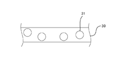
- FIG. 3 is a cross-sectional view schematically showing a part of an anisotropic conductive bonding film to which this technique is applied.
- the anisotropic conductive bonding film 30 is formed by dispersing the solder particles 31 in a thermosetting type insulating binder. Further, the anisotropic conductive film 30 may have the first film attached to the first surface and the second film attached to the second surface, if necessary.
- the anisotropic conductive bonding film is formed by forming an anisotropic conductive bonding material in the form of a film.
- the lower limit of the film thickness is 50% or more, preferably 80% or more, more preferably 90% or more of the average particle size of the solder particles. If the film thickness is too thin, the solder particles can be easily sandwiched between the electrodes, but there is a risk that the difficulty of forming the film will increase.
- the upper limit of the film thickness is 300% or less, preferably 200% or less, and more preferably 150% or less of the average particle size of the solder particles. If the film thickness is too thick, there is a risk that the bonding will be hindered.
- the film thickness can be measured using a known micrometer or digital thickness gauge (for example, Mitutoyo Co., Ltd .: MDE-25M, minimum display amount 0.0001 mm) capable of measuring 1 ⁇ m or less, preferably 0.1 ⁇ m or less. ..
- the film thickness may be obtained by measuring 10 or more points and averaging them.
- a contact-type thickness measuring instrument is not suitable, so it is preferable to use a laser displacement meter (for example, KEYENCE Co., Ltd., spectroscopic interference displacement type SI-T series, etc.). ..
- the film thickness is the thickness of the resin layer only, and does not include the particle size.
- thermosetting insulating binder examples include a thermal radical polymerization type resin composition containing a (meth) acrylate compound and a thermal radical polymerization initiator, and a thermal cation containing an epoxy compound and a thermal cationic polymerization initiator.
- examples thereof include a polymerizable resin composition, a thermal anion polymerizable resin composition containing an epoxy compound and a thermal anion polymerization initiator, and the like.
- the (meth) acrylic monomer means to include both an acrylic monomer and a methacrylic monomer.
- thermal anionic polymerization type resin composition containing a solid epoxy resin, a liquid epoxy resin, an epoxy resin curing agent, and a flux compound will be described as an example.
- the solid epoxy resin is not particularly limited as long as it is an epoxy resin that is solid at room temperature and has one or more epoxy groups in the molecule, and is, for example, a bisphenol A type epoxy resin, a biphenyl type epoxy resin, or the like. There may be. Thereby, the film shape can be maintained.
- the normal temperature is in the range of 20 ° C. ⁇ 15 ° C. (5 ° C. to 35 ° C.) defined by JIS Z8703.
- the liquid epoxy resin is not particularly limited as long as it is liquid at room temperature, and may be, for example, a bisphenol A type epoxy resin, a bisphenol F type epoxy resin, or a urethane-modified epoxy resin. Absent.
- the blending amount of the liquid epoxy resin is preferably 160 parts by mass or less, more preferably 100 parts by mass or less, and further preferably 70 parts by mass or less with respect to 100 parts by mass of the solid epoxy resin. When the amount of the liquid epoxy resin blended is large, it becomes difficult to maintain the film shape.
- the epoxy resin curing agent is not particularly limited as long as it is a thermosetting agent that starts curing by heat, and examples thereof include an anionic curing agent such as amine and imidazole, and a cationic curing agent such as a sulfonium salt. .. Further, the curing agent may be microencapsulated so as to obtain resistance to the solvent used for film formation.
- the curing agent may be a carboxylic acid or a blocked carboxylic acid in which the carboxyl group is blocked with an alkyl vinyl ether. That is, the curing agent may be a flux compound.
- the flux compound removes foreign matter and oxide film on the electrode surface, prevents oxidation of the electrode surface, and lowers the surface tension of molten solder.
- the flux compound for example, it is preferable to use a carboxylic acid such as levulinic acid, maleic acid, oxalic acid, malonic acid, succinic acid, glutaric acid, adipic acid, and sebacic acid.
- a carboxylic acid such as levulinic acid, maleic acid, oxalic acid, malonic acid, succinic acid, glutaric acid, adipic acid, and sebacic acid.
- the flux compound it is preferable to use a blocked carboxylic acid in which the carboxyl group is blocked with an alkyl vinyl ether. Thereby, it is possible to control the temperature at which the flux effect and the curing agent function are exhibited. Further, since the solubility in the resin is improved, it is possible to improve the mixing / coating unevenness at the time of forming a film. Further, the dissociation temperature at which the blocking is released is preferably equal to or higher than the melting point of the solder particles. As a result, a good solder connection can be obtained, and when the epoxy resin is blended, curing is started after the epoxy resin flows, so that a good solder bond can be obtained.
- solder particles may be randomly kneaded and dispersed in the anisotropic conductive bonding film, or may be arranged in a plan view. These may be used properly according to the purpose.
- the arrangement of the entire solder particles in the plan view of the anisotropic conductive bonding film may be a regular arrangement or a random arrangement. Examples of the mode of regular arrangement include lattice arrangements such as a square lattice, a hexagonal lattice, an orthorhombic lattice, and a rectangular lattice, and there are no particular restrictions.
- the solder particles exist without contacting each other in the plan view of the film, and the solder particles exist without overlapping each other in the film thickness direction. Further, it is preferable that 75% or more, preferably 95% or more of the total number of solder particles in the anisotropic conductive bonding film is non-contact with other solder particles and is independent. This is confirmed by observing 200 or more, preferably 1000 or more solder particles by arbitrarily extracting 5 or more areas of 1 mm 2 or more in a film plan view using a known metal microscope or optical microscope. Can be done. Further, when the solder particles are arranged in the anisotropic conductive bonding film in a plan view, the solder particles may be aligned at the same position in the film thickness direction.
- the solder particles may be arranged as agglomerates in which a plurality of the solder particles are agglomerated.
- the arrangement of the agglomerates in the plan view of the anisotropic bonded film may be a regular arrangement or a random arrangement as in the above-mentioned arrangement of the solder particles.
- the average particle size of the individual solder particles of the agglomerate can be measured in the same manner as the above-mentioned average particle size.
- the average particle size of the solder particles is preferably 1/3 or less, more preferably 1/4 or less, and further preferably 1/5 or less of the distance between the electrodes of the semiconductor element which is the adherend. is there. When the average particle size of the solder particles is larger than 1/3 of the distance between the electrodes of the semiconductor element, a short circuit is likely to occur.
- the lower limit of the average particle size of the solder particles is preferably 0.5 ⁇ m or more, more preferably 3 ⁇ m or more, and more preferably 5 ⁇ m or more. As a result, the coating thickness of the film can be made constant. If the average particle size of the solder particles is smaller than 0.5 ⁇ m, a good solder joint state with the electrode portion cannot be obtained, and the reliability tends to deteriorate.
- the upper limit of the average particle size of the solder particles is 30 ⁇ m or less, preferably 25 ⁇ m or less, and more preferably 20 ⁇ m or less.
- the upper limit of the average particle size of the solder particles can be 15 ⁇ m or less, preferably 12 ⁇ m or less, and more preferably 10 ⁇ m or less.
- the size of the agglomerates may be equal to the average particle size of the solder particles described above. In the case of agglomerates, the average particle size of the solder particles may be smaller than the above value. The size of each solder particle can be determined by observing with an electron microscope.
- the maximum diameter of the solder particles can be 200% or less of the average particle size, preferably 150% or less of the average particle size, and more preferably 120% or less of the average particle size.
- the solder particles can be sandwiched between the electrodes, and the electrodes can be joined by melting the solder particles.
- the thickness of the anisotropic conductive bonding material after pressurization may be the maximum diameter of the solder particles.
- the size of the agglomerate may be equal to the maximum diameter of the above-mentioned solder particles. In the case of agglomerates, the maximum diameter of the solder particles may be smaller than the above value.
- the size of each solder particle can be determined by observing with an electron microscope.
- the solder particles are, for example, Sn-Pb-based, Pb-Sn-Sb-based, Sn-Sb-based, Sn-Pb-Bi-based, Bi-Sn-based, Sn-Cu-based, as defined in JIS Z3282-1999. It can be appropriately selected from Sn-Pb-Cu type, Sn-In type, Sn-Ag type, Sn-Pb-Ag type, Pb-Ag type and the like according to the electrode material, connection conditions and the like.
- the lower limit of the melting point of the solder particles is preferably 110 ° C. or higher, more preferably 120 ° C. or higher, still more preferably 130 ° C. or higher.
- the upper limit of the melting point of the solder particles is preferably 180 ° C. or lower, more preferably 160 ° C. or lower, and further preferably 150 ° C. or lower.
- the solder particles may have a flux compound directly bonded to the surface for the purpose of activating the surface. By activating the surface, metal bonding with the electrode portion can be promoted.
- the lower limit of the mass ratio range of the blended amount of the solder particles is preferably 20 wt% or more, more preferably 30 wt% or more, still more preferably 40 wt% or more, and the upper limit of the mass ratio range of the blended amount of the solder particles is preferably. It is 80 wt% or less, more preferably 70 wt% or less, still more preferably 60 wt% or less.
- the lower limit of the volume ratio range of the blended amount of the solder particles is preferably 5 vol% or more, more preferably 10 vol% or more, still more preferably 15 vol% or more, and the upper limit of the volume ratio range of the blended amount of the solder particles is.
- the blending amount of the solder particles satisfies the above-mentioned mass ratio range or volume ratio range, excellent conductivity, heat dissipation, and adhesiveness can be obtained.
- the volume ratio may be used, and if the anisotropic conductive bonding material is produced (before the solder particles are present in the binder), the mass ratio may be used. .. The mass ratio can be converted into a volume ratio from the specific gravity of the compound, the compounding ratio, and the like.
- the blending amount of the solder particles is too small, excellent conductivity, heat dissipation, and adhesiveness cannot be obtained, and if the blending amount is too large, the anisotropy is likely to be impaired, and it becomes difficult to obtain the intended conduction performance.
- the anisotropic conductive bonding film may contain an inorganic filler, an organic filler, a metal filler, a coupling agent, a leveling agent, a stabilizer, a thixo agent, and the like.
- the particle size of the inorganic filler, the organic filler, and the metal filler is smaller than the average particle size of the solder particles from the viewpoint of connection stability.
- a nanofiller of 10 to 1000 nm, a microfiller of 1-10 ⁇ m, or the like is used. ..
- examples of the inorganic filler include silica, aluminum oxide, aluminum hydroxide, titanium oxide, aluminum hydroxide, calcium hydroxide, calcium carbonate, talc, zinc oxide, zeolite, etc.
- Silica is added for the purpose of improving moisture absorption reliability.
- titanium oxide may be added for the purpose of improving light reflection, or aluminum hydroxide, calcium hydroxide or the like may be added for the purpose of preventing corrosion by acid.
- Examples of the organic filler include acrylic resin, carbon, core-shell particles, etc. By adding the organic filler, effects such as blocking prevention and light scattering can be obtained.
- the metal filler examples include Ni, Cu, Ag, and Au, and alloys of these may be used.
- the Cu filler forms a complex with an acid, so that corrosion of electrodes and the like can be prevented.
- the metal filler may or may not contribute to conduction, and the blending amount of the metal filler may be adjusted so as not to cause a short circuit, including the solder particles.
- anisotropic conductive bonding film for example, an insulating binder and solder particles are mixed in a solvent, and this mixture is applied to a release-treated film by a bar coater so as to have a predetermined thickness. It can be obtained by drying and volatilizing the solvent. Further, the mixture may be applied on the peeling film by a bar coater and then pressed to a predetermined thickness. Further, in order to increase the dispersibility of the solder particles, it is preferable to apply a high share in a state containing a solvent. For example, a known batch type planetary stirrer can be used. It may be one that can be performed in a vacuum environment.
- the amount of residual solvent in the anisotropic conductive bonding film is preferably 2% or less, more preferably 1% or less.
- Example> anisotropic conductive bonding films having different curing temperatures were produced. Then, an LED mounting body was produced using the anisotropic conductive bonding film, and the forward voltage, die shear strength, and bonding state of the LED mounting body were evaluated.
- An anisotropic conductive bonding film was laminated on the substrate under the conditions of 60 ° C.-2 MPa-2sec, and an LED chip was mounted. After that, the LED chip was mounted by reflow.
- FIG. 4 is a graph showing the temperature profile of reflow. As shown in FIG. 4, the reflow gradually increased the temperature so that the peak temperature reached 180 ° C. in 240 sec.
- the temperature was raised from 20 ° C. to 120 ° C. in 60 seconds, and then in order to melt the solder particles and spread them wet, the temperature was raised from 120 ° C. to 140 ° C. in 60 seconds.
- the temperature was raised from 140 ° C. to 175 ° C. for 60 seconds, maintained at 175 ° C. to 180 ° C. for 60 seconds, and lowered from 180 ° C. to 160 ° C. for 60 seconds.
- Example 1 As shown in Table 1, solid epoxy resin (bisphenol F type epoxy resin, Mitsubishi Chemical Co., Ltd., JER4007P, softening point 108 ° C.), liquid epoxy resin (dicyclopentadiene skeleton epoxy resin, ADEKA Co., Ltd., EP4088L), Flux compound (glutaric acid (1,3-propanedicarboxylic acid), Tokyo Kasei Co., Ltd.), solder particles (Si-Bi, Mitsui Metal Co., Ltd., ST-7, melting point 139 ° C., average particle size (D50) 7 .1 ⁇ m) and an epoxy resin curing agent (imidazole-based curing agent, Shikoku Kasei Kogyo Co., Ltd., Curesol 2P4MHZ-PW) were blended in a predetermined mass portion to prepare an anisotropic conductive bonding film.
- bisphenol F type epoxy resin Mitsubishi Chemical Co., Ltd., JER4007P, softening point 108 ° C
- the main constituent epoxy resin dissolved in PMA (propylene glycol monomethyl ether acetate) and the liquid epoxy resin were mixed with the MEK (methyl ethyl ketone) dissolved product of the flux compound and the epoxy resin curing agent. After the solder particles were dispersed in this mixed solution, they were coated on a PET (polyethylene terephthalate) film so that the thickness after solvent drying was 10 ⁇ m with a gap coater to prepare an anisotropic conductive bonded film. Drying was carried out under the condition of 70 ° C.-5 min.
- Table 1 shows the measurement results of the forward voltage and die shear strength of the LED mount manufactured using the anisotropic conductive bonding film.
- the forward voltage was 3.1 V and the die share strength was 32 N / chip.
- FIG. 5 is a graph showing the measurement results of the differential scanning calorimetry of the anisotropic conductive bonded film of Example 1. From the graph shown in FIG. 5, it can be seen that the endothermic reaction of solder melting appears around 139 ° C. and the exothermic peak temperature of resin curing appears around 163 ° C.
- FIG. 6 is a photomicrograph when observing the solder bonding state on the substrate side after peeling off the LED chip of Example 1. It was confirmed that the solder was wet and spread on the LED chip side and the substrate side, and that the solder joint state was good. In addition, it was confirmed that there are a plurality of solder joints in one electrode.
- Example 2 As shown in Table 1, an anisotropic conductive bonded film was produced in the same manner as in Example 1 except that the solid epoxy resin (bisphenol F type epoxy resin, Mitsubishi Chemical Co., Ltd., JER4005P, softening point 87 ° C.) was replaced. did.
- the LED mount manufactured by using the anisotropic conductive bonding film had a forward voltage of 3.0 V and a die shear strength of 29 N / chip.
- Example 3 As shown in Table 1, an anisotropic conductive bonded film was produced in the same manner as in Example 1 except that the solid epoxy resin (bisphenol A type epoxy resin, Mitsubishi Chemical Co., Ltd., JER1004AF, softening point 97 ° C.) was replaced. did.
- the LED mount manufactured by using the anisotropic conductive bonding film had a forward voltage of 3.0 V and a die shear strength of 30 N / chip.
- an anisotropic conductive bonding film was produced in the same manner as in Example 1 except that the epoxy resin curing agent (ammonium salt-based acid generator, KINGINDUSTRIES Co., Ltd., CXC-1821) was replaced.
- the LED mounting body manufactured by using the anisotropic conductive bonding film had an open forward voltage and a die shear strength of 28 N / chip.
- Comparative Example 1 since the curing temperature of the anisotropic conductive bonding film was lower than the melting point of the solder particles, the binder of the anisotropic conductive bonding film was cured before the solder particles were melted. Therefore, the forward voltage could not be measured. Further, since the solder joint is not formed, the adhesion of the LED chip is weak and the die shear strength is low.
- the anisotropic conductive bonding film has a minimum melt viscosity reaching temperature lower than the melting point of the solder particles and a curing temperature higher than the melting point of the solder particles, and thus is anisotropic.
- the binder of the conductive bonding film melted and flowed, and the binder was cured with the solder particles sandwiched between the electrodes of the adherend. Therefore, a value close to the rated voltage of 3.1 V could be obtained.
- the die-share strength was also good.
Landscapes
- Chemical & Material Sciences (AREA)
- Organic Chemistry (AREA)
- Inorganic Chemistry (AREA)
- Physics & Mathematics (AREA)
- Dispersion Chemistry (AREA)
- Spectroscopy & Molecular Physics (AREA)
- Wire Bonding (AREA)
- Non-Insulated Conductors (AREA)
- Electric Connection Of Electric Components To Printed Circuits (AREA)
Abstract
Provided are: a method for producing a connected structure, the method being capable of bonding electronic components including fine-pitch electrodes; an anisotropic electroconductive bonding film; and a connected structure. An anisotropic electroconductive bonding material comprising a thermally curable insulating binder and solder particles dispersed therein and having both a minimum-melt-viscosity temperature lower than the melting point of the solder particles and a curing temperature higher than the melting point of the solder particles is interposed between an electrode of a first electronic component and an electrode of a second electronic component, and the electrode of the first electronic component is bonded to the electrode of the second electronic component under no load using a reflow oven regulated so as to have a peak temperature not lower than the curing temperature.
Description
本発明は、半導体チップ(素子)を実装する接続体の製造方法、異方性導電接合材料、及び接続体に関する。本出願は、日本国において2019年10月25日に出願された日本特許出願番号特願2019-194428を基礎として優先権を主張するものであり、この出願は参照されることにより、本出願に援用される。
The present invention relates to a method for manufacturing a connector for mounting a semiconductor chip (element), an anisotropic conductive bonding material, and a connector. This application claims priority on the basis of Japanese Patent Application No. Japanese Patent Application No. 2019-194428 filed on October 25, 2019 in Japan. It will be used.
半導体チップ(素子)を実装する方法の一つとして、フリップチップ実装が挙げられる。フリップチップ実装は、ワイヤーボンディングに比べて実装面積を小さくすることができ、小型、薄型の半導体チップを実装することができる。
Flip chip mounting is one of the methods for mounting semiconductor chips (elements). Flip chip mounting can reduce the mounting area as compared with wire bonding, and can mount small and thin semiconductor chips.
しかしながら、フリップチップ実装は、加熱圧着するため、例えば、多数の半導体チップと大型基板とを接合する場合、非常に高い圧力が必要であったり、平行度のあたり調整が必要であったりし、量産性が困難である。
However, since flip-chip mounting is heat-bonded, for example, when joining a large number of semiconductor chips and a large substrate, extremely high pressure is required or adjustment is required for parallelism, so mass production is required. Sex is difficult.
特許文献1には、はんだ粒子、熱硬化性樹脂バインダー及びフラックス成分を含有するはんだペーストを用い、リフローにより複数の部品を配線板等に一括して実装することが記載されている。
Patent Document 1 describes that a plurality of parts are collectively mounted on a wiring board or the like by reflow using a solder paste containing solder particles, a thermosetting resin binder, and a flux component.
しかしながら、特許文献1のはんだペーストは、はんだ粒子を溶融一体化させるために、はんだ粒子が多量に含まれており、ファインピッチの電極を備える電子部品の接合は困難である。
However, the solder paste of Patent Document 1 contains a large amount of solder particles in order to melt and integrate the solder particles, and it is difficult to join electronic components provided with fine pitch electrodes.
本技術は、このような従来の実情に鑑みて提案されたものであり、ファインピッチの電極を備える電子部品を接合させることができる接続体の製造方法、異方性導電接合材料、及び接続体を提供する。
This technology has been proposed in view of such conventional circumstances, and is a method for manufacturing a connector capable of bonding electronic components provided with fine pitch electrodes, an anisotropic conductive bonding material, and a connector. I will provide a.
本件発明者は、鋭意検討を行った結果、導電粒子が挟み込まれた方向のみ導電性を示す異方性導電接合材料を用いることにより、上述の目的を達成できることを見出し、本発明を完成させるに至った。
As a result of diligent studies, the present inventor has found that the above object can be achieved by using an anisotropic conductive bonding material that exhibits conductivity only in the direction in which the conductive particles are sandwiched, and completes the present invention. I arrived.
すなわち、本発明に係る接続体の製造方法は、熱硬化型の絶縁性バインダー中にはんだ粒子が分散されてなり、前記はんだ粒子の融点よりも低い最低溶融粘度到達温度と、前記はんだ粒子の融点よりも高い硬化温度とを有する異方性導電接合材料を、第1の電子部品の電極と第2の電子部品の電極との間に介在させ、前記第1の電子部品の電極と前記第2の電子部品の電極とをリフロー炉を用いて無荷重で接合させ、前記リフロー炉のピーク温度が、前記異方性導電接合材料の硬化温度よりも10度以上高い。
That is, in the method for manufacturing a connector according to the present invention, the solder particles are dispersed in a heat-curable insulating binder, and the minimum melt viscosity reaching temperature lower than the melting point of the solder particles and the melting point of the solder particles are obtained. An anisotropic conductive bonding material having a higher curing temperature is interposed between the electrodes of the first electronic component and the electrodes of the second electronic component, and the electrodes of the first electronic component and the second electronic component are interposed. The electrodes of the electronic parts of the above are joined with no load using a reflow furnace, and the peak temperature of the reflow furnace is 10 degrees or more higher than the curing temperature of the anisotropic conductive bonding material.
また、本発明に係る異方性導電接合材料は、熱硬化型の絶縁性バインダー中にはんだ粒子が分散されてなり、前記はんだ粒子の融点よりも低い最低溶融粘度到達温度と、前記はんだ粒子の融点よりも高い硬化温度とを有する。
Further, in the anisotropic conductive bonding material according to the present invention, the solder particles are dispersed in a thermosetting insulating binder, and the minimum melt viscosity reaching temperature lower than the melting point of the solder particles and the solder particles have a minimum melt viscosity reaching temperature. It has a curing temperature higher than its melting point.
また、本発明に係る接続体は、上述の異方性導電接合材料を用いて、第1の電子部品の電極と第2の電子部品の電極とが接合されてなる。
Further, in the connector according to the present invention, the electrode of the first electronic component and the electrode of the second electronic component are bonded by using the above-mentioned anisotropic conductive bonding material.
本発明によれば、加熱により絶縁性バインダーが溶融し、はんだ粒子が電極間に挟持された状態でバインダーが硬化するため、ファインピッチの電極を備える電子部品を接合させることができる。
According to the present invention, since the insulating binder is melted by heating and the binder is cured in a state where the solder particles are sandwiched between the electrodes, it is possible to join electronic components having fine pitch electrodes.
以下、本発明の実施の形態について、図面を参照しながら下記順序にて詳細に説明する。
1.接続体の製造方法
2.異方性導電接合材料
3.実施例 Hereinafter, embodiments of the present invention will be described in detail in the following order with reference to the drawings.
1. 1. Method of manufacturing the connector 2. Anisotropic conductive bonding material 3. Example
1.接続体の製造方法
2.異方性導電接合材料
3.実施例 Hereinafter, embodiments of the present invention will be described in detail in the following order with reference to the drawings.
1. 1. Method of manufacturing the connector 2. Anisotropic conductive bonding material 3. Example
<1.接続体の製造方法>
本実施の形態における接続体の製造方法は、熱硬化型の絶縁性バインダー中にはんだ粒子が分散されてなり、はんだ粒子の融点よりも低い最低溶融粘度到達温度と、はんだ粒子の融点よりも高い硬化温度とを有する異方性導電接合材料を、第1の電子部品の電極と第2の電子部品の電極との間に介在させ、第1の電子部品の電極と第2の電子部品の電極とをリフロー炉を用いて無荷重で接合させ、リフロー炉のピーク温度が、異方性導電接合材料の硬化温度よりも10度以上高い。このようにリフロー炉(リフロー工程)の昇温時に最低溶融粘度到達温度まで絶縁性バインダーが溶融されることで、はんだ粒子が、第1の電子部品の電極と第2の電子部品の電極と接触し易い状態を得ることができる。 <1. Manufacturing method of connector>
In the method for manufacturing a connector in the present embodiment, the solder particles are dispersed in a thermosetting insulating binder, and the minimum melt viscosity reaching temperature lower than the melting point of the solder particles and higher than the melting point of the solder particles are higher. An anisotropic conductive bonding material having a curing temperature is interposed between the electrodes of the first electronic component and the electrodes of the second electronic component, and the electrodes of the first electronic component and the electrodes of the second electronic component are interposed. Is bonded using a reflow furnace with no load, and the peak temperature of the reflow furnace is 10 degrees or more higher than the curing temperature of the anisotropic conductive bonding material. In this way, when the temperature rise of the reflow furnace (reflow process), the insulating binder is melted to the temperature at which the minimum melt viscosity is reached, so that the solder particles come into contact with the electrodes of the first electronic component and the electrodes of the second electronic component. It is possible to obtain a state in which it is easy to do.
本明細書において、異方性導電接合材料の最低溶融粘度到達温度は、例えば、回転式レオメーター(TA instrument社製)を用い、測定圧力5g、温度範囲30~200℃、昇温速度10℃/分、測定周波数10Hz、測定プレート直径8mm、測定プレートに対する荷重変動5gの条件で測定し、粘度が最低値(最低溶融粘度)となる温度をいう。また、異方性導電接合材料の硬化温度は、示差熱分析(DSC)で試料5mg以上をアルミパンで計量し、温度範囲30~250℃、昇温速度10℃/分の条件で測定した発熱ピーク温度である。また、接続体とは、二つの材料または部材が電気的に接続されたものである。また、接合とは、二つの材料または部材をつなぎ合わせることである。無荷重とは、機械的な加圧がない状態をいう。
In the present specification, the temperature at which the minimum melt viscosity of the anisotropic conductive bonding material is reached is, for example, a measurement pressure of 5 g, a temperature range of 30 to 200 ° C., and a temperature rise rate of 10 ° C. using a rotary leometer (manufactured by TA instrument). The temperature at which the viscosity becomes the minimum value (minimum melt viscosity) measured under the conditions of / min, measurement frequency 10 Hz, measurement plate diameter 8 mm, and load fluctuation 5 g with respect to the measurement plate. The curing temperature of the anisotropic conductive bonding material is the heat generated by measuring 5 mg or more of the sample with an aluminum pan by differential thermal analysis (DSC) under the conditions of a temperature range of 30 to 250 ° C. and a heating rate of 10 ° C./min. It is the peak temperature. Further, the connecting body is one in which two materials or members are electrically connected. In addition, joining is the joining of two materials or members. No load means that there is no mechanical pressurization.
第1の電子部品としては、LED(Light Emitting Diode)、ドライバーIC(Integrated Circuit)、フレキシブル基板(FPC:Flexible Printed Circuits、樹脂成形された部品など、配線(導通材)が設けられたものであればよく、これらの中でも、LED、ドライバーIC等のチップ(例えば、半導体素子)が好適である。第2の電子部品としては、第1の電子部品の端子と少なくとも一部対応する端子が設けられたものであれば特に限定はなく、第1の電子部品を搭載できる電極が設けられた基板(所謂、プリント配線板:PWB)として広義に定義できるものであればよい。例えば、リジット基板、ガラス基板、フレキシブル基板(FPC:Flexible Printed Circuits)、セラミック基板、プラスチック基板等の基板が挙げられる。また、同じ部品を積層して接続してもよい。この積層の数は、接続に支障を来さなければ特に限定はない。異種部品の多数積層であっても同様である。第1の電子部品及び第2の電子部品にそれぞれに設けられた電極(電極配列、電極群)は、対向して異方性接続されるように設けられており、複数の第1の電子部品が一つの第2電子部品に搭載されるように電極(電極配列、電極群)が設けられていてもよい。なお、上記の電子部品は、リフロー工程における耐熱性を備えていることが望ましい。
The first electronic component may be one provided with wiring (conducting material) such as LED (Light Emitting Diode), driver IC (Integrated Circuit), flexible substrate (FPC: Flexible Printed Circuits, resin molded component, etc.). Of these, chips such as LEDs and driver ICs (for example, semiconductor elements) are preferable. As the second electronic component, a terminal corresponding to at least a part of the terminal of the first electronic component is provided. There is no particular limitation as long as it is a substrate (so-called printed wiring board: PWB) provided with an electrode on which the first electronic component can be mounted. For example, a rigid substrate or glass may be used. Examples include substrates such as substrates, flexible printed circuits (FPCs), ceramic substrates, and plastic substrates. The same components may be laminated and connected. The number of these layers hinders the connection. If not, there is no particular limitation. The same applies to the case where a large number of dissimilar parts are laminated. The electrodes (electrode arrangement, electrode group) provided on the first electronic component and the second electronic component are opposed to each other. It is provided so as to be anisotropically connected, and electrodes (electrode arrangement, electrode group) may be provided so that a plurality of first electronic components are mounted on one second electronic component. It is desirable that the above-mentioned electronic components have heat resistance in the reflow process.
本実施の形態における接続体は、BGA(Ball grid array)などで広く使われている、はんだ粒子により接続されており、接続信頼性が高いため、センサー機器、車載用機器、IoT(Internet of Things)機器など、多くの用途に適用することができる。
The connector in this embodiment is connected by solder particles, which are widely used in BGA (Ball grid array) and the like, and has high connection reliability. Therefore, sensor devices, in-vehicle devices, and IoT (Internet of Things) ) It can be applied to many applications such as equipment.
異方性導電接合材料は、フィルム状の異方性導電接合フィルム、又はペースト状の異方性導電接合ペーストのいずれであってもよい。また、異方性導電接合ペーストを接続時にフィルム状にしても、部品を搭載することでフィルムに近い形態としてもよい。
The anisotropic conductive bonding material may be either a film-shaped anisotropic conductive bonding film or a paste-shaped anisotropic conductive bonding paste. Further, the anisotropic conductive bonding paste may be formed into a film at the time of connection, or may be formed into a form similar to a film by mounting a component.
異方性導電接合ペーストの場合、基板上に所定量を均一に塗布することができればよく、例えば、ディスペンス、スタンピング、スクリーン印刷等の塗布方法を用いることができ、必要に応じて乾燥させてもよい。異方性導電接合フィルムの場合、フィルム厚により異方性導電接合材料の量を均一化することができるだけでなく、基板上に一括ラミネートすることができ、タクトを短縮することができるため特に好ましい。また、予めフィルム状とすることで取り扱い易いので作業効率も高くすることが期待できる。
In the case of the anisotropic conductive bonding paste, it suffices if a predetermined amount can be uniformly applied onto the substrate. For example, application methods such as dispensing, stamping, and screen printing can be used, and the paste may be dried if necessary. Good. In the case of an anisotropic conductive bonding film, it is particularly preferable because not only the amount of the anisotropic conductive bonding material can be made uniform depending on the film thickness, but also the tact can be shortened because it can be laminated on the substrate at once. .. In addition, since it is easy to handle by forming it into a film in advance, it can be expected that work efficiency will be improved.
以下、接続体の製造方法の具体例として、LED実装体の製造方法について説明する。LED実装体の製造方法は、熱硬化型の絶縁性バインダー中にはんだ粒子が分散されてなり、はんだ粒子の融点よりも低い最低溶融粘度到達温度と、はんだ粒子の融点よりも高い硬化温度とを有する異方性導電接合材料を基板上に設ける工程と、LED素子を異方性導電接合材料上に搭載する搭載工程と、LED素子の電極と基板の電極とを無荷重で加熱接合させる接合工程とを有する。複数の部品を一括して実装してもよい。
Hereinafter, as a specific example of the manufacturing method of the connecting body, the manufacturing method of the LED mounting body will be described. In the method of manufacturing an LED mount, solder particles are dispersed in a heat-curable insulating binder, and a minimum melt viscosity reaching temperature lower than the melting point of the solder particles and a curing temperature higher than the melting point of the solder particles are set. A step of providing the anisotropic conductive bonding material to have on the substrate, a mounting process of mounting the LED element on the anisotropic conductive bonding material, and a bonding process of heating and bonding the electrode of the LED element and the electrode of the substrate with no load. And have. A plurality of parts may be mounted at once.
異方性導電接合材料を設ける工程は、異方性導電接合ペーストを接続前に基板上にフィルム状にする工程であってもよく、従来の異方性導電フィルムで用いられているように、異方性導電接合フィルムを基板上に低温低圧で貼着する仮貼り工程であってもよく、異方性導電接合フィルムを基板上にラミネートするラミネート工程であってもよい。
The step of providing the anisotropic conductive bonding material may be a step of forming a film on the substrate before connecting the anisotropic conductive bonding paste, as used in the conventional anisotropic conductive film. It may be a temporary sticking step of sticking an anisotropic conductive bonding film on a substrate at a low temperature and a low pressure, or a laminating step of laminating an anisotropic conductive bonding film on a substrate.
異方性導電接合材料を設ける工程が仮貼り工程の場合、公知の使用条件で基板上に異方性導電接合フィルムを設けることができる。この場合、従前の装置からツールの設置や変更といった最低限の変更だけですむため、経済的なメリットが得られる。
When the step of providing the anisotropic conductive bonding material is a temporary bonding process, the anisotropic conductive bonding film can be provided on the substrate under known usage conditions. In this case, only minimal changes such as installation and change of tools from the conventional device are required, which is economically advantageous.
異方性導電接合材料を設ける工程がラミネート工程の場合、例えば、加圧式ラミネータを用いて異方性導電接合フィルムを基板上にラミネートする。ラミネート工程は、真空加圧式であってもよい。従来の異方性導電フィルムの加熱加圧ツールを用いた仮貼りであると、フィルムの幅がツール幅の制約を受けるが、ラミネート工程の場合、加熱加圧ツールを用いないため、比較的広い幅を一括で搭載できるようになることが期待できる。また、一つの基板に対して一つの異方性導電接合フィルムをラミネートしてもよい。これにより、加熱圧着ツールの上下動と異方性導電接合フィルムの搬送とを複数回することがないため、異方性導電接合材料を設ける工程の時間を短縮することができる。
When the step of providing the anisotropic conductive bonding material is a laminating step, for example, the anisotropic conductive bonding film is laminated on the substrate using a pressure type laminator. The laminating step may be a vacuum pressurization type. In the case of temporary pasting using a conventional heat-pressing tool for anisotropic conductive film, the width of the film is restricted by the tool width, but in the laminating process, the heating-pressing tool is not used, so it is relatively wide. It can be expected that the width can be mounted all at once. Further, one anisotropic conductive bonding film may be laminated on one substrate. As a result, the vertical movement of the heat-bonding tool and the transfer of the anisotropic conductive bonding film are not performed a plurality of times, so that the time required for the step of providing the anisotropic conductive bonding material can be shortened.
異方性導電接合材料を設ける工程では、LED素子の電極と基板の電極との間の異方性接合材料の厚みを、はんだ粒子の平均粒径に近似させることが好ましい。異方性接合材料の厚みの下限は、はんだ粒子の平均粒径の50%以上、好ましくは80%以上、より好ましくは90%以上である。異方性接合材料の厚みが薄すぎると、はんだ粒子の電極間への挟持が容易になるが、フィルム状にする際の難易度が高くなる虞がある。また、異方性接合材料の厚みの上限は、はんだ粒子の平均粒径の300%以下、好ましくは200%以下、より好ましくは150%以下である。異方性接合材料の厚みが厚すぎると接合に支障を来たす虞がある。
In the step of providing the anisotropic conductive bonding material, it is preferable that the thickness of the anisotropic bonding material between the electrode of the LED element and the electrode of the substrate is approximated to the average particle size of the solder particles. The lower limit of the thickness of the anisotropic bonding material is 50% or more, preferably 80% or more, more preferably 90% or more of the average particle size of the solder particles. If the thickness of the anisotropic bonding material is too thin, the solder particles can be easily sandwiched between the electrodes, but there is a risk that the difficulty of forming the solder particles into a film will increase. The upper limit of the thickness of the anisotropic bonding material is 300% or less, preferably 200% or less, and more preferably 150% or less of the average particle size of the solder particles. If the thickness of the anisotropic bonding material is too thick, the bonding may be hindered.
本明細書において、平均粒径は、金属顕微鏡、光学顕微鏡、SEM(Scanning Electron Microscope)等の電子顕微鏡などを用いた観察画像において、N=50以上、好ましくはN=100以上、さらに好ましくはN=200以上で測定した粒子の長軸径の平均値であり、粒子が球形の場合は、粒子の直径の平均値である。また、観察画像を公知の画像解析ソフト(「WinROOF」:三谷商事(株)、「A像くん(登録商標)」:旭化成エンジニアリング株式会社など)を用いて計測された測定値、画像型粒度分布測定装置(例として、FPIA-3000(マルバーン社))を用いて測定した測定値(N=1000以上)であってもよい。観察画像や画像型粒度分布測定装置から求めた平均粒径は、粒子の最大長の平均値とすることができる。なお、異方性接合材料を作製する際には、簡易的にレーザー回折・散乱法によって求めた粒度分布における頻度の累積が50%になる粒径(D50)、算術平均径(体積基準であることが好ましい)などのメーカー値を用いることができる。
In the present specification, the average particle size is N = 50 or more, preferably N = 100 or more, more preferably N in an observation image using an electron microscope such as a metallurgical microscope, an optical microscope, or an SEM (Scanning Electron Microscope). It is the average value of the major axis diameters of the particles measured at = 200 or more, and when the particles are spherical, it is the average value of the diameters of the particles. In addition, the measured values and image-type grain size distribution of the observed images measured using known image analysis software ("WinROOF": Mitani Shoji Co., Ltd., "A image-kun (registered trademark)": Asahi Kasei Engineering Co., Ltd., etc.) It may be a measured value (N = 1000 or more) measured using a measuring device (for example, FPIA-3000 (Malburn Co., Ltd.)). The average particle size obtained from the observed image or the image-type particle size distribution measuring device can be the average value of the maximum lengths of the particles. When producing an anisotropic bonded material, the particle size (D50) and the arithmetic mean diameter (volume basis) at which the cumulative frequency in the particle size distribution simply obtained by the laser diffraction / scattering method is 50%. The manufacturer value such as (preferably) can be used.
搭載工程では、例えば複数のLED素子を異方性導電接合フィルム上に配置し、搭載する。本技術では、はんだ粒子によるセルフアライメントが期待できないため、搭載工程では、LED素子を正確にアライメントすることが好ましい。各LED素子は、例えば、片面に第1導電型電極と第2導電型電極とを有し、第1導電型電極及び第2導電型電極に対応する基板30の電極上に配置される。
In the mounting process, for example, a plurality of LED elements are arranged and mounted on an anisotropic conductive bonding film. Since self-alignment by solder particles cannot be expected in this technology, it is preferable to accurately align the LED elements in the mounting process. Each LED element has, for example, a first conductive type electrode and a second conductive type electrode on one side, and is arranged on an electrode of a substrate 30 corresponding to the first conductive type electrode and the second conductive type electrode.
なお、前述の異方性導電接合材料を設ける工程において、LED素子の電極と基板の電極との間の異方性接合材料の厚みを、はんだ粒子の平均粒径に近似させることとしたが、これに限られず、搭載工程において、加圧により異方性接合材料の厚みをはんだ粒子の平均粒径に近似させてもよい。この加圧工程は、例えば、第2の電子部品に載置されている第1の電子部品側から加圧することにより、LED素子の電極と基板の電極との間の異方性接合材料の厚みを、はんだ粒子の平均粒径に近似させる。ここで、異方性接合材料の厚みが大きすぎると、加圧に支障をきたす虞があるため、上述の上限の厚みとすることが好ましいともいえる。平均粒径に近似とは、この加圧工程を経ると理論上、はんだ粒子の最大径が異方性接続材料の厚みとなるため、異方性接続材料の厚みは、はんだ粒子の最大径と同等と考えてもよく、厚みバラツキを考慮するなら、はんだ粒子の最大径の130%以下、好ましくは120%以下としてもよい。また、加圧工程の圧力の下限は、好ましくは0.2MPa以上、より好ましくは0.4MPa以上であり、また、加圧工程の圧力の上限は、2.0MPa以下でもよく、好ましくは1.0MPa以下、より好ましくは0.8MPa以下である。上限および下限は、装置の仕様によって変動することがあるため、樹脂をはんだ粒子径まで押し込む目的が達成できれば、上の数値範囲に限定されるものではない。
In the step of providing the anisotropic conductive bonding material described above, the thickness of the anisotropic bonding material between the electrode of the LED element and the electrode of the substrate was made to be close to the average particle size of the solder particles. Not limited to this, in the mounting process, the thickness of the anisotropic bonding material may be approximated to the average particle size of the solder particles by pressurization. In this pressurizing step, for example, the thickness of the anisotropic bonding material between the electrode of the LED element and the electrode of the substrate is applied by pressurizing from the side of the first electronic component mounted on the second electronic component. Is approximated to the average particle size of the solder particles. Here, if the thickness of the anisotropic bonding material is too large, it may interfere with pressurization, so it can be said that it is preferable to set the thickness to the above-mentioned upper limit. Approximate to the average particle size means that the maximum diameter of the solder particles is theoretically the thickness of the anisotropic connecting material after this pressurization step, so the thickness of the anisotropic connecting material is the maximum diameter of the solder particles. It may be considered to be equivalent, and if thickness variation is taken into consideration, it may be 130% or less, preferably 120% or less of the maximum diameter of the solder particles. The lower limit of the pressure in the pressurizing step is preferably 0.2 MPa or more, more preferably 0.4 MPa or more, and the upper limit of the pressure in the pressurizing step may be 2.0 MPa or less, preferably 1. It is 0 MPa or less, more preferably 0.8 MPa or less. Since the upper limit and the lower limit may vary depending on the specifications of the device, the upper limit and the lower limit are not limited to the above numerical range as long as the purpose of pushing the resin to the solder particle size can be achieved.
図1は、接合工程の一部を模式的に示す断面図である。接合工程では、LED素子10の電極11,12と基板20の電極21,21とを無荷重で加熱接合させる。機械的な加圧をせずに無荷重で加熱接合させる方法としては、大気圧リフロー、真空リフロー、大気圧オーブン、オートクレーブ(加圧オーブン)等が挙げられ、これらの中でも、接合部に内包する気泡を排除することができる真空リフロー、オートクレーブ等を用いることが好ましい。無荷重であることで、一般的な加熱加圧ツールを用いた異方性導電接続と比べて、不要な樹脂流動が発生しないことから、気泡の巻き込みも抑制される効果が期待できる。
FIG. 1 is a cross-sectional view schematically showing a part of the joining process. In the joining step, the electrodes 11 and 12 of the LED element 10 and the electrodes 21 and 21 of the substrate 20 are heat-bonded with no load. Examples of the method of heat-joining with no load without mechanical pressurization include atmospheric pressure reflow, vacuum reflow, atmospheric pressure oven, autoclave (pressurized oven), etc. Among these, the method is included in the joint. It is preferable to use a vacuum reflow, an autoclave, or the like that can eliminate air bubbles. Since no load is applied, unnecessary resin flow is not generated as compared with the anisotropic conductive connection using a general heating and pressurizing tool, so that the effect of suppressing the entrainment of air bubbles can be expected.
リフロー炉におけるピーク温度は、異方性導電接合材料の硬化温度よりも10度以上高いことが求められ、好ましくは150℃以上250℃以下、より好ましくは160℃以上230℃以下、さらに好ましくは170℃以上210℃以下で本加熱する。これにより、LED素子10の電極と基板20の電極とが接合されるため、優れた導通性、放熱性、及び接着性を得ることができる。接合工程では、無荷重であることから、はんだ粒子の移動量が小さくなり、はんだ粒子の捕捉効率は高いことが予想される。また、はんだ粒子の含有量は、セルフアライメントが期待できない程度であり、接合工程において、異方性導電接合フィルムに含有されている多数のはんだ粒子は一体とならないため、一つの電極内に複数のはんだ接合箇所が存在する場合がある。ここで、はんだ接合とは、対向した電子部品のそれぞれの電極を、はんだを溶融させて繋ぐことをいう。
The peak temperature in the reflow furnace is required to be 10 ° C. or higher than the curing temperature of the anisotropic conductive bonding material, preferably 150 ° C. or higher and 250 ° C. or lower, more preferably 160 ° C. or higher and 230 ° C. or lower, and further preferably 170 ° C. or higher. Main heating is performed at ° C. or higher and 210 ° C. or lower. As a result, the electrodes of the LED element 10 and the electrodes of the substrate 20 are joined, so that excellent conductivity, heat dissipation, and adhesiveness can be obtained. In the joining process, since there is no load, the amount of movement of the solder particles is small, and it is expected that the solder particle capture efficiency is high. Further, the content of the solder particles is such that self-alignment cannot be expected, and in the bonding process, a large number of solder particles contained in the anisotropic conductive bonding film are not integrated, so that a plurality of solder particles are contained in one electrode. Solder joints may be present. Here, solder bonding means connecting the electrodes of opposing electronic components by melting the solder.
リフロー炉では、加熱により熱硬化樹脂が溶融し、LED素子10の自重によりはんだ粒子31が電極間に挟持され、はんだ融点以上である本加熱によりはんだ粒子31が溶融し、はんだが電極に濡れ広がり、冷却によりLED素子10の電極と基板20の電極とが接合される。リフローは、昇温工程と降温工程のほか、一定温度に維持する工程(キープ工程)を含んでいてもよい。最も高温となるピーク工程があってもよく、昇温もしくは降温の途中で工程を含んでいてもよい。昇温工程は、バインダーを溶融させる工程(例:図4の120℃まで)と、はんだ粒子が溶融し塗れ広がる工程(例:図4の120~175℃)の2段階となっていてもよい。そのため昇温速度は一例として10~120℃/minでもよく、20~100℃/minでもよい。キープ工程(例:図4の175~180℃)の維持時間は、バインダーを硬化させる工程ともなる。この温度は、一例として温度160~230℃であり、5~10℃程度の差があってもよく、ピーク温度と同じでもよい。短すぎるとバインダーのライフ性能が低下して取り扱い性に支障を来たすことから0.5min以上、好ましくは0.75min以上であり、長すぎると製造効率が悪化するので、5min以下、好ましくは3min以下である。降温工程を経て冷却(はんだ粒子の融点以下)することで、はんだ粒子を固相にし、電極間で接合させることができる。降温速度は、生産性を上げるには早く取り出せるために高い方がよく、接合状態を急冷させない方が接合体の品質向上には望ましいため低いほうがよい。一例として、昇温工程と同じ速度でもよく、10~30℃/minであることが好ましい。降温速度は、接合対象物の組み合わせと使用するバインダーの条件等によって調整できる。取り出し温度やその環境にも影響する。
In the reflow furnace, the thermosetting resin is melted by heating, the solder particles 31 are sandwiched between the electrodes by the weight of the LED element 10, the solder particles 31 are melted by the main heating which is equal to or higher than the solder melting point, and the solder wets and spreads on the electrodes. By cooling, the electrodes of the LED element 10 and the electrodes of the substrate 20 are joined. The reflow may include a step of maintaining a constant temperature (keeping step) in addition to a step of raising the temperature and a step of lowering the temperature. There may be a peak step at the highest temperature, and the step may be included in the middle of raising or lowering the temperature. The temperature raising step may be two steps: a step of melting the binder (example: up to 120 ° C. in FIG. 4) and a step of melting and spreading the solder particles (example: 120 to 175 ° C. in FIG. 4). .. Therefore, the heating rate may be 10 to 120 ° C./min or 20 to 100 ° C./min as an example. The maintenance time of the keeping step (eg, 175 to 180 ° C. in FIG. 4) is also a step of curing the binder. This temperature is, for example, a temperature of 160 to 230 ° C., and may have a difference of about 5 to 10 ° C., and may be the same as the peak temperature. If it is too short, the life performance of the binder will deteriorate and handling will be hindered. Therefore, it is 0.5 min or more, preferably 0.75 min or more. If it is too long, the production efficiency will deteriorate. Therefore, it is 5 min or less, preferably 3 min or less. Is. By cooling through the temperature lowering step (below the melting point of the solder particles), the solder particles can be made into a solid phase and bonded between the electrodes. In order to increase productivity, the temperature lowering rate should be high because it can be taken out quickly, and it is desirable that the joint state is not rapidly cooled to improve the quality of the joint, so it is better to be low. As an example, the rate may be the same as that in the temperature raising step, and is preferably 10 to 30 ° C./min. The temperature lowering rate can be adjusted according to the combination of the objects to be joined and the conditions of the binder used. It also affects the take-out temperature and its environment.
上述のLED実装体の製造方法によれば、リフロー工程前にはんだ粒子とフィルム厚みを近似させ、はんだ粒子と電極とを接触させることにより、接合をより容易に行うことができる。また、リフロー工程の昇温・維持・降温と、異方性導電接合フィルムの熱硬化性の挙動を合わせることにより、無荷重接続時の樹脂溶融、電極間でのはんだ粒子の挟持、はんだ溶融・樹脂硬化を最適化することができる。なお、異方性導電接合フィルムの熱硬化性の挙動は、DSC測定やレオメーターによる粘度測定により知ることができる。
According to the above-mentioned manufacturing method of the LED mount, the solder particles and the film thickness are approximated before the reflow process, and the solder particles and the electrodes are brought into contact with each other, so that the bonding can be performed more easily. In addition, by matching the temperature rise / maintenance / temperature drop in the reflow process with the thermosetting behavior of the anisotropic conductive bonding film, resin melting during non-load connection, solder particles sandwiched between electrodes, and solder melting / Resin curing can be optimized. The thermosetting behavior of the anisotropic conductive bonded film can be known by DSC measurement or viscosity measurement with a rheometer.
図2は、LED実装体の構成例を示す断面図である。このLED実装体は、LED素子10と基板20とを、熱硬化型の絶縁性バインダー中にはんだ粒子31が分散された異方性導電接合フィルムを用いて接続されたものである。すなわち、LED実装体は、LED素子10と、基板20と、半田粒子31とを有し、LED素子10の電極11,12と基板20の電極21,22とを接続してなる異方性導電接合膜32とを備え、LED素子10の電極11,12と基板20の電極21,22とが、はんだ接合部33によって接合されてなり、固形樹脂が、LED素子10と基板20との間に充填されてなるものである。
FIG. 2 is a cross-sectional view showing a configuration example of the LED mounting body. In this LED mount, the LED element 10 and the substrate 20 are connected by using an anisotropic conductive bonding film in which solder particles 31 are dispersed in a thermosetting insulating binder. That is, the LED mount has an LED element 10, a substrate 20, and solder particles 31, and is anisotropic conductive formed by connecting the electrodes 11 and 12 of the LED element 10 and the electrodes 21 and 22 of the substrate 20. The bonding film 32 is provided, and the electrodes 11 and 12 of the LED element 10 and the electrodes 21 and 22 of the substrate 20 are bonded by a solder bonding portion 33, and a solid resin is formed between the LED element 10 and the substrate 20. It is filled.
LED素子10は、第1導電型電極11及び第2導電型電極12を備え、第1導電型電極11と第2導電型電極12との間に電圧を印加すると、素子内の活性層にキャリアが集中し、再結合することにより発光が生じる。第1導電型電極11と第2導電型電極12とのスペース間の距離は、素子サイズにより、例えば100μm以上200μm以下であるもの、100μm以上50μm以下であるもの、20μm以上50μm以下であるものがある。LED素子10としては、特に限定されないが、例えば、400nm-500nmのピーク波長を有する青色LED等を好適に用いることができる。
The LED element 10 includes a first conductive type electrode 11 and a second conductive type electrode 12, and when a voltage is applied between the first conductive type electrode 11 and the second conductive type electrode 12, a carrier is applied to the active layer in the element. Are concentrated and recombined to generate light. The distance between the space between the first conductive type electrode 11 and the second conductive type electrode 12 depends on the element size, for example, 100 μm or more and 200 μm or less, 100 μm or more and 50 μm or less, and 20 μm or more and 50 μm or less. is there. The LED element 10 is not particularly limited, but for example, a blue LED having a peak wavelength of 400 nm-500 nm or the like can be preferably used.
基板20は、基材上にLED素子10の第1導電型電極11及び第2導電型電極12に対応する位置にそれぞれ第1の電極21及び第2の電極22を有する。基板20としては、プリント配線板、ガラス基板、フレキシブル基板、セラミック基板、プラスチック基板等が挙げられる。プリント配線板の電極高さは、例えば10μm以上40μm以下であり、ガラス基板の電極高さは、例えば3μm以下であり、フレキシブル基板の電極高さは、例えば5μm以上20μm以下である。
The substrate 20 has a first electrode 21 and a second electrode 22 at positions corresponding to the first conductive type electrode 11 and the second conductive type electrode 12 of the LED element 10 on the base material, respectively. Examples of the substrate 20 include a printed wiring board, a glass substrate, a flexible substrate, a ceramic substrate, a plastic substrate, and the like. The electrode height of the printed wiring board is, for example, 10 μm or more and 40 μm or less, the electrode height of the glass substrate is, for example, 3 μm or less, and the electrode height of the flexible substrate is, for example, 5 μm or more and 20 μm or less.
異方性導電接合膜32は、接合工程後に異方性導電接合材料が膜状となったものであり、LED素子10の電極11,12と基板20の電極21,22とをはんだ接合部33にて金属接合するとともに、LED素子10と基板20との間に異方性導電接合材料を充填してなる。
The anisotropic conductive bonding film 32 is obtained by forming the anisotropic conductive bonding material into a film after the bonding step, and the electrodes 11 and 12 of the LED element 10 and the electrodes 21 and 22 of the substrate 20 are soldered to the solder bonding portion 33. Along with metal bonding, an anisotropic conductive bonding material is filled between the LED element 10 and the substrate 20.
図2に示すように、LED実装体は、LED素子10の端子(電極11,12)と、基板20の端子(電極21,22)とがはんだ接合部33により金属結合しており、LED素子20と基板30との間に固形樹脂が充填されてなる。これにより、LED素子10と基板20との間への水分等の侵入を防止することができる。
As shown in FIG. 2, in the LED mount, the terminals (electrodes 11 and 12) of the LED element 10 and the terminals (electrodes 21 and 22) of the substrate 20 are metal-bonded by the solder joint 33, and the LED element. A solid resin is filled between the 20 and the substrate 30. As a result, it is possible to prevent moisture or the like from entering between the LED element 10 and the substrate 20.
<2.異方性導電接合材料>
本実施の形態における異方性導電接合材料は、熱硬化型の絶縁性バインダー中にはんだ粒子が分散されてなり、前記はんだ粒子の融点よりも低い最低溶融粘度到達温度と、前記はんだ粒子の融点よりも高い硬化温度とを有するものである。ここで、硬化温度は、前述のように、昇温速度10℃/分の条件で測定した発熱ピーク温度である。 <2. Anisotropic conductive bonding material>
In the anisotropic conductive bonding material of the present embodiment, the solder particles are dispersed in a thermosetting insulating binder, and the minimum melt viscosity reaching temperature lower than the melting point of the solder particles and the melting point of the solder particles are obtained. It has a higher curing temperature than. Here, the curing temperature is the exothermic peak temperature measured under the condition of a heating rate of 10 ° C./min as described above.
異方性導電接合材料の硬化温度は、150℃以上200℃以下であることが好ましい。これにより、加熱により絶縁性バインダーが溶融し、はんだ粒子が電極間に挟持された状態で溶融するため、ファインピッチの電極を備える電子部品を接合させることができる。
The curing temperature of the anisotropic conductive bonding material is preferably 150 ° C. or higher and 200 ° C. or lower. As a result, the insulating binder is melted by heating, and the solder particles are melted in a state of being sandwiched between the electrodes, so that electronic components having fine pitch electrodes can be joined.
また、異方性導電接合材料の最低溶融粘度は、100Pa・s未満でもよく、好ましくは50Pa・s以下、より好ましくは30Pa・s以下、さらに好ましくは10Pa・s以下である。最低溶融粘度が高すぎると、リフロー工程において無荷重では樹脂溶融が進行せず、はんだ粒子と電極間の挟持に支障を来す虞が生じる。本技術では、バインダー樹脂の加熱硬化時に荷重をかけないため、荷重をかける(一般的な異方性接続のようにツールで押圧する)ことを前提にしたバインダー樹脂の最低溶融粘度よりも低く設定する必要がある。また、異方性導電接合材料の最低溶融粘度到達温度は、好ましくははんだ粒子の溶融温度の-10℃~-60℃、より好ましくははんだ粒子の溶融温度の-10℃~-50℃、さらに好ましくははんだ粒子の溶融温度の-10℃~-40℃である。これにより、はんだ溶融前に最低溶融粘度に到達し、樹脂溶融後にはんだ粒子を溶融させ、その後、樹脂を硬化させることができるため、良好なはんだ接合を得ることができる。
Further, the minimum melt viscosity of the anisotropic conductive bonding material may be less than 100 Pa · s, preferably 50 Pa · s or less, more preferably 30 Pa · s or less, and further preferably 10 Pa · s or less. If the minimum melt viscosity is too high, the resin will not melt under no load in the reflow process, which may hinder the sandwiching between the solder particles and the electrodes. In this technology, since no load is applied when the binder resin is heat-cured, it is set lower than the minimum melt viscosity of the binder resin on the assumption that a load is applied (pressed with a tool like a general anisotropic connection). There is a need to. The temperature at which the minimum melt viscosity of the anisotropic conductive bonding material is reached is preferably −10 ° C. to −60 ° C., which is the melting temperature of the solder particles, more preferably −10 ° C. to −50 ° C., which is the melting temperature of the solder particles. The melting temperature of the solder particles is preferably −10 ° C. to −40 ° C. As a result, the minimum melt viscosity is reached before the solder melts, the solder particles can be melted after the resin is melted, and then the resin can be cured, so that a good solder bond can be obtained.
図3は、本技術を適用させた異方性導電接合フィルムの一部を模式的に示す断面図である。図3に示すように、異方性導電接合フィルム30は、熱硬化型の絶縁性バインダー中にはんだ粒子31が分散されてなる。また、異方性導電フィルム30には、必要に応じて、第1の面に第1のフィルムが貼付され、第2の面に第2のフィルムが貼付されてもよい。なお、異方性導電接合フィルムは、異方性導電接合材料をフィルム状に形成したものである。
FIG. 3 is a cross-sectional view schematically showing a part of an anisotropic conductive bonding film to which this technique is applied. As shown in FIG. 3, the anisotropic conductive bonding film 30 is formed by dispersing the solder particles 31 in a thermosetting type insulating binder. Further, the anisotropic conductive film 30 may have the first film attached to the first surface and the second film attached to the second surface, if necessary. The anisotropic conductive bonding film is formed by forming an anisotropic conductive bonding material in the form of a film.
フィルム厚みの下限は、はんだ粒子の平均粒径の50%以上、好ましくは80%以上、より好ましくは90%以上である。フィルム厚みが薄すぎると、はんだ粒子の電極間への挟持が容易になるが、フィルム状にする際の難易度が高くなる虞がある。また、フィルム厚みの上限は、はんだ粒子の平均粒径の300%以下、好ましくは200%以下、より好ましくは150%以下である。フィルム厚みが厚すぎると接合に支障を来たす虞がある。フィルム厚みは、1μm以下、好ましくは0.1μm以下を測定できる公知のマイクロメータやデジタルシックネスゲージ(例えば、株式会社ミツトヨ:MDE-25M、最小表示量0.0001mm)を用いて測定することができる。フィルム厚みは、10箇所以上を測定し、平均して求めればよい。但し、粒子径よりもフィルム厚みが薄い場合には、接触式の厚み測定器は適さないので、レーザー変位計(例えば、株式会社キーエンス、分光干渉変位タイプSI-Tシリーズなど)を用いることが好ましい。ここで、フィルム厚みとは、樹脂層のみの厚みであり、粒子径は含まない。
The lower limit of the film thickness is 50% or more, preferably 80% or more, more preferably 90% or more of the average particle size of the solder particles. If the film thickness is too thin, the solder particles can be easily sandwiched between the electrodes, but there is a risk that the difficulty of forming the film will increase. The upper limit of the film thickness is 300% or less, preferably 200% or less, and more preferably 150% or less of the average particle size of the solder particles. If the film thickness is too thick, there is a risk that the bonding will be hindered. The film thickness can be measured using a known micrometer or digital thickness gauge (for example, Mitutoyo Co., Ltd .: MDE-25M, minimum display amount 0.0001 mm) capable of measuring 1 μm or less, preferably 0.1 μm or less. .. The film thickness may be obtained by measuring 10 or more points and averaging them. However, if the film thickness is thinner than the particle size, a contact-type thickness measuring instrument is not suitable, so it is preferable to use a laser displacement meter (for example, KEYENCE Co., Ltd., spectroscopic interference displacement type SI-T series, etc.). .. Here, the film thickness is the thickness of the resin layer only, and does not include the particle size.
[熱硬化型の絶縁性バインダー]
熱硬化型の絶縁性バインダー(絶縁性樹脂)としては、(メタ)アクリレート化合物と熱ラジカル重合開始剤とを含む熱ラジカル重合型樹脂組成物、エポキシ化合物と熱カチオン重合開始剤とを含む熱カチオン重合型樹脂組成物、エポキシ化合物と熱アニオン重合開始剤とを含む熱アニオン重合型樹脂組成物などが挙げられる。また、公知の粘着剤組成物を用いてもよい。なお、(メタ)アクリルモノマーとは、アクリルモノマー、及びメタクリルモノマーのいずれも含む意味である。 [Thermosetting insulating binder]
Examples of the thermosetting insulating binder (insulating resin) include a thermal radical polymerization type resin composition containing a (meth) acrylate compound and a thermal radical polymerization initiator, and a thermal cation containing an epoxy compound and a thermal cationic polymerization initiator. Examples thereof include a polymerizable resin composition, a thermal anion polymerizable resin composition containing an epoxy compound and a thermal anion polymerization initiator, and the like. Moreover, you may use a known pressure-sensitive adhesive composition. The (meth) acrylic monomer means to include both an acrylic monomer and a methacrylic monomer.
以下では、具体例として、固形エポキシ樹脂と、液状エポキシ樹脂と、エポキシ樹脂硬化剤と、フラックス化合物とを含有する熱アニオン重合型樹脂組成物を例に挙げて説明する。
Hereinafter, as a specific example, a thermal anionic polymerization type resin composition containing a solid epoxy resin, a liquid epoxy resin, an epoxy resin curing agent, and a flux compound will be described as an example.
固形エポキシ樹脂は、常温で固形であり、分子内に1つ以上のエポキシ基を有するエポキシ樹脂であれば、特に限定されるものではなく、例えば、ビスフェノールA型エポキシ樹脂、ビフェニル型エポキシ樹脂等であってもよい。これにより、フィルム形状を維持することができる。なお、常温とは、JIS Z 8703で規定する20℃±15℃(5℃~35℃)の範囲である。
The solid epoxy resin is not particularly limited as long as it is an epoxy resin that is solid at room temperature and has one or more epoxy groups in the molecule, and is, for example, a bisphenol A type epoxy resin, a biphenyl type epoxy resin, or the like. There may be. Thereby, the film shape can be maintained. The normal temperature is in the range of 20 ° C. ± 15 ° C. (5 ° C. to 35 ° C.) defined by JIS Z8703.
液状エポキシ樹脂は、常温で液状であれば、特に限定されるものではなく、例えば、ビスフェノールA型エポキシ樹脂、ビスフェノールF型エポキシ樹脂等であってもよく、ウレタン変性のエポキシ樹脂であっても構わない。
The liquid epoxy resin is not particularly limited as long as it is liquid at room temperature, and may be, for example, a bisphenol A type epoxy resin, a bisphenol F type epoxy resin, or a urethane-modified epoxy resin. Absent.
液状エポキシ樹脂の配合量は、固形エポキシ樹脂100質量部に対し、好ましくは160質量部以下、より好ましくは100質量部以下、さらに好ましくは70質量部以下である。液状エポキシ樹脂の配合量が多くなると、フィルム形状を維持することが困難となる。
The blending amount of the liquid epoxy resin is preferably 160 parts by mass or less, more preferably 100 parts by mass or less, and further preferably 70 parts by mass or less with respect to 100 parts by mass of the solid epoxy resin. When the amount of the liquid epoxy resin blended is large, it becomes difficult to maintain the film shape.
エポキシ樹脂硬化剤は、熱で硬化が開始する熱硬化剤であれば、特に限定されるものではなく、例えば、アミン、イミダゾール等のアニオン系硬化剤、スルホニウム塩等のカチオン系硬化剤が挙げられる。また、硬化剤は、フィルム化させる際に使用される溶剤に対して耐性が得られるようにマイクロカプセル化されていてもよい。
The epoxy resin curing agent is not particularly limited as long as it is a thermosetting agent that starts curing by heat, and examples thereof include an anionic curing agent such as amine and imidazole, and a cationic curing agent such as a sulfonium salt. .. Further, the curing agent may be microencapsulated so as to obtain resistance to the solvent used for film formation.
また、硬化剤は、カルボン酸、又はカルボキシル基がアルキルビニルエーテルでブロック化されたブロック化カルボン酸であってもよい。すなわち、硬化剤は、フラックス化合物であってもよい。
Further, the curing agent may be a carboxylic acid or a blocked carboxylic acid in which the carboxyl group is blocked with an alkyl vinyl ether. That is, the curing agent may be a flux compound.
フラックス化合物は、電極表面の異物や酸化膜を取り除いたり、電極表面の酸化を防止したり、溶融はんだの表面張力を低下させたりする。フラックス化合物としては、例えば、レブリン酸、マレイン酸、シュウ酸、マロン酸、コハク酸、グルタル酸、アジピン酸、セバシン酸等のカルボン酸を用いることが好ましい。これにより、良好なはんだ接続を得ることができるとともに、エポキシ樹脂を配合した場合、エポキシ樹脂の硬化剤として機能させることができる。
The flux compound removes foreign matter and oxide film on the electrode surface, prevents oxidation of the electrode surface, and lowers the surface tension of molten solder. As the flux compound, for example, it is preferable to use a carboxylic acid such as levulinic acid, maleic acid, oxalic acid, malonic acid, succinic acid, glutaric acid, adipic acid, and sebacic acid. As a result, a good solder connection can be obtained, and when an epoxy resin is blended, it can function as a curing agent for the epoxy resin.
また、フラックス化合物として、カルボキシル基がアルキルビニルエーテルでブロック化されたブロック化カルボン酸を用いることが好ましい。これにより、フラックス効果、及び硬化剤機能が発揮される温度をコントロールすることができる。また、樹脂に対する溶解性が向上するため、フィルム化する際の混合・塗布ムラを改善することができる。また、ブロック化が解除される解離温度は、はんだ粒子の融点以上であることが好ましい。これにより、良好なはんだ接続を得ることができるとともに、エポキシ樹脂を配合した場合、エポキシ樹脂の流動後に硬化が開始されるため、良好なはんだ接合を得ることができる。
Further, as the flux compound, it is preferable to use a blocked carboxylic acid in which the carboxyl group is blocked with an alkyl vinyl ether. Thereby, it is possible to control the temperature at which the flux effect and the curing agent function are exhibited. Further, since the solubility in the resin is improved, it is possible to improve the mixing / coating unevenness at the time of forming a film. Further, the dissociation temperature at which the blocking is released is preferably equal to or higher than the melting point of the solder particles. As a result, a good solder connection can be obtained, and when the epoxy resin is blended, curing is started after the epoxy resin flows, so that a good solder bond can be obtained.
[はんだ粒子]
はんだ粒子は、異方性導電接合フィルム中にランダムに混練りされて分散されていてもよく、平面視で配置されていてもよい。これらは用途に応じて使い分ければよい。異方性導電接合フィルムの平面視におけるはんだ粒子全体の配置は、規則的配置でもランダム配置でもよい。規則的配置の態様としては、正方格子、六方格子、斜方格子、長方格子等の格子配列を挙げることができ、特に制約はない。また、ランダム配置の態様としては、フィルムの平面視にて各はんだ粒子が互いに接触することなく存在し、フィルム厚方向にもはんだ粒子が互いに重なることなく存在していることが好ましい。また、異方性導電接合フィルム中のはんだ粒子の全個数の75%以上、好ましくは95%以上が、他のはんだ粒子と非接触であり、独立していることが好ましい。これは公知の金属顕微鏡や光学顕微鏡を用いて、フィルム平面視における1mm2以上の面積を任意に5箇所以上抜き取って、はんだ粒子を200個以上、好ましくは1000個以上を観察して確認することができる。また、はんだ粒子が異方性導電接合フィルム中に平面視で配置されている場合において、はんだ粒子がフィルム厚方向の同じ位置に揃っていてもよい。 [Solder particles]
The solder particles may be randomly kneaded and dispersed in the anisotropic conductive bonding film, or may be arranged in a plan view. These may be used properly according to the purpose. The arrangement of the entire solder particles in the plan view of the anisotropic conductive bonding film may be a regular arrangement or a random arrangement. Examples of the mode of regular arrangement include lattice arrangements such as a square lattice, a hexagonal lattice, an orthorhombic lattice, and a rectangular lattice, and there are no particular restrictions. Further, as a mode of random arrangement, it is preferable that the solder particles exist without contacting each other in the plan view of the film, and the solder particles exist without overlapping each other in the film thickness direction. Further, it is preferable that 75% or more, preferably 95% or more of the total number of solder particles in the anisotropic conductive bonding film is non-contact with other solder particles and is independent. This is confirmed by observing 200 or more, preferably 1000 or more solder particles by arbitrarily extracting 5 or more areas of 1 mm 2 or more in a film plan view using a known metal microscope or optical microscope. Can be done. Further, when the solder particles are arranged in the anisotropic conductive bonding film in a plan view, the solder particles may be aligned at the same position in the film thickness direction.
また、はんだ粒子は、複数個が凝集した凝集体として配置されていてもよい。この場合、異方性接合フィルムの平面視における凝集体の配置は、前述のはんだ粒子の配置と同様に、規則的配置でもランダム配置でもよい。また、フィルムの平面視にて各凝集体が互いに接触することなく存在し、フィルム厚方向にも凝集体が互いに重なることなく存在していることが好ましい。凝集体の個々のはんだ粒子の平均粒径は、前述した平均粒径と同様に計測することができる。
Further, the solder particles may be arranged as agglomerates in which a plurality of the solder particles are agglomerated. In this case, the arrangement of the agglomerates in the plan view of the anisotropic bonded film may be a regular arrangement or a random arrangement as in the above-mentioned arrangement of the solder particles. Further, it is preferable that the agglomerates exist without contacting each other in the plan view of the film, and the agglomerates do not overlap with each other in the film thickness direction. The average particle size of the individual solder particles of the agglomerate can be measured in the same manner as the above-mentioned average particle size.
はんだ粒子の平均粒径は、好ましくは被着体である半導体素子の電極のスペース間の距離の1/3以下であり、より好ましくは1/4以下であり、さらに好ましくは1/5以下である。はんだ粒子の平均粒径が半導体素子の電極のスペース間の距離の1/3よりも大きくなると、ショートが発生する可能性が高くなる。
The average particle size of the solder particles is preferably 1/3 or less, more preferably 1/4 or less, and further preferably 1/5 or less of the distance between the electrodes of the semiconductor element which is the adherend. is there. When the average particle size of the solder particles is larger than 1/3 of the distance between the electrodes of the semiconductor element, a short circuit is likely to occur.
はんだ粒子の平均粒径の下限は、好ましくは0.5μm以上、より好ましくは3μm以上、より好ましくは5μm以上である。これにより、フィルムの塗布厚みを一定にすることができる。はんだ粒子の平均粒径が0.5μmより小さいと電極部と良好なはんだ接合状態を得ることができず、信頼性が悪化する傾向にある。また、はんだ粒子の平均粒径の上限は、30μm以下であり、好ましくは25μm以下、さらに好ましくは20μm以下である。接続対象によっては、はんだ粒子の平均粒径の上限は15μm以下とすることができ、12μm以下が望ましく、10μm以下がより望ましい場合がある。また、複数のはんだ粒子が凝集した凝集体である場合、凝集体の大きさを前述のはんだ粒子の平均粒径と同等にしてもよい。凝集体とする場合は、はんだ粒子の平均粒径を上述の値より小さくしてもよい。個々のはんだ粒子の大きさは、電子顕微鏡で観察して求めることができる。
The lower limit of the average particle size of the solder particles is preferably 0.5 μm or more, more preferably 3 μm or more, and more preferably 5 μm or more. As a result, the coating thickness of the film can be made constant. If the average particle size of the solder particles is smaller than 0.5 μm, a good solder joint state with the electrode portion cannot be obtained, and the reliability tends to deteriorate. The upper limit of the average particle size of the solder particles is 30 μm or less, preferably 25 μm or less, and more preferably 20 μm or less. Depending on the connection target, the upper limit of the average particle size of the solder particles can be 15 μm or less, preferably 12 μm or less, and more preferably 10 μm or less. Further, in the case of an agglomerate in which a plurality of solder particles are agglomerated, the size of the agglomerates may be equal to the average particle size of the solder particles described above. In the case of agglomerates, the average particle size of the solder particles may be smaller than the above value. The size of each solder particle can be determined by observing with an electron microscope.
また、はんだ粒子の最大径は、平均粒径の200%以下、好ましくは平均粒径の150%以下、より好ましくは平均粒径の120%以下とすることができる。はんだ粒子の最大径が、上記範囲であることにより、はんだ粒子を電極間に挟持させ、はんだ粒子の溶融により電極間を接合させることができる。加圧後の異方性導電接合材料の厚みは、はんだ粒子の最大径となることがある。また、複数のはんだ粒子が凝集した凝集体である場合、凝集体の大きさを前述のはんだ粒子の最大径と同等にしてもよい。凝集体とする場合は、はんだ粒子の最大径を上述の値より小さくしてもよい。個々のはんだ粒子の大きさは、電子顕微鏡で観察して求めることができる。
Further, the maximum diameter of the solder particles can be 200% or less of the average particle size, preferably 150% or less of the average particle size, and more preferably 120% or less of the average particle size. When the maximum diameter of the solder particles is within the above range, the solder particles can be sandwiched between the electrodes, and the electrodes can be joined by melting the solder particles. The thickness of the anisotropic conductive bonding material after pressurization may be the maximum diameter of the solder particles. Further, in the case of an agglomerate in which a plurality of solder particles are agglomerated, the size of the agglomerate may be equal to the maximum diameter of the above-mentioned solder particles. In the case of agglomerates, the maximum diameter of the solder particles may be smaller than the above value. The size of each solder particle can be determined by observing with an electron microscope.
はんだ粒子は、例えばJIS Z 3282-1999に規定されている、Sn-Pb系、Pb-Sn-Sb系、Sn-Sb系、Sn-Pb-Bi系、Bi-Sn系、Sn-Cu系、Sn-Pb-Cu系、Sn-In系、Sn-Ag系、Sn-Pb-Ag系、Pb-Ag系などから、電極材料や接続条件などに応じて適宜選択することができる。はんだ粒子の融点の下限は、好ましくは110℃以上、より好ましくは120℃以上、さらに好ましくは130℃以上である。はんだ粒子の融点の上限は、好ましくは180℃以下、より好ましくは160℃以下、さらに好ましくは150℃以下である。また、はんだ粒子は、表面を活性化させる目的でフラックス化合物が直接表面に結合されていても構わない。表面を活性化させることで電極部との金属結合を促進することができる。
The solder particles are, for example, Sn-Pb-based, Pb-Sn-Sb-based, Sn-Sb-based, Sn-Pb-Bi-based, Bi-Sn-based, Sn-Cu-based, as defined in JIS Z3282-1999. It can be appropriately selected from Sn-Pb-Cu type, Sn-In type, Sn-Ag type, Sn-Pb-Ag type, Pb-Ag type and the like according to the electrode material, connection conditions and the like. The lower limit of the melting point of the solder particles is preferably 110 ° C. or higher, more preferably 120 ° C. or higher, still more preferably 130 ° C. or higher. The upper limit of the melting point of the solder particles is preferably 180 ° C. or lower, more preferably 160 ° C. or lower, and further preferably 150 ° C. or lower. Further, the solder particles may have a flux compound directly bonded to the surface for the purpose of activating the surface. By activating the surface, metal bonding with the electrode portion can be promoted.
はんだ粒子の配合量の質量比範囲の下限は、好ましくは20wt%以上、より好ましくは30wt%以上、さらに好ましくは40wt%以上であり、はんだ粒子の配合量の質量比範囲の上限は、好ましくは80wt%以下、より好ましくは70wt%以下、さらに好ましくは60wt%以下である。また、はんだ粒子の配合量の体積比範囲の下限は、好ましくは5vol%以上、より好ましくは10vol%以上、さらに好ましくは15vol%以上であり、はんだ粒子の配合量の体積比範囲の上限は、好ましくは30vol%以下、より好ましくは25vol%以下、さらに好ましくは20vol%以下である。はんだ粒子の配合量は、前述の質量比範囲又は体積比範囲を満たすことにより、優れた導通性、放熱性、及び接着性を得ることができる。はんだ粒子がバインダー中に存在する場合には、体積比を用いてもよく、異方性導電接合材料を製造する場合(はんだ粒子がバインダーに存在する前)には、質量比を用いてもよい。質量比は、配合物の比重や配合比などから体積比に変換することができる。はんだ粒子の配合量が少なすぎると優れた導通性、放熱性、及び接着性が得られなくなり、配合量が多すぎると異方性が損なわれ易くなり、意図した導通性能が得られ難くなる。
The lower limit of the mass ratio range of the blended amount of the solder particles is preferably 20 wt% or more, more preferably 30 wt% or more, still more preferably 40 wt% or more, and the upper limit of the mass ratio range of the blended amount of the solder particles is preferably. It is 80 wt% or less, more preferably 70 wt% or less, still more preferably 60 wt% or less. The lower limit of the volume ratio range of the blended amount of the solder particles is preferably 5 vol% or more, more preferably 10 vol% or more, still more preferably 15 vol% or more, and the upper limit of the volume ratio range of the blended amount of the solder particles is. It is preferably 30 vol% or less, more preferably 25 vol% or less, still more preferably 20 vol% or less. When the blending amount of the solder particles satisfies the above-mentioned mass ratio range or volume ratio range, excellent conductivity, heat dissipation, and adhesiveness can be obtained. If the solder particles are present in the binder, the volume ratio may be used, and if the anisotropic conductive bonding material is produced (before the solder particles are present in the binder), the mass ratio may be used. .. The mass ratio can be converted into a volume ratio from the specific gravity of the compound, the compounding ratio, and the like. If the blending amount of the solder particles is too small, excellent conductivity, heat dissipation, and adhesiveness cannot be obtained, and if the blending amount is too large, the anisotropy is likely to be impaired, and it becomes difficult to obtain the intended conduction performance.
[他の添加剤]
異方性導電接合フィルムには、上述した絶縁性バインダー及びはんだ粒子に加えて、本発明の効果を損なわない範囲で種々の添加剤を配合することができる。例えば、異方性導電接合フィルムは、無機フィラー、有機フィラー、金属フィラー、カップリング剤、レベリング剤、安定剤、チクソ剤等を含有しても構わない。無機フィラー、有機フィラー、及び金属フィラーの粒子径は、接続安定性の観点から、はんだ粒子の平均粒径よりも小さく、例えば、10-1000nmのナノフィラー、1-10μmのマイクロフィラー等が用いられる。 [Other additives]
In addition to the above-mentioned insulating binder and solder particles, various additives can be added to the anisotropic conductive bonding film as long as the effects of the present invention are not impaired. For example, the anisotropic conductive bonding film may contain an inorganic filler, an organic filler, a metal filler, a coupling agent, a leveling agent, a stabilizer, a thixo agent, and the like. The particle size of the inorganic filler, the organic filler, and the metal filler is smaller than the average particle size of the solder particles from the viewpoint of connection stability. For example, a nanofiller of 10 to 1000 nm, a microfiller of 1-10 μm, or the like is used. ..
無機フィラーとしては、シリカ、酸化アルミ、水酸化アルミ、酸化チタン、水酸化アルミニム、水酸化カルシウム、炭酸カルシウム、タルク、酸化亜鉛、ゼオライト等が挙げられ、吸湿信頼性の向上を目的にシリカを添加したり、光反射の向上を目的に酸化チタンを添加したり、酸による腐食防止を目的に水酸化アルミニウム、水酸化カルシウム等を添加しても構わない。
Examples of the inorganic filler include silica, aluminum oxide, aluminum hydroxide, titanium oxide, aluminum hydroxide, calcium hydroxide, calcium carbonate, talc, zinc oxide, zeolite, etc. Silica is added for the purpose of improving moisture absorption reliability. Or, titanium oxide may be added for the purpose of improving light reflection, or aluminum hydroxide, calcium hydroxide or the like may be added for the purpose of preventing corrosion by acid.
有機フィラーとしては、アクリル系樹脂、カーボン、コアシェル粒子等が挙げられ、有機フィラーの添加により、ブロッキング防止、光散乱等の効果を得ることができる。
Examples of the organic filler include acrylic resin, carbon, core-shell particles, etc. By adding the organic filler, effects such as blocking prevention and light scattering can be obtained.
金属フィラーとしては、Ni、Cu、Ag、Auが挙げられ、これらの合金でも構わない。例えば、Cuフィラーは、酸と錯体を形成するため電極等の腐食を防止することができる。なお、金属フィラーは、導通に寄与しても寄与しなくもよく、金属フィラーの配合量は、はんだ粒子を含めて、ショートしない程度に調整すればよい。
Examples of the metal filler include Ni, Cu, Ag, and Au, and alloys of these may be used. For example, the Cu filler forms a complex with an acid, so that corrosion of electrodes and the like can be prevented. The metal filler may or may not contribute to conduction, and the blending amount of the metal filler may be adjusted so as not to cause a short circuit, including the solder particles.
また、上述の異方性導電接合フィルムは、例えば、絶縁性バインダー及びはんだ粒子を溶剤中で混合し、この混合物を、バーコーターにより、剥離処理フィルム上に所定厚みとなるように塗布した後、乾燥させて溶媒を揮発させることにより得ることができる。また、混合物をバーコーターにより剥離処理フィルム上に塗布した後、加圧により所定厚みとしてもよい。また、はんだ粒子の分散性を高くするために、溶媒を含んだ状態で高シェアをかけることが好ましい。例えば、公知のバッチ式遊星攪拌装置を用いることができる。真空環境下で行えるものであってもよい。また、異方性導電接合フィルムの残溶剤量は、好ましくは2%以下、より好ましくは1%以下である。
Further, in the above-mentioned anisotropic conductive bonding film, for example, an insulating binder and solder particles are mixed in a solvent, and this mixture is applied to a release-treated film by a bar coater so as to have a predetermined thickness. It can be obtained by drying and volatilizing the solvent. Further, the mixture may be applied on the peeling film by a bar coater and then pressed to a predetermined thickness. Further, in order to increase the dispersibility of the solder particles, it is preferable to apply a high share in a state containing a solvent. For example, a known batch type planetary stirrer can be used. It may be one that can be performed in a vacuum environment. The amount of residual solvent in the anisotropic conductive bonding film is preferably 2% or less, more preferably 1% or less.
<3.実施例>
本実施例では、硬化温度の異なる異方性導電接合フィルムを作製した。そして、異方性導電接合フィルムを用いてLED実装体を作製し、LED実装体の順電圧、ダイシェア強度、及び接合状態ついて評価した。 <3. Example>
In this example, anisotropic conductive bonding films having different curing temperatures were produced. Then, an LED mounting body was produced using the anisotropic conductive bonding film, and the forward voltage, die shear strength, and bonding state of the LED mounting body were evaluated.
[異方性導電接合フィルムの最低溶融粘度、最低溶融粘度到達温度、及び硬化温度の測定]
回転式レオメーター(TA instrument社製)を用い、測定圧力5g、温度範囲30~200℃、昇温速度10℃/分、測定周波数10Hz、測定プレート直径8mm、測定プレートに対する荷重変動5gの条件で溶融粘度を測定し、最低溶融粘度及び最低溶融粘度到達温度を求めた。また、硬化温度は、示差走査熱量測定(DSC)で試料5mg以上をアルミパンで計量し、温度範囲30~250℃、昇温速度10℃/分の条件で測定した発熱ピーク温度とした。なお、異方性導電接合ペーストであっても、同様の条件で測定すればよい。 [Measurement of minimum melt viscosity, minimum melt viscosity reached temperature, and curing temperature of anisotropic conductive bonding film]
Using a rotary leometer (manufactured by TA instrument), under the conditions of measurement pressure 5 g, temperature range 30-200 ° C, temperature riserate 10 ° C / min, measurement frequency 10 Hz, measurement plate diameter 8 mm, load fluctuation 5 g with respect to the measurement plate. The melt viscosity was measured, and the minimum melt viscosity and the minimum melt viscosity reached temperature were determined. The curing temperature was defined as the exothermic peak temperature measured under the conditions of a temperature range of 30 to 250 ° C. and a heating rate of 10 ° C./min by measuring 5 mg or more of the sample by differential scanning calorimetry (DSC) with an aluminum pan. Even if it is an anisotropic conductive bonding paste, it may be measured under the same conditions.
回転式レオメーター(TA instrument社製)を用い、測定圧力5g、温度範囲30~200℃、昇温速度10℃/分、測定周波数10Hz、測定プレート直径8mm、測定プレートに対する荷重変動5gの条件で溶融粘度を測定し、最低溶融粘度及び最低溶融粘度到達温度を求めた。また、硬化温度は、示差走査熱量測定(DSC)で試料5mg以上をアルミパンで計量し、温度範囲30~250℃、昇温速度10℃/分の条件で測定した発熱ピーク温度とした。なお、異方性導電接合ペーストであっても、同様の条件で測定すればよい。 [Measurement of minimum melt viscosity, minimum melt viscosity reached temperature, and curing temperature of anisotropic conductive bonding film]
Using a rotary leometer (manufactured by TA instrument), under the conditions of measurement pressure 5 g, temperature range 30-200 ° C, temperature rise
[LED実装体の作製]
LEDチップ(デクセリアルズ評価用LEDチップ、サイズ45mil、If=350mA、Vf=3.1V、Au-Snパッド、パッドサイズ300μm×800μmのP電極とN電極がそれぞれ設けられており、パッド間距離(P電極とN電極間距離)150μm)と、基板(デクセリアルズ評価用セラミック基板、18μm厚Cuパターン、Ni-Auメッキ、パターン間(スペース)50μm)とを準備した。 [Manufacturing of LED mount]
LED chips (LED chip for Dexerials evaluation, size 45 mil, If = 350 mA, Vf = 3.1 V, Au-Sn pad, P electrode and N electrode withpad size 300 μm × 800 μm are provided, respectively, and the distance between pads (P) The distance between the electrodes and the N electrode) 150 μm) and the substrate (ceramic substrate for Dexerials evaluation, 18 μm thick Cu pattern, Ni—Au plating, space between patterns (space) 50 μm) were prepared.
LEDチップ(デクセリアルズ評価用LEDチップ、サイズ45mil、If=350mA、Vf=3.1V、Au-Snパッド、パッドサイズ300μm×800μmのP電極とN電極がそれぞれ設けられており、パッド間距離(P電極とN電極間距離)150μm)と、基板(デクセリアルズ評価用セラミック基板、18μm厚Cuパターン、Ni-Auメッキ、パターン間(スペース)50μm)とを準備した。 [Manufacturing of LED mount]
LED chips (LED chip for Dexerials evaluation, size 45 mil, If = 350 mA, Vf = 3.1 V, Au-Sn pad, P electrode and N electrode with
基板上に異方性導電接合フィルムを60℃-2MPa-2secの条件でラミネートし、LEDチップを搭載した。その後、リフローによりLEDチップを実装した。
An anisotropic conductive bonding film was laminated on the substrate under the conditions of 60 ° C.-2 MPa-2sec, and an LED chip was mounted. After that, the LED chip was mounted by reflow.
図4は、リフローの温度プロファイルを示すグラフである。図4に示すように、リフローは、240secでピーク温度180℃となるように段階的に温度を上昇させた。先ず、バインダーを溶融させるため、60秒間に20℃から120℃に昇温させ、次に、はんだ粒子を溶融させて濡れ広がらせるため、60秒間に120℃から140℃に昇温させた。次に、バインダーを硬化させるために、60秒間に140℃から175℃に昇温させ、60秒間に175℃から180℃に維持し、60秒間に180℃から160℃に降温させた。
FIG. 4 is a graph showing the temperature profile of reflow. As shown in FIG. 4, the reflow gradually increased the temperature so that the peak temperature reached 180 ° C. in 240 sec. First, in order to melt the binder, the temperature was raised from 20 ° C. to 120 ° C. in 60 seconds, and then in order to melt the solder particles and spread them wet, the temperature was raised from 120 ° C. to 140 ° C. in 60 seconds. Next, in order to cure the binder, the temperature was raised from 140 ° C. to 175 ° C. for 60 seconds, maintained at 175 ° C. to 180 ° C. for 60 seconds, and lowered from 180 ° C. to 160 ° C. for 60 seconds.
[順電圧の測定]
定格電流であるIf=350mAを基板のパターンを介してLEDチップに流し、LEDチップの順電圧値Vfを測定した。電圧オーバーで読み取れない場合を「OPEN」とした。 [Measurement of forward voltage]
The rated current If = 350 mA was passed through the pattern of the substrate to the LED chip, and the forward voltage value Vf of the LED chip was measured. The case where the voltage could not be read due to overvoltage was defined as "OPEN".
[ダイシェア強度の測定]
ボンディングテスター(品番:PTR-1100、レスカ社製)を用いて、測定速度20μm/secでLEDチップのダイシェア強度を測定した。 [Measurement of die shear strength]
Using a bonding tester (product number: PTR-1100, manufactured by Reska), the die shear strength of the LED chip was measured at a measurement speed of 20 μm / sec.
ボンディングテスター(品番:PTR-1100、レスカ社製)を用いて、測定速度20μm/secでLEDチップのダイシェア強度を測定した。 [Measurement of die shear strength]
Using a bonding tester (product number: PTR-1100, manufactured by Reska), the die shear strength of the LED chip was measured at a measurement speed of 20 μm / sec.
[接合状態の観察]
ダイシェア強度を測定した後、LEDチップを引き剥がした後の基板側のはんだ接合状態を光学顕微鏡にて観察した。 [Observation of joint state]
After measuring the die shear strength, the solder bonding state on the substrate side after the LED chip was peeled off was observed with an optical microscope.
ダイシェア強度を測定した後、LEDチップを引き剥がした後の基板側のはんだ接合状態を光学顕微鏡にて観察した。 [Observation of joint state]
After measuring the die shear strength, the solder bonding state on the substrate side after the LED chip was peeled off was observed with an optical microscope.
<実施例1>
表1に示すように、固形エポキシ樹脂(ビスフェノールF型エポキシ樹脂、三菱ケミカル(株)、JER4007P、軟化点108℃)、液状エポキシ樹脂(ジシクロペンタジエン骨格エポキシ樹脂、ADEKA(株)、EP4088L)、フラックス化合物(グルタル酸(1,3-プロパンジカルボン酸)、東京化成(株))、はんだ粒子(Si-Bi、三井金属(株)、ST-7、融点139℃、平均粒子径(D50)7.1μm)、エポキシ樹脂硬化剤(イミダゾール系硬化剤、四国化成工業(株)、キュアゾール2P4MHZ-PW)を所定の質量部で配合し、異方性導電接合フィルムを作製した。 <Example 1>
As shown in Table 1, solid epoxy resin (bisphenol F type epoxy resin, Mitsubishi Chemical Co., Ltd., JER4007P, softening point 108 ° C.), liquid epoxy resin (dicyclopentadiene skeleton epoxy resin, ADEKA Co., Ltd., EP4088L), Flux compound (glutaric acid (1,3-propanedicarboxylic acid), Tokyo Kasei Co., Ltd.), solder particles (Si-Bi, Mitsui Metal Co., Ltd., ST-7, melting point 139 ° C., average particle size (D50) 7 .1 μm) and an epoxy resin curing agent (imidazole-based curing agent, Shikoku Kasei Kogyo Co., Ltd., Curesol 2P4MHZ-PW) were blended in a predetermined mass portion to prepare an anisotropic conductive bonding film.
PMA(プロピレングリコールモノメチルエーテルアセテート)に溶解した主構成エポキシ樹脂と液状エポキシ樹脂にフラックス化合物のMEK(メチルエチルケトン)溶解品、エポキシ樹脂硬化剤を混合した。この混合溶液に、はんだ粒子を分散させた後、ギャップコーターにて溶剤乾燥後の厚みが10μmになるようにPET(ポリエチレンテレフタラート)フィルム上に塗布して異方性導電接合フィルムを作製した。乾燥は70℃-5minの条件で行った。
The main constituent epoxy resin dissolved in PMA (propylene glycol monomethyl ether acetate) and the liquid epoxy resin were mixed with the MEK (methyl ethyl ketone) dissolved product of the flux compound and the epoxy resin curing agent. After the solder particles were dispersed in this mixed solution, they were coated on a PET (polyethylene terephthalate) film so that the thickness after solvent drying was 10 μm with a gap coater to prepare an anisotropic conductive bonded film. Drying was carried out under the condition of 70 ° C.-5 min.
表1に、異方性導電接合フィルムを用いて作製したLED実装体の順電圧、及びダイシェア強度の測定結果を示す。順電圧が3.1V、ダイシェア強度が32N/chipであった。
Table 1 shows the measurement results of the forward voltage and die shear strength of the LED mount manufactured using the anisotropic conductive bonding film. The forward voltage was 3.1 V and the die share strength was 32 N / chip.
図5は、実施例1の異方性導電接合フィルムの示差走査熱量測定の測定結果を示すグラフである。図5に示すグラフより、139℃付近にはんだ溶融の吸熱反応が現れ、163℃付近に樹脂硬化の発熱ピーク温度が現れることが分かる。
FIG. 5 is a graph showing the measurement results of the differential scanning calorimetry of the anisotropic conductive bonded film of Example 1. From the graph shown in FIG. 5, it can be seen that the endothermic reaction of solder melting appears around 139 ° C. and the exothermic peak temperature of resin curing appears around 163 ° C.
図6は、実施例1のLEDチップを引き剥がした後の基板側のはんだ接合状態を観察したときの顕微鏡写真である。はんだがLEDチップ側及び基板側に濡れ広がっており、良好なはんだ接合状態であることが確認できた。また、一つの電極内に複数のはんだ接合箇所が存在することが確認できた。
FIG. 6 is a photomicrograph when observing the solder bonding state on the substrate side after peeling off the LED chip of Example 1. It was confirmed that the solder was wet and spread on the LED chip side and the substrate side, and that the solder joint state was good. In addition, it was confirmed that there are a plurality of solder joints in one electrode.
<実施例2>
表1に示すように、固形エポキシ樹脂(ビスフェノールF型エポキシ樹脂、三菱ケミカル(株)、JER4005P、軟化点87℃)を代えた以外は、実施例1と同様に異方性導電接合フィルムを作製した。異方性導電接合フィルムを用いて作製したLED実装体は、順電圧が3.0V、ダイシェア強度が29N/chipであった。 <Example 2>
As shown in Table 1, an anisotropic conductive bonded film was produced in the same manner as in Example 1 except that the solid epoxy resin (bisphenol F type epoxy resin, Mitsubishi Chemical Co., Ltd., JER4005P, softening point 87 ° C.) was replaced. did. The LED mount manufactured by using the anisotropic conductive bonding film had a forward voltage of 3.0 V and a die shear strength of 29 N / chip.
<実施例3>
表1に示すように、固形エポキシ樹脂(ビスフェノールA型エポキシ樹脂、三菱ケミカル(株)、JER1004AF、軟化点97℃)を代えた以外は、実施例1と同様に異方性導電接合フィルムを作製した。異方性導電接合フィルムを用いて作製したLED実装体は、順電圧が3.0V、ダイシェア強度が30N/chipであった。 <Example 3>
As shown in Table 1, an anisotropic conductive bonded film was produced in the same manner as in Example 1 except that the solid epoxy resin (bisphenol A type epoxy resin, Mitsubishi Chemical Co., Ltd., JER1004AF, softening point 97 ° C.) was replaced. did. The LED mount manufactured by using the anisotropic conductive bonding film had a forward voltage of 3.0 V and a die shear strength of 30 N / chip.
<比較例1>
表1に示すように、エポキシ樹脂硬化剤(アンモニウム塩系酸発生剤、KINGINDUSTRIES(株)、CXC-1821)を代えた以外は、実施例1と同様に異方性導電接合フィルムを作製した。異方性導電接合フィルムを用いて作製したLED実装体は、順電圧がオープンとなり、ダイシェア強度が28N/chipであった。 <Comparative example 1>
As shown in Table 1, an anisotropic conductive bonding film was produced in the same manner as in Example 1 except that the epoxy resin curing agent (ammonium salt-based acid generator, KINGINDUSTRIES Co., Ltd., CXC-1821) was replaced. The LED mounting body manufactured by using the anisotropic conductive bonding film had an open forward voltage and a die shear strength of 28 N / chip.

比較例1では、異方性導電接合フィルムの硬化温度がはんだ粒子の融点よりも低いため、はんだ粒子が溶融する前に異方性導電接合フィルムのバインダーが硬化した。このため、順電圧を測定することができなかった。また、はんだ接合も形成されていなため、LEDチップの密着性が弱く、ダイシェア強度が低い結果となった。
In Comparative Example 1, since the curing temperature of the anisotropic conductive bonding film was lower than the melting point of the solder particles, the binder of the anisotropic conductive bonding film was cured before the solder particles were melted. Therefore, the forward voltage could not be measured. Further, since the solder joint is not formed, the adhesion of the LED chip is weak and the die shear strength is low.
一方、実施例1~実施例3では、異方性導電接合フィルムが、はんだ粒子の融点よりも低い最低溶融粘度到達温度と、はんだ粒子の融点よりも高い硬化温度とを有するため、異方性導電接合フィルムのバインダーが溶融・流動し、被着体の電極間にはんだ粒子が挟持された状態でバインダーが硬化した。このため、定格電圧3.1Vに近い値を得ることができた。また、ダイシェア強度も良好な結果となった。
On the other hand, in Examples 1 to 3, the anisotropic conductive bonding film has a minimum melt viscosity reaching temperature lower than the melting point of the solder particles and a curing temperature higher than the melting point of the solder particles, and thus is anisotropic. The binder of the conductive bonding film melted and flowed, and the binder was cured with the solder particles sandwiched between the electrodes of the adherend. Therefore, a value close to the rated voltage of 3.1 V could be obtained. In addition, the die-share strength was also good.
10 LED素子、11 第1導電型電極、12 第2導電型電極、20 基板、21 第1の電極、22 第2の電極、30 異方性導電接合フィルム、31 はんだ粒子、32 異方性導電膜、33 はんだ接合部
10 LED element, 11 1st conductive type electrode, 12 2nd conductive type electrode, 20 substrate, 21 1st electrode, 22 2nd electrode, 30 anisotropic conductive bonding film, 31 solder particles, 32 anisotropic conductive Film, 33 solder joint
10 LED element, 11 1st conductive type electrode, 12 2nd conductive type electrode, 20 substrate, 21 1st electrode, 22 2nd electrode, 30 anisotropic conductive bonding film, 31 solder particles, 32 anisotropic conductive Film, 33 solder joint
Claims (10)
- 熱硬化型の絶縁性バインダー中にはんだ粒子が分散されてなり、前記はんだ粒子の融点よりも低い最低溶融粘度到達温度と、前記はんだ粒子の融点よりも高い硬化温度とを有する異方性導電接合材料を、第1の電子部品の電極と第2の電子部品の電極との間に介在させ、
前記第1の電子部品の電極と前記第2の電子部品の電極とをリフロー炉を用いて無荷重で接合させ、
前記リフロー炉のピーク温度が、前記異方性導電接合材料の硬化温度よりも10度以上高い接続体の製造方法。 Anisotropic conductive bonding in which solder particles are dispersed in a heat-curable insulating binder and have a minimum melt viscosity reaching temperature lower than the melting point of the solder particles and a curing temperature higher than the melting point of the solder particles. The material is interposed between the electrodes of the first electronic component and the electrodes of the second electronic component.
The electrode of the first electronic component and the electrode of the second electronic component are joined by a reflow furnace with no load.
A method for producing a connector in which the peak temperature of the reflow furnace is 10 degrees or more higher than the curing temperature of the anisotropic conductive bonding material. - 前記はんだ粒子の融点が、110℃以上180℃以下である請求項1記載の接続体の製造方法。 The method for manufacturing a connector according to claim 1, wherein the solder particles have a melting point of 110 ° C. or higher and 180 ° C. or lower.
- 前記絶縁性バインダーが、常温で固形である固形エポキシ樹脂を含み、
前記固形エポキシ樹脂の軟化点が、80℃以上120℃以下である請求項1又は2記載の接続体の製造方法。 The insulating binder contains a solid epoxy resin that is solid at room temperature.
The method for producing a connector according to claim 1 or 2, wherein the softening point of the solid epoxy resin is 80 ° C. or higher and 120 ° C. or lower. - 前記絶縁性バインダーが、常温で液状である液状エポキシ樹脂と、エポキシ樹脂硬化剤と、フラックス化合物とをさらに含み、
前記エポキシ系硬化剤が、アニオン系硬化剤である請求項3記載の接続体の製造方法。 The insulating binder further contains a liquid epoxy resin that is liquid at room temperature, an epoxy resin curing agent, and a flux compound.
The method for producing a connector according to claim 3, wherein the epoxy-based curing agent is an anionic-based curing agent. - 前記フラックス化合物が、カルボン酸である請求項4記載の接続体の製造方法。 The method for producing a connector according to claim 4, wherein the flux compound is a carboxylic acid.
- 前記第2の電子部品が、基板であり、
前記基板上に前記異方性接合材料をフィルム状にラミネートし、前記異方性接合材料上に前記第1の電子部品を搭載して接合させる請求項1乃至4のいずれか1項に記載の接続体の製造方法。 The second electronic component is a substrate.
The invention according to any one of claims 1 to 4, wherein the anisotropic bonding material is laminated in a film form on the substrate, and the first electronic component is mounted on the anisotropic bonding material and bonded. How to make a connector. - 熱硬化型の絶縁性バインダー中にはんだ粒子が分散されてなり、前記はんだ粒子の融点よりも低い最低溶融粘度到達温度と、前記はんだ粒子の融点よりも高い硬化温度とを有する異方性導電接合材料。 An anisotropic conductive bond in which solder particles are dispersed in a thermosetting type insulating binder and has a minimum melt viscosity reaching temperature lower than the melting point of the solder particles and a curing temperature higher than the melting point of the solder particles. material.
- 前記硬化温度が、150℃以上200℃以下である請求項7記載の異方性導電接合材料。 The anisotropic conductive bonding material according to claim 7, wherein the curing temperature is 150 ° C. or higher and 200 ° C. or lower.
- 前記請求項7又は8記載の異方性導電接合材料がフィルム状に形成されてなる異方性導電接合フィルム。 An anisotropic conductive bonding film formed by forming the anisotropic conductive bonding material according to claim 7 or 8 into a film.
- 請求項7若しくは8に記載の異方性導電接合材料、又は請求項9に記載の異方性導電接合フィルムを用いて、第1の電子部品の電極と第2の電子部品の電極とが接合されてなる接続体。
The electrode of the first electronic component and the electrode of the second electronic component are bonded by using the anisotropic conductive bonding material according to claim 7 or 8 or the anisotropic conductive bonding film according to claim 9. The connection that is made.
Priority Applications (2)
| Application Number | Priority Date | Filing Date | Title |
|---|---|---|---|
| KR1020227011856A KR102707134B1 (en) | 2019-10-25 | 2020-10-14 | Method for manufacturing a connector, anisotropic conductive joining material, and connector |
| CN202080071245.7A CN114502685B (en) | 2019-10-25 | 2020-10-14 | Method for producing connector, anisotropic conductive bonding material, and connector |
Applications Claiming Priority (2)
| Application Number | Priority Date | Filing Date | Title |
|---|---|---|---|
| JP2019194428A JP7032367B2 (en) | 2019-10-25 | 2019-10-25 | Manufacturing method of connecting body, anisotropic conductive bonding material, and connecting body |
| JP2019-194428 | 2019-10-25 |
Publications (1)
| Publication Number | Publication Date |
|---|---|
| WO2021079812A1 true WO2021079812A1 (en) | 2021-04-29 |
Family
ID=75620520
Family Applications (1)
| Application Number | Title | Priority Date | Filing Date |
|---|---|---|---|
| PCT/JP2020/038842 WO2021079812A1 (en) | 2019-10-25 | 2020-10-14 | Method for producing connected structure, anisotropic electroconductive bonding material, and connected structure |
Country Status (4)
| Country | Link |
|---|---|
| JP (2) | JP7032367B2 (en) |
| CN (1) | CN114502685B (en) |
| TW (1) | TW202122535A (en) |
| WO (1) | WO2021079812A1 (en) |
Families Citing this family (1)
| Publication number | Priority date | Publication date | Assignee | Title |
|---|---|---|---|---|
| WO2023189416A1 (en) | 2022-03-31 | 2023-10-05 | デクセリアルズ株式会社 | Electroconductive film, connection structure and manufacturing method for same |
Citations (3)
| Publication number | Priority date | Publication date | Assignee | Title |
|---|---|---|---|---|
| JP2004260131A (en) * | 2003-02-05 | 2004-09-16 | Japan Science & Technology Agency | Connection method between terminals, and packaging method of semiconductor device |
| WO2015152164A1 (en) * | 2014-03-31 | 2015-10-08 | デクセリアルズ株式会社 | Thermosetting adhesive composition and thermosetting adhesive sheet |
| WO2016104276A1 (en) * | 2014-12-26 | 2016-06-30 | 積水化学工業株式会社 | Electrically conductive paste, connection structure, and production method for connection structure |
Family Cites Families (7)
| Publication number | Priority date | Publication date | Assignee | Title |
|---|---|---|---|---|
| WO2004070827A1 (en) * | 2003-02-05 | 2004-08-19 | Senju Metal Industry Co., Ltd. | Method for interconnecting terminals and method for mounting semiconductor device |
| JP2009147231A (en) * | 2007-12-17 | 2009-07-02 | Hitachi Chem Co Ltd | Packaging method, semiconductor chip, and semiconductor wafer |
| WO2010038753A1 (en) * | 2008-09-30 | 2010-04-08 | ソニーケミカル&インフォメーションデバイス株式会社 | Anisotropic electroconductive adhesive and method for manufacturing connected structure using the anisotropic electroconductive adhesive |
| JP6114627B2 (en) | 2012-05-18 | 2017-04-12 | 積水化学工業株式会社 | Conductive material, connection structure, and manufacturing method of connection structure |
| JP6114557B2 (en) * | 2013-01-10 | 2017-04-12 | 積水化学工業株式会社 | Conductive material and connection structure manufacturing method |
| WO2015056754A1 (en) * | 2013-10-17 | 2015-04-23 | デクセリアルズ株式会社 | Anisotropic conductive adhesive and connection structure |
| JP6557591B2 (en) | 2014-12-26 | 2019-08-07 | 積水化学工業株式会社 | Conductive film, connection structure, and manufacturing method of connection structure |
-
2019
- 2019-10-25 JP JP2019194428A patent/JP7032367B2/en active Active
-
2020
- 2020-10-14 WO PCT/JP2020/038842 patent/WO2021079812A1/en active Application Filing
- 2020-10-14 CN CN202080071245.7A patent/CN114502685B/en active Active
- 2020-10-23 TW TW109136910A patent/TW202122535A/en unknown
-
2022
- 2022-02-24 JP JP2022026731A patent/JP7432633B2/en active Active
Patent Citations (3)
| Publication number | Priority date | Publication date | Assignee | Title |
|---|---|---|---|---|
| JP2004260131A (en) * | 2003-02-05 | 2004-09-16 | Japan Science & Technology Agency | Connection method between terminals, and packaging method of semiconductor device |
| WO2015152164A1 (en) * | 2014-03-31 | 2015-10-08 | デクセリアルズ株式会社 | Thermosetting adhesive composition and thermosetting adhesive sheet |
| WO2016104276A1 (en) * | 2014-12-26 | 2016-06-30 | 積水化学工業株式会社 | Electrically conductive paste, connection structure, and production method for connection structure |
Also Published As
| Publication number | Publication date |
|---|---|
| JP2021068842A (en) | 2021-04-30 |
| CN114502685B (en) | 2024-04-12 |
| JP7432633B2 (en) | 2024-02-16 |
| JP7032367B2 (en) | 2022-03-08 |
| JP2022060494A (en) | 2022-04-14 |
| CN114502685A (en) | 2022-05-13 |
| TW202122535A (en) | 2021-06-16 |
| KR20220062055A (en) | 2022-05-13 |
Similar Documents
| Publication | Publication Date | Title |
|---|---|---|
| JP6898413B2 (en) | Manufacturing method of connecting body, anisotropic bonded film, connecting body | |
| JP5342453B2 (en) | Conductive paste and electrical and electronic equipment using the same | |
| JP2011192651A (en) | Anisotropic conductive film, connection method, and connection structure | |
| TWI798321B (en) | Solder particle, conductive material, storage method of solder particle, storage method of conductive material, production method of conductive material, connection structure and production method of connection structure | |
| WO2021079812A1 (en) | Method for producing connected structure, anisotropic electroconductive bonding material, and connected structure | |
| TW201823347A (en) | Conductive material, connection structure and method for producing connection structure | |
| TWI663900B (en) | Manufacturing method of connection structure | |
| WO2020090684A1 (en) | Method for manufacturing connected body, anisotropic bonding film, and connected body | |
| JP6430148B2 (en) | Adhesive and connection structure | |
| JP6949258B2 (en) | Manufacturing method of connecting body and connecting body | |
| JP2022074048A (en) | Conductive adhesive, anisotropic conductive film, connection structure, and manufacturing method for connection structure | |
| WO2021157490A1 (en) | Method for producing connected body, and connected body | |
| KR102707134B1 (en) | Method for manufacturing a connector, anisotropic conductive joining material, and connector | |
| WO2022092047A1 (en) | Electrically conductive adhesive, anisotropic electrically conductive film, connection structure, and method for producing connection structure | |
| JP5438450B2 (en) | Conductive fine particles, anisotropic conductive material, and connection structure | |
| TW202428831A (en) | Anisotropic connection material, anisotropic connection film and connection structure | |
| WO2023162666A1 (en) | Connection structure manufacturing method, film structure, and film structure manufacturing method | |
| JP2023079630A (en) | Manufacturing method for connection structure and connection structure | |
| JP2023092710A (en) | Connected structure and connected structure manufacturing method | |
| KR102556928B1 (en) | Self-assembly anisotropic conductive adhesive and component mounting method using the same | |
| WO2021200553A1 (en) | Semiconductor adhesive, and semiconductor device and method for manufacturing same | |
| JP2023079632A (en) | Connection structure and method for manufacturing connection structure | |
| JP2009188063A (en) | Method for connection between terminals and method for mounting semiconductor element | |
| JP2021153049A (en) | Connection body and manufacturing method thereof |
Legal Events
| Date | Code | Title | Description |
|---|---|---|---|
| 121 | Ep: the epo has been informed by wipo that ep was designated in this application |
Ref document number: 20878877 Country of ref document: EP Kind code of ref document: A1 |
|
| ENP | Entry into the national phase |
Ref document number: 20227011856 Country of ref document: KR Kind code of ref document: A |
|
| NENP | Non-entry into the national phase |
Ref country code: DE |
|
| 122 | Ep: pct application non-entry in european phase |
Ref document number: 20878877 Country of ref document: EP Kind code of ref document: A1 |