WO2021079697A1 - コイル部品及びその製造方法 - Google Patents
コイル部品及びその製造方法 Download PDFInfo
- Publication number
- WO2021079697A1 WO2021079697A1 PCT/JP2020/036858 JP2020036858W WO2021079697A1 WO 2021079697 A1 WO2021079697 A1 WO 2021079697A1 JP 2020036858 W JP2020036858 W JP 2020036858W WO 2021079697 A1 WO2021079697 A1 WO 2021079697A1
- Authority
- WO
- WIPO (PCT)
- Prior art keywords
- interlayer insulating
- insulating film
- coil
- axial direction
- protruding portion
- Prior art date
- Legal status (The legal status is an assumption and is not a legal conclusion. Google has not performed a legal analysis and makes no representation as to the accuracy of the status listed.)
- Ceased
Links
Images












Classifications
-
- H—ELECTRICITY
- H01—ELECTRIC ELEMENTS
- H01F—MAGNETS; INDUCTANCES; TRANSFORMERS; SELECTION OF MATERIALS FOR THEIR MAGNETIC PROPERTIES
- H01F27/00—Details of transformers or inductances, in general
- H01F27/28—Coils; Windings; Conductive connections
-
- H—ELECTRICITY
- H01—ELECTRIC ELEMENTS
- H01F—MAGNETS; INDUCTANCES; TRANSFORMERS; SELECTION OF MATERIALS FOR THEIR MAGNETIC PROPERTIES
- H01F17/00—Fixed inductances of the signal type
- H01F17/0006—Printed inductances
- H01F17/0013—Printed inductances with stacked layers
-
- H—ELECTRICITY
- H01—ELECTRIC ELEMENTS
- H01F—MAGNETS; INDUCTANCES; TRANSFORMERS; SELECTION OF MATERIALS FOR THEIR MAGNETIC PROPERTIES
- H01F17/00—Fixed inductances of the signal type
- H01F17/04—Fixed inductances of the signal type with magnetic core
-
- H—ELECTRICITY
- H01—ELECTRIC ELEMENTS
- H01F—MAGNETS; INDUCTANCES; TRANSFORMERS; SELECTION OF MATERIALS FOR THEIR MAGNETIC PROPERTIES
- H01F27/00—Details of transformers or inductances, in general
- H01F27/28—Coils; Windings; Conductive connections
- H01F27/29—Terminals; Tapping arrangements for signal inductances
- H01F27/292—Surface mounted devices
-
- H—ELECTRICITY
- H01—ELECTRIC ELEMENTS
- H01F—MAGNETS; INDUCTANCES; TRANSFORMERS; SELECTION OF MATERIALS FOR THEIR MAGNETIC PROPERTIES
- H01F27/00—Details of transformers or inductances, in general
- H01F27/28—Coils; Windings; Conductive connections
- H01F27/32—Insulating of coils, windings, or parts thereof
- H01F27/323—Insulation between winding turns, between winding layers
-
- H—ELECTRICITY
- H01—ELECTRIC ELEMENTS
- H01F—MAGNETS; INDUCTANCES; TRANSFORMERS; SELECTION OF MATERIALS FOR THEIR MAGNETIC PROPERTIES
- H01F27/00—Details of transformers or inductances, in general
- H01F27/28—Coils; Windings; Conductive connections
- H01F27/32—Insulating of coils, windings, or parts thereof
- H01F27/324—Insulation between coil and core, between different winding sections, around the coil; Other insulation structures
-
- H—ELECTRICITY
- H01—ELECTRIC ELEMENTS
- H01F—MAGNETS; INDUCTANCES; TRANSFORMERS; SELECTION OF MATERIALS FOR THEIR MAGNETIC PROPERTIES
- H01F41/00—Apparatus or processes specially adapted for manufacturing or assembling magnets, inductances or transformers; Apparatus or processes specially adapted for manufacturing materials characterised by their magnetic properties
- H01F41/02—Apparatus or processes specially adapted for manufacturing or assembling magnets, inductances or transformers; Apparatus or processes specially adapted for manufacturing materials characterised by their magnetic properties for manufacturing cores, coils, or magnets
- H01F41/04—Apparatus or processes specially adapted for manufacturing or assembling magnets, inductances or transformers; Apparatus or processes specially adapted for manufacturing materials characterised by their magnetic properties for manufacturing cores, coils, or magnets for manufacturing coils
-
- H—ELECTRICITY
- H01—ELECTRIC ELEMENTS
- H01F—MAGNETS; INDUCTANCES; TRANSFORMERS; SELECTION OF MATERIALS FOR THEIR MAGNETIC PROPERTIES
- H01F41/00—Apparatus or processes specially adapted for manufacturing or assembling magnets, inductances or transformers; Apparatus or processes specially adapted for manufacturing materials characterised by their magnetic properties
- H01F41/02—Apparatus or processes specially adapted for manufacturing or assembling magnets, inductances or transformers; Apparatus or processes specially adapted for manufacturing materials characterised by their magnetic properties for manufacturing cores, coils, or magnets
- H01F41/04—Apparatus or processes specially adapted for manufacturing or assembling magnets, inductances or transformers; Apparatus or processes specially adapted for manufacturing materials characterised by their magnetic properties for manufacturing cores, coils, or magnets for manufacturing coils
- H01F41/041—Printed circuit coils
-
- H—ELECTRICITY
- H01—ELECTRIC ELEMENTS
- H01F—MAGNETS; INDUCTANCES; TRANSFORMERS; SELECTION OF MATERIALS FOR THEIR MAGNETIC PROPERTIES
- H01F41/00—Apparatus or processes specially adapted for manufacturing or assembling magnets, inductances or transformers; Apparatus or processes specially adapted for manufacturing materials characterised by their magnetic properties
- H01F41/02—Apparatus or processes specially adapted for manufacturing or assembling magnets, inductances or transformers; Apparatus or processes specially adapted for manufacturing materials characterised by their magnetic properties for manufacturing cores, coils, or magnets
- H01F41/04—Apparatus or processes specially adapted for manufacturing or assembling magnets, inductances or transformers; Apparatus or processes specially adapted for manufacturing materials characterised by their magnetic properties for manufacturing cores, coils, or magnets for manufacturing coils
- H01F41/041—Printed circuit coils
- H01F41/046—Printed circuit coils structurally combined with ferromagnetic material
-
- H—ELECTRICITY
- H01—ELECTRIC ELEMENTS
- H01F—MAGNETS; INDUCTANCES; TRANSFORMERS; SELECTION OF MATERIALS FOR THEIR MAGNETIC PROPERTIES
- H01F17/00—Fixed inductances of the signal type
- H01F17/0006—Printed inductances
- H01F2017/0073—Printed inductances with a special conductive pattern, e.g. flat spiral
Definitions
- the present invention relates to a coil component and a method for manufacturing the same, and more particularly to a coil component having a structure in which a spiral coil pattern is covered with a magnetic element and a method for manufacturing the same.
- Chip-type coil parts with a spiral coil pattern may be covered with a magnetic element in order to increase the inductance.
- Patent Document 1 discloses a coil component having a structure in which a spiral coil pattern is covered with a magnetic element.
- the material constituting the magnetic element has insufficient insulating properties as compared with the resin material and the like. Therefore, instead of directly covering the coil pattern with a magnetic element, a structure is adopted in which the coil pattern is covered with an interlayer insulating film made of a resin material, and the surface thereof is further covered with the magnetic element.
- a coil component having a structure in which an interlayer insulating film is provided between a spiral coil pattern and a magnetic element the deterioration of magnetic properties due to the interlayer insulating film protruding into the inner diameter region is deteriorated.
- the purpose is to suppress it.
- Another object of the present invention is to provide a method for manufacturing such a coil component.
- the coil component according to the present invention includes a coil pattern wound in a spiral shape, a first interlayer insulating film that covers the coil pattern from one side in the axial direction, and a first portion embedded in the inner diameter region of the coil pattern.
- the first interlayer insulating film is provided with a magnetic element including a second portion that covers the coil pattern from one side in the axial direction via the first interlayer insulating film, and the first interlayer insulating film projects radially toward the inner diameter region. It has a first protruding portion, and the first protruding portion is characterized in that it is curved toward the other side in the axial direction.
- the entrance of the magnetic path located in the inner diameter region is widened as compared with the case where the first protruding portion linearly protrudes toward the inner diameter region. Therefore, it is possible to suppress the deterioration of the magnetic characteristics caused by the first protruding portion.
- the coil component according to the present invention further includes a second interlayer insulating film that covers the coil pattern from the other side in the axial direction, and the magnetic element material covers the coil pattern from the other side in the axial direction via the second interlayer insulating film. It may further include a third portion to cover. According to this, it becomes possible to obtain higher magnetic characteristics.
- the coil component according to the present invention further includes first and second external terminals connected to one end and the other end of the coil pattern, respectively, through an opening provided in the second interlayer insulating film.
- the interlayer insulating film may be thinner than the second interlayer insulating film. According to this, since the film thickness of the first interlayer insulating film located on the side opposite to the external terminal is thin, it is possible to reduce the height of the coil component.
- the second interlayer insulating film has a second protrusion that protrudes radially toward the inner diameter region, and the second protrusion may be curved toward one side in the axial direction. Absent. According to this, since the second protruding portion is curved in the axial direction, the entrance of the magnetic path located in the inner diameter region is widened as compared with the case where the second protruding portion linearly protrudes toward the inner diameter region. Therefore, it is possible to suppress a decrease in magnetic characteristics due to the protruding portion.
- the first protruding portion may be curved more than the second protruding portion. According to this, it is possible to further suppress the deterioration of the magnetic characteristics caused by the first protruding portion.
- the magnetic element is a composite member containing a magnetic filler and a resin binder, and the amount of protrusion of the first protruding portion may be smaller than the maximum diameter of the magnetic filler. According to this, voids are less likely to occur in the vicinity of the first protrusion.
- the method for manufacturing a coil component according to the present invention includes a first step of forming a coil pattern that is spirally wound and one side in the axial direction is covered with an interlayer insulating film, and an interlayer insulating film in the inner diameter region of the coil pattern.
- the magnetic element is embedded in the inner diameter region of the coil pattern, and the coil pattern is formed by the magnetic element from one side in the axial direction via an interlayer insulating film.
- a third step of covering is provided, and in the third step, the magnetic element is pressed toward the other side in the axial direction so that the first protruding portion is curved toward the other side in the axial direction. To do.
- the protruding portion is curved by pressing the magnetic element, it is possible to widen the entrance of the magnetic path located in the inner diameter region. This makes it possible to suppress a decrease in magnetic characteristics due to the protruding portion.
- the first step includes a step of forming an interlayer insulating film so that a portion overlapping the inner diameter region of the coil pattern when viewed from the axial direction includes a thick region and a thin region.
- the thin region may be removed by reducing the film thickness of the interlayer insulating film as a whole, thereby forming a protruding portion. According to this, since the thickness of the protruding portion can be reduced, the protruding portion can be curved more greatly.
- the present invention in the coil component having a structure in which the spiral coil pattern is covered with the magnetic element, the deterioration of the magnetic characteristics due to the interlayer insulating film protruding into the inner diameter region is suppressed. It becomes possible. Further, according to the present invention, it is possible to provide a method for manufacturing such a coil component.
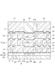
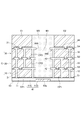
- FIG. 1 is a schematic cross-sectional view for explaining the structure of the coil component 1 according to the embodiment of the present invention.
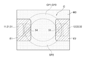
- FIG. 2 is a schematic plan view transparently showing the appearance of the coil component 1 as viewed from the axial direction.
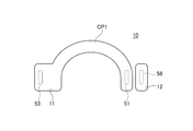
- FIG. 3 is a schematic plan view for explaining the pattern shape of the conductor layer 10.
- FIG. 4 is a schematic plan view for explaining the pattern shape of the conductor layer 20.
- FIG. 5 is a schematic plan view for explaining the pattern shape of the conductor layer 30.
- FIG. 6 is a process diagram for explaining a manufacturing method of the coil component 1.
- FIG. 7 is a process diagram for explaining a manufacturing method of the coil component 1.
- FIG. 8 is a process diagram for explaining a manufacturing method of the coil component 1.
- FIG. 1 is a schematic cross-sectional view for explaining the structure of the coil component 1 according to the embodiment of the present invention.
- FIG. 2 is a schematic plan view transparently showing the appearance of the coil component 1 as viewed from the axial direction.
- FIG. 9 is a process diagram for explaining a manufacturing method of the coil component 1.
- FIG. 10 is a process diagram for explaining a method of manufacturing the coil component 1.
- FIG. 11 is a process diagram for explaining a method of manufacturing the coil component 1.
- FIG. 12 is a process diagram for explaining a method of manufacturing the coil component 1.
- FIG. 13 is a process diagram for explaining a manufacturing method of the coil component 1.
- FIG. 14 is a process diagram for explaining a manufacturing method of the coil component 1.
- FIG. 15 is a process diagram for explaining a manufacturing method of the coil component 1.
- FIG. 16 is a process diagram for explaining a method of manufacturing the coil component 1.
- FIG. 17 is a process diagram for explaining a manufacturing method of the coil component 1.
- FIG. 18 is a process diagram for explaining a method of manufacturing the coil component 1.
- FIG. 10 is a process diagram for explaining a method of manufacturing the coil component 1.
- FIG. 11 is a process diagram for explaining a method of manufacturing the coil component 1.
- FIG. 19 is a process diagram for explaining a method of manufacturing the coil component 1.
- FIG. 20 is a process diagram for explaining a method of manufacturing the coil component 1.
- FIG. 21 is a process diagram for explaining a method of manufacturing the coil component 1.
- FIG. 22 is a process diagram for explaining a method of manufacturing the coil component 1.
- FIG. 23 is a process diagram for explaining the manufacturing method of the coil component 1.
- FIG. 24 is a process diagram for explaining the manufacturing method of the coil component 1.
- FIG. 256 is a process diagram for explaining a method of manufacturing the coil component 1.
- FIG. 26 is a process diagram for explaining a method of manufacturing the coil component 1.
- FIG. 27 is a process diagram for explaining the manufacturing method of the coil component 1.
- FIG. 28 is a process diagram for explaining the manufacturing method of the coil component 1.
- FIG. 20 is a process diagram for explaining a method of manufacturing the coil component 1.
- FIG. 21 is a process diagram for explaining a method of manufacturing the coil component 1.
- FIG. 22 is
- FIG. 29 is a process diagram for explaining the manufacturing method of the coil component 1.
- FIG. 30 is a process diagram for explaining a manufacturing method of the coil component 1.
- FIG. 31 is a process diagram for explaining the manufacturing method of the coil component 1.
- FIG. 32 is a process diagram for explaining a method of manufacturing the coil component 1.
- FIG. 33 is a process diagram for explaining the manufacturing method of the coil component 1.
- FIG. 34 is a process diagram for explaining the manufacturing method of the coil component 1.
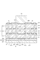
- FIG. 1 is a schematic cross-sectional view for explaining the structure of the coil component 1 according to the embodiment of the present invention. Further, FIG. 2 is a schematic plan view transparently showing the appearance of the coil component 1 as viewed from the axial direction.
- the coil component 1 is a surface mount type chip component suitable to be used as an inductor for a power supply circuit, and as shown in FIGS. 1 and 2, magnetic elements M1 to M3 and magnetic elements M1 to M3. It includes a coil portion C embedded in magnetic elements M1 to M3. The configuration of the coil portion C will be described later, but in the present embodiment, three conductor layers having a spiral coil pattern are laminated, whereby one coil conductor is formed. Then, one end of the coil conductor is connected to the first external terminal E1, and the other end of the coil conductor is connected to the second external terminal E2.
- the magnetic elements M1 to M3 are composite members including a metallic magnetic filler made of iron (Fe) or a permalloy-based material and a resin binder, and form a magnetic path of magnetic flux generated by passing an electric current through the coil portion C.
- a resin binder it is preferable to use a liquid or powder epoxy resin.
- the materials constituting the magnetic elements M1 to M3 may be the same as each other or may be different from each other.
- the magnetic element M1 is a portion (first portion) embedded in the inner diameter region of the coil portion C
- the magnetic element M2 is a portion (second portion) that covers the coil portion C from one side in the axial direction.
- the magnetic element M3 is a portion (third portion) that covers the coil portion C from the other side in the axial direction.
- the coil portion C has a structure in which the interlayer insulating films 41 to 44 and the conductor layers 10, 20, and 30 are alternately laminated.
- the conductor layers 10, 20 and 30 have spiral coil patterns CP1 to CP3, respectively, and the upper surface or the lower surface of the coil patterns CP1 to CP3 is covered with the interlayer insulating films 41 to 44.
- the side surfaces of the coil patterns CP1 to CP3 are covered with a part of the interlayer insulating films 42 to 44, respectively.
- the upper surface and the lower surface of the coil patterns CP1 to CP3 refer to a surface perpendicular to the coil shaft, and the side surfaces of the coil patterns CP1 to CP3 refer to a surface horizontal to the coil shaft.
- the coil patterns CP1 to CP3 form the coil portion C by being connected to each other via through holes formed in the interlayer insulating films 42 and 43.
- Copper (Cu) is preferably used as the material for the conductor layers 10, 20 and 30.
- a non-magnetic material is used for at least the interlayer insulating films 42 and 43.
- a magnetic material may be used for the interlayer insulating film 41 located at the bottom layer and the interlayer insulating film 44 located at the top layer.
- the conductor layer 10 is a first-layer conductor layer formed on the upper surface of the magnetic element M2 via an interlayer insulating film 41, and includes a seed layer S1 as a base.
- the conductor layer 10 is provided with a coil pattern CP1 wound spirally for 0.5 turns and two electrode patterns 11 and 12.
- the lower surface of the coil pattern CP1 is covered with the interlayer insulating film 41, and the side surfaces and the upper surface of the coil pattern CP1 are covered with the interlayer insulating film 42.
- the coil pattern CP1 and the electrode pattern 11 are connected in a predetermined cross section.
- the electrode pattern 12 is provided independently of the coil pattern CP1.
- the electrode pattern 11 is exposed from the magnetic element M3, and its surface is used as a side electrode having the same potential as the external terminal E1.
- the electrode pattern 12 is exposed from the magnetic element M3, and its surface is used as a side electrode having the same potential as the external terminal E2.
- the conductor layer 20 is a second conductor layer formed on the upper surface of the conductor layer 10 via an interlayer insulating film 42, and includes a seed layer S2 as a base.
- the conductor layer 20 is provided with a coil pattern CP2 spirally wound for 0.5 turns and two electrode patterns 21 and 22.
- the lower surface of the coil pattern CP2 is covered with the interlayer insulating film 42, and the side surface and the upper surface of the coil pattern CP2 are covered with the interlayer insulating film 43.
- the electrode patterns 21 and 22 are provided independently of the coil pattern CP2.
- the electrode pattern 21 is exposed from the magnetic element M3, and its surface is used as a side electrode having the same potential as the external terminal E1.
- the electrode pattern 22 is exposed from the magnetic element M3, and its surface is used as a side electrode having the same potential as the external terminal E2.
- the conductor layer 30 is a third conductor layer formed on the upper surface of the conductor layer 20 via an interlayer insulating film 43, and includes a seed layer S3 as a base.
- the conductor layer 30 is provided with a coil pattern CP3 spirally wound for 0.5 turns and two electrode patterns 31 and 32.
- the lower surface of the coil pattern CP3 is covered with the interlayer insulating film 43, and the side surface and the upper surface of the coil pattern CP3 are covered with the interlayer insulating film 44.
- the coil pattern CP3 and the electrode pattern 32 are connected in a predetermined cross section.
- the electrode pattern 31 is provided independently of the coil pattern CP3.
- the electrode pattern 31 is exposed from the magnetic element M3, and its surface is used as a side electrode having the same potential as the external terminal E1.
- the electrode pattern 32 is exposed from the magnetic element M3, and its surface is used as a side electrode having the same potential as the external terminal E2.
- the coil pattern CP1 and the coil pattern CP2 are connected via a via conductor 51 which is a part of the conductor layer 20 and is provided so as to penetrate the interlayer insulating film 42. Further, the coil pattern CP2 and the coil pattern CP3 are connected via a via conductor 52 which is a part of the conductor layer 30 and is provided so as to penetrate the interlayer insulating film 43. As a result, the coil conductors of 1.5 turns are formed by the coil patterns CP1 to CP3. Further, the electrode patterns 11, 21, and 31 are commonly connected to the external terminal E1 via the via conductors 53 to 55, and the electrode patterns 12, 22, and 32 are common to the external terminals E2 via the via conductors 56 to 58. Connected to. As a result, one end of the coil conductor composed of the coil patterns CP1 to CP3 is connected to the external terminal E1 and the other end is connected to the external terminal E2.
- the film thickness of the interlayer insulating film 41 is thinner than that of the interlayer insulating films 42 to 44, whereby the height is reduced.
- the interlayer insulating films 41 to 44 need to have a certain film thickness, but the coil portion C is manufactured for the interlayer insulating film 41 located at the bottom layer. After that, by reducing the film thickness by ashing or the like before forming the magnetic element M2, it is possible to make the film thinner than the interlayer insulating films 42 to 44.
- the protruding portion 41A which is a part of the interlayer insulating film 41
- the protruding portion 44A which is a part of the interlayer insulating film 44
- the opening diameter of the interlayer insulating films 41 and 44 is increased as compared with the case where the protruding portions 41A and 44A project linearly in the radial direction, so that the magnetic characteristics are enhanced.
- the bending angle ⁇ 1 of the protruding portion 41A is larger than the bending angle ⁇ 4 of the protruding portion 44A ( ⁇ 1> ⁇ 4). That is, the protruding portion 41A is curved more than the protruding portion 44A. As described above, such a structure is obtained by making the film thickness of the interlayer insulating film 41 thinner than the film thickness of the interlayer insulating films 42 to 44. By bending the protruding portion 41A to a larger extent, the opening diameter of the interlayer insulating film 41 is further expanded, so that the magnetic characteristics can be further improved.
- the corner portion 41B in which the protruding portion 41A and the vertical portion of the interlayer insulating film 42 are in contact with each other is narrowed, and the protruding portion 44A and the vertical portion of the interlayer insulating film 44 are in contact with each other.
- the corner 44B becomes narrower. As a result, it becomes difficult for the magnetic filler having a large diameter to enter the corner portions 41B and 44B, so that it is possible to suppress the generation of voids due to the magnetic filler having a large diameter entering the corner portions 41B and 44B.
- the amount of protrusion of the protruding portions 41A and 44A is preferably smaller than the maximum diameter of the magnetic filler contained in the magnetic elements M1 to M3. According to this, voids are less likely to be generated in the corner portions 41B and 44B.
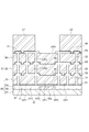
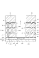
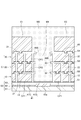
- FIGS. 6 to 34 are process diagrams for explaining the manufacturing method of the coil component 1 according to the present embodiment.
- the process diagrams shown in FIGS. 6 to 34 show a cross section corresponding to one coil component 1, but in reality, a large number of coil components 1 are taken by simultaneously manufacturing a large number of coil components 1 using an assembly substrate. can do.
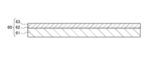
- a support 60 provided with metal foils 62 and 63 such as copper (Cu) on the surface of the base material 61 is prepared (FIG. 6).
- a release layer is provided at the interface between the metal foil 62 and the metal foil 63.
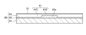
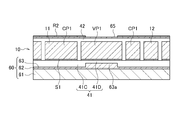
- a protrusion 63a is formed on the metal foil 63 (FIG. 7).
- the interlayer insulating film 41 and the metal foil 64 are formed on the surface of the metal foil 63 provided with the protrusion 63a (FIG. 8).
- the interlayer insulating film 41 and the metal foil 64 can be formed by a laminating method.
- the shape of the protrusion 63a is transferred to the interlayer insulating film 41, and the interlayer insulating film 41 is formed with a thick region 41C and a thin region 41D.
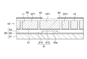
- the seed layer S1 is formed on the surface of the interlayer insulating film 41 by electroless plating (FIG. 10).
- the metal foil 64 may be used as it is as the seed layer, but since it is desirable that the seed layer S1 is as thin as possible, after removing the metal foil 64, the thinner seed layer S1 is used. It is preferable to form a new film.
- a resist pattern R1 is formed on the surface of the seed layer S1 (FIG. 11).
- the resist pattern R1 is a negative pattern of the conductor layer 10.
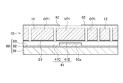
- the conductor layer 10 is formed by growing the seed layer S1 by electrolytic plating (FIG. 12).
- the sacrificial pattern VP1 is formed in the inner diameter region and the outer region of the coil pattern CP1.
- the portion located in the inner diameter region of the coil pattern CP1 is resisted so that the thin region 41D of the interlayer insulating film 41 completely overlaps and the thick region 41C partially overlaps.
- the position of the pattern R1 is adjusted.
- the seed layer S1 exposed on the peeled portion of the resist pattern R1 is removed by etching (FIG. 14).
- the coil pattern CP1 and the sacrificial pattern VP1 are electrically separated by the spiral slit SL.
- an interlayer insulating film 42 and a metal foil 65 are formed on the surface of the conductor layer 10 so as to fill the slit SL (FIG. 15).
- the interlayer insulating film 42 and the metal foil 65 can be formed by a laminating method.
- a resist pattern R2 is formed on the surface of the metal foil 65 (FIG. 16), and the metal leaf 65 is etched using the resist pattern R2 as a mask (FIG. 17). As a result, the metal leaf 65 at the portion overlapping the sacrificial pattern VP1 is removed.
- the sacrificial pattern VP1 is exposed by blasting with the metal foil 65 as a mask (FIG. 19).
- an opening 42a is formed in the interlayer insulating film 42 by laser processing. The opening 42a is provided at a position where the via conductors 51, 53, 56 shown in FIG. 3 should be formed.
- the conductor layer 20, the interlayer insulating film 43, the conductor layer 30, and the interlayer insulating film 44 are sequentially formed.
- the resist pattern R3 is formed on the surface of the seed layer S4 (FIG. 23).
- the seed layers S4 are grown by electrolytic plating to form the external terminals E1 and E2 (FIG. 24).
- the resist pattern R3 is peeled off, and the seed layer S4 exposed on the peeled portion of the resist pattern R3 is removed by etching (FIG. 25).
- the external terminals E1 and E2 are covered with the resist pattern R4 (FIG. 26), and the sacrificial patterns VP1 to VP3 are removed by performing wet etching in this state (FIG. 27). Since the coil patterns CP1 to CP3 are covered with the interlayer insulating films 41 to 44, they are not etched. As a result, a space S is formed in the inner diameter region and the outer region of the coil patterns CP1 to CP3.
- the magnetic elements M1 and M3 that fill this space S are formed (FIG. 28).
- the magnetic elements M1 and M3 are strongly pressed toward the support 60 side so that voids do not occur.
- the protruding portion 44A which is a part of the interlayer insulating film 44, is curved in the pressing direction.
- the support 60 is removed by peeling off the interface between the metal foil 62 and the metal foil 63, and the external terminals E1 and E2 are exposed by grinding the surface of the magnetic element M3 (FIG. 29).
- the metal foil 63 is removed by etching (FIG. 31).
- the film thickness of the interlayer insulating film 41 is reduced as a whole (FIG. 32).
- the amount of decrease in film thickness is adjusted so that all the thin region 41D is removed and the thick region 41C remains.
- the magnetic element M1 embedded in the inner diameter region of the coil portion C is exposed, and the protruding portion 41A is formed on the interlayer insulating film 41.
- the magnetic element M2 is formed so as to cover the interlayer insulating film 41 (FIG. 33).
- the magnetic element M2 is strongly pressed toward the support 70 side so that voids and the like are not generated.
- the protruding portion 41A which is a part of the interlayer insulating film 41, is curved in the pressing direction.
- the coil component 1 according to the present embodiment is completed (FIG. 34).
- the magnetic elements M1 to M3 in the semi-cured state are pressed, and after pressing, the magnetic elements M1 to M3 are completely cured. It doesn't matter.
- the magnetic elements M1 to M3 are strongly pressed so that the protruding portions 41A and 44A, which are a part of the interlayer insulating films 41 and 44, are curved inward. Compared with the case where the projecting portions 41A and 44A project linearly, the entrance of the magnetic path located in the inner diameter region can be widened.
- the interlayer insulating film 41 is laminated on the surface of the metal foil 63 provided with the protrusion 63a, the shape of the protrusion 63a is transferred to the interlayer insulating film 41. As a result, the thick-thickness region 41C and the thin-thickness region 41D are formed in the interlayer insulating film 41. Therefore, the thickness of the interlayer insulating film 41 can be further reduced by the ashing treatment shown in FIG. 32. It becomes. As a result, the height of the coil component 1 can be reduced, and the protrusion 41A can be bent more greatly.
Landscapes
- Engineering & Computer Science (AREA)
- Power Engineering (AREA)
- Microelectronics & Electronic Packaging (AREA)
- Manufacturing & Machinery (AREA)
- Coils Or Transformers For Communication (AREA)
- Manufacturing Cores, Coils, And Magnets (AREA)
Abstract
【課題】スパイラル状のコイルパターンと磁性素体の間に層間絶縁膜が設けられた構造を有するコイル部品の磁気特性を高める。 【解決手段】コイル部品1は、コイルパターンCP1~CP3を軸方向における一方側から覆う層間絶縁膜41と、コイルパターンCP1~CP3の内径領域に埋め込まれた磁性素体M1と、層間絶縁膜41を介してコイルパターンCP1~CP3を軸方向における一方側から覆う磁性素体M2とを備える。層間絶縁膜41は、内径領域に向かって径方向に突出した突出部41Aを有し、突出部41Aは軸方向における他方側に向かって湾曲している。このように、突出部41Aが軸方向に湾曲していることから、内径領域に向かって直線的に突出する場合と比べて、内径領域に位置する磁路の入り口が広がる。このため、突出部41Aに起因する磁気特性の低下が抑えられる。
Description
本発明はコイル部品及びその製造方法に関し、特に、スパイラル状のコイルパターンが磁性素体で覆われた構造を有するコイル部品及びその製造方法に関する。
スパイラル状のコイルパターンを有するチップ型のコイル部品は、インダクタンスを高めるために磁性素体で覆われることがある。例えば、特許文献1には、スパイラル状のコイルパターンが磁性素体で覆われた構造を有するコイル部品が開示されている。
しかしながら、磁性素体を構成する材料は、樹脂材料などと比べると絶縁性が不十分である。このため、コイルパターンを磁性素体によって直接覆うのではなく、コイルパターンを樹脂材料からなる層間絶縁膜で覆い、さらにその表面を磁性素体で覆う構造が採られる。
コイルパターンと磁性素体の間に層間絶縁膜を設けると、特許文献1に記載されているように、層間絶縁膜の一部がコイルパターンの内径領域に突出する。特に、軸方向における端部に位置する層間絶縁膜が内径領域へ大きく突出すると、その分、内径領域に位置する磁路の入り口が狭くなり、磁気特性が低下するという問題があった。
したがって、本発明は、スパイラル状のコイルパターンと磁性素体の間に層間絶縁膜が設けられた構造を有するコイル部品において、層間絶縁膜が内径領域へ突出することに起因する磁気特性の低下を抑制することを目的とする。また、本発明は、このようなコイル部品の製造方法を提供することを目的とする。
本発明によるコイル部品は、スパイラル状に巻回されたコイルパターンと、コイルパターンを軸方向における一方側から覆う第1の層間絶縁膜と、コイルパターンの内径領域に埋め込まれた第1の部分と第1の層間絶縁膜を介してコイルパターンを軸方向における一方側から覆う第2の部分を含む磁性素体とを備え、第1の層間絶縁膜は、内径領域に向かって径方向に突出した第1の突出部を有し、第1の突出部は、軸方向における他方側に向かって湾曲していることを特徴とする。
本発明によれば、第1の突出部が軸方向に湾曲していることから、内径領域に向かって直線的に突出する場合と比べて、内径領域に位置する磁路の入り口が広がる。このため、第1の突出部に起因する磁気特性の低下を抑えることが可能となる。
本発明によるコイル部品は、コイルパターンを軸方向における他方側から覆う第2の層間絶縁膜をさらに備え、磁性素体は、第2の層間絶縁膜を介してコイルパターンを軸方向における他方側から覆う第3の部分をさらに含むものであっても構わない。これによれば、より高い磁気特性を得ることが可能となる。
本発明によるコイル部品は、第2の層間絶縁膜に設けられた開口部を介して、それぞれコイルパターンの一端及び他端に接続された第1及び第2の外部端子をさらに備え、第1の層間絶縁膜は、第2の層間絶縁膜よりも膜厚が薄くても構わない。これによれば、外部端子とは反対側に位置する第1の層間絶縁膜の膜厚が薄いことから、コイル部品を低背化することが可能となる。
本発明において、第2の層間絶縁膜は内径領域に向かって径方向に突出した第2の突出部を有し、第2の突出部は軸方向における一方側に向かって湾曲していても構わない。これによれば、第2の突出部が軸方向に湾曲していることから、内径領域に向かって直線的に突出する場合と比べて、内径領域に位置する磁路の入り口が広がる。このため、突出部に起因する磁気特性の低下を抑えることが可能となる。
本発明において、第1の突出部は第2の突出部よりも大きく湾曲していても構わない。これによれば、第1の突出部に起因する磁気特性の低下をより抑えることが可能となる。
本発明において、磁性素体は磁性フィラーと樹脂バインダーを含む複合部材であり、第1の突出部の突出量は、磁性フィラーの最大径よりも小さくても構わない。これによれば、第1の突出部の近傍にボイドが生じにくくなる。
本発明によるコイル部品の製造方法は、スパイラル状に巻回され、軸方向における一方側が層間絶縁膜で覆われたコイルパターンを形成する第1の工程と、層間絶縁膜にコイルパターンの内径領域に向かって径方向に突出した突出部を形成する第2の工程と、磁性素体をコイルパターンの内径領域に埋め込むとともに、層間絶縁膜を介してコイルパターンを軸方向における一方側から磁性素体で覆う第3の工程とを備え、第3の工程においては、第1の突出部が軸方向における他方側に向かって湾曲するよう、磁性素体を軸方向における他方側に押圧することを特徴とする。
本発明によれば、磁性素体を押圧することによって突出部を湾曲させていることから、内径領域に位置する磁路の入り口を広げることが可能となる。これにより、突出部に起因する磁気特性の低下を抑えることが可能となる。
本発明において、第1の工程は、軸方向から見てコイルパターンの内径領域と重なる部分に膜厚の厚い領域と薄い領域が含まれるよう、層間絶縁膜を形成する工程を含み、第2の工程は、層間絶縁膜の膜厚を全体的に減少させることにより膜厚の薄い領域を除去し、これによって突出部を形成しても構わない。これによれば、突出部の厚みを薄くすることができるため、突出部をより大きく湾曲させることが可能となる。
このように、本発明によれば、スパイラル状のコイルパターンが磁性素体で覆われた構造を有するコイル部品において、層間絶縁膜が内径領域へ突出することに起因する磁気特性の低下を抑制することが可能となる。また、本発明によれば、このようなコイル部品の製造方法を提供することが可能となる。
以下、添付図面を参照しながら、本発明の好ましい実施形態について詳細に説明する。
図1は、本発明の一実施形態によるコイル部品1の構造を説明するための略断面図である。また、図2は、コイル部品1を軸方向から見た外観を透過的に示す略平面図である。
本発明の一実施形態によるコイル部品1は、電源回路用のインダクタとして用いることが好適な表面実装型のチップ部品であり、図1及び図2に示すように、磁性素体M1~M3と、磁性素体M1~M3に埋め込まれたコイル部Cとを備える。コイル部Cの構成については後述するが、本実施形態においてはスパイラル状のコイルパターンを有する導体層が3層積層され、これによって1つのコイル導体が形成される。そして、コイル導体の一端が第1の外部端子E1に接続され、コイル導体の他端が第2の外部端子E2に接続される。
磁性素体M1~M3は、鉄(Fe)やパーマロイ系材料などからなる金属磁性フィラーと樹脂バインダーを含む複合部材であり、コイル部Cに電流を流すことによって生じる磁束の磁路を構成する。樹脂バインダーとしては、液状又は粉体のエポキシ樹脂を用いることが好ましい。磁性素体M1~M3を構成する材料は、互いに同じであっても構わないし、互いに異なっていても構わない。ここで、磁性素体M1はコイル部Cの内径領域に埋め込まれた部分(第1の部分)であり、磁性素体M2はコイル部Cを軸方向における一方側から覆う部分(第2の部分)であり、磁性素体M3はコイル部Cを軸方向における他方側から覆う部分(第3の部分)である。
図1に示すように、コイル部Cは層間絶縁膜41~44と導体層10,20,30が交互に積層された構成を有している。導体層10,20,30はそれぞれスパイラル状のコイルパターンCP1~CP3を有しており、コイルパターンCP1~CP3の上面又は下面が層間絶縁膜41~44で覆われている。コイルパターンCP1~CP3の側面は、それぞれ層間絶縁膜42~44の一部で覆われている。ここで、コイルパターンCP1~CP3の上面及び下面とは、コイル軸に対して垂直な面を指し、コイルパターンCP1~CP3の側面とは、コイル軸に対して水平な面を指す。
コイルパターンCP1~CP3は、層間絶縁膜42,43に形成されたスルーホールを介して互いに接続されることにより、コイル部Cを構成している。導体層10,20,30の材料としては、銅(Cu)を用いることが好ましい。層間絶縁膜41~44のうち、少なくとも層間絶縁膜42,43については非磁性材料が用いられる。最下層に位置する層間絶縁膜41及び最上層に位置する層間絶縁膜44については、磁性材料を用いても構わない。
導体層10は、磁性素体M2の上面に層間絶縁膜41を介して形成された1層目の導体層であり、下地であるシード層S1を含んでいる。図3に示すように、導体層10には、スパイラル状に0.5ターン巻回されたコイルパターンCP1と、2つの電極パターン11,12が設けられている。コイルパターンCP1の下面は層間絶縁膜41で覆われ、コイルパターンCP1の側面及び上面は層間絶縁膜42で覆われている。図1及び図3に示すように、所定の断面においては、コイルパターンCP1と電極パターン11が接続されている。これに対し、電極パターン12はコイルパターンCP1とは独立して設けられている。電極パターン11は磁性素体M3から露出しており、その表面は外部端子E1と同電位の側面電極として用いられる。同様に、電極パターン12は磁性素体M3から露出しており、その表面は外部端子E2と同電位の側面電極として用いられる。
導体層20は、導体層10の上面に層間絶縁膜42を介して形成された2層目の導体層であり、下地であるシード層S2を含んでいる。図4に示すように、導体層20には、スパイラル状に0.5ターン巻回されたコイルパターンCP2と、2つの電極パターン21,22が設けられている。コイルパターンCP2の下面は層間絶縁膜42で覆われ、コイルパターンCP2の側面及び上面は層間絶縁膜43で覆われている。電極パターン21,22は、いずれもコイルパターンCP2とは独立して設けられている。電極パターン21は磁性素体M3から露出しており、その表面は外部端子E1と同電位の側面電極として用いられる。同様に、電極パターン22は磁性素体M3から露出しており、その表面は外部端子E2と同電位の側面電極として用いられる。
導体層30は、導体層20の上面に層間絶縁膜43を介して形成された3層目の導体層であり、下地であるシード層S3を含んでいる。図5に示すように、導体層30には、スパイラル状に0.5ターン巻回されたコイルパターンCP3と、2つの電極パターン31,32が設けられている。コイルパターンCP3の下面は層間絶縁膜43で覆われ、コイルパターンCP3の側面及び上面は層間絶縁膜44で覆われている。図1に示すように、所定の断面においては、コイルパターンCP3と電極パターン32が接続されている。これに対し、電極パターン31はコイルパターンCP3とは独立して設けられている。電極パターン31は磁性素体M3から露出しており、その表面は外部端子E1と同電位の側面電極として用いられる。同様に、電極パターン32は磁性素体M3から露出しており、その表面は外部端子E2と同電位の側面電極として用いられる。
そして、コイルパターンCP1とコイルパターンCP2は、導体層20の一部であり層間絶縁膜42を貫通して設けられたビア導体51を介して接続される。また、コイルパターンCP2とコイルパターンCP3は、導体層30の一部であり層間絶縁膜43を貫通して設けられたビア導体52を介して接続される。これにより、コイルパターンCP1~CP3によって1.5ターンのコイル導体が形成される。また、電極パターン11,21,31は、ビア導体53~55を介して外部端子E1に共通に接続され、電極パターン12,22,32は、ビア導体56~58を介して外部端子E2に共通に接続される。これにより、コイルパターンCP1~CP3からなるコイル導体の一端が外部端子E1に接続され、他端が外部端子E2に接続された構成が得られる。
本実施形態においては、層間絶縁膜41の膜厚が層間絶縁膜42~44よりも薄く、これにより低背化が図られている。後述する各プロセスを実施するためには、層間絶縁膜41~44の膜厚としてはある程度の膜厚が必要であるが、最下層に位置する層間絶縁膜41については、コイル部Cを作製した後、磁性素体M2を形成する前にアッシング等により膜厚を減少させることにより、層間絶縁膜42~44よりも薄くすることが可能である。
さらに、本実施形態においては、層間絶縁膜41~44の一部がコイル部Cの内径領域に突出している。このうち、層間絶縁膜41の一部である突出部41Aと層間絶縁膜44の一部である突出部44Aは、コイル部Cの中心に向かって湾曲した形状を有している。つまり、突出部41Aは磁性素体M3側に向かって図1の上方向に湾曲し、突出部44Aは磁性素体M2側に向かって図1の下方向に湾曲している。これにより、突出部41A,44Aが径方向に直線的に突出する場合と比べて、層間絶縁膜41,44の開口径が拡大することから、磁気特性が高められる。
また、本実施形態においては、突出部41Aの湾曲角度θ1が突出部44Aの湾曲角度θ4よりも大きい(θ1>θ4)。つまり、突出部41Aの方が突出部44Aよりも大きく湾曲している。このような構造は、上述の通り、層間絶縁膜41の膜厚を層間絶縁膜42~44の膜厚よりも薄くすることにより得られる。突出部41Aをより大きく湾曲させることにより、層間絶縁膜41の開口径がより拡大することから、より磁気特性を高めることができる。
さらに、突出部41A,44Aが湾曲していることにより、突出部41Aと層間絶縁膜42の垂直部分が接する角部41Bが狭くなり、且つ、突出部44Aと層間絶縁膜44の垂直部分が接する角部44Bが狭くなる。これにより、角部41B,44Bに径の大きな磁性フィラーが入り込みにくくなることから、角部41B,44Bに径の大きな磁性フィラーが入り込むことによるボイドの発生を抑えることが可能となる。特に、突出部41A,44Aの突出量は、磁性素体M1~M3に含まれる磁性フィラーの最大径よりも小さいことが好ましい。これによれば、角部41B,44Bにボイドがより発生しにくくなる。
次に、本実施形態によるコイル部品1の製造方法について説明する。
図6~図34は、本実施形態によるコイル部品1の製造方法を説明するための工程図である。図6~図34に示す工程図は、1個のコイル部品1に対応する断面を示しているが、実際には、集合基板を用いて多数のコイル部品1を同時に作製することによって多数個取りすることができる。
まず、基材61の表面に銅(Cu)などの金属箔62,63が設けられた支持体60を用意する(図6)。金属箔62と金属箔63の界面には剥離層が設けられている。次に、金属箔63をパターニングすることによって、金属箔63に突起部63aを形成する(図7)。
次に、突起部63aが設けられた金属箔63の表面に、層間絶縁膜41及び金属箔64を形成する(図8)。層間絶縁膜41及び金属箔64の形成は、ラミネート法によって行うことができる。これにより、突起部63aの形状が層間絶縁膜41に転写され、層間絶縁膜41には膜厚の厚い領域41Cと膜厚の薄い領域41Dが形成される。
次に、エッチングにより金属箔64を除去した後(図9)、無電解メッキによって層間絶縁膜41の表面にシード層S1を形成する(図10)。シード層S1を形成する代わりに、金属箔64をそのままシード層として用いても構わないが、シード層S1はできる限り薄いことが望ましいため、金属箔64を除去した後、より薄いシード層S1を新たに成膜することが好ましい。
次に、シード層S1の表面にレジストパターンR1を形成する(図11)。レジストパターンR1は、導体層10のネガパターンである。この状態で、電解メッキによってシード層S1を成長させることにより、導体層10を形成する(図12)。この時、コイルパターンCP1の内径領域及び外側領域には、犠牲パターンVP1が形成される。犠牲パターンVP1のうち、コイルパターンCP1の内径領域に位置する部分は、層間絶縁膜41のうち膜厚の薄い領域41Dが完全に重なり、且つ、膜厚の厚い領域41Cが一部重なるよう、レジストパターンR1の位置が調整される。
次に、レジストパターンR1を剥離した後(図13)、レジストパターンR1の剥離部分に露出するシード層S1をエッチングにより除去する(図14)。これにより、コイルパターンCP1と犠牲パターンVP1がスパイラル状のスリットSLによって電気的に分離される。次に、スリットSLを埋めるよう、導体層10の表面に層間絶縁膜42及び金属箔65を形成する(図15)。層間絶縁膜42及び金属箔65の形成は、ラミネート法によって行うことができる。次に、金属箔65の表面にレジストパターンR2を形成し(図16)、レジストパターンR2をマスクとして金属箔65をエッチングする(図17)。これにより、犠牲パターンVP1と重なる部分の金属箔65が除去される。
次に、レジストパターンR2を剥離した後(図18)、金属箔65をマスクとしてブラスト加工することにより、犠牲パターンVP1を露出させる(図19)。次に、金属箔65を除去した後(図20)、レーザー加工によって層間絶縁膜42に開口部42aを形成する。開口部42aは、図3に示すビア導体51,53,56を形成すべき箇所に設けられる。以上の工程により、導体層10及び層間絶縁膜42の形成が完了する。
その後、図10~図21に示す工程を繰り返すことにより、導体層20、層間絶縁膜43、導体層30、層間絶縁膜44を順次形成する。次に、層間絶縁膜44の表面にシード層S4を形成した後(図22)、シード層S4の表面にレジストパターンR3を形成する(図23)。この状態で、電解メッキによってシード層S4を成長させることにより、外部端子E1,E2を形成する(図24)。その後、レジストパターンR3を剥離し、レジストパターンR3の剥離部分に露出するシード層S4をエッチングにより除去する(図25)。
次に、外部端子E1,E2をレジストパターンR4で覆い(図26)、この状態でウェットエッチングを行うことにより、犠牲パターンVP1~VP3を除去する(図27)。コイルパターンCP1~CP3については、層間絶縁膜41~44で覆われているため、エッチングされることはない。これにより、コイルパターンCP1~CP3の内径領域及び外側領域には、空間Sが形成される。
次に、この空間Sを埋める磁性素体M1,M3を形成する(図28)。磁性素体M1,M3の形成においては、ボイドが生じないよう、支持体60側に向けて磁性素体M1,M3を強く押圧する。これにより、層間絶縁膜44の一部である突出部44Aは、押圧方向に向けて湾曲する。次に、金属箔62と金属箔63の界面を剥離することによって支持体60を除去し、さらに、磁性素体M3の表面を研削することによって外部端子E1,E2を露出させる(図29)。次に、上下反転させて支持体70を貼り付けた後(図30)、エッチングにより金属箔63を除去する(図31)。この状態でアッシング処理を行うことにより、層間絶縁膜41の膜厚を全体的に減少させる(図32)。膜厚の減少量は、膜厚の薄い領域41Dが全て除去され、且つ、膜厚の厚い領域41Cが残存する量に調整する。これにより、コイル部Cの内径領域に埋め込まれた磁性素体M1が露出するとともに、層間絶縁膜41に突出部41Aが形成される。
次に、層間絶縁膜41を覆うように磁性素体M2を形成する(図33)。磁性素体M2の形成においては、ボイドなどが生じないよう、支持体70側に向けて磁性素体M2を強く押圧する。これにより、層間絶縁膜41の一部である突出部41Aは、押圧方向に向けて湾曲する。そして、ダイシングによって個片化すれば、本実施形態によるコイル部品1が完成する(図34)。なお、層間絶縁膜の突出部41A,44Aの湾曲形状を確実に形成するために、半硬化状態の磁性素体M1~M3を押圧し、押圧した後、磁性素体M1~M3を完全硬化させても構わない。
このように、本実施形態においては、層間絶縁膜41,44の一部である突出部41A,44Aが内側に向かって湾曲するよう、磁性素体M1~M3を強く押圧していることから、突出部41A,44Aが直線的に突出する場合と比べて、内径領域に位置する磁路の入り口を広げることが可能となる。
また、本実施形態においては、突起部63aが設けられた金属箔63の表面に層間絶縁膜41をラミネートしていることから、突起部63aの形状が層間絶縁膜41に転写される。これにより、層間絶縁膜41に膜厚の厚い領域41Cと膜厚の薄い領域41Dが形成されることから、図32に示すアッシング処理によって、層間絶縁膜41の膜厚をより薄くすることが可能となる。これにより、コイル部品1を低背化することができるとともに、突出部41Aをより大きく湾曲させることが可能となる。
以上、本発明の好ましい実施形態について説明したが、本発明は、上記の実施形態に限定されることなく、本発明の主旨を逸脱しない範囲で種々の変更が可能であり、それらも本発明の範囲内に包含されるものであることはいうまでもない。
1 コイル部品
10,20,30 導体層
11,12,21,22,31,32 電極パターン
41~44 層間絶縁膜
41A,44A 突出部
41B,44B 角部
41C 厚い領域
41D 薄い領域
42a 開口部
51~58 ビア導体
60 支持体
61 基材
62~65 金属箔
63a 突起部
70 支持体
C コイル部
CP1~CP3 コイルパターン
E1,E2 外部端子
M1~M3 磁性素体
R1~R4 レジストパターン
S 空間
S1~S4 シード層
SL スリット
VP1~VP3 犠牲パターン
10,20,30 導体層
11,12,21,22,31,32 電極パターン
41~44 層間絶縁膜
41A,44A 突出部
41B,44B 角部
41C 厚い領域
41D 薄い領域
42a 開口部
51~58 ビア導体
60 支持体
61 基材
62~65 金属箔
63a 突起部
70 支持体
C コイル部
CP1~CP3 コイルパターン
E1,E2 外部端子
M1~M3 磁性素体
R1~R4 レジストパターン
S 空間
S1~S4 シード層
SL スリット
VP1~VP3 犠牲パターン
Claims (8)
- スパイラル状に巻回されたコイルパターンと、
前記コイルパターンを軸方向における一方側から覆う第1の層間絶縁膜と、
前記コイルパターンの内径領域に埋め込まれた第1の部分と、前記第1の層間絶縁膜を介して前記コイルパターンを前記軸方向における前記一方側から覆う第2の部分を含む磁性素体と、を備え、
前記第1の層間絶縁膜は、前記内径領域に向かって径方向に突出した第1の突出部を有し、
前記第1の突出部は、前記軸方向における他方側に向かって湾曲していることを特徴とするコイル部品。 - 前記コイルパターンを前記軸方向における前記他方側から覆う第2の層間絶縁膜をさらに備え、
前記磁性素体は、前記第2の層間絶縁膜を介して前記コイルパターンを前記軸方向における前記他方側から覆う第3の部分をさらに含むことを特徴とする請求項1に記載のコイル部品。 - 前記第2の層間絶縁膜に設けられた開口部を介して、それぞれ前記コイルパターンの一端及び他端に接続された第1及び第2の外部端子をさらに備え、
前記第1の層間絶縁膜は、前記第2の層間絶縁膜よりも膜厚が薄いことを特徴とする請求項2に記載のコイル部品。 - 前記第2の層間絶縁膜は、前記内径領域に向かって径方向に突出した第2の突出部を有し、
前記第2の突出部は、前記軸方向における前記一方側に向かって湾曲していることを特徴とする請求項3に記載のコイル部品。 - 前記第1の突出部は、前記第2の突出部よりも大きく湾曲していることを特徴とする請求項4に記載のコイル部品。
- 前記磁性素体は、磁性フィラーと樹脂バインダーを含む複合部材であり、
前記第1の突出部の突出量は、前記磁性フィラーの最大径よりも小さいことを特徴とする請求項1乃至5のいずれか一項に記載のコイル部品。 - スパイラル状に巻回され、軸方向における一方側が層間絶縁膜で覆われたコイルパターンを形成する第1の工程と、
前記層間絶縁膜に、前記コイルパターンの内径領域に向かって径方向に突出した突出部を形成する第2の工程と、
磁性素体を前記コイルパターンの前記内径領域に埋め込むとともに、前記層間絶縁膜を介して前記コイルパターンを前記軸方向における前記一方側から磁性素体で覆う第3の工程と、を備え、
前記第3の工程においては、前記第1の突出部が前記軸方向における他方側に向かって湾曲するよう、前記磁性素体を前記軸方向における前記他方側に押圧することを特徴とするコイル部品の製造方法。 - 前記第1の工程は、前記軸方向から見て前記コイルパターンの前記内径領域と重なる部分に膜厚の厚い領域と薄い領域が含まれるよう、前記層間絶縁膜を形成する工程を含み、
前記第2の工程は、前記層間絶縁膜の膜厚を全体的に減少させることにより前記膜厚の薄い領域を除去し、これによって前記突出部を形成することを特徴とする請求項7に記載のコイル部品の製造方法。
Priority Applications (2)
| Application Number | Priority Date | Filing Date | Title |
|---|---|---|---|
| US17/767,226 US12340937B2 (en) | 2019-10-23 | 2020-09-29 | Coil component and manufacturing method therefor |
| CN202080073429.7A CN114568034B (zh) | 2019-10-23 | 2020-09-29 | 线圈部件及其制造方法 |
Applications Claiming Priority (2)
| Application Number | Priority Date | Filing Date | Title |
|---|---|---|---|
| JP2019-192946 | 2019-10-23 | ||
| JP2019192946A JP7362416B2 (ja) | 2019-10-23 | 2019-10-23 | コイル部品及びその製造方法 |
Publications (1)
| Publication Number | Publication Date |
|---|---|
| WO2021079697A1 true WO2021079697A1 (ja) | 2021-04-29 |
Family
ID=75620005
Family Applications (1)
| Application Number | Title | Priority Date | Filing Date |
|---|---|---|---|
| PCT/JP2020/036858 Ceased WO2021079697A1 (ja) | 2019-10-23 | 2020-09-29 | コイル部品及びその製造方法 |
Country Status (4)
| Country | Link |
|---|---|
| US (1) | US12340937B2 (ja) |
| JP (2) | JP7362416B2 (ja) |
| CN (1) | CN114568034B (ja) |
| WO (1) | WO2021079697A1 (ja) |
Families Citing this family (8)
| Publication number | Priority date | Publication date | Assignee | Title |
|---|---|---|---|---|
| US11935678B2 (en) * | 2020-12-10 | 2024-03-19 | GLOBALFOUNDARIES Singapore Pte. Ltd. | Inductive devices and methods of fabricating inductive devices |
| JP7618476B2 (ja) * | 2021-03-29 | 2025-01-21 | Tdk株式会社 | コイル部品及びその製造方法 |
| US20240412917A1 (en) * | 2021-09-30 | 2024-12-12 | Tdk Corporation | Coil component |
| JP7743263B2 (ja) * | 2021-10-22 | 2025-09-24 | Tdk株式会社 | コイル部品の製造方法 |
| JP7548201B2 (ja) * | 2021-12-14 | 2024-09-10 | 株式会社村田製作所 | インダクタ部品およびインダクタ部品の製造方法 |
| JP7548200B2 (ja) * | 2021-12-14 | 2024-09-10 | 株式会社村田製作所 | インダクタ部品およびインダクタ部品の製造方法 |
| JP7842666B2 (ja) * | 2022-09-12 | 2026-04-08 | Tdk株式会社 | コイル部品 |
| CN121909517A (zh) * | 2023-09-26 | 2026-04-21 | Tdk株式会社 | 电子部件及其制造方法 |
Citations (3)
| Publication number | Priority date | Publication date | Assignee | Title |
|---|---|---|---|---|
| WO2016208305A1 (ja) * | 2015-06-24 | 2016-12-29 | 株式会社村田製作所 | コイル部品の製造方法 |
| JP2017107971A (ja) * | 2015-12-09 | 2017-06-15 | 株式会社村田製作所 | インダクタ部品 |
| WO2019044459A1 (ja) * | 2017-08-28 | 2019-03-07 | Tdk株式会社 | コイル部品及びその製造方法 |
Family Cites Families (17)
| Publication number | Priority date | Publication date | Assignee | Title |
|---|---|---|---|---|
| JPH05101938A (ja) * | 1991-10-03 | 1993-04-23 | Murata Mfg Co Ltd | 積層型コイル及びその製造方法 |
| JP2001085232A (ja) * | 1999-09-16 | 2001-03-30 | Tdk Corp | 表面実装用コモンモードチョークコイル |
| JP3724405B2 (ja) * | 2001-10-23 | 2005-12-07 | 株式会社村田製作所 | コモンモードチョークコイル |
| JP4211591B2 (ja) * | 2003-12-05 | 2009-01-21 | 株式会社村田製作所 | 積層型電子部品の製造方法および積層型電子部品 |
| JP2007242800A (ja) * | 2006-03-07 | 2007-09-20 | Tdk Corp | コモンモードフィルタ |
| KR101381016B1 (ko) * | 2010-03-31 | 2014-04-04 | 가부시키가이샤 무라타 세이사쿠쇼 | 전자 부품 및 그 제조 방법 |
| JP5609347B2 (ja) * | 2010-07-13 | 2014-10-22 | トヨタ自動車株式会社 | 巻線 |
| JP6564614B2 (ja) * | 2014-05-22 | 2019-08-21 | 新光電気工業株式会社 | インダクタ及びインダクタの製造方法 |
| JP6500635B2 (ja) | 2015-06-24 | 2019-04-17 | 株式会社村田製作所 | コイル部品の製造方法およびコイル部品 |
| US11024454B2 (en) * | 2015-10-16 | 2021-06-01 | Qualcomm Incorporated | High performance inductors |
| JP6332252B2 (ja) * | 2015-12-09 | 2018-05-30 | トヨタ自動車株式会社 | 受電装置および送電装置 |
| JP6848734B2 (ja) * | 2017-07-10 | 2021-03-24 | Tdk株式会社 | コイル部品 |
| JP2019054117A (ja) * | 2017-09-15 | 2019-04-04 | 日本特殊陶業株式会社 | 配線基板、及びプレーナトランス |
| KR101994758B1 (ko) * | 2017-10-16 | 2019-07-01 | 삼성전기주식회사 | 박막형 인덕터 |
| KR102430636B1 (ko) * | 2018-03-08 | 2022-08-09 | 삼성전기주식회사 | 코일 부품 |
| JP7135923B2 (ja) * | 2019-02-15 | 2022-09-13 | 株式会社村田製作所 | インダクタ部品 |
| JP7180472B2 (ja) * | 2019-03-18 | 2022-11-30 | Tdk株式会社 | コイル部品及びその製造方法 |
-
2019
- 2019-10-23 JP JP2019192946A patent/JP7362416B2/ja active Active
-
2020
- 2020-09-29 US US17/767,226 patent/US12340937B2/en active Active
- 2020-09-29 CN CN202080073429.7A patent/CN114568034B/zh active Active
- 2020-09-29 WO PCT/JP2020/036858 patent/WO2021079697A1/ja not_active Ceased
-
2023
- 2023-10-04 JP JP2023172443A patent/JP7557592B2/ja active Active
Patent Citations (3)
| Publication number | Priority date | Publication date | Assignee | Title |
|---|---|---|---|---|
| WO2016208305A1 (ja) * | 2015-06-24 | 2016-12-29 | 株式会社村田製作所 | コイル部品の製造方法 |
| JP2017107971A (ja) * | 2015-12-09 | 2017-06-15 | 株式会社村田製作所 | インダクタ部品 |
| WO2019044459A1 (ja) * | 2017-08-28 | 2019-03-07 | Tdk株式会社 | コイル部品及びその製造方法 |
Also Published As
| Publication number | Publication date |
|---|---|
| JP7362416B2 (ja) | 2023-10-17 |
| JP2023168523A (ja) | 2023-11-24 |
| CN114568034A (zh) | 2022-05-31 |
| US20220375679A1 (en) | 2022-11-24 |
| JP7557592B2 (ja) | 2024-09-27 |
| US12340937B2 (en) | 2025-06-24 |
| CN114568034B (zh) | 2025-11-25 |
| JP2021068805A (ja) | 2021-04-30 |
Similar Documents
| Publication | Publication Date | Title |
|---|---|---|
| JP7362416B2 (ja) | コイル部品及びその製造方法 | |
| US9520223B2 (en) | Inductor and method for manufacturing the same | |
| JP7471846B2 (ja) | コイル部品及びその製造方法 | |
| KR101832608B1 (ko) | 코일 전자 부품 및 그 제조방법 | |
| US20130300529A1 (en) | Coil structure and electromagnetic component using the same | |
| US8988181B2 (en) | Common mode filter with multi-spiral layer structure and method of manufacturing the same | |
| JP2023062846A (ja) | コイル部品及びその製造方法 | |
| JP2020038940A (ja) | インダクタ及びその製造方法 | |
| CN106992056B (zh) | 线圈部件 | |
| CN109119233A (zh) | 线圈组件及其制造方法 | |
| JP2020136547A (ja) | コイル部品及びその製造方法 | |
| JP6819395B2 (ja) | コイル部品 | |
| JP2020155480A (ja) | コイル部品及びその製造方法 | |
| WO2019235510A1 (ja) | コイル部品及びその製造方法 | |
| JP2017103360A (ja) | コイル部品及び電源回路ユニット | |
| JP7124333B2 (ja) | コイル部品及びその製造方法 | |
| JP7326788B2 (ja) | コイル部品及びその製造方法 | |
| JP2020155511A (ja) | コイル部品 | |
| JP7073650B2 (ja) | コイル部品 | |
| US20250022641A1 (en) | Electronic component and method for manufacturing the same | |
| JP7722902B2 (ja) | コイル部品 | |
| JP2020155510A (ja) | 電子部品 | |
| JP2020136466A (ja) | コイル部品及びその製造方法 | |
| JP2004221177A (ja) | コイル部品 | |
| CN117476341A (zh) | 电感元件及电感元件的制备方法 |
Legal Events
| Date | Code | Title | Description |
|---|---|---|---|
| 121 | Ep: the epo has been informed by wipo that ep was designated in this application |
Ref document number: 20879019 Country of ref document: EP Kind code of ref document: A1 |
|
| NENP | Non-entry into the national phase |
Ref country code: DE |
|
| 122 | Ep: pct application non-entry in european phase |
Ref document number: 20879019 Country of ref document: EP Kind code of ref document: A1 |
|
| WWG | Wipo information: grant in national office |
Ref document number: 17767226 Country of ref document: US |