WO2020255790A1 - 電子機器 - Google Patents
電子機器 Download PDFInfo
- Publication number
- WO2020255790A1 WO2020255790A1 PCT/JP2020/022661 JP2020022661W WO2020255790A1 WO 2020255790 A1 WO2020255790 A1 WO 2020255790A1 JP 2020022661 W JP2020022661 W JP 2020022661W WO 2020255790 A1 WO2020255790 A1 WO 2020255790A1
- Authority
- WO
- WIPO (PCT)
- Prior art keywords
- circuit board
- printed circuit
- shield member
- electronic device
- antenna
- Prior art date
Links
Images


Classifications
-
- H—ELECTRICITY
- H05—ELECTRIC TECHNIQUES NOT OTHERWISE PROVIDED FOR
- H05K—PRINTED CIRCUITS; CASINGS OR CONSTRUCTIONAL DETAILS OF ELECTRIC APPARATUS; MANUFACTURE OF ASSEMBLAGES OF ELECTRICAL COMPONENTS
- H05K9/00—Screening of apparatus or components against electric or magnetic fields
-
- H—ELECTRICITY
- H05—ELECTRIC TECHNIQUES NOT OTHERWISE PROVIDED FOR
- H05K—PRINTED CIRCUITS; CASINGS OR CONSTRUCTIONAL DETAILS OF ELECTRIC APPARATUS; MANUFACTURE OF ASSEMBLAGES OF ELECTRICAL COMPONENTS
- H05K9/00—Screening of apparatus or components against electric or magnetic fields
- H05K9/0007—Casings
- H05K9/002—Casings with localised screening
- H05K9/0022—Casings with localised screening of components mounted on printed circuit boards [PCB]
- H05K9/0024—Shield cases mounted on a PCB, e.g. cans or caps or conformal shields
- H05K9/0032—Shield cases mounted on a PCB, e.g. cans or caps or conformal shields having multiple parts, e.g. frames mating with lids
- H05K9/0033—Shield cases mounted on a PCB, e.g. cans or caps or conformal shields having multiple parts, e.g. frames mating with lids disposed on both PCB faces
-
- H—ELECTRICITY
- H01—ELECTRIC ELEMENTS
- H01Q—ANTENNAS, i.e. RADIO AERIALS
- H01Q1/00—Details of, or arrangements associated with, antennas
- H01Q1/52—Means for reducing coupling between antennas; Means for reducing coupling between an antenna and another structure
- H01Q1/526—Electromagnetic shields
Definitions
- the present invention relates to an electronic device having a built-in printed circuit board.
- ⁇ Generally, electronic devices have a built-in printed circuit board on which various electronic components are mounted. Some of these electronic components generate an electromagnetic field that becomes noise that affects the operation of other electronic components and wireless communication. In order to prevent such noise propagation, a shield member formed of a metal plate or the like covers a circuit element that is a source of noise.
- the present invention has been made in consideration of the above circumstances, and one of the objects thereof is an electron capable of effectively suppressing noise generated from a circuit element arranged on a printed circuit board by a shield member. It is to provide equipment.
- the electronic device includes a printed circuit board on which an electronic component is mounted on the surface thereof, and a shield member arranged so as to face the surface of the printed circuit board and cover the electronic component.
- the shield member has a protruding portion that extends outward beyond one end of the printed circuit board in a plan view, and the protruding portion is bent toward the printed circuit board, and the tip thereof is at least a side surface of the printed circuit board. It is characterized in that it extends to opposite positions.
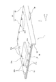
- the electronic device 1 is, for example, a home-use game machine or the like, and is a printed circuit board (printed wiring board) 10 on which various electronic components are mounted and a front shield member attached to the printed circuit board 10. 20, the back side shield member 30, and the antenna 40 are included.
- FIG. 1 is a perspective view showing the state of the surface of the printed circuit board 10 in a state before the front side shield member 20 and the back side shield member 30 are attached.
- FIG. 2 is a perspective view showing a state of the surface of the printed circuit board 10 in a state where the front side shield member 20 and the back side shield member 30 are attached.
- FIG. 3 is a partial cross-sectional view showing a positional relationship of the printed circuit board 10 in a state where the front side shield member 20 and the back side shield member 30 are attached, as viewed from the side.
- At least one electronic component 11 that is a source of noise is arranged on the surface of the printed circuit board 10. Although only one electronic component 11 is shown on the surface side of the printed circuit board 10 in FIG. 1, a plurality of electronic components may be arranged on the surface of the printed circuit board 10. Further, the printed circuit board 10 may be a double-sided printed circuit board, and one or a plurality of electronic components may be arranged on the back surface side as well.
- the front side shield member 20 and the back side shield member 30 are members for shielding electromagnetic waves that become noise radiated from the printed circuit board 10 and electronic components arranged on the printed circuit board 10, and are formed by a conductive member such as a metal plate. It is formed.
- the front shield member 20 is arranged so as to face the surface of the printed circuit board 10 and cover the electronic component 11, and is fixed to the printed circuit board 10.
- the back side shield member 30 is arranged so as to face the back surface of the printed circuit board 10 and is fixed to the printed circuit board 10. The structure of these shield members will be described in detail later.
- the antenna 40 is a conductor used for transmitting and receiving wireless signals, and the electronic device 1 performs wireless communication with an external communication device via the antenna 40.
- the frequency used by the antenna 40 for wireless communication is referred to as a communication frequency.
- the antenna 40 is arranged at a position separated from the printed circuit board 10 in a predetermined direction. That is, the antenna 40 is arranged at a position that does not overlap with the printed circuit board 10 in a plan view.
- viewing the direction perpendicular to the surface of the printed circuit board 10 from the surface side of the printed circuit board 10 is referred to as a plan view.
- the side on which the antenna 40 is arranged as viewed from the printed circuit board 10 is referred to as the front side of the electronic device 1.
- the direction in which the printed substrate 10 and the antenna 40 are aligned parallel to the surface of the printed substrate 10 is the Y-axis direction
- Y is parallel to the surface of the printed substrate 10.
- the direction orthogonal to the axial direction is the X-axis direction
- the thickness direction of the printed substrate 10 is the Z-axis direction.
- the right direction is the X-axis positive direction
- the side from the printed circuit board 10 toward the antenna 40 is the Y-axis positive direction
- the direction from the back surface to the front surface of the printed circuit board 10 is Z.
- the axis is in the positive direction.
- the electronic component 11 in particular emits noise in a frequency band that overlaps with the communication frequency of the antenna 40. Therefore, it is necessary to shield the noise with a shield member so that the noise radiated from the electronic component 11 does not interfere with the wireless communication by the antenna 40.
- a protruding portion further protruding from one end of the printed circuit board 10 is provided at one end of the front shield member 20 on the antenna 40 side. Noise is blocked by the protruding part.
- the structure of the front shield member 20 that realizes such an operation will be described.
- the front shield member 20 has a rectangular shape that overlaps with the printed circuit board 10 in a plan view, and protrudes beyond one end of the printed circuit board 10 at one end on the Y-axis positive direction side (antenna 40 side). There is a part to be used.
- the portion of the front shield member 20 that overlaps with the printed circuit board 10 in a plan view is referred to as a main body portion 21, and the portion that protrudes from the main body portion 21 in the positive direction of the Y axis is referred to as a protruding portion 22.
- the main body 21 includes a convex portion 21a formed in a convex shape on the positive direction side of the Z axis and a concave shape on the negative direction side, and the convex portion 21a covers the electronic component 11. Further, the front shield member 20 is fastened to the printed circuit board 10 by screws 21b at a plurality of positions along the outer circumference of the main body 21. As will be described in detail later, the main body 21 is screwed to the printed circuit board 10 along three sides excluding one side on the Y-axis positive direction side (antenna 40 side).
- the protruding portion 22 extends in the positive Y-axis direction to a position between the printed circuit board 10 and the antenna 40 in a plan view, and has a shape in which the tip portion thereof is bent in the negative Z-axis direction (printed circuit board 10 side).
- the projecting portion 22 includes a stretched portion 22a extending in the positive direction of the Y-axis substantially parallel to the surface of the printed circuit board 10, and a shielding portion 22b extending in the negative direction of the Z-axis substantially orthogonal to the surface of the printed circuit board 10. Is configured to include.
- the upper end of the shielding portion 22b is connected to the tip of the stretched portion 22a, whereby the tip of the protruding portion 22 is bent toward the printed circuit board 10 as a whole, and is L-shaped when viewed from the side surface (X-axis direction). have.
- the shielding portion 22b extends at least to a position overlapping the side surface of the printed circuit board 10 when viewed from the front side of the electronic device 1. As a result, a part of the shielding portion 22b faces the side surface of the printed circuit board 10 on the positive direction side of the Y axis. The tip portion of the shielding portion 22b is not in contact with the printed circuit board 10 or the back side shielding member 30. However, by extending the shielding portion 22b to at least a position facing the side surface of the printed circuit board 10, the front side shielding member 20 functions as a partition wall separating the printed circuit board 10 and the antenna 40, and noise radiated from the electronic component 11 is generated. It can be shielded so that it does not reach the antenna 40.
- the back side shield member 30 also includes a main body portion 31 that overlaps with the printed circuit board 10 in a plan view, and a protruding portion 32 that projects in the positive direction of the Y axis with respect to the printed circuit board 10.
- the protruding portion 32 of the back side shield member 30 extends in the negative direction of the Z axis substantially orthogonal to the back surface of the printed circuit board 10 and the extending portion 32a extending in the positive direction of the Y axis substantially parallel to the back surface of the printed circuit board 10.
- a tip portion 32b whose upper end is connected to a stretched portion 32a, and the like.
- the stretched portion 32a is arranged so as to face each other so as to be parallel to the stretched portion 22a of the front side shield member 20 and the tip portion 32b to the shield portion 22b of the front side shield member 20.
- an L-shaped space is formed between them when viewed from the X-axis direction.
- this L-shaped space is referred to as a waveguide G.
- the waveguide G functions as a guide for guiding the path of noise propagating from the electronic component 11 and changing its direction. That is, by propagating through the waveguide G, the direction of the noise radiated from the electronic component 11 to the antenna 40 side is changed to the Z-axis negative direction side. As a result, noise from the electronic component 11 is less likely to affect the antenna 40.
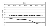
- the inventors of the present application assume that the length of the stretched portion 22a is t and the length of the shielding portion 22b is h, and by lengthening each of these, the distance between the electronic component 11 and the antenna 40 is set. It was confirmed by simulation that the isolation (index value indicating the influence of noise) was reduced.
- 4 and 5 are graphs showing the simulation results of isolation between the electronic component 11 and the antenna 40 when the length t of the stretched portion 22a and the length h of the shielding portion 22b are changed, respectively. .. The length of each part in these graphs is shown in units of the wavelength ⁇ corresponding to the communication frequency of the antenna 40.
- the alternate long and short dash line in these graphs shows the isolation value when the protrusion 22 and the protrusion 32 are not provided.
- the isolation is improved by increasing the lengths t and h, respectively.
- each of the lengths t and h is set to 3 / 10 ⁇ or more, a significant improvement effect is obtained as compared with the case where the protruding portion 22 and the protruding portion 32 are not provided.
- the protruding portion 22 as described above on the front side shield member 20, the side of the main body 21 on the side where the protruding portion 22 is provided (Y-axis positive direction side) is not screwed to the printed circuit board 10. In both cases, noise propagation to the antenna 40 side can be prevented.
- the inventors of the present application have made a difference in isolation between the electronic component 11 and the antenna 40 when the side of the main body 21 on the positive direction side of the Y axis is screwed to the printed circuit board 10 and when it is not screwed. Confirmed by simulation. As a result, it was found that there was almost no deterioration in isolation when screwing was not performed as compared with the case where screwing was performed. That is, in the electronic device 1 according to the present embodiment, by providing the protruding portion 22, it is not necessary to screw the side of the protruding portion 22 side to the printed circuit board 10, and the number of screwed portions can be reduced.
- the antenna is provided from the inside of the front side shield member 20 without screwing the side on the antenna 40 side. It is possible to prevent noise propagation to the 40 side and secure isolation between the electronic component 11 and the antenna 40.
- the embodiments of the present invention are not limited to those described above.
- the protruding portion 22 of the front side shield member 20 may have various shapes having an facing portion facing the side surface of the printed circuit board 10.
- some modifications of the embodiment of the present invention will be described.
- FIG. 6 is a partially enlarged view showing the shapes of the front side shield member 20 and the back side shield member 30 in the electronic device according to the first modification.
- the front side shield member 20 has substantially the same protrusion 22 as compared with the embodiments shown in FIGS. 2 and 3, but the back side shield member 30 includes the protrusion 32.
- the noise propagated from the electronic component 11 is shielded to some extent by the protrusion 22, and the influence of the noise on the antenna 40 can be reduced.
- FIG. 7 is a partially enlarged view showing the shapes of the front side shield member 20 and the back side shield member 30 in the electronic device according to the second modification.
- the back shield member 30 does not include the protrusion 32.
- the protruding portion 22 of the front side shield member 20 is first extended from the main body portion 21 in the positive direction of the Y axis, then bent from there to be extended in the negative direction of the Z axis, and then further bent again and extended in the negative direction of the Y axis. doing.
- the protruding portion 22 has a stretched portion 22a extending in the positive direction of the Y-axis, a shielding portion 22b extending in the negative direction of the Z-axis and facing the side surface of the printed circuit board 10, and a tip portion 22c extending in the negative direction of the Y-axis. And are configured to include.
- the base end of the tip portion 22c is connected to the tip of the shielding portion 22b, and the tip is not connected to other members.
- the tip portion 22c is arranged parallel to the end portion of the back side shield member 30 on the positive direction side of the Y axis, and faces the back side shield member 30 at a predetermined distance.
- FIG. 8 is a partially enlarged view showing the shapes of the front side shield member 20 and the back side shield member 30 in the electronic device according to the third modification.
- the lateral width (width in the X-axis direction) of the protruding portion 22 is substantially the same as that of the main body portion 21, and is formed so as to shield the entire side surface of the printed circuit board 10 on the positive direction side of the Y-axis.
- the lateral width of the protruding portion 22 is shorter than the lateral width of the main body portion 21.
- the lateral width of the protruding portion 32 of the back side shield member 30 is also substantially the same as the lateral width of the protruding portion 22, and is arranged so as to face the protruding portion 22.
- At least the range of the protrusion 22 along the X-axis direction includes the position of the antenna 40 and has a predetermined length range from the antenna 40 in each of the positive and negative directions of the X-axis.
- the protrusion 22 is formed so as to include the above.
- This predetermined length is a length corresponding to the wavelength ⁇ corresponding to the communication frequency of the antenna 40. That is, when the position of the antenna 40 in the X-axis direction is located at the center of the protrusion 22 in the width direction, the width of the protrusion 22 is at least the width w of the antenna 40 in the X-axis direction and the left and right lengths ⁇ . , It is desirable that the total length (w + 2 ⁇ ) or more.
- the side surface of the printed circuit board 10 is opened without being shielded at a portion of the end portion of the main body portion 21 on the positive direction side of the Y-axis where the protruding portion 22 is not provided. Become. By covering this portion with a conductor, the noise shielding effect can be enhanced. Further, the side surface of the waveguide portion G (the surface on the positive direction side and the negative direction side of the X axis) formed by the projecting portion 22 and the projecting portion 32 facing each other is also covered with a conductor to have a noise shielding effect. Can be enhanced.
- 1 electronic device 10 printed circuit board, 11 electronic parts, 20 front side shield member, 21 main body part, 21a convex part, 21b screw, 22 protruding part, 22a extension part, 22b shielding part, 30 back side shield member, 31 main body part, 32 Protruding part, 32a extension part, 32b facing part, 40 antenna.
Abstract
表面に電子部品(11)が搭載されるプリント基板(10)と、プリント基板(10)の表面と対向し、電子部品(11)を覆うように配置されるシールド部材(20)と、を備え、シールド部材(20)は、平面視においてプリント基板(10)の一端を超えて外側に延伸する突出部(22)を有し、突出部(22)は、プリント基板(10)側に曲がっており、その先端が、少なくともプリント基板(10)の側面と対向する位置まで延伸している電子機器(1)である。
Description
本発明は、プリント基板を内蔵する電子機器に関する。
一般に、電子機器は各種の電子部品が搭載されたプリント基板を内蔵している。これらの電子部品の中には、他の電子部品の動作や無線通信などに影響を及ぼすノイズとなる電磁場を発生させるものがある。このようなノイズの伝搬を防止するために、金属板などによって形成されたシールド部材によって、ノイズの発生源となる回路素子を覆うことが行われている。
上述した技術において、シールド部材をプリント基板に完全に密着させることは難しく、シールド部材とプリント基板の間の隙間からノイズが伝搬するおそれがある。
本発明は上記実情を考慮してなされたものであって、その目的の一つは、プリント基板上に配置された回路素子から発生するノイズを、シールド部材によって効果的に抑制することのできる電子機器を提供することにある。
本発明の一態様に係る電子機器は、表面に電子部品が搭載されるプリント基板と、前記プリント基板の表面と対向し、前記電子部品を覆うように配置されるシールド部材と、を備え、前記シールド部材は、平面視において前記プリント基板の一端を超えて外側に延伸する突出部を有し、当該突出部は、前記プリント基板側に曲がっており、その先端が、少なくとも前記プリント基板の側面と対向する位置まで延伸していることを特徴とする。
以下、本発明の実施の形態について、図面に基づき詳細に説明する。
本発明の一実施形態に係る電子機器1は、例えば家庭用ゲーム機等であって、各種の電子部品が搭載されるプリント基板(プリント配線板)10と、プリント基板10に取り付けられる表側シールド部材20、及び裏側シールド部材30と、アンテナ40と、を含んで構成されている。図1は、表側シールド部材20、及び裏側シールド部材30が取り付けられる前の状態のプリント基板10表面の様子を示す斜視図である。図2は、表側シールド部材20、及び裏側シールド部材30が取り付けられた状態のプリント基板10表面の様子を示す斜視図である。また、図3は、表側シールド部材20、及び裏側シールド部材30が取り付けられた状態のプリント基板10を側方から見た位置関係を示す部分断面図である。
プリント基板10の表面には、ノイズの発生源となる少なくとも一つの電子部品11が配置されている。図1ではプリント基板10の表面側に一つの電子部品11のみが示されているが、プリント基板10の表面には複数の電子部品が配置されてよい。また、プリント基板10は両面プリント基板であってよく、裏面側にも1又は複数の電子部品が配置されてよい。
表側シールド部材20及び裏側シールド部材30は、プリント基板10、及びプリント基板10に配置された電子部品から放射されるノイズとなる電磁波を遮蔽するための部材であって、金属板などの導電部材によって形成されている。表側シールド部材20は、プリント基板10の表面と対向するように、かつ、電子部品11を覆うように配置され、プリント基板10に対して固定されている。また、裏側シールド部材30は、プリント基板10の裏面と対向するように配置され、プリント基板10に対して固定されている。これらのシールド部材の構造については、後に詳しく説明する。
アンテナ40は、無線信号を送受信するために用いられる導電体であって、電子機器1はアンテナ40を介して外部の通信機器との間で無線通信を行う。以下では、アンテナ40が無線通信に使用する周波数を通信周波数という。アンテナ40は、プリント基板10から見て所定の方向に離れた位置に配置されている。すなわち、アンテナ40は平面視においてプリント基板10と重ならない位置に配置されている。なお、ここではプリント基板10表面側からプリント基板10表面に垂直な方向を見ることを平面視と表記している。
以下では、プリント基板10から見てアンテナ40が配置されている側を電子機器1の前面側とする。また、以下では説明の便宜のために、プリント基板10表面に平行でプリント基板10とアンテナ40とが並ぶ方向(電子機器1の前後方向)をY軸方向とし、プリント基板10表面に平行でY軸方向と直交する方向(電子機器1の左右方向)をX軸方向とし、プリント基板10の厚さ方向(電子機器1の上下方向)をZ軸方向とする。さらに、電子機器1を正面側から見て向かって右方向をX軸正方向とし、プリント基板10からアンテナ40に向かう側をY軸正方向とし、プリント基板10の裏面から表面に向かう方向をZ軸正方向とする。
本実施形態では、特に電子部品11が、アンテナ40の通信周波数と重複する周波数帯のノイズを放射するものとする。そのため、電子部品11から放射されるノイズがアンテナ40による無線通信を妨げないように、シールド部材によってノイズを遮蔽する必要がある。電子部品11からアンテナ40側に放射されるノイズを遮蔽するために、本実施形態では、表側シールド部材20のアンテナ40側の一端に、プリント基板10の一端からさらに突出する突出部分を設け、この突出部分によってノイズを遮断することとしている。以下、このような作用を実現する表側シールド部材20の構造について説明する。
具体的に表側シールド部材20は、平面視においてプリント基板10と重なる矩形形状を有しており、そのY軸正方向側(アンテナ40側)の一端には、プリント基板10の一端を超えて突出する部分が設けられている。以下では、表側シールド部材20のうち、平面視においてプリント基板10と重なる部分を本体部21とし、本体部21からY軸正方向側に突出した部分を突出部22という。
本体部21は、Z軸正方向側に凸状、負方向側に凹状に形成された凸部21aを備え、この凸部21aが電子部品11を覆っている。また、表側シールド部材20は、本体部21の外周に沿って、複数の位置でねじ21bによってプリント基板10に締結されている。なお、後に詳しく説明するように、本体部21は、Y軸正方向側(アンテナ40側)の一辺を除く3辺に沿ってプリント基板10に対してねじ止めされている。
突出部22は、平面視においてプリント基板10とアンテナ40との間の位置までY軸正方向に延伸しており、その先端部分がZ軸負方向(プリント基板10側)に曲げられた形状を有している。すなわち、突出部22は、プリント基板10表面と略平行にY軸正方向に延伸する延伸部分22aと、プリント基板10表面に対して略直交してZ軸負方向に延伸する遮蔽部分22bと、を含んで構成されている。そして、遮蔽部分22bの上端は延伸部分22aの先端と連結されており、これにより突出部22は全体としてその先端がプリント基板10側に屈曲し、側面(X軸方向)から見てL字形状を有している。
遮蔽部分22bは、電子機器1正面側から見て、少なくともプリント基板10の側面と重なる位置まで延伸している。これにより、遮蔽部分22bは、その一部がプリント基板10のY軸正方向側の側面と対向することになる。遮蔽部分22bの先端部分は、プリント基板10や裏側シールド部材30には接触していない。しかしながら、遮蔽部分22bが少なくともプリント基板10の側面と対向する位置まで延伸することによって、表側シールド部材20はプリント基板10とアンテナ40とを隔てる隔壁として機能し、電子部品11から放射されるノイズがアンテナ40まで到達しないよう遮蔽することができる。
さらに本実施形態では、裏側シールド部材30も、平面視においてプリント基板10と重なる本体部31と、プリント基板10に対してY軸正方向側に突出する突出部32と、を備えている。そして、裏側シールド部材30の突出部32は、プリント基板10裏面と略平行にY軸正方向に延伸する延伸部分32aと、プリント基板10裏面に対して略直交してZ軸負方向に延伸し、上端が延伸部分32aに連結された先端部分32bと、を含んで構成されている。そして、延伸部分32aは表側シールド部材20の延伸部分22aと、先端部分32bは表側シールド部材20の遮蔽部分22bと、それぞれ平行になるように対向配置されている。このように突出部22と突出部32とが対向することによって、その間にX軸方向から見てL字状の空間が形成される。以下では、このL字状の空間を導波部Gという。この導波部Gが、電子部品11から伝搬するノイズの経路を誘導し、その向きを変化させるガイドとして機能する。すなわち、この導波部Gを伝搬することによって、電子部品11からアンテナ40側に放射されたノイズの向きが、Z軸負方向側に変化させられる。これにより、アンテナ40に対して電子部品11からのノイズが影響しにくくなる。
電子部品11によるアンテナ40への影響を低減するためには、導波部Gの長さをより長くすることが望ましい。具体的に本願発明者らは、延伸部分22aの長さをt、遮蔽部分22bの長さをhとした場合に、これらのそれぞれを長くすることによって、電子部品11とアンテナ40との間のアイソレーション(ノイズの影響を示す指標値)が低減することをシミュレーションによって確認した。図4及び図5は、それぞれ延伸部分22aの長さt、及び遮蔽部分22bの長さhを変化させた場合の電子部品11とアンテナ40との間のアイソレーションのシミュレーション結果を示すグラフである。なお、これらのグラフにおける各部の長さは、アンテナ40の通信周波数に対応する波長λを単位として示されている。また、これらのグラフにおける一点鎖線は、突出部22及び突出部32を設けない場合のアイソレーションの値を示している。これらの図に示されるように、長さt及びhをそれぞれ長くすることで、アイソレーションが改善している。特に、長さt及びhのそれぞれを3/10λ以上とすることで、突出部22及び突出部32を設けない場合と比較して有意な改善効果が得られている。
また、表側シールド部材20に以上説明したような突出部22を設けることによって、本体部21の突出部22が設けられた側(Y軸正方向側)の辺をプリント基板10にねじ止めせずとも、アンテナ40側へのノイズ伝搬を防止できるようになる。本願発明者らは、本体部21のY軸正方向側の辺をプリント基板10にねじ止めした場合とねじ止めしない場合のそれぞれについて、電子部品11とアンテナ40との間のアイソレーションの相違をシミュレーションによって確認した。その結果、ねじ止めを行った場合と比較して、ねじ止めを行わない場合のアイソレーションの悪化はほとんどないことが分かった。すなわち、本実施形態に係る電子機器1は、突出部22を設けることによって突出部22側の辺をプリント基板10にねじ止めする必要がなくなり、ねじ止め箇所を少なくすることができる。
以上説明したように、本実施形態に係る電子機器1によれば、表側シールド部材20に突出部22を設けることによって、アンテナ40側の辺をねじ止めすることなく、表側シールド部材20内部からアンテナ40側へのノイズ伝搬を防止し、電子部品11とアンテナ40との間のアイソレーションを確保することができる。
なお、本発明の実施の形態は以上説明したものに限られない。例えば、表側シールド部材20の突出部22は、プリント基板10の側面と対向する対向部分を有する種々の形状であってよい。以下、本発明の実施の形態のいくつかの変形例について、説明する。
図6は、第1の変形例に係る電子機器における表側シールド部材20及び裏側シールド部材30の形状を示す部分拡大図である。この第1の変形例では、図2及び図3に示した実施形態と比較して、表側シールド部材20は略同等の突出部22を備えているが、裏側シールド部材30が突出部32を備えていない。この場合でも、突出部22によって電子部品11から伝搬されるノイズはある程度遮蔽され、アンテナ40へのノイズの影響を低減することができる。
図7は、第2の変形例に係る電子機器における表側シールド部材20及び裏側シールド部材30の形状を示す部分拡大図である。この第2の変形例では、第1の変形例と同様、裏側シールド部材30が突出部32を備えていない。一方、表側シールド部材20の突出部22は、まず本体部21からY軸正方向に延伸し、そこから屈曲してZ軸負方向に延伸した後、さらにもう一度屈曲してY軸負方向に延伸している。すなわち、突出部22は、Y軸正方向に延伸する延伸部分22aと、Z軸負方向に延伸してプリント基板10の側面に対向する遮蔽部分22bと、Y軸負方向に延伸する先端部分22cと、を含んで構成されている。先端部分22cの基端は遮蔽部分22bの先端に連結されており、先端は他の部材に連結されていない。そして、先端部分22cは、裏側シールド部材30のY軸正方向側の端部と平行に配置されており、所定距離離れて裏側シールド部材30と対向している。これにより、電子部品11から放射されるノイズはプリント基板10の側面を回り込んでプリント基板10裏面側に誘導され、アンテナ40に影響を及ぼしにくくなる。
図8は、第3の変形例に係る電子機器における表側シールド部材20及び裏側シールド部材30の形状を示す部分拡大図である。これまでの例では、突出部22の横幅(X軸方向の幅)は、本体部21と略一致しており、プリント基板10のY軸正方向側の側面全体を遮蔽するように形成されている。しかしながら、この第3の変形例では、突出部22の横幅が本体部21の横幅より短くなっている。さらに、裏側シールド部材30の突出部32の横幅も、突出部22の横幅と略一致しており、突出部22に対向するように配置されている。
この第3の変形例では、少なくとも突出部22のX軸方向に沿った範囲が、アンテナ40の位置を含み、かつ、アンテナ40からX軸正方向及び負方向のそれぞれに所定の長さの範囲を含むように、突出部22が形成されている。この所定の長さは、アンテナ40の通信周波数に対応する波長λに相当する長さである。すなわち、アンテナ40のX軸方向の位置が突出部22の幅方向の中心に位置する場合、突出部22の横幅は、少なくともアンテナ40のX軸方向の幅wと、左右それぞれの長さλと、を合計した長さ(w+2λ)以上であることが望ましい。
なお、第3の変形例では、本体部21のY軸正方向側の端部のうち、突出部22が設けられていない箇所において、プリント基板10の側面が遮蔽されずに開放されることになる。この部分も導電体で覆うことによって、ノイズの遮蔽効果を高めることができる。また、突出部22と突出部32が対向して形成される導波部Gの側面(X軸正方向側及び負方向側の面)についても、同じく導電体で塞ぐことによって、ノイズの遮蔽効果を高めることができる。
1 電子機器、10 プリント基板、11 電子部品、20 表側シールド部材、21 本体部、21a 凸部、21b ねじ、22 突出部、22a 延伸部分、22b 遮蔽部分、30 裏側シールド部材、31 本体部、32 突出部、32a 延伸部分、32b 対向部分、40 アンテナ。
Claims (5)
- 表面に電子部品が搭載されるプリント基板と、
前記プリント基板の表面と対向し、前記電子部品を覆うように配置されるシールド部材と、
を備え、
前記シールド部材は、平面視において前記プリント基板の一端を超えて外側に延伸する突出部を有し、当該突出部は、前記プリント基板側に曲がっており、その先端が、少なくとも前記プリント基板の側面と対向する位置まで延伸している
ことを特徴とする電子機器。 - 請求項1に記載の電子機器において、
前記電子機器は、前記プリント基板の裏面と対向して配置される裏側シールド部材をさらに備え、
前記シールド部材の前記突出部は、その先端が前記プリント基板の側面と対向する位置を超えてさらに延伸し、当該側面と対向する位置を超えて延伸する先端部分は、前記裏側シールド部材と対向している
ことを特徴とする電子機器。 - 請求項2に記載の電子機器において、
前記裏側シールド部材は、平面視において前記プリント基板の前記一端を超えて外側に延伸する突出部を有し、当該突出部は、前記プリント基板から離れる側に曲がっており、その先端部分が、前記シールド部材の前記先端部分と対向している
ことを特徴とする電子機器。 - 請求項2に記載の電子機器において、
前記シールド部材の前記突出部は、前記プリント基板の側面と対向する位置を超えた位置でさらに前記プリント基板に近づく側に曲がっており、当該曲がった部分が、前記裏側シールド部材と対向している
ことを特徴とする電子機器。 - 請求項1から4のいずれか一項に記載の電子機器において、
平面視において前記プリント基板と重ならず、前記プリント基板の前記一端の側に離れた位置にアンテナが配置されており、
前記シールド部材の前記突出部は、前記プリント基板の前記一端と前記アンテナの間の位置で、前記プリント基板側に曲がっている
ことを特徴とする電子機器。
Priority Applications (2)
| Application Number | Priority Date | Filing Date | Title |
|---|---|---|---|
| JP2021528107A JPWO2020255790A1 (ja) | 2019-06-17 | 2020-06-09 | |
| US17/616,319 US20220322584A1 (en) | 2019-06-17 | 2020-06-09 | Electronic device |
Applications Claiming Priority (2)
| Application Number | Priority Date | Filing Date | Title |
|---|---|---|---|
| JP2019-112277 | 2019-06-17 | ||
| JP2019112277 | 2019-06-17 |
Publications (1)
| Publication Number | Publication Date |
|---|---|
| WO2020255790A1 true WO2020255790A1 (ja) | 2020-12-24 |
Family
ID=74037248
Family Applications (1)
| Application Number | Title | Priority Date | Filing Date |
|---|---|---|---|
| PCT/JP2020/022661 WO2020255790A1 (ja) | 2019-06-17 | 2020-06-09 | 電子機器 |
Country Status (3)
| Country | Link |
|---|---|
| US (1) | US20220322584A1 (ja) |
| JP (1) | JPWO2020255790A1 (ja) |
| WO (1) | WO2020255790A1 (ja) |
Citations (6)
| Publication number | Priority date | Publication date | Assignee | Title |
|---|---|---|---|---|
| JPS59112973U (ja) * | 1983-01-20 | 1984-07-30 | 富士通株式会社 | 高周波用混成集積回路のケ−ス格納構造 |
| US5557064A (en) * | 1994-04-18 | 1996-09-17 | Motorola, Inc. | Conformal shield and method for forming same |
| JPH10229289A (ja) * | 1997-02-24 | 1998-08-25 | Sega Enterp Ltd | ノイズシールド構造を備える電子機器 |
| JP2002344172A (ja) * | 2001-05-16 | 2002-11-29 | Matsushita Electric Ind Co Ltd | 無線端末装置 |
| JP2008005461A (ja) * | 2006-05-24 | 2008-01-10 | Sharp Corp | 衛星信号用コンバータ、アンテナ装置および衛星放送受信装置 |
| JP2018060991A (ja) * | 2016-09-28 | 2018-04-12 | 住友ベークライト株式会社 | 封止用フィルム、電子部品搭載基板の封止方法および封止用フィルム被覆電子部品搭載基板 |
Family Cites Families (13)
| Publication number | Priority date | Publication date | Assignee | Title |
|---|---|---|---|---|
| US4910434A (en) * | 1988-03-31 | 1990-03-20 | Digital Equipment Corporation | Multifunctional enclosure for wiring board in display |
| US5436803A (en) * | 1993-12-16 | 1995-07-25 | Schlegel Corporation | Emi shielding having flexible conductive envelope |
| US6134121A (en) * | 1998-02-02 | 2000-10-17 | Motorola, Inc. | Housing assembly utilizing a heat shrinkable composite laminate |
| US6137051A (en) * | 1998-12-09 | 2000-10-24 | Nortel Networks Corporation | EMI shield/ gasket enclosure |
| US6900383B2 (en) * | 2001-03-19 | 2005-05-31 | Hewlett-Packard Development Company, L.P. | Board-level EMI shield that adheres to and conforms with printed circuit board component and board surfaces |
| DE10260459A1 (de) * | 2002-01-08 | 2003-08-14 | Mitsumi Electric Co Ltd | Abschirmummantelung für elektronische Geräte |
| JP4096605B2 (ja) * | 2002-04-23 | 2008-06-04 | 日本電気株式会社 | 半導体装置および半導体装置のシールド形成方法 |
| US8634823B2 (en) * | 2010-06-01 | 2014-01-21 | Hendrikus A. Le Sage | Retrofit inline antenna power monitor system and method |
| CN104221295B (zh) * | 2012-04-03 | 2016-01-20 | 三菱电机株式会社 | Emc屏蔽装置 |
| TW201511655A (zh) * | 2013-09-05 | 2015-03-16 | Hon Hai Prec Ind Co Ltd | 電子裝置 |
| EP3352548B1 (en) * | 2015-09-18 | 2020-10-28 | Toray Industries, Inc. | Electronic device housing |
| US10652996B2 (en) * | 2015-12-21 | 2020-05-12 | 3M Innovative Properties Company | Formable shielding film |
| US20190391052A1 (en) * | 2017-01-18 | 2019-12-26 | Kevin Hart | Duct mounted air quality monitoring system, method and device |
-
2020
- 2020-06-09 JP JP2021528107A patent/JPWO2020255790A1/ja active Pending
- 2020-06-09 WO PCT/JP2020/022661 patent/WO2020255790A1/ja active Application Filing
- 2020-06-09 US US17/616,319 patent/US20220322584A1/en active Pending
Patent Citations (6)
| Publication number | Priority date | Publication date | Assignee | Title |
|---|---|---|---|---|
| JPS59112973U (ja) * | 1983-01-20 | 1984-07-30 | 富士通株式会社 | 高周波用混成集積回路のケ−ス格納構造 |
| US5557064A (en) * | 1994-04-18 | 1996-09-17 | Motorola, Inc. | Conformal shield and method for forming same |
| JPH10229289A (ja) * | 1997-02-24 | 1998-08-25 | Sega Enterp Ltd | ノイズシールド構造を備える電子機器 |
| JP2002344172A (ja) * | 2001-05-16 | 2002-11-29 | Matsushita Electric Ind Co Ltd | 無線端末装置 |
| JP2008005461A (ja) * | 2006-05-24 | 2008-01-10 | Sharp Corp | 衛星信号用コンバータ、アンテナ装置および衛星放送受信装置 |
| JP2018060991A (ja) * | 2016-09-28 | 2018-04-12 | 住友ベークライト株式会社 | 封止用フィルム、電子部品搭載基板の封止方法および封止用フィルム被覆電子部品搭載基板 |
Also Published As
| Publication number | Publication date |
|---|---|
| US20220322584A1 (en) | 2022-10-06 |
| JPWO2020255790A1 (ja) | 2020-12-24 |
Similar Documents
| Publication | Publication Date | Title |
|---|---|---|
| TWI672092B (zh) | 電子裝置及電磁干擾抑制體的配置方法、與通信裝置 | |
| US7703994B2 (en) | Optical transceiver module | |
| US9042722B2 (en) | Optical transceiver having enhanced EMI tolerance | |
| JP6012220B2 (ja) | 高周波シールド構造 | |
| US20130027255A1 (en) | Radio apparatus | |
| KR20070057278A (ko) | 실드가 부착된 커넥터 및 회로 기판 장치 | |
| JP2021196476A (ja) | 光モジュール | |
| US20120024587A1 (en) | Radiation amount reducing device | |
| US20200084879A1 (en) | Electronic device | |
| WO2020255790A1 (ja) | 電子機器 | |
| JP4498305B2 (ja) | シールド筐体 | |
| WO2018128120A1 (ja) | 電子機器 | |
| US8149593B2 (en) | Radiation level reducing device | |
| JP7278233B2 (ja) | 電子機器 | |
| JP7083400B2 (ja) | 電子機器 | |
| JP2006210742A (ja) | 電子機器用シールドケースおよび電子機器 | |
| JP7382750B2 (ja) | 電子回路モジュール | |
| JP5981466B2 (ja) | 平面伝送線路導波管変換器 | |
| WO2022215713A1 (ja) | アンテナ装置 | |
| JP6861904B1 (ja) | 電磁シールドケース | |
| US10863615B2 (en) | Electronic apparatus | |
| JP6138410B2 (ja) | 高周波モジュール | |
| JP6688719B2 (ja) | 電子制御ユニット | |
| WO2017169545A1 (ja) | 高周波モジュール | |
| GB2601333A (en) | Electromagnetic interference shield device |
Legal Events
| Date | Code | Title | Description |
|---|---|---|---|
| 121 | Ep: the epo has been informed by wipo that ep was designated in this application |
Ref document number: 20827485 Country of ref document: EP Kind code of ref document: A1 |
|
| ENP | Entry into the national phase |
Ref document number: 2021528107 Country of ref document: JP Kind code of ref document: A |
|
| NENP | Non-entry into the national phase |
Ref country code: DE |
|
| 122 | Ep: pct application non-entry in european phase |
Ref document number: 20827485 Country of ref document: EP Kind code of ref document: A1 |