WO2020235597A1 - 半導体装置を製造する方法 - Google Patents
半導体装置を製造する方法 Download PDFInfo
- Publication number
- WO2020235597A1 WO2020235597A1 PCT/JP2020/019963 JP2020019963W WO2020235597A1 WO 2020235597 A1 WO2020235597 A1 WO 2020235597A1 JP 2020019963 W JP2020019963 W JP 2020019963W WO 2020235597 A1 WO2020235597 A1 WO 2020235597A1
- Authority
- WO
- WIPO (PCT)
- Prior art keywords
- light
- layer
- curable resin
- support substrate
- meth
- Prior art date
- Legal status (The legal status is an assumption and is not a legal conclusion. Google has not performed a legal analysis and makes no representation as to the accuracy of the status listed.)
- Ceased
Links
Images


Classifications
-
- C—CHEMISTRY; METALLURGY
- C09—DYES; PAINTS; POLISHES; NATURAL RESINS; ADHESIVES; COMPOSITIONS NOT OTHERWISE PROVIDED FOR; APPLICATIONS OF MATERIALS NOT OTHERWISE PROVIDED FOR
- C09J—ADHESIVES; NON-MECHANICAL ASPECTS OF ADHESIVE PROCESSES IN GENERAL; ADHESIVE PROCESSES NOT PROVIDED FOR ELSEWHERE; USE OF MATERIALS AS ADHESIVES
- C09J5/00—Adhesive processes in general; Adhesive processes not provided for elsewhere, e.g. relating to primers
-
- H—ELECTRICITY
- H10—SEMICONDUCTOR DEVICES; ELECTRIC SOLID-STATE DEVICES NOT OTHERWISE PROVIDED FOR
- H10W—GENERIC PACKAGES, INTERCONNECTIONS, CONNECTORS OR OTHER CONSTRUCTIONAL DETAILS OF DEVICES COVERED BY CLASS H10
- H10W74/00—Encapsulations, e.g. protective coatings
- H10W74/01—Manufacture or treatment
- H10W74/019—Manufacture or treatment using temporary auxiliary substrates
-
- H—ELECTRICITY
- H10—SEMICONDUCTOR DEVICES; ELECTRIC SOLID-STATE DEVICES NOT OTHERWISE PROVIDED FOR
- H10P—GENERIC PROCESSES OR APPARATUS FOR THE MANUFACTURE OR TREATMENT OF DEVICES COVERED BY CLASS H10
- H10P14/00—Formation of materials, e.g. in the shape of layers or pillars
- H10P14/60—Formation of materials, e.g. in the shape of layers or pillars of insulating materials
- H10P14/65—Formation of materials, e.g. in the shape of layers or pillars of insulating materials characterised by treatments performed before or after the formation of the materials
- H10P14/6516—Formation of materials, e.g. in the shape of layers or pillars of insulating materials characterised by treatments performed before or after the formation of the materials of treatments performed after formation of the materials
- H10P14/6528—In-situ cleaning after layer formation, e.g. removing process residues
-
- H—ELECTRICITY
- H10—SEMICONDUCTOR DEVICES; ELECTRIC SOLID-STATE DEVICES NOT OTHERWISE PROVIDED FOR
- H10P—GENERIC PROCESSES OR APPARATUS FOR THE MANUFACTURE OR TREATMENT OF DEVICES COVERED BY CLASS H10
- H10P14/00—Formation of materials, e.g. in the shape of layers or pillars
- H10P14/60—Formation of materials, e.g. in the shape of layers or pillars of insulating materials
- H10P14/65—Formation of materials, e.g. in the shape of layers or pillars of insulating materials characterised by treatments performed before or after the formation of the materials
- H10P14/6516—Formation of materials, e.g. in the shape of layers or pillars of insulating materials characterised by treatments performed before or after the formation of the materials of treatments performed after formation of the materials
- H10P14/6536—Formation of materials, e.g. in the shape of layers or pillars of insulating materials characterised by treatments performed before or after the formation of the materials of treatments performed after formation of the materials by exposure to radiation, e.g. visible light
-
- H—ELECTRICITY
- H10—SEMICONDUCTOR DEVICES; ELECTRIC SOLID-STATE DEVICES NOT OTHERWISE PROVIDED FOR
- H10P—GENERIC PROCESSES OR APPARATUS FOR THE MANUFACTURE OR TREATMENT OF DEVICES COVERED BY CLASS H10
- H10P54/00—Cutting or separating of wafers, substrates or parts of devices
-
- H—ELECTRICITY
- H10—SEMICONDUCTOR DEVICES; ELECTRIC SOLID-STATE DEVICES NOT OTHERWISE PROVIDED FOR
- H10P—GENERIC PROCESSES OR APPARATUS FOR THE MANUFACTURE OR TREATMENT OF DEVICES COVERED BY CLASS H10
- H10P72/00—Handling or holding of wafers, substrates or devices during manufacture or treatment thereof
- H10P72/70—Handling or holding of wafers, substrates or devices during manufacture or treatment thereof for supporting or gripping
- H10P72/74—Handling or holding of wafers, substrates or devices during manufacture or treatment thereof for supporting or gripping using temporarily an auxiliary support
- H10P72/7412—Handling or holding of wafers, substrates or devices during manufacture or treatment thereof for supporting or gripping using temporarily an auxiliary support the auxiliary support including means facilitating the separation of a device or wafer from the auxiliary support
-
- H—ELECTRICITY
- H10—SEMICONDUCTOR DEVICES; ELECTRIC SOLID-STATE DEVICES NOT OTHERWISE PROVIDED FOR
- H10W—GENERIC PACKAGES, INTERCONNECTIONS, CONNECTORS OR OTHER CONSTRUCTIONAL DETAILS OF DEVICES COVERED BY CLASS H10
- H10W74/00—Encapsulations, e.g. protective coatings
- H10W74/01—Manufacture or treatment
- H10W74/014—Manufacture or treatment using batch processing
-
- C—CHEMISTRY; METALLURGY
- C09—DYES; PAINTS; POLISHES; NATURAL RESINS; ADHESIVES; COMPOSITIONS NOT OTHERWISE PROVIDED FOR; APPLICATIONS OF MATERIALS NOT OTHERWISE PROVIDED FOR
- C09J—ADHESIVES; NON-MECHANICAL ASPECTS OF ADHESIVE PROCESSES IN GENERAL; ADHESIVE PROCESSES NOT PROVIDED FOR ELSEWHERE; USE OF MATERIALS AS ADHESIVES
- C09J2203/00—Applications of adhesives in processes or use of adhesives in the form of films or foils
- C09J2203/326—Applications of adhesives in processes or use of adhesives in the form of films or foils for bonding electronic components such as wafers, chips or semiconductors
-
- C—CHEMISTRY; METALLURGY
- C09—DYES; PAINTS; POLISHES; NATURAL RESINS; ADHESIVES; COMPOSITIONS NOT OTHERWISE PROVIDED FOR; APPLICATIONS OF MATERIALS NOT OTHERWISE PROVIDED FOR
- C09J—ADHESIVES; NON-MECHANICAL ASPECTS OF ADHESIVE PROCESSES IN GENERAL; ADHESIVE PROCESSES NOT PROVIDED FOR ELSEWHERE; USE OF MATERIALS AS ADHESIVES
- C09J2301/00—Additional features of adhesives in the form of films or foils
- C09J2301/40—Additional features of adhesives in the form of films or foils characterized by the presence of essential components
- C09J2301/416—Additional features of adhesives in the form of films or foils characterized by the presence of essential components use of irradiation
-
- C—CHEMISTRY; METALLURGY
- C09—DYES; PAINTS; POLISHES; NATURAL RESINS; ADHESIVES; COMPOSITIONS NOT OTHERWISE PROVIDED FOR; APPLICATIONS OF MATERIALS NOT OTHERWISE PROVIDED FOR
- C09J—ADHESIVES; NON-MECHANICAL ASPECTS OF ADHESIVE PROCESSES IN GENERAL; ADHESIVE PROCESSES NOT PROVIDED FOR ELSEWHERE; USE OF MATERIALS AS ADHESIVES
- C09J2301/00—Additional features of adhesives in the form of films or foils
- C09J2301/50—Additional features of adhesives in the form of films or foils characterized by process specific features
- C09J2301/502—Additional features of adhesives in the form of films or foils characterized by process specific features process for debonding adherents
-
- C—CHEMISTRY; METALLURGY
- C09—DYES; PAINTS; POLISHES; NATURAL RESINS; ADHESIVES; COMPOSITIONS NOT OTHERWISE PROVIDED FOR; APPLICATIONS OF MATERIALS NOT OTHERWISE PROVIDED FOR
- C09J—ADHESIVES; NON-MECHANICAL ASPECTS OF ADHESIVE PROCESSES IN GENERAL; ADHESIVE PROCESSES NOT PROVIDED FOR ELSEWHERE; USE OF MATERIALS AS ADHESIVES
- C09J7/00—Adhesives in the form of films or foils
- C09J7/30—Adhesives in the form of films or foils characterised by the adhesive composition
- C09J7/35—Heat-activated
-
- H—ELECTRICITY
- H10—SEMICONDUCTOR DEVICES; ELECTRIC SOLID-STATE DEVICES NOT OTHERWISE PROVIDED FOR
- H10P—GENERIC PROCESSES OR APPARATUS FOR THE MANUFACTURE OR TREATMENT OF DEVICES COVERED BY CLASS H10
- H10P72/00—Handling or holding of wafers, substrates or devices during manufacture or treatment thereof
- H10P72/70—Handling or holding of wafers, substrates or devices during manufacture or treatment thereof for supporting or gripping
- H10P72/74—Handling or holding of wafers, substrates or devices during manufacture or treatment thereof for supporting or gripping using temporarily an auxiliary support
- H10P72/7416—Handling or holding of wafers, substrates or devices during manufacture or treatment thereof for supporting or gripping using temporarily an auxiliary support used during dicing or grinding
-
- H—ELECTRICITY
- H10—SEMICONDUCTOR DEVICES; ELECTRIC SOLID-STATE DEVICES NOT OTHERWISE PROVIDED FOR
- H10P—GENERIC PROCESSES OR APPARATUS FOR THE MANUFACTURE OR TREATMENT OF DEVICES COVERED BY CLASS H10
- H10P72/00—Handling or holding of wafers, substrates or devices during manufacture or treatment thereof
- H10P72/70—Handling or holding of wafers, substrates or devices during manufacture or treatment thereof for supporting or gripping
- H10P72/74—Handling or holding of wafers, substrates or devices during manufacture or treatment thereof for supporting or gripping using temporarily an auxiliary support
- H10P72/7428—Handling or holding of wafers, substrates or devices during manufacture or treatment thereof for supporting or gripping using temporarily an auxiliary support used to support diced chips prior to mounting
-
- H—ELECTRICITY
- H10—SEMICONDUCTOR DEVICES; ELECTRIC SOLID-STATE DEVICES NOT OTHERWISE PROVIDED FOR
- H10P—GENERIC PROCESSES OR APPARATUS FOR THE MANUFACTURE OR TREATMENT OF DEVICES COVERED BY CLASS H10
- H10P72/00—Handling or holding of wafers, substrates or devices during manufacture or treatment thereof
- H10P72/70—Handling or holding of wafers, substrates or devices during manufacture or treatment thereof for supporting or gripping
- H10P72/74—Handling or holding of wafers, substrates or devices during manufacture or treatment thereof for supporting or gripping using temporarily an auxiliary support
- H10P72/744—Details of chemical or physical process used for separating the auxiliary support from a device or a wafer
- H10P72/7442—Separation by peeling
-
- H—ELECTRICITY
- H10—SEMICONDUCTOR DEVICES; ELECTRIC SOLID-STATE DEVICES NOT OTHERWISE PROVIDED FOR
- H10W—GENERIC PACKAGES, INTERCONNECTIONS, CONNECTORS OR OTHER CONSTRUCTIONAL DETAILS OF DEVICES COVERED BY CLASS H10
- H10W72/00—Interconnections or connectors in packages
- H10W72/01—Manufacture or treatment
- H10W72/0198—Manufacture or treatment batch processes
Definitions
- the present invention relates to a method for manufacturing a semiconductor device.
- Patent Documents 1 to 3 disclose a method of separating a semiconductor member by irradiating a temporary fixing material layer with laser light (coherent light).
- One aspect of the present invention provides a method for manufacturing a semiconductor device, which includes a step of processing a semiconductor member temporarily fixed to a support substrate, so that the processed semiconductor member can be easily separated from the support substrate. To do.
- a temporary fixing laminate including a support substrate having a support surface and a back surface on the opposite side thereof and a temporary fixing material layer provided on the support surface, wherein the temporary fixing material layer is the temporary fixing material layer.
- a method for manufacturing a semiconductor device which is provided in this order.
- a part or all of the temporary fixing material layer is a light absorbing layer that absorbs light and generates heat.
- the light is sequentially applied to a plurality of irradiated areas, and each irradiated area includes a part of the back surface.
- the adjacent irradiated regions When viewed from a direction perpendicular to the back surface, the adjacent irradiated regions partially overlap each other, and the combined region of the plurality of irradiated regions includes the entire back surface.
- the processed semiconductor member can be easily processed from the support substrate by a simple process.
- a method that can be separated is provided.
- (A), (b) and (c) are schematic diagrams showing an embodiment of a method for manufacturing a semiconductor device.
- (A) and (b) are schematic diagrams showing an embodiment of a method for manufacturing a semiconductor device.
- (A) and (b) are schematic diagrams showing an embodiment of a method for manufacturing a semiconductor device.
- (A), (b) and (c) are schematic diagrams showing an embodiment of a method for manufacturing a semiconductor device. It is a top view which shows an example of a plurality of irradiated areas. It is a top view which shows an example of a plurality of irradiated areas. It is a top view which shows an example of a plurality of irradiated areas. It is a top view which shows an example of a plurality of irradiated areas. It is a top view which shows an example of a plurality of irradiated areas. It is a top view which shows an example of a plurality of irradiated areas.
- the numerical values and their ranges in the present specification also do not limit the scope of the present invention.
- the numerical range indicated by using "-" indicates a range including the numerical values before and after "-" as the minimum value and the maximum value, respectively.
- the upper limit value or the lower limit value described in one numerical range may be replaced with the upper limit value or the lower limit value of another numerical range described stepwise. Good.
- the upper limit value or the lower limit value of the numerical range may be replaced with the value shown in the examples.
- (meth) acrylic acid means acrylic acid or methacrylic acid corresponding thereto.
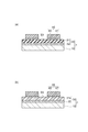
- FIG. 1 is a cross-sectional view showing some embodiments of a temporary fixing laminate.
- the temporary fixing laminate 1 shown in FIG. 1 has a support substrate 10 having a main surface as a support surface S1 and a back surface S2 on the back side thereof, and a temporary fixing material layer 30 provided on the support surface S1 of the support substrate 10. And have.
- the temporary fixing material layer 30 has a curable resin layer 31.
- the curable resin layer 31 includes the outermost surface S3 on the side of the temporary fixing material layer 30 opposite to the support substrate 10.
- the temporary fixing material layer 30 has a light absorption layer 32 provided as a layer separate from the curable resin layer 31, or a light absorption layer 31B provided as a part of the curable resin layer 31.
- the light absorption layers 32 and 31B are layers that absorb light and generate heat.
- the temporary fixing material layer 30 of the temporary fixing laminate 1 shown in FIG. 1A is a curable resin layer 31 including the outermost surface S3 on the opposite side of the support substrate 10, and the curable resin layer 31. It has a light absorbing layer 32 provided as another layer. In other words, the light absorption layer 32 and the curable resin layer 31 are laminated in this order on the support surface S1 which is one main surface of the support substrate 10.
- the temporary fixing material layer 30 of the temporary fixing laminate 1 shown in FIG. 1B is composed of a curable resin layer 31 including a light absorption layer 31B as a part thereof.
- the curable resin layer 31 here has a light absorbing layer 31B including the outermost surface S3, and a substantially non-thermosetting curable resin layer 31A provided on the support substrate 10 side of the light absorbing layer 31B. ..
- the light absorbing layer 32 is a curable resin layer 31. It is further provided as a separate layer from the above. Instead of the light absorbing layer 32 provided as a layer separate from the curable resin layer 31, the light absorbing layer forming a part of the curable resin layer 31 is placed between the curable resin layer 31A and the support substrate 10. Further may be provided.
- the temporary fixing laminate 1 can be obtained, for example, by sequentially forming each layer on the support substrate 10.
- a laminated film having a curable resin layer and a light absorbing layer may be prepared and laminated on the support substrate 10.
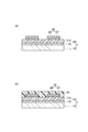
- FIGS. 2 to 4 are process diagrams showing an embodiment of a method of manufacturing a semiconductor device using a temporary fixing laminate.
- the method using the temporary fixing laminate 1 of FIG. 1A is exemplified, but a semiconductor device can be similarly manufactured by using the temporary fixing laminate 1 having another configuration.
- the methods shown in FIGS. 2 to 4 include a step of temporarily fixing the semiconductor member 45 to the support substrate 10 via the temporary fixing material layer 30 (FIG. 2) and a semiconductor member temporarily fixed to the support substrate 10.
- the step of processing the 45 FIG. 3 (a)
- the step of forming the sealing layer 50 for sealing the processed semiconductor member 45 (FIG. 3 (b)
- a step of irradiating light h ⁇ from the support substrate 10 side and thereby separating the semiconductor member 45 from the support substrate 10 (FIG. 4B) is provided in this order.
- the semiconductor member 45 has a rewiring layer 41 provided on one surface side of the semiconductor substrate 40 and the semiconductor substrate 40.
- the semiconductor member 45 may be arranged on the curable resin layer 31 with the rewiring layer 41 facing the curable resin layer 31 side.
- the support substrate 10 is a plate-like body having a high transmittance and capable of withstanding a load received during processing of the semiconductor member 45.
- Examples of the support substrate 10 include an inorganic glass substrate and a transparent resin substrate.
- the thickness of the support substrate 10 may be, for example, 0.1 to 2.0 mm. When the thickness of the support substrate 10 is 0.1 mm or more, handling tends to be easy. When the thickness of the support substrate 10 is 2.0 mm or less, the material cost tends to be suppressed.
- the outermost surface S3 on the side where the semiconductor member 45 of the temporary fixing material layer 30 is temporarily fixed is the surface of the curable resin layer 31.
- the semiconductor member 45 can be temporarily fixed to the support substrate 10 by curing the curable resin layer 31 with the semiconductor member 45 mounted on the curable resin layer 31.
- the semiconductor member 45 can be temporarily adhered to the support substrate 10 via the temporary fixing material layer 30 having the cured curable resin layer 31c.
- the curable resin layer 31 is a layer containing a curable resin composition that is cured by heat or light.
- the curable resin layer 31 before curing has adhesiveness (or stickability) to such an extent that the semiconductor member 45 can be stuck by pressure bonding or the like.
- the cured curable resin layer 31c holds the semiconductor member 45 to be processed.
- all the components other than the conductive particles constituting the curable resin layer 31 are regarded as the components of the curable resin composition.
- the thickness of the curable resin layer 31 may be, for example, 2000 ⁇ m or less, 500 ⁇ m or less, or 200 ⁇ m or less, 0.1 ⁇ m or more, or 1 ⁇ m or more.
- the storage elastic modulus of the cured curable resin layer 31c at 25 ° C. may be 5 to 100 MPa.
- the storage elastic modulus of the cured curable resin layer 31c at 25 ° C. is 5 MPa or more, the support substrate 10 does not bend and the semiconductor member 45 can be easily held. Further, when the semiconductor member 45 is separated from the support substrate, the curable resin layer 31c tends to be difficult to leave a residue on the semiconductor member 45.
- the storage elastic modulus of the cured curable resin layer 31c at 25 ° C. is 100 MPa or less, the displacement of the semiconductor member 45 tends to be small. From the same viewpoint, the storage elastic modulus of the cured curable resin layer 31c at 25 ° C.
- the storage elastic modulus of the cured curable resin layer 31c means a value obtained by viscoelasticity measurement measured under the conditions of a heating rate of 5 ° C./min, a frequency of 1 Hz, and a tensile mode.
- the storage elastic modulus of the cured curable resin layer 31c at 25 ° C. is, for example, a hydrocarbon resin composition having an insulating filler, which increases the content of the hydrocarbon resin described below, applies a hydrocarbon resin having a high Tg. It can be increased by a method such as adding to.
- the storage elastic modulus of the cured curable resin layer 31c at 250 ° C. may be 0.70 MPa or more, 0.80 MPa or more, 0.85 MPa or more, or 0.90 MPa or more, and 2.00 MPa or less, 1.90 MPa or less. Hereinafter, it may be 1.80 MPa or less, or 1.75 MPa or less.
- the curable resin composition constituting the curable resin layer 31 may contain a thermosetting resin and a hydrocarbon resin.
- a hydrocarbon resin is a resin whose main skeleton is composed of hydrocarbons.
- the glass transition temperature (Tg) of the hydrocarbon resin may be 50 ° C. or lower. From the viewpoint of good peelability of the curable resin layer 31, the Tg of the hydrocarbon resin may be ⁇ 100 ° C. or higher, or ⁇ 50 ° C. or higher.
- the Tg of the hydrocarbon resin is the intermediate point glass transition temperature value obtained by differential scanning calorimetry (DSC). Specifically, the Tg of the hydrocarbon resin is an intermediate point glass calculated by a method based on JIS K7121 by measuring the change in calorific value under the conditions of a temperature rising rate of 10 ° C./min and a measurement temperature of -80 to 80 ° C. The transition temperature.
- the hydrocarbon resin includes, for example, ethylene / styrene copolymer, ethylene / 1-butene copolymer, ethylene / propylene / 1-butene copolymer elastomer, ethylene / 1-hexene copolymer, and ethylene / 1-octene.
- hydrocarbon resins may have a carboxyl group.
- the carboxyl group is introduced by, for example, modification with maleic anhydride or the like.
- the hydrocarbon resin may contain a styrene-based resin containing a monomer unit derived from styrene.
- the styrene resin may be a styrene / ethylene / butylene / styrene block copolymer (SEBS).
- the weight average molecular weight (Mw) of the hydrocarbon resin may be 10,000 to 5 million or 100,000 to 2 million.
- Mw weight average molecular weight
- the weight average molecular weight here is a polystyrene-equivalent value using a calibration curve using standard polystyrene by gel permeation chromatography (GPC).
- the content of the hydrocarbon resin may be 40 parts by mass or more, 50 parts by mass or more, or 60 parts by mass or more with respect to 100 parts by mass of the total mass of the curable resin composition constituting the curable resin layer 31. , 90 parts by mass or less, 85 parts by mass or less, or 80 parts by mass or less.
- the content of the hydrocarbon resin is within these numerical values, the thin and flat curable resin layer 31 tends to be easily formed. Further, the curable resin layer 31 tends to have good pressure-sensitive adhesiveness at low temperature and an appropriate storage elastic modulus after curing.
- the thermosetting resin is a component that cures the curable resin composition by a thermosetting reaction.
- the thermosetting reaction can be a reaction between a thermosetting resin and a curing agent, self-polymerization of a thermosetting resin, or a combination thereof.
- the thermosetting resin include epoxy resin, acrylic resin, silicone resin, phenol resin, thermosetting polyimide resin, polyurethane resin, melamine resin, and urea resin. These may be used individually by 1 type or in combination of 2 or more type.
- the thermosetting resin may contain an epoxy resin because it is excellent in heat resistance, workability, and reliability.
- Epoxy resin is a compound having one or more epoxy groups.
- the epoxy resin may have two or more epoxy groups.
- Examples of epoxy resins having two or more epoxy groups include bisphenol A type epoxy resin, novolac type epoxy resin (phenol novolac type epoxy resin, etc.), glycidylamine type epoxy resin, heterocycle-containing epoxy resin, and alicyclic epoxy. Resin is mentioned.
- the curable resin composition may contain a thermosetting resin and a curing agent thereof.
- the total content of the thermosetting resin and the curing agent thereof may be 10 parts by mass or more, 15 parts by mass or more, or 20 parts by mass or more with respect to 100 parts by mass of the total mass of the curable resin composition. It may be 60 parts by mass or less, 50 parts by mass or less, or 40 parts by mass or less.
- the total content of the thermosetting resin and its curing agent is within these ranges, the thin and flat curable resin layer tends to be easily formed, and the heat resistance of the cured curable resin layer 31c is more excellent. Tend.
- the curable resin composition may contain a curing agent for the epoxy resin.
- the curing agent for the epoxy resin is not particularly limited, and examples thereof include amine, polyamide, acid anhydride, polysulfide, boron trifluoride, bisphenol (bisphenol A, bisphenol F, bisphenol S, etc.), and phenol resin (phenol).
- the thermosetting resin composition may further contain a curing accelerator that accelerates the curing reaction of the thermosetting resin such as epoxy resin.
- curing accelerators include imidazole compounds, dicyandiamide, dicarboxylic acid dihydrazide, triphenylphosphine, tetraphenylphosphonium tetraphenylborate, 2-ethyl-4-methylimidazole-tetraphenylborate, and 1,8-diazabicyclo [5, 4,0] Undecene-7-tetraphenylborate can be mentioned. These may be used individually by 1 type or in combination of 2 or more type.
- the content of the curing accelerator may be 0.01 to 5 parts by mass with respect to 100 parts by mass of the total amount of the thermosetting resin and the curing agent. When the content of the curing accelerator is within this range, the curability of the curable resin layer and the heat resistance after curing tend to be more excellent.
- the curable resin composition constituting the curable resin layer 31 may contain a polymerizable monomer having a polymerizable unsaturated group and a polymerization initiator. In this case as well, the curable resin composition may further contain the above-mentioned hydrocarbon resin.
- the polymerizable monomer is a compound having a polymerizable unsaturated group such as an ethylenically unsaturated group.
- the polymerizable monomer may be monofunctional, bifunctional, or trifunctional or higher, but a bifunctional or higher polymerizable monomer may be used from the viewpoint of obtaining sufficient curability.
- Examples of the polymerizable monomer include (meth) acrylate, vinylidene halide, vinyl ether, vinyl ester, vinylpyridine, vinylamide, and vinyl arylated.
- the polymerizable monomer may be (meth) acrylate or (meth) acrylic acid.
- the (meth) acrylate may be a monofunctional (meth) acrylate, a bifunctional (meth) acrylate, a trifunctional or higher polyfunctional (meth) acrylate, or a combination thereof.
- Examples of monofunctional (meth) acrylates include methyl (meth) acrylate, ethyl (meth) acrylate, butyl (meth) acrylate, isobutyl (meth) acrylate, tert-butyl (meth) acrylate, butoxyethyl (meth) acrylate, Isoamyl (meth) acrylate, hexyl (meth) acrylate, 2-ethylhexyl (meth) acrylate, heptyl (meth) acrylate, octylheptyl (meth) acrylate, nonyl (meth) acrylate, decyl (meth) acrylate 2-hydroxyethyl (meth) ) Acrylate, 2-hydroxypropyl (meth) acrylate, 3-chloro-2-hydroxypropyl (meth) acrylate, 2-hydroxybutyl (meth) acrylate, methoxypolyethylene glycol (
- bifunctional (meth) acrylates include ethylene glycol di (meth) acrylate, diethylene glycol di (meth) acrylate, triethylene glycol di (meth) acrylate, tetraethylene glycol di (meth) acrylate, and polyethylene glycol di (meth).
- trifunctional or higher functional polyfunctional (meth) acrylates examples include trimethyl propanetri (meth) acrylates, ethoxylated trimethylol propanetri (meth) acrylates, propoxylated trimethylol propanetri (meth) acrylates, and ethoxylated propoxylates.
- Examples thereof include aliphatic (meth) acrylates such as (meth) acrylates; and aromatic epoxy (meth) acrylates such as phenol novolac type epoxy (meth) acrylates and cresol novolac type epoxy (meth) acrylates.
- These (meth) acrylates may be used alone or in combination of two or more. These (meth) acrylates may be combined with other polymerizable monomers.
- the content of the polymerizable monomer may be 10 to 60 parts by mass with respect to 100 parts by mass by mass of the curable resin composition constituting the curable resin layer 31.
- the polymerization initiator is a compound that initiates the polymerization reaction of the polymerizable monomer by heating or irradiation with ultraviolet light or the like.
- the polymerization initiator may be a thermal radical polymerization initiator, a photoradical polymerization initiator, or a combination thereof.
- thermal radical polymerization initiators include diacyl peroxides such as octanoyl peroxide, lauroyl peroxide, stearyl peroxide, and benzoyl peroxide; t-butylperoxypivalate, t-hexylperoxypivalate, 1, 1,3,3-Tetramethylbutylperoxy-2-ethylhexanoate, 2,5-dimethyl-2,5-bis (2-ethylhexanoylperoxy) hexane, t-hexylperoxy-2-ethyl Hexanoate, t-butylperoxy-2-ethylhexanoate, t-butylperoxyisobutyrate, t-hexylperoxyisopropylmonocarbonate, t-butylperoxy-3,5,5-trimethylhexano Ate, t-butylperoxylaurilate, t-butylperoxyla
- photoradical polymerization initiators examples include benzoyl ketals such as 2,2-dimethoxy-1,2-diphenylethane-1-one; 1-hydroxycyclohexylphenylketone, 2-hydroxy-2-methyl-1-phenylpropane.
- ⁇ -Hydroxyketones such as -1-one, 1- [4- (2-hydroxyethoxy) phenyl] -2-hydroxy-2-methyl-1-propane-1-one; and bis (2,4,6)
- phosphine oxides such as -trimethylbenzoyl) phenylphosphine oxide, bis (2,6-dimethoxybenzoyl) -2,4,4-trimethylpentylphosphine oxide and 2,4,6-trimethylbenzoyldiphenylphosphine oxide.
- thermal and photoradical polymerization initiators may be used alone or in combination of two or more.
- the content of the polymerization initiator may be 0.01 to 5 parts by mass with respect to 100 parts by mass of the total amount of the polymerizable monomer.
- the curable resin composition constituting the curable resin layer 31 may further contain an insulating filler, a sensitizer, an antioxidant and the like as other components.
- the insulating filler is added for the purpose of imparting low thermal expansion and low hygroscopicity to the curable resin composition.
- insulating fillers include non-metallic inorganic fillers such as silica, alumina, boron nitride, titania, glass and ceramics. These insulating fillers may be used alone or in combination of two or more.
- the content of the insulating filler may be 5 to 20 parts by mass with respect to 100 parts by mass of the total mass of the curable resin composition constituting the curable resin layer 31.
- the cured curable resin layer 31c tends to have excellent heat resistance and good peelability.
- sensitizers include anthracene, phenanthrene, chrysene, benzopyrene, fluoranthene, rubrene, pyrene, xanthene, indanslen, thioxanthene-9-one, 2-isopropyl-9H-thioxanthene-9-on, 4-. Includes isopropyl-9H-thioxanthene-9-one and 1-chloro-4-propoxythioxanthone.
- the content of the sensitizer may be 0.01 to 10 parts by mass with respect to 100 parts by mass of the total mass of the curable resin composition constituting the curable resin layer 31.
- antioxidants include quinone derivatives such as benzoquinone and hydroquinone, phenol derivatives such as 4-methoxyphenol and 4-t-butylcatechol, 2,2,6,6-tetramethylpiperidin-1-oxyl, 4-.
- examples thereof include aminoxyl derivatives such as hydroxy-2,2,6,6-tetramethylpiperidin-1-oxyl and hindered amine derivatives such as tetramethylpiperidylmethacrylate.
- the content of the antioxidant may be 0.1 to 10 parts by mass with respect to 100 parts by mass of the total mass of the curable resin composition constituting the curable resin layer 31.
- the curable resin layer 31 for example, a support film and a laminated film having a curable resin layer formed on the support film are prepared in advance, and the laminated film is attached to the light absorption layer 32 to be attached to the light absorption layer 32. It is provided.
- the laminated film can be attached to the light absorption layer 32 at room temperature (20 ° C.) or while heating using a roll laminator, a vacuum laminator, or the like.
- a resin varnish containing a thermosetting resin or a polymerizable monomer, an organic solvent, and if necessary, other components is applied to the support film, and a coating film is applied.
- the curable resin layer 31 may be formed on the light absorption layer 32 by a method in which the same resin varnish is directly applied to the light absorption layer 32 and the organic solvent is removed from the coating film.
- the light absorption layer 32 is a layer that absorbs light and generates heat.
- An example of the light absorption layer 32 is a conductor layer containing a conductor that absorbs light and generates heat.
- Examples of the conductor constituting the conductor layer as the light absorption layer 32 include metals, metal oxides, and conductive carbon materials.
- the metal may be a simple substance metal such as chromium, copper, titanium, silver, platinum or gold, or may be an alloy such as nickel-chromium, stainless steel or copper-zinc.
- metal oxides include indium tin oxide (ITO), zinc oxide, and niobium oxide. These may be used individually by 1 type or in combination of 2 or more type.
- the conductor may be chromium, titanium, or a conductive carbon material.
- the light absorption layer 32 may be a single layer or a metal layer composed of a plurality of layers.
- the light absorption layer 32 may be a metal layer composed of a copper layer and a titanium layer.
- the metal layer as the light absorption layer 32 may be a layer formed by physical vapor deposition (PVD) such as vacuum vapor deposition and sputtering, or chemical vapor deposition (CVD) such as plasma chemical vapor deposition, or electrolytic plating. Alternatively, it may be a plating layer formed by electroless plating. According to physical vapor deposition, even if the support substrate 10 has a large area, a metal layer as a light absorption layer 32 that covers the surface of the support substrate 10 can be efficiently formed.
- the light absorption layer is a layer containing conductive particles that absorb light to generate heat and a binder resin in which the conductive particles are dispersed.
- the conductive particles may be particles containing the above-mentioned conductor.
- the binder resin may be a curable resin composition, in which case the light absorbing layer constitutes a part of the curable resin layer 31.
- the light absorption layer 31B in the temporary fixing laminate 1 of FIG. 1B can be a layer containing conductive particles and a curable resin composition.
- the curable resin composition constituting the light absorption layer can contain the same components as the curable resin composition constituting the curable resin layer in the portion other than the light absorption layer.
- the curable resin composition constituting the light absorption layer may be the same as or different from the curable resin composition constituting the curable resin layer in the portion other than the light absorption layer.
- the content of the conductive particles in the light absorption layer is 10 to 90 parts by mass with respect to the total amount of the components other than the conductive particles in the light absorption layer, that is, 100 parts by mass of the binder resin or the curable resin composition. It may be there.
- the light absorbing layer containing the conductive particles and the binder resin for example, a varnish containing the conductive particles, the binder resin and the organic solvent is applied onto the support substrate or the curable resin layer, and the organic solvent is applied from the coating film. It can be formed by methods including removal.
- the light absorbing layer 32 prepared in advance may be laminated on the support substrate 10 or the curable resin layer.
- a laminate composed of a light absorption layer and a curable resin layer may be laminated on a support substrate.
- the thickness of the light absorption layer 32 may be 1 to 5000 nm or 100 to 3000 nm from the viewpoint of light peelability. When the thickness of the light absorption layer 32 is 50 to 300 nm, the light absorption layer 32 tends to have a sufficiently low transmittance.
- the thickness of the temporary fixing material layer 30 (in the case of FIG. 1A, the total thickness of the light absorbing layer 32 and the curable resin layer 31) is 0.1 to 2000 ⁇ m or 10 to 500 ⁇ m from the viewpoint of stress relaxation. It may be there.
- the semiconductor member 45 before processing is placed on the curable resin layer 31 as shown in FIG. 2A.
- the semiconductor member 45 has a semiconductor substrate 40 and a rewiring layer 41.
- the semiconductor member 45 may further have an external connection terminal.
- the semiconductor substrate 40 may be a semiconductor wafer or a semiconductor chip obtained by dividing a semiconductor wafer.
- a plurality of semiconductor members 45 are mounted on the curable resin layer 31, but the number of semiconductor members may be one.
- a semiconductor member having one semiconductor wafer as a semiconductor substrate may be placed on a curable resin layer of one temporary fixing laminate.
- the thickness of the semiconductor member 45 may be 1 to 1000 ⁇ m, 10 to 500 ⁇ m, or 20 to 200 ⁇ m from the viewpoint of suppressing cracks during transportation, processing, etc., in addition to making the semiconductor device smaller and thinner. Good.
- the semiconductor member 45 mounted on the curable resin layer 31 is pressure-bonded to the curable resin layer 31 using, for example, a vacuum press or a vacuum laminator.
- the crimping conditions can be an atmospheric pressure of 1 hPa or less, a crimping pressure of 1 MPa, a crimping temperature of 120 to 200 ° C., and a holding time of 100 to 300 seconds.
- the crimping conditions are, for example, an atmospheric pressure of 1 hPa or less, a crimping temperature of 60 to 180 ° C. or 80 to 150 ° C., a laminating pressure of 0.01 to 0.5 Mpa or 0.1 to 0.5 Mpa, and a holding time of 1. It can be up to 600 seconds or 30 to 300 seconds.
- the curable resin layer 31 is thermally cured or photocured so that the semiconductor member 45 has a cured curable resin layer 31c. Temporarily fixed to the support substrate 10 via.
- the conditions for heat curing may be, for example, 300 ° C. or lower or 100 to 200 ° C. for 1 to 180 minutes or 1 to 60 minutes.
- FIG. 3A shows an example of processing including thinning of the semiconductor substrate.
- Processing of semiconductor members is not limited to this, and includes, for example, thinning of semiconductor substrates, division (dicing) of semiconductor members, formation of through electrodes, etching processing, plating reflow processing, sputtering processing, or a combination thereof. Can be done.
- the thinning of the semiconductor substrate 40 is performed by grinding the surface of the semiconductor substrate 40 opposite to the rewiring layer 41 using a grinder or the like.
- the thickness of the thinned semiconductor substrate 40 may be, for example, 100 ⁇ m or less.
- a sealing layer 50 for sealing the processed semiconductor member 45 may be formed.
- the sealing layer 50 can be formed by using a sealing material usually used for manufacturing a semiconductor element.
- the sealing layer 50 may be formed of a thermosetting resin composition.
- the thermosetting resin composition used for the sealing layer 50 contains, for example, an epoxy resin such as cresol novolac epoxy resin, phenol novolac epoxy resin, biphenyl diepoxy resin, and naphthol novolac epoxy resin.
- the sealing layer 50 and the thermosetting resin composition for forming the sealing layer 50 may contain additives such as a filler and / or a flame retardant.
- the sealing layer 50 is formed by using, for example, a solid material, a liquid material, a fine-grained material, or a sealing film.
- a sealing film When a sealing film is used, a compression sealing molding machine, a vacuum laminating device, or the like is used. For example, using these devices, sealing by heat melting under the conditions of 40 to 180 ° C. (or 60 to 150 ° C.), 0.1 to 10 MPa (or 0.5 to 8 MPa), and 0.5 to 10 minutes.
- the sealing layer 50 can be formed by coating the semiconductor member 45 with a film. The thickness of the sealing film is adjusted so that the sealing layer 50 is equal to or larger than the thickness of the processed semiconductor member 45.
- the thickness of the sealing film may be 50 to 2000 ⁇ m, 70 to 1500 ⁇ m, or 100 to 1000 ⁇ m.
- the sealing layer 50 and the curable resin layer 31c may be divided into a plurality of portions including one semiconductor member 45 each.
- the temporary fixing laminate 1 is irradiated with light h ⁇ from the support substrate 10 side, whereby the semiconductor member 45 is separated from the support substrate 10.
- the light absorption layer 32 absorbs light and instantaneously generates heat.
- the generated heat can cause, for example, melting of the cured curable resin layer 31c, thermal stress generated between the support substrate 10 and the semiconductor member 45, and scattering of the light absorption layer 32.
- the semiconductor member 45 can be easily separated from the support substrate 10 mainly due to one or more of these phenomena.
- the curable resin composition constituting the curable resin layer 31 contains a hydrocarbon resin and the storage elastic modulus of the cured curable resin layer at 25 ° C.
- the curable resin layer is cured with the light absorbing layer 32. Peeling at the interface with the resin layer 31 tends to occur easily. This tendency is particularly remarkable when the amount of energy of light h ⁇ is in the range of 1 to 50 J / cm 2 .
- a slight stress may be applied to the semiconductor member 45 in addition to irradiation with light h ⁇ .
- the light h ⁇ is sequentially irradiated to a plurality of irradiated areas including the back surface S2 of the support substrate 10.
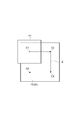
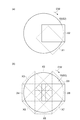
- FIG. 5 is a plan view showing an example of a plurality of irradiated areas.
- each of the three irradiated areas X1, X2, and X3, each of which includes a part of the back surface S2 and is arranged in series along a certain direction, is irradiated with light h ⁇ once.
- one light irradiation may include one pulsed light or two or more pulsed lights.
- a plurality of irradiated regions X1, X2, and X3 are combined so that the adjacent irradiated regions partially overlap each other and the region X including the plurality of irradiated regions X1, X2, and X3 includes the entire back surface S2. Irradiated areas X1, X2, and X3 are arranged.
- the end portion including the end Y1 of the irradiated region X1 and the end portion including the end Y2 of the irradiated region X2 overlap each other.
- the portions located directly above the back surface S2 overlap each other, so that the portion of the back surface S2 located at the end of each irradiated area is overlapped twice or more.
- Light h ⁇ is irradiated.
- the semiconductor member 45 may be difficult to peel off from the support substrate 10. The present inventors presume that this is because the energy of the irradiated light is easily diffused at the end of the irradiated area.
- the width W 1 of the portion where the adjacent irradiated regions overlap may be as long as the semiconductor member 45 can be appropriately peeled off, for example, 0.05 cm or more, 0.1 cm or more, and 1000 cm or less. There may be.
- the ratio of the width W 1 to the width W 0 of the irradiated area may be 0.05 or more, 0.1 or more, or 0.9 or less.
- the widths W 0 and W 1 mean the maximum widths of the irradiated area and the overlapping portion in the direction perpendicular to the outer circumference of the irradiated area, respectively.
- the shape of the irradiated area is not particularly limited, but can be, for example, a rectangle as shown in FIG.
- a light source having a light emitting surface for example, a lamp
- a region in which the light emitting surface is vertically projected onto a plane including the back surface S2 can be regarded as an irradiated region.
- the light source may be a lamp having a light emitting surface that supplies light of substantially uniform intensity (energy amount) over the entire irradiated area. Therefore, for example, the amount of light energy [J / cm 2 ] on the entire light emitting surface of the lamp may be in the range of ⁇ 5.0% of the overall average value.
- the support substrate 10 may be moved with the light source fixed.
- the light source may be moved with the support substrate 10 fixed.
- the light source stops with respect to the support substrate 10 while intermittently moving the position of the light source with respect to the support substrate 10 between the positions corresponding to the irradiated areas X1, X2, and X3, respectively.
- the light h ⁇ is irradiated.
- the order of the irradiated areas to be irradiated with light is arbitrary.
- the form such as the number, size, and position of the plurality of irradiated areas is not limited to the form shown in FIG. 5, and the area in which the plurality of irradiated areas are combined includes the entire back surface S2, and the back surface S2 of each irradiated area is included. It may be set so that the end portion including the above is irradiated with light more than once.
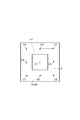
- 6, 7 and 8 are plan views showing other examples of the plurality of irradiated areas, respectively. In FIG. 6, instead of showing the irradiated areas other than the irradiated area X1 to which the first light is irradiated, the centers C1, C2, C3 and C4 of each irradiated area are shown.
- the arrow Z indicates the moving direction of the position (that is, the irradiated area) of the light source with respect to the support substrate 10.
- FIGS. 7 and 8 A similar illustration method is applied in FIGS. 7 and 8.
- the four irradiated areas including the back surface S2 of the support substrate 10 are sequentially irradiated with light four times in a clockwise direction.
- the nine irradiated areas including the back surface S2 of the support substrate 10 are sequentially irradiated with light nine times in a clockwise direction.
- the last irradiated area includes the center of the back surface S2.
- starting from the first irradiated area X1 including the center of the back surface S2 the nine irradiated areas including the back surface S2 of the support substrate 10 are sequentially clockwise 9 times. Light is emitted.
- the plurality of irradiated areas may be sequentially irradiated with light h ⁇ .
- the light h ⁇ is irradiated by the light source fixed to the upper part of the circular back surface S2 of the support substrate 10.
- the support substrate 10 is rotated by 45 ° in the clockwise rotation direction CW, and the irradiated areas X2, X3, X4, X5, X6, X7 and X8.
- the light h ⁇ is irradiated once in the order of.
- Each of the eight irradiated areas X1 to X8 includes a part of the back surface S2.
- the rotation angle of the support substrate 10 at one time is not limited to 45 °, and can be changed to any angle such that the combined region of the plurality of irradiated regions includes the entire back surface S2.
- the direction of rotation may be counterclockwise.
- the method of rotating the support substrate 10 is advantageous in that the moving distance of the support substrate 10 or the light source is small as compared with the method of linearly moving the support substrate 10 or the light source, for example. This method can be particularly easily applied when the back surface S2 of the support substrate 10 is circular.
- the light h ⁇ can be incoherent light or coherent light such as laser light.
- Incoherent light is light that is not coherent, and is an electromagnetic wave having properties such as no interference fringes, low coherence, and low directivity. Incoherent light tends to be attenuated as the optical path length becomes longer.
- Laser light is generally coherent light, whereas light such as sunlight and fluorescent light is incoherent light.
- Incoherent light can also be said to be light excluding laser light.
- the processed semiconductor member can be easily separated from the support substrate even with incoherent light having a relatively small amount of energy.
- incoherent light having a small amount of energy it is possible to suppress damage to a fine structure such as a rewiring layer of a semiconductor member. Since the irradiation area of incoherent light is generally overwhelmingly larger than that of coherent light (that is, laser light), the number of irradiations can be reduced.
- the light h ⁇ may contain infrared rays.
- the light h ⁇ may be pulsed light.
- the light source is not particularly limited, but may be a xenon lamp.
- a xenon lamp is a lamp that utilizes light emission by application / discharge in an arc tube filled with xenon gas. Since the xenon lamp discharges while repeating ionization and excitation, it has a stable continuous wavelength from the ultraviolet light region to the infrared light region. Since the xenon lamp requires a shorter start time than a lamp such as a metal halide lamp, the time required for the process can be significantly shortened. Since it is necessary to apply a high voltage for light emission, high heat is generated instantaneously, but the xenon lamp is also advantageous in that the cooling time is short and continuous work is possible.
- the irradiation conditions of the xenon lamp include the applied voltage, pulse width, irradiation time, irradiation distance (distance between the light source and the temporary fixing material layer), irradiation energy, etc., and these can be arbitrarily set according to the number of irradiations, etc. it can.
- a part of the curable resin layer 31c may adhere as a residue 31c'on the separated semiconductor member 45.
- the attached residue 31c' is removed as shown in FIG. 4 (c).
- the residue 31c' is removed, for example, by washing with a solvent.
- the solvent is not particularly limited, and examples thereof include ethanol, methanol, toluene, xylene, acetone, methyl ethyl ketone, methyl isobutyl ketone, and hexane. These may be used individually by 1 type or in combination of 2 or more type.
- the semiconductor member 45 may be immersed in a solvent or ultrasonically cleaned.
- the semiconductor member 45 may be heated at a low temperature of about 100 ° C. or lower.
- the semiconductor element 60 including the processed semiconductor member 45 can be obtained.
- a semiconductor device can be manufactured by connecting the obtained semiconductor element 60 to another semiconductor element or a substrate for mounting the semiconductor element.
- the obtained resin varnish was applied to the release-treated surface of a polyethylene terephthalate (PET) film (Purex A31, Teijin DuPont Film Co., Ltd., thickness: 38 ⁇ m) using a precision coating machine.
- PET polyethylene terephthalate
- the coating film was dried by heating at 80 ° C. for 10 minutes to form a curable resin layer having a thickness of about 100 ⁇ m.
- a light absorption layer support substrate As a light absorption layer support substrate, a rectangular slide glass having a size of 110 ⁇ 110 mm was prepared. On the prepared slide glass, a titanium layer and a copper layer were formed in this order by sputtering to form a light absorption layer composed of two layers of a titanium layer (thickness: 20 nm) and a copper layer (thickness: 200 nm). In sputtering, after pretreatment by reverse sputtering, a titanium layer and a copper layer were formed by RF sputtering.
- a curable resin layer cut out to a size of 100 ⁇ 100 mm was placed on the light absorption layer formed on the temporary fixing laminate slide glass.
- the curable resin layer was brought into close contact with the light absorption layer by vacuum lamination to obtain a temporary fixing laminate having a laminated structure of a support substrate / light absorption layer / curable resin layer.
- pulsed light was irradiated to each of the three irradiated areas including the back surface of the support substrate with a xenon lamp.
- the ends of the adjacent irradiated regions overlap each other, and the width W 1 of the overlapping portions was 0.75 cm.
- PulseForge (registered trademark) 1300 manufactured by NovaCentrick was used as the xenon lamp.
- the xenon lamp comprises a light emitting surface having a size of 150 mm ⁇ 75 mm and emitting substantially uniform light.
- the wavelength range of the emitted light is 200 nm to 1500 nm.
- One pulsed light having an applied voltage of 800 V and a pulse width of 250 ⁇ s was applied to each irradiated area.
- the amount of energy of each pulsed light irradiated was 3.4 J / cm 2 .
- the semiconductor chip was peeled off without breaking the slide glass.
- Comparative Example From the slide glass side of the temporary fixing laminate similar to the example, the same conditions as in the example were applied to the two irradiated regions in contact with each other at the center of the back surface of the slide glass so that the ends did not overlap. I irradiated the pulsed light with a xenon lamp. After irradiation, it was confirmed that the semiconductor chip was not peeled off at the center of the slide glass.
- Temporary fixing laminate 10 ... Support substrate, 30 ... Temporary fixing material layer, 31, 31A, 31c ... Curable resin layer, 31B, 32 ... Light absorption layer, 40 ... Semiconductor substrate, 41 ... Rewiring layer, 45 ... semiconductor member, 50 ... sealing layer, 60 ... semiconductor element, h ⁇ ... light, S3 ... outermost surface, S1 ... support surface, S2 ... back surface, X ... region including irradiated area, X1, X2, X3 ... Irradiated area.
Landscapes
- Chemical & Material Sciences (AREA)
- Organic Chemistry (AREA)
- Mechanical Treatment Of Semiconductor (AREA)
- Laminated Bodies (AREA)
- Adhesives Or Adhesive Processes (AREA)
- Container, Conveyance, Adherence, Positioning, Of Wafer (AREA)
- Dicing (AREA)
- Adhesive Tapes (AREA)
- Recrystallisation Techniques (AREA)
Priority Applications (8)
| Application Number | Priority Date | Filing Date | Title |
|---|---|---|---|
| CN202080036919.XA CN113840891B (zh) | 2019-05-22 | 2020-05-20 | 半导体装置的制造方法 |
| KR1020217041060A KR102864887B1 (ko) | 2019-05-22 | 2020-05-20 | 반도체 장치를 제조하는 방법 |
| JP2021520818A JP7597025B2 (ja) | 2019-05-22 | 2020-05-20 | 半導体装置を製造する方法 |
| EP20810743.3A EP3974491A4 (en) | 2019-05-22 | 2020-05-20 | SEMICONDUCTOR DEVICE MANUFACTURING PROCESS |
| CN202311062179.9A CN117096040A (zh) | 2019-05-22 | 2020-05-20 | 半导体装置的制造方法 |
| US17/612,224 US12165882B2 (en) | 2019-05-22 | 2020-05-20 | Semiconductor device manufacturing method |
| US18/900,891 US20250046626A1 (en) | 2019-05-22 | 2024-09-30 | Semiconductor device manufacturing method |
| JP2024201669A JP2025032136A (ja) | 2019-05-22 | 2024-11-19 | 半導体装置を製造する方法 |
Applications Claiming Priority (2)
| Application Number | Priority Date | Filing Date | Title |
|---|---|---|---|
| JP2019-096008 | 2019-05-22 | ||
| JP2019096008 | 2019-05-22 |
Related Child Applications (2)
| Application Number | Title | Priority Date | Filing Date |
|---|---|---|---|
| US17/612,224 A-371-Of-International US12165882B2 (en) | 2019-05-22 | 2020-05-20 | Semiconductor device manufacturing method |
| US18/900,891 Continuation US20250046626A1 (en) | 2019-05-22 | 2024-09-30 | Semiconductor device manufacturing method |
Publications (1)
| Publication Number | Publication Date |
|---|---|
| WO2020235597A1 true WO2020235597A1 (ja) | 2020-11-26 |
Family
ID=73458417
Family Applications (1)
| Application Number | Title | Priority Date | Filing Date |
|---|---|---|---|
| PCT/JP2020/019963 Ceased WO2020235597A1 (ja) | 2019-05-22 | 2020-05-20 | 半導体装置を製造する方法 |
Country Status (7)
| Country | Link |
|---|---|
| US (2) | US12165882B2 (https=) |
| EP (1) | EP3974491A4 (https=) |
| JP (2) | JP7597025B2 (https=) |
| KR (1) | KR102864887B1 (https=) |
| CN (2) | CN117096040A (https=) |
| TW (2) | TWI836077B (https=) |
| WO (1) | WO2020235597A1 (https=) |
Families Citing this family (3)
| Publication number | Priority date | Publication date | Assignee | Title |
|---|---|---|---|---|
| WO2019106846A1 (ja) * | 2017-12-01 | 2019-06-06 | 日立化成株式会社 | 半導体装置の製造方法、仮固定材用樹脂組成物、及び仮固定材用積層フィルム |
| US11996384B2 (en) | 2020-12-15 | 2024-05-28 | Pulseforge, Inc. | Method and apparatus for debonding temporarily bonded wafers in wafer-level packaging applications |
| DE102022114911A1 (de) * | 2022-06-14 | 2023-12-14 | Delo Industrie Klebstoffe Gmbh & Co. Kgaa | Verfahren zum Herstellen von elektronischen Baugruppen und elektronische Baugruppe auf Wafer-Ebene |
Citations (5)
| Publication number | Priority date | Publication date | Assignee | Title |
|---|---|---|---|---|
| JP2012126803A (ja) | 2010-12-14 | 2012-07-05 | Sumitomo Bakelite Co Ltd | 仮固定剤および基材の加工方法 |
| JP2013033814A (ja) | 2011-08-01 | 2013-02-14 | Jsr Corp | 基材の処理方法、半導体装置および仮固定用組成物 |
| JP2013534721A (ja) * | 2010-06-16 | 2013-09-05 | スリーエム イノベイティブ プロパティズ カンパニー | ウェーハ支持システム用の変換層を加熱するために光学的調整を施した金属化光 |
| JP2016048729A (ja) * | 2014-08-27 | 2016-04-07 | 株式会社東芝 | 仮接着用支持基板及び半導体デバイスの製造方法 |
| JP2016138182A (ja) | 2015-01-27 | 2016-08-04 | デンカ株式会社 | 仮固定用接着剤組成物、それを用いた部材の仮固定方法及び硬化体残渣の除去方法 |
Family Cites Families (27)
| Publication number | Priority date | Publication date | Assignee | Title |
|---|---|---|---|---|
| US6525493B2 (en) * | 1998-08-26 | 2003-02-25 | Q-Panel Lab Products | Materials test chamber with xenon lamp radiation |
| JP2000260710A (ja) * | 1999-03-11 | 2000-09-22 | Seiko Epson Corp | 半導体装置の製造方法及びアニール装置 |
| US7094451B2 (en) * | 1999-04-07 | 2006-08-22 | Board Of Trustees Of Michigan State University | Chemical functionalization of material surfaces using optical energy and chemicals |
| JP2003224117A (ja) * | 2002-01-31 | 2003-08-08 | Advanced Lcd Technologies Development Center Co Ltd | 絶縁膜の製造装置 |
| DE102004030268B4 (de) * | 2003-06-24 | 2013-02-21 | Fuji Electric Co., Ltd | Verfahren zum Herstellen eines Halbleiterelements |
| US8486742B2 (en) * | 2006-11-21 | 2013-07-16 | Epistar Corporation | Method for manufacturing high efficiency light-emitting diodes |
| JP5257314B2 (ja) * | 2009-09-29 | 2013-08-07 | 大日本印刷株式会社 | 積層体、準備用支持体、積層体の製造方法、及びデバイスの製造方法 |
| US8986497B2 (en) * | 2009-12-07 | 2015-03-24 | Ipg Photonics Corporation | Laser lift off systems and methods |
| JP4948629B2 (ja) | 2010-07-20 | 2012-06-06 | ウシオ電機株式会社 | レーザリフトオフ方法 |
| JP2012069919A (ja) * | 2010-08-25 | 2012-04-05 | Toshiba Corp | 半導体装置の製造方法 |
| JP2012069734A (ja) * | 2010-09-24 | 2012-04-05 | Toshiba Corp | 半導体装置の製造方法 |
| JP2013145808A (ja) * | 2012-01-13 | 2013-07-25 | Sharp Corp | 剥離方法、液晶ディスプレイの製造方法、有機elディスプレイの製造方法、およびタッチパネルの製造方法 |
| JP5977532B2 (ja) | 2012-02-20 | 2016-08-24 | 東京応化工業株式会社 | 支持体分離方法及び支持体分離装置 |
| US20140231012A1 (en) * | 2013-02-15 | 2014-08-21 | Dainippon Screen Mfg, Co., Ltd. | Substrate processing apparatus |
| JP6243616B2 (ja) * | 2013-03-26 | 2017-12-06 | キヤノン株式会社 | 露光装置および物品の製造方法 |
| JP6050170B2 (ja) * | 2013-03-27 | 2016-12-21 | 富士フイルム株式会社 | 半導体装置製造用仮接合用積層体、および、半導体装置の製造方法 |
| CN106463473A (zh) * | 2014-06-26 | 2017-02-22 | 凸版印刷株式会社 | 配线基板、半导体装置以及半导体装置的制造方法 |
| JP6437805B2 (ja) * | 2014-12-03 | 2018-12-12 | 東京応化工業株式会社 | 積層体の製造方法、封止基板積層体の製造方法及び積層体 |
| JP6718736B2 (ja) * | 2015-05-22 | 2020-07-08 | 株式会社Screenホールディングス | 耐熱性有機高分子層の剥離方法およびフレキシブル配線板の製造方法 |
| JP6517643B2 (ja) * | 2015-09-16 | 2019-05-22 | 株式会社ジャパンディスプレイ | 表示装置の製造方法、および、表示装置 |
| JP6524972B2 (ja) * | 2015-09-28 | 2019-06-05 | Jsr株式会社 | 対象物の処理方法、仮固定用組成物、半導体装置及びその製造方法 |
| JP6463664B2 (ja) * | 2015-11-27 | 2019-02-06 | 信越化学工業株式会社 | ウエハ加工体及びウエハ加工方法 |
| JP6649111B2 (ja) * | 2016-02-16 | 2020-02-19 | 東京応化工業株式会社 | 積層体、積層体の製造方法、及び基板の処理方法 |
| EP3469635B1 (de) * | 2017-01-26 | 2020-09-09 | Gross, Leander Kilian | Verfahren und vorrichtung zum trennen verschiedener materialschichten eines verbundbauteils |
| JP6387208B1 (ja) * | 2017-10-26 | 2018-09-05 | 堺ディスプレイプロダクト株式会社 | フレキシブルoledデバイスの製造方法および製造装置 |
| WO2019106846A1 (ja) * | 2017-12-01 | 2019-06-06 | 日立化成株式会社 | 半導体装置の製造方法、仮固定材用樹脂組成物、及び仮固定材用積層フィルム |
| US10505079B2 (en) * | 2018-05-09 | 2019-12-10 | X-Celeprint Limited | Flexible devices and methods using laser lift-off |
-
2020
- 2020-05-20 TW TW109116747A patent/TWI836077B/zh active
- 2020-05-20 US US17/612,224 patent/US12165882B2/en active Active
- 2020-05-20 EP EP20810743.3A patent/EP3974491A4/en active Pending
- 2020-05-20 CN CN202311062179.9A patent/CN117096040A/zh active Pending
- 2020-05-20 TW TW113105693A patent/TWI879437B/zh active
- 2020-05-20 WO PCT/JP2020/019963 patent/WO2020235597A1/ja not_active Ceased
- 2020-05-20 KR KR1020217041060A patent/KR102864887B1/ko active Active
- 2020-05-20 JP JP2021520818A patent/JP7597025B2/ja active Active
- 2020-05-20 CN CN202080036919.XA patent/CN113840891B/zh active Active
-
2024
- 2024-09-30 US US18/900,891 patent/US20250046626A1/en active Pending
- 2024-11-19 JP JP2024201669A patent/JP2025032136A/ja active Pending
Patent Citations (5)
| Publication number | Priority date | Publication date | Assignee | Title |
|---|---|---|---|---|
| JP2013534721A (ja) * | 2010-06-16 | 2013-09-05 | スリーエム イノベイティブ プロパティズ カンパニー | ウェーハ支持システム用の変換層を加熱するために光学的調整を施した金属化光 |
| JP2012126803A (ja) | 2010-12-14 | 2012-07-05 | Sumitomo Bakelite Co Ltd | 仮固定剤および基材の加工方法 |
| JP2013033814A (ja) | 2011-08-01 | 2013-02-14 | Jsr Corp | 基材の処理方法、半導体装置および仮固定用組成物 |
| JP2016048729A (ja) * | 2014-08-27 | 2016-04-07 | 株式会社東芝 | 仮接着用支持基板及び半導体デバイスの製造方法 |
| JP2016138182A (ja) | 2015-01-27 | 2016-08-04 | デンカ株式会社 | 仮固定用接着剤組成物、それを用いた部材の仮固定方法及び硬化体残渣の除去方法 |
Also Published As
| Publication number | Publication date |
|---|---|
| KR102864887B1 (ko) | 2025-09-25 |
| US20220319872A1 (en) | 2022-10-06 |
| EP3974491A1 (en) | 2022-03-30 |
| KR20220012877A (ko) | 2022-02-04 |
| JPWO2020235597A1 (https=) | 2020-11-26 |
| JP2025032136A (ja) | 2025-03-11 |
| TWI836077B (zh) | 2024-03-21 |
| US12165882B2 (en) | 2024-12-10 |
| EP3974491A4 (en) | 2022-07-27 |
| JP7597025B2 (ja) | 2024-12-10 |
| US20250046626A1 (en) | 2025-02-06 |
| TW202422724A (zh) | 2024-06-01 |
| CN117096040A (zh) | 2023-11-21 |
| CN113840891A (zh) | 2021-12-24 |
| CN113840891B (zh) | 2023-08-29 |
| TWI879437B (zh) | 2025-04-01 |
| TW202046421A (zh) | 2020-12-16 |
Similar Documents
| Publication | Publication Date | Title |
|---|---|---|
| US20250046626A1 (en) | Semiconductor device manufacturing method | |
| JP7414005B2 (ja) | 半導体装置の製造方法及び仮固定材用積層フィルム | |
| JP7831522B2 (ja) | 半導体装置を製造する方法、光吸収積層体、及び仮固定用積層体 | |
| CN115668446A (zh) | 临时固定用层叠膜及其制造方法、临时固定用层叠体以及半导体装置的制造方法 | |
| JPWO2020111146A1 (ja) | 半導体装置の製造方法及び仮固定材用積層フィルム | |
| TWI893221B (zh) | 暫時固定用膜、暫時固定用積層體及半導體裝置的製造方法 | |
| JP7388004B2 (ja) | 半導体装置の製造方法 | |
| WO2023032981A1 (ja) | 仮固定用フィルム、仮固定用積層体、及び半導体装置の製造方法 | |
| JP2021111645A (ja) | 仮固定用の樹脂組成物と樹脂フィルム及び半導体装置の製造方法 | |
| WO2022071431A1 (ja) | 半導体装置を製造する方法、仮固定用フィルム材を製造する方法、及び、仮固定用フィルム材 | |
| WO2022181636A1 (ja) | 半導体装置を製造する方法、仮固定用フィルム材を製造する方法、及び、仮固定用フィルム材 |
Legal Events
| Date | Code | Title | Description |
|---|---|---|---|
| 121 | Ep: the epo has been informed by wipo that ep was designated in this application |
Ref document number: 20810743 Country of ref document: EP Kind code of ref document: A1 |
|
| ENP | Entry into the national phase |
Ref document number: 2021520818 Country of ref document: JP Kind code of ref document: A |
|
| NENP | Non-entry into the national phase |
Ref country code: DE |
|
| ENP | Entry into the national phase |
Ref document number: 20217041060 Country of ref document: KR Kind code of ref document: A |
|
| ENP | Entry into the national phase |
Ref document number: 2020810743 Country of ref document: EP Effective date: 20211222 |