WO2020230450A1 - 圧電セラミック電子部品 - Google Patents
圧電セラミック電子部品 Download PDFInfo
- Publication number
- WO2020230450A1 WO2020230450A1 PCT/JP2020/011940 JP2020011940W WO2020230450A1 WO 2020230450 A1 WO2020230450 A1 WO 2020230450A1 JP 2020011940 W JP2020011940 W JP 2020011940W WO 2020230450 A1 WO2020230450 A1 WO 2020230450A1
- Authority
- WO
- WIPO (PCT)
- Prior art keywords
- piezoelectric ceramic
- region
- concentration
- electrodes
- layer
- Prior art date
- Legal status (The legal status is an assumption and is not a legal conclusion. Google has not performed a legal analysis and makes no representation as to the accuracy of the status listed.)
- Ceased
Links
Images





Classifications
-
- H—ELECTRICITY
- H10—SEMICONDUCTOR DEVICES; ELECTRIC SOLID-STATE DEVICES NOT OTHERWISE PROVIDED FOR
- H10N—ELECTRIC SOLID-STATE DEVICES NOT OTHERWISE PROVIDED FOR
- H10N30/00—Piezoelectric or electrostrictive devices
- H10N30/80—Constructional details
- H10N30/85—Piezoelectric or electrostrictive active materials
- H10N30/853—Ceramic compositions
- H10N30/8542—Alkali metal based oxides, e.g. lithium, sodium or potassium niobates
-
- C—CHEMISTRY; METALLURGY
- C04—CEMENTS; CONCRETE; ARTIFICIAL STONE; CERAMICS; REFRACTORIES
- C04B—LIME, MAGNESIA; SLAG; CEMENTS; COMPOSITIONS THEREOF, e.g. MORTARS, CONCRETE OR LIKE BUILDING MATERIALS; ARTIFICIAL STONE; CERAMICS; REFRACTORIES; TREATMENT OF NATURAL STONE
- C04B35/00—Shaped ceramic products characterised by their composition; Ceramics compositions; Processing powders of inorganic compounds preparatory to the manufacturing of ceramic products
- C04B35/01—Shaped ceramic products characterised by their composition; Ceramics compositions; Processing powders of inorganic compounds preparatory to the manufacturing of ceramic products based on oxide ceramics
- C04B35/495—Shaped ceramic products characterised by their composition; Ceramics compositions; Processing powders of inorganic compounds preparatory to the manufacturing of ceramic products based on oxide ceramics based on vanadium, niobium, tantalum, molybdenum or tungsten oxides or solid solutions thereof with other oxides, e.g. vanadates, niobates, tantalates, molybdates or tungstates
-
- H—ELECTRICITY
- H10—SEMICONDUCTOR DEVICES; ELECTRIC SOLID-STATE DEVICES NOT OTHERWISE PROVIDED FOR
- H10N—ELECTRIC SOLID-STATE DEVICES NOT OTHERWISE PROVIDED FOR
- H10N30/00—Piezoelectric or electrostrictive devices
- H10N30/01—Manufacture or treatment
- H10N30/09—Forming piezoelectric or electrostrictive materials
- H10N30/093—Forming inorganic materials
- H10N30/097—Forming inorganic materials by sintering
-
- H—ELECTRICITY
- H10—SEMICONDUCTOR DEVICES; ELECTRIC SOLID-STATE DEVICES NOT OTHERWISE PROVIDED FOR
- H10N—ELECTRIC SOLID-STATE DEVICES NOT OTHERWISE PROVIDED FOR
- H10N30/00—Piezoelectric or electrostrictive devices
- H10N30/50—Piezoelectric or electrostrictive devices having a stacked or multilayer structure
-
- H—ELECTRICITY
- H10—SEMICONDUCTOR DEVICES; ELECTRIC SOLID-STATE DEVICES NOT OTHERWISE PROVIDED FOR
- H10N—ELECTRIC SOLID-STATE DEVICES NOT OTHERWISE PROVIDED FOR
- H10N30/00—Piezoelectric or electrostrictive devices
- H10N30/704—Piezoelectric or electrostrictive devices based on piezoelectric or electrostrictive films or coatings
Definitions
- the present invention relates to piezoelectric ceramic electronic components.
- piezoelectric ceramic electronic components such as ultrasonic sensors, piezoelectric buzzers, and piezoelectric actuators using piezoelectric materials have been widely known. Then, there is an increasing demand for piezoelectric ceramic electronic components that can acquire a large displacement amount even with a small voltage.
- Patent Document 1 includes a piezoelectric ceramic element body in which internal electrodes and piezoelectric ceramic layers are alternately laminated and sintered, and a piezoelectric ceramic electronic component in which an external electrode is formed on the surface of the piezoelectric ceramic element body. It is disclosed.
- the internal electrode contains Ni as a main component, and the piezoelectric ceramic layer has a general formula [100 ⁇ (1-x) (K1 -ab Na).
- x, a, b, c, ⁇ , and ⁇ are 0.005 ⁇ x ⁇ 0.1 and 0 ⁇ , respectively.
- Patent Document 2 discloses a piezoelectric ceramic electronic component in which an external electrode is formed on the surface of a piezoelectric ceramic element.
- the piezoelectric ceramic element is formed of an alkali niobate compound having a perovskite-type structure as a main component, contains Ga as a sub component, and contains Nd and Dy. At least one of these elements is contained, and the piezoelectric ceramic element is divided into a surface layer region and a surface layer outer region excluding the surface layer region, and the surface layer region is Ga with respect to Nb.
- Patent Document 2 describes that the ceramic element preferably contains Mn as a sub-component.
- Patent Document 3 describes the first electrode layer, the first oxide layer laminated on the first electrode layer, the second oxide layer laminated on the first oxide layer, and the second oxide layer.
- a piezoelectric thin film laminate comprising a laminated piezoelectric thin film is disclosed.
- the electrical resistivity of the first oxide layer is higher than the electrical resistivity of the second oxide layer, and the first oxide layer contains K, Na and
- the piezoelectric thin film contains Nb and is characterized by containing (K, Na) NbO 3 .
- a piezoelectric ceramic layer or a piezoelectric ceramic element body is formed by firing.
- the piezoelectric thin film laminate described in Patent Document 3 the piezoelectric thin film is formed by a thin film forming method such as a sputtering method or a chemical vapor deposition method.
- Patent Document 1 when a potassium niobate sodium compound, which is a piezoelectric material, is fired in a reducing atmosphere, oxygen vacancies (hereinafter referred to as oxygen defects) are likely to be formed inside, causing sintering defects. ..
- oxygen defects oxygen vacancies
- Patent Documents 1 and 2 describe that Mn is added to a potassium niobate sodium compound and Mn is dissolved in the potassium niobate sodium compound to obtain sinterability in a reducing atmosphere. It is stated to improve.
- Mn added to the potassium niobate sodium compound plays an important role in piezoelectric ceramic electronic components.
- the piezoelectric thin film is formed by the thin film forming method as in Patent Document 3, the concentration of the element contained in each layer can be adjusted.
- the piezoelectric ceramic layer is formed by firing as in Patent Documents 1 and 2, elements such as Mn are diffused during firing, and alkali metal elements such as K and Na are volatilized. Therefore, it is difficult to control the concentration of the elements contained in the piezoelectric ceramic layer. Therefore, it can be said that there is room for improvement in suppressing the decrease in insulation resistance in the piezoelectric ceramic electronic component provided with the ceramic sintered body.
- the present invention has been made to solve the above problems, and is a piezoelectric ceramic provided with a piezoelectric ceramic layer composed of a ceramic sintered body and capable of suppressing a decrease in insulation resistance even when driven for a long time.
- the purpose is to provide electronic components.
- the piezoelectric ceramic electronic component of the present invention includes a piezoelectric ceramic element including one layer or a plurality of piezoelectric ceramic layers, and a plurality of electrodes provided on the surface or inside of the piezoelectric ceramic element.
- the piezoelectric ceramic layer is composed of a ceramic sintered body containing a potassium niobate sodium compound and Mn.
- the piezoelectric ceramic layer sandwiched between adjacent electrodes is divided into three equal parts in the thickness direction to form a first region, a second region, and a third region in this order from one electrode side to the other electrode side, the first region is described above.
- the Mn concentration contained in the second region is higher than the Mn concentration contained in the third region.
- a piezoelectric ceramic electronic component provided with a piezoelectric ceramic layer composed of a ceramic sintered body and capable of suppressing a decrease in insulation resistance even when driven for a long time.
- FIG. 1 is a cross-sectional view schematically showing an example of a laminated piezoelectric actuator according to an embodiment of the piezoelectric ceramic electronic component of the present invention.
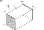
- FIG. 2 is a perspective view of a laminated piezoelectric actuator according to an embodiment of the piezoelectric ceramic electronic component of the present invention.
- FIG. 3 is a first schematic view for explaining a position for evaluating the Mn concentration contained in the piezoelectric ceramic layer.
- FIG. 4 is a second schematic view for explaining a position for evaluating the Mn concentration contained in the piezoelectric ceramic layer.
- FIG. 5 (a) is an example of a mapping image of Ni element
- FIG. 5 (b) is an example of a mapping image of Mn element.
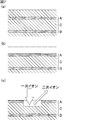
- FIG. 6 (a), 6 (b), 6 (c) and 6 (d) are schematics for explaining the procedure for dividing the piezoelectric ceramic layer into a first region, a second region and a third region. It is a figure. 7 (a), 7 (b) and 7 (c) are schematic views for explaining the procedure of D-SIMS analysis.
- FIG. 8 is a perspective view schematically showing a ceramic green sheet obtained in the manufacturing process of the laminated piezoelectric actuator.
- 9 (a) is a Ni mapping image
- FIG. 9 (b) is an Mn mapping image
- FIG. 9 (c) is a Li mapping image
- FIG. 9 (d) is a graph showing the distribution of Mn concentration
- FIG. 9 (e) is a graph.
- FIG. 10 (a) is a Ni mapping image
- FIG. 10 (b) is an Mn mapping image
- FIG. 10 (c) is a Li mapping image
- FIG. 10 (d) is a graph showing the distribution of Mn concentration
- FIG. 10 (e) is a graph. It is a graph which shows the distribution of Li concentration.
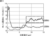
- FIG. 11 is a graph showing the distribution of the Mn / Li concentration ratio in Sample 3 and Sample 6.
- the piezoelectric ceramic electronic component of the present invention will be described.
- the present invention is not limited to the following configurations, and can be appropriately modified and applied without changing the gist of the present invention. It should be noted that a combination of two or more of the individual desirable configurations described below is also the present invention.
- the piezoelectric ceramic electronic component of the present invention includes a piezoelectric ceramic element including one layer or a plurality of piezoelectric ceramic layers, and a plurality of electrodes provided on the surface or inside of the piezoelectric ceramic element.
- the electrode provided on the surface of the piezoelectric ceramic body is referred to as an external electrode
- the electrode provided inside the piezoelectric ceramic body is referred to as an internal electrode.
- the piezoelectric ceramic electronic component includes a plurality of external electrodes and a plurality of internal electrodes as electrodes.
- the piezoelectric ceramic electronic component of the present invention may include a plurality of internal electrodes or a single layer of internal electrodes. Further, the piezoelectric ceramic electronic component of the present invention may not include an internal electrode but may include only a plurality of external electrodes.
- the piezoelectric ceramic body includes one piezoelectric ceramic layer.
- FIG. 1 is a cross-sectional view schematically showing an example of a laminated piezoelectric actuator according to an embodiment of the piezoelectric ceramic electronic component of the present invention.
- FIG. 2 is a perspective view of a laminated piezoelectric actuator according to an embodiment of the piezoelectric ceramic electronic component of the present invention.
- FIG. 1 corresponds to a sectional view taken along line II of the laminated piezoelectric actuator shown in FIG.
- the laminated piezoelectric actuator 10 shown in FIGS. 1 and 2 is provided on the surface of the piezoelectric ceramic element 1 including the piezoelectric ceramic layers 3a, 3b, 3c, 3d, 3e, 3f, 3g and 3h, and the surface of the piezoelectric ceramic element 1.
- the external electrodes 2a and 2b and the internal electrodes 4a, 4b, 4c, 4d, 4e, 4f and 4g provided inside the piezoelectric ceramic element 1 are provided.
- the external electrodes 2a and 2b are provided at both ends of the piezoelectric ceramic element 1.
- the external electrodes 2a and 2b are made of a conductive material such as Ag.
- the piezoelectric ceramic layers 3a, 3b, 3c, 3d, 3e, 3f, 3g and 3h and the internal electrodes 4a, 4b, 4c, 4d, 4e, 4f and 4g are formed. They are stacked alternately.
- the piezoelectric ceramic layers 3a, 3b, 3c, 3d, 3e, 3f, 3g and 3h are composed of a ceramic sintered body described later.
- the internal electrodes 4a, 4b, 4c, 4d, 4e, 4f and 4g are made of, for example, a conductive material containing Ni as a main component.
- one ends of the internal electrodes 4a, 4c, 4e and 4g are electrically connected to one external electrode 2a, and one ends of the internal electrodes 4b, 4d and 4f are electrically connected to the other external electrode 2b. It is connected.
- a voltage is applied between the external electrode 2a and the external electrode 2b, the voltage is displaced in the stacking direction indicated by the arrow Z due to the piezoelectric longitudinal effect.
- the piezoelectric ceramic layer is composed of a ceramic sintered body containing a sodium niobate (KNN) -based compound and Mn.
- KNN sodium niobate
- the KNN compound is the main component of the ceramic sintered body.
- the "main component” means a component having the largest abundance ratio (mol%) in the ceramic sintered body, and preferably means a component having an abundance ratio of more than 50 mol%.
- the KNN-based compound has a perovskite-type structure and is represented by the general formula (K, Na) NbO 3 .
- the composition of the KNN-based compound is not particularly limited.
- the KNN-based compound preferably contains K as an alkali metal element, and more preferably contains at least one of Na and Li in addition to K. Further, the KNN-based compound may contain other elements in addition to the above-mentioned alkali metal element, and may contain, for example, Ta.
- the ceramic sintered body preferably contains a KNN-based compound in an amount of more than 50 mol%, more preferably 90 mol% or more.
- the ceramic sintered body preferably contains 99 mol% or less of the KNN compound, and may contain 85 mol% or less.
- Mn is a sub-component of the ceramic sintered body. As described above, Mn forms an electrical pair with the oxygen defect, hinders the movement of the oxygen defect, and plays a role of suppressing a decrease in insulation resistance.
- the ceramic sintered body preferably contains Mn of 2 mol% or more.
- Mn hinders the movement of oxygen defects and suppresses the decrease in insulation resistance, but when the amount of Mn added is large, a heterogeneous phase containing Mn is formed in the ceramic sintered body. Since this heterogeneous phase does not exhibit piezoelectricity, if there are many different phases, the piezoelectricity of the entire ceramic sintered body decreases. Therefore, the ceramic sintered body preferably contains Mn in an amount of 15 mol% or less, and more preferably 5 mol% or less.
- the ceramic sintered body may contain other components for the purpose of improving the piezoelectric characteristics and the like.
- M2 represents at least one divalent element selected from the group consisting of the general formula M2M4O 3 (M2 is Ba, Ca and Sr, and M4 is Zr, Sn and It may contain an appropriate amount of a compound represented by at least one tetravalent element selected from the group consisting of Hf). This makes it possible to further improve the piezoelectric characteristics.
- the ceramic sintered body may contain an element other than Mn as a sub-component.
- the ceramic sintered body is composed of a plurality of crystallites.
- the particle size of the crystallite is preferably 10 ⁇ m or less.
- the particle size of the crystallite is, for example, 0.1 ⁇ m or more.
- the ceramic sintered body contains, for example, 90 mol% or more of (K 1-ab Na a Li b ) NbO 3 (0 ⁇ a ⁇ 0.9, 0 ⁇ b ⁇ 0.1), and 2 mol% or more of Mn. It is composed of crystallites containing 15 mol% or less and having a particle size of 10 ⁇ m or less.
- the piezoelectric ceramic layer sandwiched between adjacent electrodes is divided into three equal parts in the thickness direction, and the first region, the second region, and the second region are sequentially divided from one electrode side to the other electrode side.
- the Mn concentration contained in the second region is higher than the Mn concentration contained in the first region and the third region.
- the piezoelectric ceramic electronic component of the present invention since a region having a high Mn concentration exists in the piezoelectric ceramic layer sandwiched between adjacent electrodes, oxygen defects contained in the piezoelectric ceramic layer are maintained while maintaining high piezoelectric characteristics. Movement can be prevented.
- the piezoelectric ceramic layer sandwiched between adjacent electrodes is, for example, a piezoelectric ceramic layer sandwiched between a set of internal electrodes adjacent in the thickness direction.
- the piezoelectric ceramic layer sandwiched between adjacent electrodes may be a piezoelectric ceramic layer sandwiched between a set of internal electrodes and external electrodes adjacent in the thickness direction.
- the piezoelectric ceramic layer sandwiched between adjacent electrodes may be a piezoelectric ceramic layer sandwiched between a set of external electrodes adjacent in the thickness direction.
- a piezoelectric ceramic layer sandwiched between a set of internal electrodes adjacent to each other in the thickness direction means that, in a piezoelectric ceramic element, among a pair of internal electrodes connected to different external electrodes, the electrode spacing is It means a piezoelectric ceramic layer sandwiched between the smallest pair of internal electrodes (hereinafter referred to as counter electrodes).
- FIG. 3 is a first schematic view for explaining a position for evaluating the Mn concentration contained in the piezoelectric ceramic layer.
- the external electrodes 2a and 2b are provided at both ends of the piezoelectric ceramic element, among the pair of the internal electrode connected to the external electrode 2a and the internal electrode connected to the external electrode 2b.
- to evaluate the Mn concentration electrode spacing is contained in the piezoelectric ceramic layer sandwiched between the pair P 1 of the smallest internal electrodes.
- both Mn concentration contained in the piezoelectric ceramic layer sandwiched between the pair P 2 of the internal electrodes connected to the same external electrode 2a or 2b is not subject to evaluation.
- FIG. 4 is a second schematic view for explaining a position for evaluating the Mn concentration contained in the piezoelectric ceramic layer.
- external electrodes 2a and 2b are provided at both ends of the piezoelectric ceramic body, and external electrodes 2c are provided on both sides of the piezoelectric ceramic body.
- Fig In 4 among pairs of internal electrodes connected to the internal electrodes and the external electrodes 2c connected to the external electrodes 2a and 2b, piezoelectric ceramic layer electrode spacing is sandwiched pair P 3 of the smallest internal electrodes The Mn concentration contained is evaluated. As shown in FIG.
- the Mn concentration may be evaluated by selecting the position where the distance between the internal electrodes is the smallest in the region where the internal electrodes face each other. Similar to FIG. 3, both Mn concentration also contained in the piezoelectric ceramic layer sandwiched between a pair P 4 of the internal electrodes are connected to the same external electrode 2a, 2b or 2c is outside the scope of evaluation.
- the distribution of Mn concentration contained in each region of the piezoelectric ceramic layer is obtained by WDX (wavelength dispersive fluorescent X-ray) as follows. Further, the distribution of the Mn concentration contained in each region of the piezoelectric ceramic layer can also be obtained by Dynamic SIMS (D-SIMS) described later.
- D-SIMS Dynamic SIMS
- the piezoelectric ceramic electronic component is embedded in a resin such as urethane resin and polished from the side surface in the stacking direction to expose the cross section.
- the visual field is adjusted so that the counter electrode described above fits in one visual field and the counter electrode is substantially parallel to the vertical axis of the visual field, and the main component of the internal electrode is used.
- Element mapping analysis is performed with the metal element, for example, Ni, as the target element.
- element mapping analysis with Mn as the target element is performed.
- the width of the field of view it is desirable that the length of one side of the field of view is 10 times or more the average particle size of the ceramic sintered body, and more preferably 20 times or more. This is because heterogeneous phases are likely to occur in KNN compounds, and when the number of particles contained in one field of view is small, the distribution state of elements cannot be correctly grasped.
- FIG. 5 (a) is an example of a mapping image of Ni element
- FIG. 5 (b) is an example of a mapping image of Mn element.
- the region where Ni exists is the internal electrode A and the internal electrode B
- the region sandwiched between the internal electrode A and the internal electrode B is the piezoelectric ceramic layer C.
- the mapping image of the Mn element shown in FIG. 5B it can be confirmed that a region having a high Mn concentration exists near the center of the piezoelectric ceramic layer C, and Mn is also contained in the internal electrode A and the internal electrode B. It can be confirmed that it exists.
- 6 (a), 6 (b), 6 (c) and 6 (d) are schematics for explaining the procedure for dividing the piezoelectric ceramic layer into a first region, a second region and a third region. It is a figure.
- the peak value of the detected amount of the metal element in the visual field is read. A portion where a detected amount of 1/2 or more of the peak value of the detected amount is obtained is identified as an electrode portion, and a portion where a detected amount of less than 1/2 is obtained is identified as a ceramic portion.
- Boundaries are defined as follows for the interface between the internal electrode A and the piezoelectric ceramic layer C and the interface between the internal electrode B and the piezoelectric ceramic layer C shown in FIG. 6 (a).
- Lc a curve that is a set of Lc is obtained in the range from the left end of the field of view to the right end of the field of view (from the upper end to the lower end in FIG. 6B). If the interface between the internal electrode A and the piezoelectric ceramic layer C does not exist on the straight line L some distance from the left end of the field of view, Lc may be interrupted.
- the Mn concentration is calculated by quantifying the amount of fluorescent X-rays detected in each pixel of the mapping analysis result and calculating the average value for each region.
- the values of c m3 may be the same or different.
- the value of c m2 / c m1 and the value of c m2 / c m3 are preferably larger than 1.0, and more preferably 1.2 or more, respectively.
- the value of c m @ 2 / c m1, and the value of c m @ 2 / c m3, respectively, is preferably 2.0 or less, more preferably 1.7 or less.
- the piezoelectric ceramic layers sandwiched between the adjacent electrodes are the first Mn low-concentration layer and the Mn in order from one electrode side to the other electrode side. It is composed of a high-concentration layer and a second Mn low-concentration layer, and has a Mn concentration contained in the Mn high-concentration layer as compared with the Mn concentration contained in the first Mn low-concentration layer and the second Mn low-concentration layer. Is preferably high. That is, in the piezoelectric ceramic layer sandwiched between the adjacent electrodes, it is preferable that the layer having a high Mn concentration is sandwiched between the layers having a low Mn concentration in the thickness direction thereof. This ensures that the movement of oxygen defects is prevented.
- the Mn high concentration layer is preferably thicker than the first Mn low concentration layer and the second Mn low concentration layer.
- the thickness of the first Mn low-concentration layer may be the same as or different from the thickness of the second Mn low-concentration layer.
- the piezoelectric ceramic layer sandwiched between adjacent electrodes contains Li.
- Li When Li is contained in the piezoelectric ceramic layer, the sinterability in a reducing atmosphere is improved, and the Mn concentration is easily distributed in layers in the piezoelectric ceramic layer. As a result, the insulation resistance life during DC drive can be further extended.
- the Li concentration contained in the piezoelectric ceramic layer sandwiched between the adjacent electrodes is preferably 0.03% by weight or more.
- the Li concentration contained in the piezoelectric ceramic layer sandwiched between the adjacent electrodes is preferably 0.06% by weight or less.
- the piezoelectric ceramic layer sandwiched between the adjacent electrodes has an segregation region having a Mn / Li concentration ratio of 4 or more in terms of molar ratio.
- the Li concentration is lower than the Mn concentration, it is considered that the above-mentioned lithium manganate is less likely to be formed, and the effect of preventing the movement of oxygen defects by Mn can be sufficiently obtained.
- the upper limit of the Mn / Li concentration ratio is not particularly limited, but for example, the Mn / Li concentration ratio is 15.0 or less in terms of molar ratio.
- the thickness of the segregation region where the Mn / Li concentration ratio is 4 or more in terms of molar ratio is preferably 0.50 times or more, preferably 0.55 times or more, with respect to the thickness of the piezoelectric ceramic layer in which the segregation region exists. More preferably.
- the thickness of the segregation region where the Mn / Li concentration ratio is 4 or more in terms of molar ratio is 1 time or less and 0.90 times or less the thickness of the piezoelectric ceramic layer in which the segregation region exists. It is more preferably 0.80 times or less, and even more preferably 0.70 times or less.
- the existence of the segregation region here is defined as follows.
- the piezoelectric ceramic element is cut and polished into a cross section parallel to the thickness direction and the long side direction, and on this surface, the piezoelectric ceramic layer and a plurality of internal electrodes or external electrodes are inserted, and the internal electrodes are vertical or horizontal in the field of view. Observe using a scanning electron microscope (SEM) or the like in a field that is substantially parallel to the axis. In this field of view, the average thickness of the piezoelectric ceramic layer sandwiched between one set of internal electrodes or one set of external electrodes or one set of internal electrodes and external electrodes and does not contain an electrode inside is t ⁇ m.
- the element distribution is set for Mn and Li, and elements that are abundantly contained in the electrodes and hardly contained in the ceramic portion, for example, Ni.
- the element distribution data first, for the elements that are contained in a large amount in the electrode and hardly contained in the ceramic part, the average value of the detected values in each pixel in the field of view is used as a threshold value, and the region lower than this value is determined as the ceramic part. To do.
- this rectangular area is about a rectangular area in which the direction substantially parallel to the electrode portion is from one end to the other end of the visual field and the direction substantially perpendicular to the electrode portion is 1 ⁇ m.
- the average amount of Mn and Li in the above is measured as a molar amount, and a region in which the concentration ratio of Mn / Li is 4 or more in terms of molar ratio is defined as a segregation region.
- the distribution of Li concentration and Mn concentration contained in the piezoelectric ceramic layer can be obtained by D-SIMS as follows, for example.
- 7 (a), 7 (b) and 7 (c) are schematic views for explaining the procedure of D-SIMS analysis.
- 7 (a), 7 (b) and 7 (c) show schematic views, which are different from the actual size of the sputtered region.
- the sample shown in FIG. 7A is polished to the position of the internal electrode A in front of the piezoelectric ceramic layer C to be measured.
- FIG. 7 (c) while excavating the sample by ion sputtering using primary ions (O 2 + ions, etc.) in D-SIMS, secondary ions (Li + ions, Mn) ejected from the element at that time are excavated. 2+ ions, etc.) are detected by a mass spectrometer. In this way, the amount of contained elements with respect to the processing depth of ion sputtering is analyzed.
- the size of the sputtering region is 60 ⁇ m square, and the secondary ion detection target range is 12 ⁇ m square. If the distance between the internal electrodes is long (for example, 15 ⁇ m or more) and it is difficult to excavate only by ion sputtering, the element is divided into a plurality of pieces, polished in parallel with the internal electrodes, and D- SIMS analysis may be performed, and the analysis results may be combined after considering the amount of polishing.
- the portion up to 1/2 of the peak value of the detected amount is identified as the electrode portion, and the portion less than 1/2 is identified as the ceramic portion.
- a comparative ceramic sample having a known Mn amount and Li amount is analyzed at the same time, a calibration curve is prepared from the detected amount by D-SIMS, and the detected amount is calibrated from the measured value.
- the ceramic sample for comparison is a sintered body containing KNN as a main component and containing Mn and Li, and it is desirable that the composition distribution is uniform.
- As ceramic sample for comparison for example a (K 0.45 Na 0.50 Li 0.05) (Nb 0.95 Mn 0.05) O 3, to produce a sintered body containing no internal electrodes, previously ICP The absolute value of the composition is evaluated by such means. Further, it is desirable to confirm that the composition distribution inside the comparative ceramic sample is sufficiently small by dividing it into D-SIMS or small pieces and analyzing the composition distribution by ICP or the like.
- the ceramic sample for comparison measure the Mn concentration and Li concentration using D-SIMS with the size of the sputtering region set to 60 ⁇ m square and the secondary ion detection target range set to 12 ⁇ m square, and let the values be a.
- a comparative ceramic sample prepared under the same conditions is sufficiently dissolved in nitric acid having a concentration of 1 N or more heated to 40 ° C. or higher, analyzed by ICP or the like, and the value is defined as b.
- the absolute amount of composition is calculated from the detected value of D-SIMS by multiplying the detected value x of D-SIMS by b / a.
- the respective molar amounts are calculated from the Mn amount and Li amount obtained by the above method, and the molar ratio of Mn and Li is calculated from the obtained molar amount.
- the region where the molar ratio is 4 or more is defined as the segregation region, and the ratio of the thickness of the segregation region to the thickness of the piezoelectric ceramic layer in which the segregation region exists is calculated.
- a K compound containing K, an Nb compound containing Nb, and an Mn compound containing divalent Mn are prepared.
- a Na compound containing Na, a Li compound containing Li, and the like are prepared.
- the form of the compound may be an oxide, a carbonate, or a hydroxide.
- these weighed materials are put into a ball mill containing a pulverizing medium such as PSZ balls, and sufficiently wet-pulverized under a solvent such as ethanol to obtain a mixture.
- a pulverizing medium such as PSZ balls
- the obtained mixture is dried, it is calcined and synthesized at a predetermined temperature (for example, 800 ° C. or higher and 1000 ° C. or lower) to obtain a calcined product.
- a predetermined temperature for example, 800 ° C. or higher and 1000 ° C. or lower
- a ceramic green sheet is produced by molding using a doctor blade method or the like.
- a conductive paste for an internal electrode containing a conductive material such as Ni as a main component is used, and a conductive layer having a predetermined shape is formed on the ceramic green sheet by screen printing.
- FIG. 8 is a perspective view schematically showing a ceramic green sheet obtained in the manufacturing process of the laminated piezoelectric actuator.
- a ceramic laminate in which ceramic green sheets 6a, 6b, 6c, 6d, 6e, 6f and 6g and conductive layers 5a, 5b, 5c, 5d, 5e, 5f and 5g are alternately laminated is produced.
- the obtained ceramic laminate is cut to a predetermined size, placed on an alumina firing jig, debindered at a predetermined temperature (for example, 250 ° C. or higher and 500 ° C. or lower), and then debindered at a predetermined temperature in a reducing atmosphere. (For example, 1000 ° C. or higher and 1160 ° C. or lower) is fired to form a piezoelectric ceramic element 1 in which internal electrodes 4a, 4b, 4c, 4d, 4e, 4f and 4g are embedded.
- the conductive layer containing Ni as the main component and the ceramic green sheet containing the KNN compound as the main component it is necessary to fire in a reducing atmosphere.
- the Mn concentration In order for the Mn concentration to have a layered distribution in the piezoelectric ceramic layer, it is important that a sufficient reducing atmospheric gas flows in with respect to the internal volume of the firing furnace and that the object to be fired sufficiently comes into contact with the atmospheric gas. .. Therefore, it is preferable to put a spacer under the object to be fired to perform firing. Further, it is preferable to introduce a gas of 0.1 a (L / min) or more with respect to the internal volume a (L) of the firing furnace.
- the oxygen partial pressure of the gas is preferably maintained at the equilibrium oxygen partial pressure of Ni and NiO or a value lower than that so that Ni is not oxidized.
- Li is preferably added in order to improve the sinterability, but on the other hand, it is necessary to reduce the Li concentration in the piezoelectric ceramic layer in order to form the segregation region described above.
- the method for adjusting the Li concentration include a method for adjusting the amount charged when preparing the ceramic raw material, a method for adjusting the remaining Li amount by adjusting the flow conditions of the reducing atmosphere gas, and the like. ..
- a conductive paste for an external electrode made of a conductive material such as Ag is applied to both ends of the piezoelectric ceramic element 1, and the external electrode is baked at a predetermined temperature (for example, 750 ° C. or higher and 850 ° C. or lower).
- a predetermined temperature for example, 750 ° C. or higher and 850 ° C. or lower.
- the laminated piezoelectric actuator 10 is manufactured by performing a predetermined polarization process.
- the external electrodes 2a and 2b may be formed by a thin film forming method such as a sputtering method or a vacuum vapor deposition method, as long as they have good adhesion to the piezoelectric ceramic element 1.
- the calcined powder was dispersed with a binder, a dispersant, a surfactant, and an organic solvent containing ethanol as a main component to obtain a slurry containing a calcined raw material.
- the obtained slurry containing the calcined raw material was applied onto a carrier film and dried to prepare a ceramic green sheet containing the calcined raw material.
- a ceramic green sheet was cut, a conductive layer was printed using a conductive paste for internal electrodes containing Ni as a main component, and then laminated and crimped to prepare a laminated crimped body.
- the laminated pressure-bonded body After cutting the laminated pressure-bonded body, it was placed on an alumina firing jig and degreased. Then, by firing while controlling the oxygen partial pressure, a laminated sintered body containing an internal electrode containing Ni as a main component was produced. The oxygen partial pressure was controlled so as to be lower than the equilibrium oxygen partial pressure of Ni and NiO at each temperature during firing.
- the firing temperature was 1100 ° C.
- firing was carried out by introducing a reducing mixed gas of 0.1 a (L / min) or more into the internal volume a (L) of the firing furnace. Firing was carried out by inserting a spacer under the calcined body so that a sufficient reducing atmospheric gas was allowed to flow into the internal volume of the calcining furnace and the calcined body was sufficiently in contact with the atmospheric gas.
- Samples 2-4 A laminated pressure-bonded body was produced by the same method as in Sample 1.
- the amount of Li charged was changed to 0.25 times that of Sample 1, and a laminated sintered body was prepared under the same conditions as in Sample 1 except that.
- sample 3 the flow rate of the atmospheric gas of sample 2 was changed to 1.2 times, and in sample 4, the flow rate of the atmospheric gas of sample 2 was changed to 1.4 times.
- laminated sintering was performed under the same conditions as sample 2. The body was made.
- Example 5 A laminated sintered body was prepared by the same method as in Sample 1 except that Li was removed from the charged composition of the ceramic raw material.
- Example 6 A laminated pressure-bonded body was produced by the same method as in Sample 1. After degreasing the laminated pressure-bonded body, the gas flow rate was changed so that it was less than 0.1 a (L / min) with respect to the internal volume a (L) of the firing furnace, and other than that, the laminated firing was performed under the same conditions as sample 1. A knot was made. The oxygen partial pressure was controlled so as to be lower than the equilibrium oxygen partial pressure of Ni and NiO.
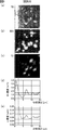
- 9 (a), 9 (b), 9 (c), 9 (d) and 9 (e) show the analysis results of the Mn concentration and the Li concentration of the sample 6.
- 9 (a) is a Ni mapping image
- FIG. 9 (b) is an Mn mapping image
- FIG. 9 (c) is a Li mapping image
- FIG. 9 (d) is a graph showing the distribution of Mn concentration
- FIG. 9 (e) is a graph. It is a graph which shows the distribution of Li concentration.
- 10 (a), 10 (b), 10 (c), 10 (d) and 10 (e) show the analysis results of the Mn concentration and the Li concentration of the sample 3.
- 10 (a) is a Ni mapping image
- FIG. 10 (b) is an Mn mapping image
- FIG. 10 (c) is a Li mapping image
- FIG. 10 (d) is a graph showing the distribution of Mn concentration
- FIG. 10 (e) is a graph. It is a graph which shows the distribution of Li concentration.
- FIG. 11 is a graph showing the distribution of the Mn / Li concentration ratio in Sample 3 and Sample 6. From FIG. 11, it can be confirmed that in the sample 3, there is an segregation region in which the Mn / Li concentration ratio is 4 or more in terms of molar ratio.
- Table 3 further shows the thickness of the piezoelectric ceramic layer when the Li concentration contained in the piezoelectric ceramic layer and the region where the Mn / Li concentration ratio in the piezoelectric ceramic layer is 4 or more in terms of molar ratio are defined as segregation regions. The ratio of the thickness of the segregated region is shown.
- sample 6 has a short life when driven by DC. It is considered that this is because the Mn concentration does not form a layered structure in the piezoelectric ceramic layer, and the movement of oxygen defects cannot be sufficiently prevented.
Landscapes
- Chemical & Material Sciences (AREA)
- Engineering & Computer Science (AREA)
- Ceramic Engineering (AREA)
- Materials Engineering (AREA)
- Manufacturing & Machinery (AREA)
- Inorganic Chemistry (AREA)
- Structural Engineering (AREA)
- Organic Chemistry (AREA)
- Compositions Of Oxide Ceramics (AREA)
Priority Applications (4)
| Application Number | Priority Date | Filing Date | Title |
|---|---|---|---|
| DE112020001337.5T DE112020001337B4 (de) | 2019-05-14 | 2020-03-18 | Piezoelektrisches keramisches elektronisches Bauteil |
| CN202080035593.9A CN113853692B (zh) | 2019-05-14 | 2020-03-18 | 压电陶瓷电子部件 |
| JP2021519288A JP7151884B2 (ja) | 2019-05-14 | 2020-03-18 | 圧電セラミック電子部品 |
| US17/508,567 US12245511B2 (en) | 2019-05-14 | 2021-10-22 | Piezoelectric ceramic electronic component |
Applications Claiming Priority (2)
| Application Number | Priority Date | Filing Date | Title |
|---|---|---|---|
| JP2019091326 | 2019-05-14 | ||
| JP2019-091326 | 2019-05-14 |
Related Child Applications (1)
| Application Number | Title | Priority Date | Filing Date |
|---|---|---|---|
| US17/508,567 Continuation US12245511B2 (en) | 2019-05-14 | 2021-10-22 | Piezoelectric ceramic electronic component |
Publications (1)
| Publication Number | Publication Date |
|---|---|
| WO2020230450A1 true WO2020230450A1 (ja) | 2020-11-19 |
Family
ID=73290188
Family Applications (1)
| Application Number | Title | Priority Date | Filing Date |
|---|---|---|---|
| PCT/JP2020/011940 Ceased WO2020230450A1 (ja) | 2019-05-14 | 2020-03-18 | 圧電セラミック電子部品 |
Country Status (5)
| Country | Link |
|---|---|
| US (1) | US12245511B2 (https=) |
| JP (1) | JP7151884B2 (https=) |
| CN (1) | CN113853692B (https=) |
| DE (1) | DE112020001337B4 (https=) |
| WO (1) | WO2020230450A1 (https=) |
Citations (3)
| Publication number | Priority date | Publication date | Assignee | Title |
|---|---|---|---|---|
| JP2009242167A (ja) * | 2008-03-31 | 2009-10-22 | Tdk Corp | 圧電磁器及びそれを用いた圧電素子 |
| JP2011091234A (ja) * | 2009-10-23 | 2011-05-06 | Seiko Epson Corp | 液体噴射ヘッド、液体噴射装置及びアクチュエーター装置 |
| JP2014107563A (ja) * | 2012-11-28 | 2014-06-09 | Tdk Corp | 圧電素子、圧電アクチュエータ、及び圧電センサ、並びにハードディスクドライブ、及びインクジェットプリンタ装置 |
Family Cites Families (12)
| Publication number | Priority date | Publication date | Assignee | Title |
|---|---|---|---|---|
| JPS6439132A (en) | 1987-08-04 | 1989-02-09 | Matsushita Electric Industrial Co Ltd | Private radio paging receiver |
| JPH0786613B2 (ja) | 1987-10-06 | 1995-09-20 | 凸版印刷株式会社 | 液晶表示素子の配向装置及びその配向方法 |
| JPH0214A (ja) | 1988-11-17 | 1990-01-05 | Seiko Epson Corp | 液晶表示装置 |
| JPH0215A (ja) | 1989-02-28 | 1990-01-05 | Casio Comput Co Ltd | 液晶表示装置 |
| JPH0850B2 (ja) | 1993-06-02 | 1996-01-10 | 鈴与工業株式会社 | 納豆の醗酵室 |
| JP3498433B2 (ja) | 1995-06-22 | 2004-02-16 | 東亞合成株式会社 | 水性樹脂分散体の製造方法 |
| JPWO2008152851A1 (ja) | 2007-06-15 | 2010-08-26 | 株式会社村田製作所 | 圧電磁器組成物、及び圧電セラミック電子部品 |
| JP5543537B2 (ja) | 2012-07-24 | 2014-07-09 | 太陽誘電株式会社 | 圧電素子 |
| JP2015070136A (ja) | 2013-09-30 | 2015-04-13 | 株式会社村田製作所 | 圧電セラミック電子部品、及び圧電セラミック電子部品の製造方法 |
| JP6483525B2 (ja) * | 2015-05-23 | 2019-03-13 | 京セラ株式会社 | 圧電素子、およびそれを用いた圧電部材、液体吐出ヘッド、ならびに記録装置 |
| JP6874351B2 (ja) | 2016-12-07 | 2021-05-19 | Tdk株式会社 | 圧電薄膜積層体、圧電薄膜基板、圧電薄膜素子、圧電アクチュエータ、圧電センサ、ヘッドアセンブリ、ヘッドスタックアセンブリ、ハードディスクドライブ、プリンタヘッド、及びインクジェットプリンタ装置 |
| JP7352140B2 (ja) * | 2019-06-26 | 2023-09-28 | 株式会社村田製作所 | 圧電磁器組成物の製造方法及び圧電セラミック電子部品 |
-
2020
- 2020-03-18 WO PCT/JP2020/011940 patent/WO2020230450A1/ja not_active Ceased
- 2020-03-18 CN CN202080035593.9A patent/CN113853692B/zh active Active
- 2020-03-18 DE DE112020001337.5T patent/DE112020001337B4/de active Active
- 2020-03-18 JP JP2021519288A patent/JP7151884B2/ja active Active
-
2021
- 2021-10-22 US US17/508,567 patent/US12245511B2/en active Active
Patent Citations (3)
| Publication number | Priority date | Publication date | Assignee | Title |
|---|---|---|---|---|
| JP2009242167A (ja) * | 2008-03-31 | 2009-10-22 | Tdk Corp | 圧電磁器及びそれを用いた圧電素子 |
| JP2011091234A (ja) * | 2009-10-23 | 2011-05-06 | Seiko Epson Corp | 液体噴射ヘッド、液体噴射装置及びアクチュエーター装置 |
| JP2014107563A (ja) * | 2012-11-28 | 2014-06-09 | Tdk Corp | 圧電素子、圧電アクチュエータ、及び圧電センサ、並びにハードディスクドライブ、及びインクジェットプリンタ装置 |
Also Published As
| Publication number | Publication date |
|---|---|
| DE112020001337B4 (de) | 2024-06-20 |
| US12245511B2 (en) | 2025-03-04 |
| CN113853692B (zh) | 2025-08-01 |
| DE112020001337T5 (de) | 2021-12-02 |
| US20220052252A1 (en) | 2022-02-17 |
| JPWO2020230450A1 (https=) | 2020-11-19 |
| JP7151884B2 (ja) | 2022-10-12 |
| CN113853692A (zh) | 2021-12-28 |
Similar Documents
| Publication | Publication Date | Title |
|---|---|---|
| EP1387417B1 (en) | Manufacturing method for monolithic piezoelectric part | |
| EP2343267B1 (en) | Piezoelectric ceramic composition and piezoelectric ceramic electronic product | |
| JP6094682B2 (ja) | 積層型圧電セラミック電子部品、及び積層型圧電セラミック電子部品の製造方法 | |
| JP5704725B2 (ja) | 圧電セラミックス及び圧電素子 | |
| US10618846B2 (en) | Dielectric porcelain composition, multilayer ceramic capacitor, and method for producing multilayer ceramic capacitor | |
| EP3085677B1 (en) | Piezoelectric ceramic plate, plate-shaped substrate and electronic component | |
| KR20230110810A (ko) | 압전 소자, 및 압전 소자의 제조 방법 | |
| JP6039715B2 (ja) | 圧電セラミックス及び圧電素子 | |
| JP5999397B2 (ja) | 圧電セラミック、圧電セラミックの製造方法及び圧電セラミック電子部品 | |
| US20250151625A1 (en) | Piezoelectric element, piezoelectric ceramic composition, manufacturing method of piezoelectric element, and manufacturing method of piezoelectric ceramic composition | |
| US12245511B2 (en) | Piezoelectric ceramic electronic component | |
| JP2021005627A (ja) | 圧電磁器組成物、圧電磁器組成物の製造方法及び圧電セラミック電子部品 | |
| US12232421B2 (en) | Piezoelectric composition and electronic component | |
| KR20250139807A (ko) | 적층 압전 세라믹 부품, 및 그것을 구비하는 장치 | |
| JP2024131173A (ja) | 無鉛圧電磁器組成物、圧電素子及び装置 | |
| JP2025133274A (ja) | 圧電セラミック積層体 |
Legal Events
| Date | Code | Title | Description |
|---|---|---|---|
| 121 | Ep: the epo has been informed by wipo that ep was designated in this application |
Ref document number: 20805605 Country of ref document: EP Kind code of ref document: A1 |
|
| ENP | Entry into the national phase |
Ref document number: 2021519288 Country of ref document: JP Kind code of ref document: A |
|
| 122 | Ep: pct application non-entry in european phase |
Ref document number: 20805605 Country of ref document: EP Kind code of ref document: A1 |
|
| WWG | Wipo information: grant in national office |
Ref document number: 202080035593.9 Country of ref document: CN |