WO2020226065A1 - 光学モジュール製造装置及び光学モジュール製造方法 - Google Patents
光学モジュール製造装置及び光学モジュール製造方法 Download PDFInfo
- Publication number
- WO2020226065A1 WO2020226065A1 PCT/JP2020/017482 JP2020017482W WO2020226065A1 WO 2020226065 A1 WO2020226065 A1 WO 2020226065A1 JP 2020017482 W JP2020017482 W JP 2020017482W WO 2020226065 A1 WO2020226065 A1 WO 2020226065A1
- Authority
- WO
- WIPO (PCT)
- Prior art keywords
- housing
- optical module
- module manufacturing
- optical
- manufacturing apparatus
- Prior art date
Links
Images


Classifications
-
- G—PHYSICS
- G02—OPTICS
- G02B—OPTICAL ELEMENTS, SYSTEMS OR APPARATUS
- G02B7/00—Mountings, adjusting means, or light-tight connections, for optical elements
Definitions
- the present invention relates to an optical module manufacturing apparatus and an optical module manufacturing method for manufacturing an optical module by installing an optical component in a housing.
- Patent Document 1 describes (A) a step of arranging the first lens so that the light source is located at the focal point of the first lens, and (B) the second lens being the first of the second lenses. A step of arranging the lens side of the lens so that it is located at the other focal point of the first lens, and (C) a step of arranging a third lens and a jig imitating an optical fiber at a predetermined position on the outer surface of the housing.
- (D) A method for manufacturing an optical module, in which the second lens is moved on the optical axis of the second lens to adjust the intensity of light incident on the optical fiber of the imitated jig to a predetermined value. It is disclosed. By this method, an optical module capable of obtaining a stable optical output can be obtained.
- each optical component is arranged so that the intensity becomes a predetermined value while measuring the intensity of the output light of the optical module. Therefore, the number of steps for adjusting the position of the optical component is equal to or greater than the number of optical components, and a large number of man-hours and manufacturing time are required for accurate positioning.
- An object of the present invention is to obtain an optical module manufacturing apparatus and an optical module manufacturing method capable of positioning an optical module with high accuracy.
- the optical module manufacturing apparatus includes a housing positioning device that positions the housing based on an external shape.
- the housing positioning device includes a substrate on which the housing is placed, a support portion, and a holding portion.
- the support portion is formed on the substrate, contacts the first side surface of the housing, and supports the housing at a predetermined position.
- the pressing portion can be moved between a holding position in which the housing is pressed against the support portion by contacting the second side surface facing the first side surface of the housing and a release position in which the housing is not in contact with the housing. ..
- Another aspect of the present invention provides an optical module manufacturing method for manufacturing an optical module by installing an optical component in a housing by using the optical module manufacturing apparatus of the above aspect.
- a housing having an opening at the top is placed on a substrate, the housing is pressed against a support portion by a pressing portion, and the housing is pressed through the opening. Place optical components inside the body.
- the positioning of the optical module can be performed with high accuracy.
- FIG. 5 is a cross-sectional view of the housing positioning device in the released state as viewed in the VV direction of FIG.
- FIG. 5 is a cross-sectional view of the housing positioning device in the holding state as viewed in the VV direction of FIG.
- FIG. 5 is a cross-sectional view of the housing positioning device in the released state as viewed in the VII-VII direction of FIG.
- FIG. 5 is a cross-sectional view of the housing positioning device in the holding state as viewed in the VII-VII direction of FIG.
- FIG. 5 is a cross-sectional view of the housing positioning device and the housing of the optical module in the open state as viewed in the IX-IX direction of FIG.
- FIG. 5 is a cross-sectional view of the housing positioning device and the housing of the optical module in the holding state as viewed in the IX-IX direction of FIG.
- It is a perspective view which shows the structure of the housing positioning apparatus which concerns on Embodiment 2 of this invention.
- FIG. 5 is a cross-sectional view of the housing positioning device in the holding state as viewed in the XII-XII direction of FIG.
- It is a perspective view which shows the structure of the housing positioning apparatus which concerns on Embodiment 3 of this invention.
- Embodiment 1 a combined wave module will be described as an example of an optical module manufactured by the manufacturing apparatus according to the first embodiment of the present invention.
- the combined wave module is, for example, a module used for optical communication.
- optical communication the traffic or traffic of optical networks has been increasing in recent years. Therefore, in the field of optical communication, an optical module having a high communication speed, a small size, and low power consumption is required. Optical modules are being integrated in order to obtain small optical modules with low power consumption.
- the combined wave module is an example of an integrated optical module, and a plurality of laser devices that emit laser light having different wavelengths are arranged in one housing. Then, the combined wave module combines the laser light emitted from these laser devices and outputs the wavelength division multiplexing laser light.
- FIG. 1 is a perspective view showing the configuration of the optical module 10.
- FIG. 2 is a plan view of the optical module 10 of FIG.
- FIGS. 1 and 2 show X-axis, Y-axis, and Z-axis that are orthogonal to each other. It is assumed that the Y-axis has an upward direction in the vertical direction as a positive direction, and the laser beam 101 emitted from the optical module 10 is emitted in the Z direction.
- the optical module 10 includes four light sources 11a, 11b, 11c, 11d that emit laser light, and four collimators 12a, 12b, 12c, 12d corresponding to each light source. Further, the optical module 10 further includes a wave-combining component 13 for combining the laser light emitted from each light source, and a housing 14.
- the housing 14 is, for example, rectangular in a plan view, and the length of the long side of the rectangle is, for example, 10 mm, and the length of the short side is, for example, 6 mm.
- the light sources 11a to 11d are arranged at the same height (same Y coordinate) and at equal intervals in the X direction.
- the light sources 11a to 11d are respectively arranged on the mount 15.
- the mount 15 is, for example, a heat sink having a heat dissipation function.
- the light sources 11a to 11d are composed of, for example, a semiconductor laser element (laser diode), a solid-state laser element, or a gas laser element.
- the light sources 11a to 11d are, for example, a surface emitting laser and an end surface emitting laser.
- a Peltier element may be arranged between the light source 11a and the mount 15. The same applies to the light sources 11b to 11d.
- the light sources 11a to 11d are configured to emit laser light having different wavelengths from each other.
- Let ⁇ a, ⁇ b, ⁇ c, and ⁇ d be the centers of the wavelength bands of the laser light emitted from the light sources 11a, 11b, 11c, and 11d, respectively.
- ⁇ a is, for example, 1295.5 nm.
- ⁇ b is, for example, 1300.0 nm.
- ⁇ c is, for example, 1304.5 nm.
- ⁇ d is, for example, 1309.0 nm.
- the number of light sources may be two or more, and the configuration of the optical module 10 is not limited to this.
- the collimators 12a to 12d parallelize (collimate) the laser light emitted from the light sources 11a to 11d.
- Each collimator corresponds to each light source. That is, the laser beam 100a from the light source 11a is incident on the collimator 12a, the laser beam 100b from the light source 11b is incident on the collimator 12b, the laser beam 100c from the light source 11c is incident on the collimator 12c, and the collimator 12d. Is incident with the laser beam 100d from the light source 11d.
- the collimators 12a to 12d are arranged at a predetermined distance in the Z direction from the light sources 11a to 11d.
- the exemplary positioning accuracy required for each of the collimators 12a to 12d is ⁇ 0.1 ⁇ m in the X direction, ⁇ 0.1 ⁇ m in the Y direction, and ⁇ 1.0 ⁇ m in the Z direction.
- each collimator 12a to 12d is shown to be a separate optical element, but the present invention is not limited to this, and a collimator lens array may be used instead of the collimator 12a to 12d.
- the collimators 12a to 12d are shown to be one lens each, but the present invention is not limited to this, and the collimators 12a to 12d may be composed of a plurality of lenses.
- the combine wave component 13 is an optical component that combines and outputs a plurality of incident laser beams.
- the combiner component 13 includes a filter block 131, bandpass filters 132a, 132b, 132c, and a mirror 133.
- the bandpass filters 132a, 132b, 132c are optical filters that transmit only light in a specific wavelength band and reflect light in other wavelength bands.
- the transmission wavelength band of the bandpass filter 132a is, for example, 1293.5 nm or more and 1297.5 nm or less.
- the transmission wavelength band of the bandpass filter 132b is, for example, 1298.0 nm or more and 1302.0 nm or less.
- the transmission wavelength band of the bandpass filter 132c is, for example, 1302.5 nm or more and 1306.5 nm or less.
- the bandpass filters 132a, 132b, 132c are composed of, for example, a dielectric multilayer film.
- the bandpass filter 132a is arranged adjacent to the collimator 12a in the Z direction
- the bandpass filter 132b is arranged adjacent to the collimator 12b in the Z direction
- the bandpass filter 132c is adjacent to the collimator 12c in the Z direction. Is placed. Therefore, the laser beam 100a emitted from the light source 11a and passed through the collimator 12a is incident on the bandpass filter 132a.
- the laser beam 100b emitted from the light source 11b and passed through the collimator 12b is incident on the bandpass filter 132b.
- a laser beam 100c emitted from the light source 11c and passed through the collimator 12c is incident on the bandpass filter 132c.
- the filter block 131 is made of glass material.
- the filter block 131 has, for example, the shape of a parallelepiped that is a parallelogram in a plan view.
- the filter block 131 may have a rectangular parallelepiped shape.
- the filter block 131 is arranged adjacent to or in contact with the bandpass filters 132a, 132b, 132c.
- the bandpass filters 132a, 132b, 132c are attached to the side surface of the filter block 131 in the ⁇ Z direction using an adhesive.
- the filter block 131 has a laser beam 100a emitted from the light source 11a and transmitted through the collimator 12a and transmitted through the bandpass filter 132a, and a laser emitted from the light source 11b and transmitted through the collimator 12b and transmitted through the bandpass filter 132b.
- the light 100b, the laser light 100c emitted from the light source 11c and transmitted through the collimator 12c and transmitted through the bandpass filter 132c, and the laser light 100d emitted from the light source 11d and passed through the collimator 12d are incident.
- the mirror 133 reflects all the light having a wavelength of ⁇ b, the light having a wavelength of ⁇ c, and the light having a wavelength of ⁇ d.
- the mirror 133 includes a thin film or a multilayer film of a metal such as gold.
- the mirror 133 is arranged adjacent to or in contact with the + Z direction side surface of the filter block 131.
- the mirror 133 is formed by coating the side surface of the filter block 131 in the + Z direction with a metal.
- the housing 14 stores the above optical components.
- An opening 141 penetrating the wall is formed on the + Z side wall of the housing 14.
- the wavelength division multiplexing laser light 101 formed by being combined in the optical module 10 is emitted from the opening 141.
- the above-mentioned mount 15, collimators 12a to 12d, and combiner component 13 are fixed on the bottom surface of the housing 14.
- the combiner component 13 is adhered to the bottom surface of the housing 14 with an ultraviolet curable adhesive.
- the laser beam 100d emitted from the light source 11d is parallelized by the collimator 12d and incident on the filter block 131. After that, the laser beam 100d is sequentially reflected by the mirror 133 and the bandpass filters 132c, 132b, 132a, and propagates along the path indicated by the arrow in FIG.
- the laser beam 100c emitted from the light source 11c is parallelized by the collimator 12c, passes through the bandpass filter 132c, and enters the filter block 131. After that, the laser beam 100c is sequentially reflected by the mirror 133 and the bandpass filters 132b and 132a, and propagates along the path indicated by the arrow in FIG.
- the laser beam 100b emitted from the light source 11b is parallelized by the collimator 12b, passes through the bandpass filter 132b, and enters the filter block 131. After that, the laser beam 100b is sequentially reflected by the mirror 133 and the bandpass filter 132a, and propagates along the path indicated by the arrow in FIG.
- the laser beam 100a emitted from the light source 11a is parallelized by the collimator 12a and passes through the bandpass filter 132a and the filter block 131.
- the laser beams 100a, 100b, 100c, and 100d propagating the path as described above are all emitted from the emission point O of the filter block 131 in the + Z direction. Therefore, the laser beam emitted from the emission point O of the filter block 131 becomes the wavelength division multiplexing laser beam 101 in which the laser beams of the wavelengths ⁇ a, ⁇ b, ⁇ c, and ⁇ d are combined.
- the wavelength division multiplexing laser light 101 emitted from the emission point O of the filter block 131 is emitted to the outside of the optical module 10 through the opening 141 of the housing 14.
- Optical module manufacturing equipment In particular, in the field of optical communication, in order to increase the degree of integration as described above, it is required to reduce the size of the housing of the optical module and the optical components arranged therein. Along with this, in the process of assembling the optical module, it is an issue to adjust and fix (position) the position of the optical component to be combined in the housing, which is a minute region. Further, in the prior art, as a method of positioning the optical component, a means of mainly measuring the intensity of the output light from the optical module and searching for the position of the optical component having the maximum or optimum intensity of the output light is adopted. There is. However, the problem with this means is that it takes a long time to adjust the position.
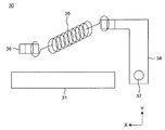
- FIG. 3 is a diagram showing the configuration of the optical module manufacturing apparatus 20 according to the first embodiment.
- the optical module manufacturing apparatus 20 is an apparatus or system for manufacturing an optical module such as the optical module 10 shown in FIGS. 1 and 2.
- the exemplary position accuracy required for the combiner component 13 is ⁇ 10 ⁇ m in the X direction, ⁇ 10 ⁇ m in the Y direction, and ⁇ 50 ⁇ m in the Z direction. Further, the accuracy of the exemplary installation angle required for the combiner component 13 is ⁇ 0.02 degrees in the rotation direction centered on the X axis and ⁇ 0.02 degrees in the rotation direction centered on the Y axis. ..
- the optical module manufacturing apparatus 20 achieves such accuracy.
- the optical module manufacturing device 20 includes a housing positioning device 30 that adjusts the position of the housing 14 of the optical module 10, a component positioning device 24 that adjusts the positions of optical components arranged in the optical module 10, and a position detection unit. 21 and an optical measuring unit 26 are provided.
- the housing positioning device 30 includes a base 31 on which a semi-finished product of the optical module 10 including the housing 14 is placed, and the housing 14 is arranged at a predetermined position.
- the base 31 is an example of the "board" of the present invention.
- the semi-finished product is a product in the process of being manufactured, and in the example shown in FIG. 3, the light source is mounted in the housing 14, but the combiner component 13 is not mounted. Details of the housing positioning device 30 will be described later.
- the component positioning device 24 includes a grip portion 242 for gripping an optical component such as a confluent component 13, a movable stage 25 for moving the grip portion 242, and a load for detecting a force applied to the grip portion 242 in the Y direction. It is provided with a detection unit 241.
- the movable stage 25 can move the grip portion 242 independently in the X, Y, and Z directions, respectively. Further, the movable stage 25 can rotate independently around the X-axis and the Y-axis, respectively.
- the movable stage 25 is, for example, a motor stage driven by a motor.
- the position detection unit 21 detects the positions of the combine wave component 13 and the housing 14.
- the position detection unit 21 is, for example, a position sensor such as an infrared sensor.
- the position detection unit 21 may be an imaging device such as a CCD (Charge Coupled Device) camera or a CMOS (Complementary Metal Oxide Semiconductor) camera.
- the position detection unit 21 is held by the holding unit 231.
- the holding portion 231 is attached to the movable stage 23.
- the movable stage 23 can move the holding portion 231 independently in the X, Y, and Z directions, respectively.
- the movable stage 23 is, for example, a motor stage driven by a motor.
- the light measuring unit 26 includes a laser light source that emits laser light.
- the light measuring unit 26 includes a light measuring unit that irradiates the combiner component 13 with laser light and measures the angle of the laser beam reflected by the combiner component 13.
- the light measuring unit includes, for example, a photodetecting element such as a photodiode.
- the optical modules manufacturing apparatus 20 may include an ultraviolet irradiation unit 22.
- the ultraviolet irradiation unit 22 includes an ultraviolet light source and irradiates ultraviolet rays in a desired direction.
- the ultraviolet irradiation unit 22 irradiates ultraviolet rays from above the combiner component 13 to cure the ultraviolet curable adhesive arranged between the surface of the housing 14 and the combiner component 13.
- the ultraviolet irradiation unit 22 is held by, for example, the irradiation unit holding unit 232 attached to the movable stage 23.
- the operations of the movable stage 25, the movable stage 23, the position detection unit 21, and the optical measurement unit 26 are controlled by an information processing device such as a general-purpose computer equipped with a CPU, for example.
- the housing positioning device 30 positions the housing 14 of the optical module 10.
- the component positioning device 24 grips the confluent component 13 whose bottom surface is coated with the ultraviolet curable adhesive by the grip portion 242.
- the movable stage 25 drives the grip portion 242 to arrange the combine wave component 13 at a predetermined position. Since the wave-combining component 13 is arranged in the housing 14 positioned based on the external shape, the upper portion of the housing 14 is open at the stage of arranging the wave-generating component 13. As described above, the housing 14 is provided with an opening (not shown) at the upper portion.
- the optical module manufacturing apparatus 20 measures the positions of the wave combining component 13 and the housing 14 by the position detecting unit 21.
- the operator drives the movable stage 25 while observing the position measured by the position detection unit 21, and arranges the combine wave component 13 at a predetermined position.
- the drive control of the movable stage 25 may be automatically performed by the information processing device of the optical module manufacturing device 20.
- the position accuracy of the arrangement of the combine wave component 13 depends on, for example, the position resolution of the position detection unit 21 and the lens magnification.
- the positional accuracy of the arrangement of the combiner component 13 achieved by the optical module manufacturing apparatus 20 is ⁇ 5 ⁇ m in the X direction and ⁇ 5 ⁇ m in the Z direction.
- the Y position of the combine wave component 13 is adjusted based on the detection result by the load detection unit 241.
- the load detection unit 241 detects the weight of the combiner component 13.
- the load detected by the load detection unit 241 becomes lighter than the weight of the combiner component 13. Therefore, by monitoring the load by the load detecting unit 241, the wave-matching component 13 can be arranged at a position where the bottom surface of the component 13 comes into contact with the housing 14.
- the operator drives the movable stage 25 and controls the rotation angle ⁇ X around the X-axis and the rotation angle ⁇ Y around the Y-axis of the combiner component 13.
- the light measuring unit 26 irradiates the combiner component 13 with the laser beam and measures the angle of the laser beam reflected from the combiner component 13.
- the operator controls the movable stage 25 so that the values of ⁇ X and ⁇ Y become predetermined values while observing the measurement result.
- the drive control of the movable stage 25 may be automatically performed by the information processing device of the optical module manufacturing device 20.
- the angular accuracy of the arrangement of the combine wave component 13 depends on, for example, the resolution of the optical measuring unit 26.
- the angular accuracy of the arrangement of the combiner component 13 achieved by the optical module manufacturing apparatus 20 is ⁇ 0.005 degrees for the rotation angle ⁇ X around the X axis and ⁇ 0.005 degrees for the rotation angle ⁇ Y around the Y axis. is there.
- ultraviolet rays are irradiated from the ultraviolet irradiation unit 22 toward the combiner component 13, and the ultraviolet rays between the housing 14 and the back surface of the combiner component 13 are emitted.
- the curable adhesive is cured, and the combiner component 13 is adhered to the housing 14.
- the optical module manufacturing apparatus 20 can be applied not only when arranging the combine wave component 13 but also when arranging other optical components arranged in the optical module 10.
- the semi-finished product of the optical module 10 in which the optical components such as the wave wave component 13 are arranged in the housing 14 is completed.
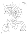
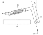
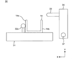
- FIG. 4 is a perspective view showing the structure of the housing positioning device 30 according to the first embodiment.
- the housing positioning device 30 includes a base 31 on which the housing 14 of the optical module 10 is placed.
- a first positioning pin 32a, a second positioning pin 32b, and a third positioning pin 32c for positioning the housing 14 are provided on the base 31.
- the first positioning pin 32a, the second positioning pin 32b, and the third positioning pin 32c are examples of the "support portion" of the present invention.
- the first positioning pin 32a and the second positioning pin 32b are arranged in a straight line in the Z direction.
- the first positioning pin 32a and the second positioning pin 32b come into contact with the first side surface 14a parallel to the YZ plane of the housing 14 to determine the position of the housing 14 in the X direction.
- the housing positioning device 30 further includes a holding portion 34 for pushing the housing 14 toward the first positioning pin 32a and the second positioning pin 32b (that is, in the X direction).
- the pressing portion 34 is arranged in the ⁇ X direction from the arrangement position of the housing 14.
- the pressing portion 34 includes a pressing rod 33 that pushes the housing 14 in contact with a predetermined position of the second side surface 14b facing the first side surface 14a of the housing 14.
- the holding rod 33 has, for example, a cylindrical shape with the X direction as the central axis.
- the third positioning pin 32c is arranged in the + Z direction from the second positioning pin 32b and in the ⁇ X direction from the first positioning pin 32a and the second positioning pin 32b.
- the third positioning pin 32c contacts the third side surface 14c parallel to the XY plane of the housing 14 to determine the position of the housing 14 in the Z direction.
- the housing positioning device 30 further includes a cylindrical rotating shaft 37 extending in the Z direction and a shaft holding portion 38 that rotatably holds the rotating shaft 37 around the Z axis.
- the pressing portion 34 is attached to the rotating shaft 37 and is rotatable about the rotating shaft 37.
- the housing positioning device 30 further includes a lever 39 and an elevating part 40.
- the lever 39 and the elevating part 40 cooperate with each other to adjust the rotation angle of the rotation shaft 37.
- the lever 39 is attached to the rotating shaft 37.
- the lever 39 is an upside-down L-shaped part having a protruding portion 39a protruding in the X direction.
- the elevating portion 40 is a rod-shaped part extending in the X direction having one end 40a and the other end 40b.
- a recess 40c into which the protruding portion 39a of the lever 39 is inserted from the ⁇ X direction is formed at one end 40a of the elevating portion 40.
- the elevating part 40 is provided with an opening (not shown), and the elevating guide 42 is inserted into the opening.
- the lower end of the elevating guide 42 is inserted into the opening 31a provided in the base 31.
- the elevating portion 40 has a screw hole (not shown) on the other end 40b side of the opening into which the elevating guide 42 is inserted, and is fixed to the base 31 by the screw 43. From the above configuration, the mounting position and angle of the lifting portion 40 with respect to the base 31 are determined by the lifting guide 42 and the screw 43.
- the housing positioning device 30 further includes a compression spring 41 in the ⁇ X direction of the opening 31a.
- the elevating part 40 is arranged so as to ride on the compression spring 41.
- the elevating portion 40 may include a spring mounting hole 40d (see FIGS. 7 and 8) into which the compression spring 41 is inserted on the back surface.
- the housing positioning device 30 further includes a support portion 36 arranged on the base 31 and a tension spring 35 having one end attached to the support portion 36. The other end of the tension spring 35 is attached above the rotating shaft 37 of the holding portion 34.
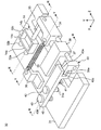
- the operation of the housing positioning device 30 will be described with reference to FIGS. 5 to 10.
- the housing positioning device 30 releases the optical module 10 in a holding state in which the optical module 10 is pressed against the first to third positioning pins 32a to 32c by the pressing portion 34 and held, and the pressing portion 34 is separated from the optical module 10 to release the optical module 10. You can switch between the released state and the released state. In other words, the pressing portion 34 can move between the holding position where the optical module 10 is pressed against the first to third positioning pins 32a to 32c and held, and the release position where the optical module 10 does not come into contact with the optical module 10.
- FIG. 5 is a cross-sectional view of the housing positioning device 30 in the released state as viewed in the VV direction of FIG.
- FIG. 6 is a cross-sectional view of the housing positioning device 30 in the holding state as viewed in the VV direction of FIG.
- FIGS. 5 and 6 are views of a cross section of the pressing portion 34, the tension spring 35, and the supporting portion 36 cut along a plane parallel to the XY plane, as viewed from the ⁇ Z direction.
- FIG. 7 is a cross-sectional view of the housing positioning device 30 in the released state as viewed in the VII-VII direction of FIG.
- FIG. 8 is a cross-sectional view of the housing positioning device 30 in the holding state as viewed in the VII-VII direction of FIG.
- FIGS. 7 and 8 are views of a cross section of the lever 39, the elevating part 40, the compression spring 41, the elevating guide 42, and the screw 43 cut along a plane parallel to the XY plane, as viewed from the ⁇ Z direction. ..
- FIG. 9 is a cross-sectional view of the housing positioning device 30 in the released state and the housing 14 of the optical module 10 as viewed in the IX-IX direction of FIG.
- FIG. 10 is a cross-sectional view of the housing positioning device 30 and the housing 14 of the optical module 10 in the holding state as viewed in the IX-IX direction of FIG.
- FIGS. 9 and 10 show a cross section of the housing positioning device 30 and the housing 14 of the optical module 10 cut along a plane parallel to the XY plane through the center of the first positioning pin 32a in the ⁇ Z direction. It is a figure seen from.
- the tension spring 35 is stretched from the free length and is bridged between the support portion 36 and the holding portion 34 fixed on the base 31. Therefore, in the released state shown in FIG. 5, the pressing portion 34 is pulled in the direction of the supporting portion 36 by the elastic force that the tension spring 35 tries to contract.
- the pressing portion 34 is connected to the lever 39 via the rotating shaft 37 (see FIG. 4), and the lower end of the protruding portion 39a of the lever 39 is in contact with the elevating portion 40 (see FIG. 7). Therefore, the lever 39 and the pressing portion 34 do not move in the direction pulled by the tension spring 35 (that is, they do not rotate counterclockwise about the rotation shaft 37 in FIGS. 5 and 7).
- the housing of the housing 14 does not move and is fixed at a predetermined position.
- the condition that the housing of the housing 14 does not move will be described with reference to FIG.
- the tip of the pressing rod 33 applies a gripping force F1 [N] to the second side surface 14b of the housing 14 at the contact point with the second side surface 14b of the housing 14.
- the gripping force F1 is generated by the force with which the tension spring 35 pulls the pressing portion 34.
- the direction of the gripping force F1 is the rotation direction of the tip of the holding rod 33 about the rotation shaft 37.
- the first side surface 14a of the housing 14 is pressed against the first positioning pin 32a by the gripping force F1, and a drag force F2 [N] is applied to the contact point.
- gravity mg [N] is added to the center of gravity of the housing 14.
- m [kg] is the mass of the housing 14
- g [m / s 2 ] is the gravitational acceleration.
- the gripping force F1, the drag force F2, and the gravity mg as described above are balanced, and the housing 14 does not move.
- the housing positioning device 30 is designed so as to satisfy the condition that the housing 14 does not rotate.
- the conditions are as shown in the following equation (1).
- H [m] includes a contact point between the pressing rod 33 and the second side surface 14b of the housing 14 (that is, a force point of the gripping force F1), the first positioning pin 32a, and the first side surface 14a of the housing 14. Is the distance in the Y direction from the contact point (that is, the force point of the drag force F2).
- M [m] is the distance between the force point of the drag force F2 and the center of gravity of the housing 14 in the X direction.
- W [m] is the distance between the force point of the gripping force F1 and the force point of the drag force F2 in the X direction.
- the gripping force F1 can be adjusted by selecting the spring constant of the tension spring 35 and designing the distance between the support portion 36 and the pressing portion 34 (see FIG. 4). The gripping force F1 is adjusted so as not to cause dents or scratches including dents on the housing 14.
- the housing 14 is positioned in the holding state, the optical components are arranged inside, and then the housing 14 is removed from the housing positioning device 30 by shifting to the released state.
- the elevating portion 40 is raised by the elastic force of the compression spring 41 (see FIGS. 4, 7 and 8).
- the elevating portion 40 rises, the elevating portion 40 comes into contact with the lower end of the protruding portion 39a of the lever 39 and pushes it up.
- the rotating shaft 37 rotates clockwise and returns to the released state shown in FIGS. 5, 7, and 9.
- the optical module manufacturing apparatus 20 of the present embodiment is used for manufacturing the optical module 10 by installing the optical components in the housing 14.
- the optical module manufacturing device 20 includes a housing positioning device 30 that positions the housing 14 of the optical module 10 based on an external shape.
- the housing positioning device 30 includes a base 31 on which the housing 14 is placed, positioning pins 32a, 32b, 32c, and a holding portion 34.
- the positioning pins 32a, 32b, 32c are formed on the base 31 and come into contact with the first side surface 14a of the housing 14 to support the housing 14 at a predetermined position.
- the pressing portion 34 does not come into contact with the housing 14 and the holding position where the housing 14 is pressed against the positioning pins 32a, 32b, 32c in contact with the second side surface 14b facing the first side surface 14a of the housing 14. It is movable between the release position.
- an optical module manufacturing apparatus 20 capable of positioning the housing 14 based on the outer shape is obtained. Since positioning is performed based on the outer shape, the housing 14 can be positioned with high accuracy, and accurate positioning can be repeated. Further, after positioning the housing 14 based on the outer shape, if the mounting position of the optical component relative to the housing 14 is designed, the optical component can be positioned by simply adjusting the position. be able to. For example, the combining component 13 can be positioned only by measuring the angle of the laser beam reflected by the combining component 13 by the light measuring unit 26 without measuring the intensity of the output light of the optical module 10. Therefore, according to the optical module manufacturing apparatus 20, the man-hours and manufacturing time for performing accurate positioning can be reduced.
- the pressing portion 34 comes into contact with the second side surface 14b of the housing at a position higher than the height from the base 31 at the position where the positioning pins 32a, 32b, 32c and the housing 14 are in contact with the positioning pins 32a, 32b, 32c.
- the housing 14 may be pushed by applying a force toward it.
- the first positioning pin 32a and the second positioning pin 32b come into contact with the outer surface of the first side surface 14a of the housing 14 at different positions in the direction in which the first side surface 14a extends to support the housing 14.
- the pressing portion 34 includes a pressing rod 33 that biases the second side surface 14b toward the first side surface 14a so that the line of action of the urging force passes between the first positioning pin 32a and the second positioning pin 32b. You may.
- the housing positioning device 30 of the optical module manufacturing device 20 can be accurately positioned without rotating the housing 14.
- the third positioning pin 32c contacts the outer surface of the third side surface 14c between the first side surface 14a and the second side surface 14b of the housing 14 to support the housing 14.
- the pressing portion 34 may further include a second urging portion that urges the fourth side surface of the housing 14 facing the third side surface 14c toward the third side surface 14c.
- the housing positioning device 30 of the optical module manufacturing device 20 can be accurately positioned without rotating the housing 14.
- the housing 14 may have a quadrangular shape in a plan view.
- the second side surface 14b of the housing 14 is parallel to the first side surface 14a
- the fourth side surface 14d is parallel to the third side surface 14c.
- the housing 14 may be rectangular in a plan view.
- the first positioning pin 32a, the second positioning pin 32b, and the third positioning pin 32c may each have a shape that makes point contact with the housing 14.
- the housing 14 can be positioned with high accuracy.
- the housing 14 is for mounting optical components, and is usually required to have fine dimensions.
- the housing positioning device 30 of the optical module manufacturing device 20 having the above configuration can accurately position the housing 14 having such fine dimensions.
- the pressing portion 34 may be one that presses the housing 14 against the positioning pins 32a, 32b, 32c by using the elastic force of the spring when it is arranged at the holding position.
- the pressing portion 34 transmits the elastic force of the tension spring 35 to press the housing 14 against the positioning pins 32a, 32b, 32c.
- the force for gripping the housing 14 can be adjusted by selecting the spring constant of the tension spring 35.
- the housing 14 having fine dimensions can be accurately positioned.
- the angular accuracy of the positioning of the housing 14 by the housing positioning device 30 is, for example, ⁇ 0.001 degrees with respect to the rotation angle ⁇ X around the X axis, and the rotation around the Y axis.
- the angle ⁇ Y is ⁇ 0.002 degrees.
- the positional accuracy of the arrangement of the wave combining component 13 achieved by the optical module manufacturing apparatus 20 of the present embodiment is ⁇ 5 ⁇ m in the X direction and ⁇ 5 ⁇ m in the Z direction.
- the angular accuracy of the arrangement of the combiner component 13 achieved by the optical module manufacturing apparatus 20 is ⁇ 0.005 degrees for the rotation angle ⁇ X around the X axis and ⁇ 0.005 degrees for the rotation angle ⁇ Y around the Y axis. is there.
- the position accuracy required for the converging component 13 of the optical module 10 is about ⁇ 10 ⁇ m in the X direction, ⁇ 10 ⁇ m in the Y direction, and ⁇ 50 ⁇ m in the Z direction.
- the required angle accuracy is ⁇ 0.02 degrees for the rotation angle ⁇ X around the X axis and ⁇ 0.02 degrees for the rotation angle ⁇ Y around the Y axis. According to the optical module manufacturing apparatus 20 of the present embodiment, these required position accuracy and angle accuracy can be satisfied.
- optical module manufacturing apparatus 20 of the present embodiment it is necessary to use a means for measuring the intensity of the output light from the optical module and searching for the position of the optical component having the maximum or optimum intensity of the output light. Absent. Therefore, an optical module manufacturing apparatus 20 capable of manufacturing an optical module with a small number of procedures and a short time can be obtained.
- the pressing portion 34 that presses the optical module 10 is driven by the elastic force of the tension spring 35 to grip the optical module 10, but the method of gripping the optical module 10 according to the present invention is not limited to this.
- the holding portion may be driven by a cylinder such as an air cylinder or an electric cylinder as described in this embodiment.
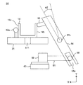
- FIG. 11 is a perspective view showing the structure of the housing positioning device 50 according to the second embodiment of the present invention using a cylinder.
- FIG. 12 is a cross-sectional view of the housing positioning device 50 in the open state as viewed in the XII-XII direction of FIG.
- FIG. 13 is a cross-sectional view of the housing positioning device 50 in the holding state as viewed in the XII-XII direction of FIG.
- FIGS. 12 and 13 are views of a cross section of the housing positioning device 50 and the housing 14 cut along a plane parallel to the XY plane through the center of the first positioning pin 32a, as viewed from the ⁇ Z direction. Is.
- the housing 14 is pressed against the first to third positioning pins 32a to 32c to be positioned.
- the housing positioning device 50 includes a holding portion 54 for pushing the housing 14 toward the first positioning pin 32a and the second positioning pin 32b (that is, in the X direction).
- the pressing portion 54 is arranged in the ⁇ X direction from the arrangement position of the housing 14.
- the pressing portion 54 includes a first pressing rod 53 that pushes the housing 14 in contact with a predetermined position of the second side surface 14b facing the first side surface 14a of the housing 14.
- the first pressing rod 53 has, for example, a cylindrical shape with the X direction as the central axis.
- the housing positioning device 50 further includes a cylindrical rotating shaft 57c extending in the Z direction, and shaft holding portions 57a and 57b that rotatably hold the rotating shaft 57c around the Z axis.
- the pressing portion 54 is attached to the rotating shaft 57 and is rotatable about the rotating shaft 57.
- a groove 54a recessed toward the center of the pressing portion 54 is formed near the lower end of the pressing portion 54.
- the groove 54a extends from one end to the other end of the holding portion 54 in the Z direction.
- a cylindrical guide rod 58 having a central axis in the Z direction is sandwiched in the groove 54a.
- a rod 62 extends from the center of the guide rod 58 in a direction perpendicular to the guide rod 58.
- the rod 62 is attached to the housing positioning device 50 so as to extend in the X direction.
- the pressing portion 54 is formed with an opening or a slit portion (not shown) into which the rod 62 is fitted near the lower end.
- the end of the rod 62 is attached to a rod support 59 that supports the rod 62.
- the rod 62 is a connecting member that connects the rod support portion 59 and the guide rod 58.
- the rod support portion 59 is attached to a first cylinder 60 that can slide in the X direction, and can move in the X direction as the first cylinder 60 operates.
- the housing positioning device 50 includes a second holding rod 55 for pushing the housing 14 toward the third positioning pin 32c (that is, in the Z direction), and a support portion 56 for supporting the second holding rod 55.
- a second cylinder 61 on which the support portion 56 is placed and moved in the Z direction is further provided.
- the second pressing rod 55 is arranged in the ⁇ Z direction from the arrangement position of the housing 14.
- the second pressing rod 53 has, for example, a cylindrical shape with the Z direction as the central axis.
- the first cylinder 60 and the second cylinder 61 include an air cylinder and an electric cylinder.
- the operations of the first cylinder 60 and the second cylinder 61 are controlled by an information processing device such as a general-purpose computer equipped with a CPU, for example.
- the housing positioning device 50 configured as described above will be described.
- the first pressing rod 53 is not in contact with the second side surface 14b of the housing 14.
- the first cylinder 60 is moved in the ⁇ X direction in order to shift from the released state to the holding state.
- the rod support portion 59 on the first cylinder 60, the rod 62 attached to the rod support portion 59, and the guide rod 58 also move in the ⁇ X direction.
- the pressing portion 54 rotates counterclockwise by an angle ⁇ 2 about the rotation shaft 57, and the tip of the first pressing rod 53 comes into contact with the second side surface 14b of the housing 14. To do.
- the gripping force with which the first pressing rod 53 pushes the housing 14 is adjusted by the first cylinder 60.
- the second pressing rod 55 does not come into contact with the fourth side surface 14d of the housing 14 (see FIG. 11).
- the second cylinder 61 is moved in the + Z direction in order to shift from the released state to the holding state.
- the support portion 56 on the second cylinder 61 and the second pressing rod 55 also move in the + Z direction.
- the tip of the second pressing rod 55 comes into contact with the fourth side surface 14d of the housing 14.
- the gripping force with which the second pressing rod 55 pushes the housing 14 is adjusted by the second cylinder 61.
- the housing positioning device 50 shifts to the holding state shown in FIG.
- the housing positioning device 50 may include an opening 511 formed in the substrate 31. In the holding state, the housing 14 is sucked from the lower side of the opening 511 to fix the housing 14 more firmly. You may.
- FIG. 14 is a perspective view showing the structure of the housing positioning device 70 according to the third embodiment of the present invention. Similar to the first and second embodiments, the housing 14 is pressed against the first to third positioning pins 32a to 32c for positioning.
- the housing positioning device 70 includes a first holding rod 73 that pushes the housing 14 toward the first positioning pin 32a and the second positioning pin 32b (that is, in the X direction).
- the first pressing rod 73 has a plunger function and urges the housing 14 to the first positioning pin 32a and the second positioning pin 32b by the elastic force of the spring.
- the first pressing rod 73 is provided with a plunger at the tip.
- the first pressing rod 73 is arranged in the ⁇ X direction from the arrangement position of the housing 14.
- the first pressing rod 53 has, for example, a cylindrical shape with the X direction as the central axis.
- the housing positioning device 70 includes a holding portion 75 for pushing the housing 14 toward the third positioning pin 32c (that is, in the Z direction).
- the pressing portion 75 is arranged in the ⁇ Z direction from the arrangement position of the housing 14.
- the pressing portion 75 includes a second pressing rod 74 that pushes the housing 14 in contact with a predetermined position on the fourth side surface 14d of the housing 14.
- the second pressing rod 74 has a plunger function and urges the housing 14 to the third positioning pin 32c by the elastic force of the spring.
- the second pressing rod 74 is provided with a plunger at the tip.
- the second pressing rod 74 has, for example, a cylindrical shape with the Z direction as the central axis.
- the housing positioning device 70 includes a guide 78 which is a fastener for attaching the pressing portion 75 to the base 31 so as to penetrate the pressing portion 75 in the Y direction and rotate around the Y direction.
- An opening (not shown) penetrating in the Z direction is formed on the opposite side of the pressing portion 75 across the second pressing rod 74.
- a screw 77 is inserted into the opening.
- the screw 77 that penetrates the holding portion 75 in the Z direction is attached to the support portion 79 having a screw hole in the Z direction.
- the holding portion 75 is slidably attached to the supporting portion 79 in the Z direction.
- the pressing portion 75 hardly moves in the X direction and the Y direction with respect to the supporting portion 79.
- the support portion 79 may be integrally formed with the base 31 as shown in FIG. 14, or may be a member attached to the base 31.
- a spring 76 is wound around a portion between the holding portion 75 and the supporting portion 79 of the screw 77.
- the second pressing rod 74 In the released state, the second pressing rod 74 is not in contact with the fourth side surface 14d of the housing 14.
- the screw 77 In order to shift from the released state to the held state, the screw 77 is tightened, and the holding portion 75 is rotated counterclockwise in a plan view around the guide 78.
- the second pressing rod 74 attached to the pressing portion 75 also moves in the direction of approaching the fourth side surface 14d of the housing 14, and eventually comes into contact with the fourth side surface 14d.
- the plunger at the tip of the second pressing rod 74 is pushed in, and the housing 14 is pressed against the third positioning pin 32c.
- the gripping force with which the second pressing rod 74 pushes the housing 14 is adjusted by, for example, the spring constant of the spring in the plunger.
- the operation of the first pressing rod 73 pressing the housing 14 against the first positioning pin 32a and the second positioning pin 32b may be performed by the same mechanism.
- the housing positioning mechanisms of the first to third embodiments may be combined.
- the first holding rod 73 and the second holding rod 74 may be mounted on the cylinder and may be movable with the movement of the cylinder.
- Optical module 11a to 11d light source, 12a to 12d collimator, 13 combined wave parts, 14 housing, 15 mount, 20 optical module manufacturing equipment, 21 position detection unit, 22 ultraviolet irradiation unit, 23 movable stage, 24 equipment, 25 Movable stage, 26 optical measuring unit, 30 device, 31 base (board), 32a to 32c positioning pin (support part), 33 holding rod (first biasing part), 34 holding part, 36 supporting part, 37 rotating shaft, 38 shaft holding part, 39 lever, 40 lifting part, 42 lifting guide, 101 laser light, 131 filter block, 132a to 132c bandpass filter, 133 mirror, 141 opening, 231 holding part, 232 irradiation part holding part, 241 load Detection part, 242 grip part.
Abstract
光学モジュールの筐体(14)内に光学部品を設置して光学モジュールを製造するための光学モジュール製造装置を提供する。光学モジュール製造装置は、筐体を外形基準で位置決めする筐体位置決め装置(30)を備える。筐体位置決め装置は、筐体を載置する基板(31)と、支持部(32a,32b,32c)と、押さえ部(34)と、を備える。支持部は、基板の上に形成され、筐体の第1側面(14a)に接触し、筐体を予め定められた位置で支持する。押さえ部は、筐体の第1側面に対向する第2側面(14b)に接触して支持部に筐体を押し付けて保持する保持位置と、筐体に接触しない解放位置と、の間で移動可能である。
Description
本発明は、光学部品を筐体内に設置して光学モジュールを製造するための光学モジュール製造装置及び光学モジュール製造方法に関する。
光学モジュールを製造するに当たっては、光学モジュールに備えられる光学部品の位置合わせを高精度に行うことが要求される。例えば、特許文献1は、(A)第1のレンズを、第1のレンズの焦点に光源が位置する様に配置する工程と、(B)第2のレンズを、第2のレンズの第1のレンズ側の焦点が第1のレンズの他方の焦点に位置する様に配置する工程と、(C)第3のレンズと光ファイバを模した治具を筐体外面の所定箇所に配置する工程と、(D)第2のレンズを第2のレンズの光軸上を移動して、模した治具の光ファイバに入射する光の強度を所定の値に調整する、光モジュールの製造方法を開示している。この方法により、安定した光出力を得ることができる光モジュールが得られる。
しかしながら、特許文献1に記載の光モジュールの製造方法では、各光学部品は、光モジュールの出力光の強度を計測しながら、強度が所定の値となるように配置される。そのため、光学部品の位置調整の工程数が光学部品の数以上となり、精度の良い位置決めを行うために多大な工数及び製造時間を要する。
本発明の目的は、光学モジュールの位置決めを高精度に行うことができる光学モジュール製造装置及び光学モジュール製造方法を得ることにある。
本発明の一態様は、光学モジュールの筐体内に光学部品を設置して光学モジュールを製造するための光学モジュール製造装置を提供する。光学モジュール製造装置は、筐体を外形基準で位置決めする筐体位置決め装置を備える。筐体位置決め装置は、筐体を載置する基板と、支持部と、押さえ部と、を備える。支持部は、基板の上に形成され、筐体の第1側面に接触し、筐体を予め定められた位置で支持する。押さえ部は、筐体の第1側面に対向する第2側面に接触して支持部に筐体を押し付けて保持する保持位置と、筐体に接触しない解放位置と、の間で移動可能である。
本発明の他の態様は、上記の態様の光学モジュール製造装置を用いて、光学部品を筐体内に設置して光学モジュールを製造するための光学モジュール製造方法を提供する。光学モジュール製造方法は、基板の上に、上部に開口部を備えた筐体を載置し、押さえ部によって支持部に筐体を押し付け、筐体を押し付けた状態で、開口部を介して筐体内に光学部品を配置する。
本発明に係る光学モジュール製造装置及び光学モジュール製造方法によれば、光学モジュールの位置決めを高精度に行うことができる。
以下、本発明の実施の形態に係る光学モジュール製造装置について、図面を参照して説明する。各実施の形態において、同一又は同様の構成には同一の符号を付して、説明を省略する。
実施の形態1.
[光学モジュール]
まず、本発明の実施の形態1に係る製造装置によって製造される光学モジュールの一例として、合波モジュールについて説明する。合波モジュールは、例えば光通信に利用されるモジュールである。
[光学モジュール]
まず、本発明の実施の形態1に係る製造装置によって製造される光学モジュールの一例として、合波モジュールについて説明する。合波モジュールは、例えば光通信に利用されるモジュールである。
光通信に関して、近年、光ネットワークの通信量又はトラフィックが増加している。したがって、光通信分野においては、通信速度が速く、小型で、かつ消費電力の低い光学モジュールが求められる。小型で消費電力の低い光学モジュールを得るために、光学モジュールの集積化が進められている。合波モジュールは、集積化された光学モジュールの一例であり、互いに波長の異なるレーザ光を放射する複数のレーザ装置は、1つの筐体内に配置される。そして、合波モジュールは、これらのレーザ装置から出射されたレーザ光を合波して波長多重レーザ光を出力する。
図1は、光学モジュール10の構成を示す斜視図である。図2は、図1の光学モジュール10の平面図である。図1及び図2には、説明の便宜上、互いに直交するX軸、Y軸及びZ軸を示している。Y軸は鉛直方向の上向きを正方向とし、光学モジュール10から出射されるレーザ光101はZ方向に出射されるものとする。
まず、図2を参照して、光学モジュール10の構成について説明する。光学モジュール10は、レーザ光を出射する4つの光源11a,11b,11c,11dと、各光源にそれぞれ対応する4つのコリメータ12a,12b,12c,12dとを備える。また、光学モジュール10は、各光源から出射されたレーザ光を合波する合波部品13と、筐体14とを更に備える。筐体14は、例えば平面視において矩形であり、矩形の長辺の長さは例えば10mmであり、短辺の長さは例えば6mmである。
光源11a~11dは、同じ高さ(同じY座標)に、X方向に等間隔に配列される。光源11a~11dは、それぞれ、マウント15上に配置されている。マウント15は、例えば放熱機能を有するヒートシンクである。光源11a~11dは、例えば、半導体レーザ素子(レーザダイオード)、固体レーザ素子、又はガスレーザ素子で構成される。光源11a~11dは、例えば、面発光レーザ、端面発光レーザである。光源11aとマウント15との間には、ペルチェ素子が配置されてもよい。光源11b~11dについても同様である。
光源11a~11dは、互いに異なる波長のレーザ光を放射するよう構成される。光源11a,11b,11c,11dから出射されるレーザ光の波長帯域の中心をそれぞれλa,λb,λc,λdとする。λaは例えば1295.5nmである。λbは例えば1300.0nmである。λcは例えば1304.5nmである。λdは例えば1309.0nmである。
図2には、4つの光源11a~11dが示されているが、光源の数は2つ以上であればよく、光学モジュール10の構成はこれに限定されない。
コリメータ12a~12dは、光源11a~11dから出射されたレーザ光を平行化(コリメート)する。各コリメータは、各光源に対応する。すなわち、コリメータ12aには光源11aからのレーザ光100aが入射し、コリメータ12bには光源11bからのレーザ光100bが入射し、コリメータ12cには光源11cからのレーザ光100cが入射し、コリメータ12dには光源11dからのレーザ光100dが入射する。コリメータ12a~12dは、光源11a~11dからZ方向に予め定められた距離を隔てて配置される。
コリメータ12a~12dのそれぞれについて要求される例示的な位置決め精度は、X方向に±0.1μm、Y方向に±0.1μm、Z方向に±1.0μmである。
図2では、各コリメータ12a~12dは別個の光学素子であるように示しているが、これに限定されるものではなく、コリメータ12a~12dの代わりにコリメートレンズアレイが用いられてもよい。また、図2では、コリメータ12a~12dはそれぞれ1つのレンズであるように示しているが、これに限定されるものではなく、複数のレンズで構成されてもよい。
合波部品13は、入射した複数のレーザ光を合波して出力する光学部品である。合波部品13は、フィルタブロック131と、バンドパスフィルタ132a,132b,132cと、ミラー133とを有する。
バンドパスフィルタ132a,132b,132cは、特定の波長帯域の光のみを透過させ、それ以外の波長帯域の光を反射する光学フィルタである。バンドパスフィルタ132aの透過波長帯域は、例えば1293.5nm以上1297.5nm以下である。バンドパスフィルタ132bの透過波長帯域は、例えば1298.0nm以上1302.0nm以下である。バンドパスフィルタ132cの透過波長帯域は、例えば1302.5nm以上1306.5nm以下である。
バンドパスフィルタ132a,132b,132cは、例えば、誘電体多層膜で構成される。バンドパスフィルタ132aは、コリメータ12aにZ方向に隣接して配置され、バンドパスフィルタ132bは、コリメータ12bにZ方向に隣接して配置され、バンドパスフィルタ132cは、コリメータ12cにZ方向に隣接して配置される。したがって、バンドパスフィルタ132aには、光源11aから出射されコリメータ12aを経由したレーザ光100aが入射される。バンドパスフィルタ132bには、光源11bから出射されコリメータ12bを経由したレーザ光100bが入射される。バンドパスフィルタ132cには、光源11cから出射されコリメータ12cを経由したレーザ光100cが入射される。
フィルタブロック131は、ガラス材で構成される。フィルタブロック131は、例えば、平面視において平行四辺形である平行六面体の形状を有する。フィルタブロック131は、直方体の形状を有してもよい。
フィルタブロック131は、バンドパスフィルタ132a,132b,132cに隣接して又は接触して配置される。例えば、バンドパスフィルタ132a,132b,132cは、フィルタブロック131の-Z方向の側面に接着剤を用いて貼り付けられる。
フィルタブロック131には、光源11aから出射され、コリメータ12aを経由し、バンドパスフィルタ132aを透過したレーザ光100aと、光源11bから出射され、コリメータ12bを経由し、バンドパスフィルタ132bを透過したレーザ光100bと、光源11cから出射され、コリメータ12cを経由し、バンドパスフィルタ132cを透過したレーザ光100cと、光源11dから出射され、コリメータ12dを経由したレーザ光100dと、が入射する。
ミラー133は、λbの波長を有する光、λcの波長を有する光、及びλdの波長を有する光を全て反射する。ミラー133は、例えば金等の金属の薄膜又は多層膜を含む。ミラー133は、フィルタブロック131の+Z方向の側面に隣接して又は接触して配置される。例えば、ミラー133は、フィルタブロック131の+Z方向の側面に、金属をコーティングすることよって形成される。
筐体14は、上記の光学部品を収納する。筐体14の+Z側の壁には、壁を貫通する開口部141が形成されている。光学モジュール10の中で合波されることによって形成された波長多重レーザ光101は、開口部141から出射される。上述のマウント15、コリメータ12a~12d、及び合波部品13は、筐体14の底面上に固定される。例えば、合波部品13は、紫外線硬化型接着剤によって筐体14の底面上に接着される。
次に、上記のように構成された光学モジュール10の動作について説明する。
光源11dから出射されたレーザ光100dは、コリメータ12dによって平行化され、フィルタブロック131に入射する。その後、レーザ光100dは、ミラー133とバンドパスフィルタ132c、132b、132aとによって順次反射され、図2に矢印で示した経路を伝播する。
光源11cから出射されたレーザ光100cは、コリメータ12cによって平行化され、バンドパスフィルタ132cを透過して、フィルタブロック131に入射する。その後、レーザ光100cは、ミラー133とバンドパスフィルタ132b、132aとによって順次反射され、図2に矢印で示した経路を伝播する。
光源11bから出射されたレーザ光100bは、コリメータ12bによって平行化され、バンドパスフィルタ132bを透過して、フィルタブロック131に入射する。その後、レーザ光100bは、ミラー133とバンドパスフィルタ132aとによって順次反射され、図2に矢印で示した経路を伝播する。
光源11aから出射されたレーザ光100aは、コリメータ12aによって平行化され、バンドパスフィルタ132aとフィルタブロック131とを透過する。
上記のような経路を伝播したレーザ光100a,100b,100c,100dは、全てフィルタブロック131の出射点Oから+Z方向に出射される。したがって、フィルタブロック131の出射点Oから出射されたレーザ光は、波長λa,λb,λc,λdのレーザ光が合波された波長多重レーザ光101となる。フィルタブロック131の出射点Oから出射された波長多重レーザ光101は、筐体14の開口部141を通って光学モジュール10の外部に出射する。
[光学モジュール製造装置]
特に光通信の分野では、前述のように集積度を増加させるため、光学モジュールの筐体と、その中に配置される光学部品の小型化が要求されている。それに伴い、光学モジュールの組立工程においては、微小領域である筐体内部において合波される光学部品の位置調整及び固定(位置決め)を行うことが課題である。また、従来技術においては、光学部品の位置決め方法として、主に光学モジュールからの出力光の強度を測定し、出力光の強度が最大又は最適となる光学部品の位置を探索する手段が採用されている。しかしながら、この手段では位置調整に長い時間を要することが課題である。
特に光通信の分野では、前述のように集積度を増加させるため、光学モジュールの筐体と、その中に配置される光学部品の小型化が要求されている。それに伴い、光学モジュールの組立工程においては、微小領域である筐体内部において合波される光学部品の位置調整及び固定(位置決め)を行うことが課題である。また、従来技術においては、光学部品の位置決め方法として、主に光学モジュールからの出力光の強度を測定し、出力光の強度が最大又は最適となる光学部品の位置を探索する手段が採用されている。しかしながら、この手段では位置調整に長い時間を要することが課題である。
以下、本発明の実施の形態1に係る光学モジュール製造装置について説明する。図3は、実施の形態1に係る光学モジュール製造装置20の構成を示す図である。光学モジュール製造装置20は、図1及び図2に示した光学モジュール10等の光学モジュールを製造するための装置又はシステムである。
図1及び図2に示したような光学モジュール10を製造する場合、位置に関して高精度で合波部品13を筐体14内に設置する必要がある。具体的には、合波部品13について要求される例示的な位置精度は、X方向に±10μm、Y方向に±10μm、Z方向に±50μmである。また、合波部品13について要求される例示的な設置角度の精度は、X軸を中心とする回転方向について±0.02度、Y軸を中心とする回転方向について±0.02度である。光学モジュール製造装置20は、このような精度を達成する。
光学モジュール製造装置20は、光学モジュール10の筐体14の位置を調整する筐体位置決め装置30と、光学モジュール10内に配置される光学部品の位置を調整する部品位置決め装置24と、位置検出部21と、光測定部26とを備える。
筐体位置決め装置30は、筐体14を含む光学モジュール10の半製品を載置する土台31を備え、筐体14を予め定められた位置に配置する。土台31は、本発明の「基板」の一例である。半製品は、製造途中の製品であり、図3に示した例では、筐体14内に光源が実装されているが、合波部品13が実装されていない状態の製品である。筐体位置決め装置30の詳細については後述する。
部品位置決め装置24は、合波部品13等の光学部品を把持するための把持部242と、把持部242を移動させる可動ステージ25と、把持部242に加えられたY方向の力を検知する荷重検知部241とを備える。可動ステージ25は、把持部242をX、Y及びZ方向にそれぞれ独立に移動させることができる。さらに、可動ステージ25は、X軸周り及びY軸周りにそれぞれ独立に回転可能である。可動ステージ25は、例えばモータによって駆動するモータステージである。
位置検出部21は、合波部品13及び筐体14の位置を検出する。位置検出部21は、例えば、赤外線センサ等の位置センサである。あるいは、位置検出部21は、CCD(Charge Coupled Device)カメラ、CMOS(Complementary Metal Oxide Semiconductor)カメラ等の撮像装置であってもよい。
位置検出部21は、保持部231によって保持される。保持部231は、可動ステージ23に取り付けられている。可動ステージ23は、保持部231をX、Y及びZ方向にそれぞれ独立に移動させることができる。可動ステージ23は、例えばモータによって駆動するモータステージである。
光測定部26は、レーザ光を出射するレーザ光源を含む。光測定部26は、レーザ光を合波部品13に照射し、合波部品13によって反射されたレーザ光の角度を測定する光測定部を備える。光測定部は、例えば、フォトダイオード等の光検知素子を含む。
合波部品13等の光学部品は、位置合わせ完了後、接着剤によって筐体14内に固定される。接着剤は、例えば、紫外線硬化型接着剤である。紫外線硬化型接着剤を用いる場合、光学モジュール製造装置20は、紫外線照射部22を備えてもよい。紫外線照射部22は、紫外光源を含み、所望の方向に紫外線を照射する。紫外線照射部22は、合波部品13の上方から紫外線を照射し、筐体14の表面と合波部品13との間に配置した紫外線硬化型接着剤を硬化させる。紫外線照射部22は、例えば、可動ステージ23に取り付けられた照射部保持部232によって保持される。
可動ステージ25、可動ステージ23、位置検出部21、及び光測定部26の動作は、例えばCPUを備えた汎用コンピュータ等の情報処理装置によって制御される。
以下、上記のように構成された光学モジュール製造装置20による光学モジュール10の製造方法について説明する。
まず、筐体位置決め装置30によって、光学モジュール10の筐体14の位置決めを行う。次に、部品位置決め装置24は、把持部242によって、底面に紫外線硬化型接着剤が塗布された合波部品13を把持する。可動ステージ25は、把持部242を駆動して、合波部品13を予め定められた位置に配置する。外形基準で位置決めされた筐体14の中に合波部品13を配置するため、合波部品13を配置する段階では、筐体14の上部は開いている。このように、筐体14は、上部に開口部(図示せず)を備える。
具体的には、光学モジュール製造装置20は、位置検出部21によって合波部品13及び筐体14の位置を測定する。操作者は、位置検出部21によって測定した位置を見ながら、可動ステージ25を駆動し、合波部品13を予め定められた位置に配置する。あるいは、可動ステージ25の駆動制御は、光学モジュール製造装置20の情報処理装置によって自動的に行われてもよい。
合波部品13の配置の位置精度は、例えば位置検出部21の位置分解能及びレンズ倍率等に依存する。例えば、光学モジュール製造装置20によって達成される合波部品13の配置の位置精度は、X方向に±5μm、Z方向に±5μmである。
合波部品13のY位置の調整は、荷重検知部241による検知結果に基づいて行う。合波部品13が把持部242によって把持され、合波部品13の底面が筐体14に接触していない場合、荷重検知部241は、合波部品13の重さを検知する。合波部品13の底面が筐体14に接触すると、荷重検知部241によって検知される荷重は、合波部品13の重さより軽くなる。したがって、荷重検知部241によって荷重を監視することにより、合波部品13を、その底面が筐体14に接触する位置に配置することができる。
次に、操作者は、可動ステージ25を駆動し、合波部品13のX軸周りの回転角度θX及びY軸周りの回転角度θYを制御する。具体的には、光測定部26は、レーザ光を合波部品13に照射して、合波部品13から反射したレーザ光の角度を測定する。操作者は、測定結果を見ながら、θX及びθYの値が予め定められた値となるように、可動ステージ25を制御する。可動ステージ25の駆動制御は、光学モジュール製造装置20の情報処理装置によって自動的に行われてもよい。
合波部品13の配置の角度精度は、例えば光測定部26の分解能に依存する。例えば、光学モジュール製造装置20によって達成される合波部品13の配置の角度精度は、X軸周りの回転角度θXについて±0.005度、Y軸周りの回転角度θYについて±0.005度である。
上記のようにして合波部品13の位置及び角度を調整した後、紫外線照射部22から合波部品13に向けて紫外線を照射し、筐体14と合波部品13の裏面との間の紫外線硬化型接着剤を硬化させ、合波部品13を筐体14に接着する。
光学モジュール製造装置20は、合波部品13を配置する場合のみならず、光学モジュール10内に配置される他の光学部品を配置する場合にも適用できる。
以上のようにして、筐体14内に合波部品13等の光学部品を配置した光学モジュール10の半製品が完成する。
[筐体位置決め装置]
以下、筐体位置決め装置30の詳細な構造及び動作について説明する。図4は、実施の形態1に係る筐体位置決め装置30の構造を示す斜視図である。
以下、筐体位置決め装置30の詳細な構造及び動作について説明する。図4は、実施の形態1に係る筐体位置決め装置30の構造を示す斜視図である。
筐体位置決め装置30は、光学モジュール10の筐体14を載置する土台31を備える。土台31の上には、筐体14の位置決めのための第1位置決めピン32aと、第2位置決めピン32bと、第3位置決めピン32cとが設けられている。第1位置決めピン32a、第2位置決めピン32b、及び第3位置決めピン32cは、本発明の「支持部」の一例である。
第1位置決めピン32a及び第2位置決めピン32bは、Z方向に一直線に配置されている。第1位置決めピン32a及び第2位置決めピン32bは、筐体14のYZ平面に平行な第1側面14aに接触して筐体14のX方向の位置を決定する。
筐体位置決め装置30は、筐体14を第1位置決めピン32a及び第2位置決めピン32bに向かって(すなわちX方向に)押すための押さえ部34を更に備える。押さえ部34は、筐体14の配置位置より-X方向に配置されている。押さえ部34は、筐体14の第1側面14aに対向する第2側面14bの予め定められた位置に接触して筐体14を押す押さえ棒33を備える。押さえ棒33は、例えばX方向を中心軸とする円柱形状を有する。
第3位置決めピン32cは、第2位置決めピン32bより+Z方向に、かつ、第1位置決めピン32a及び第2位置決めピン32bより-X方向に配置される。第3位置決めピン32cは、筐体14のXY平面に平行な第3側面14cに接触して筐体14のZ方向の位置を決定する。
筐体位置決め装置30は、Z方向に延びた円柱形状の回転軸37と、回転軸37をZ軸周りに回転可能に保持する軸保持部38とを更に備える。押さえ部34は、回転軸37に取り付けられており、回転軸37を中心として回転可能である。
筐体位置決め装置30は、レバー39と昇降部40とを更に備える。レバー39と昇降部40とは、協働して回転軸37の回転角度を調整する。レバー39は、回転軸37に取り付けられている。レバー39は、X方向に突出した突出部39aを備える上下逆さまのL字型のパーツである。昇降部40は、一端40aと他端40bとを備えるX方向に延びた棒状のパーツである。昇降部40の一端40aには、レバー39の突出部39aが-X方向から挿入される凹部40cが形成されている。
昇降部40には図示しない開口部が設けられ、開口部には昇降ガイド42が挿入されている。昇降ガイド42の下端は、土台31に設けられた開口部31aに挿入されている。また、昇降部40は、昇降ガイド42が挿入される開口部より他端40b側に、図示しないねじ穴を有し、ねじ43によって土台31に固定される。以上の構成から、昇降部40は、昇降ガイド42及びねじ43によって、土台31に対する取付位置及び角度が決定される。
筐体位置決め装置30は、開口部31aの-X方向に圧縮ばね41を更に備える。昇降部40は、圧縮ばね41の上に乗るように配置される。昇降部40は、裏面に圧縮ばね41が挿入されるばね取付穴40d(図7及び図8参照)を備えてもよい。
筐体位置決め装置30は、土台31上に配置された支持部36と、一端が支持部36に取り付けられた引張ばね35とを更に備える。引張ばね35の他端は、押さえ部34の回転軸37より上部に取り付けられている。
図5~10を参照して、筐体位置決め装置30の動作について説明する。筐体位置決め装置30は、押さえ部34によって光学モジュール10を第1~第3位置決めピン32a~32cに押し付けて保持する保持状態と、押さえ部34を光学モジュール10から離して光学モジュール10を解放する解放状態と、を切り換えることができる。言い換えれば、押さえ部34は、光学モジュール10を第1~第3位置決めピン32a~32cに押し付けて保持する保持位置と、光学モジュール10に接触しない解放位置と、の間を移動することができる。
図5は、解放状態における筐体位置決め装置30を図4のV-V方向に見た断面図である。図6は、保持状態における筐体位置決め装置30を図4のV-V方向に見た断面図である。言い換えれば、図5及び図6は、押さえ部34と引張ばね35と支持部36とをXY平面に平行な面で切断した断面を、-Z方向から見た図である。
図7は、解放状態における筐体位置決め装置30を図4のVII-VII方向に見た断面図である。図8は、保持状態における筐体位置決め装置30を図4のVII-VII方向に見た断面図である。言い換えれば、図7及び図8は、レバー39、昇降部40、圧縮ばね41、昇降ガイド42、及びねじ43をXY平面に平行な面で切断した断面を、-Z方向から見た図である。
図9は、解放状態における筐体位置決め装置30と光学モジュール10の筐体14とを図4のIX-IX方向に見た断面図である。図10は、保持状態における筐体位置決め装置30と光学モジュール10の筐体14とを図4のIX-IX方向に見た断面図である。言い換えれば、図9及び図10は、筐体位置決め装置30と光学モジュール10の筐体14とを、第1位置決めピン32aの中心を通りXY平面に平行な面で切断した断面を、-Z方向から見た図である。
図5に示すように、引張ばね35は、自由長より引き延ばされた状態で、土台31上に固定された支持部36と押さえ部34とに架け渡されている。したがって、図5に示した解放状態では、押さえ部34は、引張ばね35が縮もうとする弾性力によって支持部36の方向に引っ張られている。しかしながら、押さえ部34はレバー39に回転軸37を介して接続されており(図4参照)、レバー39の突出部39aの下端は昇降部40に接触している(図7参照)。そのため、レバー39及び押さえ部34は、引張ばね35によって引っ張られている方向には動かない(すなわち、図5及び図7において回転軸37を中心に反時計回りに回転しない)。
図7に示した解放状態において、ねじ43を締めて昇降部40を下降させると、保持状態に移行する。なお、ねじ43を締めることにより、昇降部40は、昇降ガイド42の形状に応じて下降する。
昇降部40が下降すると、押さえ部34は、引張ばね35によって引っ張られているため、回転軸37を中心に反時計回りに回転する。このようにして、筐体位置決め装置30は、図6、図8及び図10に示した保持状態に移行する。
図10に示したように、保持状態では、押さえ棒33の先端が筐体14の第2側面14bに接触する。図9に示した解放状態と比較すると、図10の保持状態では、押さえ部34は、回転軸37を中心に角度φ1だけ反時計回りに回転している。なお、図8に示したように、保持状態では、レバー39の突出部39aの下端は昇降部40に接触していない。したがって、解放状態から保持状態への回転軸37の回転は、押さえ棒33の先端が筐体14の第2側面14bに接触したことによって止まっている。
保持状態では、筐体14の筐体は移動せず、予め定められた位置に固定されている。筐体14の筐体が移動しない条件について図10を参照して説明する。
押さえ棒33の先端は、筐体14の第2側面14bとの接触点において、筐体14の第2側面14bに把持力F1[N]を加えている。把持力F1は、引張ばね35が押さえ部34を引っ張る力によって生じている。把持力F1の方向は、回転軸37を中心とする押さえ棒33の先端の回転方向である。把持力F1によって筐体14の第1側面14aが第1位置決めピン32aに押し付けられ、接触点に抗力F2[N]が加わっている。また、筐体14には、重心に重力mg[N]が加わっている。ここで、m[kg]は筐体14の質量であり、g[m/s2]は重力加速度である。以上のような把持力F1、抗力F2、及び重力mgがつり合い、筐体14は移動しない。
また、筐体位置決め装置30は筐体14が回転しない条件を満たすように設計されている。その条件は、次の式(1)の通りである。
(F1cosθ)×H<mg×M+(F1sinθ)×W ・・・(1)
ここで、H[m]は、押さえ棒33と筐体14の第2側面14bとの接触点(すなわち把持力F1の力点)と、第1位置決めピン32aと筐体14の第1側面14aとの接触点(すなわち抗力F2の力点)とのY方向の距離である。M[m]は、抗力F2の力点と筐体14の重心とのX方向の距離である。W[m]は、把持力F1の力点と抗力F2の力点とのX方向の距離である。
(F1cosθ)×H<mg×M+(F1sinθ)×W ・・・(1)
ここで、H[m]は、押さえ棒33と筐体14の第2側面14bとの接触点(すなわち把持力F1の力点)と、第1位置決めピン32aと筐体14の第1側面14aとの接触点(すなわち抗力F2の力点)とのY方向の距離である。M[m]は、抗力F2の力点と筐体14の重心とのX方向の距離である。W[m]は、把持力F1の力点と抗力F2の力点とのX方向の距離である。
なお、把持力F1は、引張ばね35のばね定数の選択や、支持部36と押さえ部34との距離(図4参照)の設計等により調整できる。把持力F1は、筐体14に、凹みを含む打痕や傷を生じさせないように調整される。
上記のように、保持状態において筐体14の位置決めをし、内部に光学部品を配置した後、解放状態に移行させて筐体位置決め装置30から筐体14を取り除く。保持状態から解放状態に移行させるには、ねじ43を緩める。ねじ43を緩めると、圧縮ばね41の弾性力によって、昇降部40が上昇する(図4、図7及び図8参照)。昇降部40が上昇すると、昇降部40がレバー39の突出部39aの下端に接触してこれを押し上げる。これにより回転軸37は時計回りに回転し、図5、図7及び図9に示した解放状態に戻る。
[まとめ]
以上のように、本実施の形態の光学モジュール製造装置20は、光学部品を筐体14内に設置して光学モジュール10を製造するために用いられる。光学モジュール製造装置20は、光学モジュール10の筐体14を外形基準で位置決めする筐体位置決め装置30を備える。筐体位置決め装置30は、筐体14を載置する土台31と、位置決めピン32a,32b,32cと、押さえ部34と、を備える。位置決めピン32a,32b,32cは、土台31の上に形成され、筐体14の第1側面14aに接触し、筐体14を予め定められた位置で支持する。押さえ部34は、筐体14の第1側面14aに対向する第2側面14bに接触して位置決めピン32a,32b,32cに筐体14を押し付けて保持する保持位置と、筐体14に接触しない解放位置と、の間で移動可能である。
以上のように、本実施の形態の光学モジュール製造装置20は、光学部品を筐体14内に設置して光学モジュール10を製造するために用いられる。光学モジュール製造装置20は、光学モジュール10の筐体14を外形基準で位置決めする筐体位置決め装置30を備える。筐体位置決め装置30は、筐体14を載置する土台31と、位置決めピン32a,32b,32cと、押さえ部34と、を備える。位置決めピン32a,32b,32cは、土台31の上に形成され、筐体14の第1側面14aに接触し、筐体14を予め定められた位置で支持する。押さえ部34は、筐体14の第1側面14aに対向する第2側面14bに接触して位置決めピン32a,32b,32cに筐体14を押し付けて保持する保持位置と、筐体14に接触しない解放位置と、の間で移動可能である。
上記の構成により、筐体14を外形基準で位置決めできる光学モジュール製造装置20を得る。外形基準で位置決めするため、筐体14を精度良く位置決めでき、かつ、精度の良い位置決めを繰り返し行うことができる。また、外形基準で筐体14の位置決めを行った後は、光学部品の筐体14に対する相対的な搭載位置が設計されていれば、光学部品については簡易な位置調整を行うだけで位置決めを行うことができる。例えば、光学モジュール10の出力光の強度を計測することなく、光測定部26によって合波部品13によって反射されたレーザ光の角度を測定だけで、合波部品13の位置決めを行うことができる。したがって、光学モジュール製造装置20によれば、精度の良い位置決めを行うための工数及び製造時間を低減できる。
押さえ部34は、位置決めピン32a,32b,32cと筐体14とが接触する位置の土台31からの高さより高い位置で筐体の第2側面14bに接触し、位置決めピン32a,32b,32cに向かう力を加えて筐体14を押してもよい。
第1位置決めピン32a及び第2位置決めピン32bは、筐体14の第1側面14aの外側表面に、第1側面14aが延びる方向に互いに異なる位置でそれぞれ接触して筐体14を支持する。押さえ部34は、付勢力の作用線が第1位置決めピン32aと第2位置決めピン32bとの間を通るように、第2側面14bを第1側面14aに向かって付勢する押さえ棒33を備えてもよい。
上記の構成により、光学モジュール製造装置20の筐体位置決め装置30は、筐体14を回転させることなく、精度良く位置決めすることができる。
第3位置決めピン32cは、筐体14の第1側面14aと第2側面14bとの間の第3側面14cの外側表面に接触して筐体14を支持する。押さえ部34は、筐体14の第3側面14cに対向する第4側面を第3側面14cに向かって付勢する第2付勢部を更に備えてもよい。
上記の構成により、光学モジュール製造装置20の筐体位置決め装置30は、筐体14を回転させることなく、精度良く位置決めすることができる。
筐体14は、平面視において四角形の形状を有してもよい。例えば、筐体14の第2側面14bは第1側面14aに平行であり、第4側面14dは第3側面14cに平行である。筐体14は、平面視において矩形であってもよい。
第1位置決めピン32a、第2位置決めピン32b、及び第3位置決めピン32cは、それぞれ、筐体14と点接触する形状を有してもよい。
上記の構成により、第1位置決めピン32a、第2位置決めピン32b、及び第3位置決めピン32cのそれぞれと、筐体14との接触点の位置を精度良く設計することができる。したがって、筐体14を精度良く位置決めできる。特に、筐体14は、光学部品を搭載するものであり、通常、微細な寸法を有することが要求される。上記の構成の光学モジュール製造装置20の筐体位置決め装置30は、このような微細な寸法を有する筐体14を精度良く位置決めできる。
押さえ部34は、保持位置に配置された場合に、ばねの弾性力を用いて位置決めピン32a,32b,32cに筐体14を押し付けるものであってもよい。例えば、押さえ部34は、引張ばね35の弾性力を伝達して位置決めピン32a,32b,32cに筐体14を押し付ける。
上記の構成により、筐体14を把持する力を、引張ばね35のばね定数を選択することによって調整することができる。これにより、微細な寸法を有する筐体14を精度良く位置決めできる。また、微細な寸法を有する筐体14を破損したり、その表面に傷をつけたりする事態を防止することができる。
本実施の形態の光学モジュール製造装置20によれば、筐体位置決め装置30による筐体14の位置決めの角度精度は、例えばX軸周りの回転角度θXについて±0.001度、Y軸周りの回転角度θYについて±0.002度となる。
また、本実施の形態の光学モジュール製造装置20によって達成される合波部品13の配置の位置精度は、X方向に±5μm、Z方向に±5μmである。さらに、光学モジュール製造装置20によって達成される合波部品13の配置の角度精度は、X軸周りの回転角度θXについて±0.005度、Y軸周りの回転角度θYについて±0.005度である。
例えば、光学モジュール10の合波部品13について要求される位置精度は、X方向に±10μm、Y方向に±10μm、及びZ方向に±50μm程度である。また、要求される角度精度は、X軸周りの回転角度θXについて±0.02度、Y軸周りの回転角度θYについて±0.02度である。本実施の形態の光学モジュール製造装置20によれば、これらの要求される位置精度及び角度精度を満たすことができる。
さらに、本実施の形態の光学モジュール製造装置20によれば、光学モジュールからの出力光の強度を測定し、出力光の強度が最大又は最適となる光学部品の位置を探索する手段を用いる必要がない。したがって、少ない手順及び短時間で光学モジュールを製造できる光学モジュール製造装置20が得られる。
実施の形態2.
実施の形態1では、光学モジュール10を押し付ける押さえ部34は、引張ばね35の弾性力によって駆動されて光学モジュール10を把持したが、本発明による光学モジュール10の把持の方法はこれに限定されない。例えば、押さえ部は、本実施の形態で説明するように、エアシリンダ及び電動シリンダ等のシリンダによって駆動されてもよい。
実施の形態1では、光学モジュール10を押し付ける押さえ部34は、引張ばね35の弾性力によって駆動されて光学モジュール10を把持したが、本発明による光学モジュール10の把持の方法はこれに限定されない。例えば、押さえ部は、本実施の形態で説明するように、エアシリンダ及び電動シリンダ等のシリンダによって駆動されてもよい。
図11は、シリンダを利用する本発明の実施の形態2に係る筐体位置決め装置50の構造を示す斜視図である。図12は、解放状態における筐体位置決め装置50を図11のXII-XII方向に見た断面図である。図13は、保持状態における筐体位置決め装置50を図11のXII-XII方向に見た断面図である。言い換えれば、図12及び図13は、筐体位置決め装置50と筐体14とを、第1位置決めピン32aの中心を通りXY平面に平行な面で切断した断面を、-Z方向から見た図である。
実施の形態1と同様に、筐体14は、第1~第3位置決めピン32a~32cに押し付けられて位置決めされる。筐体位置決め装置50は、筐体14を第1位置決めピン32a及び第2位置決めピン32bに向かって(すなわちX方向に)押すための押さえ部54を備える。押さえ部54は、筐体14の配置位置より-X方向に配置されている。押さえ部54は、筐体14の第1側面14aに対向する第2側面14bの予め定められた位置に接触して筐体14を押す第1押さえ棒53を備える。第1押さえ棒53は、例えばX方向を中心軸とする円柱形状を有する。
筐体位置決め装置50は、Z方向に延びた円柱形状の回転軸57cと、回転軸57cをZ軸周りに回転可能に保持する軸保持部57a、57bとを更に備える。押さえ部54は、回転軸57に取り付けられており、回転軸57を中心として回転可能である。
押さえ部54の下端付近には、押さえ部54の中心に向かって窪んだ溝54aが形成されている。溝54aは、押さえ部54のZ方向の一端から他端にわたって延びている。溝54aには、Z方向を中心軸とする円柱形状のガイド棒58が挟み込まれている。ガイド棒58の中央からは、ガイド棒58に垂直な方向にロッド62が延びている。ロッド62は、X方向に延びるように筐体位置決め装置50に取り付けられる。押さえ部54には、下端付近に、ロッド62が嵌め込まれる図示しない開口部又はスリット部が形成されている。ロッド62の端部は、ロッド62を支持するロッド支持部59に取り付けられている。ロッド62は、ロッド支持部59とガイド棒58とを連結する連結部材である。ロッド支持部59は、X方向にスライド可能な第1シリンダ60に取り付けられ、第1シリンダ60の動作に伴ってX方向に移動可能である。
また、筐体位置決め装置50は、筐体14を第3位置決めピン32cに向かって(すなわちZ方向に)押すための第2押さえ棒55と、第2押さえ棒55を支持する支持部56と、支持部56を載置してZ方向に移動させる第2シリンダ61とを更に備える。第2押さえ棒55は、筐体14の配置位置より-Z方向に配置されている。第2押さえ棒53は、例えばZ方向を中心軸とする円柱形状を有する。
第1シリンダ60及び第2シリンダ61は、エアシリンダ及び電動シリンダを含む。第1シリンダ60及び第2シリンダ61の動作は、例えばCPUを備えた汎用コンピュータ等の情報処理装置によって制御される。
上記のように構成された筐体位置決め装置50の動作について説明する。図12に示した解放状態では、第1押さえ棒53は、筐体14の第2側面14bに接触していない。解放状態から保持状態に移行するために、第1シリンダ60を-X方向に移動させる。これにより、第1シリンダ60上のロッド支持部59、ロッド支持部59に取り付けられたロッド62及びガイド棒58も-X方向に移動する。これにより、図13に示したように、押さえ部54が回転軸57を中心として反時計回りに角度φ2だけ回転し、第1押さえ棒53の先端が、筐体14の第2側面14bに接触する。第1押さえ棒53が筐体14を押す把持力は、第1シリンダ60によって調整される。
また、解放状態では、第2押さえ棒55は、筐体14の第4側面14dに接触しない(図11参照)。解放状態から保持状態に移行するために、第2シリンダ61を+Z方向に移動させる。これにより、第2シリンダ61上の支持部56及び第2押さえ棒55も+Z方向に移動する。これにより、第2押さえ棒55の先端が、筐体14の第4側面14dに接触する。第2押さえ棒55が筐体14を押す把持力は、第2シリンダ61によって調整される。
このようにして、筐体位置決め装置50は、図12に示した保持状態に移行する。なお、筐体位置決め装置50は、基板31に形成された開口部511を備えてもよく、保持状態において、開口部511の下側から筐体14を吸引し、筐体14をより強固に固定してもよい。
実施の形態3.
図14は、本発明の実施の形態3に係る筐体位置決め装置70の構造を示す斜視図である。実施の形態1及び2と同様に、筐体14は、第1~第3位置決めピン32a~32cに押し付けられて位置決めされる。
図14は、本発明の実施の形態3に係る筐体位置決め装置70の構造を示す斜視図である。実施の形態1及び2と同様に、筐体14は、第1~第3位置決めピン32a~32cに押し付けられて位置決めされる。
筐体位置決め装置70は、筐体14を第1位置決めピン32a及び第2位置決めピン32bに向かって(すなわちX方向に)押す第1押さえ棒73を備える。第1押さえ棒73は、プランジャ機能を有し、ばねの弾性力によって、筐体14を第1位置決めピン32a及び第2位置決めピン32bに付勢する。あるいは、第1押さえ棒73は、先端にプランジャを備える。第1押さえ棒73は、筐体14の配置位置より-X方向に配置されている。第1押さえ棒53は、例えばX方向を中心軸とする円柱形状を有する。
筐体位置決め装置70は、筐体14を第3位置決めピン32cに向かって(すなわちZ方向に)押すための押さえ部75を備える。押さえ部75は、筐体14の配置位置より-Z方向に配置されている。押さえ部75は、筐体14の第4側面14dの予め定められた位置に接触して筐体14を押す第2押さえ棒74を備える。第2押さえ棒74は、プランジャ機能を有し、ばねの弾性力によって、筐体14を第3位置決めピン32cに付勢する。あるいは、第2押さえ棒74は、先端にプランジャを備える。第2押さえ棒74は、例えばZ方向を中心軸とする円柱形状を有する。
筐体位置決め装置70は、押さえ部75をY方向に貫通して、Y方向を中心に回転可能に押さえ部75を土台31に取り付ける締結具であるガイド78を備える。押さえ部75の、第2押さえ棒74を挟んで反対側には、Z方向に貫通した開口部(図示せず)が形成されている。開口部には、ねじ77が挿入される。押さえ部75をZ方向に貫通したねじ77は、Z方向のねじ穴を有する支持部79に取り付けられる。これにより、押さえ部75は、支持部79に対してZ方向にスライド可能に取り付けられる。押さえ部75は、支持部79に対してX方向及びY方向にはほとんど動かない。
支持部79は、図14に示すように土台31と一体的に形成されてもよいし、土台31に取り付けられる部材であってもよい。
ねじ77の押さえ部75と支持部79との間の部分には、ばね76が巻き付けられている。
上記のように構成された筐体位置決め装置70の動作について説明する。解放状態では、第2押さえ棒74は、筐体14の第4側面14dに接触していない。解放状態から保持状態に移行するために、ねじ77を締め、ガイド78を中心に押さえ部75を平面視において反時計回りに回転させる。これにより、押さえ部75に取り付けられた第2押さえ棒74も筐体14の第4側面14dに近付く方向に移動し、やがて第4側面14dに接触する。さらにねじ77を締めると、第2押さえ棒74の先端のプランジャが押し込まれて、筐体14が第3位置決めピン32cに押し付けられる。第2押さえ棒74が筐体14を押す把持力は、例えばプランジャ内のばねのばね定数によって調整される。
第1押さえ棒73が筐体14を第1位置決めピン32a及び第2位置決めピン32bに押し付ける動作も、同様の機構によって行われてもよい。
実施の形態1~3の筐体位置決め機構は、組み合わされてもよい。例えば、第1押さえ棒73及び第2押さえ棒74は、シリンダの上に取り付けられて、シリンダの移動に伴って移動可能であってもよい。
10 光学モジュール、11a~11d 光源、12a~12d コリメータ、13 合波部品、14 筐体、15 マウント、20 光学モジュール製造装置、21 位置検出部、22 紫外線照射部、23 可動ステージ、24 装置、25 可動ステージ、26 光測定部、30 装置、31 土台(基板)、32a~32c 位置決めピン(支持部)、33 押さえ棒(第1付勢部)、34 押さえ部、36 支持部、37 回転軸、38 軸保持部、39 レバー、40 昇降部、42 昇降ガイド、101 レーザ光、131 フィルタブロック、132a~132c バンドパスフィルタ、133 ミラー、141 開口部、231 保持部、232 照射部保持部、241 荷重検知部、242 把持部。
Claims (9)
- 光学モジュールの筐体内に光学部品を設置して前記光学モジュールを製造するための光学モジュール製造装置であって、
前記筐体を外形基準で位置決めする筐体位置決め装置を備え、
前記筐体位置決め装置は、
前記筐体を載置する基板と、
前記基板の上に形成され、前記筐体の第1側面に接触し、前記筐体を予め定められた位置で支持する支持部と、
前記筐体の前記第1側面に対向する第2側面に接触して前記支持部に前記筐体を押し付けて保持する保持位置と、前記筐体に接触しない解放位置と、の間で移動可能な押さえ部と、を備える、
光学モジュール製造装置。 - 前記押さえ部は、前記支持部と前記筐体とが接触する位置の前記基板からの高さより高い位置で前記筐体の前記第2側面に接触し、前記支持部に向かう力を加えて前記筐体を押す、請求項1に記載の光学モジュール製造装置。
- 前記支持部は、前記筐体の前記第1側面の外側表面に、前記第1側面が延びる方向に互いに異なる位置でそれぞれ接触して前記筐体を支持する第1位置決めピン及び第2位置決めピンを備え、
前記押さえ部は、付勢力の作用線が前記第1位置決めピンと前記第2位置決めピンとの間を通るように、前記第2側面を前記第1側面に向かって付勢する第1付勢部を備える、
請求項1又は2のいずれかに記載の光学モジュール製造装置。 - 前記支持部は、前記筐体の前記第1側面と前記第2側面との間の第3側面の外側表面に接触して前記筐体を支持する第3位置決めピンを更に備え、
前記押さえ部は、前記筐体の前記第3側面に対向する第4側面を前記第3側面に向かって付勢する第2付勢部を更に備える、
請求項1~3のいずれかに記載の光学モジュール製造装置。 - 前記筐体は、平面視において四角形の形状を有し、前記第2側面は前記第1側面に平行であり、前記第4側面は前記第3側面に平行である、請求項4に記載の光学モジュール製造装置。
- 前記支持部は、前記筐体と点接触する形状を有する、請求項1~5のいずれかに記載の光学モジュール製造装置。
- 前記押さえ部は、前記保持位置に配置された場合に、ばねの弾性力を用いて前記支持部に前記筐体を押し付ける、請求項1~6のいずれかに記載の光学モジュール製造装置。
- 前記筐体は上部に開口部を備え、前記開口部を介して前記筐体内に前記光学部品を設置する請求項1~7のいずれかに記載の光学モジュール製造装置であって、
前記筐体の前記開口部を介して前記光学部品の位置を検出する位置検出部と、
前記光学部品に光を照射し、その反射光の角度を測定する光測定部と、
前記光学部品を把持し、前記筐体の前記開口部から前記筐体の中に入り、前記筐体内における前記光学部品の位置を調整する部品位置決め装置と、
を更に備える、光学モジュール製造装置。 - 請求項1~8のいずれかに記載の光学モジュール製造装置を用いて、前記光学部品を前記筐体内に設置して前記光学モジュールを製造するための光学モジュール製造方法であって、
前記基板の上に、上部に開口部を備えた前記筐体を載置し、
前記押さえ部によって前記支持部に前記筐体を押し付け、
前記筐体を押し付けた状態で、前記開口部を介して前記筐体内に前記光学部品を配置する、
光学モジュール製造方法。
Priority Applications (1)
| Application Number | Priority Date | Filing Date | Title |
|---|---|---|---|
| JP2021518343A JPWO2020226065A1 (ja) | 2019-05-07 | 2020-04-23 | 光学モジュール製造装置及び光学モジュール製造方法 |
Applications Claiming Priority (2)
| Application Number | Priority Date | Filing Date | Title |
|---|---|---|---|
| JP2019087672 | 2019-05-07 | ||
| JP2019-087672 | 2019-05-07 |
Publications (1)
| Publication Number | Publication Date |
|---|---|
| WO2020226065A1 true WO2020226065A1 (ja) | 2020-11-12 |
Family
ID=73051094
Family Applications (1)
| Application Number | Title | Priority Date | Filing Date |
|---|---|---|---|
| PCT/JP2020/017482 WO2020226065A1 (ja) | 2019-05-07 | 2020-04-23 | 光学モジュール製造装置及び光学モジュール製造方法 |
Country Status (2)
| Country | Link |
|---|---|
| JP (1) | JPWO2020226065A1 (ja) |
| WO (1) | WO2020226065A1 (ja) |
Citations (7)
| Publication number | Priority date | Publication date | Assignee | Title |
|---|---|---|---|---|
| JPH0243072U (ja) * | 1988-09-17 | 1990-03-26 | ||
| JPH0919834A (ja) * | 1995-07-10 | 1997-01-21 | Fujitsu Ten Ltd | 組立ロボット用ワ−ク位置決め装置 |
| JP2004205545A (ja) * | 2002-12-20 | 2004-07-22 | Ricoh Co Ltd | 光束特性変換素子の実装装置及び実装方法 |
| WO2008087725A1 (ja) * | 2007-01-18 | 2008-07-24 | Advantest Corporation | 基板固定装置及び基板固定方法 |
| JP2010093168A (ja) * | 2008-10-10 | 2010-04-22 | Nec Corp | 光モジュール製造装置、製造装置システム、製造方向、および製造処理プログラム |
| JP2015043028A (ja) * | 2013-08-26 | 2015-03-05 | 三菱電機株式会社 | 集積型光モジュールの製造装置および製造方法 |
| JP2016045237A (ja) * | 2014-08-20 | 2016-04-04 | 住友電気工業株式会社 | 発光モジュール及び多チャネル発光モジュール |
Family Cites Families (1)
| Publication number | Priority date | Publication date | Assignee | Title |
|---|---|---|---|---|
| JP6865658B2 (ja) * | 2017-09-07 | 2021-04-28 | 三菱電機株式会社 | 光モジュールの製造方法および製造装置 |
-
2020
- 2020-04-23 WO PCT/JP2020/017482 patent/WO2020226065A1/ja active Application Filing
- 2020-04-23 JP JP2021518343A patent/JPWO2020226065A1/ja active Pending
Patent Citations (7)
| Publication number | Priority date | Publication date | Assignee | Title |
|---|---|---|---|---|
| JPH0243072U (ja) * | 1988-09-17 | 1990-03-26 | ||
| JPH0919834A (ja) * | 1995-07-10 | 1997-01-21 | Fujitsu Ten Ltd | 組立ロボット用ワ−ク位置決め装置 |
| JP2004205545A (ja) * | 2002-12-20 | 2004-07-22 | Ricoh Co Ltd | 光束特性変換素子の実装装置及び実装方法 |
| WO2008087725A1 (ja) * | 2007-01-18 | 2008-07-24 | Advantest Corporation | 基板固定装置及び基板固定方法 |
| JP2010093168A (ja) * | 2008-10-10 | 2010-04-22 | Nec Corp | 光モジュール製造装置、製造装置システム、製造方向、および製造処理プログラム |
| JP2015043028A (ja) * | 2013-08-26 | 2015-03-05 | 三菱電機株式会社 | 集積型光モジュールの製造装置および製造方法 |
| JP2016045237A (ja) * | 2014-08-20 | 2016-04-04 | 住友電気工業株式会社 | 発光モジュール及び多チャネル発光モジュール |
Also Published As
| Publication number | Publication date |
|---|---|
| JPWO2020226065A1 (ja) | 2021-10-14 |
Similar Documents
| Publication | Publication Date | Title |
|---|---|---|
| EP2795674B1 (en) | Opto-electronic modules, in particular flash modules, and method for manufacturing the same | |
| CN109073844B (zh) | 光学子组件与光电器件的光学对准 | |
| JP7020039B2 (ja) | 光受信モジュールの製造方法 | |
| JP4143067B2 (ja) | 複数の光学素子を1つの単一基板上へ同時精密ダイ接着を行うためのシステムおよび方法 | |
| CN110308564B (zh) | 光合波器的制造装置 | |
| JP2004354176A (ja) | 光検出器及びそれを用いた分光器 | |
| JP2004086136A (ja) | 光トランシーバの製造方法及び調整装置 | |
| JP2003255166A (ja) | 立体光導波路、その製造方法、光モジュール、および光伝送システム | |
| US10788632B2 (en) | Device and method for coupling laser to a photonic integrated circuit | |
| WO2020226065A1 (ja) | 光学モジュール製造装置及び光学モジュール製造方法 | |
| US8646958B2 (en) | Light emitting device | |
| WO2012042944A1 (ja) | 光学式変位センサの調整方法、および光学式変位センサの製造方法 | |
| US11303357B1 (en) | Systems, methods, and devices for optical assemblies | |
| JP6865658B2 (ja) | 光モジュールの製造方法および製造装置 | |
| JP2021149075A (ja) | 光学モジュールの製造方法、および光学モジュールの製造装置 | |
| JP5004412B2 (ja) | レンズ一体型撮像装置の製造方法及び製造装置 | |
| JP2019186472A (ja) | 光学装置の製造装置および光学装置の製造方法 | |
| JP2020012953A (ja) | レンズユニット、レンズユニットの組立方法、対象物検出装置 | |
| JP2011170271A (ja) | 光学装置、光学部品の位置調整固定方法、及びレーザプロジェクタ | |
| JP2014240958A (ja) | 光モジュール | |
| JP2019203926A (ja) | 接続装置 | |
| JP7050480B2 (ja) | 光モジュールの製造方法及び光モジュール製造装置 | |
| KR20170000936A (ko) | 분광 측정 장치의 측정 헤드 정렬 장치 | |
| JP2005010334A (ja) | 複合光学素子および複合光学部品および複合光学素子の製造方法 | |
| JP2023114378A (ja) | 検査装置及び検査方法 |
Legal Events
| Date | Code | Title | Description |
|---|---|---|---|
| 121 | Ep: the epo has been informed by wipo that ep was designated in this application |
Ref document number: 20801916 Country of ref document: EP Kind code of ref document: A1 |
|
| ENP | Entry into the national phase |
Ref document number: 2021518343 Country of ref document: JP Kind code of ref document: A |
|
| NENP | Non-entry into the national phase |
Ref country code: DE |
|
| 122 | Ep: pct application non-entry in european phase |
Ref document number: 20801916 Country of ref document: EP Kind code of ref document: A1 |