WO2020196009A1 - 時間計測回路 - Google Patents
時間計測回路 Download PDFInfo
- Publication number
- WO2020196009A1 WO2020196009A1 PCT/JP2020/011377 JP2020011377W WO2020196009A1 WO 2020196009 A1 WO2020196009 A1 WO 2020196009A1 JP 2020011377 W JP2020011377 W JP 2020011377W WO 2020196009 A1 WO2020196009 A1 WO 2020196009A1
- Authority
- WO
- WIPO (PCT)
- Prior art keywords
- clock
- circuit
- phase
- counter
- stop signal
- Prior art date
- Legal status (The legal status is an assumption and is not a legal conclusion. Google has not performed a legal analysis and makes no representation as to the accuracy of the status listed.)
- Ceased
Links
Images









Classifications
-
- G—PHYSICS
- G04—HOROLOGY
- G04F—TIME-INTERVAL MEASURING
- G04F10/00—Apparatus for measuring unknown time intervals by electric means
- G04F10/04—Apparatus for measuring unknown time intervals by electric means by counting pulses or half-cycles of an AC
Definitions
- the present invention relates to a time measurement circuit capable of performing highly accurate time measurement.
- TDC Time-to-Digital Converter
- PLL Delay Locked Loop
- PLL Phase Locked Loop
- ultrasonic flowmeters for gas meters need to measure the ultrasonic propagation time difference with low power consumption, high accuracy, and high resolution, so the operating period of the high-speed counter (high-speed clock oscillation period) must be as short as possible.
- the DLL type TDC and the PLL type TDC require time to stabilize the oscillation of the delay circuit, so that the oscillation period of the high-speed clock becomes long, which is disadvantageous in terms of power consumption.
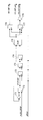
- FIG. 25 is a circuit diagram showing the configuration of a conventional ring oscillator type TDC.
- the ring oscillator type TDC is composed of a D flip-flop circuit 10, a ring oscillator 11, and a high-speed counter 12.
- the D flip-flop circuit 10 uses the 1-bit binary number “1” (1'b1) as the D input, the oscillation start signal ROSC_START as the clock input, the oscillation stop signal ROSC_STOP as the reset input, and outputs the oscillation permission signal TDC_EN. ..
- the ring oscillator 11 generates a high-speed clock TAP [2] during the period when the oscillation permission signal TDC_EN is significant.
- the high speed counter 12 counts the high speed clock.
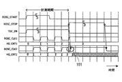
- FIG. 26 is a timing chart illustrating the operation of the ring oscillator type TDC of FIG. 25.
- the D flip flop circuit 10 uses the 1-bit binary number “1” (1'b1) as the D input, the oscillation start signal ROSC_START as the clock input, and the oscillation stop signal ROSC_STOP as the reset input, and oscillates as shown in FIG.
- the oscillation permission signal TDC_EN which becomes significant at the rising edge of the start signal ROSC_START and becomes unintentional (Low) at the rising edge of the oscillation stop signal ROSC_STOP, is output.
- the ring oscillator 11 includes a NAND circuit 110 that takes a negative logical product of the oscillation permission signal TDC_EN and the high-speed clock TAP [2], a buffer circuit 111-1 that inputs the output TAP [0] of the NAND circuit 110, and a buffer circuit. It is composed of a buffer circuit 111-2 that takes the output TAP [1] of 111-1 as an input and outputs the output TAP [2] as a high-speed clock. As shown in FIG. 26, the ring oscillator 11 generates a clock TAP [2] faster than the low-speed clock (ROSC_STOP) during the period when the oscillation permission signal TDC_EN output from the D flip-flop circuit 10 is significant.
- the high-speed counter 12 counts the rising edge of the high-speed clock TAP [2] and outputs the counting result HS_CNT.
- the present invention has been made to solve the above problems, and an object of the present invention is to provide a time measurement circuit capable of realizing low power consumption operation and accurate time measurement.
- the time measurement circuit (first embodiment) of the present invention is configured to output an oscillation permission signal that becomes significant at the timing of input of a start signal from the outside and becomes unintentional at the timing of input of a stop signal from the outside.
- the flip-flop circuit, the oscillation circuit configured to generate the first clock during the period in which the oscillation permission signal is significant, the first clock, and the first clock inverted.
- a logic circuit configured to mask each of the two clocks with the stop signal, a first counter configured to count the first clock masked with the stop signal, and masking with the stop signal.
- the second counter configured to count the second clock and the count results of the first and second counters, the counter in which the clock input having an unacceptable time width is not generated.
- a selector configured to select the counting result obtained by, and a time interval from the input of the start signal to the input of the stop signal based on the counting result selected by the selector after the input of the stop signal. It is characterized by including a time calculation unit configured to calculate.
- the selector is the first counter in the range where the phase of the first clock is smaller than 0 ° to 180 ° and less than a predetermined first phase value.
- the counting result of the second counter is selected, and in the range where the phase of the first clock is 180 ° or more and less than 360 ° from the first phase value and less than a predetermined second phase value, the counting result of the second counter is selected. Is selected, and the counting result of the first counter is selected in the range where the phase of the first clock is equal to or more than the second phase value and less than 360 °.
- the logic circuit uses a buffer circuit for which the first clock output from the oscillation circuit is input and a first clock output from the oscillation circuit.
- An inverter configured to generate the inverted second clock
- a first OR circuit configured to OR mask the first clock output from the buffer circuit with the stop signal. It is characterized in that it is composed of a second OR circuit configured to OR-mask the second clock output from the inverter with the stop signal.
- the time measurement circuit (second embodiment) of the present invention becomes significant at the timing of input of the start signal from the outside, and outputs an unexpected oscillation permission signal at the timing of input of the stop signal from the outside.
- a flip flop circuit configured in, an oscillation circuit configured so that the oscillation permission signal generates a first clock during a significant period, and a second clock in which the first clock is masked by the stop signal.
- a logic circuit configured to generate a clock, a first counter configured to count the first clock, a second counter configured to count the second clock, and the above.
- a selector configured to select the counting result obtained by the counter that does not generate an unacceptable time width clock input among the counting results of the first and second counters, and the stop signal. It is characterized by including a time calculation unit configured to calculate the time interval from the input of the start signal to the input of the stop signal based on the counting result selected by the selector after the input of. is there.
- the selector is the second counter in the range where the phase of the first clock is smaller than 0 ° to 180 ° and less than a predetermined first phase value.
- the counting result of the first counter is selected, and the counting result of the first counter is in the range where the phase of the first clock is 180 ° or more and less than 360 ° from the first phase value and less than a predetermined second phase value.
- the counting result of the second counter is selected in the range where the phase of the first clock is equal to or more than the second phase value and less than 360 °.
- the logic circuit is configured to generate the second clock obtained by OR-masking the first clock output from the oscillation circuit with the stop signal. It is characterized in that it is composed of an OR circuit.
- the time measurement circuit (third embodiment) of the present invention includes a test execution unit configured to test the time measurement circuit, a first start signal input from the outside at normal times, and a first first.
- the stop signal is selected and output
- the second start signal and the second stop signal output from the test execution unit are selected and output at the time of test execution
- the third stop signal is output at the end of the test. It becomes significant at the input timing of the first start signal or the second start signal with the operation setting circuit configured as described above, and is unintentional at the input timing of the first stop signal or the third stop signal.
- a flip-flop circuit configured to output an oscillation permit signal, an oscillation circuit configured to generate a first clock during a significant period of the oscillation permit signal, and the first clock.
- a logic circuit configured to mask the second clock obtained by inverting the first clock with the first stop signal or the second stop signal, respectively, and the first stop signal or the second stop signal.
- a first counter configured to count the first clock masked by the second stop signal and a second clock masked by the first stop signal or the second stop signal. Select the counting result obtained by the second counter configured in the above and the counting result of the first and second counters, whichever has no clock input having an unacceptable time width.
- the time from the input of the first start signal to the input of the first stop signal based on the selector configured as described above and the counting result selected by the selector after the input of the first stop signal in normal times.
- the test execution unit includes a time calculation unit configured to calculate the interval, and the test execution unit tests the oscillation circuit by comparing the count results of the first and second counters at the time of test execution. It is characterized by.
- the selector is the first counter in the range where the phase of the first clock is smaller than 0 ° to 180 ° and less than a predetermined first phase value.
- the counting result of the second counter is selected, and in the range where the phase of the first clock is 180 ° or more and less than 360 ° from the first phase value and less than a predetermined second phase value, the counting result of the second counter is selected. Is selected, and the counting result of the first counter is selected in the range where the phase of the first clock is equal to or more than the second phase value and less than 360 °.
- the test execution unit when the phase of the first clock is a value immediately before the first phase value and when the phase of the first phase value is the first phase value, the test execution unit Alternatively, the counting result of the first counter and the counting result of the second counter when the value is immediately after the first phase value are acquired and compared, and the phase of the first clock is the first.
- the test execution unit causes the oscillation when the acquired count result of the first counter and the count result of the second counter match. It is characterized in that it is determined that the oscillation circuit is out of order when it is determined that the circuit is normal and the counting result of the first counter and the counting result of the second counter do not match. ..
- the test execution unit determines.
- the counting result of the first counter and the counting result of the second counter when the value is immediately after the first phase value are acquired, the counting result of the acquired second counter is subtracted by 1. After that, the counting result of the first counter and the counting result of the second counter are compared.
- the logic circuit uses a buffer circuit for inputting the first clock output from the oscillation circuit and a first clock output from the oscillation circuit.
- An inverter configured to generate the inverted second clock, and mask the first clock later than the second clock and mask it later than the second clock when the test is executed.
- the mask release timing control circuit configured to be generated from the second stop signal and the first clock output from the buffer circuit are OR-masked with the first stop signal or the fourth stop signal.
- the first OR circuit configured as described above and the second OR circuit configured to OR-mask the second clock output from the inverter with the first stop signal or the fifth stop signal.
- the oscillation circuit, the buffer circuit, and the inverter operate so that when the oscillation permission signal becomes significant, the second clock becomes significant before the first clock. It is characterized by doing.
- the time calculation unit is a count selected by the selector when the phase of the first clock is in the range of the first phase value or more and less than 360 °. When the result is taken in, the counting result is subtracted by 1 and then the time interval is calculated.
- an encoder that outputs a signal indicating the phase value of the output of the oscillation circuit is further provided, and the selector is based on the signal output from the encoder. It is characterized in that one of the counting results of the first and second counters is selected.
- a logic circuit that masks a first clock generated by an oscillation circuit and a second clock that inverts the first clock with a stop signal, and a first masked with a stop signal.
- the clock input having an unacceptable time width.
- a logic circuit for generating a second clock in which the first clock generated by the oscillation circuit is masked with a stop signal, a first counter for counting the first clock, and a second clock are used.
- a second counter for counting and a selector for selecting the counting result obtained by the counter that does not generate the clock input having an unacceptable time width among the counting results of the first and second counters are provided.
- a logic circuit that masks the first clock generated by the oscillation circuit and the second clock obtained by inverting the first clock with the first stop signal or the second stop signal, respectively.
- a first counter that counts the first clock masked by the first stop signal or the second stop signal
- a second clock that counts the second clock masked by the first stop signal or the second stop signal.
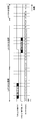
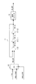
- FIG. 1 is a circuit diagram showing a configuration of a time measurement circuit according to a first embodiment of the present invention.
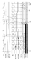
- FIG. 2 is a timing chart illustrating the operation of the time measurement circuit according to the first embodiment of the present invention.
- FIG. 3 is a circuit diagram showing a configuration of an edge detection circuit of the time measurement circuit according to the first embodiment of the present invention.
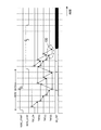
- FIG. 4 is a diagram showing the relationship between the high-speed clock and the timing signal in the first embodiment of the present invention.
- FIG. 5 is a timing chart illustrating a method for correcting the counting result of the high-speed clock according to the first embodiment of the present invention.
- FIG. 6 is a timing chart illustrating a method for correcting the counting result of the high-speed clock according to the first embodiment of the present invention.
- FIG. 1 is a circuit diagram showing a configuration of a time measurement circuit according to a first embodiment of the present invention.
- FIG. 2 is a timing chart illustrating the operation of the time measurement circuit according to the first embodiment of the
- FIG. 7 is a timing chart illustrating a method for correcting the counting result of the high-speed clock according to the first embodiment of the present invention.
- FIG. 8 is a timing chart illustrating a method for correcting the counting result of the high-speed clock according to the first embodiment of the present invention.
- FIG. 9 is a diagram illustrating the necessity of correcting the counting result of the high-speed clock in the first embodiment of the present invention.
- FIG. 10 is a circuit diagram showing a configuration of a time measurement circuit according to a second embodiment of the present invention.
- FIG. 11 is a diagram showing the relationship between the high-speed clock and the timing signal in the second embodiment of the present invention.
- FIG. 12 is a timing chart illustrating a method for correcting the counting result of the high-speed clock according to the second embodiment of the present invention.
- FIG. 13 is a timing chart illustrating a method for correcting the counting result of the high-speed clock according to the second embodiment of the present invention.
- FIG. 14 is a timing chart illustrating a method for correcting the counting result of the high-speed clock according to the second embodiment of the present invention.
- FIG. 15 is a timing chart illustrating a method for correcting the counting result of the high-speed clock according to the second embodiment of the present invention.
- FIG. 16 is a diagram illustrating the necessity of correcting the counting result of the high-speed clock in the second embodiment of the present invention.
- FIG. 17 is a circuit diagram showing a configuration of a time measurement circuit according to a third embodiment of the present invention.
- FIG. 18 is a circuit diagram showing a configuration of an operation setting circuit of the time measurement circuit according to the third embodiment of the present invention.
- FIG. 19 is a circuit diagram showing a configuration of a mask release timing control circuit of the time measurement circuit according to the third embodiment of the present invention.
- FIG. 20 is a block diagram showing a configuration of a time calculation unit of the time measurement circuit according to the third embodiment of the present invention.
- FIG. 21 is a timing chart illustrating the operation of the time measurement circuit according to the third embodiment of the present invention at the time of testing.
- FIG. 22 is a timing chart illustrating the operation of the mask release timing control circuit at the time of testing the time measurement circuit according to the third embodiment of the present invention.
- FIG. 23 is a timing chart illustrating the operation of the mask release timing control circuit at the time of testing the time measurement circuit according to the third embodiment of the present invention.
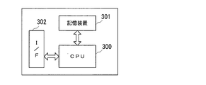
- FIG. 24 is a block diagram showing a configuration example of a computer that realizes a time calculation unit of the time measurement circuit according to the first to third embodiments of the present invention.
- FIG. 25 is a circuit diagram showing a configuration example of a conventional ring oscillator type TDC.
- FIG. 26 is a timing chart illustrating the operation of the conventional ring oscillator type TDC.
- FIG. 1 is a circuit diagram showing a configuration of a time measurement circuit according to a first embodiment of the present invention.
- the time measurement circuit uses the 1-bit binary number "1"(1'b1) as the D input, the oscillation start signal ROSC_START from the outside as the clock input, and the oscillation stop signal ROSC_STOP from the outside as the reset input, and the oscillation permission signal.
- the D flip flop circuit 10 that outputs TDC_EN, the ring oscillator 11a (oscillation circuit) that generates the high-speed clock TAP [15] (first clock) during the period when the oscillation permission signal TDC_EN is significant, and the high-speed clock TAP [15].
- the oscillator 14 that outputs the high-speed clock RCLK2 (second clock) obtained by inverting the high-speed clock TAP [15], and the buffer circuit 13.
- OR circuit 15 that outputs the result of the logical sum of the output RCLK1 and the oscillation stop signal ROSC_STOP1 as the high-speed clock ROSC_CLK1
- OR circuit 16 that outputs the result of the logical sum of the output RCLK2 of the inverter 14 and the oscillation stop signal ROSC_STOP as the high-speed clock ROSC_CLK2.
- the time measurement circuit receives a high-speed counter 12a (first counter) that counts the high-speed clock ROSC_CLK1, a high-speed counter 12b (second counter) that counts the high-speed clock ROSC_CLK2, an oscillation stop signal ROSC_STOP, and a low-speed clock MCLK.
- a high-speed counter 12a first counter
- a high-speed counter 12b second counter
- an oscillation stop signal ROSC_STOP an oscillation stop signal
- MCLK low-speed clock MCLK.
- an edge detection circuit 17 that detects the rising edge of the oscillation stop signal ROSC_STOP
- a D flip-flop circuit 18a that latches the 8-bit counting result HS_CNT1 [8: 0] of the high-speed counter 12a
- an 8-bit 8-bit counter 12b 8-bit 8-bit counter 12b.
- a DD flip-flop circuit 18b that latches the counting result HS_CNT2 [8: 0], an encoder 19 that outputs a 5-bit timing signal HS_PHASE [4: 0] indicating the phase value of the output of the ring oscillator 11a, and a D flip-flop circuit. From the rise of the oscillation start signal ROSC_START based on the selector 20 that selects one of the 8-bit outputs LATCH1 [8: 0] and LATCH2 [8: 0] of 18a and 18b and the counting result selected by the selector 20. It is provided with a time calculation unit 21 for calculating the time interval until the rise of the oscillation stop signal ROSC_STOP.
- the buffer circuit 13, the inverter 14, and the OR circuits 15 and 16 form a logic circuit 22.
- the ring oscillator 11a includes a NAND circuit 110 that takes a negative logical product of the oscillation permission signal TDC_EN and the high-speed clock TAP [15], and 15 buffer circuits 111-1 to 111-15 connected longitudinally to the output of the NAND circuit 110. And 16 D flip-flop circuits 112-1 to 112-16 in which the outputs of the NAND circuit 110 and the buffer circuits 111-1 to 111-15 are D inputs and the oscillation stop signal ROSC_STOP is the clock input. Will be done.
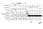
- FIG. 2 is a timing chart illustrating the operation of the time measurement circuit.
- the D flip flop circuit 10 uses the 1-bit binary number “1” (1'b1) as the D input, the oscillation start signal ROSC_START as the clock input, the oscillation stop signal ROSC_STOP as the reset input, and at the rising edge of the oscillation start signal ROSC_START.
- the oscillation permission signal TDC_EN which becomes significant and becomes unintentional (Low) at the rise of the oscillation stop signal ROSC_STOP, is output.
- the ring oscillator 11a generates a clock TAP [15] faster than the low-speed clock MCLK while the oscillation permission signal TDC_EN output from the D flip-flop circuit 10 is significant.
- the buffer circuit 13 receives the high-speed clock TAP [15] output from the ring oscillator 11a as an input, and outputs the high-speed clock RCLK1.
- the inverter 14 outputs the high-speed clock RCLK2, which is the logical inversion of the high-speed clock TAP [15] output from the ring oscillator 11a.
- the buffer circuit 13 is inserted to align the phases of the high-speed clocks RCLK1 and RCLK2.
- the OR circuit 15 outputs the result of the logical sum of the high-speed clock RCLK1 output from the buffer circuit 13 and the oscillation stop signal ROSC_STOP as the high-speed clock ROSC_CLK1.
- the OR circuit 16 outputs the result of the logical sum of the high-speed clock RCLK2 output from the inverter 14 and the oscillation stop signal ROSC_STOP as the high-speed clock ROSC_CLK2.
- the edge detection circuit 17 has an 8-bit counting result HS_CNT1 [8: 0] of the high-speed counter 12a and an 8-bit counting result HS_CNT2 [8: 0] of the high-speed counter 12b based on the oscillation stop signal ROSC_STOP and the low-speed clock MCLK.
- the capture permission signal HS_CNT_LAT indicating the timing of latching
- the high-speed counter reset signal HS_CNT_CLR for resetting the high-speed counters 12a and 12b
- the capture permission indicating that valid data is stored in the D flip-flop circuits 18a and 18b.
- Generates the signal HS_CNT_EN Generates the signal HS_CNT_EN.
- FIG. 3 is a circuit diagram showing the configuration of the edge detection circuit 17.
- the edge detection circuit 17 includes a D flip-flop circuit 170, an inverter 171, a D flip-flop circuit 172, a D flip-flop circuit 173, a D flip-flop circuit 174, an XOR circuit 175, and a D flip-flop circuit 176. It is composed of a D flip-flop circuit 178.
- the D flip-flop circuit 170 uses the oscillation stop signal ROSC_STOP as a clock input.
- the inverter 171 uses the signal obtained by inverting the output signal STOP_DET of the D flip-flop circuit 170 as the D input of the D flip-flop circuit 170.
- the D flip-flop circuit 172 uses the output signal STOP_DET of the D flip-flop circuit 170 as the D input and the low-speed clock MCLK as the clock input.
- the D flip-flop circuit 173 uses the output signal of the D flip-flop circuit 172 as the D input and the low-speed clock MCLK as the clock input.
- the D flip-flop circuit 174 uses the output signal of the D flip-flop circuit 173 as the D input and the low-speed clock MCLK as the clock input.
- the XOR circuit 175 takes in the result of the exclusive OR of the output signal of the D flip-flop circuit 173 and the output signal of the D flip-flop circuit 174 and outputs it as the permission signal HS_CNT_LAT.
- the D flip-flop circuit 176 outputs the capture permission signal HS_CNT_EN with the capture permission signal HS_CNT_LAT as the D input and the low-speed clock MCLK as the clock input.
- the D flip-flop circuit 178 outputs a high-speed counter reset signal HS_CNT_CLR with the capture permission signal HS_CNT_LAT as the D input and the result of inverting the low-speed clock MCLK as the clock input.
- the high-speed counter 12a counts the rise of the high-speed clock ROSC_CLK1 while the high-speed counter reset signal HS_CNT_CLR is involuntary (High), and outputs an 8-bit counting result HS_CNT1 [8: 0].
- the high-speed counter 12b counts the rise of the high-speed clock ROSC_CLK2 while the high-speed counter reset signal HS_CNT_CLR is involuntary (High), and outputs an 8-bit counting result HS_CNT2 [8: 0].
- the counting results HS_CNT1 [8: 0] and HS_CNT2 [8: 0] of these high-speed counters 12a and 12b are initialized to 0 when the high-speed counter reset signal HS_CNT_CLR falls.
- the D flip-flop circuit 18a latches the 8-bit counting result HS_CNT1 [8: 0] of the high-speed counter 12a at the rise of the capture permission signal HS_CNT_LAT, and holds it until the next capture permission signal HS_CNT_LAT rises.
- the D flip-flop circuit 18b latches the 8-bit counting result HS_CNT2 [8: 0] of the high-speed counter 12b at the rising edge of the capture permission signal HS_CNT_LAT, and holds the capture permission signal HS_CNT_LAT until the next rise.
- the encoder 19 is based on the 16-bit signal ROSC_PHASE [15: 0] output from the D flip-flop circuits 112-1 to 112-16, and the 5-bit timing signal HS_PHASE [15: 0] indicating the phase value of the output of the ring oscillator 11a. 4: 0] is output.
- the timing signal HS_PHASE [4: 0] is a signal obtained by encoding the 16-bit signal ROSC_PHASE [15: 0] into 5 bits.
- the selector 20 is an 8-bit counting result LATCH1 [8: 0], LATCH2 [8: 0] latched by the D flip-flop circuits 18a and 18b based on the 5-bit timing signal HS_PHASE [4: 0] output from the encoder 19. 8: 0], the counting result obtained by the high-speed counter on which the glitch (counting error) does not occur is selected as the true value.
- the time calculation unit 21 captures the counting result output from the selector 20 when the capture permission signal HS_CNT_EN becomes significant (High).
- the time calculation unit 21 calculates the time interval from the rise of the oscillation start signal ROSC_START to the rise of the oscillation stop signal ROSC_STOP based on the captured counting result.
- the TAP [15] which is the output of the ring oscillator 11a until the ring oscillator 11a receives the oscillation stop signal ROSC_STOP indicating the measurement stop.
- the timing of the oscillation stop signal ROSC_STOP may malfunction.
- the output TAP [15] of the ring oscillator 11a and its inverted signal are counted by different high-speed counters 12a and 12b, respectively, and the obtained counting result is the counting result of the one in which glitch is not generated.
- the high-speed clock RCLK1 in which the high-speed clock TAP [15] output from the ring oscillator 11a is passed through the buffer circuit 13 and the high-speed clock RCLK2 in which the high-speed clock TAP [15] is logically inverted by the inverter 14 are combined.
- the OR circuits 15 and 16 are OR-masked by the oscillation stop signals ROSC_STOP, and the OR-masked high-speed clocks ROSC_CLK1 and ROSC_CLK2 are counted by separate high-speed counters 12a and 12b, respectively.
- the above-mentioned glitch may occur, but the phase relationship between the rising edge of the oscillation start signal ROSC_START and the high-speed clocks RCLK1 and RCLK2 can be found from the timing signal HS_PHASE [4: 0]. Since it can be determined, the counting result obtained by the high-speed counter on which glitch does not occur may be selected as the true value.
- FIG. 4 shows the relationship between the high-speed clocks RCLK1 and RCLK2 and the timing signal HS_PHASE [4: 0].
- the boundary between the minimum Low width (Min Error) that the high-speed counters 12a and 12b cannot accept and the selection of LATCH1 [8: 0] and LATCH2 [8: 0] determined based on this Min Error is defined.
- ⁇ t in FIG. 4 indicates the delay time per stage of the delay circuit (NAND circuit 110 and buffer circuits 111-1 to 111-15) of the ring oscillator 11a.
- the selector 20 has a glitch (counting error) among the 8-bit counting results LATCH1 [8: 0] and LATCH2 [8: 0] latched by the D flip-flop circuits 18a and 18b.
- the counting result obtained by the non-fast counter is selected as the true value. Such selection can be made based on the value of the 5-bit timing signal HS_PHASE [4: 0].
- the selector 20 has a predetermined first phase value (in this embodiment) in which the phase of the high-speed clock RCLK1 is smaller than 180 ° from 0 ° (the value of the timing signal HS_PHASE [4: 0] is 0).
- the counting result LATCH1 [8: 0] is selected in the range of 101.25 ° and the value of the timing signal HS_PHASE [4: 0] is less than 9).
- the selector 20 has a predetermined second phase value (281.25 ° in this embodiment, timing signal HS_PHASE [4:) in which the phase of the high-speed clock RCLK1 is 180 ° or more and smaller than 360 ° from the first phase value.
- the counting result LATCH2 [8: 0] is selected, and when the phase of the high-speed clock RCLK1 is greater than or equal to the second phase value and less than 360 °, the counting result LATCH1 [8: 0] is selected. select.
- the selector 20 selects either the 8-bit counting result LATCH1 [8: 0] or LATCH2 [8: 0], the elapsed time from the falling edge of the high-speed clocks RCLK1 and RCLK2 is the lowest Low.
- the counting result of the high-speed counter that counts the high-speed clock that exceeds the time obtained by adding the predetermined margin width to the width (MinError) is selected as the true value.
- the selector 20 selects the counting result LATCH1 [8: 0], and the elapsed time from the fall of the high-speed clock RCLK1 is not sufficient for the minimum Low width, and the elapsed time from the fall of the high-speed clock RCLK2 is not sufficient.
- the counting result LATCH2 [8: 0] is selected in a period in which the elapsed time has a sufficient margin for the minimum Low width.
- the boundary is determined on the assumption that the minimum Low width holding period (Min Error) of the clocks of the flip-flops constituting the high-speed counters 12a and 12b is 250 ps and the resolution of the TDC is 50 ps.
- the high-speed clocks ROSC_CLK1 and ROSC_CLK2 whose high-speed clocks RCLK1 and RCLK2 are OR-masked by the oscillation stop signal ROSC_STOP are set to the high-speed counter 12a, It can be avoided by using it as a clock of 12b.
- the time calculation unit 21 starts oscillation after subtracting 1 from the value of the counting result LATCH1 [8: 0] or LATCH2 [8: 0] depending on the phase relationship between the high-speed clocks ROSC_CLK1 and ROSC_CLK2 and the oscillation stop signal ROSC_STOP. It is necessary to calculate the time interval from the rise of the signal ROSC_START to the rise of the oscillation stop signal ROSC_STOP.
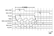
- FIG. 5 shows a case where the rise of the oscillation stop signal ROSC_STOP is received at the timing when the value of the timing signal HS_PHASE [4: 0] is 0 (the phase of the high-speed clock RCLK1 is 0 °).
- glitches are generated in the high-speed clock ROSC_CLK2.
- the selector 20 selects the counting result LATCH1 [8: 0] (HS_CNT1 [8: 0]) by the above operation. If the value of the timing signal HS_PHASE [4: 0] is 0 when the capture permission signal HS_CNT_EN becomes significant (High), the time calculation unit 21 subtracts 1 from the captured count result LATCH1 [8: 0]. No need.
- FIG. 6 shows a case where the rise of the oscillation stop signal ROSC_STOP is received at the timing when the value of the timing signal HS_PHASE [4: 0] is 9 (the phase of the high-speed clock RCLK1 is 101.25 °).
- the selector 20 selects the counting result LATCH2 [8: 0] (HS_CNT2 [8: 0]) by the above operation. If the value of the timing signal HS_PHASE [4: 0] is 9 when the capture permission signal HS_CNT_EN becomes significant (High), the time calculation unit 21 subtracts 1 from the captured count result LATCH2 [8: 0]. Then calculate the time interval.
- FIG. 7 shows a case where the rise of the oscillation stop signal ROSC_STOP is received at the timing when the value of the timing signal HS_PHASE [4: 0] is 16 (the phase of the high-speed clock RCLK1 is 180 °).
- glitches are generated in the high-speed clock ROSC_CLK1.
- the selector 20 selects the counting result LATCH2 [8: 0] (HS_CNT2 [8: 0]) by the above operation.
- the time calculation unit 21 subtracts 1 from the captured count result LATCH2 [8: 0]. Then calculate the time interval.
- FIG. 8 shows a case where the rise of the oscillation stop signal ROSC_STOP is received at the timing when the value of the timing signal HS_PHASE [4: 0] is 25 (the phase of the high-speed clock RCLK1 is 281.25 °).
- the selector 20 selects the counting result LATCH1 [8: 0] (HS_CNT1 [8: 0]) by the above operation.
- the time calculation unit 21 subtracts 1 from the captured count result LATCH1 [8: 0]. Then calculate the time interval.
- Fig. 9 shows the necessity of correcting the above counting results.
- the number of stages of the delay circuit (NAND circuit 110 and buffer circuits 111-1 to 111-15) of the ring oscillator 11a is 16 stages (TAP [0] to TAP [15]). Is not a problem for the present invention other than 16. However, if the number of stages is a power of 2, the count values of the high-speed counters 12a and 12b (LATCH1 [8: 0], LATCH2 [8: 0]) and the phase value of the ring oscillator 11a (HS_PHASE [4: 0]). Can be simplified.
- the time measurement value is such that HS_PHASE is connected to the lower bit side and LATCH1 is connected to the upper bit side, such as ⁇ LATCH1 [8: 0], HS_PHASE [4: 0] ⁇ . It can be obtained by.
- a simplification of the combination of the count value and the phase value when the number of stages of the ring oscillator 11a is not a power of 2 is described in, for example, Japanese Patent No. 2868266.
- FIG. 10 is a circuit diagram showing the configuration of the time measurement circuit according to this embodiment, and the same configuration as that of FIG. 1 is designated by the same reference numeral.
- the time measurement circuit of this embodiment includes a D flip-flop circuit 10, a ring oscillator 11a (oscillation circuit), high-speed counters 12a and 12b (first and second counters), an edge detection circuit 17, and a D flip-flop.
- the result of the logic sum of the high-speed clock ROSC_CLK1 (TAP [15]) output from the circuits 18a and 18b, the encoder 19, the selector 20a, the time calculation unit 21, and the ring oscillator 11a and the oscillation stop signal ROSC_STOP is obtained as the high-speed clock ROSC_CLK2.
- It is composed of an OR circuit 23 (logic circuit) that outputs as.
- the configuration and operation of the D flip-flop circuit 10 and the ring oscillator 11a are as described in the first embodiment.
- the high-speed counter 12a of this embodiment counts the rise of the high-speed clock ROSC_CLK1 (TAP [15]) output from the ring oscillator 11a while the high-speed counter reset signal HS_CNT_CLR is involuntary (High), and has 8 bits.
- the counting result HS_CNT1 [8: 0] is output.
- the OR circuit 23 outputs the result of the logical sum of the high-speed clock ROSC_CLK1 (TAP [15]) and the oscillation stop signal ROSC_STOP as the high-speed clock ROSC_CLK2.
- the high-speed counter 12b counts the rise of the high-speed clock ROSC_CLK2 while the high-speed counter reset signal HS_CNT_CLR is involuntary (High), and outputs an 8-bit counting result HS_CNT2 [8: 0].
- the selector 20a causes a glitch (counting error) among the 8-bit counting results LATCH1 [8: 0] and LATCH2 [8: 0] latched by the D flip-flop circuits 18a and 18b.
- the counting result obtained by the higher-speed counter is selected as the true value, but since the buffer circuit 13 and the inverter 14 are not used, the phase of the high-speed clock ROSC_CLK1 (TAP [15]), which is the boundary for switching the selection, is selected.
- the timing signal HS_PHASE [4: 0] value) is different from that of the first embodiment.
- FIG. 11 shows the relationship between ROSC_CLK1 (TAP [15]) and the timing signal HS_PHASE [4: 0].
- the selector 20a has a phase of the high-speed clock ROSC_CLK1 (TAP [15]) input to the high-speed counter 12a from 0 ° (the value of the timing signal HS_PHASE [4: 0] is 0) to 180 °.
- the counting result LATCH2 [8: 0] is selected in the range of less than a small predetermined first phase value (123.75 ° in this embodiment, the value of the timing signal HS_PHASE [4: 0] is 11).
- the selector 20a has a predetermined second phase value (303.75 ° in this embodiment) in which the phase of the high-speed clock ROSC_CLK1 (TAP [15]) is 180 ° or more and smaller than 360 ° from the first phase value.
- the counting result LATCH1 [8: 0] is selected, and the phase of the high-speed clock ROSC_CLK1 (TAP [15]) is greater than or equal to the second phase value and less than 360 °. In the range of, the counting result LATCH2 [8: 0] is selected.
- the boundary is determined on the assumption that the minimum Low width holding period (Min Error) of the clocks of the flip-flops constituting the high-speed counters 12a and 12b is 250 ps and the resolution of the TDC is 50 ps. ing.
- the time calculation unit 21 captures the counting result output from the selector 20a at the rise of the capture permission signal HS_CNT_LAT, and the time interval from the rise of the oscillation start signal ROSC_START to the rise of the oscillation stop signal ROSC_STOP. Is calculated. In this way, in this embodiment, the same effect as in the first embodiment can be obtained.
- the time calculation unit 21 subtracts 1 from the value of the counting result LATCH1 [8: 0] or LATCH2 [8: 0] depending on the phase relationship between the high-speed clock ROSC_CLK2 and the oscillation stop signal ROSC_STOP. Therefore, it is necessary to calculate the time interval from the rise of the oscillation start signal ROSC_START to the rise of the oscillation stop signal ROSC_STOP.
- the phase (value of the timing signal HS_PHASE [4: 0]) of the high-speed clock ROSC_CLK1 (TAP [15]), which is the boundary for switching the selection of the selector 20a, is the first. Since it is different from the first embodiment, the determination as to whether or not to correct the counting result is also different from the first embodiment.
- the case where the rise of the oscillation stop signal ROSC_STOP is received at the timing when the value of the timing signal HS_PHASE [4: 0] is 0 (the phase of ROSC_CLK1 (TAP [15]) is 0 °) is shown. ..
- glitches occur in the high-speed clock ROSC_CLK1.
- the selector 20 selects the counting result LATCH2 [8: 0] (HS_CNT2 [8: 0]) by the above operation.
- the time calculation unit 21 subtracts 1 from the captured count result LATCH2 [8: 0]. No need.
- FIG. 13 shows the case where the rise of the oscillation stop signal ROSC_STOP is received at the timing when the value of the timing signal HS_PHASE [4: 0] is 11 (the phase of the high-speed clock ROSC_CLK1 (TAP [15]) is 123.75 °). It shows.
- the selector 20 selects the counting result LATCH1 [8: 0] (HS_CNT1 [8: 0]) by the above operation.
- the time calculation unit 21 subtracts 1 from the captured count result LATCH1 [8: 0]. Then calculate the time interval.
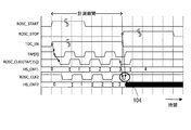
- FIG. 14 shows a case where the rise of the oscillation stop signal ROSC_STOP is received at the timing when the value of the timing signal HS_PHASE [4: 0] is 16 (the phase of the high-speed clock ROSC_CLK1 (TAP [15]) is 180 °). There is. In 104 of FIG. 14, glitches occur in the high-speed clock ROSC_CLK2.
- the selector 20 selects the counting result LATCH1 [8: 0] (HS_CNT1 [8: 0]) by the above operation.
- the time calculation unit 21 subtracts 1 from the captured count result LATCH1 [8: 0]. Then calculate the time interval.
- the rise of the oscillation stop signal ROSC_STOP is received at the timing when the value of the timing signal HS_PHASE [4: 0] is 27 (the phase of the high-speed clock ROSC_CLK1 (TAP [15]) is 303.75 °). It shows.
- the selector 20 selects the counting result LATCH2 [8: 0] (HS_CNT2 [8: 0]) by the above operation.
- the time calculation unit 21 subtracts 1 from the captured count result LATCH2 [8: 0]. Then calculate the time interval.
- FIG. 11 shows the necessity of correcting the above counting results, as shown in FIG. Similar to the first embodiment, the time calculation unit 21 takes in the counting result selected by the selector 20 when the phase of the high-speed clock RCLK1 is in the range of the first phase value or more and less than 360 °. The time interval may be calculated after subtracting 1 from the counting result.
- FIG. 17 is a circuit diagram showing the configuration of the time measurement circuit according to the present embodiment, and the same configurations as those in FIGS. 1 and 10 are designated by the same reference numerals.
- the time measurement circuit of this embodiment includes a D flip flop circuit 10, a ring oscillator 11a (oscillation circuit), high-speed counters 12a and 12b (first and second counters), a buffer circuit 13, an inverter 14, and the like.
- the signal ROSC_STOP (first stop signal) is selected and output, and the start signal DBG_START (second start signal) and stop signal DBG_STOP (second stop signal) output from the test execution unit described later at the time of test execution are output. It is provided with an operation setting circuit 24 that selects and outputs a stop signal ROSC_STOPb (third stop signal) at the end of the test.
- the time measurement circuit of the present embodiment masks the high-speed clock RCLK1 later than the high-speed clock RCLK2 and unmasks the high-speed clock RCLK2 later than the high-speed clock RCLK2, and the high-speed clock RCLK2.
- the mask release timing control circuit 25 that generates a stop signal for masking before RCLK1 and releasing the mask before the high-speed clock RCLK1 from the stop signal ROSC_STOPa output from the operation setting circuit 24, and the high-speed clock RCLK1.
- the OR circuit 26 that outputs the result of the logical sum of the stop signals output from the mask release timing control circuit 25 as the high-speed clock ROSC_CLK1, and the result of the logical sum of the stop signals output from the high-speed clock RCLK2 and the mask release timing control circuit 25. Is provided with an OR circuit 27 that outputs the high-speed clock ROSC_CLK2.
- the buffer circuit 13, the inverter 14, the mask release timing control circuit 25, and the OR circuits 26 and 27 form a logic circuit 28.
- an operation setting circuit 24 capable of activating the ring oscillator 11a by the START and STOP signals (DBG_START, DBG_STOP) from the time measurement circuit 21a and a high-speed clock are used with respect to the first embodiment.
- the mask release timing control circuit 25 for controlling the mask release timing of RCLK1 and RCLK2 and the OR circuits 26 and 27 are added.
- FIG. 18 is a circuit diagram showing the configuration of the operation setting circuit 24.
- FIG. 19 is a circuit diagram showing the configuration of the mask release timing control circuit 25.
- the operation setting circuit 24 includes a selector 240, a selector 241 and an AND circuit 242.
- the selector 240 selects either the oscillation stop signal ROSC_STOP or the stop signal DBG_STOP output from the time calculation unit 21a according to the selection instruction signal ROSC_SEL output from the time calculation unit 21a, and outputs the stop signal ROSC_STOPa.
- the selector 241 selects either the oscillation start signal ROSC_START or the start signal DBG_START output from the time calculation unit 21a according to the selection instruction signal ROSC_SEL, and outputs the start signal ROSC_STARTa.
- the AND circuit 242 outputs the result of the logical product of the stop signal ROSC_STOPa output from the selector 240 and the negation of the test instruction signal ROSC_TEST output from the time calculation unit 21a as the stop signal ROSC_STOPb.
- the D flip-flop circuit 10 of this embodiment uses the start signal ROSC_STARTa output from the operation setting circuit 24 as a clock input instead of the oscillation start signal ROSC_START, and is output from the operation setting circuit 24 instead of the oscillation stop signal ROSC_STOP.
- the stop signal ROSC_STOPb is used as the reset input.
- the D flip-flop circuits 112-1 to 112-16 of the ring oscillator 11a of this embodiment use the stop signal ROSC_STOPb as the clock input instead of the oscillation stop signal ROSC_STOP.
- the edge detection circuit 17a of this embodiment receives the stop signal ROSC_STOPa instead of the oscillation stop signal ROSC_STOP, and based on the stop signal ROSC_STOPa, the low-speed clock MCLK, and the test instruction signal ROSC_TEST, immediately after the rise of the stop signal ROSC_STOPa.
- the capture permission signal HS_CNT_LAT that becomes significant at the fall of the low-speed clock MCLK, the high-speed counter reset signal HS_CNT_CLR that becomes significant at the fall of the capture permission signal HS_CNT_LAT, and the oscillation stop signal ROSC_STOPa are used for the low-speed clock MCLK.
- a capture permission signal HS_CNT_EN delayed by 1/2 clock is generated.
- FIG. 20 is a block diagram showing the configuration of the time calculation unit 21a of this embodiment.
- the time calculation unit 200 realizes the same function as the time calculation unit 21 of the first and second embodiments.
- the test execution unit 201 tests the delay circuit (NAND circuit 110 and buffer circuits 111-1 to 111-15) of the ring oscillator 11a.
- FIG. 21 is a timing chart for explaining the operation of the time measurement circuit of this embodiment during the test.
- the test execution unit 201 sends the test instruction signal ROSC_TEST as shown in FIG. 21, for example, by an instruction from the user.
- the significant high level is set, and the selection instruction signal ROSC_SEL is set to the high level.
- the selector 240 of the operation setting circuit 24 selects the stop signal DBG_STOP from the oscillation stop signal ROSC_STOP and the stop signal DBG_STOP output from the test execution unit 201 to select the stop signal ROSC_STOPa. Output as.
- the selector 241 of the operation setting circuit 24 selects the start signal DBG_START from the oscillation start signal ROSC_START and the start signal DBG_START output from the test execution unit 201 because the selection instruction signal ROSC_SEL is at the High level, and the start signal ROSC_STARTa Output as.
- the AND circuit 242 of the operation setting circuit 24 outputs the result of the logical product of the stop signal ROSC_STOPa output from the selector 240 and the negation of the test instruction signal ROSC_TEST output from the test execution unit 201 as the stop signal ROSC_STOPb.
- the stop signal ROSC_STOPb is low while the test instruction signal ROSC_TEST is at the High level during the test.
- the stop signal ROSC_STOPb becomes significant (High) when the stop signal DBG_STOP rises, for example, when the test instruction signal ROSC_TEST becomes Low after the test is completed according to an instruction from the user.
- the D flipflop circuit 10 sets the oscillation permission signal TDC_EN to be significant (High) at the rise of the first start signal ROSC_STARTa (DBG_START) during the test, and makes the oscillation permission signal TDC_EN unintentional (Low) at the rise of the stop signal ROSC_STOPb. Therefore, the ring oscillator 11a operates in a free run during the period when the oscillation permission signal TDC_EN is significant (High).
- the oscillation stop signal ROSC_STOP is output as the stop signal ROSC_STOPb.
- the test execution unit 201 periodically issues a stop signal DBG_STOP in synchronization with the low-speed clock MCLK, but the ring oscillator 11a does not stop even if the stop signal DBG_STOP reaches the High level.
- the test execution unit 201 acquires the 5-bit timing signal HS_PHASE [4: 0] output from the encoder 19 at the rising edge of the stop signal DBG_STOP, and based on the value of this timing signal HS_PHASE [4: 0], The 8-bit counting results LATCH1 [8: 0] and LATCH2 [8: 0] latched by the D flip-flop circuits 18a and 18b are acquired.
- the frequency of the ring oscillator 11a is not fixed and is not synchronized with the low-speed clock MCLK, the value obtained even if the test execution unit 201 periodically acquires the timing signal HS_PHASE [4: 0] is randomly obtained. Change.
- the test execution unit 201 Based on the value of the timing signal HS_PHASE [4: 0], the test execution unit 201 has the first phase value (101.25 °, the value of the timing signal HS_PHASE [4: 0]) of the high-speed clock RCLK1 is 9. ) Is the value immediately before (the value of the timing signal HS_PHASE [4: 0] is 8), and the counting results LATCH1 [8: 0] and LATCH2 [8: 0] are acquired and compared. Further, the test execution unit 201 may acquire and compare the counting results LATCH1 [8: 0] and LATCH2 [8: 0] when the phase of the high-speed clock RCLK1 is the first phase value.
- test execution unit 201 has a counting result LATCH1 [8: 0], LATCH2 when the phase of the high-speed clock RCLK1 is a value immediately after the first phase value (the value of the timing signal HS_PHASE [4: 0] is 10). [8: 0] may be acquired and compared. In FIG. 21, these timings are represented by Phase 1.
- the phase of the high-speed clock RCLK1 is the value immediately before the second phase value (281.25 °, the value of the timing signal HS_PHASE [4: 0] is 25) (timing signal HS_PHASE [4: 0]). ] Is 24), the counting results LATCH1 [8: 0] and LATCH2 [8: 0] are acquired and compared. Further, the test execution unit 201 may acquire and compare the counting results LATCH1 [8: 0] and LATCH2 [8: 0] when the phase of the high-speed clock RCLK1 is the second phase value.
- test execution unit 201 has a counting result LATCH1 [8: 0], LATCH2 when the phase of the high-speed clock RCLK1 is a value immediately after the second phase value (the value of the timing signal HS_PHASE [4: 0] is 26). [8: 0] may be acquired and compared. In FIG. 21, these timings are represented by Phase 2.
- the values of the counting results LATCH1 [8: 0] and LATCH2 [8: 0] should both be count values that do not violate the Low width on the high-speed counters 12a and 12b, so the test
- the execution unit 201 compares the counting results LATCH1 [8: 0] and LATCH2 [8: 0] acquired at the timing of Phase 1 and similarly obtains the counting results LATCH1 [8: 0] and LATCH2 [8: 0] at the timing of Phase 2. 8: 0] is compared.
- the test execution unit 201 sets the delay circuit (NAND circuit 110 and buffer circuit 111-1 to 11a) of the ring oscillator 11a. If 111-15) is determined to be normal and the counting results LATCH1 [8: 0] and LATCH2 [8: 0] do not match, it is determined that the delay circuit has failed.
- a method of outputting the determination result for example, there are a method of displaying the content notifying the determination result and transmitting the information notifying the determination result to the outside.
- the mask release timing control circuit 25 controls the mask release timing by the oscillation stop signal ROSC_STOP when performing a test as in this embodiment. There is a need.
- the mask release timing control circuit 25 includes an AND circuit 250, an AND circuit 251, a D flip-flop circuit 252, and a D flip-flop circuit 253D flip-flop circuit 254.
- the AND circuit 250 outputs the result of the logical product of the high-speed clock RCLK1 output from the buffer circuit 13 and the test instruction signal ROSC_TEST output from the time calculation unit 21a.
- the AND circuit 251 outputs the result of the logical product of the high-speed clock RCLK2 output from the inverter 14 and the test instruction signal ROSC_TEST.
- the D flip-flop circuit 252 uses the stop signal ROSC_STOPa output from the operation setting circuit 24 as the D input, and the output of the AND circuit 251 as the clock input.
- the D flip-flop circuit 253 uses the output STOP_RCLK2_D1 of the D flip-flop circuit 252 as the D input and the stop signal ROSC_STOPa as the clock input.
- the D flip-flop circuit 254 uses the output STOP_RCLK2_D2 of the D flip-flop circuit 253 as the D input and the output of the AND circuit 250 as the clock input.
- the OR circuit 26 outputs the result of the logical sum of the high-speed clock RCLK1 and the output STOP_RCLK1_D3 (fourth stop signal) of the D flip-flop circuit 254 of the mask release timing control circuit 25 and the stop signal ROSC_STOPa as the high-speed clock ROSC_CLK1.
- the OR circuit 27 outputs the result of the logical sum of the high-speed clock RCLK2, the output STOP_RCLK2_D2 (fifth stop signal) of the D flip-flop circuit 253 of the mask release timing control circuit 25, and the stop signal ROSC_STOPa as the high-speed clock ROSC_CLK2.
- FIG. 22 is a timing chart illustrating the operation of the mask release timing control circuit 25. Note that FIG. 22 shows the case where the value of the timing signal HS_PHASE [4: 0] is 24 or 25.
- the buffer circuit 13 and the inverter 14 of the first to third embodiments when the oscillation permission signal TDC_EN becomes significant (High), the high-speed clock RCLK2 rises ⁇ the high-speed clock RCLK1 rises ⁇ high speed.
- the operation of alternately starting up the high-speed clocks RCLK2 and RCLK1 is performed, such as rising of the clock RCLK2 ⁇ rising of the high-speed clock RCLK1.
- the high-speed counter 12b (HS_CNT2 [8: 0]) and the high-speed counter 12a (HS_CNT1 [8: 0]) are counted up in this order. Therefore, even when the mask is released, as shown in the timing chart of FIG. 22, the mask release timing is set in the order of rising of the high-speed clock RCLK2 ⁇ rising of the high-speed clock RCLK1 ⁇ rising of the high-speed clock RCLK2 ⁇ rising of the high-speed clock RCLK1. Control.
- STOP_RCLK2_D1 in FIG. 22 shows the output of the D flip-flop circuit 252
- STOP_RCLK2_D2 shows the output of the D flip-flop circuit 253
- STOP_RCLK1_D3 shows the output of the D flip-flop circuit 254.
- the output STOP_RCLK2_D2 of the D flip-flop circuit 253 is used in the OR circuit 27 to mask the high-speed clock RCLK2.
- the output STOP_RCLK1_D3 of the D flip-flop circuit 254 is used as a mask for the high-speed clock RCLK1 in the OR circuit 26.
- the output STOP_RCLK2_D2 of the D flip-flop circuit 253 falls earlier than the output STOP_RCLK1_D3 of the D flip-flop circuit 254, and the high-speed clock RCLK2 is unmasked earlier than the high-speed clock RCLK1.
- the count-up is restarted in the order of the high-speed counter 12b (HS_CNT2 [8: 0]) and the high-speed counter 12a (HS_CNT1 [8: 0]).
- the counting results LATCH1 [8: 0] and LATCH2 [8: 0] are compared at the timings of Phase1 and Phase2, but the value of the timing signal HS_PHASE [4: 0] is 24, 25 or In the case of 26 (when the phase of the high-speed clock RCLK1 is the value immediately before the second phase value, the value immediately after the second phase value or the second phase value), if there is no failure in the delay circuit of the ring oscillator 11a. , As shown at 107 in FIG. 22, the counting results LATCH1 [8: 0] and LATCH2 [8: 0] always match.
- the high-speed clock ROSC_CLK2 rises once more than ROSC_CLK1, so as shown at 108 in FIG. 23, with respect to the counting result LATCH1 [8: 0].
- the count value is 1 larger for LATCH2 [8: 0].
- the test execution unit 201 subtracts 1 from the counting result LATCH2 [8: 0] and then subtracts 1 from the counting result LATCH1 [8: 0]. 0] is compared with the subtracted LATCH2 [8: 0], and if the counting results LATCH1 [8: 0] and LATCH2 [8: 0] match, the delay circuit of the ring oscillator 11a is normal. If the counting result LATCH1 [8: 0] and LATCH2 [8: 0] do not match, it is determined that the delay circuit has failed.
- the normal operation is the same as in the first embodiment. As described above, since the test instruction signal ROSC_TEST becomes the High level when the test is executed, the operation of the mask release timing control circuit 25 becomes effective by the AND circuits 250 and 251 of the mask release timing control circuit 25. On the other hand, since the test instruction signal ROSC_TEST is normally at the Low level, the operation of the mask release timing control circuit 25 is invalid (the outputs of the AND circuits 250 and 251 are always at the Low level).
- the OR circuit 26 outputs the result of the logical sum of the high-speed clock RCLK1 output from the buffer circuit 13 and the stop signal ROSC_STOPa (ROSC_STOP) as the high-speed clock ROSC_CLK1 as in the OR circuit 15 of the first embodiment. .. Similar to the OR circuit 16, the OR circuit 27 outputs the result of the logical sum of the high-speed clock RCLK2 output from the inverter 14 and the stop signal ROSC_STOPa (ROSC_STOP) as the high-speed clock ROSC_CLK2.
- the self-test function of this embodiment it is not necessary to select a tester capable of controlling the oscillation start signal ROSC_START and the oscillation stop signal ROSC_STOP with a resolution of several tens of ps as the IC shipping inspection tester, and the oscillator oscillates from the outside. Since the test can be performed without inputting the start signal ROSC_START and the oscillation stop signal ROSC_STOP, the test time of the IC equipped with the time measurement circuit can be shortened. As a result, in this embodiment, it is possible to contribute to the cost reduction of the IC.
- the time calculation units 21 and 21a of the time measurement circuit described in the first to third embodiments are provided by a computer provided with a CPU (Central Processing Unit), a storage device and an interface, and a program for controlling these hardware resources. It can be realized.
- a configuration example of this computer is shown in FIG.
- the computer includes a CPU 300, a storage device 301, and an interface device (hereinafter, abbreviated as I / F) 302.
- the selector 20, the edge detection circuits 17, 17a, the D flip-flop circuits 18a, 18b, the encoder 19, the operation setting circuit 24, and the mask release timing control circuit 25 are connected to the I / F 302.
- a program for realizing the present invention is stored in the storage device 301.
- the CPU 300 executes the processes described in the first to third embodiments according to the program stored in the storage device 301.
- the present invention can be applied to a technique for measuring time on the order of psec.
Landscapes
- Engineering & Computer Science (AREA)
- Power Engineering (AREA)
- Physics & Mathematics (AREA)
- General Physics & Mathematics (AREA)
- Manipulation Of Pulses (AREA)
- Measurement Of Unknown Time Intervals (AREA)
- Stabilization Of Oscillater, Synchronisation, Frequency Synthesizers (AREA)
Abstract
低消費電力動作と正確な時間計測を実現するために、時間計測回路は、高速クロック(RCLK1)と、高速クロックRCLK1を反転させた高速クロックRCLK2をそれぞれ停止信号ROSC_STOPでマスクする論理回路(22)と、停止信号ROSC_STOPでマスクされた高速クロックROSC_CLK1,ROSC_CLK2を数える高速カウンタ(12a,12b)と、高速カウンタ(12a,12b)の計数結果のうち、受付不可能な時間幅のクロック入力が発生していない方のカウンタによって得られた計数結果を選択するセレクタ(20)と、セレクタ(20)によって選択された計数結果を基に開始信号ROSC_STARTの入力から停止信号ROSC_STOPの入力までの時間間隔を算出する時間算出部(21)とを備える。
Description
本発明は、高精度な時間測定を行うことが可能な時間計測回路に関する。
psecオーダーの高分解能な時間測定を行う場合、論理回路のゲート遅延を用いるTDC(Time-to-Digital Converter)と呼ばれる手法(非特許文献1参照)が広く知られている。このTDCは、DLL(Delay Locked Loop)、またはPLL(Phase Locked Loop)をベースとした構成とするのが一般的である。しかし、DLLやPLLはクロックの発振の安定化に時間を要するので、時間計測開始前にTDCを動作させておく必要があり、低消費電力化の実現が難しいという問題点があった。
例えばガスメータ向け超音波流量計は、超音波の伝搬時間差を低消費電力かつ高精度、高分解能で測定する必要があるため、高速カウンタの動作期間(高速クロックの発振期間)をできる限り短くする必要がある。しかし、上記のとおりDLL方式のTDCとPLL方式のTDCは遅延回路の発振安定化に時間を要するため、高速クロックの発振期間が長くなり消費電力面で不利である。
TDCの動作時間(高速クロックの発振時間)を最小にして、低消費電力動作を目指す場合、例えば特許文献1に開示されたリングオシレータ型の構成が考えられる。
図25は、従来のリングオシレータ型TDCの構成を示す回路図である。リングオシレータ型TDCは、Dフリップフロップ回路10と、リングオシレータ11と、高速カウンタ12とから構成される。Dフリップフロップ回路10は、1ビットの2進数“1”(1’b1)をD入力とし、発振開始信号ROSC_STARTをクロック入力とし、発振停止信号ROSC_STOPをリセット入力とし、発振許可信号TDC_ENを出力する。リングオシレータ11は、発振許可信号TDC_ENが有意の期間中に高速クロックTAP[2]を生成する。高速カウンタ12は、高速クロックをカウントする。
図25は、従来のリングオシレータ型TDCの構成を示す回路図である。リングオシレータ型TDCは、Dフリップフロップ回路10と、リングオシレータ11と、高速カウンタ12とから構成される。Dフリップフロップ回路10は、1ビットの2進数“1”(1’b1)をD入力とし、発振開始信号ROSC_STARTをクロック入力とし、発振停止信号ROSC_STOPをリセット入力とし、発振許可信号TDC_ENを出力する。リングオシレータ11は、発振許可信号TDC_ENが有意の期間中に高速クロックTAP[2]を生成する。高速カウンタ12は、高速クロックをカウントする。
図26は、図25のリングオシレータ型TDCの動作を説明するタイミングチャートである。Dフリップフロップ回路10は、1ビットの2進数“1”(1’b1)をD入力とし、発振開始信号ROSC_STARTをクロック入力とし、発振停止信号ROSC_STOPをリセット入力とし、図26に示すように発振開始信号ROSC_STARTの立ち上がりで有意(High)となり、発振停止信号ROSC_STOPの立ち上がりで無意(Low)となる発振許可信号TDC_ENを出力する。
リングオシレータ11は、発振許可信号TDC_ENと高速クロックTAP[2]との否定論理積をとるNAND回路110と、NAND回路110の出力TAP[0]を入力とするバッファ回路111-1と、バッファ回路111-1の出力TAP[1]を入力とし、その出力TAP[2]を高速クロックとして出力するバッファ回路111-2とから構成される。リングオシレータ11は、Dフリップフロップ回路10から出力された発振許可信号TDC_ENが有意の期間中に、図26に示すように、低速クロック(ROSC_STOP)よりも高速なクロックTAP[2]を生成する。
高速カウンタ12は、高速クロックTAP[2]の立ち上がりをカウントして計数結果HS_CNTを出力する。
高速カウンタ12は、高速クロックTAP[2]の立ち上がりをカウントして計数結果HS_CNTを出力する。
ただし、図25に示したリングオシレータ型TDCでは、発振停止信号ROSC_STOPのタイミング次第で、図26の100で示すように、高速カウンタ12を構成するフリップフロップが受け付け不可能なLow幅のクロックをリングオシレータ11が出力してしまい、高速カウンタ12の計数結果HS_CNTの値が不定となり、正しい時間を計測できないという課題があった。以下、本発明では、この意図しないタイミングで発生する微小な幅のパルスをグリッチと呼ぶ。
例えば、リングオシレータ11の出力である高速クロックTAP[2]の周波数を600MHzとすると、高速カウンタ12のカウント値がグリッチにより“1”大きくなるということは、時間計測値が期待値よりも1.67nsec大きな値となることを示す。特許文献1に開示されたような超音波流量計は、微小流量計測のためにサブナノオーダーの精度での時間計測が求められるため、流量計測値が期待値と比較して±1.67ns異なるという仕様では製品スペックを満たすことができない。
Stephan Henzler,"Time-to-Digital Converters",Springer,2010
本発明は、上記課題を解決するためになされたもので、低消費電力動作と正確な時間計測とを実現することができる時間計測回路を提供することを目的とする。
本発明の時間計測回路(第1の実施例)は、外部からの開始信号の入力のタイミングで有意となり、外部からの停止信号の入力のタイミングで無意となる発振許可信号を出力するように構成されたフリップフロップ回路と、前記発振許可信号が有意の期間中に第1のクロックを生成するように構成された発振回路と、前記第1のクロックと、前記第1のクロックを反転させた第2のクロックとをそれぞれ前記停止信号でマスクするように構成された論理回路と、前記停止信号でマスクされた第1のクロックを数えるように構成された第1のカウンタと、前記停止信号でマスクされた第2のクロックを数えるように構成された第2のカウンタと、前記第1、第2のカウンタの計数結果のうち、受付不可能な時間幅のクロック入力が発生していない方のカウンタによって得られた計数結果を選択するように構成されたセレクタと、前記停止信号の入力後に前記セレクタによって選択された計数結果を基に前記開始信号の入力から前記停止信号の入力までの時間間隔を算出するように構成された時間算出部とを備えることを特徴とするものである。
また、本発明の時間計測回路の1構成例において、前記セレクタは、前記第1のクロックの位相が0°から180°よりも小さい所定の第1の位相値未満の範囲では前記第1のカウンタの計数結果を選択し、前記第1のクロックの位相が前記第1の位相値から180°以上で360°よりも小さい所定の第2の位相値未満の範囲では前記第2のカウンタの計数結果を選択し、前記第1のクロックの位相が前記第2の位相値以上360°未満の範囲では前記第1のカウンタの計数結果を選択することを特徴とするものである。
また、本発明の時間計測回路の1構成例において、前記論理回路は、前記発振回路から出力された第1のクロックを入力とするバッファ回路と、前記発振回路から出力された第1のクロックを反転させた前記第2のクロックを生成するように構成されたインバータと、前記バッファ回路から出力された第1のクロックを前記停止信号でORマスクするように構成された第1のOR回路と、前記インバータから出力された第2のクロックを前記停止信号でORマスクするように構成された第2のOR回路とから構成されることを特徴とするものである。
また、本発明の時間計測回路の1構成例において、前記論理回路は、前記発振回路から出力された第1のクロックを入力とするバッファ回路と、前記発振回路から出力された第1のクロックを反転させた前記第2のクロックを生成するように構成されたインバータと、前記バッファ回路から出力された第1のクロックを前記停止信号でORマスクするように構成された第1のOR回路と、前記インバータから出力された第2のクロックを前記停止信号でORマスクするように構成された第2のOR回路とから構成されることを特徴とするものである。
また、本発明の時間計測回路(第2の実施例)は、外部からの開始信号の入力のタイミングで有意となり、外部からの停止信号の入力のタイミングで無意となる発振許可信号を出力するように構成されたフリップフロップ回路と、前記発振許可信号が有意の期間中に第1のクロックを生成するように構成された発振回路と、前記第1のクロックを前記停止信号でマスクした第2のクロックを生成するように構成された論理回路と、前記第1のクロックを数えるように構成された第1のカウンタと、前記第2のクロックを数えるように構成された第2のカウンタと、前記第1、第2のカウンタの計数結果のうち、受付不可能な時間幅のクロック入力が発生していない方のカウンタによって得られた計数結果を選択するように構成されたセレクタと、前記停止信号の入力後に前記セレクタによって選択された計数結果を基に前記開始信号の入力から前記停止信号の入力までの時間間隔を算出するように構成された時間算出部とを備えることを特徴とするものである。
また、本発明の時間計測回路の1構成例において、前記セレクタは、前記第1のクロックの位相が0°から180°よりも小さい所定の第1の位相値未満の範囲では前記第2のカウンタの計数結果を選択し、前記第1のクロックの位相が前記第1の位相値から180°以上で360°よりも小さい所定の第2の位相値未満の範囲では前記第1のカウンタの計数結果を選択し、前記第1のクロックの位相が前記第2の位相値以上360°未満の範囲では前記第2のカウンタの計数結果を選択することを特徴とするものである。
また、本発明の時間計測回路の1構成例において、前記論理回路は、前記発振回路から出力された第1のクロックを前記停止信号でORマスクした前記第2のクロックを生成するように構成されたOR回路から構成されることを特徴とするものである。
また、本発明の時間計測回路の1構成例において、前記論理回路は、前記発振回路から出力された第1のクロックを前記停止信号でORマスクした前記第2のクロックを生成するように構成されたOR回路から構成されることを特徴とするものである。
また、本発明の時間計測回路(第3の実施例)は、時間計測回路のテストを行うように構成されたテスト実行部と、通常時に外部から入力された第1の開始信号、第1の停止信号を選択して出力し、テスト実行時に前記テスト実行部から出力された第2の開始信号、第2の停止信号を選択して出力すると共に、テスト終了時に第3の停止信号を出力するように構成された動作設定回路と、前記第1の開始信号または前記第2の開始信号の入力のタイミングで有意となり、前記第1の停止信号または前記第3の停止信号の入力のタイミングで無意となる発振許可信号を出力するように構成されたフリップフロップ回路と、前記発振許可信号が有意の期間中に第1のクロックを生成するように構成された発振回路と、前記第1のクロックと、前記第1のクロックを反転させた第2のクロックとをそれぞれ前記第1の停止信号または前記第2の停止信号でマスクするように構成された論理回路と、前記第1の停止信号または前記第2の停止信号でマスクされた第1のクロックを数えるように構成された第1のカウンタと、前記第1の停止信号または前記第2の停止信号でマスクされた第2のクロックを数えるように構成された第2のカウンタと、前記第1、第2のカウンタの計数結果のうち、受付不可能な時間幅のクロック入力が発生していない方のカウンタによって得られた計数結果を選択するように構成されたセレクタと、通常時に前記第1の停止信号の入力後に前記セレクタによって選択された計数結果を基に前記第1の開始信号の入力から前記第1の停止信号の入力までの時間間隔を算出するように構成された時間算出部とを備え、前記テスト実行部は、テスト実行時に前記第1、第2のカウンタの計数結果を比較することにより、前記発振回路のテストを行うことを特徴とするものである。
また、本発明の時間計測回路の1構成例において、前記セレクタは、前記第1のクロックの位相が0°から180°よりも小さい所定の第1の位相値未満の範囲では前記第1のカウンタの計数結果を選択し、前記第1のクロックの位相が前記第1の位相値から180°以上で360°よりも小さい所定の第2の位相値未満の範囲では前記第2のカウンタの計数結果を選択し、前記第1のクロックの位相が前記第2の位相値以上360°未満の範囲では前記第1のカウンタの計数結果を選択することを特徴とするものである。
また、本発明の時間計測回路の1構成例において、前記テスト実行部は、前記第1のクロックの位相が前記第1の位相値の直前の値のとき、前記第1の位相値のとき、または前記第1の位相値の直後の値のときの前記第1のカウンタの計数結果と前記第2のカウンタの計数結果とを取得して比較し、さらに前記第1のクロックの位相が前記第2の位相値の直前の値のとき、前記第2の位相値のとき、または前記第2の位相値の直後の値のときの前記第1のカウンタの計数結果と前記第2のカウンタの計数結果とを取得して比較することを特徴とするものである。
また、本発明の時間計測回路の1構成例において、前記テスト実行部は、取得した前記第1のカウンタの計数結果と前記第2のカウンタの計数結果とが一致している場合に、前記発振回路が正常と判定し、前記第1のカウンタの計数結果と前記第2のカウンタの計数結果とが不一致の場合に、前記発振回路が故障していると判定することを特徴とするものである。
また、本発明の時間計測回路の1構成例において、前記テスト実行部は、前記第1のクロックの位相が前記第1の位相値の直前の値のとき、前記第1の位相値のとき、または前記第1の位相値の直後の値のときの前記第1のカウンタの計数結果と前記第2のカウンタの計数結果とを取得して比較し、さらに前記第1のクロックの位相が前記第2の位相値の直前の値のとき、前記第2の位相値のとき、または前記第2の位相値の直後の値のときの前記第1のカウンタの計数結果と前記第2のカウンタの計数結果とを取得して比較することを特徴とするものである。
また、本発明の時間計測回路の1構成例において、前記テスト実行部は、取得した前記第1のカウンタの計数結果と前記第2のカウンタの計数結果とが一致している場合に、前記発振回路が正常と判定し、前記第1のカウンタの計数結果と前記第2のカウンタの計数結果とが不一致の場合に、前記発振回路が故障していると判定することを特徴とするものである。
また、本発明の時間計測回路の1構成例において、前記テスト実行部は、前記第1のクロックの位相が前記第1の位相値の直前の値のとき、前記第1の位相値のとき、または前記第1の位相値の直後の値のときの前記第1のカウンタの計数結果と前記第2のカウンタの計数結果とを取得した場合に、取得した第2のカウンタの計数結果を1減算した上で、前記第1のカウンタの計数結果と前記第2のカウンタの計数結果とを比較することを特徴とするものである。
また、本発明の時間計測回路の1構成例において、前記論理回路は、前記発振回路から出力された第1のクロックを入力とするバッファ回路と、前記発振回路から出力された第1のクロックを反転させた前記第2のクロックを生成するように構成されたインバータと、テスト実行時に、前記第1のクロックを前記第2のクロックよりも遅れてマスクし前記第2のクロックよりも遅れてマスク解除するための第4の停止信号と、前記第2のクロックを前記第1のクロックよりも先にマスクし前記第1のクロックよりも先にマスク解除するための第5の停止信号とを、前記第2の停止信号から生成するように構成されたマスク解除タイミング制御回路と、前記バッファ回路から出力された第1のクロックを前記第1の停止信号または前記第4の停止信号でORマスクするように構成された第1のOR回路と、前記インバータから出力された第2のクロックを前記第1の停止信号または前記第5の停止信号でORマスクするように構成された第2のOR回路とを備え、前記発振回路と前記バッファ回路と前記インバータとは、前記発振許可信号が有意になったときに、前記第1のクロックよりも前記第2のクロックが先に有意になるように動作することを特徴とするものである。
また、本発明の時間計測回路の1構成例において、前記論理回路は、前記発振回路から出力された第1のクロックを入力とするバッファ回路と、前記発振回路から出力された第1のクロックを反転させた前記第2のクロックを生成するように構成されたインバータと、テスト実行時に、前記第1のクロックを前記第2のクロックよりも遅れてマスクし前記第2のクロックよりも遅れてマスク解除するための第4の停止信号と、前記第2のクロックを前記第1のクロックよりも先にマスクし前記第1のクロックよりも先にマスク解除するための第5の停止信号とを、前記第2の停止信号から生成するように構成されたマスク解除タイミング制御回路と、前記バッファ回路から出力された第1のクロックを前記第1の停止信号または前記第4の停止信号でORマスクするように構成された第1のOR回路と、前記インバータから出力された第2のクロックを前記第1の停止信号または前記第5の停止信号でORマスクするように構成された第2のOR回路とを備え、前記発振回路と前記バッファ回路と前記インバータとは、前記発振許可信号が有意になったときに、前記第1のクロックよりも前記第2のクロックが先に有意になるように動作することを特徴とするものである。
また、本発明の時間計測回路の1構成例において、前記時間算出部は、前記第1のクロックの位相が前記第1の位相値以上360°未満の範囲のときに前記セレクタによって選択された計数結果を取り込んだ場合に、この計数結果を1減算してから前記時間間隔を算出することを特徴とするものである。
また、本発明の時間計測回路の1構成例において、前記発振回路の出力の位相値を示す信号を出力するエンコーダをさらに備え、前記セレクタは、前記エンコーダから出力された信号に基づいて、前記第1、第2のカウンタの計数結果のうちいずれかを選択することを特徴とするものである。
また、本発明の時間計測回路の1構成例において、前記発振回路の出力の位相値を示す信号を出力するエンコーダをさらに備え、前記セレクタは、前記エンコーダから出力された信号に基づいて、前記第1、第2のカウンタの計数結果のうちいずれかを選択することを特徴とするものである。
本発明によれば、発振回路によって生成された第1のクロックと、第1のクロックを反転させた第2のクロックとをそれぞれ停止信号でマスクする論理回路と、停止信号でマスクされた第1のクロックを数える第1のカウンタと、停止信号でマスクされた第2のクロックを数える第2のカウンタと、第1、第2のカウンタの計数結果のうち、受付不可能な時間幅のクロック入力が発生していない方のカウンタによって得られた計数結果を選択するセレクタとを設けることにより、低消費電力動作と、停止信号の入力タイミングによらない正確な時間計測とを実現することができる。
また、本発明では、発振回路によって生成された第1のクロックを停止信号でマスクした第2のクロックを生成する論理回路と、第1のクロックを数える第1のカウンタと、第2のクロックを数える第2のカウンタと、第1、第2のカウンタの計数結果のうち、受付不可能な時間幅のクロック入力が発生していない方のカウンタによって得られた計数結果を選択するセレクタとを設けることにより、低消費電力動作と、停止信号の入力タイミングによらない正確な時間計測とを実現することができる。
また、本発明では、発振回路によって生成された第1のクロックと、第1のクロックを反転させた第2のクロックとをそれぞれ第1の停止信号または第2の停止信号でマスクする論理回路と、第1の停止信号または第2の停止信号でマスクされた第1のクロックを数える第1のカウンタと、第1の停止信号または第2の停止信号でマスクされた第2のクロックを数える第2のカウンタと、第1、第2のカウンタの計数結果のうち、受付不可能な時間幅のクロック入力が発生していない方のカウンタによって得られた計数結果を選択するセレクタとを設けることにより、低消費電力動作と、停止信号の入力タイミングによらない正確な時間計測とを実現することができる。また、本発明では、動作設定回路とテスト実行部とを設けることにより、発振回路のテストを行うことができる。
[第1の実施例]
以下、本発明の実施例について図面を参照して説明する。図1は本発明の第1の実施例に係る時間計測回路の構成を示す回路図である。時間計測回路は、1ビットの2進数“1”(1’b1)をD入力とし、外部からの発振開始信号ROSC_STARTをクロック入力とし、外部からの発振停止信号ROSC_STOPをリセット入力とし、発振許可信号TDC_ENを出力するDフリップフロップ回路10と、発振許可信号TDC_ENが有意の期間中に高速クロックTAP[15](第1のクロック)を生成するリングオシレータ11a(発振回路)と、高速クロックTAP[15]を入力として高速クロックRCLK1(第1のクロック)を出力するバッファ回路13と、高速クロックTAP[15]を反転させた高速クロックRCLK2(第2のクロック)を出力するインバータ14と、バッファ回路13の出力RCLK1と発振停止信号ROSC_STOPの論理和の結果を高速クロックROSC_CLK1として出力するOR回路15と、インバータ14の出力RCLK2と発振停止信号ROSC_STOPの論理和の結果を高速クロックROSC_CLK2として出力するOR回路16とを備えている。
以下、本発明の実施例について図面を参照して説明する。図1は本発明の第1の実施例に係る時間計測回路の構成を示す回路図である。時間計測回路は、1ビットの2進数“1”(1’b1)をD入力とし、外部からの発振開始信号ROSC_STARTをクロック入力とし、外部からの発振停止信号ROSC_STOPをリセット入力とし、発振許可信号TDC_ENを出力するDフリップフロップ回路10と、発振許可信号TDC_ENが有意の期間中に高速クロックTAP[15](第1のクロック)を生成するリングオシレータ11a(発振回路)と、高速クロックTAP[15]を入力として高速クロックRCLK1(第1のクロック)を出力するバッファ回路13と、高速クロックTAP[15]を反転させた高速クロックRCLK2(第2のクロック)を出力するインバータ14と、バッファ回路13の出力RCLK1と発振停止信号ROSC_STOPの論理和の結果を高速クロックROSC_CLK1として出力するOR回路15と、インバータ14の出力RCLK2と発振停止信号ROSC_STOPの論理和の結果を高速クロックROSC_CLK2として出力するOR回路16とを備えている。
また、時間計測回路は、高速クロックROSC_CLK1をカウントする高速カウンタ12a(第1のカウンタ)と、高速クロックROSC_CLK2をカウントする高速カウンタ12b(第2のカウンタ)と、発振停止信号ROSC_STOPと低速クロックMCLKを基に発振停止信号ROSC_STOPの立ち上がりエッジを検出するエッジ検出回路17と、高速カウンタ12aの8ビットの計数結果HS_CNT1[8:0]をラッチするDフリップフロップ回路18aと、高速カウンタ12bの8ビットの計数結果HS_CNT2[8:0]をラッチするDDフリップフロップ回路18bと、リングオシレータ11aの出力の位相値を示す5ビットのタイミング信号HS_PHASE[4:0]を出力するエンコーダ19と、Dフリップフロップ回路18a,18bの8ビットの出力LATCH1[8:0],LATCH2[8:0]のいずれかを選択するセレクタ20と、セレクタ20によって選択された計数結果に基づいて、発振開始信号ROSC_STARTの立ち上がりから発振停止信号ROSC_STOPの立ち上がりまでの時間間隔を算出する時間算出部21とを備えている。
バッファ回路13とインバータ14とOR回路15,16とは、論理回路22を構成している。
リングオシレータ11aは、発振許可信号TDC_ENと高速クロックTAP[15]との否定論理積をとるNAND回路110と、NAND回路110の出力に縦続接続された15個のバッファ回路111-1~111-15と、NAND回路110と各バッファ回路111-1~111-15の出力をそれぞれD入力とし、発振停止信号ROSC_STOPをクロック入力とする16個のDフリップフロップ回路112-1~112-16とから構成される。
リングオシレータ11aは、発振許可信号TDC_ENと高速クロックTAP[15]との否定論理積をとるNAND回路110と、NAND回路110の出力に縦続接続された15個のバッファ回路111-1~111-15と、NAND回路110と各バッファ回路111-1~111-15の出力をそれぞれD入力とし、発振停止信号ROSC_STOPをクロック入力とする16個のDフリップフロップ回路112-1~112-16とから構成される。
以下、本実施例の時間計測回路の動作を説明する。図2は時間計測回路の動作を説明するタイミングチャートである。
Dフリップフロップ回路10は、1ビットの2進数“1”(1’b1)をD入力とし、発振開始信号ROSC_STARTをクロック入力とし、発振停止信号ROSC_STOPをリセット入力とし、発振開始信号ROSC_STARTの立ち上がりで有意(High)となり、発振停止信号ROSC_STOPの立ち上がりで無意(Low)となる発振許可信号TDC_ENを出力する。
Dフリップフロップ回路10は、1ビットの2進数“1”(1’b1)をD入力とし、発振開始信号ROSC_STARTをクロック入力とし、発振停止信号ROSC_STOPをリセット入力とし、発振開始信号ROSC_STARTの立ち上がりで有意(High)となり、発振停止信号ROSC_STOPの立ち上がりで無意(Low)となる発振許可信号TDC_ENを出力する。
リングオシレータ11aは、Dフリップフロップ回路10から出力された発振許可信号TDC_ENが有意の期間中に、低速クロックMCLKよりも高速なクロックTAP[15]を生成する。
バッファ回路13は、リングオシレータ11aから出力された高速クロックTAP[15]を入力とし、高速クロックRCLK1を出力する。インバータ14は、リングオシレータ11aから出力された高速クロックTAP[15]を論理反転した高速クロックRCLK2を出力する。なお、バッファ回路13は、高速クロックRCLK1とRCLK2の位相を揃えるために挿入されている。
OR回路15は、バッファ回路13から出力された高速クロックRCLK1と発振停止信号ROSC_STOPの論理和の結果を高速クロックROSC_CLK1として出力する。OR回路16は、インバータ14から出力された高速クロックRCLK2と発振停止信号ROSC_STOPの論理和の結果を高速クロックROSC_CLK2として出力する。
エッジ検出回路17は、発振停止信号ROSC_STOPと低速クロックMCLKとに基づいて、高速カウンタ12aの8ビットの計数結果HS_CNT1[8:0]および高速カウンタ12bの8ビットの計数結果HS_CNT2[8:0]をラッチするタイミングを示す取り込み許可信号HS_CNT_LATと、高速カウンタ12a,12bをリセットするための高速カウンタリセット信号HS_CNT_CLRと、Dフリップフロップ回路18a,18bに有効なデータが格納されていることを示す取り込み許可信号HS_CNT_ENとを生成する。
図3はエッジ検出回路17の構成を示す回路図である。エッジ検出回路17は、Dフリップフロップ回路170と、インバータ171と、Dフリップフロップ回路172と、Dフリップフロップ回路173と、Dフリップフロップ回路174と、XOR回路175と、Dフリップフロップ回路176と、Dフリップフロップ回路178とから構成される。Dフリップフロップ回路170は、発振停止信号ROSC_STOPをクロック入力とする。インバータ171は、Dフリップフロップ回路170の出力信号STOP_DETを反転させた信号をDフリップフロップ回路170のD入力とする。Dフリップフロップ回路172は、Dフリップフロップ回路170の出力信号STOP_DETをD入力とし、低速クロックMCLKをクロック入力とする。Dフリップフロップ回路173は、Dフリップフロップ回路172の出力信号をD入力とし、低速クロックMCLKをクロック入力とする。Dフリップフロップ回路174は、Dフリップフロップ回路173の出力信号をD入力とし、低速クロックMCLKをクロック入力とする。XOR回路175は、Dフリップフロップ回路173の出力信号とDフリップフロップ回路174の出力信号の排他的論理和の結果を取り込み許可信号HS_CNT_LATとして出力する。Dフリップフロップ回路176は、取り込み許可信号HS_CNT_LATをD入力とし、低速クロックMCLKをクロック入力として、取り込み許可信号HS_CNT_ENを出力する。Dフリップフロップ回路178は、取り込み許可信号HS_CNT_LATをD入力とし、低速クロックMCLKを反転させた結果をクロック入力として、高速カウンタリセット信号HS_CNT_CLRを出力する。
高速カウンタ12aは、高速カウンタリセット信号HS_CNT_CLRが無意(High)の期間中に、高速クロックROSC_CLK1の立ち上がりをカウントして、8ビットの計数結果HS_CNT1[8:0]を出力する。高速カウンタ12bは、高速カウンタリセット信号HS_CNT_CLRが無意(High)の期間中に、高速クロックROSC_CLK2の立ち上がりをカウントして、8ビットの計数結果HS_CNT2[8:0]を出力する。これら高速カウンタ12a,12bの計数結果HS_CNT1[8:0],HS_CNT2[8:0]は、高速カウンタリセット信号HS_CNT_CLRの立ち下がりで0に初期化される。
Dフリップフロップ回路18aは、取り込み許可信号HS_CNT_LATの立ち上がりで高速カウンタ12aの8ビットの計数結果HS_CNT1[8:0]をラッチして、次に取り込み許可信号HS_CNT_LATが立ち上がるまで保持する。Dフリップフロップ回路18bは、取り込み許可信号HS_CNT_LATの立ち上がりで高速カウンタ12bの8ビットの計数結果HS_CNT2[8:0]をラッチして、次に取り込み許可信号HS_CNT_LATが立ち上がるまで保持する。
エンコーダ19は、Dフリップフロップ回路112-1~112-16から出力される16ビットの信号ROSC_PHASE[15:0]を基に、リングオシレータ11aの出力の位相値を示す5ビットのタイミング信号HS_PHASE[4:0]を出力する。タイミング信号HS_PHASE[4:0]は、16ビットの信号ROSC_PHASE[15:0]を5ビットにエンコードした信号である。
セレクタ20は、エンコーダ19から出力された5ビットのタイミング信号HS_PHASE[4:0]に基づいて、Dフリップフロップ回路18a,18bによってラッチされた8ビットの計数結果LATCH1[8:0],LATCH2[8:0]のうち、グリッチ(計数エラー)が発生していない方の高速カウンタによって得られた計数結果を真値として選択する。
時間算出部21は、取り込み許可信号HS_CNT_ENが有意(High)になった時点でセレクタ20から出力された計数結果を取り込む。時間算出部21は、取り込んだ計数結果に基づいて、発振開始信号ROSC_STARTの立ち上がりから発振停止信号ROSC_STOPの立ち上がりまでの時間間隔を算出する。
リングオシレータ型TDCは計測開始を示す発振開始信号ROSC_STARTを受け付けるとリングオシレータ11aが発振し始めるので、計測停止を示す発振停止信号ROSC_STOPを受け取るまでの期間、リングオシレータ11aの出力であるTAP[15]の立ち上がりを高速カウンタを用いて数えればいいのであるが、前述のとおり発振停止信号ROSC_STOPのタイミング次第ではリングオシレータ11aの出力にグリッチが発生し、高速カウンタが誤作動してしまう可能性がある。
そこで、本実施例では、リングオシレータ11aの出力TAP[15]とその反転信号とをそれぞれ別の高速カウンタ12a,12bでカウントし、得られた計数結果からグリッチが発生していない方の計数結果を選択するようにすることで、低消費電力動作と正確な時間計測とを実現した。
より具体的には、リングオシレータ11aから出力された高速クロックTAP[15]をバッファ回路13に通した高速クロックRCLK1と、高速クロックTAP[15]をインバータ14によって論理反転した高速クロックRCLK2とを、それぞれOR回路15,16において発振停止信号ROSC_STOPでORマスクし、そのORマスクした高速クロックROSC_CLK1,ROSC_CLK2をそれぞれ別の高速カウンタ12a,12bでカウントする。
発振開始信号ROSC_STARTを受け付けるタイミング次第では、前述のグリッチが発生する可能性があるが、発振開始信号ROSC_STARTの立ち上がりエッジと高速クロックRCLK1,RCLK2の位相関係については、タイミング信号HS_PHASE[4:0]から判定できるため、グリッチが発生していない方の高速カウンタによって得られた計数結果を真値として選択すればよい。
高速クロックRCLK1,RCLK2とタイミング信号HS_PHASE[4:0]との関係を図4に示す。図4では、高速カウンタ12a,12bが受け付け不可能な最低Low幅(Min Error)と、このMin Errorに基づいて決定されたLATCH1[8:0]とLATCH2[8:0]の選択の境界を示している。なお、図4のΔtはリングオシレータ11aの遅延回路(NAND回路110とバッファ回路111-1~111-15)の1段あたりの遅延時間を示している。
本実施例では、セレクタ20は、Dフリップフロップ回路18a,18bによってラッチされた8ビットの計数結果LATCH1[8:0],LATCH2[8:0]のうち、グリッチ(計数エラー)が発生していない方の高速カウンタによって得られた計数結果を真値として選択する。このような選択は、5ビットのタイミング信号HS_PHASE[4:0]の値に基づいて行うことができる。
図4の例では、セレクタ20は、高速クロックRCLK1の位相が0°(タイミング信号HS_PHASE[4:0]の値が0)から180°よりも小さい所定の第1の位相値(本実施例では101.25°、タイミング信号HS_PHASE[4:0]の値が9)未満の範囲では計数結果LATCH1[8:0]を選択する。
また、セレクタ20は、高速クロックRCLK1の位相が第1の位相値から180°以上で360°よりも小さい所定の第2の位相値(本実施例では281.25°、タイミング信号HS_PHASE[4:0]の値が25)未満の範囲では計数結果LATCH2[8:0]を選択し、高速クロックRCLK1の位相が第2の位相値以上360°未満の範囲では計数結果LATCH1[8:0]を選択する。
つまり、セレクタ20は、8ビットの計数結果LATCH1[8:0],LATCH2[8:0]のうちいずれかを選択するに際して、高速クロックRCLK1,RCLK2のうち、立ち下がりからの経過時間が最低Low幅(Min Error)に所定の余裕幅を足した時間を上回っている方の高速クロックをカウントした高速カウンタの計数結果を真値として選択する。
例えば高速クロックRCLK2の立ち下がりからの経過時間が最低Low幅(Min Error)に対して十分な余裕がなく、高速クロックRCLK1の立ち下がりからの経過時間が最低Low幅に対して十分な余裕がある期間では、セレクタ20は、計数結果LATCH1[8:0]を選択し、高速クロックRCLK1の立ち下がりからの経過時間が最低Low幅に対して十分な余裕がなく、高速クロックRCLK2の立ち下がりからの経過時間が最低Low幅に対して十分な余裕がある期間では、計数結果LATCH2[8:0]を選択する。
なお、実際の設計時はIC(Integrated Circuit)製造会社のデータシートや回路レイアウト情報を元にLow幅違反となるHS_PHASEの範囲とLATCH1[8:0],LATCH2[8:0]の選択の境界とを決定することになる。図4の例では、高速カウンタ12a,12bを構成するフリップフロップのクロックの最低Low幅保持期間(Min Error)を250ps、TDCの分解能を50psとした前提で境界を決定している。
リングオシレータ11aに対して非同期で発振停止信号ROSC_STOPが入力されることにより発生するグリッチに対しては、高速クロックRCLK1,RCLK2を発振停止信号ROSC_STOPでORマスクした高速クロックROSC_CLK1,ROSC_CLK2を高速カウンタ12a,12bのクロックとして使用することで回避することができる。
ただし、時間算出部21は、高速クロックROSC_CLK1,ROSC_CLK2と発振停止信号ROSC_STOPの位相関係によっては、計数結果LATCH1[8:0]またはLATCH2[8:0]の値を1減算してから、発振開始信号ROSC_STARTの立ち上がりから発振停止信号ROSC_STOPの立ち上がりまでの時間間隔を算出する必要がある。
例えば図5の例では、タイミング信号HS_PHASE[4:0]の値が0(高速クロックRCLK1の位相が0°)のタイミングで発振停止信号ROSC_STOPの立ち上がりを受け取った場合を示している。図5の101では、高速クロックROSC_CLK2にグリッチが発生している。セレクタ20は、上記の動作により計数結果LATCH1[8:0](HS_CNT1[8:0])を選択する。時間算出部21は、取り込み許可信号HS_CNT_ENが有意(High)になった時点でタイミング信号HS_PHASE[4:0]の値が0の場合は、取り込んだ計数結果LATCH1[8:0]を1減算する必要はない。
図6の例は、タイミング信号HS_PHASE[4:0]の値が9(高速クロックRCLK1の位相が101.25°)のタイミングで発振停止信号ROSC_STOPの立ち上がりを受け取った場合を示している。セレクタ20は、上記の動作により計数結果LATCH2[8:0](HS_CNT2[8:0])を選択する。時間算出部21は、取り込み許可信号HS_CNT_ENが有意(High)になった時点でタイミング信号HS_PHASE[4:0]の値が9の場合は、取り込んだ計数結果LATCH2[8:0]を1減算してから時間間隔を算出する。
図7の例は、タイミング信号HS_PHASE[4:0]の値が16(高速クロックRCLK1の位相が180°)のタイミングで発振停止信号ROSC_STOPの立ち上がりを受け取った場合を示している。図7の102では、高速クロックROSC_CLK1にグリッチが発生している。セレクタ20は、上記の動作により計数結果LATCH2[8:0](HS_CNT2[8:0])を選択する。時間算出部21は、取り込み許可信号HS_CNT_ENが有意(High)になった時点でタイミング信号HS_PHASE[4:0]の値が16の場合は、取り込んだ計数結果LATCH2[8:0]を1減算してから時間間隔を算出する。
図8の例は、タイミング信号HS_PHASE[4:0]の値が25(高速クロックRCLK1の位相が281.25°)のタイミングで発振停止信号ROSC_STOPの立ち上がりを受け取った場合を示している。セレクタ20は、上記の動作により計数結果LATCH1[8:0](HS_CNT1[8:0])を選択する。時間算出部21は、取り込み許可信号HS_CNT_ENが有意(High)になった時点でタイミング信号HS_PHASE[4:0]の値が25の場合は、取り込んだ計数結果LATCH1[8:0]を1減算してから時間間隔を算出する。
以上の計数結果の補正の要否を図4に記述すると、図9のようになる。時間算出部21は、高速クロックRCLK1の位相が第1の位相値以上360°未満の範囲のときにセレクタ20によって選択された計数結果を取り込んだ場合に、この計数結果を1減算してから時間間隔を算出すればよい。
なお、本実施例では、リングオシレータ11aの遅延回路(NAND回路110とバッファ回路111-1~111-15)の段数を16段(TAP[0]~TAP[15])としているが、この段数は16以外でも本発明にとっては問題とならない。ただし、2のべき乗数の段数としておくと、高速カウンタ12a,12bのカウント値(LATCH1[8:0],LATCH2[8:0])とリングオシレータ11aの位相値(HS_PHASE[4:0])の結合を単純化できる。
例えば、LATCH1[8:0]を選択した場合の時間計測値は、{LATCH1[8:0],HS_PHASE[4:0]}というようにHS_PHASEを下位ビット側、LATCH1を上位ビット側に連接することで得られる。リングオシレータ11aの段数が2のべき乗数でない場合のカウント値と位相値の結合の単純化案については例えば、特許第2868266号で述べられている。
[第2の実施例]
次に、本発明の第2の実施例について説明する。第1の実施例では、リングオシレータ11aから出力された高速クロックTAP[15]をバッファ回路13に通した信号RCLK1と、高速クロックTAP[15]をインバータ14によって論理反転した信号RCLK2の両方に対して発振停止信号ROSC_STOPによるマスクを行っていたが、リングオシレータ11aの出力の反転信号を用意せずに、リングオシレータ11aから出力される高速クロックTAP[15]に対してマスクを行わない信号とマスクを行う信号を用意し、それぞれの信号を別の高速カウンタでカウントした後に、グリッチが発生していない方の高速カウンタによって得られた計数結果を選択してもよい。
次に、本発明の第2の実施例について説明する。第1の実施例では、リングオシレータ11aから出力された高速クロックTAP[15]をバッファ回路13に通した信号RCLK1と、高速クロックTAP[15]をインバータ14によって論理反転した信号RCLK2の両方に対して発振停止信号ROSC_STOPによるマスクを行っていたが、リングオシレータ11aの出力の反転信号を用意せずに、リングオシレータ11aから出力される高速クロックTAP[15]に対してマスクを行わない信号とマスクを行う信号を用意し、それぞれの信号を別の高速カウンタでカウントした後に、グリッチが発生していない方の高速カウンタによって得られた計数結果を選択してもよい。
図10は本実施例に係る時間計測回路の構成を示す回路図であり、図1と同一の構成には同一の符号を付してある。本実施例の時間計測回路は、Dフリップフロップ回路10と、リングオシレータ11a(発振回路)と、高速カウンタ12a,12b(第1、第2のカウンタ)と、エッジ検出回路17と、Dフリップフロップ回路18a,18bと、エンコーダ19と、セレクタ20aと、時間算出部21と、リングオシレータ11aから出力された高速クロックROSC_CLK1(TAP[15])と発振停止信号ROSC_STOPの論理和の結果を高速クロックROSC_CLK2として出力するOR回路23(論理回路)とから構成される。
Dフリップフロップ回路10とリングオシレータ11aの構成および動作は、第1の実施例で説明したとおりである。
本実施例の高速カウンタ12aは、高速カウンタリセット信号HS_CNT_CLRが無意(High)の期間中に、リングオシレータ11aから出力された高速クロックROSC_CLK1(TAP[15])の立ち上がりをカウントして、8ビットの計数結果HS_CNT1[8:0]を出力する。
本実施例の高速カウンタ12aは、高速カウンタリセット信号HS_CNT_CLRが無意(High)の期間中に、リングオシレータ11aから出力された高速クロックROSC_CLK1(TAP[15])の立ち上がりをカウントして、8ビットの計数結果HS_CNT1[8:0]を出力する。
一方、OR回路23は、高速クロックROSC_CLK1(TAP[15])と発振停止信号ROSC_STOPの論理和の結果を高速クロックROSC_CLK2として出力する。高速カウンタ12bは、高速カウンタリセット信号HS_CNT_CLRが無意(High)の期間中に、高速クロックROSC_CLK2の立ち上がりをカウントして、8ビットの計数結果HS_CNT2[8:0]を出力する。
エッジ検出回路17とDフリップフロップ回路18a,18bとエンコーダ19の動作は、第1の実施例で説明したとおりである。
本実施例においても、セレクタ20aは、Dフリップフロップ回路18a,18bによってラッチされた8ビットの計数結果LATCH1[8:0],LATCH2[8:0]のうち、グリッチ(計数エラー)が発生していない方の高速カウンタによって得られた計数結果を真値として選択するが、バッファ回路13およびインバータ14を使用しないため、選択の切り替えの境界となる高速クロックROSC_CLK1(TAP[15])の位相(タイミング信号HS_PHASE[4:0]の値)が第1の実施例と異なる。
本実施例においても、セレクタ20aは、Dフリップフロップ回路18a,18bによってラッチされた8ビットの計数結果LATCH1[8:0],LATCH2[8:0]のうち、グリッチ(計数エラー)が発生していない方の高速カウンタによって得られた計数結果を真値として選択するが、バッファ回路13およびインバータ14を使用しないため、選択の切り替えの境界となる高速クロックROSC_CLK1(TAP[15])の位相(タイミング信号HS_PHASE[4:0]の値)が第1の実施例と異なる。
ROSC_CLK1(TAP[15])とタイミング信号HS_PHASE[4:0]との関係を図11に示す。図11の例では、セレクタ20aは、高速カウンタ12aに入力される高速クロックROSC_CLK1(TAP[15])の位相が0°(タイミング信号HS_PHASE[4:0]の値が0)から180°よりも小さい所定の第1の位相値(本実施例では123.75°、タイミング信号HS_PHASE[4:0]の値が11)未満の範囲では計数結果LATCH2[8:0]を選択する。
また、セレクタ20aは、高速クロックROSC_CLK1(TAP[15])の位相が第1の位相値から180°以上で360°よりも小さい所定の第2の位相値(本実施例では303.75°、タイミング信号HS_PHASE[4:0]の値が27)未満の範囲では計数結果LATCH1[8:0]を選択し、高速クロックROSC_CLK1(TAP[15])の位相が第2の位相値以上360°未満の範囲では計数結果LATCH2[8:0]を選択する。
図11の例では、図4と同様に、高速カウンタ12a,12bを構成するフリップフロップのクロックの最低Low幅保持期間(Min Error)を250ps、TDCの分解能を50psとした前提で境界を決定している。
第1の実施例と同様に、時間算出部21は、取り込み許可信号HS_CNT_LATの立ち上がりでセレクタ20aから出力された計数結果を取り込み、発振開始信号ROSC_STARTの立ち上がりから発振停止信号ROSC_STOPの立ち上がりまでの時間間隔を算出する。
こうして、本実施例では、第1の実施例と同様の効果を得ることができる。
こうして、本実施例では、第1の実施例と同様の効果を得ることができる。
なお、本実施例においても、時間算出部21は、高速クロックROSC_CLK2と発振停止信号ROSC_STOPの位相関係によっては、計数結果LATCH1[8:0]またはLATCH2[8:0]の値を1減算してから、発振開始信号ROSC_STARTの立ち上がりから発振停止信号ROSC_STOPの立ち上がりまでの時間間隔を算出する必要がある。
ただし、上記で説明したとおり、本実施例では、セレクタ20aの選択の切り替えの境界となる高速クロックROSC_CLK1(TAP[15])の位相(タイミング信号HS_PHASE[4:0]の値)が第1の実施例と異なるので、計数結果を補正するかどうかの判定も第1の実施例と異なる。
例えば図12の例では、タイミング信号HS_PHASE[4:0]の値が0(ROSC_CLK1(TAP[15])の位相が0°)のタイミングで発振停止信号ROSC_STOPの立ち上がりを受け取った場合を示している。図12の103では、高速クロックROSC_CLK1にグリッチが発生している。セレクタ20は、上記の動作により計数結果LATCH2[8:0](HS_CNT2[8:0])を選択する。時間算出部21は、取り込み許可信号HS_CNT_ENが有意(High)になった時点でタイミング信号HS_PHASE[4:0]の値が0の場合は、取り込んだ計数結果LATCH2[8:0]を1減算する必要はない。
図13の例は、タイミング信号HS_PHASE[4:0]の値が11(高速クロックROSC_CLK1(TAP[15])の位相が123.75°)のタイミングで発振停止信号ROSC_STOPの立ち上がりを受け取った場合を示している。セレクタ20は、上記の動作により計数結果LATCH1[8:0](HS_CNT1[8:0])を選択する。時間算出部21は、取り込み許可信号HS_CNT_ENが有意(High)になった時点でタイミング信号HS_PHASE[4:0]の値が11の場合は、取り込んだ計数結果LATCH1[8:0]を1減算してから時間間隔を算出する。
図14の例は、タイミング信号HS_PHASE[4:0]の値が16(高速クロックROSC_CLK1(TAP[15])の位相が180°)のタイミングで発振停止信号ROSC_STOPの立ち上がりを受け取った場合を示している。図14の104では、高速クロックROSC_CLK2にグリッチが発生している。セレクタ20は、上記の動作により計数結果LATCH1[8:0](HS_CNT1[8:0])を選択する。時間算出部21は、取り込み許可信号HS_CNT_ENが有意(High)になった時点でタイミング信号HS_PHASE[4:0]の値が16の場合は、取り込んだ計数結果LATCH1[8:0]を1減算してから時間間隔を算出する。
図15の例は、タイミング信号HS_PHASE[4:0]の値が27(高速クロックROSC_CLK1(TAP[15])の位相が303.75°)のタイミングで発振停止信号ROSC_STOPの立ち上がりを受け取った場合を示している。セレクタ20は、上記の動作により計数結果LATCH2[8:0](HS_CNT2[8:0])を選択する。時間算出部21は、取り込み許可信号HS_CNT_ENが有意(High)になった時点でタイミング信号HS_PHASE[4:0]の値が27の場合は、取り込んだ計数結果LATCH2[8:0]を1減算してから時間間隔を算出する。
以上の計数結果の補正の要否を図11に記述すると、図16のようになる。第1の実施例と同様に、時間算出部21は、高速クロックRCLK1の位相が第1の位相値以上360°未満の範囲のときにセレクタ20によって選択された計数結果を取り込んだ場合に、この計数結果を1減算してから時間間隔を算出すればよい。
[第3の実施例]
次に、本発明の第3の実施例について説明する。図17は本実施例に係る時間計測回路の構成を示す回路図であり、図1、図10と同一の構成には同一の符号を付してある。本実施例の時間計測回路は、Dフリップフロップ回路10と、リングオシレータ11a(発振回路)と、高速カウンタ12a,12b(第1、第2のカウンタ)と、バッファ回路13と、インバータ14と、エッジ検出回路17aと、Dフリップフロップ回路18a,18bと、エンコーダ19と、セレクタ20と、時間算出部21aと、通常時に外部から入力された発振開始信号ROSC_START(第1の開始信号)、発振停止信号ROSC_STOP(第1の停止信号)を選択して出力し、テスト実行時に後述するテスト実行部から出力された開始信号DBG_START(第2の開始信号)、停止信号DBG_STOP(第2の停止信号)を選択して出力すると共に、テスト終了時に停止信号ROSC_STOPb(第3の停止信号)を出力する動作設定回路24とを備えている。
次に、本発明の第3の実施例について説明する。図17は本実施例に係る時間計測回路の構成を示す回路図であり、図1、図10と同一の構成には同一の符号を付してある。本実施例の時間計測回路は、Dフリップフロップ回路10と、リングオシレータ11a(発振回路)と、高速カウンタ12a,12b(第1、第2のカウンタ)と、バッファ回路13と、インバータ14と、エッジ検出回路17aと、Dフリップフロップ回路18a,18bと、エンコーダ19と、セレクタ20と、時間算出部21aと、通常時に外部から入力された発振開始信号ROSC_START(第1の開始信号)、発振停止信号ROSC_STOP(第1の停止信号)を選択して出力し、テスト実行時に後述するテスト実行部から出力された開始信号DBG_START(第2の開始信号)、停止信号DBG_STOP(第2の停止信号)を選択して出力すると共に、テスト終了時に停止信号ROSC_STOPb(第3の停止信号)を出力する動作設定回路24とを備えている。
また、本実施例の時間計測回路は、テスト実行時に、高速クロックRCLK1を高速クロックRCLK2よりも遅れてマスクし高速クロックRCLK2よりも遅れてマスク解除するための停止信号と、高速クロックRCLK2を高速クロックRCLK1よりも先にマスクし高速クロックRCLK1よりも先にマスク解除するための停止信号とを、動作設定回路24から出力された停止信号ROSC_STOPaから生成するマスク解除タイミング制御回路25と、高速クロックRCLK1とマスク解除タイミング制御回路25から出力された停止信号の論理和の結果を高速クロックROSC_CLK1として出力するOR回路26と、高速クロックRCLK2とマスク解除タイミング制御回路25から出力された停止信号の論理和の結果を高速クロックROSC_CLK2として出力するOR回路27とを備えている。
バッファ回路13とインバータ14とマスク解除タイミング制御回路25とOR回路26,27とは、論理回路28を構成している。
本実施例は、図17に示すように、第1の実施例に対して時間計測回路21aからのSTART,STOP信号(DBG_START,DBG_STOP)によりリングオシレータ11aを起動できる動作設定回路24と、高速クロックRCLK1,RCLK2のマスク解除タイミングを制御するためのマスク解除タイミング制御回路25と、OR回路26,27とを追加したものである。
本実施例は、図17に示すように、第1の実施例に対して時間計測回路21aからのSTART,STOP信号(DBG_START,DBG_STOP)によりリングオシレータ11aを起動できる動作設定回路24と、高速クロックRCLK1,RCLK2のマスク解除タイミングを制御するためのマスク解除タイミング制御回路25と、OR回路26,27とを追加したものである。
図18は、動作設定回路24の構成を示す回路図である。図19は、マスク解除タイミング制御回路25の構成を示す回路図である。図18に示すように、動作設定回路24は、セレクタ240とセレクタ241と、AND回路242とから構成される。セレクタ240は、時間算出部21aから出力された選択指示信号ROSC_SELに応じて発振停止信号ROSC_STOPと時間算出部21aから出力された停止信号DBG_STOPのいずれかを選択し、停止信号ROSC_STOPaとして出力する。セレクタ241は、選択指示信号ROSC_SELに応じて発振開始信号ROSC_STARTと時間算出部21aから出力された開始信号DBG_STARTのいずれかを選択し、開始信号ROSC_STARTaとして出力する。AND回路242は、セレクタ240から出力された停止信号ROSC_STOPaと時間算出部21aから出力されたテスト指示信号ROSC_TESTの否定との論理積の結果を停止信号ROSC_STOPbとして出力する。
本実施例のDフリップフロップ回路10は、発振開始信号ROSC_STARTの代わりに、動作設定回路24から出力された開始信号ROSC_STARTaをクロック入力とし、発振停止信号ROSC_STOPの代わりに、動作設定回路24から出力された停止信号ROSC_STOPbをリセット入力とする。
本実施例のリングオシレータ11aのDフリップフロップ回路112-1~112-16は、発振停止信号ROSC_STOPの代わりに、停止信号ROSC_STOPbをクロック入力とする。
本実施例のエッジ検出回路17aは、発振停止信号ROSC_STOPの代わりに、停止信号ROSC_STOPaを入力とし、この停止信号ROSC_STOPaと低速クロックMCLKとテスト指示信号ROSC_TESTとを基に、 停止信号ROSC_STOPaの立ち上がり直後の低速クロックMCLKの立ち下がりで有意(High)となる取り込み許可信号HS_CNT_LATと、取り込み許可信号HS_CNT_LATの立ち下がりで有意(Low)となる高速カウンタリセット信号HS_CNT_CLRと、発振停止信号ROSC_STOPaを、低速クロックMCLKの1/2クロック分遅延させた取り込み許可信号HS_CNT_ENとを生成する。
図20は本実施例の時間算出部21aの構成を示すブロック図である。時間算出部200は、第1、第2の実施例の時間算出部21と同じ機能を実現するものである。テスト実行部201は、リングオシレータ11aの遅延回路(NAND回路110とバッファ回路111-1~111-15)のテストを行うものである。
以下、本実施例の時間計測回路の動作を説明する。図21は本実施例の時間計測回路のテスト時の動作を説明するタイミングチャートである
テスト実行時に、テスト実行部201は、例えばユーザからの指示により、図21に示すようにテスト指示信号ROSC_TESTを有意のHighレベルとし、選択指示信号ROSC_SELをHighレベルとする。
テスト実行時に、テスト実行部201は、例えばユーザからの指示により、図21に示すようにテスト指示信号ROSC_TESTを有意のHighレベルとし、選択指示信号ROSC_SELをHighレベルとする。
動作設定回路24のセレクタ240は、選択指示信号ROSC_SELがHighレベルであることにより、発振停止信号ROSC_STOPとテスト実行部201から出力された停止信号DBG_STOPのうち、停止信号DBG_STOPを選択して停止信号ROSC_STOPaとして出力する。
動作設定回路24のセレクタ241は、選択指示信号ROSC_SELがHighレベルであることにより、発振開始信号ROSC_STARTとテスト実行部201から出力された開始信号DBG_STARTのうち、開始信号DBG_STARTを選択して開始信号ROSC_STARTaとして出力する。
動作設定回路24のAND回路242は、セレクタ240から出力された停止信号ROSC_STOPaとテスト実行部201から出力されたテスト指示信号ROSC_TESTの否定との論理積の結果を停止信号ROSC_STOPbとして出力する。その結果、停止信号ROSC_STOPbは、テスト中にテスト指示信号ROSC_TESTがHighレベルである間は無意(Low)である。また、停止信号ROSC_STOPbは、例えばユーザからの指示によりテスト終了後にテスト指示信号ROSC_TESTがLowとなった場合には、停止信号DBG_STOPが立ち上がった時点で有意(High)となる。
したがって、Dフリップフロップ回路10は、テスト中の最初の開始信号ROSC_STARTa(DBG_START)の立ち上がりで発振許可信号TDC_ENを有意(High)とし、停止信号ROSC_STOPbの立ち上がりで発振許可信号TDC_ENを無意(Low)とするので、この発振許可信号TDC_ENが有意(High)の期間中はリングオシレータ11aがフリーランで動作することになる。
なお、通常時にテスト指示信号ROSC_TESTがLowとなり、発振停止信号ROSC_STOPが入力されたときには、停止信号ROSC_STOPbとして、発振停止信号ROSC_STOPが出力される。
テスト実行時に、テスト実行部201は、低速クロックMCLKに同期して停止信号DBG_STOPを定期的に発行するが、停止信号DBG_STOPがHighレベルになってもリングオシレータ11aが停止することはない。
そして、テスト実行部201は、停止信号DBG_STOPの立ち上がりでエンコーダ19から出力された5ビットのタイミング信号HS_PHASE[4:0]を取得し、このタイミング信号HS_PHASE[4:0]の値に基づいて、Dフリップフロップ回路18a,18bによってラッチされた8ビットの計数結果LATCH1[8:0],LATCH2[8:0]を取得する。
リングオシレータ11aは周波数が固定されておらず、低速クロックMCLKとは同期していないため、テスト実行部201が定期的にタイミング信号HS_PHASE[4:0]を取得したとしても得られる値はランダムに変化する。
テスト実行部201は、このタイミング信号HS_PHASE[4:0]の値に基づいて、高速クロックRCLK1の位相が第1の位相値(101.25°、タイミング信号HS_PHASE[4:0]の値が9)の直前の値(タイミング信号HS_PHASE[4:0]の値が8)のときに計数結果LATCH1[8:0],LATCH2[8:0]を取得して比較する。また、テスト実行部201は、高速クロックRCLK1の位相が第1の位相値のときに計数結果LATCH1[8:0],LATCH2[8:0]を取得して比較してもよい。また、テスト実行部201は、高速クロックRCLK1の位相が第1の位相値の直後の値(タイミング信号HS_PHASE[4:0]の値が10)のときに計数結果LATCH1[8:0],LATCH2[8:0]を取得して比較してもよい。図21では、これらのタイミングをPhase1で表している。
また、テスト実行部201は、高速クロックRCLK1の位相が第2の位相値(281.25°、タイミング信号HS_PHASE[4:0]の値が25)の直前の値(タイミング信号HS_PHASE[4:0]の値が24)のときに計数結果LATCH1[8:0],LATCH2[8:0]を取得して比較する。また、テスト実行部201は、高速クロックRCLK1の位相が第2の位相値のときに計数結果LATCH1[8:0],LATCH2[8:0]を取得して比較してもよい。また、テスト実行部201は、高速クロックRCLK1の位相が第2の位相値の直後の値(タイミング信号HS_PHASE[4:0]の値が26)のときに計数結果LATCH1[8:0],LATCH2[8:0]を取得して比較してもよい。図21では、これらのタイミングをPhase2で表している。
これらPhase1,Phase2のタイミングのときは計数結果LATCH1[8:0],LATCH2[8:0]の値が共に高速カウンタ12a,12bでLow幅違反とはならないカウント値になっているはずなので、テスト実行部201は、Phase1のタイミングで取得した計数結果LATCH1[8:0]とLATCH2[8:0]とを比較し、同様にPhase2のタイミングで取得した計数結果LATCH1[8:0]とLATCH2[8:0]とを比較する。
そして、テスト実行部201は、計数結果LATCH1[8:0]とLATCH2[8:0]とが一致している場合には、リングオシレータ11aの遅延回路(NAND回路110とバッファ回路111-1~111-15)が正常と判定し、計数結果LATCH1[8:0]とLATCH2[8:0]とが不一致の場合には、遅延回路が故障していると判定する。判定結果の出力方法としては、例えば判定結果を知らせる内容を表示したり、判定結果を知らせる情報を外部に送信したりする等の方法がある。
なお、高速クロックRCLK1,RCLK2と発振停止信号ROSC_STOPの位相関係は非同期なので、本実施例のようなテストを行う場合は、発振停止信号ROSC_STOPによるマスク解除のタイミングをマスク解除タイミング制御回路25によって制御する必要がある。
図19に示したように、マスク解除タイミング制御回路25は、AND回路250と、AND回路251と、Dフリップフロップ回路252と、Dフリップフロップ回路253Dフリップフロップ回路254とから構成される。AND回路250は、バッファ回路13から出力された高速クロックRCLK1と時間算出部21aから出力されたテスト指示信号ROSC_TESTの論理積の結果を出力する。AND回路251は、インバータ14から出力された高速クロックRCLK2とテスト指示信号ROSC_TESTの論理積の結果を出力する。Dフリップフロップ回路252は、動作設定回路24から出力された停止信号ROSC_STOPaをD入力とし、AND回路251の出力をクロック入力とする。Dフリップフロップ回路253は、Dフリップフロップ回路252の出力STOP_RCLK2_D1をD入力とし、停止信号ROSC_STOPaをクロック入力とする。Dフリップフロップ回路254は、Dフリップフロップ回路253の出力STOP_RCLK2_D2をD入力とし、AND回路250の出力をクロック入力とする。
OR回路26は、高速クロックRCLK1とマスク解除タイミング制御回路25のDフリップフロップ回路254の出力STOP_RCLK1_D3(第4の停止信号)と停止信号ROSC_STOPaの論理和の結果を高速クロックROSC_CLK1として出力する。
OR回路27は、高速クロックRCLK2とマスク解除タイミング制御回路25のDフリップフロップ回路253の出力STOP_RCLK2_D2(第5の停止信号)と停止信号ROSC_STOPaの論理和の結果を高速クロックROSC_CLK2として出力する。
図22はマスク解除タイミング制御回路25の動作を説明するタイミングチャートである。なお、図22は、タイミング信号HS_PHASE[4:0]の値が24または25の場合を示している。第1~第3の実施例のリングオシレータ11aとバッファ回路13とインバータ14とは、発振許可信号TDC_ENが有意(High)となったときに、高速クロックRCLK2の立ち上がり→高速クロックRCLK1の立ち上がり→高速クロックRCLK2の立ち上がり→高速クロックRCLK1の立ち上がり、というように高速クロックRCLK2,RCLK1を交互に立ち上げる動作を行う。
このため、図22の105で示すように、動作開始時に、高速カウンタ12b(HS_CNT2[8:0])、高速カウンタ12a(HS_CNT1[8:0]を)の順番でカウントアップが開始される。したがって、マスク解除時も図22のタイミングチャートのように、高速クロックRCLK2の立ち上がり→高速クロックRCLK1の立ち上がり→高速クロックRCLK2の立ち上がり→高速クロックRCLK1の立ち上がり、という順番となるようにマスク解除のタイミングを制御する。
図22のSTOP_RCLK2_D1はDフリップフロップ回路252の出力を示し、STOP_RCLK2_D2はDフリップフロップ回路253の出力を示し、STOP_RCLK1_D3はDフリップフロップ回路254の出力を示している。Dフリップフロップ回路253の出力STOP_RCLK2_D2は、OR回路27において高速クロックRCLK2のマスクに使用される。また、Dフリップフロップ回路254の出力STOP_RCLK1_D3は、OR回路26において高速クロックRCLK1のマスクに使用される。
このように、Dフリップフロップ回路254の出力STOP_RCLK1_D3よりもDフリップフロップ回路253の出力STOP_RCLK2_D2が先に立ち下がり、高速クロックRCLK1よりも高速クロックRCLK2が先にマスク解除されるので、図22の106で示すように、マスク解除時においても、高速カウンタ12b(HS_CNT2[8:0])、高速カウンタ12a(HS_CNT1[8:0]を)の順番でカウントアップが再開される。
本実施例では、上記のとおりPhase1,Phase2のタイミングで計数結果LATCH1[8:0]とLATCH2[8:0]とを比較するが、タイミング信号HS_PHASE[4:0]の値が24、25または26の場合(高速クロックRCLK1の位相が第2の位相値の直前の値、第2の位相値または第2の位相値の直後の値の場合)、リングオシレータ11aの遅延回路に故障がなければ、図22の107の所で示すように、計数結果LATCH1[8:0]とLATCH2[8:0]は必ず一致する。
一方、タイミング信号HS_PHASE[4:0]の値が8、9または10の場合(高速クロックRCLK1の位相が第1の位相値の直前の値、第1の位相値または第1の位相値の直後の値の場合)、図23に示すように、高速クロックROSC_CLK2の方がROSC_CLK1よりも1回多く立ち上がるため、図23の108の所で示すように、計数結果LATCH1[8:0]に対してLATCH2[8:0]の方がカウント値が1大きくなる。
そこで、タイミング信号HS_PHASE[4:0]の値が8、9または10の場合には、テスト実行部201は、計数結果LATCH2[8:0]を1減算した上で、計数結果LATCH1[8:0]と減算後のLATCH2[8:0]とを比較し、計数結果LATCH1[8:0]とLATCH2[8:0]とが一致している場合には、リングオシレータ11aの遅延回路が正常と判定し、計数結果LATCH1[8:0]とLATCH2[8:0]とが不一致の場合には、遅延回路が故障していると判定する。
通常時の動作は第1の実施例と同様である。上記のとおり、テスト実行時にはテスト指示信号ROSC_TESTがHighレベルとなるので、マスク解除タイミング制御回路25のAND回路250,251によりマスク解除タイミング制御回路25の動作が有効となる。一方、通常時にはテスト指示信号ROSC_TESTがLowレベルとなるので、マスク解除タイミング制御回路25の動作が無効(AND回路250,251の出力が常にLowレベル)となる。
通常時には、OR回路26は、第1の実施例のOR回路15と同様に、バッファ回路13から出力された高速クロックRCLK1と停止信号ROSC_STOPa(ROSC_STOP)の論理和の結果を高速クロックROSC_CLK1として出力する。OR回路27は、OR回路16と同様に、インバータ14から出力された高速クロックRCLK2と停止信号ROSC_STOPa(ROSC_STOP)の論理和の結果を高速クロックROSC_CLK2として出力する。
本実施例の自己テスト機能を用いることで、IC出荷検査用テスターとして、発振開始信号ROSC_STARTと発振停止信号ROSC_STOP間を数十psの分解能で制御可能なテスターを選択する必要が無くなり、外部から発振開始信号ROSC_STARTと発振停止信号ROSC_STOPとを入力せずにテストが可能なので、時間計測回路を搭載したICのテスト時間も短縮できる。その結果、本実施例では、ICのコスト削減に貢献できる。
第1~第3の実施例で説明した時間計測回路の時間算出部21,21aは、CPU(Central Processing Unit)、記憶装置及びインタフェースを備えたコンピュータと、これらのハードウェア資源を制御するプログラムによって実現することができる。このコンピュータの構成例を図24に示す。コンピュータは、CPU300と、記憶装置301と、インターフェース装置(以下、I/Fと略する)302とを備えている。I/F302には、セレクタ20とエッジ検出回路17,17aとDフリップフロップ回路18a,18bとエンコーダ19と動作設定回路24とマスク解除タイミング制御回路25とが接続される。このようなコンピュータにおいて、本発明を実現させるためのプログラムは記憶装置301に格納される。CPU300は、記憶装置301に格納されたプログラムに従って第1~第3の実施例で説明した処理を実行する。
本発明は、psecオーダーの時間を計測する技術に適用することができる。
10,18a,18b,112-1~112-16,252~254…Dフリップフロップ回路,11a…リングオシレータ、12a,12b…高速カウンタ、13,111-1~111-15…バッファ回路、14…インバータ、15,16,2326,27…OR回路、17,17a…エッジ検出回路、19…エンコーダ、20,20a,240,241…セレクタ、21,21a,200…時間算出部、22,28…論理回路、24…動作設定回路、25…マスク解除タイミング制御回路、110…NAND回路、201…テスト実行部、242,250,251…AND回路。
Claims (14)
- 外部からの開始信号の入力のタイミングで有意となり、外部からの停止信号の入力のタイミングで無意となる発振許可信号を出力するように構成されたフリップフロップ回路と、
前記発振許可信号が有意の期間中に第1のクロックを生成するように構成された発振回路と、
前記第1のクロックと、前記第1のクロックを反転させた第2のクロックとをそれぞれ前記停止信号でマスクするように構成された論理回路と、
前記停止信号でマスクされた第1のクロックを数えるように構成された第1のカウンタと、
前記停止信号でマスクされた第2のクロックを数えるように構成された第2のカウンタと、
前記第1、第2のカウンタの計数結果のうち、受付不可能な時間幅のクロック入力が発生していない方のカウンタによって得られた計数結果を選択するように構成されたセレクタと、
前記停止信号の入力後に前記セレクタによって選択された計数結果を基に前記開始信号の入力から前記停止信号の入力までの時間間隔を算出するように構成された時間算出部とを備える時間計測回路。 - 請求項1記載の時間計測回路において、
前記セレクタは、前記第1のクロックの位相が0°から180°よりも小さい所定の第1の位相値未満の範囲では前記第1のカウンタの計数結果を選択し、前記第1のクロックの位相が前記第1の位相値から180°以上で360°よりも小さい所定の第2の位相値未満の範囲では前記第2のカウンタの計数結果を選択し、前記第1のクロックの位相が前記第2の位相値以上360°未満の範囲では前記第1のカウンタの計数結果を選択することを特徴とする時間計測回路。 - 請求項1または2記載の時間計測回路において、
前記論理回路は、
前記発振回路から出力された第1のクロックを入力とするバッファ回路と、
前記発振回路から出力された第1のクロックを反転させた前記第2のクロックを生成するように構成されたインバータと、
前記バッファ回路から出力された第1のクロックを前記停止信号でORマスクするように構成された第1のOR回路と、
前記インバータから出力された第2のクロックを前記停止信号でORマスクするように構成された第2のOR回路とから構成されることを特徴とする時間計測回路。 - 外部からの開始信号の入力のタイミングで有意となり、外部からの停止信号の入力のタイミングで無意となる発振許可信号を出力するように構成されたフリップフロップ回路と、
前記発振許可信号が有意の期間中に第1のクロックを生成するように構成された発振回路と、
前記第1のクロックを前記停止信号でマスクした第2のクロックを生成するように構成された論理回路と、
前記第1のクロックを数えるように構成された第1のカウンタと、
前記第2のクロックを数えるように構成された第2のカウンタと、
前記第1、第2のカウンタの計数結果のうち、受付不可能な時間幅のクロック入力が発生していない方のカウンタによって得られた計数結果を選択するように構成されたセレクタと、
前記停止信号の入力後に前記セレクタによって選択された計数結果を基に前記開始信号の入力から前記停止信号の入力までの時間間隔を算出するように構成された時間算出部とを備える時間計測回路。 - 請求項4記載の時間計測回路において、
前記セレクタは、前記第1のクロックの位相が0°から180°よりも小さい所定の第1の位相値未満の範囲では前記第2のカウンタの計数結果を選択し、前記第1のクロックの位相が前記第1の位相値から180°以上で360°よりも小さい所定の第2の位相値未満の範囲では前記第1のカウンタの計数結果を選択し、前記第1のクロックの位相が前記第2の位相値以上360°未満の範囲では前記第2のカウンタの計数結果を選択することを特徴とする時間計測回路。 - 請求項4または5記載の時間計測回路において、
前記論理回路は、前記発振回路から出力された第1のクロックを前記停止信号でORマスクした前記第2のクロックを生成するように構成されたOR回路から構成されることを特徴とする時間計測回路。 - 時間計測回路のテストを行うように構成されたテスト実行部と、
通常時に外部から入力された第1の開始信号、第1の停止信号を選択して出力し、テスト実行時に前記テスト実行部から出力された第2の開始信号、第2の停止信号を選択して出力すると共に、テスト終了時に第3の停止信号を出力するように構成された動作設定回路と、
前記第1の開始信号または前記第2の開始信号の入力のタイミングで有意となり、前記第1の停止信号または前記第3の停止信号の入力のタイミングで無意となる発振許可信号を出力するように構成されたフリップフロップ回路と、
前記発振許可信号が有意の期間中に第1のクロックを生成するように構成された発振回路と、
前記第1のクロックと、前記第1のクロックを反転させた第2のクロックとをそれぞれ前記第1の停止信号または前記第2の停止信号でマスクするように構成された論理回路と、
前記第1の停止信号または前記第2の停止信号でマスクされた第1のクロックを数えるように構成された第1のカウンタと、
前記第1の停止信号または前記第2の停止信号でマスクされた第2のクロックを数えるように構成された第2のカウンタと、
前記第1、第2のカウンタの計数結果のうち、受付不可能な時間幅のクロック入力が発生していない方のカウンタによって得られた計数結果を選択するように構成されたセレクタと、
通常時に前記第1の停止信号の入力後に前記セレクタによって選択された計数結果を基に前記第1の開始信号の入力から前記第1の停止信号の入力までの時間間隔を算出するように構成された時間算出部とを備え、
前記テスト実行部は、テスト実行時に前記第1、第2のカウンタの計数結果を比較することにより、前記発振回路のテストを行うことを特徴とする時間計測回路。 - 請求項7記載の時間計測回路において、
前記セレクタは、前記第1のクロックの位相が0°から180°よりも小さい所定の第1の位相値未満の範囲では前記第1のカウンタの計数結果を選択し、前記第1のクロックの位相が前記第1の位相値から180°以上で360°よりも小さい所定の第2の位相値未満の範囲では前記第2のカウンタの計数結果を選択し、前記第1のクロックの位相が前記第2の位相値以上360°未満の範囲では前記第1のカウンタの計数結果を選択することを特徴とする時間計測回路。 - 請求項8記載の時間計測回路において、
前記テスト実行部は、前記第1のクロックの位相が前記第1の位相値の直前の値のとき、前記第1の位相値のとき、または前記第1の位相値の直後の値のときの前記第1のカウンタの計数結果と前記第2のカウンタの計数結果とを取得して比較し、さらに前記第1のクロックの位相が前記第2の位相値の直前の値のとき、前記第2の位相値のとき、または前記第2の位相値の直後の値のときの前記第1のカウンタの計数結果と前記第2のカウンタの計数結果とを取得して比較することを特徴とする時間計測回路。 - 請求項9記載の時間計測回路において、
前記テスト実行部は、取得した前記第1のカウンタの計数結果と前記第2のカウンタの計数結果とが一致している場合に、前記発振回路が正常と判定し、前記第1のカウンタの計数結果と前記第2のカウンタの計数結果とが不一致の場合に、前記発振回路が故障していると判定することを特徴とする時間計測回路。 - 請求項9または10記載の時間計測回路において、
前記テスト実行部は、前記第1のクロックの位相が前記第1の位相値の直前の値のとき、前記第1の位相値のとき、または前記第1の位相値の直後の値のときの前記第1のカウンタの計数結果と前記第2のカウンタの計数結果とを取得した場合に、取得した第2のカウンタの計数結果を1減算した上で、前記第1のカウンタの計数結果と前記第2のカウンタの計数結果とを比較することを特徴とする時間計測回路。 - 請求項7乃至11のいずれか1項に記載の時間計測回路において、
前記論理回路は、
前記発振回路から出力された第1のクロックを入力とするバッファ回路と、
前記発振回路から出力された第1のクロックを反転させた前記第2のクロックを生成するように構成されたインバータと、
テスト実行時に、前記第1のクロックを前記第2のクロックよりも遅れてマスクし前記第2のクロックよりも遅れてマスク解除するための第4の停止信号と、前記第2のクロックを前記第1のクロックよりも先にマスクし前記第1のクロックよりも先にマスク解除するための第5の停止信号とを、前記第2の停止信号から生成するように構成されたマスク解除タイミング制御回路と、
前記バッファ回路から出力された第1のクロックを前記第1の停止信号または前記第4の停止信号でORマスクするように構成された第1のOR回路と、
前記インバータから出力された第2のクロックを前記第1の停止信号または前記第5の停止信号でORマスクするように構成された第2のOR回路とを備え、
前記発振回路と前記バッファ回路と前記インバータとは、前記発振許可信号が有意になったときに、前記第1のクロックよりも前記第2のクロックが先に有意になるように動作することを特徴とする時間計測回路。 - 請求項2、5、8のいずれか1項に記載の時間計測回路において、
前記時間算出部は、前記第1のクロックの位相が前記第1の位相値以上360°未満の範囲のときに前記セレクタによって選択された計数結果を取り込んだ場合に、この計数結果を1減算してから前記時間間隔を算出することを特徴とする時間計測回路。 - 請求項1~13のいずれか1項に記載の時間計測回路において、
前記発振回路の出力の位相値を示す信号を出力するエンコーダをさらに備え、
前記セレクタは、前記エンコーダから出力された信号に基づいて、前記第1、第2のカウンタの計数結果のうちいずれかを選択することを特徴とする時間計測回路。
Priority Applications (2)
| Application Number | Priority Date | Filing Date | Title |
|---|---|---|---|
| KR1020217028708A KR102655138B1 (ko) | 2019-03-28 | 2020-03-16 | 시간 계측 회로 |
| CN202080020680.7A CN113574473B (zh) | 2019-03-28 | 2020-03-16 | 时间测量电路 |
Applications Claiming Priority (2)
| Application Number | Priority Date | Filing Date | Title |
|---|---|---|---|
| JP2019-062885 | 2019-03-28 | ||
| JP2019062885A JP7221759B2 (ja) | 2019-03-28 | 2019-03-28 | 時間計測回路 |
Publications (1)
| Publication Number | Publication Date |
|---|---|
| WO2020196009A1 true WO2020196009A1 (ja) | 2020-10-01 |
Family
ID=72611481
Family Applications (1)
| Application Number | Title | Priority Date | Filing Date |
|---|---|---|---|
| PCT/JP2020/011377 Ceased WO2020196009A1 (ja) | 2019-03-28 | 2020-03-16 | 時間計測回路 |
Country Status (4)
| Country | Link |
|---|---|
| JP (1) | JP7221759B2 (ja) |
| KR (1) | KR102655138B1 (ja) |
| CN (1) | CN113574473B (ja) |
| WO (1) | WO2020196009A1 (ja) |
Cited By (1)
| Publication number | Priority date | Publication date | Assignee | Title |
|---|---|---|---|---|
| US11333708B2 (en) * | 2018-10-31 | 2022-05-17 | Taiwan Semiconductor Manufacturing Co., Ltd. | Built-in self test circuit for measuring phase noise of a phase locked loop |
Citations (6)
| Publication number | Priority date | Publication date | Assignee | Title |
|---|---|---|---|---|
| JPH02227697A (ja) * | 1989-02-28 | 1990-09-10 | Yokogawa Electric Corp | 時間計測装置 |
| US4995019A (en) * | 1990-06-06 | 1991-02-19 | Magnetek Controls | Time period measuring apparatus with adaptive averaging |
| JP2004117356A (ja) * | 2002-09-24 | 2004-04-15 | General Electric Co <Ge> | 時間・電圧変換器 |
| JP2008215906A (ja) * | 2007-03-01 | 2008-09-18 | Matsushita Electric Ind Co Ltd | タイマ装置 |
| WO2013069173A1 (ja) * | 2011-11-10 | 2013-05-16 | パナソニック株式会社 | 時間差デジタル変換器 |
| JP2016133419A (ja) * | 2015-01-20 | 2016-07-25 | 国立研究開発法人理化学研究所 | 時間測定装置 |
Family Cites Families (14)
| Publication number | Priority date | Publication date | Assignee | Title |
|---|---|---|---|---|
| JPH0461714A (ja) | 1990-06-28 | 1992-02-27 | Yazaki Corp | フラット回路体の製造方法 |
| JP2793524B2 (ja) * | 1995-07-31 | 1998-09-03 | 日本電気アイシーマイコンシステム株式会社 | 時間測定システムおよびその測定方法 |
| JP3123931B2 (ja) * | 1996-08-29 | 2001-01-15 | 日本電気アイシーマイコンシステム株式会社 | 時間測定システム及びその時間測定方法 |
| JP3551861B2 (ja) * | 1998-12-11 | 2004-08-11 | セイコーエプソン株式会社 | 計時装置及びその制御方法 |
| JP2004303208A (ja) * | 2003-03-20 | 2004-10-28 | Seiko Epson Corp | 発振器とこれを用いた電子機器 |
| JP4100377B2 (ja) * | 2004-07-21 | 2008-06-11 | ソニー株式会社 | クロック生成回路および光ディスク装置 |
| JP5397471B2 (ja) * | 2009-06-24 | 2014-01-22 | 富士通株式会社 | Tdc回路及びadpll回路 |
| CN103401557B (zh) * | 2013-08-12 | 2016-12-07 | 龙芯中科技术有限公司 | 时间数字转换器和时间间隔测量方法 |
| CN103795406B (zh) * | 2014-01-23 | 2017-02-15 | 复旦大学 | 一种高性能门控游标型时间数字转换器 |
| TWI542155B (zh) * | 2014-07-02 | 2016-07-11 | 瑞昱半導體股份有限公司 | 時脈產生器、通訊裝置與循序時脈閘控電路 |
| JP5978266B2 (ja) * | 2014-09-03 | 2016-08-24 | 浜松ホトニクス株式会社 | 時間計測装置、時間計測方法、発光寿命計測装置、及び発光寿命計測方法 |
| CN106814595B (zh) * | 2017-02-08 | 2022-03-18 | 中国科学院精密测量科学与技术创新研究院 | 基于等效细分的高精度tdc及其等效测量方法 |
| JP6852547B2 (ja) * | 2017-04-28 | 2021-03-31 | セイコーエプソン株式会社 | 回路装置、発振器、電子機器及び移動体 |
| JP6939261B2 (ja) * | 2017-08-29 | 2021-09-22 | セイコーエプソン株式会社 | 時間デジタル変換回路、回路装置、物理量測定装置、電子機器及び移動体 |
-
2019
- 2019-03-28 JP JP2019062885A patent/JP7221759B2/ja active Active
-
2020
- 2020-03-16 CN CN202080020680.7A patent/CN113574473B/zh active Active
- 2020-03-16 WO PCT/JP2020/011377 patent/WO2020196009A1/ja not_active Ceased
- 2020-03-16 KR KR1020217028708A patent/KR102655138B1/ko active Active
Patent Citations (6)
| Publication number | Priority date | Publication date | Assignee | Title |
|---|---|---|---|---|
| JPH02227697A (ja) * | 1989-02-28 | 1990-09-10 | Yokogawa Electric Corp | 時間計測装置 |
| US4995019A (en) * | 1990-06-06 | 1991-02-19 | Magnetek Controls | Time period measuring apparatus with adaptive averaging |
| JP2004117356A (ja) * | 2002-09-24 | 2004-04-15 | General Electric Co <Ge> | 時間・電圧変換器 |
| JP2008215906A (ja) * | 2007-03-01 | 2008-09-18 | Matsushita Electric Ind Co Ltd | タイマ装置 |
| WO2013069173A1 (ja) * | 2011-11-10 | 2013-05-16 | パナソニック株式会社 | 時間差デジタル変換器 |
| JP2016133419A (ja) * | 2015-01-20 | 2016-07-25 | 国立研究開発法人理化学研究所 | 時間測定装置 |
Cited By (3)
| Publication number | Priority date | Publication date | Assignee | Title |
|---|---|---|---|---|
| US11333708B2 (en) * | 2018-10-31 | 2022-05-17 | Taiwan Semiconductor Manufacturing Co., Ltd. | Built-in self test circuit for measuring phase noise of a phase locked loop |
| US20220260634A1 (en) * | 2018-10-31 | 2022-08-18 | Taiwan Semiconductor Manufacturing Co., Ltd. | Built-in self test circuit for measuring phase noise of a phase locked loop |
| US11555851B2 (en) | 2018-10-31 | 2023-01-17 | Taiwan Semiconductor Manufacturing Co., Ltd. | Built-in self test circuit for measuring phase noise of a phase locked loop |
Also Published As
| Publication number | Publication date |
|---|---|
| JP7221759B2 (ja) | 2023-02-14 |
| JP2020160016A (ja) | 2020-10-01 |
| KR102655138B1 (ko) | 2024-04-04 |
| KR20210124414A (ko) | 2021-10-14 |
| CN113574473B (zh) | 2022-07-05 |
| CN113574473A (zh) | 2021-10-29 |
Similar Documents
| Publication | Publication Date | Title |
|---|---|---|
| KR102224031B1 (ko) | 회로 지연 감시장치 및 방법 | |
| US8553503B2 (en) | On-die signal timing measurement | |
| US6756827B2 (en) | Clock multiplier using masked control of clock pulses | |
| CN104535918A (zh) | 一种跨时钟域同步器内部常数测试电路和方法 | |
| Polzer et al. | An approach for efficient metastability characterization of FPGAs through the designer | |
| WO2020196009A1 (ja) | 時間計測回路 | |
| US7516032B2 (en) | Resolution in measuring the pulse width of digital signals | |
| TW201547207A (zh) | 鎖相迴路狀態偵測電路與方法 | |
| CN113300692A (zh) | 用于监控时钟占空比的系统和方法 | |
| JP7393300B2 (ja) | 時間計測回路 | |
| WO2025066449A1 (zh) | 脉冲信号监测电路、芯片及电子装置 | |
| JP6989397B2 (ja) | 時間計測回路 | |
| Machado et al. | A novel synchronizer for a 17.9 ps Nutt Time-to-Digital Converter implemented on FPGA | |
| CN103391072B (zh) | 用来检测时脉抖动的检测电路 | |
| JP2021184219A (ja) | 半導体装置 | |
| US7895005B2 (en) | Duty cycle measurement for various signals throughout an integrated circuit device | |
| US20150019606A1 (en) | Method for evaluating an output of a random generator | |
| TWI426283B (zh) | 工作週期測量系統與其方法 | |
| TWI915175B (zh) | 時間至數位轉換器以及用來對輸入訊號進行時間至數位轉換的校正方法 | |
| US20260025143A1 (en) | Critical path tracking system-on-chip | |
| Zhang et al. | Coda: A concurrent online delay measurement architecture for critical paths | |
| JP2012169891A (ja) | カウンター回路 | |
| JP2009098019A (ja) | 時間計測回路 | |
| Skubich et al. | Increasing the Robustness of TERO-TRNGs Against Process Variation | |
| Krishnamurthy et al. | A low power, high dynamic range and area efficient cyclic on-chip delay measurement architecture |
Legal Events
| Date | Code | Title | Description |
|---|---|---|---|
| 121 | Ep: the epo has been informed by wipo that ep was designated in this application |
Ref document number: 20777951 Country of ref document: EP Kind code of ref document: A1 |
|
| ENP | Entry into the national phase |
Ref document number: 20217028708 Country of ref document: KR Kind code of ref document: A |
|
| NENP | Non-entry into the national phase |
Ref country code: DE |
|
| 122 | Ep: pct application non-entry in european phase |
Ref document number: 20777951 Country of ref document: EP Kind code of ref document: A1 |