WO2020194516A1 - 高電圧パルス発生装置、ガスレーザ装置、及び電子デバイスの製造方法 - Google Patents
高電圧パルス発生装置、ガスレーザ装置、及び電子デバイスの製造方法 Download PDFInfo
- Publication number
- WO2020194516A1 WO2020194516A1 PCT/JP2019/012902 JP2019012902W WO2020194516A1 WO 2020194516 A1 WO2020194516 A1 WO 2020194516A1 JP 2019012902 W JP2019012902 W JP 2019012902W WO 2020194516 A1 WO2020194516 A1 WO 2020194516A1
- Authority
- WO
- WIPO (PCT)
- Prior art keywords
- pulse generator
- high voltage
- voltage pulse
- coil
- primary
- Prior art date
- Legal status (The legal status is an assumption and is not a legal conclusion. Google has not performed a legal analysis and makes no representation as to the accuracy of the status listed.)
- Ceased
Links
Images





Classifications
-
- H—ELECTRICITY
- H01—ELECTRIC ELEMENTS
- H01S—DEVICES USING THE PROCESS OF LIGHT AMPLIFICATION BY STIMULATED EMISSION OF RADIATION [LASER] TO AMPLIFY OR GENERATE LIGHT; DEVICES USING STIMULATED EMISSION OF ELECTROMAGNETIC RADIATION IN WAVE RANGES OTHER THAN OPTICAL
- H01S3/00—Lasers, i.e. devices using stimulated emission of electromagnetic radiation in the infrared, visible or ultraviolet wave range
- H01S3/10—Controlling the intensity, frequency, phase, polarisation or direction of the emitted radiation, e.g. switching, gating, modulating or demodulating
- H01S3/13—Stabilisation of laser output parameters, e.g. frequency or amplitude
- H01S3/131—Stabilisation of laser output parameters, e.g. frequency or amplitude by controlling the active medium, e.g. by controlling the processes or apparatus for excitation
- H01S3/1312—Stabilisation of laser output parameters, e.g. frequency or amplitude by controlling the active medium, e.g. by controlling the processes or apparatus for excitation by controlling the optical pumping
-
- G—PHYSICS
- G03—PHOTOGRAPHY; CINEMATOGRAPHY; ANALOGOUS TECHNIQUES USING WAVES OTHER THAN OPTICAL WAVES; ELECTROGRAPHY; HOLOGRAPHY
- G03F—PHOTOMECHANICAL PRODUCTION OF TEXTURED OR PATTERNED SURFACES, e.g. FOR PRINTING, FOR PROCESSING OF SEMICONDUCTOR DEVICES; MATERIALS THEREFOR; ORIGINALS THEREFOR; APPARATUS SPECIALLY ADAPTED THEREFOR
- G03F7/00—Photomechanical, e.g. photolithographic, production of textured or patterned surfaces, e.g. printing surfaces; Materials therefor, e.g. comprising photoresists; Apparatus specially adapted therefor
- G03F7/70—Microphotolithographic exposure; Apparatus therefor
- G03F7/70008—Production of exposure light, i.e. light sources
- G03F7/70025—Production of exposure light, i.e. light sources by lasers
-
- G—PHYSICS
- G03—PHOTOGRAPHY; CINEMATOGRAPHY; ANALOGOUS TECHNIQUES USING WAVES OTHER THAN OPTICAL WAVES; ELECTROGRAPHY; HOLOGRAPHY
- G03F—PHOTOMECHANICAL PRODUCTION OF TEXTURED OR PATTERNED SURFACES, e.g. FOR PRINTING, FOR PROCESSING OF SEMICONDUCTOR DEVICES; MATERIALS THEREFOR; ORIGINALS THEREFOR; APPARATUS SPECIALLY ADAPTED THEREFOR
- G03F7/00—Photomechanical, e.g. photolithographic, production of textured or patterned surfaces, e.g. printing surfaces; Materials therefor, e.g. comprising photoresists; Apparatus specially adapted therefor
- G03F7/70—Microphotolithographic exposure; Apparatus therefor
- G03F7/70008—Production of exposure light, i.e. light sources
- G03F7/70041—Production of exposure light, i.e. light sources by pulsed sources, e.g. multiplexing, pulse duration, interval control or intensity control
-
- H—ELECTRICITY
- H01—ELECTRIC ELEMENTS
- H01S—DEVICES USING THE PROCESS OF LIGHT AMPLIFICATION BY STIMULATED EMISSION OF RADIATION [LASER] TO AMPLIFY OR GENERATE LIGHT; DEVICES USING STIMULATED EMISSION OF ELECTROMAGNETIC RADIATION IN WAVE RANGES OTHER THAN OPTICAL
- H01S3/00—Lasers, i.e. devices using stimulated emission of electromagnetic radiation in the infrared, visible or ultraviolet wave range
- H01S3/02—Constructional details
- H01S3/03—Constructional details of gas laser discharge tubes
- H01S3/038—Electrodes, e.g. special shape, configuration or composition
-
- H—ELECTRICITY
- H01—ELECTRIC ELEMENTS
- H01S—DEVICES USING THE PROCESS OF LIGHT AMPLIFICATION BY STIMULATED EMISSION OF RADIATION [LASER] TO AMPLIFY OR GENERATE LIGHT; DEVICES USING STIMULATED EMISSION OF ELECTROMAGNETIC RADIATION IN WAVE RANGES OTHER THAN OPTICAL
- H01S3/00—Lasers, i.e. devices using stimulated emission of electromagnetic radiation in the infrared, visible or ultraviolet wave range
- H01S3/09—Processes or apparatus for excitation, e.g. pumping
- H01S3/091—Processes or apparatus for excitation, e.g. pumping using optical pumping
- H01S3/0912—Electronics or drivers for the pump source, i.e. details of drivers or circuitry specific for laser pumping
-
- H—ELECTRICITY
- H01—ELECTRIC ELEMENTS
- H01S—DEVICES USING THE PROCESS OF LIGHT AMPLIFICATION BY STIMULATED EMISSION OF RADIATION [LASER] TO AMPLIFY OR GENERATE LIGHT; DEVICES USING STIMULATED EMISSION OF ELECTROMAGNETIC RADIATION IN WAVE RANGES OTHER THAN OPTICAL
- H01S3/00—Lasers, i.e. devices using stimulated emission of electromagnetic radiation in the infrared, visible or ultraviolet wave range
- H01S3/09—Processes or apparatus for excitation, e.g. pumping
- H01S3/097—Processes or apparatus for excitation, e.g. pumping by gas discharge of a gas laser
- H01S3/09702—Details of the driver electronics and electric discharge circuits
-
- H—ELECTRICITY
- H01—ELECTRIC ELEMENTS
- H01S—DEVICES USING THE PROCESS OF LIGHT AMPLIFICATION BY STIMULATED EMISSION OF RADIATION [LASER] TO AMPLIFY OR GENERATE LIGHT; DEVICES USING STIMULATED EMISSION OF ELECTROMAGNETIC RADIATION IN WAVE RANGES OTHER THAN OPTICAL
- H01S3/00—Lasers, i.e. devices using stimulated emission of electromagnetic radiation in the infrared, visible or ultraviolet wave range
- H01S3/09—Processes or apparatus for excitation, e.g. pumping
- H01S3/097—Processes or apparatus for excitation, e.g. pumping by gas discharge of a gas laser
- H01S3/0975—Processes or apparatus for excitation, e.g. pumping by gas discharge of a gas laser using inductive or capacitive excitation
-
- H—ELECTRICITY
- H01—ELECTRIC ELEMENTS
- H01S—DEVICES USING THE PROCESS OF LIGHT AMPLIFICATION BY STIMULATED EMISSION OF RADIATION [LASER] TO AMPLIFY OR GENERATE LIGHT; DEVICES USING STIMULATED EMISSION OF ELECTROMAGNETIC RADIATION IN WAVE RANGES OTHER THAN OPTICAL
- H01S3/00—Lasers, i.e. devices using stimulated emission of electromagnetic radiation in the infrared, visible or ultraviolet wave range
- H01S3/14—Lasers, i.e. devices using stimulated emission of electromagnetic radiation in the infrared, visible or ultraviolet wave range characterised by the material used as the active medium
- H01S3/22—Gases
- H01S3/223—Gases the active gas being polyatomic, i.e. containing two or more atoms
- H01S3/225—Gases the active gas being polyatomic, i.e. containing two or more atoms comprising an excimer or exciplex
-
- H—ELECTRICITY
- H05—ELECTRIC TECHNIQUES NOT OTHERWISE PROVIDED FOR
- H05B—ELECTRIC HEATING; ELECTRIC LIGHT SOURCES NOT OTHERWISE PROVIDED FOR; CIRCUIT ARRANGEMENTS FOR ELECTRIC LIGHT SOURCES, IN GENERAL
- H05B41/00—Circuit arrangements or apparatus for igniting or operating discharge lamps
- H05B41/14—Circuit arrangements
- H05B41/30—Circuit arrangements in which the lamp is fed by pulses, e.g. flash lamp
- H05B41/34—Circuit arrangements in which the lamp is fed by pulses, e.g. flash lamp to provide a sequence of flashes
Definitions
- the present disclosure relates to a method for manufacturing a high voltage pulse generator, a gas laser device, and an electronic device.
- the semiconductor exposure apparatus is simply referred to as an "exposure apparatus". Therefore, the wavelength of the light output from the exposure light source is being shortened.
- a gas laser device is used instead of the conventional mercury lamp.
- gas laser devices for exposure KrF excimer laser devices that output ultraviolet rays having a wavelength of 248 nm and ArF excimer laser devices that output ultraviolet rays having a wavelength of 193 nm are used.
- the current exposure technology is immersion exposure, which shortens the apparent wavelength of the exposure light source by filling the gap between the projection lens and the wafer on the exposure device side with liquid and changing the refractive index of the gap. It has been put to practical use.
- immersion exposure is performed using an ArF excimer laser device as an exposure light source, the wafer is irradiated with ultraviolet light having a wavelength of 134 nm in water. This technique is called ArF immersion exposure.
- ArF immersion exposure is also called ArF immersion lithography.
- Spectral line width is also called spectral width.
- a narrow band module Line Narrow Module
- the band narrowing element may be an etalon, a grating, or the like.
- a laser device having a narrowed spectrum width in this way is called a narrowed band laser device.
- the high voltage pulse generator is a high voltage pulse generator that applies a pulsed high voltage between a pair of discharge electrodes arranged in a laser chamber of a gas laser device, and comprises a transformer.
- Each of the n transcores constituting, n transcores in which n is a natural number of 2 or more, and n primary electric circuits of the transformer, and n primary electric circuits. Includes a first terminal connected to a reference potential and a second terminal connected to a charger, and is connected in parallel to at least one primary side coil and at least one primary side coil.
- a secondary side electric circuit including a secondary side coil and connected to a pair of discharge electrodes is provided.
- the gas laser apparatus is a high voltage configured to apply a pulsed high voltage between a laser chamber, a pair of discharge electrodes arranged in the laser chamber, and a pair of discharge electrodes. It is a gas laser device including a pulse generator.
- the high-voltage pulse generator is a high-voltage pulse generator that applies a pulsed high voltage between a pair of discharge electrodes arranged in the laser chamber of the gas laser device, and consists of n transformer cores constituting the transformer. There are n transformer cores in which n is a natural number of 2 or more, and n primary electric circuits of the transformer, and each of the n primary electric circuits is connected to a reference potential.
- At least one primary side coil at least one diode connected in parallel to at least one primary side coil, and at least one primary side coil, including a first terminal and a second terminal connected to a charger.
- N primary electrical circuits including at least one pulse generator connected in parallel to one primary coil, and secondary electrical circuits of the transformer, including secondary coils.
- a secondary side electrical circuit connected to a pair of discharge electrodes.
- a pulsed laser beam is generated by a gas laser device, the pulsed laser beam is output to the exposure device, and the electronic device is manufactured on a photosensitive substrate in the exposure device. Includes exposure to pulsed laser light.
- the gas laser device includes a laser chamber, a pair of discharge electrodes arranged in the laser chamber, and a high voltage pulse generator configured to apply a pulsed high voltage between the pair of discharge electrodes. It is a device.
- the high-voltage pulse generator is a high-voltage pulse generator that applies a pulsed high voltage between a pair of discharge electrodes arranged in the laser chamber of the gas laser device, and consists of n transformer cores constituting the transformer.
- n transcores where n is a natural number of 2 or more, and n primary side electric circuits of the transformer, and each of the n primary side electric circuits is connected to a reference potential.
- a secondary side electric circuit connected to a pair of discharge electrodes.
- FIG. 1 schematically shows the configuration of the gas laser apparatus 1 according to the comparative example.
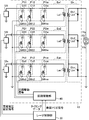
- FIG. 2 shows the electric circuit of the pulse power module 13 shown in FIG.
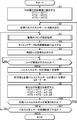
- FIG. 3 is a flowchart showing a process for the laser control unit 30 to control the pulse energy of the pulsed laser beam.
- FIG. 4 is a flowchart for explaining the subroutine of the drive timing setting process in S3 of FIG.
- FIG. 5 is a time chart illustrating waveform control by setting the drive timing.
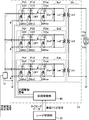
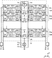
- FIG. 6 shows the electric circuit of the pulse power module 13 according to the first embodiment of the present disclosure. In the same electric circuit as in FIG. 6, FIG.
- FIG. 7 shows the flow of current when the condenser Cij is charged by the charger 12 with a broken arrow.
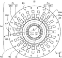
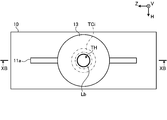
- FIG. 8A is a plan view showing a second embodiment in which the pulse power module 13 is mounted on a circular substrate.
- FIG. 8B schematically shows a cross section in line VIIIB-A-VIIIB of FIG. 8A.
- FIG. 9 schematically shows the structure of the pulse power module 13 according to the third embodiment, which is composed of n primary side electric circuits Ea1 to Ean and n transcores TC1 to TCn.
- FIG. 10A is a plan view showing a fourth embodiment in which the pulse power module 13 is arranged in the laser chamber 10.
- FIG. 10B is a cross-sectional view taken along the line XB-XB of FIG. 10A.
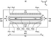
- FIG. 11A is a plan view showing a state in which the pulse power module 13 according to the fifth embodiment of the present disclosure is arranged in the laser chamber 10.
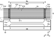
- FIG. 11B is a cross-sectional view taken along the line XIB-XIB of FIG. 11A.
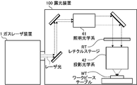
- FIG. 12 schematically shows the configuration of the exposure device 100 connected to the gas laser device 1.
- Pulse power module in which n primary side electric circuits are stacked. Pulse power module placed in the laser chamber 6. Pulse power module with a long transformer core in the Z direction 6.1 Trans core configuration 6.2 Secondary coil configuration 6.3 m pulse generator configuration 6.4 Action 7. Other
- FIG. 1 schematically shows the configuration of the gas laser device 1 according to the comparative example.
- the internal configuration of the gas laser apparatus 1 as viewed from a direction substantially perpendicular to the discharge direction between the pair of discharge electrodes 11a and 11b and substantially perpendicular to the traveling direction of the laser beam output from the output coupling mirror 15. It is shown.
- the traveling direction of the laser beam output from the output coupling mirror 15 is defined as the + Z direction.
- the discharge direction between the discharge electrodes 11a and 11b is defined as the + V direction or the ⁇ V direction.
- the direction perpendicular to both of these is defined as the + H direction or the ⁇ H direction.
- the Z direction corresponds to the first direction in the present disclosure.
- the H direction corresponds to the second direction in the present disclosure.
- the -V direction almost coincides with the direction of gravity.
- the ⁇ V direction corresponds to the third direction in the present disclosure.
- the + V direction corresponds to the fourth direction in the present disclosure.
- the gas laser device 1 is used together with the exposure device 100.
- the laser beam output from the gas laser apparatus 1 is incident on the exposure apparatus 100.
- the exposure apparatus 100 includes an exposure apparatus control unit 110.
- the exposure apparatus control unit 110 is configured to control the exposure apparatus 100.
- the exposure apparatus control unit 110 is configured to transmit setting data of the target pulse energy Et and an oscillation trigger signal to the laser control unit 30 included in the gas laser apparatus 1.
- the gas laser device 1 includes a laser chamber 10, a charger 12, a pulse power module 13, a narrow band module 14, an output coupling mirror 15, an energy monitor 17, a cross flow fan 21, a motor 22, and a laser.
- the control unit 30 and the like are included.
- the gas laser device 1 is, for example, an excimer laser device.
- the laser control unit 30 controls the control of the entire gas laser device 1.
- the laser chamber 10 is arranged in the optical path of the laser resonator composed of the narrow band module 14 and the output coupling mirror 15.
- the laser chamber 10 is provided with two windows 10a and 10b.
- the laser chamber 10 houses the discharge electrodes 11a and 11b.
- the laser chamber 10 houses a laser gas as a laser medium.
- the laser gas includes, for example, argon gas, fluorine gas, and neon gas.
- the laser gas includes, for example, krypton gas, fluorine gas, and neon gas.
- An opening is formed in a part of the laser chamber 10, and this opening is closed by the electrically insulating portion 29.
- the electrically insulating portion 29 supports the discharge electrode 11a.
- a plurality of conductive portions 29a are embedded in the electrically insulating portion 29. Each of the conductive portions 29a is electrically connected to the discharge electrode 11a.
- a return plate 10c is arranged inside the laser chamber 10.
- the conductive member of the laser chamber 10 is electrically connected to the return plate 10c.
- the return plate 10c supports the discharge electrode 11b.
- the return plate 10c is electrically connected to the discharge electrode 11b.
- the cross flow fan 21 is arranged inside the laser chamber 10.
- the rotation axis of the cross flow fan 21 is connected to a motor 22 arranged outside the laser chamber 10.
- the motor 22 rotates the cross flow fan 21.
- the laser gas circulates inside the laser chamber 10.
- the charger 12 holds electrical energy for supplying to the pulse power module 13.
- the pulse power module 13 includes a switch SW.
- the charger 12 is connected to the pulse power module 13.
- the pulse power module 13 is connected to the discharge electrode 11a via the conductive portion 29a.
- the narrow band module 14 includes wavelength selection elements such as a prism 14a and a grating 14b.
- a high reflection mirror may be used instead of the narrow band module 14.
- the output coupling mirror 15 is composed of a partially reflective mirror.
- the energy monitor 17 includes a beam splitter 17a, a condenser lens 17b, and an optical sensor 17c.
- the beam splitter 17a is arranged in the optical path of the laser beam output from the output coupling mirror 15.
- the beam splitter 17a is configured to transmit a part of the laser beam output from the output coupling mirror 15 toward the exposure apparatus 100 with a high transmission rate and to reflect the other part.
- the condenser lens 17b and the optical sensor 17c are arranged in the optical path of the laser beam reflected by the beam splitter 17a.
- the laser control unit 30 receives the setting data of the target pulse energy Et and the oscillation trigger signal from the exposure device control unit 110.
- the laser control unit 30 transmits a charge voltage setting signal to the charger 12 based on the target pulse energy Et setting data received from the exposure device control unit 110. Further, the laser control unit 30 transmits the oscillation trigger signal received from the exposure device control unit 110 to the pulse power module 13.
- the pulse power module 13 When the pulse power module 13 receives the oscillation trigger signal from the laser control unit 30, it generates a pulsed high voltage from the electric energy charged in the charger 12, and applies this high voltage between the discharge electrodes 11a and 11b. To do.
- the light generated in the laser chamber 10 is emitted to the outside of the laser chamber 10 through the windows 10a and 10b.
- the light emitted from the window 10a of the laser chamber 10 has its beam width expanded by the prism 14a and enters the grating 14b.
- the light incident on the grating 14b from the prism 14a is reflected by the plurality of grooves of the grating 14b and diffracted in a direction corresponding to the wavelength of the light.
- the grating 14b is arranged in a retrow so that the incident angle of the light incident on the grating 14b from the prism 14a coincides with the diffraction angle of the diffracted light having a desired wavelength. As a result, light near the desired wavelength is returned to the laser chamber 10 via the prism 14a.
- the output coupling mirror 15 transmits a part of the light emitted from the window 10b of the laser chamber 10 and outputs the light, reflects the other part, and returns the light to the laser chamber 10.
- the light emitted from the laser chamber 10 reciprocates between the narrow band module 14 and the output coupling mirror 15. This light is amplified each time it passes through the discharge space between the discharge electrodes 11a and 11b. Further, this light is narrowed each time it is folded back by the narrowing module 14. The light oscillated by the laser and narrowed in band is output as laser light from the output coupling mirror 15.
- the condenser lens 17b included in the energy monitor 17 focuses the laser beam reflected by the beam splitter 17a on the optical sensor 17c.
- the optical sensor 17c transmits an electric signal corresponding to the pulse energy of the laser beam focused by the condensing lens 17b to the laser control unit 30 as measurement data.
- the laser control unit 30 receives measurement data from the energy monitor 17.
- the laser control unit 30 feedback-controls the charging voltage set in the charger 12 based on the pulse energy measurement data received from the energy monitor 17 and the target pulse energy Et setting data received from the exposure device control unit 110. To do.
- FIG. 2 shows the electric circuit of the pulse power module 13 shown in FIG.
- the pulse power module 13 in the comparative example includes n primary side electric circuits Ea1 to Ean, a secondary side electric circuit Eb, and a circuit drive unit 60.
- the pulse power module 13 is a pulse compression circuit configured by an LTD (Linear Transformer Driver).
- LTD Linear Transformer Driver
- the pulse power module 13 is connected to the laser control unit 30 by a signal line.
- the charger 12 described with reference to FIG. 1 is composed of n chargers 121 to 12n as shown in FIG.
- the n chargers 121 to 12n are connected to n primary side electric circuits Ea1 to Ean, respectively.
- n is a natural number of 2 or more, for example, a natural number in the range of 15 to 30.
- Each of the n chargers 121 to 12n, each charger 12i, is a DC power supply device.
- i is an arbitrary natural number of 1 or more and n or less.
- the symbols of n constituent elements X may be numbered 1 to n to distinguish the n constituent elements X1 to Xn from each other.
- the reference numeral Xi may be used instead of one of the n constituent elements Y1 to Yn different from the n constituent elements X1 to Xn.
- the constituent elements Xi and the constituent elements Yi have a corresponding relationship with each other.
- the n primary side electric circuits Ea1 to Ean one terminal is connected to the reference potential and the other terminal is connected to the charger 12i. That is, the n primary side electric circuits Ea1 to Ean are connected in parallel with each other.
- the reference potential is, for example, the ground potential.
- the n chargers 121 to 12n are connected to the laser control unit 30 by a signal line.
- the primary side electric circuit Eai includes a primary side coil Lai and m pulse generating units Pi1 to Pim. That is, the n primary side electric circuits Ea1 to Ean include n primary side coils La1 to Lan and n ⁇ m pulse generators represented by the reference numerals Pij, respectively.
- m is a natural number of 2 or more, for example, a natural number in the range of 15 to 30.
- j is an arbitrary natural number of 1 or more and m or less.
- the symbols of m component Xs may be numbered 1 to m to distinguish m components X1 to Xm from each other.
- the reference numeral Xj may be used instead.
- the codes of the n ⁇ m component X may be numbered 11 to nm to distinguish the n ⁇ m component X11 to Xnm from each other.
- the reference numeral Xij may be used instead.
- the pulse generating unit Pij includes a capacitor Cij and a switch SWij.
- the capacitor Cij and the switch SWij are connected in series.
- m pulse generating units Pi1 to Pim are connected in parallel with each other.
- the primary side coil Lai is connected in parallel to m pulse generating units Pi1 to Pim.
- the terminal located on the switch SWij side is connected to the reference potential, and the terminal located on the capacitor Cij side is connected to the output terminal of the charger 12i.
- the switch SWij is composed of, for example, a MOSFET (metal-oxide-semiconductor field-effect transistor).
- the drain terminal of the MOSFET constituting the switch SWij is connected to one terminal of the capacitor Cij.
- the source terminal of the MOSFET is connected to the reference potential.
- the gate terminal of the MOSFET is connected to the circuit drive unit 60 by a signal line.
- N signal lines are connected to the circuit drive unit 60.
- the n signal lines are connected to n primary side electric circuits Ea1 to Ean, respectively.
- Each of the n signal lines is branched into m signal lines.
- the m signal lines are connected to m switches SWi1 to SWim included in the primary side electric circuit Eai, respectively. That is, m signal lines are connected to m gate terminals of m MOSFETs, respectively.
- the secondary side electric circuit Eb includes n secondary side coils Lb1 to Lbn and n diodes Db1 to Dbn.
- the n secondary coil Lb1 to Lbn are connected in series with each other.
- the n diodes Db1 to Dbn are connected in parallel to the n secondary coils Lb1 to Lbn, respectively.
- a transformer is composed of n primary side coils La1 to Lan, n secondary side coils Lb1 to Lbn, and n transformer cores TC1 to TCn (see FIGS. 8A to 11B). The n transcores TC1 to TCn and each transcore TCi will be described later.
- the laser control unit 30 transmits a charging voltage setting signal to n chargers 121 to 12n.
- the charging voltages ⁇ V set in each of the n chargers 121 to 12n are, for example, substantially the same values as each other.
- the charging voltage ⁇ V is, for example, a voltage that becomes a positive potential with respect to the reference potential.
- the charging voltage ⁇ V may be, for example, about 1 kV.
- Each of the n chargers 121 to 12n, each of the chargers 12i charges the m capacitors Ci1 to Cim included in the primary side electric circuit Eai with a charging voltage ⁇ V.
- the laser control unit 30 outputs timing data and an oscillation trigger signal to the circuit drive unit 60.
- the timing data is data that determines the drive timing of each of the n primary side electric circuits Ea1 to Ean. Even if the timing data includes information that determines which of the n primary side electric circuits Ea1 to Ean is driven and which primary side electric circuit is not driven. Good.
- the number and breakdown of the driven primary side electric circuits among the n primary side electric circuits Ea1 to Ean are determined based on the target pulse energy Et of the pulse laser light output from the gas laser device 1. May be good.
- the circuit drive unit 60 transmits a circuit drive signal to the primary side electric circuit Eai based on the timing data and the oscillation trigger signal.
- the circuit drive signal is input to the m switches SWi1 to SWim included in the primary side electric circuit Eai almost at the same time.
- a pulsed current flows from the m capacitors Ci1 to Cim almost at the same time.
- the pulsed current flowing from the m capacitors Ci1 to Cim flows into the primary coil Lai. In the primary coil Lai, the pulsed current flows from the upper side to the lower side in FIG.
- a pulsed current flowing through the primary coil Lai generates a magnetic flux in the transcore TCi described later, and the generation of this magnetic flux causes an induced electromotive force in the secondary coil Lbi.
- a pulsed voltage is applied between the pair of discharge electrodes 11a and 11b.
- the induced electromotive force generated in the secondary side coil Lbi is substantially the same as the charging voltage ⁇ V of the charger 12i. If the number of primary side electric circuits driven at the same time among the n primary side electric circuits Ea1 to Ean is large, the induced electromotive force of the n secondary side coils Lb1 to Lbn is generated at the same time 2 The number of next-side coils increases.
- the voltage applied between the pair of discharge electrodes 11a and 11b is i ⁇ ⁇ V. Will be.
- the n-1 secondary side coils Lb2 to Lbn At the same time, an induced electromotive force is generated.
- a large pulsed current also flows through the remaining secondary side coils Lb1 connected in series to the n-1 secondary side coils Lb2 to Lbn.
- a pulsed current flowing through the secondary coil Lb1 generates a magnetic flux in the transcore TC1 described later, and the generation of this magnetic flux causes an induced electromotive force to be generated in the primary coil La1.
- a diode Db1 is provided in order to suppress damage to the switches SW11 to SW1m and the charger 121. That is, even if an induced electromotive force is generated in any of the n-1 secondary side coils Lb2 to Lbn, the current flows through the diode Db1, so that the current flow through the secondary side coil Lb1 is suppressed.
- FIG. 3 is a flowchart showing a process for the laser control unit 30 to control the pulse energy of the pulsed laser beam.
- the laser control unit 30 sets the applied voltages V (T1), V (T2), and V (T3) between the pair of discharge electrodes 11a and 11b as follows.
- V (T1) V0 (T1)
- V (T2) V0 (T2)
- V (T3) V0 (T3)
- the applied voltages V (T1), V (T2), and V (T3) are the applied voltages between the pair of discharge electrodes 11a and 11b at the timings delayed by the time T1, T2, and T3 from the oscillation trigger signal, respectively.
- V0 (T1), V0 (T2), and V0 (T3) are initial values of the applied voltages V (T1), V (T2), and V (T3), respectively.
- Times T1 to T3 have the relationship of the following equation.
- T1 ⁇ T2 ⁇ T3 The time T3 is a time within a time during which the discharge required to output the pulsed laser beam having the desired pulse energy can be continued.
- the one having the maximum absolute value is, for example, the applied voltage V (T1).
- the applied voltage V (T1) is set to a voltage at which the laser gas between the pair of discharge electrodes 11a and 11b can at least break the insulation and start the main discharge.
- the applied voltages V (T2) and V (T3) are set to voltages at which the main discharge initiated by the applied voltage V (T1) can be continued.
- the laser control unit 30 reads the target pulse energy Et set by the exposure device control unit 110.
- the laser control unit 30 performs the drive timing setting process.
- the drive timing setting process is a process of setting each drive timing of the n primary side electric circuits Ea1 to Ean and creating timing data. The details of the drive timing setting process will be described later with reference to FIG.
- the laser control unit 30 outputs the timing data created in S3 to the circuit drive unit 60.
- the laser control unit 30 outputs the oscillation trigger signal received from the exposure device control unit 110 to the circuit drive unit 60.
- the circuit drive unit 60 controls the drive of n primary side electric circuits Ea1 to Ean based on the timing data and the oscillation trigger signal. Specifically, the circuit drive unit 60 delays the primary side electric circuit to be driven among the n primary side electric circuits Ea1 to Ean by the time T1, T2, and T3 from the oscillation trigger signal, respectively. It may be driven at the timing. The number of primary side electric circuits to be driven among the n primary side electric circuits Ea1 to Ean and their breakdown will be described later with reference to FIG.
- the laser control unit 30 determines whether or not laser oscillation has been performed. If the laser oscillation is not performed, the laser control unit 30 waits until the laser oscillation is performed. When the laser oscillation is performed, the laser control unit 30 shifts to S7.
- the laser control unit 30 acquires the measured value E of the pulse energy measured by the energy monitor 17.
- the laser control unit 30 calculates the difference ⁇ E between the measured value E of the pulse energy and the target pulse energy Et.
- the laser control unit 30 sets new applied voltages V (T1), V (T2), and V (T3) so that the difference ⁇ E approaches 0.
- the new applied voltages V (T1), V (T2), and V (T3) are set using the following equation.
- V (T1) V (T1) + ⁇ 1 ⁇ ⁇ E
- V (T2) V (T2) + ⁇ 2 ⁇ ⁇ E
- V (T3) V (T3) + ⁇ 3 ⁇ ⁇ E
- ⁇ 1, ⁇ 2, and ⁇ 3 on the right side may be proportional constants obtained in advance by experiments or the like.
- the laser control unit 30 determines whether or not the target pulse energy Et has been changed.
- the exposure apparatus control unit 110 may change the target pulse energy Et.
- the exposure device control unit 110 outputs the changed target pulse energy Et setting data to the laser control unit 30.
- the laser control unit 30 returns to S2.
- the target pulse energy Et is not changed (S10: NO)
- the laser control unit 30 shifts to S11.
- the laser control unit 30 determines whether or not to end the process of controlling the pulse energy of the pulsed laser beam.
- the laser control unit 30 returns to S3.
- the laser control unit 30 ends the process of controlling the pulse energy of the pulsed laser beam (S11: YES)
- the laser control unit 30 ends the process of this flowchart.
- FIG. 4 is a flowchart for explaining a subroutine of the drive timing setting process in S3 of FIG.
- the laser control unit 30 sets the identification number i to 1.
- the identification number i when the identification number i is set, it is assumed that one of the n primary side electric circuits Ea1 to Ean is identified.
- the identification number i when the identification number i is set, one charger 12i corresponding to the primary side electric circuit Eai is also identified.
- the laser control unit 30 sets the drive timing of the primary side electric circuit Eai while counting up the identification number i.
- the laser control unit 30 is the total value of the charging voltages by the i chargers 121 to 12i identified by the identification numbers 1 to i. Is determined to be equal to or lower than the applied voltage V (T1).
- the applied voltage V (T1) is a value set in S1 of FIG. 3 as an applied voltage between the pair of discharge electrodes 11a and 11b at time T1.
- the total value of the charging voltage by the i chargers 121 to 12i is represented by i ⁇ ⁇ V. Therefore, the determination of S302 is performed depending on whether or not the following conditions are satisfied. i ⁇ ⁇ V ⁇ V (T1)
- the laser control unit 30 shifts to S305 when the total value i ⁇ ⁇ V of the charging voltage is not equal to or less than the applied voltage V (T1) (S302: NO). When the total value i ⁇ ⁇ V of the charging voltage is equal to or less than the applied voltage V (T1) (S302: YES), the laser control unit 30 shifts to S303.
- the laser control unit 30 sets the drive timing of the primary side electric circuit Eai identified by the identification number i to the time T1.
- the laser control unit 30 adds 1 to the value of the identification number i to update the value of the identification number i. After that, the laser control unit 30 returns to S302.
- a first threshold value k 1 sets the value of the current identification number i.
- the first threshold value k 1 is smaller than the identification number 1 ⁇ k 1 k 1 that is identified by -1 -1 primary electric circuit Ea1 ⁇ Eak 1 -1 at a timing delayed by the time T1 from the oscillation trigger signal This is the primary side electric circuit to be driven.
- the primary side electric circuits Eak 1 to Ean identified by the identification numbers k 1 to n having the first threshold value k 1 or more are primary side electric circuits that are not to be driven at a timing delayed by a time T1 from the oscillation trigger signal. is there.
- k 1 when -1 is driven simultaneously primary electric circuit Ea1 ⁇ Eak 1 -1, while a voltage close to the applied voltage V (T1) of the pair of discharge electrodes 11a and 11b Can be applied to.
- the laser control unit 30 is identified by identification numbers k 1 to i i-k 1 + 1 charger 12k 1 to 12i. It is determined whether or not the total value of the charging voltage according to the above is equal to or less than the applied voltage V (T2).
- the applied voltage V (T2) is a value set in S1 as an applied voltage between the pair of discharge electrodes 11a and 11b at time T2.
- the total value of the charging voltage by the i-k 1 + 1 charger 12k 1 to 12i is represented by (i-k 1 + 1) ⁇ ⁇ V. Therefore, the determination of S306 is performed depending on whether or not the following conditions are satisfied. (Ik 1 + 1) ⁇ ⁇ V ⁇ V (T2)
- the laser control unit 30 shifts to S309 when the total value (i-k 1 + 1) ⁇ ⁇ V of the charging voltage is not equal to or less than the applied voltage V (T2) (S306: NO). When the total value (i-k 1 + 1) ⁇ ⁇ V of the charging voltage is equal to or less than the applied voltage V (T2) (S306: YES), the laser control unit 30 shifts to S307.
- the laser control unit 30 sets the drive timing of the primary side electric circuit Eai identified by the identification number i to the time T2. In S308, the laser control unit 30 adds 1 to the value of the identification number i to update the value of the identification number i. After that, the laser control unit 30 returns to S306.
- the laser control unit 30 sets the second threshold value k 2 to the value of the current identification number i.
- the first threshold value k 1 or the second threshold value k 2 is smaller than the identification number k 1 ⁇ k 2 k 2 -k 1 single primary identified by -1 electrical circuits Eak 1 ⁇ Eak 2 -1 is This is the primary side electric circuit to be driven at a timing delayed by the time T2 from the oscillation trigger signal.
- Other identification numbers 1 ⁇ k 1 -1 and primary electrical circuit which is identified by k 2 ⁇ n Ea1 ⁇ Eak 1 -1 and Eak 2 ⁇ Ean may drive at a timing delayed by the time T2 from the oscillation trigger signal It is a primary side electric circuit that is not a target.
- k 2 -k 1 one primary electric circuit Eak 1 ⁇ Eak 2 -1 simultaneously when driving, a voltage close to the applied voltage V (T2) of the pair discharge electrodes 11a and 11b Can be applied between.
- the laser control unit 30 uses i-k 2 + 1 chargers 12k 2 to 12i identified by identification numbers k 2 to i. It is determined whether or not the total value of the charging voltage according to the above is equal to or less than the applied voltage V (T3).
- the applied voltage V (T3) is a value set in S1 as an applied voltage between the pair of discharge electrodes 11a and 11b at time T3.
- the total value of the charging voltage by ik 2 + 1 chargers 12k 2 to 12i is represented by (i-k 2 + 1) ⁇ ⁇ V. Therefore, the determination of S310 is performed depending on whether or not the following conditions are satisfied. (Ik 2 +1) ⁇ ⁇ V ⁇ V (T3)
- the laser control unit 30 shifts to S313 when the total value (i-k 2 + 1) ⁇ ⁇ V of the charging voltage is not equal to or less than the applied voltage V (T3) (S310: NO).
- the laser control unit 30 shifts to S311.
- the laser control unit 30 sets the drive timing of the primary side electric circuit Eai identified by the identification number i to the time T3.
- the laser control unit 30 adds 1 to the value of the identification number i to update the value of the identification number i. After that, the laser control unit 30 returns to S310.
- a third threshold value k 3 it is set to the current value of the identification number i.
- Third threshold k 3 is smaller than the identification number k 2 ⁇ k 3 k 3 are identified by -1 -k 2 pieces of primary electric circuit Eak 2 ⁇ Eak 3 -1 in the second threshold value k 2 or more, This is the primary side electric circuit to be driven at a timing delayed by the time T3 from the oscillation trigger signal.
- Other identification numbers 1 ⁇ k 2 -1 and k 3 1 primary electrical circuit identified in ⁇ n Ea1 ⁇ Eak 2 -1 and Eak 3 ⁇ Ean may drive at a timing delayed by a time T3 from the oscillation trigger signal It is a primary side electric circuit that is not a target.
- k 3 -k 2 pieces of primary electric circuit Eak 2 ⁇ Eak 3 -1 simultaneously when driving, a voltage close to the applied voltage V (T3) of the pair discharge electrodes 11a and 11b Can be applied between.
- the laser control unit 30 sets the switches SWi1 to SWim included in the primary side electric circuit Eai of the identification number i to off. That is, the primary side electric circuit Eai of the identification number i is set to the primary side electric circuit that is not the target to be driven.
- the laser control unit 30 adds 1 to the value of the identification number i to update the value of the identification number i.
- the laser control unit 30 determines whether or not the current value of the identification number i is larger than the number n of the primary side electric circuits Ea1 to Ean. When the current value of the identification number i is the number n or less of the primary side electric circuits Ea1 to Ean (S316: NO), the laser control unit 30 returns to S314. When the current value of the identification number i is larger than the number n of the primary side electric circuits Ea1 to Ean (S316: YES), the laser control unit 30 ends the process of this flowchart and shifts to S4 of FIG. Timing data is generated as described above.
- FIG. 5 is a time chart for explaining waveform control by setting the drive timing.
- the horizontal axis of FIG. 5 indicates the time T.
- the vertical axis of FIG. 5 shows the strength of a signal such as voltage V.
- the laser control unit 30 outputs an oscillation trigger signal to the circuit drive unit 60.
- the laser control unit 30 outputs timing data to the circuit drive unit 60 in addition to the oscillation trigger signal.
- Circuit drive section 60 the primary side electric circuit Ea1 ⁇ Eak 1 -1 identified by identification numbers 1 ⁇ k 1 -1, and transmits the circuit driving signal at a timing delayed by the time T1 from the oscillation trigger signal.
- the switch SWij is turned on included in the primary electrical circuit Ea1 ⁇ Eak 1 -1.
- Circuit drive section 60, the primary side electric circuit Eak 1 ⁇ Eak 2 -1 identified by identification numbers k 1 ⁇ k 2 -1 transmits a circuit driving signal at a timing delayed by the time T2 from the oscillation trigger signal .
- the switch SWij is turned on included in the primary electrical circuit Eak 1 ⁇ Eak 2 -1.
- Circuit drive section 60 the primary side electric circuit Eak 2 ⁇ Eak 3 -1 identified by the identification number k 2 ⁇ k 3 -1, and transmits the circuit driving signal at a timing delayed by a time T3 from the oscillation trigger signal .
- the switch SWij is turned on included in the primary electrical circuit Eak 2 ⁇ Eak 3 -1.
- the circuit drive unit 60 keeps the switch SWij included in the primary side electric circuits Eak 3 to Ean identified by the identification numbers k 3 to n off.
- each ⁇ Eak 3 -1 primary electrical circuit EAI the switch SWij is turned on, a pulse-like voltage having a peak value of the charging voltage ⁇ V is the primary coil Lai ends Is applied to.
- the primary side electric circuits Eai of each of the primary side electric circuits Eak 3 to Ean are maintained in an undriven state.
- Voltage Vs (T1) corresponds to a voltage which is the sum of voltages respectively applied to the primary coil La1 ⁇ Lak 1 -1 in k 1 -1 single primary electric circuit Ea1 ⁇ Eak 1 -1. Peak value of the voltage Vs (T1) becomes (k 1 -1) ⁇ ⁇ V.
- Voltage Vs (T2) is equivalent to k 2 -k 1 one primary electric circuit Eak 1 ⁇ Eak 2 respectively primary coils Lak in -1 1 ⁇ Lak 2 -1 voltage which is the sum of the voltage applied to the To do.
- the peak value of the voltage Vs (T2) is (k 2- k 1 ) ⁇ ⁇ V.
- Voltage Vs (T3) is equivalent to k 3 -k 2 pieces of primary electric circuit Eak 2 ⁇ Eak 3 voltage which is the sum of voltages applied to the primary coil Lak 2 ⁇ Lak 3 -1 In -1 To do.
- the peak value of the voltage Vs (T3) is (k 3- k 2 ) ⁇ ⁇ V.
- Primary number k 1 -1 of the electric circuit Ea1 ⁇ Eak 1 -1 driven at the timing of time T1 the number k of the primary electric circuit Eak 1 ⁇ Eak 2 -1 driven at the timing of time T2 more than 2 -k 1 is desirable.
- Primary number k 1 -1 of the electric circuit Ea1 ⁇ Eak 1 -1 driven at the timing of time T1 the number k of the primary electric circuit Eak 2 ⁇ Eak 3 -1 driven at the timing of time T3 More than 3- k 2 is desirable.
- the absolute value of the peak value of the voltage Vs (T1) that occurs in k 1 -1 single secondary coil Lb1 ⁇ Lbk 1 -1 is, k 2 -k 1 single secondary coil Lbk 1 ⁇ Lbk It is higher than the absolute value of the peak value of the voltage Vs (T2) generated in 2-1.
- k 1 the absolute value of the peak value of -1 of the secondary coil Lb1 ⁇ Lbk 1 voltage occurring at -1 Vs (T1) is, k 3 -k 2 pieces of the secondary coil Lbk 2 ⁇ Lbk 3 -1 It becomes higher than the absolute value of the peak value of the voltage Vs (T3) generated in.
- the pulse waveform of the voltage Vr applied between the pair of discharge electrodes 11a and 11b is a waveform substantially similar to the waveform of the voltage Vs (T1) until just before the insulation failure occurs.
- the voltage Vr rapidly approaches 0.
- the voltages Vs (T2) and Vs (T3) are applied, the voltage Vr does not become 0 and is maintained at a voltage at which the main discharge can be continued.
- the current I flowing through the secondary side electric circuit Eb peaks. After that, while the main discharge is continued, a current lower than the peak current flows through the secondary side electric circuit Eb. By this main discharge, the laser gas is excited to emit light, and the pulse laser light is output from the gas laser device 1.
- the pulse waveform of the pulsed laser beam has a substantially similar shape to the pulse waveform of the current flowing through the secondary side electric circuit Eb. By setting the drive timing as described above, the waveform of the pulsed laser beam is controlled.
- n diodes Da1 to Dan are arranged in n primary side electric circuits Ea1 to Ean, respectively.
- the output inductance of the pulse power module 13 can be reduced, and pulsed laser light having a desired pulse energy can be output.
- FIG. 6 shows the electric circuit of the pulse power module 13 in the first embodiment of the present disclosure.
- the pulse power module 13 corresponds to the high voltage pulse generator of the present disclosure.
- the output terminal of the charger 12i is connected to the terminal located on the capacitor Cij side.
- the output terminal of the charger 12 is connected between the capacitor Cij and the switch SWij.
- the charger 12 may be a common charger connected to n primary side electric circuits Ea1 to Ean.
- the terminal located on the switch SWij side is connected to the reference potential.
- n diodes Db1 to Dbn described with reference to FIG. 2 may not be provided in the first embodiment.
- n diodes Da1 to Dan are arranged in each of the n primary side electric circuits Ea1 to Ean.
- the n diodes Da1 to Dan are connected in parallel to the n primary coil La1 to Lan included in the n primary side electric circuits Ea1 to Ean, respectively. That is, the diode Dai is connected in parallel to the primary side coil Lai included in the primary side electric circuit Eai.
- the diode Dai is connected so that the cathode side has a reference potential. That is, the anode of the diode Dai has substantially the same potential as the terminals located on the capacitor Cij side among the terminals at both ends of the pulse generating portion Pij.
- the cathode of the diode Dai has substantially the same potential as the terminals located on the switch SWij side among the terminals at both ends of the pulse generating portion Pij.
- the charger 12 charges m capacitors Ci1 to Cim included in the primary side electric circuit Eai with a charging voltage ⁇ V. After that, when the m switches SWi1 to SWim included in the primary side electric circuit Eai are turned from the off state to the on state almost at the same time, a pulsed current flows from the m capacitors Ci1 to Cim almost at the same time. Since the pulsed current flowing from the m capacitors Ci1 to Cim has a reverse bias with respect to the diode Dai, the pulsed current flowing from the m capacitors Ci1 to Cim is suppressed from flowing to the diode Dai. To. The pulsed current flowing from the m capacitors Ci1 to Cim flows into the primary coil Lai.
- the pulsed current flows from the lower side to the upper side of FIG.
- a pulsed current flowing through the primary side coil Lai generates a magnetic flux in the transcore TCi described later, and the generation of this magnetic flux causes an induced electromotive force to be generated in the secondary side coil Lbi.
- a pulsed voltage is applied between the pair of discharge electrodes 11a and 11b. If the number of primary side electric circuits driven at the same time among the n primary side electric circuits Ea1 to Ean is large, the induced electromotive force of the n secondary side coils Lb1 to Lbn is generated at the same time 2 The number of next-side coils increases.
- FIG. 6 the direction of the current when the primary side electric circuit Ea1 is not driven and the remaining n-1 primary side electric circuits Ea2 to Ean are driven is indicated by a broken line arrow.
- induced electromotive force is generated simultaneously in n-1 secondary side coils Lb2 to Lbn.
- a large pulsed current also flows through the remaining secondary coil Lb1 connected in series to the n-1 secondary coil Lb2 to Lbn.
- a pulsed current flowing through the secondary coil Lb1 generates a magnetic flux in the transcore TC1 described later, and the generation of this magnetic flux causes an induced electromotive force to be generated in the primary coil La1.
- FIG. 7 shows the current flow when the capacitor Cij is charged by the charger 12 in the same electric circuit as in FIG. 6 with a broken line arrow. At this time, all switches SWij are in the off state.
- a current flows into the terminal on the switch SWij side of the condenser Cij to charge the condenser Cij.
- a negative charge flows into the terminal on the opposite side of the capacitor Cij from the switch SWij. That is, a current flows out from the terminal on the opposite side of the capacitor Cij to the switch SWij.
- the current flowing out from the terminal opposite to the switch SWij of the capacitor Cij is discharged to the reference potential through the diode Dai.
- the secondary side electric circuit Eb can be simplified. As a result, the output inductance of the pulse power module 13 can be reduced. Further, for example, when the primary side electric circuit Ea1 is not driven and the remaining n-1 primary side electric circuits Ea2 to Ean are driven, damage to the switches SW11 to SW1m and the charger 12 is suppressed. Can be done.
- the condenser Cij since the current flows through the diode Dai when charging the condenser Cij, the condenser Cij can be charged efficiently. Further, since it is possible to suppress the flow of current through the primary coil Lai during charging, it is possible to suppress the generation of magnetic flux in the transcore TCi and suppress the energy loss.
- the first embodiment is the same as the above-mentioned comparative example.
- FIG. 8A is a plan view showing a second embodiment in which the pulse power module 13 is mounted on a circular substrate.
- FIG. 8B schematically shows a cross section in line VIIIB-A-VIIIB of FIG. 8A. However, in FIG. 8B, the side surface of the secondary coil Lb is shown instead of the cross section. 8A and 8B show one primary side electric circuit Eai among n primary side electric circuits Ea1 to Ean, one transcore TCi, and a part of the secondary side coil Lb. ..
- the transcore TCi has an annular shape. As shown in FIG. 8A, the magnetic circuit MC is formed along the annulus constituting the transcore TCi. As shown in FIG. 8B, the transcore TCi is located on the first surface PLi. The first plane PLi is parallel to the HZ plane. The magnetic circuit MC is formed along the first surface PLi.
- the secondary coil Lb is composed of a conductive member having a cylindrical shape. As shown in FIG. 8B, the secondary coil Lb has a through hole TH. The through hole TH penetrates the secondary coil Lb in the direction perpendicular to the first surface PLi.
- the primary side electric circuit Eai includes the substrates E1i and E2i and the components mounted on the substrate E1i.
- FIG. 8A the illustration of the substrate E2i is omitted. Both the substrates E1i and E2i are parallel to the first surface PLi.
- a transcore TCi is also mounted on the substrate E1i.
- the substrates E1i and E2i each include a conductive member. Both the substrates E1i and E2i are connected to the reference potential.
- the components mounted on the substrate E1i are a plurality of primary side coils Lai1 and Lai2, a plurality of diodes Dai1 and Dai2, m pulse generators Pi1 to Pim, and m switch drive units DRi1 to DRim. , A plurality of conductive members E3i and E4i.
- the components mounted on the substrate E1i are located between the substrates E1i and E2i together with the transcore TCi.
- the substrates E1i and E2i and the transcore TCi each have through holes, and the secondary coil Lb penetrates through these through holes in the direction perpendicular to the first surface PLi.
- the m pulse generating units Pi1 to Pim and the m switch driving units DRi1 to DRim are arranged radially around the transcore TCi.
- the plurality of primary side coils Lai1 and Lai2 each include a conductive member.
- the plurality of primary coil Lai1 and Lai2 and the plurality of diodes Dai1 and Dai2 are arranged in a space outside the secondary coil Lb and inside the transcore TCi. That is, the plurality of primary side coils Lai1 and Lai2 and the plurality of diodes Dai1 and Dai2 are arranged in the space between the secondary side coil Lb and the transcore TCi.
- Each of the plurality of diodes Dai1 and Dai2 is arranged in the vicinity of any one of the plurality of primary side coils Lai1 and Lai2.
- the plurality of diodes Dai1 and Dai2 are arranged around the secondary coil Lb at substantially equal intervals. By arranging the plurality of diodes Dai1 and Dai2 at substantially equal intervals, the bias of the current flowing through the plurality of diodes Dai1 and Dai2 is suppressed, and the load is concentrated on a part of the plurality of diodes Dai1 and Dai2. Can be suppressed.
- the plurality of primary side coils Lai1 and Lai2 and the plurality of diodes Dai1 and Dai2 are alternately arranged in the circumferential direction around the secondary side coil Lb.
- the arrangement of the elements will be described in detail with reference to FIG. 8B.
- the -V direction is the third direction.
- the + V direction is the fourth direction.
- the position and shape of the magnetic circuit MC shall match the position and shape of the closed curve along the center of the cross section of the transcore TCi.
- the region inside the magnetic circuit MC is defined as "inside the magnetic circuit”.
- the region outside the magnetic circuit MC in the plan view shown in FIG. 8A is defined as “outside the magnetic circuit”.
- first node N1 and the second node N2 are located on the third direction side of the first surface PLi and inside the magnetic circuit. It is assumed that the third node N3 is located on the third direction side of the first surface PLi and outside the magnetic circuit.
- the third node N3 is connected to the reference potential via the substrate E1i.
- the substrate E1i is located on the third direction side with respect to the first surface PLi, and connects the second node N2 and the third node N3.
- the substrate E1i has the function of the first conductive portion in the present disclosure.
- the fourth node N4 is located on the fourth direction side of the first surface PLi and inside the magnetic circuit. It is assumed that the fifth node N5 is located on the fourth direction side of the first surface PLi and outside the magnetic circuit.
- the fifth node N5 is connected to a reference potential via the substrate E2i.
- the substrate E2i is located on the fourth direction side with respect to the first surface PLi, and connects the fourth node N4 and the fifth node N5.
- the substrate E2i has the function of the second conductive portion in the present disclosure.
- the diode Dai2 is connected between the first node N1 and the second node N2.
- the anode of the diode Dai2 is connected to the first node N1 and the cathode of the diode Dai2 is connected to the second node N2.
- the same may apply to other diodes included in the primary side electric circuit Eai.
- the m pulse generators Pi1 to Pim are connected between the first node N1 and the third node N3.
- the m pulse generating units Pi1 to Pim include m capacitors Ci1 to Cim and m switches SWi1 to SWim. As shown in FIG. 8B, the capacitor Cij and the switch SWij are connected in series in each of the pulse generating units Pij of the m pulse generating units Pi1 to Pim.
- the m switches SWi1 to SWim are composed of m MOSFETs.
- the source terminals of the m MOSFETs constituting the m switches SWi1 to SWim are electrically connected to the substrate E1i at the third node N3 and connected to the reference potential via the substrate E1i.
- the gate terminals of the m MOSFETs constituting the m switches SWi1 to SWim are connected to the m switch drive units DRi1 to DRim via signal lines, respectively.
- the drain terminals of the m MOSFETs constituting the m switches SWi1 to SWim are electrically connected to one terminal of the m capacitors Ci1 to Cim, respectively.
- the output terminals of the charger 12 are electrically connected to the conductive members that connect the m switches SWi1 to SWim and the m capacitors Ci1 to Cim, respectively.
- the other terminals of the m capacitors Ci1 to Cim are electrically connected to the first node N1 via a conductive member.
- the conductive member that connects the m capacitors Ci1 to Cim and the first node N1 is located between the transcore TCi and the substrate E1i.
- An electrically insulating member (not shown) is arranged between the conductive member that connects the m capacitors Ci1 to Cim and the first node N1 and the substrate E1i.
- the primary side coil Lai1 is connected between the first node N1 and the fourth node N4.
- the primary side coil Lai1 includes a conductive portion.
- the conductive portion has, for example, a columnar shape. This conductive portion is located inside the magnetic circuit.
- One end of the conductive portion is electrically connected to the substrate E2i at the fourth node N4 and is connected to the reference potential via the substrate E2i.
- the other end of the conductive portion is connected to the first node N1.
- the conductive portion included in the primary side coil Lai1 corresponds to the third conductive portion in the present disclosure. Although not shown in FIG. 8B, the same may apply to other primary coil included in the primary electric circuit Eai.
- the plurality of conductive members E3i and E4i are electrically connected between the substrates E1i and E2i.
- the diode Dai2 is located inside the magnetic circuit.
- a current can flow to a reference potential via the diode Dai2 in a short current path.
- the m pulse generating units Pi1 to Pim are located outside the magnetic circuit.
- the space inside the magnetic circuit can be secured as an installation space for the primary side coil Lai1 and the secondary side coil Lb and the like. Therefore, the arrangement of the transcore TCi, the primary side coil Lai1, the secondary side coil Lb, and the like can be arranged so that magnetic energy can be efficiently transmitted.
- the second embodiment is the same as the first embodiment.
- FIG. 9 relates to a third embodiment composed of n primary side electric circuits Ea1 to Ean and n transcores TC1 to TCn.
- the structure of the pulse power module 13 is shown schematically.
- the n transcores TC1 to TCn are arranged side by side in the V direction.
- the n transcores TC1 to TCn are arranged so that their first surfaces PL1 to PLn are parallel to the HZ surface.
- the secondary coil Lb is arranged so as to penetrate each of the through holes of the n transcores TC1 to TCn.
- the upper end Lbu of the secondary side coil Lb is connected to the reference potential, and the lower end Lbb of the secondary side coil Lb is connected to the discharge electrode 11a.
- the "coil” is not limited to a conductive wire having a plurality of turns. Even a conductive member that only penetrates through the through hole of the transcore TCi corresponds to the coil of the present disclosure as long as it can transmit magnetic energy to and from the transcore TCi.
- the secondary side coil Lb corresponds to one in which n secondary side coils Lb1 to Lbn described with reference to FIG. 6 are connected in series.
- the n primary side electric circuits Ea1 to Ean are arranged side by side in the V direction.
- a plurality of primary side coils Lai1 and Lai2 included in each of the primary side electric circuits Eai of the n primary side electric circuits Ea1 to Ean are placed in the space inside the transcore TCi and outside the secondary side coil Lb. To position.
- the substrate E11 included in the primary side electric circuit Ea1 may include a conductive member common to the substrate E22 included in the primary side electric circuit Ea2 adjacent to the primary side electric circuit Ea1. That is, the substrate E1i included in the primary side electric circuit Eai may include a conductive member common to the substrate E2i + 1 included in the primary side electric circuit Eai + 1.
- i is a natural number from 1 to n-1.
- the substrate E1i itself may be shared with the substrate E2i + 1, and the substrate E2i + 1 may be omitted.
- the conductive member connecting the m capacitors Ci1 to Cim and the m switches SWi1 to SWim is charged.
- the output terminal of the vessel 12 is electrically connected.
- Resistor elements Ri1 to Rim may be connected between the charger 12 and the pulse generating units Pi1 to Pim of the primary side electric circuit Eai, respectively. Since the resistance elements Ri1 to Rim are connected, it is possible to suppress the flow of a large current from the charger 12 to the reference potential via the switches SWi1 to SWim when the switches SWi1 to SWim are turned on.
- the charger 12 may be a common charger connected to n primary side electric circuits Ea1 to Ean.
- the charger 12 charges the capacitors Cij included in the n primary side electric circuits Ea1 to Ean with a charging voltage ⁇ V.
- a pulsed current flows from the m capacitors C11 to C1m.
- the pulsed current flowing from the capacitors C11 to C1m flows into the primary coil La11 and La12.
- the pulsed current flows from the upper side to the lower side in FIG.
- a pulsed current flowing through the primary coil La11 and La12 causes a magnetic flux to be generated in the transcore TC1, and the generation of this magnetic flux causes an induced electromotive force to be generated in the secondary coil Lb.
- a pulsed voltage is applied between the pair of discharge electrodes 11a and 11b.
- the induced electromotive force generated in the secondary coil Lb by driving one primary electric circuit Ea1 is substantially the same as the charging voltage ⁇ V of the charger 12. Assuming that the number of the primary side electric circuits driven at the same time among the n primary side electric circuits Ea1 to Ean is i, the voltage applied between the pair of discharge electrodes 11a and 11b is i ⁇ ⁇ V. ..
- the third embodiment is the same as the second embodiment.
- FIG. 10A is a plan view showing a fourth embodiment in which the pulse power module 13 is arranged in the laser chamber 10.
- FIG. 10B is a cross-sectional view taken along the line XB-XB of FIG. 10A. In FIG. 10B, only the substrates E21 and E11 to E1n are shown for the n primary side electric circuits Ea1 to Ean, and the illustration of other circuit elements is omitted.
- n transcores TC1 to TCn are arranged side by side in the V direction.
- the n transcores TC1 to TCn are arranged so that their first planes PL1 to PLn are parallel to the HZ plane.
- the secondary coil Lb is arranged so as to penetrate all the through holes of the n transcores TC1 to TCn.
- the upper end Lbu of the secondary side coil Lb is connected to the reference potential, and the lower end Lbb of the secondary side coil Lb is connected to the discharge electrode 11a.
- the discharge electrode 11b is connected to the reference potential.
- the substrate E21 and n substrates E11 to E1n are arranged so as to sandwich n transcores TC1 to TCn.
- the pulsed high voltage generated by the pulse power module 13 can be directly applied to the discharge electrode 11a.
- the fourth embodiment is the same as the third embodiment.
- FIG. 11A having a transformer core elongated in the Z direction is a plan view showing a state in which the pulse power module 13 according to the fifth embodiment of the present disclosure is arranged in the laser chamber 10.
- FIG. 11B is a cross-sectional view taken along the line XIB-XIB of FIG. 11A.
- the laser chamber 10 has substantially the same shape as the substrates E11 to E1n included in the pulse power module 13 in the plan view shown in FIG. 11A. Therefore, only the pulse power module 13 is shown in FIG. 11A. Since the n transcores TC1 to TCn have the same configuration as each other and the n primary side electric circuits Ea1 to Ean have the same configuration as each other, in FIG. 11A, the components X1 to Xn are designated by the reference numerals Xi. I am substituting. In FIG. 11A, the illustration of the substrate E21 is omitted.
- each transcore TCi of the n transcores TC1 to TCn is such that the width Wz in the Z direction is larger than the width Wh in the H direction. ..
- the Z direction is the first direction parallel to the first planes PL1 to PLn.
- the H direction is a second direction parallel to the first planes PL1 to PLn and perpendicular to the first direction.
- the transcore TCi is arranged so that the Z direction, which is the longitudinal direction thereof, is parallel to the longitudinal direction of the pair of discharge electrodes 11a and 11b.
- the shape of the transcore TCi will be described in more detail.
- the transcore TCi includes first and second linear shape portions TCi1 and TCi2, and first and second curved portions TCi3 and TCi4.
- the first and second linear shape portions TCi1 and TCi2 are arranged along the Z direction.
- the first curved portion TCi3 connects the ends of the first and second linear shape portions TCi1 and TCi2 on the + Z direction side to each other.
- the second curved portion TCi4 connects the ends of the first and second linear shape portions TCi1 and TCi2 on the ⁇ Z direction side to each other.
- the transcore TCi has a race track shape.
- the shape of the transcore TCi is not limited to the above shape, and may be rectangular or elliptical.
- the width Wz of the transcore TCi in the Z direction is larger than the length DE of the pair of discharge electrodes 11a and 11b in the longitudinal direction (see FIG. 11B). It is desirable that the width Wh of the transcore TCi in the H direction is larger than the width of the pair of discharge electrodes 11a and 11b in the H direction.
- the secondary coil Lb has a tubular shape having a through hole TH in the direction perpendicular to the first surface PLi, and the width Wz1 in the Z direction is the width Wh1 in the H direction. It has a larger shape. It is desirable that the ratio of the width Wz1 of the secondary coil Lb in the Z direction to the length DE of the pair of discharge electrodes 11a and 11b in the longitudinal direction is 0.5 or more and 2 or less. It is more desirable that this ratio is 0.8 or more and 1.2 or less. This ratio is even more desirable to be about 1.
- the gap GAP (see FIG. 11B) between the transcore TCi and the secondary coil Lb is 5 mm or less. It is more desirable that the gap GAP is 1 mm or more and 3 mm or less.
- the m pulse generators are m 1 pulse generators Pia 1 to Piam 1 and m 2 pulse generators Pib1 to Pibm. 2 and are included. These pulse generators are located outside the magnetic circuit MC formed in the transcore TCi. m 1 pieces of pulse generator Pia1 ⁇ Piam 1, in -H direction than transformer core TCi, are arranged side by side in the Z direction. m 2 pieces of pulse generator Pib1 ⁇ Pibm 2, in than transformer core TCi + H direction, are arranged side by side in the Z direction.
- the m 1 pulse generating units Pia1 to Piam 1 and the m 2 pulse generating units Pib1 to Pibm 2 are located on opposite sides of the transcore TCi.
- FIG. 11A the illustration of m switch drive units DRi1 to DRim is omitted.
- Each of m 1 and m 2 is a natural number of 2 or more and m or less. Although m 1 and m 2 may be different numbers, it is desirable that they are the same number.
- m 1 pulse generating part Pia1 to Piam 1 have a first gap G1 with each other, and m 2 pulse generating parts Pib1 to Pibm 2 have a second gap G2 with each other. It is desirable that the first gap G1 and the second gap G2 are substantially equal.
- the primary coil Lai1 and Lai2 are arranged inside the transcore TCi and outside the secondary coil Lb, they are located between the transcore TCi and the primary coils Lai1 and Lai2. However, magnetic energy can be transmitted efficiently.
- the deviation of the pulse current in the longitudinal direction of the discharge electrode 11a Can be further reduced.
- the bias of the pulse current can be further reduced.
- the fifth embodiment is the same as the fourth embodiment.
- FIG. 12 schematically shows the configuration of the exposure apparatus 100 connected to the gas laser apparatus 1.
- the gas laser apparatus 1 generates laser light and outputs it to the exposure apparatus 100.
- the exposure apparatus 100 includes an illumination optical system 41 and a projection optical system 42.
- the illumination optical system 41 illuminates the reticle pattern of the reticle stage RT with the laser beam incident from the gas laser device 1.
- the projection optical system 42 reduces and projects the laser beam transmitted through the reticle to form an image on a workpiece (not shown) arranged on the workpiece table WT.
- the workpiece is a photosensitive substrate such as a semiconductor wafer coated with a photoresist.
- the exposure apparatus 100 exposes the workpiece to a laser beam reflecting the reticle pattern by synchronously moving the reticle stage RT and the workpiece table WT in parallel.
- An electronic device can be manufactured by transferring a device pattern to a semiconductor wafer by the exposure process as described above.
Landscapes
- Physics & Mathematics (AREA)
- Electromagnetism (AREA)
- Engineering & Computer Science (AREA)
- Plasma & Fusion (AREA)
- Optics & Photonics (AREA)
- Microelectronics & Electronic Packaging (AREA)
- General Physics & Mathematics (AREA)
- Lasers (AREA)
Abstract
ガスレーザ装置のレーザチャンバ内に配置された一対の放電電極間にパルス状の高電圧を印加する高電圧パルス発生装置は、トランスを構成するn個のトランスコアであって、nは2以上の自然数であるn個のトランスコアと、トランスのn個の1次側電気回路であって、n個の1次側電気回路の各々は、基準電位に接続された第1の端子と、充電器に接続された第2の端子とを含むとともに、少なくとも1つの1次側コイルと、少なくとも1つの1次側コイルに並列に接続された少なくとも1つのダイオードと、少なくとも1つの1次側コイルに並列に接続された少なくとも1つのパルス発生部と、を含む、n個の1次側電気回路と、トランスの2次側電気回路であって、2次側コイルを含み、一対の放電電極に接続された2次側電気回路と、を備える。
Description
本開示は、高電圧パルス発生装置、ガスレーザ装置、及び電子デバイスの製造方法に関する。
半導体集積回路の微細化、高集積化につれて、半導体露光装置においては解像力の向上が要請されている。半導体露光装置を以下、単に「露光装置」という。このため露光用光源から出力される光の短波長化が進められている。露光用光源には、従来の水銀ランプに代わってガスレーザ装置が用いられている。現在、露光用のガスレーザ装置としては、波長248nmの紫外線を出力するKrFエキシマレーザ装置ならびに、波長193nmの紫外線を出力するArFエキシマレーザ装置が用いられている。
現在の露光技術としては、露光装置側の投影レンズとウエハ間の間隙を液体で満たして、当該間隙の屈折率を変えることによって、露光用光源の見かけの波長を短波長化する液浸露光が実用化されている。ArFエキシマレーザ装置を露光用光源として用いて液浸露光が行われた場合は、ウエハには水中における波長134nmの紫外光が照射される。この技術をArF液浸露光という。ArF液浸露光はArF液浸リソグラフィーとも呼ばれる。
KrF、ArFエキシマレーザ装置の自然発振におけるスペクトル線幅は約350~400pmと広いため、露光装置側の投影レンズによってウエハ上に縮小投影されるレーザ光(紫外線光)の色収差が発生して解像力が低下する。そこで色収差が無視できる程度となるまでガスレーザ装置から出力されるレーザ光のスペクトル線幅を狭帯域化する必要がある。スペクトル線幅はスペクトル幅とも呼ばれる。このためガスレーザ装置のレーザ共振器内には狭帯域化素子を有する狭帯域化モジュール(Line Narrow Module)が設けられ、この狭帯域化モジュールによりスペクトル幅の狭帯域化が実現されている。なお、狭帯域化素子はエタロンやグレーティング等であってもよい。このようにスペクトル幅が狭帯域化されたレーザ装置を狭帯域化レーザ装置という。
本開示の1つの観点に係る高電圧パルス発生装置は、ガスレーザ装置のレーザチャンバ内に配置された一対の放電電極間にパルス状の高電圧を印加する高電圧パルス発生装置であって、トランスを構成するn個のトランスコアであって、nは2以上の自然数であるn個のトランスコアと、トランスのn個の1次側電気回路であって、n個の1次側電気回路の各々は、基準電位に接続された第1の端子と、充電器に接続された第2の端子とを含むとともに、少なくとも1つの1次側コイルと、少なくとも1つの1次側コイルに並列に接続された少なくとも1つのダイオードと、少なくとも1つの1次側コイルに並列に接続された少なくとも1つのパルス発生部と、を含む、n個の1次側電気回路と、トランスの2次側電気回路であって、2次側コイルを含み、一対の放電電極に接続された2次側電気回路と、を備える。
本開示の1つの観点に係るガスレーザ装置は、レーザチャンバと、レーザチャンバ内に配置された一対の放電電極と、一対の放電電極間にパルス状の高電圧を印加するように構成された高電圧パルス発生装置と、を備えるガスレーザ装置である。高電圧パルス発生装置は、ガスレーザ装置のレーザチャンバ内に配置された一対の放電電極間にパルス状の高電圧を印加する高電圧パルス発生装置であって、トランスを構成するn個のトランスコアであって、nは2以上の自然数であるn個のトランスコアと、トランスのn個の1次側電気回路であって、n個の1次側電気回路の各々は、基準電位に接続された第1の端子と、充電器に接続された第2の端子とを含むとともに、少なくとも1つの1次側コイルと、少なくとも1つの1次側コイルに並列に接続された少なくとも1つのダイオードと、少なくとも1つの1次側コイルに並列に接続された少なくとも1つのパルス発生部と、を含む、n個の1次側電気回路と、トランスの2次側電気回路であって、2次側コイルを含み、一対の放電電極に接続された2次側電気回路と、を備える。
本開示の1つの観点に係る電子デバイスの製造方法は、ガスレーザ装置によってパルスレーザ光を生成し、パルスレーザ光を露光装置に出力し、電子デバイスを製造するために、露光装置内で感光基板上にパルスレーザ光を露光することを含む。ガスレーザ装置は、レーザチャンバと、レーザチャンバ内に配置された一対の放電電極と、一対の放電電極間にパルス状の高電圧を印加するように構成された高電圧パルス発生装置と、を備えるガスレーザ装置である。高電圧パルス発生装置は、ガスレーザ装置のレーザチャンバ内に配置された一対の放電電極間にパルス状の高電圧を印加する高電圧パルス発生装置であって、トランスを構成するn個のトランスコアであって、nは2以上の自然数であるn個のトランスコアと、トランスのn個の1次側電気回路であって、n個の1次側電気回路の各々は、基準電位に接続された第1の端子と、充電器に接続された第2の端子とを含むとともに、少なくとも1つの1次側コイルと、少なくとも1つの1次側コイルに並列に接続された少なくとも1つのダイオードと、少なくとも1つの1次側コイルに並列に接続された少なくとも1つのパルス発生部と、を含む、n個の1次側電気回路と、トランスの2次側電気回路であって、2次側コイルを含み、一対の放電電極に接続された2次側電気回路と、を備える。
本開示のいくつかの実施形態を、単なる例として、添付の図面を参照して以下に説明する。
図1は、比較例に係るガスレーザ装置1の構成を模式的に示す。
図2は、図1に示されるパルスパワーモジュール13の電気回路を示す。
図3は、レーザ制御部30がパルスレーザ光のパルスエネルギーを制御するための処理を示すフローチャートである。
図4は、図3のS3における駆動タイミング設定処理のサブルーチンを説明するためのフローチャートである。
図5は、駆動タイミングの設定による波形制御を説明するタイムチャートである。
図6は、本開示の第1の実施形態におけるパルスパワーモジュール13の電気回路を示す。
図7は、図6と同じ電気回路において、充電器12によりコンデンサCijを充電するときの電流の流れを破線の矢印で示す。
図8Aは、パルスパワーモジュール13を円形基板に搭載した第2の実施形態を示す平面図である。
図8Bは、図8AのVIIIB-A-VIIIB線における断面を模式的に示す。
図9は、n個の1次側電気回路Ea1~Eanとn個のトランスコアTC1~TCnとで構成された第3の実施形態に係るパルスパワーモジュール13の構造を概略的に示す。
図10Aは、パルスパワーモジュール13をレーザチャンバ10に配置した第4の実施形態を示す平面図である。
図10Bは、図10AのXB-XB線における断面図である。
図11Aは、本開示の第5の実施形態におけるパルスパワーモジュール13をレーザチャンバ10に配置した状態を示す平面図である。
図11Bは、図11AのXIB-XIB線における断面図である。
図12は、ガスレーザ装置1に接続された露光装置100の構成を概略的に示す。
<内容>
1.比較例
1.1 ガスレーザ装置の構成
1.2 ガスレーザ装置の動作
1.3 パルスパワーモジュールの構成
1.3.1 1次側電気回路
1.3.2 2次側電気回路
1.4 パルスパワーモジュールの動作
1.5 レーザ制御部の動作
1.5.1 メインフロー
1.5.2 駆動タイミング設定処理の詳細
1.5.2.1 時間T1において駆動される1次側電気回路
1.5.2.2 時間T2において駆動される1次側電気回路
1.5.2.3 時間T3において駆動される1次側電気回路
1.5.2.4 駆動される対象でない1次側電気回路
1.5.3 タイムチャート
1.6 課題
2.ダイオードを1次側電気回路に配置したパルスパワーモジュール
2.1 構成
2.2 動作
2.3 作用
3.円形基板に搭載されたパルスパワーモジュール
4.n個の1次側電気回路を積層したパルスパワーモジュール
5.レーザチャンバに配置されたパルスパワーモジュール
6.トランスコアをZ方向に長い形状としたパルスパワーモジュール
6.1 トランスコアの構成
6.2 2次側コイルの構成
6.3 m個のパルス発生部の構成
6.4 作用
7.その他
1.比較例
1.1 ガスレーザ装置の構成
1.2 ガスレーザ装置の動作
1.3 パルスパワーモジュールの構成
1.3.1 1次側電気回路
1.3.2 2次側電気回路
1.4 パルスパワーモジュールの動作
1.5 レーザ制御部の動作
1.5.1 メインフロー
1.5.2 駆動タイミング設定処理の詳細
1.5.2.1 時間T1において駆動される1次側電気回路
1.5.2.2 時間T2において駆動される1次側電気回路
1.5.2.3 時間T3において駆動される1次側電気回路
1.5.2.4 駆動される対象でない1次側電気回路
1.5.3 タイムチャート
1.6 課題
2.ダイオードを1次側電気回路に配置したパルスパワーモジュール
2.1 構成
2.2 動作
2.3 作用
3.円形基板に搭載されたパルスパワーモジュール
4.n個の1次側電気回路を積層したパルスパワーモジュール
5.レーザチャンバに配置されたパルスパワーモジュール
6.トランスコアをZ方向に長い形状としたパルスパワーモジュール
6.1 トランスコアの構成
6.2 2次側コイルの構成
6.3 m個のパルス発生部の構成
6.4 作用
7.その他
以下、本開示の実施形態について、図面を参照しながら詳しく説明する。以下に説明される実施形態は、本開示のいくつかの例を示すものであって、本開示の内容を限定するものではない。また、各実施形態で説明される構成及び動作の全てが本開示の構成及び動作として必須であるとは限らない。なお、同一の構成要素には同一の参照符号を付して、重複する説明を省略する。
1.比較例
1.1 ガスレーザ装置の構成
図1は、比較例に係るガスレーザ装置1の構成を模式的に示す。図1においては、一対の放電電極11a及び11bの間の放電方向に略垂直で、且つ、出力結合ミラー15から出力されるレーザ光の進行方向に略垂直な方向からみたガスレーザ装置1の内部構成が示されている。出力結合ミラー15から出力されるレーザ光の進行方向を、+Z方向とする。放電電極11a及び11bの間の放電方向を、+V方向又は-V方向とする。これらの両方に垂直な方向を、+H方向又は-H方向とする。Z方向は、本開示における第1の方向に相当する。H方向は、本開示における第2の方向に相当する。-V方向は、重力の方向とほぼ一致している。-V方向は、本開示における第3の方向に相当する。+V方向は、本開示における第4の方向に相当する。
1.1 ガスレーザ装置の構成
図1は、比較例に係るガスレーザ装置1の構成を模式的に示す。図1においては、一対の放電電極11a及び11bの間の放電方向に略垂直で、且つ、出力結合ミラー15から出力されるレーザ光の進行方向に略垂直な方向からみたガスレーザ装置1の内部構成が示されている。出力結合ミラー15から出力されるレーザ光の進行方向を、+Z方向とする。放電電極11a及び11bの間の放電方向を、+V方向又は-V方向とする。これらの両方に垂直な方向を、+H方向又は-H方向とする。Z方向は、本開示における第1の方向に相当する。H方向は、本開示における第2の方向に相当する。-V方向は、重力の方向とほぼ一致している。-V方向は、本開示における第3の方向に相当する。+V方向は、本開示における第4の方向に相当する。
ガスレーザ装置1は、露光装置100と共に使用される。ガスレーザ装置1から出力されたレーザ光は、露光装置100へ入射する。露光装置100は、露光装置制御部110を含んでいる。露光装置制御部110は、露光装置100を制御するように構成されている。露光装置制御部110は、ガスレーザ装置1に含まれるレーザ制御部30に対して、目標パルスエネルギーEtの設定データ及び発振トリガ信号を送信するように構成されている。
ガスレーザ装置1は、レーザチャンバ10と、充電器12と、パルスパワーモジュール13と、狭帯域化モジュール14と、出力結合ミラー15と、エネルギーモニタ17と、クロスフローファン21と、モータ22と、レーザ制御部30と、を含む。ガスレーザ装置1は、例えば、エキシマレーザ装置である。レーザ制御部30は、ガスレーザ装置1全体の制御を統括する。
レーザチャンバ10は、狭帯域化モジュール14と出力結合ミラー15とで構成されたレーザ共振器の光路に配置されている。レーザチャンバ10には、2つのウインドウ10a及び10bが設けられている。レーザチャンバ10は、放電電極11a及び11bを収容している。レーザチャンバ10は、レーザ媒質としてのレーザガスを収容する。レーザガスは、例えば、アルゴンガスと、フッ素ガスと、ネオンガスとを含む。あるいは、レーザガスは、例えば、クリプトンガスと、フッ素ガスと、ネオンガスとを含む。
レーザチャンバ10の一部に開口が形成され、この開口は電気絶縁部29によって塞がれている。電気絶縁部29は放電電極11aを支持している。電気絶縁部29には、複数の導電部29aが埋め込まれている。導電部29aの各々は放電電極11aに電気的に接続されている。
レーザチャンバ10の内部にはリターンプレート10cが配置されている。レーザチャンバ10の導電性部材はリターンプレート10cに電気的に接続されている。リターンプレート10cは放電電極11bを支持している。リターンプレート10cは放電電極11bに電気的に接続されている。レーザチャンバ10とリターンプレート10cとの間には、図1の紙面の奥行側と手前側とに、レーザガスが通過するための図示しない隙間を有している。
クロスフローファン21は、レーザチャンバ10の内部に配置されている。クロスフローファン21の回転軸は、レーザチャンバ10の外部に配置されたモータ22に接続されている。モータ22は、クロスフローファン21を回転させる。これにより、レーザガスがレーザチャンバ10の内部で循環する。
充電器12は、パルスパワーモジュール13に供給するための電気エネルギーを保持する。パルスパワーモジュール13は、スイッチSWを含む。充電器12は、パルスパワーモジュール13に接続される。パルスパワーモジュール13は、導電部29aを介して放電電極11aに接続される。
狭帯域化モジュール14は、プリズム14a及びグレーティング14bなどの波長選択素子を含む。狭帯域化モジュール14の代わりに、高反射ミラーが用いられてもよい。
出力結合ミラー15は、部分反射ミラーで構成されている。
出力結合ミラー15は、部分反射ミラーで構成されている。
エネルギーモニタ17は、ビームスプリッタ17aと、集光レンズ17bと、光センサ17cと、を含んでいる。ビームスプリッタ17aは、出力結合ミラー15から出力されたレーザ光の光路に配置されている。ビームスプリッタ17aは、出力結合ミラー15から出力されたレーザ光の一部を露光装置100に向けて高い透過率で透過させると共に、他の一部を反射するように構成されている。集光レンズ17b及び光センサ17cは、ビームスプリッタ17aによって反射されたレーザ光の光路に配置されている。
1.2 ガスレーザ装置の動作
レーザ制御部30は、露光装置制御部110から、目標パルスエネルギーEtの設定データと、発振トリガ信号と、を受信する。レーザ制御部30は、露光装置制御部110から受信した目標パルスエネルギーEtの設定データに基づいて、充電器12に充電電圧の設定信号を送信する。また、レーザ制御部30は、露光装置制御部110から受信した発振トリガ信号を、パルスパワーモジュール13に送信する。
レーザ制御部30は、露光装置制御部110から、目標パルスエネルギーEtの設定データと、発振トリガ信号と、を受信する。レーザ制御部30は、露光装置制御部110から受信した目標パルスエネルギーEtの設定データに基づいて、充電器12に充電電圧の設定信号を送信する。また、レーザ制御部30は、露光装置制御部110から受信した発振トリガ信号を、パルスパワーモジュール13に送信する。
パルスパワーモジュール13は、レーザ制御部30から発振トリガ信号を受信すると、充電器12に充電された電気エネルギーからパルス状の高電圧を生成し、この高電圧を放電電極11a及び11bの間に印加する。
放電電極11a及び11bの間に高電圧が印加されると、放電電極11a及び11bの間に放電が起こる。この放電のエネルギーにより、レーザチャンバ10内のレーザガスが励起されて高エネルギー準位に移行する。励起されたレーザガスが、その後、低エネルギー準位に移行するとき、そのエネルギー準位差に応じた波長の光を放出する。
レーザチャンバ10内で発生した光は、ウインドウ10a及び10bを介してレーザチャンバ10の外部に出射する。レーザチャンバ10のウインドウ10aから出射した光は、プリズム14aによってビーム幅を拡大させられて、グレーティング14bに入射する。プリズム14aからグレーティング14bに入射した光は、グレーティング14bの複数の溝によって反射されるとともに、光の波長に応じた方向に回折させられる。グレーティング14bは、プリズム14aからグレーティング14bに入射する光の入射角と、所望波長の回折光の回折角とが一致するようにリトロー配置とされている。これにより、所望波長付近の光がプリズム14aを介してレーザチャンバ10に戻される。
出力結合ミラー15は、レーザチャンバ10のウインドウ10bから出射した光のうちの一部を透過させて出力し、他の一部を反射させてレーザチャンバ10に戻す。
このようにして、レーザチャンバ10から出射した光は、狭帯域化モジュール14と出力結合ミラー15との間で往復する。この光は、放電電極11a及び11bの間の放電空間を通過する度に増幅される。また、この光は、狭帯域化モジュール14で折り返される度に狭帯域化される。こうしてレーザ発振し狭帯域化された光が、出力結合ミラー15からレーザ光として出力される。
エネルギーモニタ17に含まれる集光レンズ17bは、ビームスプリッタ17aによって反射されたレーザ光を光センサ17cに集束させる。光センサ17cは、集光レンズ17bによって集束させられたレーザ光のパルスエネルギーに応じた電気信号を、測定データとしてレーザ制御部30に送信する。
レーザ制御部30は、エネルギーモニタ17から測定データを受信する。レーザ制御部30は、エネルギーモニタ17から受信したパルスエネルギーの測定データと、露光装置制御部110から受信した目標パルスエネルギーEtの設定データとに基づいて、充電器12に設定する充電電圧をフィードバック制御する。
1.3 パルスパワーモジュールの構成
図2は、図1に示されるパルスパワーモジュール13の電気回路を示す。比較例におけるパルスパワーモジュール13は、n個の1次側電気回路Ea1~Eanと、2次側電気回路Ebと、回路駆動部60と、を含む。パルスパワーモジュール13は、LTD(Linear Transformer Driver)で構成されたパルス圧縮回路である。パルスパワーモジュール13は、レーザ制御部30に信号線で接続されている。
図2は、図1に示されるパルスパワーモジュール13の電気回路を示す。比較例におけるパルスパワーモジュール13は、n個の1次側電気回路Ea1~Eanと、2次側電気回路Ebと、回路駆動部60と、を含む。パルスパワーモジュール13は、LTD(Linear Transformer Driver)で構成されたパルス圧縮回路である。パルスパワーモジュール13は、レーザ制御部30に信号線で接続されている。
1.3.1 1次側電気回路
図1を参照しながら説明した充電器12は、図2に示されるようにn個の充電器121~12nで構成される。n個の充電器121~12nは、それぞれn個の1次側電気回路Ea1~Eanに接続されている。nは、2以上の自然数であって、例えば15~30の範囲にある自然数である。n個の充電器121~12nの各々の充電器12iは、直流電源装置である。ここで、iは、1以上、n以下の任意の自然数である。本開示において、n個の構成要素Xの符号に1~nの番号を付して、n個の構成要素X1~Xnを互いに区別することがある。また、n個の構成要素X1~Xnのうちの1つを指すときに符号Xiで代用することがある。n個の構成要素X1~Xnと異なるn個の構成要素Y1~Ynのうちの1つを符号Yiで代用するとき、構成要素Xiと構成要素Yiとは互いに対応関係にあることを示す。n個の1次側電気回路Ea1~Eanの各々の1次側電気回路Eaiは、1つの端子が基準電位に接続され、他の1つの端子が充電器12iに接続されている。すなわち、n個の1次側電気回路Ea1~Eanは、互いに並列に接続されている。なお、基準電位は、例えば接地電位である。
n個の充電器121~12nは、レーザ制御部30に信号線で接続されている。
図1を参照しながら説明した充電器12は、図2に示されるようにn個の充電器121~12nで構成される。n個の充電器121~12nは、それぞれn個の1次側電気回路Ea1~Eanに接続されている。nは、2以上の自然数であって、例えば15~30の範囲にある自然数である。n個の充電器121~12nの各々の充電器12iは、直流電源装置である。ここで、iは、1以上、n以下の任意の自然数である。本開示において、n個の構成要素Xの符号に1~nの番号を付して、n個の構成要素X1~Xnを互いに区別することがある。また、n個の構成要素X1~Xnのうちの1つを指すときに符号Xiで代用することがある。n個の構成要素X1~Xnと異なるn個の構成要素Y1~Ynのうちの1つを符号Yiで代用するとき、構成要素Xiと構成要素Yiとは互いに対応関係にあることを示す。n個の1次側電気回路Ea1~Eanの各々の1次側電気回路Eaiは、1つの端子が基準電位に接続され、他の1つの端子が充電器12iに接続されている。すなわち、n個の1次側電気回路Ea1~Eanは、互いに並列に接続されている。なお、基準電位は、例えば接地電位である。
n個の充電器121~12nは、レーザ制御部30に信号線で接続されている。
1次側電気回路Eaiは、1次側コイルLaiと、m個のパルス発生部Pi1~Pimとを含む。すなわち、n個の1次側電気回路Ea1~Eanは、n個の1次側コイルLa1~Lanと、符号Pijで各々示されるn×m個のパルス発生部とを含む。mは、2以上の自然数であって、例えば15~30の範囲にある自然数である。jは、1以上、m以下の任意の自然数である。本開示において、m個の構成要素Xの符号に1~mの番号を付して、m個の構成要素X1~Xmを互いに区別することがある。また、m個の構成要素X1~Xmのうちの1つを指すときに符号Xjで代用することがある。m個の構成要素X1~Xmと異なるm個の構成要素Y1~Ymのうちの1つを符号Yjで代用するとき、構成要素Xjと構成要素Yjとは互いに対応関係にあることを示す。また、本開示において、n×m個の構成要素Xの符号に11~nmの番号を付して、n×m個の構成要素X11~Xnmを互いに区別することがある。また、n×m個の構成要素X11~Xnmのうちの1つを指すときに符号Xijで代用することがある。n×m個の構成要素X11~Xnmと異なるn×m個の構成要素Y11~Ynmのうちの1つを符号Yijで代用するとき、構成要素Xijと構成要素Yijとは互いに対応関係にあることを示す。
パルス発生部Pijは、コンデンサCijと、スイッチSWijと、を含む。コンデンサCijとスイッチSWijとは直列に接続されている。
1次側電気回路Eaiにおいて、m個のパルス発生部Pi1~Pimは互いに並列に接続されている。さらに1次側コイルLaiは、m個のパルス発生部Pi1~Pimに並列に接続されている。1次側コイルLaiの両端の端子のうち、1つの端子が基準電位に接続され、他の1つの端子が充電器12iの出力端子に接続されている。パルス発生部Pijの両端の端子のうち、スイッチSWij側に位置する端子が基準電位に接続され、コンデンサCij側に位置する端子が充電器12iの出力端子に接続されている。
1次側電気回路Eaiにおいて、m個のパルス発生部Pi1~Pimは互いに並列に接続されている。さらに1次側コイルLaiは、m個のパルス発生部Pi1~Pimに並列に接続されている。1次側コイルLaiの両端の端子のうち、1つの端子が基準電位に接続され、他の1つの端子が充電器12iの出力端子に接続されている。パルス発生部Pijの両端の端子のうち、スイッチSWij側に位置する端子が基準電位に接続され、コンデンサCij側に位置する端子が充電器12iの出力端子に接続されている。
スイッチSWijは、例えば、MOSFET(metal-oxide-semiconductor field-effect transistor)で構成されている。スイッチSWijを構成するMOSFETのドレイン端子が、コンデンサCijの1つの端子に接続されている。MOSFETのソース端子が、基準電位に接続されている。MOSFETのゲート端子が、回路駆動部60に信号線で接続されている。
回路駆動部60にはn本の信号線が接続されている。n本の信号線は、それぞれn個の1次側電気回路Ea1~Eanに接続されている。n本の信号線の各々は、m本の信号線に分岐している。m本の信号線は、1次側電気回路Eaiに含まれるm個のスイッチSWi1~SWimにそれぞれ接続されている。すなわち、m本の信号線は、それぞれm個のMOSFETのm個のゲート端子に接続されている。
1.3.2 2次側電気回路
2次側電気回路Ebの1つの端子は、放電電極11aに接続されている。2次側電気回路Ebの他の1つの端子と、放電電極11bとは、いずれも基準電位に接続されている。
2次側電気回路Ebは、n個の2次側コイルLb1~Lbnと、n個のダイオードDb1~Dbnと、を含む。n個の2次側コイルLb1~Lbnは、互いに直列に接続されている。n個のダイオードDb1~Dbnは、それぞれ、n個の2次側コイルLb1~Lbnに並列に接続されている。
n個の1次側コイルLa1~Lanと、n個の2次側コイルLb1~Lbnと、n個のトランスコアTC1~TCn(図8A~図11B参照)とで、トランスが構成される。n個のトランスコアTC1~TCn及び各々のトランスコアTCiについては後述する。
2次側電気回路Ebの1つの端子は、放電電極11aに接続されている。2次側電気回路Ebの他の1つの端子と、放電電極11bとは、いずれも基準電位に接続されている。
2次側電気回路Ebは、n個の2次側コイルLb1~Lbnと、n個のダイオードDb1~Dbnと、を含む。n個の2次側コイルLb1~Lbnは、互いに直列に接続されている。n個のダイオードDb1~Dbnは、それぞれ、n個の2次側コイルLb1~Lbnに並列に接続されている。
n個の1次側コイルLa1~Lanと、n個の2次側コイルLb1~Lbnと、n個のトランスコアTC1~TCn(図8A~図11B参照)とで、トランスが構成される。n個のトランスコアTC1~TCn及び各々のトランスコアTCiについては後述する。
1.4 パルスパワーモジュールの動作
レーザ制御部30は、n個の充電器121~12nに充電電圧の設定信号を送信する。n個の充電器121~12nにそれぞれ設定される充電電圧ΔVは、例えば、互いに略同一の値である。充電電圧ΔVは、例えば、基準電位に対して正電位となる電圧である。充電電圧ΔVは、例えば1kV程度であってもよい。n個の充電器121~12nの各々の充電器12iは、1次側電気回路Eaiに含まれるm個のコンデンサCi1~Cimを、充電電圧ΔVで充電する。
レーザ制御部30は、n個の充電器121~12nに充電電圧の設定信号を送信する。n個の充電器121~12nにそれぞれ設定される充電電圧ΔVは、例えば、互いに略同一の値である。充電電圧ΔVは、例えば、基準電位に対して正電位となる電圧である。充電電圧ΔVは、例えば1kV程度であってもよい。n個の充電器121~12nの各々の充電器12iは、1次側電気回路Eaiに含まれるm個のコンデンサCi1~Cimを、充電電圧ΔVで充電する。
レーザ制御部30は、回路駆動部60にタイミングデータ及び発振トリガ信号を出力する。タイミングデータは、n個の1次側電気回路Ea1~Eanのそれぞれの駆動タイミングを定めるデータである。タイミングデータには、n個の1次側電気回路Ea1~Eanのうちのいずれの1次側電気回路を駆動させ、いずれの1次側電気回路を駆動させないかを定める情報が含まれていてもよい。n個の1次側電気回路Ea1~Eanのうちの駆動される1次側電気回路の数及びその内訳は、ガスレーザ装置1から出力されるパルスレーザ光の目標パルスエネルギーEtに基づいて決定されてもよい。
回路駆動部60は、タイミングデータ及び発振トリガ信号に基づいて、1次側電気回路Eaiに回路駆動信号を送信する。回路駆動信号は、1次側電気回路Eaiに含まれるm個のスイッチSWi1~SWimにほぼ同時に入力される。m個のスイッチSWi1~SWimがほぼ同時にオフ状態からオン状態になると、m個のコンデンサCi1~Cimからほぼ同時にパルス状の電流が流れる。m個のコンデンサCi1~Cimから流れるパルス状の電流は、1次側コイルLaiに流れ込む。1次側コイルLaiにおいて、パルス状の電流は、図2の上側から下方へ流れる。1次側コイルLaiに流れるパルス状の電流により、後述のトランスコアTCiに磁束が発生し、この磁束の発生により、2次側コイルLbiに誘導起電力が発生する。
2次側コイルLbiに誘導起電力が発生することにより、一対の放電電極11a及び11bの間にパルス状の電圧が印加される。1次側コイルLaiと2次側コイルLbiとの巻き数の比を1とすると、2次側コイルLbiに発生する誘導起電力は、充電器12iの充電電圧ΔVと略同一である。n個の1次側電気回路Ea1~Eanのうちの同時に駆動される1次側電気回路の数が多ければ、n個の2次側コイルLb1~Lbnのうちの同時に誘導起電力が発生する2次側コイルの数が多くなる。例えば、n個の1次側電気回路Ea1~Eanのうちの同時に駆動される1次側電気回路の数をiとすると、一対の放電電極11a及び11bの間に印加される電圧はi・ΔVとなる。
一対の放電電極11a及び11bの間に電圧が印加されて、絶縁破壊が起こると、一対の放電電極11a及び11bの間で放電が起こり、2次側電気回路Ebにパルス状の電流が流れる。図2に示されるように1次側コイルLaiと2次側コイルLbiとが逆相である場合に、パルス状の電流は、2次側コイルLbiにおいて図2の上側から下方へ流れる。放電が起こると、レーザガスが励起されてパルスレーザ光が発生する。
ここで、例えば、1次側電気回路Ea1が駆動されず、残りのn-1個の1次側電気回路Ea2~Eanが駆動されたとすると、n-1個の2次側コイルLb2~Lbnで同時に誘導起電力が発生する。ダイオードDb1が設けられていない場合には、n-1個の2次側コイルLb2~Lbnに直列に接続された残りの2次側コイルLb1にも、大きなパルス状の電流が流れる。2次側コイルLb1に流れるパルス状の電流により、後述のトランスコアTC1に磁束が発生し、この磁束の発生により、1次側コイルLa1に誘導起電力が発生する。1次側コイルLa1に発生する誘導起電力により、1次側電気回路Ea1に含まれるオフ状態のm個のスイッチSW11~SW1mに電圧が印加され、これらのスイッチSW11~SW1mにダメージを与えるおそれがある。また、1次側コイルLa1に発生する誘導起電力により充電器121にも電圧が印加され、この充電器121にダメージを与えるおそれがある。このようなスイッチSW11~SW1m及び充電器121のダメージを抑制するためにダイオードDb1が設けられている。すなわち、n-1個の2次側コイルLb2~Lbnのいずれかで誘導起電力が発生しても、ダイオードDb1に電流が流れるので、2次側コイルLb1に電流が流れることが抑制される。
ダイオードDb2~Dbnについても同様である。すなわち、n個の2次側コイルLb1~Lbnのうちの1つの2次側コイルLbi以外のいずれかの2次側コイルで誘導起電力が発生しても、ダイオードDbiに電流が流れるので、2次側コイルLbiに電流が流れることが抑制される。
1.5 レーザ制御部の動作
1.5.1 メインフロー
図3は、レーザ制御部30がパルスレーザ光のパルスエネルギーを制御するための処理を示すフローチャートである。
S1において、レーザ制御部30は、一対の放電電極11a及び11bの間への印加電圧V(T1)、V(T2)、V(T3)を以下のように設定する。
V(T1)=V0(T1)
V(T2)=V0(T2)
V(T3)=V0(T3)
印加電圧V(T1)、V(T2)、V(T3)は、発振トリガ信号からそれぞれ時間T1、T2、T3だけ遅延したタイミングでの一対の放電電極11a及び11bの間への印加電圧である。V0(T1)、V0(T2)、V0(T3)は、それぞれ印加電圧V(T1)、V(T2)、V(T3)の初期値である。
1.5.1 メインフロー
図3は、レーザ制御部30がパルスレーザ光のパルスエネルギーを制御するための処理を示すフローチャートである。
S1において、レーザ制御部30は、一対の放電電極11a及び11bの間への印加電圧V(T1)、V(T2)、V(T3)を以下のように設定する。
V(T1)=V0(T1)
V(T2)=V0(T2)
V(T3)=V0(T3)
印加電圧V(T1)、V(T2)、V(T3)は、発振トリガ信号からそれぞれ時間T1、T2、T3だけ遅延したタイミングでの一対の放電電極11a及び11bの間への印加電圧である。V0(T1)、V0(T2)、V0(T3)は、それぞれ印加電圧V(T1)、V(T2)、V(T3)の初期値である。
時間T1~T3は、次式の関係を有する。
T1<T2<T3
時間T3は、所望のパルスエネルギーを有するパルスレーザ光を出力するために必要な放電を継続できる時間以内の時間である。
T1<T2<T3
時間T3は、所望のパルスエネルギーを有するパルスレーザ光を出力するために必要な放電を継続できる時間以内の時間である。
印加電圧V(T1)、V(T2)、V(T3)のうちで絶対値が最大となるのは、例えば印加電圧V(T1)である。印加電圧V(T1)は、一対の放電電極11a及び11bの間のレーザガスが少なくとも絶縁破壊して主放電が開始され得るような電圧に設定される。印加電圧V(T2)及びV(T3)は、印加電圧V(T1)によって開始された主放電が継続され得るような電圧に設定される。
S2において、レーザ制御部30は、露光装置制御部110によって設定された目標パルスエネルギーEtを読み込む。
S3において、レーザ制御部30は、駆動タイミング設定処理を行う。駆動タイミング設定処理は、n個の1次側電気回路Ea1~Eanのそれぞれの駆動タイミングを設定してタイミングデータを作成する処理である。駆動タイミング設定処理の詳細については、図4を参照しながら後述する。
S4において、レーザ制御部30は、S3で作成したタイミングデータを回路駆動部60に出力する。
S3において、レーザ制御部30は、駆動タイミング設定処理を行う。駆動タイミング設定処理は、n個の1次側電気回路Ea1~Eanのそれぞれの駆動タイミングを設定してタイミングデータを作成する処理である。駆動タイミング設定処理の詳細については、図4を参照しながら後述する。
S4において、レーザ制御部30は、S3で作成したタイミングデータを回路駆動部60に出力する。
S5において、レーザ制御部30は、露光装置制御部110から受信した発振トリガ信号を回路駆動部60に出力する。回路駆動部60は、タイミングデータ及び発振トリガ信号に基づいて、n個の1次側電気回路Ea1~Eanの駆動を制御する。具体的には、回路駆動部60は、n個の1次側電気回路Ea1~Eanのうちの駆動させる対象の1次側電気回路を、発振トリガ信号から時間T1、T2、T3だけそれぞれ遅延したタイミングで駆動させてもよい。n個の1次側電気回路Ea1~Eanのうちの駆動させる1次側電気回路の数及びその内訳については、図4を用いて後述する。
S6において、レーザ制御部30は、レーザ発振が行われたか否かを判定する。レーザ制御部30は、レーザ発振が行われていなければ、レーザ発振が行われるまで待機する。レーザ制御部30は、レーザ発振が行われたら、S7に移行する。
S7において、レーザ制御部30は、エネルギーモニタ17によって計測されたパルスエネルギーの計測値Eを取得する。
S8において、レーザ制御部30は、パルスエネルギーの計測値Eと目標パルスエネルギーEtとの差ΔEを算出する。差ΔEは、次式を用いて算出される。
ΔE=E-Et
S8において、レーザ制御部30は、パルスエネルギーの計測値Eと目標パルスエネルギーEtとの差ΔEを算出する。差ΔEは、次式を用いて算出される。
ΔE=E-Et
S9において、レーザ制御部30は、差ΔEが0に近付くように、新たな印加電圧V(T1)、V(T2)、V(T3)を設定する。新たな印加電圧V(T1)、V(T2)、V(T3)は、次式を用いて設定される。
V(T1)=V(T1)+α1・ΔE
V(T2)=V(T2)+α2・ΔE
V(T3)=V(T3)+α3・ΔE
なお、右辺のα1、α2、α3は、それぞれ予め実験等によって求められた比例定数であってもよい。
V(T1)=V(T1)+α1・ΔE
V(T2)=V(T2)+α2・ΔE
V(T3)=V(T3)+α3・ΔE
なお、右辺のα1、α2、α3は、それぞれ予め実験等によって求められた比例定数であってもよい。
S10において、レーザ制御部30は、目標パルスエネルギーEtが変更されたか否かを判定する。露光装置制御部110は、目標パルスエネルギーEtを変更する場合があり得る。この場合、露光装置制御部110は、変更後の目標パルスエネルギーEtの設定データをレーザ制御部30に出力する。
レーザ制御部30は、目標パルスエネルギーEtが変更された場合(S10:YES)、S2に戻る。レーザ制御部30は、目標パルスエネルギーEtが変更されていない場合(S10:NO)、S11に移行する。
レーザ制御部30は、目標パルスエネルギーEtが変更された場合(S10:YES)、S2に戻る。レーザ制御部30は、目標パルスエネルギーEtが変更されていない場合(S10:NO)、S11に移行する。
S11において、レーザ制御部30は、パルスレーザ光のパルスエネルギーを制御する処理を終了するか否かを判定する。
レーザ制御部30は、パルスレーザ光のパルスエネルギーを制御する処理を終了しない場合(S11:NO)、S3に戻る。レーザ制御部30は、パルスレーザ光のパルスエネルギーを制御する処理を終了する場合(S11:YES)、本フローチャートの処理を終了する。
レーザ制御部30は、パルスレーザ光のパルスエネルギーを制御する処理を終了しない場合(S11:NO)、S3に戻る。レーザ制御部30は、パルスレーザ光のパルスエネルギーを制御する処理を終了する場合(S11:YES)、本フローチャートの処理を終了する。
1.5.2 駆動タイミング設定処理の詳細
図4は、図3のS3における駆動タイミング設定処理のサブルーチンを説明するためのフローチャートである。
S301において、レーザ制御部30は、識別番号iを1に設定する。本フローチャートにおいて、識別番号iを設定すると、n個の1次側電気回路Ea1~Eanのうちの1つの1次側電気回路Eaiが識別されるものとする。識別番号iが設定されると、1次側電気回路Eaiに対応する1つの充電器12iも識別される。以下の処理において、レーザ制御部30は、識別番号iをカウントアップしながら、1次側電気回路Eaiの駆動タイミングを設定する。
図4は、図3のS3における駆動タイミング設定処理のサブルーチンを説明するためのフローチャートである。
S301において、レーザ制御部30は、識別番号iを1に設定する。本フローチャートにおいて、識別番号iを設定すると、n個の1次側電気回路Ea1~Eanのうちの1つの1次側電気回路Eaiが識別されるものとする。識別番号iが設定されると、1次側電気回路Eaiに対応する1つの充電器12iも識別される。以下の処理において、レーザ制御部30は、識別番号iをカウントアップしながら、1次側電気回路Eaiの駆動タイミングを設定する。
1.5.2.1 時間T1において駆動される1次側電気回路
S302において、レーザ制御部30は、識別番号1~iで識別されるi個の充電器121~12iによる充電電圧の合計値が、印加電圧V(T1)以下であるか否かを判定する。印加電圧V(T1)は、時間T1における一対の放電電極11a及び11bの間への印加電圧として図3のS1で設定された値である。i個の充電器121~12iによる充電電圧の合計値は、i・ΔVで表される。そこで、S302の判定は以下の条件が満たされるか否かにより行われる。
i・ΔV≦V(T1)
S302において、レーザ制御部30は、識別番号1~iで識別されるi個の充電器121~12iによる充電電圧の合計値が、印加電圧V(T1)以下であるか否かを判定する。印加電圧V(T1)は、時間T1における一対の放電電極11a及び11bの間への印加電圧として図3のS1で設定された値である。i個の充電器121~12iによる充電電圧の合計値は、i・ΔVで表される。そこで、S302の判定は以下の条件が満たされるか否かにより行われる。
i・ΔV≦V(T1)
レーザ制御部30は、充電電圧の合計値i・ΔVが印加電圧V(T1)以下でない場合(S302:NO)、S305に移行する。レーザ制御部30は、充電電圧の合計値i・ΔVが印加電圧V(T1)以下である場合(S302:YES)、S303に移行する。
S303において、レーザ制御部30は、識別番号iで識別される1次側電気回路Eaiの駆動タイミングを時間T1に設定する。
S304において、レーザ制御部30は、識別番号iの値に1を加算して識別番号iの値を更新する。その後、レーザ制御部30は、S302に戻る。
S304において、レーザ制御部30は、識別番号iの値に1を加算して識別番号iの値を更新する。その後、レーザ制御部30は、S302に戻る。
S305において、レーザ制御部30は、第1の閾値k1を、現在の識別番号iの値に設定する。第1の閾値k1より小さい識別番号1~k1-1で識別されるk1-1個の1次側電気回路Ea1~Eak1-1は、発振トリガ信号から時間T1だけ遅延したタイミングで駆動させる対象の1次側電気回路である。第1の閾値k1以上の識別番号k1~nで識別される1次側電気回路Eak1~Eanは、発振トリガ信号から時間T1だけ遅延したタイミングで駆動させる対象でない1次側電気回路である。このように設定すれば、k1-1個の1次側電気回路Ea1~Eak1-1を同時に駆動したときに、印加電圧V(T1)に近い電圧を一対の放電電極11a及び11bの間に印加し得る。
1.5.2.2 時間T2において駆動される1次側電気回路
S306において、レーザ制御部30は、識別番号k1~iで識別されるi-k1+1個の充電器12k1~12iによる充電電圧の合計値が、印加電圧V(T2)以下であるか否かを判定する。印加電圧V(T2)は、時間T2における一対の放電電極11a及び11bの間への印加電圧としてS1で設定された値である。i-k1+1個の充電器12k1~12iによる充電電圧の合計値は、(i-k1+1)・ΔVで表される。そこで、S306の判定は以下の条件が満たされるか否かにより行われる。
(i-k1+1)・ΔV≦V(T2)
S306において、レーザ制御部30は、識別番号k1~iで識別されるi-k1+1個の充電器12k1~12iによる充電電圧の合計値が、印加電圧V(T2)以下であるか否かを判定する。印加電圧V(T2)は、時間T2における一対の放電電極11a及び11bの間への印加電圧としてS1で設定された値である。i-k1+1個の充電器12k1~12iによる充電電圧の合計値は、(i-k1+1)・ΔVで表される。そこで、S306の判定は以下の条件が満たされるか否かにより行われる。
(i-k1+1)・ΔV≦V(T2)
レーザ制御部30は、充電電圧の合計値(i-k1+1)・ΔVが印加電圧V(T2)以下でない場合(S306:NO)、S309に移行する。レーザ制御部30は、充電電圧の合計値(i-k1+1)・ΔVが印加電圧V(T2)以下である場合(S306:YES)、S307に移行する。
S307において、レーザ制御部30は、識別番号iで識別される1次側電気回路Eaiの駆動タイミングを時間T2に設定する。
S308において、レーザ制御部30は、識別番号iの値に1を加算して識別番号iの値を更新する。その後、レーザ制御部30は、S306に戻る。
S308において、レーザ制御部30は、識別番号iの値に1を加算して識別番号iの値を更新する。その後、レーザ制御部30は、S306に戻る。
S309において、レーザ制御部30は、第2の閾値k2を、現在の識別番号iの値に設定する。第1の閾値k1以上で第2の閾値k2より小さい識別番号k1~k2-1で識別されるk2-k1個の1次側電気回路Eak1~Eak2-1は、発振トリガ信号から時間T2だけ遅延したタイミングで駆動させる対象の1次側電気回路である。その他の識別番号1~k1-1及びk2~nで識別される1次側電気回路Ea1~Eak1-1及びEak2~Eanは、発振トリガ信号から時間T2だけ遅延したタイミングで駆動させる対象でない1次側電気回路である。このように設定すれば、k2-k1個の1次側電気回路Eak1~Eak2-1を同時に駆動したときに、印加電圧V(T2)に近い電圧を一対の放電電極11a及び11bの間に印加し得る。
1.5.2.3 時間T3において駆動される1次側電気回路
S310において、レーザ制御部30は、識別番号k2~iで識別されるi-k2+1個の充電器12k2~12iによる充電電圧の合計値が、印加電圧V(T3)以下であるか否かを判定する。印加電圧V(T3)は、時間T3における一対の放電電極11a及び11bの間への印加電圧としてS1で設定された値である。i-k2+1個の充電器12k2~12iによる充電電圧の合計値は、(i-k2+1)・ΔVで表される。そこで、S310の判定は以下の条件が満たされるか否かにより行われる。
(i-k2+1)・ΔV≦V(T3)
S310において、レーザ制御部30は、識別番号k2~iで識別されるi-k2+1個の充電器12k2~12iによる充電電圧の合計値が、印加電圧V(T3)以下であるか否かを判定する。印加電圧V(T3)は、時間T3における一対の放電電極11a及び11bの間への印加電圧としてS1で設定された値である。i-k2+1個の充電器12k2~12iによる充電電圧の合計値は、(i-k2+1)・ΔVで表される。そこで、S310の判定は以下の条件が満たされるか否かにより行われる。
(i-k2+1)・ΔV≦V(T3)
レーザ制御部30は、充電電圧の合計値(i-k2+1)・ΔVが印加電圧V(T3)以下でない場合(S310:NO)、S313に移行する。レーザ制御部30は、充電電圧の合計値(i-k2+1)・ΔVが印加電圧V(T3)以下である場合(S310:YES)、S311に移行する。
S311において、レーザ制御部30は、識別番号iで識別される1次側電気回路Eaiの駆動タイミングを時間T3に設定する。
S312において、レーザ制御部30は、識別番号iの値に1を加算して識別番号iの値を更新する。その後、レーザ制御部30は、S310に戻る。
S312において、レーザ制御部30は、識別番号iの値に1を加算して識別番号iの値を更新する。その後、レーザ制御部30は、S310に戻る。
S313において、レーザ制御部30は、第3の閾値k3を、現在の識別番号iの値に設定する。第2の閾値k2以上で第3の閾値k3より小さい識別番号k2~k3-1で識別されるk3-k2個の1次側電気回路Eak2~Eak3-1は、発振トリガ信号から時間T3だけ遅延したタイミングで駆動させる対象の1次側電気回路である。その他の識別番号1~k2-1及びk3~nで識別される1次側電気回路Ea1~Eak2-1及びEak3~Eanは、発振トリガ信号から時間T3だけ遅延したタイミングで駆動させる対象でない1次側電気回路である。このように設定すれば、k3-k2個の1次側電気回路Eak2~Eak3-1を同時に駆動したときに、印加電圧V(T3)に近い電圧を一対の放電電極11a及び11bの間に印加し得る。
1.5.2.4 駆動される対象でない1次側電気回路
S314において、レーザ制御部30は、識別番号iの1次側電気回路Eaiに含まれるスイッチSWi1~SWimをオフに設定する。すなわち、識別番号iの1次側電気回路Eaiを、駆動させる対象でない1次側電気回路に設定する。
S314において、レーザ制御部30は、識別番号iの1次側電気回路Eaiに含まれるスイッチSWi1~SWimをオフに設定する。すなわち、識別番号iの1次側電気回路Eaiを、駆動させる対象でない1次側電気回路に設定する。
S315において、レーザ制御部30は、識別番号iの値に1を加算して識別番号iの値を更新する。
S316において、レーザ制御部30は、現在の識別番号iの値が1次側電気回路Ea1~Eanの数nより大きいか否かを判定する。レーザ制御部30は、現在の識別番号iの値が1次側電気回路Ea1~Eanの数n以下である場合(S316:NO)、S314に戻る。レーザ制御部30は、現在の識別番号iの値が1次側電気回路Ea1~Eanの数nより大きい場合(S316:YES)、本フローチャートの処理を終了し、図3のS4に移行する。
以上のようにしてタイミングデータが生成される。
S316において、レーザ制御部30は、現在の識別番号iの値が1次側電気回路Ea1~Eanの数nより大きいか否かを判定する。レーザ制御部30は、現在の識別番号iの値が1次側電気回路Ea1~Eanの数n以下である場合(S316:NO)、S314に戻る。レーザ制御部30は、現在の識別番号iの値が1次側電気回路Ea1~Eanの数nより大きい場合(S316:YES)、本フローチャートの処理を終了し、図3のS4に移行する。
以上のようにしてタイミングデータが生成される。
1.5.3 タイムチャート
図5は、駆動タイミングの設定による波形制御を説明するタイムチャートである。図5の横軸は時間Tを示す。図5の縦軸は電圧Vなどの信号の強度を示す。
レーザ制御部30は、発振トリガ信号を回路駆動部60に出力する。レーザ制御部30は、発振トリガ信号の他に、タイミングデータも回路駆動部60に出力する。
図5は、駆動タイミングの設定による波形制御を説明するタイムチャートである。図5の横軸は時間Tを示す。図5の縦軸は電圧Vなどの信号の強度を示す。
レーザ制御部30は、発振トリガ信号を回路駆動部60に出力する。レーザ制御部30は、発振トリガ信号の他に、タイミングデータも回路駆動部60に出力する。
回路駆動部60は、識別番号1~k1-1で識別される1次側電気回路Ea1~Eak1-1に、発振トリガ信号から時間T1だけ遅延したタイミングで回路駆動信号を送信する。これにより、1次側電気回路Ea1~Eak1-1に含まれるスイッチSWijがオン状態となる。
回路駆動部60は、識別番号k1~k2-1で識別される1次側電気回路Eak1~Eak2-1に、発振トリガ信号から時間T2だけ遅延したタイミングで回路駆動信号を送信する。これにより、1次側電気回路Eak1~Eak2-1に含まれるスイッチSWijがオン状態となる。
回路駆動部60は、識別番号k2~k3-1で識別される1次側電気回路Eak2~Eak3-1に、発振トリガ信号から時間T3だけ遅延したタイミングで回路駆動信号を送信する。これにより、1次側電気回路Eak2~Eak3-1に含まれるスイッチSWijがオン状態となる。
回路駆動部60は、識別番号k3~nで識別される1次側電気回路Eak3~Eanに含まれるスイッチSWijをオフに維持する。
回路駆動部60は、識別番号k1~k2-1で識別される1次側電気回路Eak1~Eak2-1に、発振トリガ信号から時間T2だけ遅延したタイミングで回路駆動信号を送信する。これにより、1次側電気回路Eak1~Eak2-1に含まれるスイッチSWijがオン状態となる。
回路駆動部60は、識別番号k2~k3-1で識別される1次側電気回路Eak2~Eak3-1に、発振トリガ信号から時間T3だけ遅延したタイミングで回路駆動信号を送信する。これにより、1次側電気回路Eak2~Eak3-1に含まれるスイッチSWijがオン状態となる。
回路駆動部60は、識別番号k3~nで識別される1次側電気回路Eak3~Eanに含まれるスイッチSWijをオフに維持する。
1次側電気回路Ea1~Eak3-1の各々の1次側電気回路Eaiにおいて、スイッチSWijがオン状態となると、充電電圧ΔVをピーク値とするパルス状の電圧が1次側コイルLaiの両端に印加される。
1次側電気回路Eak3~Eanの各々の1次側電気回路Eaiは、駆動されない状態に維持される。
1次側電気回路Eak3~Eanの各々の1次側電気回路Eaiは、駆動されない状態に維持される。
2次側電気回路Ebに含まれるk1-1個の2次側コイルLb1~Lbk1-1においては、発振トリガ信号から時間T1だけ遅延したタイミングで、誘導起電力による電圧Vs(T1)が発生する。電圧Vs(T1)は、k1-1個の1次側電気回路Ea1~Eak1-1においてそれぞれ1次側コイルLa1~Lak1-1に印加される電圧を合計した電圧に相当する。電圧Vs(T1)のピーク値は(k1-1)・ΔVとなる。
2次側電気回路Ebに含まれるk2-k1個の2次側コイルLbk1~Lbk2-1においては、発振トリガ信号から時間T2だけ遅延したタイミングで、誘導起電力による電圧Vs(T2)が発生する。電圧Vs(T2)は、k2-k1個の1次側電気回路Eak1~Eak2-1においてそれぞれ1次側コイルLak1~Lak2-1に印加される電圧を合計した電圧に相当する。電圧Vs(T2)のピーク値は(k2-k1)・ΔVとなる。
2次側電気回路Ebに含まれるk3-k2個の2次側コイルLbk2~Lbk3-1においては、発振トリガ信号から時間T3だけ遅延したタイミングで、誘導起電力による電圧Vs(T3)が発生する。電圧Vs(T3)は、k3-k2個の1次側電気回路Eak2~Eak3-1においてそれぞれ1次側コイルLak2~Lak3-1に印加される電圧を合計した電圧に相当する。電圧Vs(T3)のピーク値は(k3-k2)・ΔVとなる。
2次側電気回路Ebに含まれるk2-k1個の2次側コイルLbk1~Lbk2-1においては、発振トリガ信号から時間T2だけ遅延したタイミングで、誘導起電力による電圧Vs(T2)が発生する。電圧Vs(T2)は、k2-k1個の1次側電気回路Eak1~Eak2-1においてそれぞれ1次側コイルLak1~Lak2-1に印加される電圧を合計した電圧に相当する。電圧Vs(T2)のピーク値は(k2-k1)・ΔVとなる。
2次側電気回路Ebに含まれるk3-k2個の2次側コイルLbk2~Lbk3-1においては、発振トリガ信号から時間T3だけ遅延したタイミングで、誘導起電力による電圧Vs(T3)が発生する。電圧Vs(T3)は、k3-k2個の1次側電気回路Eak2~Eak3-1においてそれぞれ1次側コイルLak2~Lak3-1に印加される電圧を合計した電圧に相当する。電圧Vs(T3)のピーク値は(k3-k2)・ΔVとなる。
時間T1のタイミングで駆動される1次側電気回路Ea1~Eak1-1の個数k1-1は、時間T2のタイミングで駆動される1次側電気回路Eak1~Eak2-1の個数k2-k1より多いことが望ましい。時間T1のタイミングで駆動される1次側電気回路Ea1~Eak1-1の個数k1-1は、時間T3のタイミングで駆動される1次側電気回路Eak2~Eak3-1の個数k3-k2より多いことが望ましい。この場合、k1-1個の2次側コイルLb1~Lbk1-1において発生する電圧Vs(T1)のピーク値の絶対値は、k2-k1個の2次側コイルLbk1~Lbk2-1において発生する電圧Vs(T2)のピーク値の絶対値より高くなる。k1-1個の2次側コイルLb1~Lbk1-1において発生する電圧Vs(T1)のピーク値の絶対値は、k3-k2個の2次側コイルLbk2~Lbk3-1において発生する電圧Vs(T3)のピーク値の絶対値より高くなる。
一対の放電電極11a及び11bの間に印加される電圧Vrのパルス波形は、絶縁破壊が起こる直前までは、電圧Vs(T1)の波形の略相似形の波形となる。絶縁破壊が起こって主放電が開始されると、電圧Vrは急激に0に近付く。その後、電圧Vs(T2)及びVs(T3)が印加されている間は、電圧Vrは、0にはならず、主放電が継続され得るような電圧に維持される。
絶縁破壊の直後に、2次側電気回路Ebに流れる電流Iがピークとなる。その後、主放電が継続されている間、2次側電気回路Ebにはピーク時の電流より低い電流が流れる。
この主放電によって、レーザガスが励起されて光を放出し、ガスレーザ装置1からパルスレーザ光が出力される。パルスレーザ光のパルス波形は、2次側電気回路Ebに流れる電流のパルス波形とほぼ相似形となる。
以上のようにして駆動タイミングを設定することにより、パルスレーザ光の波形制御が行われる。
この主放電によって、レーザガスが励起されて光を放出し、ガスレーザ装置1からパルスレーザ光が出力される。パルスレーザ光のパルス波形は、2次側電気回路Ebに流れる電流のパルス波形とほぼ相似形となる。
以上のようにして駆動タイミングを設定することにより、パルスレーザ光の波形制御が行われる。
1.6 課題
図2に示されるようにn個の2次側コイルLb1~Lbnにそれぞれn個のダイオードDb1~Dbnを配置する場合、2次側コイルLb1~Lbnの近傍にダイオードの設置スペースが必要となる。2次側コイルLb1~Lbnの近傍にダイオードの設置スペースを確保するために、2次側電気回路Ebを大型化しようとすると、パルスパワーモジュール13の出力インダクタンスが大きくなる場合がある。出力インダクタンスが大きくなると、2次側電気回路Ebに流れる電流を急峻に立ち上げることが困難となり、所望のパルスエネルギーを有するパルスレーザ光を出力することが困難になる場合がある。
図2に示されるようにn個の2次側コイルLb1~Lbnにそれぞれn個のダイオードDb1~Dbnを配置する場合、2次側コイルLb1~Lbnの近傍にダイオードの設置スペースが必要となる。2次側コイルLb1~Lbnの近傍にダイオードの設置スペースを確保するために、2次側電気回路Ebを大型化しようとすると、パルスパワーモジュール13の出力インダクタンスが大きくなる場合がある。出力インダクタンスが大きくなると、2次側電気回路Ebに流れる電流を急峻に立ち上げることが困難となり、所望のパルスエネルギーを有するパルスレーザ光を出力することが困難になる場合がある。
以下に説明する実施形態においては、n個のダイオードDa1~Danをn個の1次側電気回路Ea1~Eanにそれぞれ配置する。これにより、パルスパワーモジュール13の出力インダクタンスを小さくすることができ、所望のパルスエネルギーを有するパルスレーザ光を出力することができる。
2.ダイオードを1次側電気回路に配置したパルスパワーモジュール
2.1 構成
図6は、本開示の第1の実施形態におけるパルスパワーモジュール13の電気回路を示す。パルスパワーモジュール13が本開示の高電圧パルス発生装置に相当する。
2.1 構成
図6は、本開示の第1の実施形態におけるパルスパワーモジュール13の電気回路を示す。パルスパワーモジュール13が本開示の高電圧パルス発生装置に相当する。
図2においては、パルス発生部Pijの両端の端子のうち、コンデンサCij側に位置する端子に充電器12iの出力端子が接続されている。これに対し、第1の実施形態においては、コンデンサCijとスイッチSWijとの間に、充電器12の出力端子が接続されている。充電器12は、n個の1次側電気回路Ea1~Eanに接続される共通の充電器でもよい。パルス発生部Pijの両端の端子のうち、スイッチSWij側に位置する端子が基準電位に接続されている。
図2を参照しながら説明したn個のダイオードDb1~Dbnは、第1の実施形態においては設けられなくてもよい。第1の実施形態においては、n個の1次側電気回路Ea1~Eanに、それぞれn個のダイオードDa1~Danが配置されている。n個のダイオードDa1~Danは、n個の1次側電気回路Ea1~Eanに含まれるn個の1次側コイルLa1~Lanにそれぞれ並列に接続されている。すなわち、ダイオードDaiは、1次側電気回路Eaiに含まれる1次側コイルLaiに並列に接続されている。
ダイオードDaiは、カソード側が基準電位となるような向きに接続されている。すなわち、ダイオードDaiのアノードは、パルス発生部Pijの両端の端子のうち、コンデンサCij側に位置する端子とほぼ同電位となる。ダイオードDaiのカソードは、パルス発生部Pijの両端の端子のうち、スイッチSWij側に位置する端子とほぼ同電位となる。
2.2 動作
充電器12は、1次側電気回路Eaiに含まれるm個のコンデンサCi1~Cimを充電電圧ΔVで充電する。その後、1次側電気回路Eaiに含まれるm個のスイッチSWi1~SWimがほぼ同時にオフ状態からオン状態になると、m個のコンデンサCi1~Cimからほぼ同時にパルス状の電流が流れる。m個のコンデンサCi1~Cimから流れるパルス状の電流は、ダイオードDaiに対しては逆方向バイアスとなるので、m個のコンデンサCi1~Cimから流れるパルス状の電流がダイオードDaiに流れることは抑制される。m個のコンデンサCi1~Cimから流れるパルス状の電流は、1次側コイルLaiに流れ込む。1次側コイルLaiにおいて、パルス状の電流は、図6の下側から上方へ流れる。1次側コイルLaiに流れるパルス状の電流により、後述のトランスコアTCiに磁束が発生し、この磁束の発生により、2次側コイルLbiに誘導起電力が発生する。
充電器12は、1次側電気回路Eaiに含まれるm個のコンデンサCi1~Cimを充電電圧ΔVで充電する。その後、1次側電気回路Eaiに含まれるm個のスイッチSWi1~SWimがほぼ同時にオフ状態からオン状態になると、m個のコンデンサCi1~Cimからほぼ同時にパルス状の電流が流れる。m個のコンデンサCi1~Cimから流れるパルス状の電流は、ダイオードDaiに対しては逆方向バイアスとなるので、m個のコンデンサCi1~Cimから流れるパルス状の電流がダイオードDaiに流れることは抑制される。m個のコンデンサCi1~Cimから流れるパルス状の電流は、1次側コイルLaiに流れ込む。1次側コイルLaiにおいて、パルス状の電流は、図6の下側から上方へ流れる。1次側コイルLaiに流れるパルス状の電流により、後述のトランスコアTCiに磁束が発生し、この磁束の発生により、2次側コイルLbiに誘導起電力が発生する。
2次側コイルLbiに誘導起電力が発生することにより、一対の放電電極11a及び11bの間にパルス状の電圧が印加される。n個の1次側電気回路Ea1~Eanのうちの同時に駆動される1次側電気回路の数が多ければ、n個の2次側コイルLb1~Lbnのうちの同時に誘導起電力が発生する2次側コイルの数が多くなる。
一対の放電電極11a及び11bの間に電圧が印加されて、絶縁破壊が起こると、一対の放電電極11a及び11bの間で放電が起こり、2次側電気回路Ebにパルス状の電流が流れる。図6に示されるように1次側コイルLaiと2次側コイルLbiとが同相である場合には、パルス状の電流は、2次側コイルLbiにおいて図6の上側から下方へ流れる。放電が起こると、レーザガスが励起されてパルスレーザ光が発生する。
図6には、1次側電気回路Ea1が駆動されず、残りのn-1個の1次側電気回路Ea2~Eanが駆動された場合の電流の向きが破線の矢印で示されている。この場合、n-1個の2次側コイルLb2~Lbnで同時に誘導起電力が発生する。すると、n-1個の2次側コイルLb2~Lbnに直列に接続された残りの2次側コイルLb1にも、大きなパルス状の電流が流れる。2次側コイルLb1に流れるパルス状の電流により、後述のトランスコアTC1に磁束が発生し、この磁束の発生により、1次側コイルLa1に誘導起電力が発生する。
ダイオードDa1が設けられていない場合には、1次側コイルLa1に発生する誘導起電力により、1次側電気回路Ea1に含まれるオフ状態のm個のスイッチSW11~SW1mに電圧が印加され、これらのスイッチSW11~SW1mにダメージを与えるおそれがある。また、1次側コイルLa1に発生する誘導起電力により充電器12にも電圧が印加され、この充電器12にダメージを与えるおそれがある。このようなスイッチSW11~SW1m及び充電器12のダメージを抑制するためにダイオードDa1が設けられている。すなわち、1次側コイルLa1で誘導起電力が発生しても、この誘導起電力によってダイオードDa1に順方向バイアスの電圧が印加され、ダイオードDa1に電流が流れる。このため、オフ状態のm個のスイッチSW11~SW1mがダメージを受けたり、充電器12がダメージを受けたりすることが抑制される。
ダイオードDa2~Danについても同様である。すなわち、n個の1次側コイルLa1~Lanのうちの1つの1次側コイルLaiで誘導起電力が発生しても、ダイオードDaiに電流が流れるので、オフ状態のm個のスイッチSW11~SW1mがダメージを受けたり、充電器12がダメージを受けたりすることが抑制される。
図7は、図6と同じ電気回路において、充電器12によりコンデンサCijを充電するときの電流の流れを破線の矢印で示す。このとき、スイッチSWijはすべてオフ状態になっている。充電器12がコンデンサCijのスイッチSWij側の端子に電圧を印加することにより、コンデンサCijのスイッチSWij側の端子に電流が流れ込んでコンデンサCijの充電が行われる。このとき、コンデンサCijのスイッチSWijと反対側の端子には負電荷が流れ込む。すなわち、コンデンサCijのスイッチSWijと反対側の端子から電流が流れ出る。コンデンサCijのスイッチSWijと反対側の端子から流れ出た電流は、ダイオードDaiを通って基準電位に放出される。
2.3 作用
第1の実施形態によれば、ダイオードDaiを1次側電気回路Eaiに配置したので、2次側電気回路Ebを簡素化することができる。これにより、パルスパワーモジュール13の出力インダクタンスを小さくすることができる。
また、例えば1次側電気回路Ea1が駆動されず、残りのn-1個の1次側電気回路Ea2~Eanが駆動された場合に、スイッチSW11~SW1m及び充電器12のダメージを抑制することができる。
第1の実施形態によれば、ダイオードDaiを1次側電気回路Eaiに配置したので、2次側電気回路Ebを簡素化することができる。これにより、パルスパワーモジュール13の出力インダクタンスを小さくすることができる。
また、例えば1次側電気回路Ea1が駆動されず、残りのn-1個の1次側電気回路Ea2~Eanが駆動された場合に、スイッチSW11~SW1m及び充電器12のダメージを抑制することができる。
また、コンデンサCijを充電するときに、ダイオードDaiに電流が流れるようにしたので、効率的にコンデンサCijの充電を行うことができる。また、充電時に1次側コイルLaiに電流が流れることを抑制できるので、トランスコアTCiに磁束が発生することを抑制し、エネルギーの損失を抑制することができる。
その他の点については、第1の実施形態は上述の比較例と同様である。
その他の点については、第1の実施形態は上述の比較例と同様である。
3.円形基板に搭載されたパルスパワーモジュール
図8Aは、パルスパワーモジュール13を円形基板に搭載した第2の実施形態を示す平面図である。図8Bは、図8AのVIIIB-A-VIIIB線における断面を模式的に示す。但し、図8Bにおいて、2次側コイルLbについては断面ではなく側面を示す。図8A及び図8Bは、n個の1次側電気回路Ea1~Eanのうちの1つの1次側電気回路Eaiと、1つのトランスコアTCiと、2次側コイルLbの一部と、を示す。
図8Aは、パルスパワーモジュール13を円形基板に搭載した第2の実施形態を示す平面図である。図8Bは、図8AのVIIIB-A-VIIIB線における断面を模式的に示す。但し、図8Bにおいて、2次側コイルLbについては断面ではなく側面を示す。図8A及び図8Bは、n個の1次側電気回路Ea1~Eanのうちの1つの1次側電気回路Eaiと、1つのトランスコアTCiと、2次側コイルLbの一部と、を示す。
トランスコアTCiは、円環状の形状を有する。図8Aに示されるように、トランスコアTCiを構成する円環に沿って磁気回路MCが形成される。図8Bに示されるように、トランスコアTCiは第1の面PLiに位置する。第1の面PLiはHZ面に平行である。磁気回路MCは第1の面PLiに沿って形成される。
2次側コイルLbは、円筒状の形状を有する導電性部材で構成される。図8Bに示されるように、2次側コイルLbは貫通孔THを有する。貫通孔THは、第1の面PLiに垂直な方向に2次側コイルLbを貫通している。
1次側電気回路Eaiは、基板E1i及びE2iと、基板E1iに搭載された構成要素とを含む。図8Aにおいては基板E2iの図示は省略されている。基板E1i及びE2iはいずれも第1の面PLiに平行である。基板E1iにはトランスコアTCiも搭載されている。基板E1i及びE2iはそれぞれ導電性の部材を含む。基板E1i及びE2iはいずれも基準電位に接続されている。
基板E1iに搭載された構成要素は、複数の1次側コイルLai1及びLai2と、複数のダイオードDai1及びDai2と、m個のパルス発生部Pi1~Pimと、m個のスイッチ駆動部DRi1~DRimと、複数の導電部材E3i及びE4iと、を含む。基板E1iに搭載された構成要素は、トランスコアTCiとともに、基板E1i及びE2iの間に位置する。基板E1i及びE2iとトランスコアTCiとはそれぞれ貫通孔を有し、これらの貫通孔を、2次側コイルLbが第1の面PLiに垂直な方向に貫通している。図8Aに示されるように、m個のパルス発生部Pi1~Pimと、m個のスイッチ駆動部DRi1~DRimとは、トランスコアTCiの周りに放射状に配置されている。
複数の1次側コイルLai1及びLai2は、それぞれ導電性の部材を含む。複数の1次側コイルLai1及びLai2及び複数のダイオードDai1及びDai2は、2次側コイルLbより外側で、トランスコアTCiより内側の空間に配置されている。すなわち、複数の1次側コイルLai1及びLai2及び複数のダイオードDai1及びDai2は、2次側コイルLbとトランスコアTCiとの間の空間に配置されている。複数のダイオードDai1及びDai2の各々は、複数の1次側コイルLai1及びLai2の内のいずれかの近傍に配置されている。複数のダイオードDai1及びDai2は、2次側コイルLbの周囲にほぼ均等な間隔で配置されている。複数のダイオードDai1及びDai2をほぼ均等な間隔で配置することにより、複数のダイオードDai1及びDai2に流れる電流の偏りを抑制し、複数のダイオードDai1及びDai2のうちの一部に負荷が集中することを抑制し得る。複数の1次側コイルLai1及びLai2及び複数のダイオードDai1及びDai2は、2次側コイルLbの周囲において、周方向に交互に配置されている。
図8Bを用いて、素子の配置を詳細に説明する。
-V方向を第3の方向とする。+V方向を第4の方向とする。磁気回路MCの位置及び形状は、トランスコアTCiの断面の中心に沿った閉曲線の位置及び形状に一致するものとする。図8Aに示される平面視で磁気回路MCより内側の領域を「磁気回路より内側」とする。図8Aに示される平面視で磁気回路MCより外側の領域を「磁気回路より外側」とする。
-V方向を第3の方向とする。+V方向を第4の方向とする。磁気回路MCの位置及び形状は、トランスコアTCiの断面の中心に沿った閉曲線の位置及び形状に一致するものとする。図8Aに示される平面視で磁気回路MCより内側の領域を「磁気回路より内側」とする。図8Aに示される平面視で磁気回路MCより外側の領域を「磁気回路より外側」とする。
第1のノードN1及び第2のノードN2が、第1の面PLiよりも第3の方向側であって磁気回路より内側に位置するものとする。
第3のノードN3が、第1の面PLiよりも第3の方向側であって磁気回路より外側に位置するものとする。第3のノードN3は、基板E1iを介して基準電位に接続されている。
基板E1iは、第1の面PLiよりも第3の方向側に位置し、第2のノードN2と第3のノードN3を接続している。なお、基板E1iは、本開示における第1の導電部の機能を有している。
第3のノードN3が、第1の面PLiよりも第3の方向側であって磁気回路より外側に位置するものとする。第3のノードN3は、基板E1iを介して基準電位に接続されている。
基板E1iは、第1の面PLiよりも第3の方向側に位置し、第2のノードN2と第3のノードN3を接続している。なお、基板E1iは、本開示における第1の導電部の機能を有している。
第4のノードN4が、第1の面PLiよりも第4の方向側であって磁気回路より内側に位置するものとする。
第5のノードN5が、第1の面PLiよりも第4の方向側であって磁気回路より外側に位置するものとする。第5のノードN5は、基板E2iを介して基準電位に接続されている。
基板E2iは、第1の面PLiよりも第4の方向側に位置し、第4のノードN4と第5のノードN5を接続している。なお、基板E2iは、本開示における第2の導電部の機能を有している。
第5のノードN5が、第1の面PLiよりも第4の方向側であって磁気回路より外側に位置するものとする。第5のノードN5は、基板E2iを介して基準電位に接続されている。
基板E2iは、第1の面PLiよりも第4の方向側に位置し、第4のノードN4と第5のノードN5を接続している。なお、基板E2iは、本開示における第2の導電部の機能を有している。
ダイオードDai2は、第1のノードN1と第2のノードN2との間に接続されている。ダイオードDai2のアノードが第1のノードN1に接続され、ダイオードDai2のカソードが第2のノードN2に接続されている。図8Bにおいては図示が省略されているが、1次側電気回路Eaiに含まれる他のダイオードも同様でよい。
m個のパルス発生部Pi1~Pimは、第1のノードN1と第3のノードN3との間に接続されている。m個のパルス発生部Pi1~Pimは、m個のコンデンサCi1~Cimと、m個のスイッチSWi1~SWimと、を含む。図8Bに示されるように、m個のパルス発生部Pi1~Pimの各々のパルス発生部Pijにおいて、コンデンサCijとスイッチSWijとは直列に接続されている。
m個のスイッチSWi1~SWimは、m個のMOSFETで構成される。m個のスイッチSWi1~SWimを構成するm個のMOSFETのソース端子は、第3のノードN3において基板E1iに電気的に接続され、基板E1iを介して基準電位に接続されている。m個のスイッチSWi1~SWimを構成するm個のMOSFETのゲート端子は、それぞれ信号線を介してm個のスイッチ駆動部DRi1~DRimに接続されている。m個のスイッチSWi1~SWimを構成するm個のMOSFETのドレイン端子は、それぞれm個のコンデンサCi1~Cimの一方の端子に電気的に接続されている。m個のスイッチSWi1~SWimとm個のコンデンサCi1~Cimとをそれぞれ接続する導電性部材に、充電器12(図6参照)の出力端子が電気的に接続されている。
m個のコンデンサCi1~Cimの他方の端子は、導電性部材を介して第1のノードN1に電気的に接続されている。m個のコンデンサCi1~Cimと第1のノードN1とを接続する導電性部材は、トランスコアTCiと基板E1iとの間に位置する。m個のコンデンサCi1~Cimと第1のノードN1とを接続する導電性部材と、基板E1iとの間には、図示しない電気絶縁性部材が配置されている。
1次側コイルLai1は、第1のノードN1と第4のノードN4との間に接続されている。1次側コイルLai1は、導電部を含む。導電部は、例えば円柱状の形状を有する。この導電部は、磁気回路より内側に位置する。導電部の一端は、第4のノードN4において基板E2iに電気的に接続され、基板E2iを介して基準電位に接続されている。導電部の他端は、第1のノードN1に接続されている。なお、1次側コイルLai1に含まれる導電部は、本開示における第3の導電部に相当する。図8Bにおいては図示が省略されているが、1次側電気回路Eaiに含まれる他の1次側コイルも同様でよい。
複数の導電部材E3i及びE4iは、基板E1i及びE2iの間に電気的に接続されている。
以上のように配置することにより、図6を参照しながら説明した1次側電気回路Eaiと同等の1次側電気回路Eaiを構成することができる。
以上のように配置することにより、図6を参照しながら説明した1次側電気回路Eaiと同等の1次側電気回路Eaiを構成することができる。
さらに、ダイオードDai2は、磁気回路より内側に位置することが望ましい。これにより、複数の1次側コイルLai1及びLai2で誘導起電力が発生した場合に、短い電流経路で、ダイオードDai2を介して基準電位まで電流を流すことができる。ダイオードDai2以外の他のダイオードも同様である。
さらに、m個のパルス発生部Pi1~Pimは、磁気回路より外側に位置することが望ましい。これにより、磁気回路より内側の空間を、1次側コイルLai1及び2次側コイルLb等のための設置スペースとして確保することができる。従って、トランスコアTCiと、1次側コイルLai1及び2次側コイルLb等と、の配置を、磁気エネルギーの伝達を効率的に行えるような配置とすることが可能である。
その他の点については、第2の実施形態は第1の実施形態と同様である。
さらに、m個のパルス発生部Pi1~Pimは、磁気回路より外側に位置することが望ましい。これにより、磁気回路より内側の空間を、1次側コイルLai1及び2次側コイルLb等のための設置スペースとして確保することができる。従って、トランスコアTCiと、1次側コイルLai1及び2次側コイルLb等と、の配置を、磁気エネルギーの伝達を効率的に行えるような配置とすることが可能である。
その他の点については、第2の実施形態は第1の実施形態と同様である。
4.n個の1次側電気回路を積層したパルスパワーモジュール
図9は、n個の1次側電気回路Ea1~Eanとn個のトランスコアTC1~TCnとで構成された第3の実施形態に係るパルスパワーモジュール13の構造を概略的に示す。n個のトランスコアTC1~TCnは、V方向に並べて配置されている。n個のトランスコアTC1~TCnは、それぞれの第1の面PL1~PLnがHZ面に平行となるように配置されている。
図9は、n個の1次側電気回路Ea1~Eanとn個のトランスコアTC1~TCnとで構成された第3の実施形態に係るパルスパワーモジュール13の構造を概略的に示す。n個のトランスコアTC1~TCnは、V方向に並べて配置されている。n個のトランスコアTC1~TCnは、それぞれの第1の面PL1~PLnがHZ面に平行となるように配置されている。
2次側コイルLbは、n個のトランスコアTC1~TCnの各々の貫通孔を貫通するように配置されている。2次側コイルLbの上端Lbuは基準電位に接続され、2次側コイルLbの下端Lbbは放電電極11aに接続されている。本開示において「コイル」とは、巻き数が複数である導電線には限定されない。トランスコアTCiの貫通孔を貫通するだけの導電性部材であっても、トランスコアTCiとの間で磁気エネルギーの伝達ができるものであれば本開示のコイルに相当する。2次側コイルLbは、図6を参照しながら説明したn個の2次側コイルLb1~Lbnが直列に接続されたものに相当する。
n個の1次側電気回路Ea1~Eanは、V方向に並べて配置されている。n個の1次側電気回路Ea1~Eanの各々の1次側電気回路Eaiに含まれる複数の1次側コイルLai1及びLai2が、トランスコアTCiより内側で2次側コイルLbより外側の空間に位置する。
1次側電気回路Ea1に含まれる基板E11は、1次側電気回路Ea1に隣接する1次側電気回路Ea2に含まれる基板E22と共通の導電性部材を含んでもよい。すなわち、1次側電気回路Eaiに含まれる基板E1iは、1次側電気回路Eai+1に含まれる基板E2i+1と共通の導電性部材を含んでもよい。ここで、iは1からn-1までの自然数である。あるいは、基板E1iそのものが基板E2i+1と共通化され、基板E2i+1が省略されてもよい。
n個の1次側電気回路Ea1~Eanのうちの1つの1次側電気回路Eaiにおいて、m個のコンデンサCi1~Cimとm個のスイッチSWi1~SWimとをそれぞれ接続する導電性部材に、充電器12の出力端子が電気的に接続されている。充電器12と1次側電気回路Eaiのパルス発生部Pi1~Pimとの間には、それぞれ抵抗素子Ri1~Rimが接続されていてもよい。抵抗素子Ri1~Rimが接続されているので、スイッチSWi1~SWimをオン状態としたときに、充電器12からスイッチSWi1~SWimを介して基準電位に大きな電流が流れることを抑制し得る。充電器12は、n個の1次側電気回路Ea1~Eanに接続される共通の充電器でもよい。
図9において、充電器12は、n個の1次側電気回路Ea1~Eanに含まれるコンデンサCijを、充電電圧ΔVで充電する。
例えば1次側電気回路Ea1に含まれるm個のスイッチSW11~SW1mがオフ状態からオン状態になると、m個のコンデンサC11~C1mからパルス状の電流が流れる。コンデンサC11~C1mから流れるパルス状の電流は、1次側コイルLa11及びLa12に流れ込む。1次側コイルLa11及びLa12において、パルス状の電流は、図9の上側から下方へ流れる。1次側コイルLa11及びLa12に流れるパルス状の電流により、トランスコアTC1に磁束が発生し、この磁束の発生により、2次側コイルLbに誘導起電力が発生する。
例えば1次側電気回路Ea1に含まれるm個のスイッチSW11~SW1mがオフ状態からオン状態になると、m個のコンデンサC11~C1mからパルス状の電流が流れる。コンデンサC11~C1mから流れるパルス状の電流は、1次側コイルLa11及びLa12に流れ込む。1次側コイルLa11及びLa12において、パルス状の電流は、図9の上側から下方へ流れる。1次側コイルLa11及びLa12に流れるパルス状の電流により、トランスコアTC1に磁束が発生し、この磁束の発生により、2次側コイルLbに誘導起電力が発生する。
2次側コイルLbに誘導起電力が発生することにより、一対の放電電極11a及び11bの間にパルス状の電圧が印加される。1つの1次側電気回路Ea1が駆動されることにより2次側コイルLbに発生する誘導起電力は、充電器12の充電電圧ΔVと略同一である。n個の1次側電気回路Ea1~Eanのうちの同時に駆動される1次側電気回路の数をiとすると、一対の放電電極11a及び11bの間に印加される電圧はi・ΔVとなる。
一対の放電電極11a及び11bの間に電圧が印加されて、絶縁破壊が起こると、一対の放電電極11a及び11bの間で放電が起こり、2次側コイルLbにパルス状の電流が流れる。パルス状の電流は、2次側コイルLbにおいて、図9の下側から上方へ流れる。放電が起こると、レーザガスが励起されてパルスレーザ光が発生する。
ここで、1次側電気回路Ea2に含まれるm個のスイッチSW21~SW2mがオフ状態に維持されていると仮定する。2次側コイルLbに流れるパルス状の電流に起因して1次側コイルLa21及びLa22で発生する誘導起電力は、ダイオードDa21及びDa22に順方向バイアスの電圧として印加される。これにより、1次側コイルLa21及びLa22からダイオードDa21及びDa22を介して基準電位まで電流が流れる。このため、m個のスイッチSW21~SW2m及び充電器12がダメージを受けることが抑制される。
その他の点については、第3の実施形態は第2の実施形態と同様である。
ここで、1次側電気回路Ea2に含まれるm個のスイッチSW21~SW2mがオフ状態に維持されていると仮定する。2次側コイルLbに流れるパルス状の電流に起因して1次側コイルLa21及びLa22で発生する誘導起電力は、ダイオードDa21及びDa22に順方向バイアスの電圧として印加される。これにより、1次側コイルLa21及びLa22からダイオードDa21及びDa22を介して基準電位まで電流が流れる。このため、m個のスイッチSW21~SW2m及び充電器12がダメージを受けることが抑制される。
その他の点については、第3の実施形態は第2の実施形態と同様である。
5.レーザチャンバに配置されたパルスパワーモジュール
図10Aは、パルスパワーモジュール13をレーザチャンバ10に配置した第4の実施形態を示す平面図である。図10Bは、図10AのXB-XB線における断面図である。図10Bにおいて、n個の1次側電気回路Ea1~Eanについては基板E21及びE11~E1nのみ示し、その他の回路素子の図示は省略されている。
図10Aは、パルスパワーモジュール13をレーザチャンバ10に配置した第4の実施形態を示す平面図である。図10Bは、図10AのXB-XB線における断面図である。図10Bにおいて、n個の1次側電気回路Ea1~Eanについては基板E21及びE11~E1nのみ示し、その他の回路素子の図示は省略されている。
図10Bに示されるように、n個のトランスコアTC1~TCnは、V方向に並べて配置されている。n個のトランスコアTC1~TCnは、それぞれの第1の面PL1~PLnがHZ面に平行となるように配置されている。
2次側コイルLbは、n個のトランスコアTC1~TCnの貫通孔をすべて貫通するように配置されている。2次側コイルLbの上端Lbuは基準電位に接続され、2次側コイルLbの下端Lbbは放電電極11aに接続されている。放電電極11bは基準電位に接続されている。
基板E21及びn個の基板E11~E1nが、n個のトランスコアTC1~TCnを挟み込むように配置されている。
以上の構成により、パルスパワーモジュール13で生成されたパルス状の高電圧を、放電電極11aに直接印加することができる。
その他の点については、第4の実施形態は第3の実施形態と同様である。
以上の構成により、パルスパワーモジュール13で生成されたパルス状の高電圧を、放電電極11aに直接印加することができる。
その他の点については、第4の実施形態は第3の実施形態と同様である。
6.トランスコアをZ方向に長い形状としたパルスパワーモジュール
図11Aは、本開示の第5の実施形態におけるパルスパワーモジュール13をレーザチャンバ10に配置した状態を示す平面図である。図11Bは、図11AのXIB-XIB線における断面図である。
図11Aは、本開示の第5の実施形態におけるパルスパワーモジュール13をレーザチャンバ10に配置した状態を示す平面図である。図11Bは、図11AのXIB-XIB線における断面図である。
レーザチャンバ10は、図11Aに示される平面視でパルスパワーモジュール13に含まれる基板E11~E1nとほぼ同じ形状となっている。このため、図11Aにはパルスパワーモジュール13だけが図示されている。n個のトランスコアTC1~TCnは互いに同一の構成であり、n個の1次側電気回路Ea1~Eanは互いに同一の構成であるので、図11Aにおいては、構成要素X1~Xnを符号Xiで代用している。図11Aにおいて、基板E21の図示は省略されている。
6.1 トランスコアの構成
第5の実施形態において、n個のトランスコアTC1~TCnの各々のトランスコアTCiの形状は、Z方向の幅WzがH方向の幅Whより大きい形状となっている。Z方向は、第1の面PL1~PLnに平行な第1の方向である。H方向は、第1の面PL1~PLnに平行で第1の方向と垂直な第2の方向である。トランスコアTCiは、その長手方向であるZ方向が、一対の放電電極11a及び11bの長手方向と平行となるように配置されている。
第5の実施形態において、n個のトランスコアTC1~TCnの各々のトランスコアTCiの形状は、Z方向の幅WzがH方向の幅Whより大きい形状となっている。Z方向は、第1の面PL1~PLnに平行な第1の方向である。H方向は、第1の面PL1~PLnに平行で第1の方向と垂直な第2の方向である。トランスコアTCiは、その長手方向であるZ方向が、一対の放電電極11a及び11bの長手方向と平行となるように配置されている。
トランスコアTCiの形状をより詳しく説明する。トランスコアTCiは、第1及び第2のリニア形状部TCi1及びTCi2と、第1及び第2の曲線部TCi3及びTCi4と、を含む。第1及び第2のリニア形状部TCi1及びTCi2は、Z方向に沿って配置されている。第1の曲線部TCi3は、第1及び第2のリニア形状部TCi1及びTCi2の+Z方向側の端部を互いに接続している。第2の曲線部TCi4は、第1及び第2のリニア形状部TCi1及びTCi2の-Z方向側の端部を互いに接続している。言い換えると、トランスコアTCiは、レーストラック形状を有する。
トランスコアTCiの形状は、上記の形状に限らず、長方形でもよいし、楕円形でもよい。
トランスコアTCiの形状は、上記の形状に限らず、長方形でもよいし、楕円形でもよい。
トランスコアTCiのZ方向の幅Wzは、一対の放電電極11a及び11bの長手方向の長さDE(図11B参照)よりも大きいことが望ましい。トランスコアTCiのH方向の幅Whは、一対の放電電極11a及び11bのH方向の幅よりも大きいことが望ましい。
6.2 2次側コイルの構成
2次側コイルLbは、第1の面PLiに垂直な方向の貫通孔THを有する筒状の形状を有し、Z方向の幅Wz1がH方向の幅Wh1より大きい形状となっている。一対の放電電極11a及び11bの長手方向の長さDEに対する2次側コイルLbのZ方向の幅Wz1の比率は、0.5以上、2以下であることが望ましい。この比率は、0.8以上、1.2以下であることがさらに望ましい。この比率は、約1であることがさらに望ましい。
2次側コイルLbは、第1の面PLiに垂直な方向の貫通孔THを有する筒状の形状を有し、Z方向の幅Wz1がH方向の幅Wh1より大きい形状となっている。一対の放電電極11a及び11bの長手方向の長さDEに対する2次側コイルLbのZ方向の幅Wz1の比率は、0.5以上、2以下であることが望ましい。この比率は、0.8以上、1.2以下であることがさらに望ましい。この比率は、約1であることがさらに望ましい。
トランスコアTCiと2次側コイルLbとの間隙GAP(図11B参照)は、5mm以下であることが望ましい。間隙GAPは、1mm以上、3mm以下であることがさらに望ましい。
6.3 m個のパルス発生部の構成
図11Aに示されるように、m個のパルス発生部は、m1個のパルス発生部Pia1~Piam1と、m2個のパルス発生部Pib1~Pibm2とを含む。これらのパルス発生部は、トランスコアTCiに形成される磁気回路MCよりも外側に位置する。m1個のパルス発生部Pia1~Piam1は、トランスコアTCiよりも-H方向側において、Z方向に並べて配置されている。m2個のパルス発生部Pib1~Pibm2は、トランスコアTCiよりも+H方向側において、Z方向に並べて配置されている。m1個のパルス発生部Pia1~Piam1と、m2個のパルス発生部Pib1~Pibm2とは、トランスコアTCiを挟んで互いに反対側に位置している。なお、図11Aにおいては、m個のスイッチ駆動部DRi1~DRimの図示は省略されている。
図11Aに示されるように、m個のパルス発生部は、m1個のパルス発生部Pia1~Piam1と、m2個のパルス発生部Pib1~Pibm2とを含む。これらのパルス発生部は、トランスコアTCiに形成される磁気回路MCよりも外側に位置する。m1個のパルス発生部Pia1~Piam1は、トランスコアTCiよりも-H方向側において、Z方向に並べて配置されている。m2個のパルス発生部Pib1~Pibm2は、トランスコアTCiよりも+H方向側において、Z方向に並べて配置されている。m1個のパルス発生部Pia1~Piam1と、m2個のパルス発生部Pib1~Pibm2とは、トランスコアTCiを挟んで互いに反対側に位置している。なお、図11Aにおいては、m個のスイッチ駆動部DRi1~DRimの図示は省略されている。
m1及びm2の各々は、2以上、m以下の自然数である。m1とm2は、異なる数でもよいが、同じ数であることが望ましい。m1個のパルス発生部Pia1~Piam1は互いに第1の間隙G1を有し、m2個のパルス発生部Pib1~Pibm2は互いに第2の間隙G2を有する。第1の間隙G1及び第2の間隙G2はほぼ等しいことが望ましい。
6.4 作用
以上のトランスコアTCi及び2次側コイルLbの構成により、2次側コイルLbから放電電極11aの各部までのインダクタンスの偏りが低減され得る。これにより、放電電極11aの長手方向におけるパルス電流の偏りが低減され得る。
以上のトランスコアTCi及び2次側コイルLbの構成により、2次側コイルLbから放電電極11aの各部までのインダクタンスの偏りが低減され得る。これにより、放電電極11aの長手方向におけるパルス電流の偏りが低減され得る。
トランスコアTCiと2次側コイルLbとの間隙GAPを小さくすることにより、トランスコアTCiと2次側コイルLbとの間で磁気エネルギーを効率よく伝達することができる。1次側コイルLai1及びLai2(図8A、図8B参照)はトランスコアTCiより内側で、2次側コイルLbより外側に配置されるので、トランスコアTCiと1次側コイルLai1及びLai2との間でも磁気エネルギーを効率よく伝達することができる。
m1個のパルス発生部Pia1~Piam1と、m2個のパルス発生部Pib1~Pibm2とを放電電極11aの長手方向に並べて配置したことにより、放電電極11aの長手方向におけるパルス電流の偏りがさらに低減され得る。m1個のパルス発生部Pia1~Piam1の第1の間隙G1と、m2個のパルス発生部Pib1~Pibm2の第2の間隙G2をほぼ等しくすることにより、放電電極11aの長手方向におけるパルス電流の偏りがさらに低減され得る。
その他の点については、第5の実施形態は第4の実施形態と同様である。
その他の点については、第5の実施形態は第4の実施形態と同様である。
7.その他
図12は、ガスレーザ装置1に接続された露光装置100の構成を概略的に示す。上述のように、ガスレーザ装置1はレーザ光を生成して露光装置100に出力する。
図12において、露光装置100は、照明光学系41と投影光学系42とを含む。照明光学系41は、ガスレーザ装置1から入射したレーザ光によって、レチクルステージRTのレチクルパターンを照明する。投影光学系42は、レチクルを透過したレーザ光を、縮小投影してワークピーステーブルWT上に配置された図示しないワークピースに結像させる。ワークピースはフォトレジストが塗布された半導体ウエハ等の感光基板である。露光装置100は、レチクルステージRTとワークピーステーブルWTとを同期して平行移動させることにより、レチクルパターンを反映したレーザ光をワークピースに露光する。以上のような露光工程によって半導体ウエハにデバイスパターンを転写することで電子デバイスを製造することができる。
図12は、ガスレーザ装置1に接続された露光装置100の構成を概略的に示す。上述のように、ガスレーザ装置1はレーザ光を生成して露光装置100に出力する。
図12において、露光装置100は、照明光学系41と投影光学系42とを含む。照明光学系41は、ガスレーザ装置1から入射したレーザ光によって、レチクルステージRTのレチクルパターンを照明する。投影光学系42は、レチクルを透過したレーザ光を、縮小投影してワークピーステーブルWT上に配置された図示しないワークピースに結像させる。ワークピースはフォトレジストが塗布された半導体ウエハ等の感光基板である。露光装置100は、レチクルステージRTとワークピーステーブルWTとを同期して平行移動させることにより、レチクルパターンを反映したレーザ光をワークピースに露光する。以上のような露光工程によって半導体ウエハにデバイスパターンを転写することで電子デバイスを製造することができる。
上記の説明は、制限ではなく単なる例示を意図している。従って、特許請求の範囲を逸脱することなく本開示の実施形態に変更を加えることができることは、当業者には明らかである。また、本開示の実施形態を組み合わせて使用することも当業者には明らかである。
本明細書及び特許請求の範囲全体で使用される用語は、明記が無い限り「限定的でない」用語と解釈されるべきである。たとえば、「含む」又は「含まれる」という用語は、「含まれるものとして記載されたものに限定されない」と解釈されるべきである。「有する」という用語は、「有するものとして記載されたものに限定されない」と解釈されるべきである。また、不定冠詞「1つの」は、「少なくとも1つ」又は「1又はそれ以上」を意味すると解釈されるべきである。また、「A、B及びCの少なくとも1つ」という用語は、「A」「B」「C」「A+B」「A+C」「B+C」又は「A+B+C」と解釈されるべきである。さらに、それらと「A」「B」「C」以外のものとの組み合わせも含むと解釈されるべきである。
Claims (20)
- ガスレーザ装置のレーザチャンバ内に配置された一対の放電電極間にパルス状の高電圧を印加する高電圧パルス発生装置であって、
トランスを構成するn個のトランスコアであって、nは2以上の自然数である前記n個のトランスコアと、
前記トランスのn個の1次側電気回路であって、前記n個の1次側電気回路の各々は、基準電位に接続された第1の端子と、充電器に接続された第2の端子とを含むとともに、少なくとも1つの1次側コイルと、前記少なくとも1つの1次側コイルに並列に接続された少なくとも1つのダイオードと、前記少なくとも1つの1次側コイルに並列に接続された少なくとも1つのパルス発生部と、を含む、前記n個の1次側電気回路と、
前記トランスの2次側電気回路であって、2次側コイルを含み、前記一対の放電電極に接続された前記2次側電気回路と、
を備える、高電圧パルス発生装置。 - 請求項1に記載の高電圧パルス発生装置であって、
前記少なくとも1つのダイオードは、前記2次側コイルを流れる電流によって前記少なくとも1つの1次側コイルで発生する起電力によって、前記少なくとも1つのダイオードに順方向バイアスの電圧が印加されるように配置された、
高電圧パルス発生装置。 - 請求項1に記載の高電圧パルス発生装置であって、
前記少なくとも1つのダイオードは、前記少なくとも1つのパルス発生部からのパルス電圧が、前記少なくとも1つのダイオードに逆方向バイアスの電圧として印加されるように配置された、
高電圧パルス発生装置。 - 請求項1に記載の高電圧パルス発生装置であって、
前記少なくとも1つのパルス発生部の各々は、コンデンサと、前記コンデンサに直列に接続されたスイッチと、を含む、
高電圧パルス発生装置。 - 請求項4に記載の高電圧パルス発生装置であって、
前記コンデンサと、前記スイッチと、の間に充電器が接続された、
高電圧パルス発生装置。 - 請求項5に記載の高電圧パルス発生装置であって、
前記充電器と、前記少なくとも1つのパルス発生部と、の間に抵抗素子が接続された、
高電圧パルス発生装置。 - 請求項1に記載の高電圧パルス発生装置であって、
前記少なくとも1つのダイオードの各々は、前記少なくとも1つの1次側コイルの内の1つの1次側コイルの近傍に配置された、
高電圧パルス発生装置。 - 請求項1に記載の高電圧パルス発生装置であって、
前記2次側コイルは筒状の形状を有する、
高電圧パルス発生装置。 - 請求項8に記載の高電圧パルス発生装置であって、
前記少なくとも1つのダイオードは複数のダイオードを含む、
高電圧パルス発生装置。 - 請求項9に記載の高電圧パルス発生装置であって、
前記複数のダイオードは、前記2次側コイルの周囲にほぼ均等な間隔で配置された、
高電圧パルス発生装置。 - 請求項8に記載の高電圧パルス発生装置であって、
前記少なくとも1つのダイオードは、前記n個のトランスコアの内の1つのトランスコアと前記2次側コイルとの間に配置された、
高電圧パルス発生装置。 - 請求項8に記載の高電圧パルス発生装置であって、
前記n個のトランスコアの各々は貫通孔を有し、
前記2次側コイルは、前記n個のトランスコアの各々の貫通孔を貫通するように配置され、前記2次側コイルの一端が基準電位に接続され、前記2次側コイルの他端が前記一対の放電電極の内の1つの放電電極に接続された、
高電圧パルス発生装置。 - 請求項12に記載の高電圧パルス発生装置であって、
前記n個のトランスコアの各々と前記2次側コイルとの間隙は5mm以下である、
高電圧パルス発生装置。 - 請求項1に記載の高電圧パルス発生装置であって、
前記n個のトランスコアの各々は第1の面に沿った磁気回路を形成するように構成され、前記n個のトランスコアの各々は前記第1の面に平行な第1の方向の幅が、前記第1の面に平行で前記第1の方向と垂直な第2の方向の幅より大きい
高電圧パルス発生装置。 - 請求項1に記載の高電圧パルス発生装置であって、
前記n個のトランスコアの各々は第1の面に沿った磁気回路を形成するように構成され、
前記n個の1次側電気回路の各々は、
前記第1の面よりも前記第1の面に垂直な第3の方向側であって前記磁気回路より内側に位置する第1及び第2のノードと、
前記第1の面よりも前記第3の方向側であって前記磁気回路より外側に位置し、基準電位に接続された第3のノードと、
前記第1の面よりも前記第3の方向側に位置し、前記第2のノードと前記第3のノードとを接続する第1の導電部と、
前記第1の面よりも前記第3の方向と反対の第4の方向側であって前記磁気回路より内側に位置する第4のノードと、
前記第1の面よりも前記第4の方向側であって前記磁気回路より外側に位置し、前記基準電位に接続された第5のノードと、
前記第1の面よりも前記第4の方向側に位置し、前記第4のノードと前記第5のノードとを接続する第2の導電部と、
をさらに含み、
前記少なくとも1つのダイオードの内の1つのダイオードは、前記第1のノードと前記第2のノードとの間に接続されており、
前記少なくとも1つのパルス発生部の内の1つのパルス発生部は、前記第1のノードと前記第3のノードとの間に接続されており、
前記少なくとも1つの1次側コイルの内の1つの1次側コイルは、第3の導電部を含み、前記第3の導電部は、前記磁気回路より内側に位置し、前記第1のノードと前記第4のノードとを接続するように構成された、
高電圧パルス発生装置。 - 請求項15に記載の高電圧パルス発生装置であって、
前記少なくとも1つのダイオードは、前記磁気回路より内側に位置する、
高電圧パルス発生装置。 - 請求項15に記載の高電圧パルス発生装置であって、
前記少なくとも1つのパルス発生部は、前記磁気回路より外側に位置する、
高電圧パルス発生装置。 - 請求項15に記載の高電圧パルス発生装置であって、
前記n個の1次側電気回路は、第1の1次側電気回路及び第2の1次側電気回路を含み、
前記第1の1次側電気回路に含まれる前記第1の導電部の少なくとも一部は、前記第2の1次側電気回路に含まれる前記第2の導電部の少なくとも一部と共通である、
高電圧パルス発生装置。 - レーザチャンバと、
前記レーザチャンバ内に配置された一対の放電電極と、
前記一対の放電電極間にパルス状の高電圧を印加するように構成された高電圧パルス発生装置と、
を備えるガスレーザ装置であって、
前記高電圧パルス発生装置は、
トランスを構成するn個のトランスコアであって、nは2以上の自然数である前記n個のトランスコアと、
前記トランスのn個の1次側電気回路であって、前記n個の1次側電気回路の各々は、基準電位に接続された第1の端子と、充電器に接続された第2の端子とを含むとともに、少なくとも1つの1次側コイルと、前記少なくとも1つの1次側コイルに並列に接続された少なくとも1つのダイオードと、前記少なくとも1つの1次側コイルに並列に接続された少なくとも1つのパルス発生部と、を含む、前記n個の1次側電気回路と、
前記トランスの2次側電気回路であって、2次側コイルを含み、前記一対の放電電極に接続された前記2次側電気回路と、
を備えるガスレーザ装置。 - 電子デバイスの製造方法であって、
レーザチャンバと、
前記レーザチャンバ内に配置された一対の放電電極と、
前記一対の放電電極間にパルス状の高電圧を印加するように構成された高電圧パルス発生装置と、
を備えるガスレーザ装置であって、
前記高電圧パルス発生装置は、
トランスを構成するn個のトランスコアであって、nは2以上の自然数である前記n個のトランスコアと、
前記トランスのn個の1次側電気回路であって、前記n個の1次側電気回路の各々は、基準電位に接続された第1の端子と、充電器に接続された第2の端子とを含むとともに、少なくとも1つの1次側コイルと、前記少なくとも1つの1次側コイルに並列に接続された少なくとも1つのダイオードと、前記少なくとも1つの1次側コイルに並列に接続された少なくとも1つのパルス発生部と、を含む、前記n個の1次側電気回路と、
前記トランスの2次側電気回路であって、2次側コイルを含み、前記一対の放電電極に接続された前記2次側電気回路と、
を備える前記ガスレーザ装置によってパルスレーザ光を生成し、
前記パルスレーザ光を露光装置に出力し、
電子デバイスを製造するために、前記露光装置内で感光基板上に前記パルスレーザ光を露光する
ことを含む電子デバイスの製造方法。
Priority Applications (4)
| Application Number | Priority Date | Filing Date | Title |
|---|---|---|---|
| JP2021508478A JP7283686B2 (ja) | 2019-03-26 | 2019-03-26 | 高電圧パルス発生装置、ガスレーザ装置、及び電子デバイスの製造方法 |
| PCT/JP2019/012902 WO2020194516A1 (ja) | 2019-03-26 | 2019-03-26 | 高電圧パルス発生装置、ガスレーザ装置、及び電子デバイスの製造方法 |
| CN201980091035.1A CN113383468B (zh) | 2019-03-26 | 2019-03-26 | 高电压脉冲产生装置、气体激光装置和电子器件的制造方法 |
| US17/397,375 US12244117B2 (en) | 2019-03-26 | 2021-08-09 | High-voltage pulse generator, gas laser apparatus, and method for manufacturing electronic device |
Applications Claiming Priority (1)
| Application Number | Priority Date | Filing Date | Title |
|---|---|---|---|
| PCT/JP2019/012902 WO2020194516A1 (ja) | 2019-03-26 | 2019-03-26 | 高電圧パルス発生装置、ガスレーザ装置、及び電子デバイスの製造方法 |
Related Child Applications (1)
| Application Number | Title | Priority Date | Filing Date |
|---|---|---|---|
| US17/397,375 Continuation US12244117B2 (en) | 2019-03-26 | 2021-08-09 | High-voltage pulse generator, gas laser apparatus, and method for manufacturing electronic device |
Publications (1)
| Publication Number | Publication Date |
|---|---|
| WO2020194516A1 true WO2020194516A1 (ja) | 2020-10-01 |
Family
ID=72609123
Family Applications (1)
| Application Number | Title | Priority Date | Filing Date |
|---|---|---|---|
| PCT/JP2019/012902 Ceased WO2020194516A1 (ja) | 2019-03-26 | 2019-03-26 | 高電圧パルス発生装置、ガスレーザ装置、及び電子デバイスの製造方法 |
Country Status (4)
| Country | Link |
|---|---|
| US (1) | US12244117B2 (ja) |
| JP (1) | JP7283686B2 (ja) |
| CN (1) | CN113383468B (ja) |
| WO (1) | WO2020194516A1 (ja) |
Cited By (1)
| Publication number | Priority date | Publication date | Assignee | Title |
|---|---|---|---|---|
| RU2838829C1 (ru) * | 2024-06-05 | 2025-04-22 | Анатолий Михайлович Криштоп | Детонационный газовый лазер (дгл), детонационная лазерно-энергетическая установка криштопа (длэук) и способы функционирования дгл и длэук (варианты) |
Families Citing this family (1)
| Publication number | Priority date | Publication date | Assignee | Title |
|---|---|---|---|---|
| CN113439371B (zh) * | 2019-03-26 | 2023-12-08 | 国立大学法人长冈技术科学大学 | 高电压脉冲产生装置、气体激光装置和电子器件的制造方法 |
Citations (9)
| Publication number | Priority date | Publication date | Assignee | Title |
|---|---|---|---|---|
| JP2001217492A (ja) * | 2000-02-01 | 2001-08-10 | Ushio Inc | 放電励起ガスレーザ装置 |
| JP2004064935A (ja) * | 2002-07-30 | 2004-02-26 | Ushio Inc | 高電圧パルス発生装置及びそれを用いた放電励起ガスレーザ装置 |
| JP2004242409A (ja) * | 2003-02-05 | 2004-08-26 | Mitsubishi Electric Corp | パルス発生装置 |
| JP2005130576A (ja) * | 2003-10-22 | 2005-05-19 | Matsushita Electric Ind Co Ltd | 電源装置 |
| JP2005347586A (ja) * | 2004-06-04 | 2005-12-15 | Ushio Inc | 巻線機器、巻線機器を用いた高電圧パルス発生回路、およびこの高電圧パルス発生回路を設けた放電励起ガスレーザ装置 |
| JP2016506616A (ja) * | 2012-11-28 | 2016-03-03 | パー システムズ (ピーティーワイ) エルティーディー | レーザ励起パルス化システム |
| WO2016152738A1 (ja) * | 2015-03-25 | 2016-09-29 | 国立大学法人長岡技術科学大学 | 高電圧パルス発生装置及びガスレーザ装置 |
| CN106452158A (zh) * | 2016-09-30 | 2017-02-22 | 西安交通大学 | 一种变压器型组合波发生电路 |
| CN106532412A (zh) * | 2016-12-30 | 2017-03-22 | 华中科技大学 | 射频板条放电的二维电压分布模型及均压方法 |
Family Cites Families (12)
| Publication number | Priority date | Publication date | Assignee | Title |
|---|---|---|---|---|
| JPH06335247A (ja) | 1993-05-20 | 1994-12-02 | Canon Inc | 電源装置 |
| JPH07245549A (ja) | 1994-03-03 | 1995-09-19 | Meidensha Corp | 高電圧パルス発生装置 |
| US5936988A (en) | 1997-12-15 | 1999-08-10 | Cymer, Inc. | High pulse rate pulse power system |
| TW393816B (en) * | 1997-12-15 | 2000-06-11 | Cymer Inc | High pulse rate pulse power system |
| US7167499B2 (en) * | 2001-04-18 | 2007-01-23 | Tcz Pte. Ltd. | Very high energy, high stability gas discharge laser surface treatment system |
| JP2004087645A (ja) * | 2002-08-26 | 2004-03-18 | Meidensha Corp | パルス電源装置 |
| US8238400B2 (en) | 2010-08-09 | 2012-08-07 | Coherent Gmbh | High-precision synchronization of pulsed gas-discharge lasers |
| CN102447213A (zh) * | 2011-12-09 | 2012-05-09 | 中国科学院安徽光学精密机械研究所 | 一种高重复率全固态高压脉冲发生器 |
| WO2016143105A1 (ja) * | 2015-03-11 | 2016-09-15 | ギガフォトン株式会社 | エキシマレーザチャンバ装置 |
| CN107851957B (zh) * | 2015-09-14 | 2020-09-18 | 极光先进雷射株式会社 | 激光系统 |
| CN109478757B (zh) * | 2016-08-05 | 2021-04-16 | 极光先进雷射株式会社 | 气体激光装置 |
| CN107069421B (zh) * | 2017-02-28 | 2019-03-01 | 中国科学院合肥物质科学研究院 | 用于高重复率准分子激光的无二次放电高效激励电路 |
-
2019
- 2019-03-26 CN CN201980091035.1A patent/CN113383468B/zh active Active
- 2019-03-26 JP JP2021508478A patent/JP7283686B2/ja active Active
- 2019-03-26 WO PCT/JP2019/012902 patent/WO2020194516A1/ja not_active Ceased
-
2021
- 2021-08-09 US US17/397,375 patent/US12244117B2/en active Active
Patent Citations (9)
| Publication number | Priority date | Publication date | Assignee | Title |
|---|---|---|---|---|
| JP2001217492A (ja) * | 2000-02-01 | 2001-08-10 | Ushio Inc | 放電励起ガスレーザ装置 |
| JP2004064935A (ja) * | 2002-07-30 | 2004-02-26 | Ushio Inc | 高電圧パルス発生装置及びそれを用いた放電励起ガスレーザ装置 |
| JP2004242409A (ja) * | 2003-02-05 | 2004-08-26 | Mitsubishi Electric Corp | パルス発生装置 |
| JP2005130576A (ja) * | 2003-10-22 | 2005-05-19 | Matsushita Electric Ind Co Ltd | 電源装置 |
| JP2005347586A (ja) * | 2004-06-04 | 2005-12-15 | Ushio Inc | 巻線機器、巻線機器を用いた高電圧パルス発生回路、およびこの高電圧パルス発生回路を設けた放電励起ガスレーザ装置 |
| JP2016506616A (ja) * | 2012-11-28 | 2016-03-03 | パー システムズ (ピーティーワイ) エルティーディー | レーザ励起パルス化システム |
| WO2016152738A1 (ja) * | 2015-03-25 | 2016-09-29 | 国立大学法人長岡技術科学大学 | 高電圧パルス発生装置及びガスレーザ装置 |
| CN106452158A (zh) * | 2016-09-30 | 2017-02-22 | 西安交通大学 | 一种变压器型组合波发生电路 |
| CN106532412A (zh) * | 2016-12-30 | 2017-03-22 | 华中科技大学 | 射频板条放电的二维电压分布模型及均压方法 |
Cited By (1)
| Publication number | Priority date | Publication date | Assignee | Title |
|---|---|---|---|---|
| RU2838829C1 (ru) * | 2024-06-05 | 2025-04-22 | Анатолий Михайлович Криштоп | Детонационный газовый лазер (дгл), детонационная лазерно-энергетическая установка криштопа (длэук) и способы функционирования дгл и длэук (варианты) |
Also Published As
| Publication number | Publication date |
|---|---|
| CN113383468B (zh) | 2024-04-09 |
| US12244117B2 (en) | 2025-03-04 |
| US20210367394A1 (en) | 2021-11-25 |
| CN113383468A (zh) | 2021-09-10 |
| JPWO2020194516A1 (ja) | 2020-10-01 |
| JP7283686B2 (ja) | 2023-05-30 |
Similar Documents
| Publication | Publication Date | Title |
|---|---|---|
| US6744060B2 (en) | Pulse power system for extreme ultraviolet and x-ray sources | |
| JP6748993B2 (ja) | 高電圧パルス発生装置及びガスレーザ装置 | |
| US20050226300A1 (en) | Very high repetition rate narrow band gas discharge laser system | |
| US20210167568A1 (en) | Gas laser device | |
| US12244117B2 (en) | High-voltage pulse generator, gas laser apparatus, and method for manufacturing electronic device | |
| US6643312B2 (en) | ArF excimer laser device and a fluoride laser device | |
| US6788008B2 (en) | Device for operating a dielectric barrier discharge lamp | |
| JP2005185092A (ja) | ガス放電ポンピング式の放射線源のために高い繰返し率及び高い電流強さのパルス形状の電流を生成するための装置 | |
| US12166329B2 (en) | High voltage pulse generation device, gas laser apparatus, and electronic device manufacturing method | |
| JP3755577B2 (ja) | 露光用ArF、KrFエキシマレーザ装置及びフッ素レーザ装置 | |
| US20240396284A1 (en) | Gas laser device and electronic device manufacturing method | |
| JP2007123138A (ja) | 極端紫外光光源装置 | |
| JP2005150526A (ja) | 電源装置および高電圧パルス発生装置並びに放電励起式ガスレーザ装置 | |
| JPS59500591A (ja) | 予備イオン化の調整が行なわれるレ−ザ−装置、特にte型高出力レ−ザ−装置の励起回路 | |
| US20250364771A1 (en) | Gas laser apparatus and electronic device manufacturing method | |
| US20240405501A1 (en) | Gas laser device and electronic device manufacturing method | |
| JP2004064935A (ja) | 高電圧パルス発生装置及びそれを用いた放電励起ガスレーザ装置 | |
| JP2013062119A (ja) | プラズマ光源 | |
| JPH04130785A (ja) | パルスレーザ発振装置 | |
| JPH04139781A (ja) | パルスレーザ発振装置 | |
| JPH10242549A (ja) | 固体レーザ発振器のランプ点灯回路 | |
| JP2013062348A (ja) | プラズマ光源とプラズマ光発生方法 |
Legal Events
| Date | Code | Title | Description |
|---|---|---|---|
| 121 | Ep: the epo has been informed by wipo that ep was designated in this application |
Ref document number: 19921426 Country of ref document: EP Kind code of ref document: A1 |
|
| ENP | Entry into the national phase |
Ref document number: 2021508478 Country of ref document: JP Kind code of ref document: A |
|
| NENP | Non-entry into the national phase |
Ref country code: DE |
|
| 122 | Ep: pct application non-entry in european phase |
Ref document number: 19921426 Country of ref document: EP Kind code of ref document: A1 |