US12166329B2 - High voltage pulse generation device, gas laser apparatus, and electronic device manufacturing method - Google Patents
High voltage pulse generation device, gas laser apparatus, and electronic device manufacturing method Download PDFInfo
- Publication number
- US12166329B2 US12166329B2 US17/396,928 US202117396928A US12166329B2 US 12166329 B2 US12166329 B2 US 12166329B2 US 202117396928 A US202117396928 A US 202117396928A US 12166329 B2 US12166329 B2 US 12166329B2
- Authority
- US
- United States
- Prior art keywords
- pulse generation
- high voltage
- transformer
- generation units
- generation device
- Prior art date
- Legal status (The legal status is an assumption and is not a legal conclusion. Google has not performed a legal analysis and makes no representation as to the accuracy of the status listed.)
- Active, expires
Links
Images


Classifications
-
- H—ELECTRICITY
- H01—ELECTRIC ELEMENTS
- H01F—MAGNETS; INDUCTANCES; TRANSFORMERS; SELECTION OF MATERIALS FOR THEIR MAGNETIC PROPERTIES
- H01F38/00—Adaptations of transformers or inductances for specific applications or functions
-
- H—ELECTRICITY
- H01—ELECTRIC ELEMENTS
- H01S—DEVICES USING THE PROCESS OF LIGHT AMPLIFICATION BY STIMULATED EMISSION OF RADIATION [LASER] TO AMPLIFY OR GENERATE LIGHT; DEVICES USING STIMULATED EMISSION OF ELECTROMAGNETIC RADIATION IN WAVE RANGES OTHER THAN OPTICAL
- H01S3/00—Lasers, i.e. devices using stimulated emission of electromagnetic radiation in the infrared, visible or ultraviolet wave range
- H01S3/09—Processes or apparatus for excitation, e.g. pumping
- H01S3/091—Processes or apparatus for excitation, e.g. pumping using optical pumping
- H01S3/0912—Electronics or drivers for the pump source, i.e. details of drivers or circuitry specific for laser pumping
-
- H—ELECTRICITY
- H01—ELECTRIC ELEMENTS
- H01S—DEVICES USING THE PROCESS OF LIGHT AMPLIFICATION BY STIMULATED EMISSION OF RADIATION [LASER] TO AMPLIFY OR GENERATE LIGHT; DEVICES USING STIMULATED EMISSION OF ELECTROMAGNETIC RADIATION IN WAVE RANGES OTHER THAN OPTICAL
- H01S3/00—Lasers, i.e. devices using stimulated emission of electromagnetic radiation in the infrared, visible or ultraviolet wave range
- H01S3/09—Processes or apparatus for excitation, e.g. pumping
- H01S3/097—Processes or apparatus for excitation, e.g. pumping by gas discharge of a gas laser
- H01S3/09702—Details of the driver electronics and electric discharge circuits
-
- H—ELECTRICITY
- H01—ELECTRIC ELEMENTS
- H01S—DEVICES USING THE PROCESS OF LIGHT AMPLIFICATION BY STIMULATED EMISSION OF RADIATION [LASER] TO AMPLIFY OR GENERATE LIGHT; DEVICES USING STIMULATED EMISSION OF ELECTROMAGNETIC RADIATION IN WAVE RANGES OTHER THAN OPTICAL
- H01S3/00—Lasers, i.e. devices using stimulated emission of electromagnetic radiation in the infrared, visible or ultraviolet wave range
- H01S3/09—Processes or apparatus for excitation, e.g. pumping
- H01S3/097—Processes or apparatus for excitation, e.g. pumping by gas discharge of a gas laser
- H01S3/0971—Processes or apparatus for excitation, e.g. pumping by gas discharge of a gas laser transversely excited
- H01S3/0973—Processes or apparatus for excitation, e.g. pumping by gas discharge of a gas laser transversely excited having a travelling wave passing through the active medium
-
- H—ELECTRICITY
- H01—ELECTRIC ELEMENTS
- H01S—DEVICES USING THE PROCESS OF LIGHT AMPLIFICATION BY STIMULATED EMISSION OF RADIATION [LASER] TO AMPLIFY OR GENERATE LIGHT; DEVICES USING STIMULATED EMISSION OF ELECTROMAGNETIC RADIATION IN WAVE RANGES OTHER THAN OPTICAL
- H01S3/00—Lasers, i.e. devices using stimulated emission of electromagnetic radiation in the infrared, visible or ultraviolet wave range
- H01S3/09—Processes or apparatus for excitation, e.g. pumping
- H01S3/097—Processes or apparatus for excitation, e.g. pumping by gas discharge of a gas laser
- H01S3/0975—Processes or apparatus for excitation, e.g. pumping by gas discharge of a gas laser using inductive or capacitive excitation
-
- H—ELECTRICITY
- H01—ELECTRIC ELEMENTS
- H01S—DEVICES USING THE PROCESS OF LIGHT AMPLIFICATION BY STIMULATED EMISSION OF RADIATION [LASER] TO AMPLIFY OR GENERATE LIGHT; DEVICES USING STIMULATED EMISSION OF ELECTROMAGNETIC RADIATION IN WAVE RANGES OTHER THAN OPTICAL
- H01S3/00—Lasers, i.e. devices using stimulated emission of electromagnetic radiation in the infrared, visible or ultraviolet wave range
- H01S3/10—Controlling the intensity, frequency, phase, polarisation or direction of the emitted radiation, e.g. switching, gating, modulating or demodulating
- H01S3/13—Stabilisation of laser output parameters, e.g. frequency or amplitude
- H01S3/131—Stabilisation of laser output parameters, e.g. frequency or amplitude by controlling the active medium, e.g. by controlling the processes or apparatus for excitation
- H01S3/1312—Stabilisation of laser output parameters, e.g. frequency or amplitude by controlling the active medium, e.g. by controlling the processes or apparatus for excitation by controlling the optical pumping
-
- G—PHYSICS
- G03—PHOTOGRAPHY; CINEMATOGRAPHY; ANALOGOUS TECHNIQUES USING WAVES OTHER THAN OPTICAL WAVES; ELECTROGRAPHY; HOLOGRAPHY
- G03F—PHOTOMECHANICAL PRODUCTION OF TEXTURED OR PATTERNED SURFACES, e.g. FOR PRINTING, FOR PROCESSING OF SEMICONDUCTOR DEVICES; MATERIALS THEREFOR; ORIGINALS THEREFOR; APPARATUS SPECIALLY ADAPTED THEREFOR
- G03F7/00—Photomechanical, e.g. photolithographic, production of textured or patterned surfaces, e.g. printing surfaces; Materials therefor, e.g. comprising photoresists; Apparatus specially adapted therefor
- G03F7/20—Exposure; Apparatus therefor
- G03F7/2002—Exposure; Apparatus therefor with visible light or UV light, through an original having an opaque pattern on a transparent support, e.g. film printing, projection printing; by reflection of visible or UV light from an original such as a printed image
- G03F7/2004—Exposure; Apparatus therefor with visible light or UV light, through an original having an opaque pattern on a transparent support, e.g. film printing, projection printing; by reflection of visible or UV light from an original such as a printed image characterised by the use of a particular light source, e.g. fluorescent lamps or deep UV light
- G03F7/2006—Exposure; Apparatus therefor with visible light or UV light, through an original having an opaque pattern on a transparent support, e.g. film printing, projection printing; by reflection of visible or UV light from an original such as a printed image characterised by the use of a particular light source, e.g. fluorescent lamps or deep UV light using coherent light; using polarised light
-
- G—PHYSICS
- G03—PHOTOGRAPHY; CINEMATOGRAPHY; ANALOGOUS TECHNIQUES USING WAVES OTHER THAN OPTICAL WAVES; ELECTROGRAPHY; HOLOGRAPHY
- G03F—PHOTOMECHANICAL PRODUCTION OF TEXTURED OR PATTERNED SURFACES, e.g. FOR PRINTING, FOR PROCESSING OF SEMICONDUCTOR DEVICES; MATERIALS THEREFOR; ORIGINALS THEREFOR; APPARATUS SPECIALLY ADAPTED THEREFOR
- G03F7/00—Photomechanical, e.g. photolithographic, production of textured or patterned surfaces, e.g. printing surfaces; Materials therefor, e.g. comprising photoresists; Apparatus specially adapted therefor
- G03F7/70—Microphotolithographic exposure; Apparatus therefor
- G03F7/70008—Production of exposure light, i.e. light sources
- G03F7/70025—Production of exposure light, i.e. light sources by lasers
-
- G—PHYSICS
- G03—PHOTOGRAPHY; CINEMATOGRAPHY; ANALOGOUS TECHNIQUES USING WAVES OTHER THAN OPTICAL WAVES; ELECTROGRAPHY; HOLOGRAPHY
- G03F—PHOTOMECHANICAL PRODUCTION OF TEXTURED OR PATTERNED SURFACES, e.g. FOR PRINTING, FOR PROCESSING OF SEMICONDUCTOR DEVICES; MATERIALS THEREFOR; ORIGINALS THEREFOR; APPARATUS SPECIALLY ADAPTED THEREFOR
- G03F7/00—Photomechanical, e.g. photolithographic, production of textured or patterned surfaces, e.g. printing surfaces; Materials therefor, e.g. comprising photoresists; Apparatus specially adapted therefor
- G03F7/70—Microphotolithographic exposure; Apparatus therefor
- G03F7/70008—Production of exposure light, i.e. light sources
- G03F7/70041—Production of exposure light, i.e. light sources by pulsed sources, e.g. multiplexing, pulse duration, interval control or intensity control
-
- H—ELECTRICITY
- H01—ELECTRIC ELEMENTS
- H01F—MAGNETS; INDUCTANCES; TRANSFORMERS; SELECTION OF MATERIALS FOR THEIR MAGNETIC PROPERTIES
- H01F27/00—Details of transformers or inductances, in general
- H01F27/24—Magnetic cores
-
- H—ELECTRICITY
- H01—ELECTRIC ELEMENTS
- H01F—MAGNETS; INDUCTANCES; TRANSFORMERS; SELECTION OF MATERIALS FOR THEIR MAGNETIC PROPERTIES
- H01F27/00—Details of transformers or inductances, in general
- H01F27/28—Coils; Windings; Conductive connections
-
- H—ELECTRICITY
- H01—ELECTRIC ELEMENTS
- H01S—DEVICES USING THE PROCESS OF LIGHT AMPLIFICATION BY STIMULATED EMISSION OF RADIATION [LASER] TO AMPLIFY OR GENERATE LIGHT; DEVICES USING STIMULATED EMISSION OF ELECTROMAGNETIC RADIATION IN WAVE RANGES OTHER THAN OPTICAL
- H01S3/00—Lasers, i.e. devices using stimulated emission of electromagnetic radiation in the infrared, visible or ultraviolet wave range
- H01S3/14—Lasers, i.e. devices using stimulated emission of electromagnetic radiation in the infrared, visible or ultraviolet wave range characterised by the material used as the active medium
- H01S3/22—Gases
- H01S3/223—Gases the active gas being polyatomic, i.e. containing two or more atoms
- H01S3/225—Gases the active gas being polyatomic, i.e. containing two or more atoms comprising an excimer or exciplex
- H01S3/2251—ArF, i.e. argon fluoride is comprised for lasing around 193 nm
-
- H—ELECTRICITY
- H01—ELECTRIC ELEMENTS
- H01S—DEVICES USING THE PROCESS OF LIGHT AMPLIFICATION BY STIMULATED EMISSION OF RADIATION [LASER] TO AMPLIFY OR GENERATE LIGHT; DEVICES USING STIMULATED EMISSION OF ELECTROMAGNETIC RADIATION IN WAVE RANGES OTHER THAN OPTICAL
- H01S3/00—Lasers, i.e. devices using stimulated emission of electromagnetic radiation in the infrared, visible or ultraviolet wave range
- H01S3/14—Lasers, i.e. devices using stimulated emission of electromagnetic radiation in the infrared, visible or ultraviolet wave range characterised by the material used as the active medium
- H01S3/22—Gases
- H01S3/223—Gases the active gas being polyatomic, i.e. containing two or more atoms
- H01S3/225—Gases the active gas being polyatomic, i.e. containing two or more atoms comprising an excimer or exciplex
- H01S3/2256—KrF, i.e. krypton fluoride is comprised for lasing around 248 nm
-
- H—ELECTRICITY
- H05—ELECTRIC TECHNIQUES NOT OTHERWISE PROVIDED FOR
- H05B—ELECTRIC HEATING; ELECTRIC LIGHT SOURCES NOT OTHERWISE PROVIDED FOR; CIRCUIT ARRANGEMENTS FOR ELECTRIC LIGHT SOURCES, IN GENERAL
- H05B41/00—Circuit arrangements or apparatus for igniting or operating discharge lamps
- H05B41/14—Circuit arrangements
- H05B41/30—Circuit arrangements in which the lamp is fed by pulses, e.g. flash lamp
- H05B41/34—Circuit arrangements in which the lamp is fed by pulses, e.g. flash lamp to provide a sequence of flashes
Definitions
- the present disclosure relates to a high voltage pulse generation device, a gas laser apparatus, and an electronic device manufacturing method.
- a semiconductor exposure apparatus is simply referred to as an “exposure apparatus.”
- an exposure light source that outputs light having a shorter wavelength has been developed.
- a gas laser apparatus is used in place of a conventional mercury lamp.
- a gas laser apparatus for exposure a KrF excimer laser apparatus that outputs ultraviolet light having a wavelength of 248 nm and an ArF excimer laser apparatus that outputs ultraviolet light having a wavelength of 193 nm are currently used.
- immersion exposure is practically used in which a gap between a projection lens of an exposure apparatus and a wafer is filled with a liquid and a refractive index of the gap is changed to reduce an apparent wavelength of light from an exposure light source.
- the immersion exposure is performed using the ArF excimer laser apparatus as the exposure light source, the wafer is irradiated with ultraviolet light having a wavelength of 134 nm in water.
- This technology is referred to as ArF immersion exposure.
- the ArF immersion exposure is also referred to as ArF immersion lithography.
- a spectral line width of laser light output from the gas laser apparatus needs to be narrowed to the extent that the chromatic aberration can be ignored.
- the spectral line width is also referred to as a spectral width.
- a line narrowing module (LNM) having a line narrowing element is provided in a laser resonator of the gas laser apparatus to narrow the spectral width.
- the line narrowing element may be an etalon, a grating, or the like.
- a laser apparatus with such a narrowed spectral width is referred to as a line narrowing laser apparatus.
- a high voltage pulse generation device for applying a pulse high voltage between a pair of discharge electrodes arranged in a laser chamber of a gas laser apparatus, may include n transformer cores configuring a transformer, n being a natural number of 2 or more, each of the n transformer cores being configured to form a magnetic circuit along a first plane and to have a width in a first direction parallel to the first plane larger than a width in a second direction parallel to the first plane and perpendicular to the first direction; n primary electric circuits of the transformer connected in parallel to each other, each of the n primary electric circuits including at least one primary coil, and m pulse generation units connected in parallel to the at least one primary coil, m being a natural number equal to or more than 2; and a secondary electric circuit of the transformer including a secondary coil and connected to the pair of discharge electrodes.
- a gas laser apparatus may include a laser chamber, a pair of discharge electrodes arranged in the laser chamber, and a high voltage pulse generation device configured to apply a pulse high voltage between the pair of discharge electrodes.
- the high voltage pulse generation device includes n transformer cores configuring a transformer, n being a natural number of 2 or more, each of the n transformer cores being configured to form a magnetic circuit along a first plane and to have a width in a first direction parallel to the first plane larger than a width in a second direction parallel to the first plane and perpendicular to the first direction; n primary electric circuits of the transformer connected in parallel to each other, each of the n primary electric circuits including at least one primary coil, and m pulse generation units connected in parallel to the at least one primary coil, m being a natural number equal to or more than 2; and a secondary electric circuit of the transformer including a secondary coil and connected to the pair of discharge electrodes.
- An electronic device manufacturing method may include generating pulse laser light using a gas laser apparatus, emitting the pulse laser light to an exposure apparatus, and exposing a photosensitive substrate to the pulse laser light in the exposure apparatus to manufacture an electronic device.
- the gas laser apparatus includes a laser chamber, a pair of discharge electrodes arranged in the laser chamber, and a high voltage pulse generation device configured to apply a pulse high voltage between the pair of discharge electrodes.
- the high voltage pulse generation device includes n transformer cores configuring a transformer, n being a natural number of 2 or more, each of the n transformer cores being configured to form a magnetic circuit along a first plane and to have a width in a first direction parallel to the first plane larger than a width in a second direction parallel to the first plane and perpendicular to the first direction; n primary electric circuits of the transformer connected in parallel to each other, each of the n primary electric circuits including at least one primary coil, and m pulse generation units connected in parallel to the at least one primary coil, m being a natural number equal to or more than 2; and a secondary electric circuit of the transformer including a secondary coil and connected to the pair of discharge electrodes.
- FIG. 1 schematically shows the configuration of a gas laser apparatus 1 according to a comparative example.
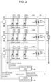
- FIG. 2 shows an electric circuit of a pulse power module 13 shown in FIG. 1 .
- FIG. 3 is a flowchart showing processing of a laser control unit 30 for controlling pulse energy of pulse laser light.
- FIG. 4 is a flowchart for describing a subroutine of drive timing setting processing in S 3 of FIG. 3 .
- FIG. 5 is a time chart for describing waveform control by setting the drive timing.
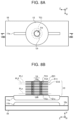
- FIG. 6 A is a plan view showing an example in which the pulse power module 13 is mounted on a circular substrate.
- FIG. 6 B schematically shows a cross-section along line VIB-A-VIB in FIG. 6 A .
- FIG. 7 schematically shows the structure of the pulse power module 13 configured by n primary electric circuits Eat to Ean and n transformer cores TC 1 to TCn.
- FIG. 8 A is a plan view showing a state in which the pulse power module 13 is arranged on a laser chamber 10 .
- FIG. 8 B is a sectional view along line VIIIB-VIIIB in FIG. 8 A .
- FIG. 9 A is a plan view showing a state in which the pulse power module 13 of a first embodiment of the present disclosure is arranged on the laser chamber 10 .
- FIG. 9 B is a sectional view along line IXB-IXB in FIG. 9 A .
- FIG. 10 is a plan view showing a state in which the pulse power module 13 of a second embodiment of the present disclosure is arranged on the laser chamber 10 .
- FIG. 11 is a plan view showing a state in which the pulse power module 13 of a third embodiment of the present disclosure is arranged on the laser chamber 10 .
- FIG. 12 shows a circuit diagram of the primary electric circuit Eai of the third embodiment.
- FIG. 13 is a plan view showing a state in which the pulse power module 13 of a fourth embodiment of the present disclosure is arranged on the laser chamber 10 .
- FIG. 14 is a plan view showing a state in which the pulse power module 13 of a fifth embodiment of the present disclosure is arranged on the laser chamber 10 .
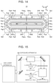
- FIG. 15 schematically shows the configuration of an exposure apparatus 100 connected to the gas laser apparatus 1 .
- FIG. 1 schematically shows the configuration of a gas laser apparatus 1 according to a comparative example.
- FIG. 1 shows the internal configuration of the gas laser apparatus 1 viewed from a direction substantially perpendicular to a discharge direction between a pair of discharge electrodes 11 a , 11 b and substantially perpendicular to the travel direction of laser light output from an output coupling mirror 15 .
- the travel direction of the laser light output from the output coupling mirror 15 is represented by the +Z direction.
- the discharge direction between the discharge electrodes 11 a , 11 b is represented by the +V direction or the ⁇ V direction.
- the direction perpendicular to the both is represented by the +H direction or the ⁇ H direction.
- the Z direction corresponds to the first direction in the present disclosure.
- the H direction corresponds to the second direction in the present disclosure.
- the ⁇ V direction substantially coincides with the direction of gravity.
- the gas laser apparatus 1 is used together with an exposure apparatus 100 .
- Laser light emitted from the gas laser apparatus 1 is incident on the exposure apparatus 100 .
- the exposure apparatus 100 includes an exposure apparatus control unit 110 .
- the exposure apparatus control unit 110 is configured to control the exposure apparatus 100 .
- the exposure apparatus control unit 110 is configured to transmit setting data and an oscillation trigger signal of target pulse energy Et to a laser control unit 30 included in the gas laser apparatus 1 .
- the gas laser apparatus 1 includes a laser chamber 10 , a charger 12 , a pulse power module 13 , a line narrowing module 14 , the output coupling mirror 15 , an energy monitor 17 , a crossflow fan 21 , a motor 22 , and the laser control unit 30 .
- the gas laser apparatus 1 is, for example, an excimer laser apparatus.
- the laser control unit 30 controls the entire gas laser apparatus 1 .
- the laser chamber 10 is arranged on an optical path of a laser resonator configured by the line narrowing module 14 and the output coupling mirror 15 .
- the laser chamber 10 is provided with two windows 10 a , 10 b .
- the laser chamber 10 accommodates the discharge electrodes 11 a , 11 b .
- the laser chamber 10 contains laser gas as a laser medium.
- the laser gas includes, for example, argon gas, fluorine gas, and neon gas.
- the laser gas includes, for example, krypton gas, fluorine gas, and neon gas.
- An opening is formed in a part of the laser chamber 10 , which is closed by an electrically insulating portion 29 .
- the electrically insulating portion 29 supports the discharge electrode 11 a .
- a plurality of conductive portions 29 a are embedded in the electrically insulating portion 29 . Each of the conductive portions 29 a is electrically connected to the discharge electrode 11 a.
- a return plate 10 c is arranged in the laser chamber 10 .
- a conductive member of the laser chamber 10 is electrically connected to the return plate 10 c .
- the return plate 10 c supports the discharge electrode 11 b .
- the return plate 10 c is electrically connected to the discharge electrode 11 b .
- gaps (not shown) through which the laser gas passes are provided on the front and back sides of the sheet of FIG. 1 .
- the crossflow fan 21 is arranged in the laser chamber 10 .
- a rotation axis of the crossflow fan 21 is connected to the motor 22 arranged outside the laser chamber 10 .
- the motor 22 rotates the crossflow fan 21 .
- the laser gas circulates in the laser chamber 10 .
- the charger 12 holds electric energy to be supplied to the pulse power module 13 .
- the pulse power module 13 includes a switch SW.
- the charger 12 is connected to the pulse power module 13 .
- the pulse power module 13 is connected to the discharge electrode 11 a through the conductive portions 29 a.
- the line narrowing module 14 includes wavelength selection elements such as a prism 14 a and a grating 14 b . Instead of the line narrowing module 14 , a high reflection mirror may be used.
- the output coupling mirror 15 is configured by a partial reflection mirror.
- the energy monitor 17 includes a beam splitter 17 a , alight concentrating lens 17 b , and a light sensor 17 c .
- the beam splitter 17 a is arranged in the optical path of the laser light output from the output coupling mirror 15 .
- the beam splitter 17 a is configured to transmit a part of the laser light output from the output coupling mirror 15 toward the exposure apparatus 100 at high transmittance and to reflect the other part.
- the light concentrating lens 17 b and the light sensor 17 c are arranged in the optical path of the laser light reflected by the beam splitter 17 a.
- the laser control unit 30 receives the setting data of the target pulse energy Et and the oscillation trigger signal from the exposure apparatus control unit 110 .
- the laser control unit 30 transmits a setting signal of a charge voltage to the charger 12 based on the setting data of the target pulse energy Et received from the exposure apparatus control unit 110 . Further, the laser control unit 30 transmits the oscillation trigger signal received from the exposure apparatus control unit 110 to the pulse power module 13 .
- the pulse power module 13 When the pulse power module 13 receives the oscillation trigger signal from the laser control unit 30 , the pulse power module 13 generates a pulse high voltage from the electric energy charged in the charger 12 and applies the high voltage between the discharge electrodes 11 a , 11 b.
- the light generated in the laser chamber 10 is emitted to the outside of the laser chamber 10 through the windows 10 a , 10 b .
- the beam width of the light emitted through the window 10 a of the laser chamber 10 is expanded by the prism 14 a , and then the light is incident on the grating 14 b .
- the light incident on the grating 14 b from the prism 14 a is reflected by a plurality of grooves of the grating 14 b and is diffracted in a direction corresponding to a wavelength of the light.
- the grating 14 b is disposed in the Littrow arrangement, which causes the incident angle of the light incident on the grating 14 b from the prism 14 a to coincide with the diffraction angle of the diffracted light having a desired wavelength.
- light having a wavelength close to the desired wavelength returns into the laser chamber 10 via the prism 14 a.
- the output coupling mirror 15 transmits and outputs apart of the light emitted from the window 10 b of the laser chamber 10 , and reflects the other part back into the laser chamber 10 .
- the light emitted from the laser chamber 10 reciprocates between the line narrowing module 14 and the output coupling mirror 15 .
- This light is amplified every time it passes through a discharge space between the discharge electrodes 11 a , 11 b . Further, this light is line narrowed each time it is turned back in the line narrowing module 14 .
- the light having undergone laser oscillation and line narrowing is output as laser light from the output coupling mirror 15 .
- the light concentrating lens 17 b included in the energy monitor 17 concentrates the laser light reflected by the beam splitter 17 a on the light sensor 17 c .
- the light sensor 17 c transmits an electric signal corresponding to pulse energy of the laser light concentrated by the light concentrating lens 17 b to the laser control unit 30 as measurement data.
- the laser control unit 30 receives the measurement data from the energy monitor 17 .
- the laser control unit 30 performs feedback control of the charge voltage set to the charger 12 based on the measurement data of the pulse energy received from the energy monitor 17 and the setting data of the target pulse energy Et received from the exposure apparatus control unit 110 .
- FIG. 2 shows an electric circuit of the pulse power module 13 shown in FIG. 1
- the pulse power module 13 of the comparative example includes n primary electric circuits Ea 1 to Ean, a secondary electric circuit Eb, and a circuit drive unit 60 .
- the pulse power module 13 is a pulse compression circuit configured by a linear transformer driver (LTD).
- the pulse power module 13 is connected to the laser control unit 30 through a signal line.
- the charger 12 described with reference to FIG. 1 is configured by n chargers 121 to 12 n as shown in FIG. 2 .
- the n chargers 121 to 12 n are connected to the n primary electric circuits Ea 1 to Ean, respectively.
- n is a natural number equal to or more than 2 and is, for example, a natural number in the range of 15 to 30.
- Each charger 12 i of the n chargers 121 to 12 n is a DC power supply device.
- i is an arbitrary natural number equal to or more than 1 and equal to or less than n.
- n components X 1 to Xn may be distinguished from each other by assigning numbers 1 to n to the reference signs of n components X.
- the reference sign Xi may substitute for referring to one of the n components X 1 to Xn.
- the reference sign Yi When one of n components Y 1 to Yn different from the n components X 1 to Xn is substituted by the reference sign Yi, it is indicated that the component Xi and the component Yi have a correspondence relationship therebetween.
- Each primary electric circuit Eai of the n primary electric circuits Ea 1 to Ean has one terminal connected to a reference potential and the other terminal connected to the charger 12 i . That is, the n primary electric circuits Ea 1 to Ean are connected in parallel to each other.
- the reference potential is, for example, a ground potential.
- the n chargers 121 to 12 n are connected to the laser control unit 30 through signal lines.
- the primary electric circuit Eai includes a primary coil Lai and m pulse generation units Pi 1 to Pim. That is, the n primary electric circuits Ea 1 to Ean include n primary coils La 1 to Lan and n ⁇ m pulse generation units each indicated by the reference sign Pij.
- m is a natural number equal to or more than 2 and is, for example, a natural number in the range of 15 to 30.
- j is an arbitrary natural number equal to or more than 1 and equal to or less than m.
- m components X 1 to Xm may be distinguished from each other by assigning numbers 1 to m to the reference signs of m components X.
- the reference sign Xj may substitute for referring to one of the m components X 1 to Xm.
- n ⁇ m components X 11 to Xnm may be distinguished from each other by assigning numbers 11 to nm to the reference signs of n ⁇ m components X.
- the reference sign Xij may substitute for referring to one of the n ⁇ m components X 11 to Xnm.
- the pulse generation unit Pij includes a capacitor Cij and a switch SWij.
- the capacitor Cij and the switch SWij are connected in series.
- m pulse generation units Pi 1 to Pim are connected in parallel to each other. Further, the primary coil Lai is connected in parallel to the m pulse generation units Pi 1 to Pim. Among the terminals at both ends of the primary coil Lai, one terminal is connected to the reference potential and the other terminal is connected to an output terminal of the charger 12 i . Among the terminals at both ends of the pulse generation unit Pij, the terminal located on the switch SWij side is connected to the reference potential and the terminal located on the capacitor Cij side is connected to the output terminal of the charger 12 i.
- the switch SWij is configured by, for example, a metal-oxide-semiconductor field-effect transistor (MOSFET).
- MOSFET metal-oxide-semiconductor field-effect transistor
- a drain terminal of the MOSFET configuring the switch SWij is connected to one terminal of the capacitor Cij.
- a source terminal of the MOSFET is connected to the reference potential.
- a gate terminal of the MOSFET is connected to the circuit drive unit 60 through a signal line.
- n signal lines are connected to the circuit drive unit 60 .
- the n signal lines are connected to the n primary electric circuits Ea 1 to Ean, respectively.
- Each of the n signal lines branches into m signal lines.
- the m signal lines are connected to m switches Swi 1 to SWim included in the primary electric circuit Eai, respectively. That is, the m signal lines are connected to m gate terminals of the m MOSFETs, respectively.
- One terminal of the secondary electric circuit Eb is connected to the discharge electrode 11 a .
- the other terminal of the secondary electric circuit Eb and the discharge electrode 11 b are both connected to the reference potential.
- the secondary electric circuit Eb includes n secondary coils Lb 1 to Lbn and n diodes Db 1 to Dbn.
- the n secondary coils Lb 1 to Lbn are connected in series to each other.
- the n diodes Db 1 to Dbn are connected in parallel to the n secondary coils Lb 1 to Lbn, respectively.
- a transformer is configured of the n primary coils La 1 to Lan, the n secondary coils Lb 1 to Lbn, and n transformer cores TC 1 to TCn (see FIG. 6 A to FIG. 9 B ).
- the n transformer cores TC 1 to TCn and each transformer core TCi will be described later.
- the laser control unit 30 transmits a setting signal of the charge voltage to then chargers 121 to 12 n .
- a charge voltage ⁇ V set to each of the n chargers 121 to 12 n is, for example, substantially the same value.
- the charge voltage ⁇ V is, for example, a voltage having a positive potential with respect to the reference potential.
- the charge voltage ⁇ V may be, for example, about 1 kV.
- Each charger 12 i of the n chargers 121 to 12 n charges the m capacitors Ci 1 to Cim included in the primary electric circuit Eai with the charge voltage ⁇ V.
- the laser control unit 30 outputs timing data and the oscillation trigger signal to the circuit drive unit 60 .
- the timing data defines drive timing of each of the n primary electric circuits Ea 1 to Ean.
- the timing data may include information defining, among the n primary electric circuits Ea 1 to Ean, which primary electric circuit is to be driven and which primary electric circuit is not to be driven.
- the number of the primary electric circuits to be driven among the n primary electric circuits Ea 1 to Ean and the breakdown thereof may be determined based on the target pulse energy Et of pulse laser light to be emitted from the gas laser apparatus 1 .
- the circuit drive unit 60 transmits a circuit drive signal to the primary electric circuit Eai based on the timing data and the oscillation trigger signal.
- the circuit drive signal is input substantially simultaneously to the m switches SWi 1 to SWim included in the primary electric circuit Eai.
- the m switches SWi 1 to SWim are switched from an off state to an on state substantially simultaneously, pulse currents flow substantially simultaneously from the m capacitors Ci 1 to Cim.
- the pulse current flowing from the m capacitors Ci 1 to Cim flows into the primary coil Lai. In the primary coil Lai, the pulse current flows downward from the upper side of FIG. 2 .
- the pulse current flowing through the primary coil Lai generates a magnetic flux at the transformer core TCi described later, and the generation of the magnetic flux generates an induced electromotive force at the secondary coil Lbi.
- a pulse voltage is applied between the pair of discharge electrodes 11 a , 11 b .
- the induced electromotive force generated at the secondary coil Lbi is substantially equal to the charge voltage ⁇ V of the charger 12 i .
- the number of the primary electric circuits that are driven simultaneously among the n primary electric circuits Ea 1 to Ean is large, the number of the secondary coils in which the induced electromotive force is generated simultaneously among the n secondary coils Lb 1 to Lbn becomes large. For example, when the number of the primary electric circuits that are driven simultaneously among the n primary electric circuits Ea 1 to Ean is i, the voltage applied between the pair of discharge electrodes 11 a , 11 b is i ⁇ V.
- the induced electromotive force is generated simultaneously at the n ⁇ 1 secondary coils Lb 2 to Lbn.
- the diode Db 1 is not arranged, a large pulse current also flows in the remaining secondary coil Lb 1 connected in series to the n ⁇ 1 secondary coils Lb 2 to Lbn.
- the pulse current flowing in the secondary coil Lb 1 generates a magnetic flux at the transformer core TC 1 described later, and the generation of the magnetic flux generates an induced electromotive force at the primary coil La 1 .
- a voltage is applied to the m switches SW 11 to SW 1 m in the off state included in the primary electric circuit Ea 1 , which may damage these switches SW 11 to SWim.
- a voltage is also applied to the charger 121 by the induced electromotive force generated at the primary coil La 1 , which may damage the charger 121 .
- the diode Db 1 is arranged to suppress damage to the switches SW 11 to SWim and the charger 121 . That is, even when an induced electromotive force is generated at any of the n ⁇ 1 secondary coils Lb 2 to Lbn, the current flows in the diode Db 1 , so that the current is suppressed from flowing in the secondary coil Lb 1 .
- FIG. 3 is a flowchart showing processing of the laser control unit 30 for controlling the pulse energy of the pulse laser light.
- the laser control unit 30 sets application voltages V(T 1 ), V(T 2 ), V(T 3 ) to be applied between the pair of discharge electrodes 11 a , 11 b as follows.
- the application voltages V(T 1 ), V(T 2 ), V(T 3 ) are to be applied between the pair of discharge electrodes 11 a , 11 b at timing delayed from the oscillation trigger signal by times T 1 , T 2 , T 3 , respectively.
- V 0 (T 1 ), V 0 (T 2 ), and V 0 (T 3 ) are initial values of the application voltages V(T 1 ), V(T 2 ), V(T 3 ), respectively.
- T 1 to T 3 have the following relationship. T 1 ⁇ T 2 ⁇ T 3
- the time T 3 is a time within which the discharge necessary for emitting the pulse laser light having desired pulse energy can be continued.
- the application voltage V(T 1 ) has the maximum absolute value.
- the application voltage V(T 1 ) is set to a voltage at which at least the laser gas between the pair of discharge electrodes 11 a , 11 b causes dielectric breakdown to occur and main discharge can be started.
- the application voltages V(T 2 ), V(T 3 ) are each set to a voltage at which the main discharge started by the application voltage V(T 1 ) can be continued.
- the laser control unit 30 reads the target pulse energy Et set by the exposure apparatus control unit 110 .
- the laser control unit 30 performs drive timing setting processing.
- the drive timing setting processing is processing of creating timing data by setting the drive timing of each of the n primary electric circuits Ea 1 to Ean. Details of the drive timing setting processing will be described later with reference to FIG. 4 .
- the laser control unit 30 outputs the timing data created in S 3 to the circuit drive unit 60 .
- the laser control unit 30 outputs the oscillation trigger signal received from the exposure apparatus control unit 110 to the circuit drive unit 60 .
- the circuit drive unit 60 controls driving of the n primary electric circuits Ea 1 to Ean based on the timing data and the oscillation trigger signal. Specifically, the circuit drive unit 60 may drive the primary electric circuits to be driven among the n primary electric circuits Ea 1 to Ean at the timing delayed by the times T 1 , T 2 , T 3 respectively from the oscillation trigger signal.
- the number of the primary electric circuits to be driven among the n primary electric circuits Ea 1 to Ean and breakdown thereof will be described later with reference to FIG. 4 .
- the laser control unit 30 determines whether laser oscillation is performed. When laser oscillation is performed, the laser control unit 30 waits until laser oscillation is performed. When laser oscillation is performed, the laser control unit 30 proceeds to S 7 .
- the laser control unit 30 obtains a measurement value E of the pulse energy measured by the energy monitor 17 .
- the laser control unit 30 calculates a difference ⁇ E between the measurement value E of the pulse energy and the target pulse energy Et.
- the laser control unit 30 sets new application voltages V(T 1 ), V(T 2 ), V(T 3 ) so that the difference ⁇ E approaches 0.
- the new application voltages V(T 1 ), V(T 2 ), V(T 3 ) are set using the following equations.
- V ( T 1) V ( T 1)+ ⁇ 1 ⁇ E
- V ( T 2) V ( T 2)+ ⁇ 2 ⁇ E
- V ( T 3) V ( T 3)+ ⁇ 3 ⁇ E
- ⁇ 1 , ⁇ 2 , and ⁇ 3 on the right sides may be proportional constants obtained in advance by experiments or the like.
- the laser control unit 30 determines whether the target pulse energy Et is changed.
- the exposure apparatus control unit 110 may change the target pulse energy Et.
- the exposure apparatus control unit 110 outputs setting data of the changed target pulse energy Et to the laser control unit 30 .
- the laser control unit 30 determines whether to end the processing of controlling the pulse energy of the pulse laser light. When the processing of controlling the pulse energy of the pulse laser light is not to be ended (S 11 : NO), the laser control unit 30 returns to S 3 . When the processing of controlling the pulse energy of the pulse laser light is to be ended (S 11 : YES), the laser control unit 30 ends the processing of the present flowchart.
- FIG. 4 is a flowchart for describing a subroutine of the drive timing setting processing in S 3 of FIG. 3 .
- the laser control unit 30 sets an identification number i to 1.
- the identification number i when the identification number i is set, one primary electric circuit Eai among the n primary electric circuits Ea 1 to Ean is identified.
- the identification number i when the identification number i is set, one charger 12 i corresponding to the primary electric circuit Eai is also identified.
- the laser control unit 30 sets the drive timing of the primary electric circuit Eai while counting up the identification number i.
- the laser control unit 30 determines whether the total value of the charge voltages of the i chargers 121 to 12 i identified by the identification numbers 1 to i is equal to or smaller than the application voltage V(T 1 ).
- the application voltage V(T 1 ) is the value set in S 1 of FIG. 3 as the application voltage to be applied between the pair of discharge electrodes 11 a , 11 b at the time T 1 .
- the total value of the charge voltages of the i chargers 121 to 12 i is expressed by i ⁇ V. Therefore, the determination in S 302 is performed based on whether the following condition is satisfied. i ⁇ V ⁇ V ( T 1)
- the laser control unit 30 proceeds to S 305 .
- the laser control unit 30 proceeds to S 303 .
- the laser control unit 30 sets the drive timing of the primary electric circuit Eai identified by the identification number i to the time T 1 .
- the laser control unit 30 updates the value of the identification number i by adding 1 to the value of the identification number i. Thereafter, the laser control unit 30 returns to S 302 .
- the laser control unit 30 sets a first threshold value k 1 to the current identification number i.
- the k 1 ⁇ 1 primary electric circuits Ea 1 to Eak 1 ⁇ 1 identified by the identification numbers 1 to k 1 ⁇ 1 less than the first threshold value k 1 are the primary electric circuits to be driven at the timing delayed by the time T 1 from the oscillation trigger signal.
- the primary electric circuits Eak 1 to Ean identified by the identification numbers k 1 to n equal to or more than the first threshold value k 1 are the primary electric circuits not to be driven at the timing delayed by the time T 1 from the oscillation trigger signal.
- the laser control unit 30 determines whether the total value of the charge voltages of the i-k 1 +1 chargers 12 k 1 to 12 i identified by the identification numbers k 1 to i is equal to or smaller than the application voltage V(T 2 ).
- the application voltage V(T 2 ) is the value set in S 1 of FIG. 3 as the application voltage to be applied between the pair of discharge electrodes 11 a , 11 b at the time T 2 .
- the total value of the charge voltages of the i ⁇ k 1 +1 chargers 12 k 1 to 12 i is expressed by (i ⁇ k 1 +1) ⁇ V. Therefore, the determination in S 306 is performed based on whether the following condition is satisfied. ( i ⁇ k 1 +1) ⁇ V ⁇ V ( T 2)
- the laser control unit 30 proceeds to S 309 .
- the laser control unit 30 proceeds to S 307 .
- the laser control unit 30 sets the drive timing of the primary electric circuit Eai identified by the identification number i to the time T 2 .
- the laser control unit 30 updates the value of the identification number i by adding 1 to the value of the identification number i. Thereafter, the laser control unit 30 returns to S 306 .
- the laser control unit 30 sets a second threshold value k 2 to the current identification number i.
- the k 2 ⁇ k 1 primary electric circuits Eak 1 to Eak 2 ⁇ 1 identified by the identification numbers k 1 to k 2 ⁇ 1 equal to or more than the first threshold value k 1 and less than the second threshold value k 2 are the primary electric circuits to be driven at the timing delayed by the time T 2 from the oscillation trigger signal.
- the primary electric circuits Ea 1 to Eak 1 ⁇ 1 and Eak 2 to Ean identified by the identification numbers 1 to k 1 ⁇ 1 and k 2 to n are the primary electric circuits not to be driven at the timing delayed by the time T 2 from the oscillation trigger signal.
- the laser control unit 30 determines whether the total value of the charge voltages of the i ⁇ k 2 +1 chargers 12 k 2 to 12 i identified by the identification numbers k 2 to i is equal to or smaller than the application voltage V(T 3 ).
- the application voltage V(T 3 ) is the value set in S 1 of FIG. 3 as the application voltage to be applied between the pair of discharge electrodes 11 a , 11 b at the time T 3 .
- the total value of the charge voltages of the i ⁇ k 2 +1 chargers 12 k 2 to 12 i is expressed by (i ⁇ k 2 +1) ⁇ V. Therefore, the determination in S 310 is performed based on whether the following condition is satisfied. ( i ⁇ k 2 +1) ⁇ V ⁇ V ( T 3)
- the laser control unit 30 proceeds to S 313 .
- the laser control unit 30 proceeds to S 311 .
- the laser control unit 30 sets the drive timing of the primary electric circuit Eai identified by the identification number i to the time T 3 .
- the laser control unit 30 updates the value of the identification number i by adding 1 to the value of the identification number i. Thereafter, the laser control unit 30 returns to S 310 .
- the laser control unit 30 sets a third threshold value k 3 to the current identification number i.
- the k 3 ⁇ k 2 primary electric circuits Eak 2 to Eak 3 ⁇ 1 identified by the identification numbers k 2 to k 3 ⁇ 1 equal to or more than the second threshold value k 2 and less than the third threshold value k 3 are the primary electric circuits to be driven at the timing delayed by the time T 3 from the oscillation trigger signal.
- the primary electric circuits Ea 1 to Eak 2 ⁇ 1 and Eak 3 to Ean identified by the identification numbers 1 to k 2 ⁇ 1 and k 3 to n are the primary electric circuits not to be driven at the timing delayed by the time T 3 from the oscillation trigger signal.
- the laser control unit 30 sets the switches SWi 1 to SWim included in the primary electric circuit Eai having the identification number i to the off state. That is, the primary electric circuit Eai having the identification number i is set as the primary electric circuit not to be driven.
- the laser control unit 30 updates the value of the identification number i by adding 1 to the value of the identification number i.
- the laser control unit 30 determines whether the value of the current identification number i is more than the number n of the primary electric circuits Ea 1 to Ean. When the value of the current identification number i is equal to or less than the number n of the primary electric circuits Ea 1 to Ean (S 316 : NO), the laser control unit 30 returns to S 314 . When the value of the current identification number i is more than the number n of the primary electric circuits Ea 1 to Ean (S 316 : YES), the laser control unit 30 ends the processing of the present flowchart and proceeds to S 4 of FIG. 3 .
- the timing data is generated as described above.
- FIG. 5 is a time chart for describing waveform control by setting the drive timing.
- the horizontal axis of FIG. 5 shows time T.
- the vertical axis of FIG. 5 shows intensity of signals such as a voltage V.
- the laser control unit 30 outputs the oscillation trigger signal to the circuit drive unit 60 . In addition to the oscillation trigger signal, the laser control unit 30 outputs the timing data to the circuit drive unit 60 .
- the circuit drive unit 60 transmits a circuit drive signal to the primary electric circuits Ea 1 to Eak 1 ⁇ 1 identified by the identification numbers 1 to k 1 ⁇ 1 at the timing delayed by the time T 1 from the oscillation trigger signal.
- the switches SWij included in the primary electric circuits Ea 1 to Eak 1 ⁇ 1 are switched to the on state.
- the circuit drive unit 60 transmits the circuit drive signal to the primary electric circuits Eak 1 to Eak 2 ⁇ 1 identified by the identification numbers k 1 to k 2 ⁇ 1 at the timing delayed by the time T 2 from the oscillation trigger signal.
- the switches SWij included in the primary electric circuits Eak 1 to Eak 2 ⁇ 1 are switched to the on state.
- the circuit drive unit 60 transmits the circuit drive signal to the primary electric circuits Eak 2 to Eak 3 ⁇ 1 identified by the identification numbers k 2 to k 3 ⁇ 1 at the timing delayed by the time T 3 from the oscillation trigger signal.
- the switches SWij included in the primary electric circuits Eak 2 to Eak 3 -1 are switched to the on state.
- the circuit drive unit 60 maintains the switches SWij included in the primary electric circuits Eak 3 to Ean identified by the identification numbers k 3 to n in the off state.
- each primary electric circuit Eai of the primary electric circuits Ea 1 to Eak 3 -1 when the switches SWij are switched to the on state, a pulse voltage having a peak value being the charge voltage ⁇ V is applied to both ends of the primary coil Lai.
- Each primary electric circuit Eai of the primary electric circuits Eak 3 to Ean is maintained in a non-driven state.
- a voltage Vs (T 1 ) due to induced electromotive forces is generated at the timing delayed by the time T 1 from the oscillation trigger signal.
- the voltage Vs (T 1 ) corresponds to the voltage obtained by summing the voltages applied to the primary coils La 1 to Lak 1 ⁇ 1 in the k 1 ⁇ 1 primary electric circuits Ea 1 to Eak 1 ⁇ 1.
- the peak value of the voltage Vs (T 1 ) is (k 1 ⁇ 1) ⁇ V.
- a voltage Vs(T 2 ) due to induced electromotive forces is generated at the timing delayed by the time T 2 from the oscillation trigger signal.
- the voltage Vs(T 2 ) corresponds to the voltage obtained by summing the voltages applied to the primary coils Lak 1 to Lak 2 ⁇ 1 in the k 2 ⁇ k 1 primary electric circuits Eak 1 to Eak 2 ⁇ 1.
- the peak value of the voltage Vs (T 2 ) is (k 2 ⁇ k 1 ) ⁇ V.
- a voltage Vs(T 3 ) due to induced electromotive forces is generated at the timing delayed by the time T 3 from the oscillation trigger signal.
- the voltage Vs(T 3 ) corresponds to the voltage obtained by summing the voltages applied to the primary coils Lake to Lak 3 ⁇ 1 in the k 3 ⁇ k 2 primary electric circuits Eak 2 to Eak 3 ⁇ 1.
- the peak value of the voltage Vs (T 3 ) is (k 3 ⁇ k 2 ) ⁇ V.
- the number k 1 ⁇ 1 of the primary electric circuits Ea 1 to Eak 1 ⁇ 1 driven at the timing of the time T 1 is preferably more than the number k 2 ⁇ k 1 of the primary electric circuits Eak 1 to Eak 2 ⁇ 1 driven at the timing of the time T 2 .
- the number k 1 ⁇ 1 of the primary electric circuits Ea 1 to Eak 1 ⁇ 1 driven at the timing of the time T 1 is preferably more than the number k 3 ⁇ k 2 of the primary electric circuits Eak 1 to Eak 3 ⁇ 1 driven at the timing of the time T 3 .
- the absolute value of the peak value of the voltage Vs (T 1 ) generated at the k 1 ⁇ 1 secondary coils Lb 1 to Lbk 1 ⁇ 1 is more than the absolute value of the peak value of the voltage Vs(T 2 ) generated at the k 2 ⁇ k 1 secondary coils Lbk 1 to Lbk 2 ⁇ 1.
- the absolute value of the peak value of the voltage Vs(T 1 ) generated at the k 1 ⁇ 1 secondary coils Lb 1 to Lbk 1 ⁇ 1 is more than the absolute value of the peak value of the voltage Vs(T 3 ) generated at the k 3 ⁇ k 2 secondary coils Lbk 2 to Lbk 3 ⁇ 1.
- the pulse waveform of a voltage Vr applied between the pair of discharge electrodes 11 a , 11 b has a waveform substantially similar to the waveform of the voltage Vs(T 1 ) until immediately before dielectric breakdown occurs.
- the voltage Vr suddenly approaches 0.
- the voltages Vs(T 2 ), Vs(T 3 ) are applied, the voltage Vr does not become 0 and is maintained at a voltage at which the main discharge can be continued.
- the laser gas is excited by the main discharge to emit light, and pulse laser light is emitted from the gas laser apparatus 1 .
- the pulse waveform of the pulse laser light is substantially similar to the pulse waveform of the current flowing in the secondary electric circuit Eb.
- FIG. 6 A is a plan view showing an example in which the pulse power module 13 is mounted on a circular substrate.
- FIG. 6 B schematically shows a cross-section along line VIB-A-VIB in FIG. 6 A .
- the secondary coil Lb is shown in a side view rather than in a cross-section.
- FIGS. 6 A and 6 B show one primary electric circuit Eai among the n primary electric circuits Ea 1 to Ean, one transformer core TCi, and a part of the secondary coil Lb.
- the transformer core TCi has a ring shape. As shown in FIG. 6 A , a magnetic circuit MC is formed along the ring configuring the transformer core TCi. As shown in FIG. 6 B , the transformer core TCi is located on a first plane PLi. The first plane PLi is parallel to the HZ plane. The magnetic circuit MC is formed along the first plane PLi.
- the secondary coil Lb is formed of a conductive member having a cylindrical shape. As shown in FIG. 6 B , the secondary coil Lb has a through hole TH. The through hole TH passes through the secondary coil Lb in a direction perpendicular to the first plane PLi. Illustration of n diodes Db 1 to Dbn is omitted.
- the primary electric circuit Eai includes substrates E 1 i and E 2 i and components mounted on the substrate E 1 i .
- the substrate E 2 i is omitted.
- the substrates E 1 i and E 2 i are both parallel to the first plane PLi.
- the transformer core TCi is also mounted on the substrate E 1 i .
- the substrates E 1 i and E 2 i each include a conductive member.
- the substrates E 1 i and E 2 i are both connected to the reference potential.
- the components mounted on the substrate E 1 i include a plurality of primary coils Lai 1 and Lai 1 , m pulse generation units Pi 1 to Pim, m switch drive units DRi 1 to DRim, and a plurality of conductive members E 3 i and E 4 i .
- the components mounted on the substrate E 1 i are arranged between the substrates E 1 i and E 2 i together with the transformer core TCi.
- Each of the substrates E 1 i and E 2 i and the transformer core TCi has a through hole, and the secondary coil Lb penetrates the through holes in a direction perpendicular to the first plane PLi.
- the m pulse generation units Pi 1 to Pim and the m switch drive units DRi 1 to DRim are arranged radially around the transformer core TCi.
- the plurality of primary coils Lai 1 and Lai 2 each include a conductive member.
- the plurality of primary coils Lai 1 and Lai 2 are arranged in a space outside the secondary coil Lb and inside the transformer core TCi. That is, the plurality of primary coils Lai 1 and Lai 2 are arranged in a space between the secondary coil Lb and the transformer core TCi.
- one end of each of the primary coils Lai 1 and Lai 2 is electrically connected to the substrate E 2 i , and is connected to the reference potential through the substrate E 2 i.
- the m pulse generation units Pi 1 to Pim include m capacitors Ci 1 to Cim and m switches SWi 1 to SWim. As shown in FIG. 6 B , in each pulse generation unit Pij of the m pulse generation units Pi 1 to Pim, the capacitor Cij and the switch SWij are connected in series.
- the m switches SWi 1 to SWim are configured by m MOSFETs. Source terminals of the m MOSFETs configuring the m switches SWi 1 to SWim are electrically connected to the substrate E 1 i , and are connected to the reference potential through the substrate E 1 i . Gate terminals of the m MOSFETs configuring the m switches SWi 1 to SWim are connected to the m switch drive units DRi 1 to DRim through signal lines, respectively. Drain terminals of the m MOSFETs configuring the switches SWi 1 to SWim are electrically connected to terminals on one side of the m capacitors Ci 1 to Cim, respectively.
- the terminals on the other side of the m capacitors Ci 1 to Cim are electrically connected to ends of the plurality of primary coils Lai 1 and Lai 2 , respectively, opposite to the ends connected to the substrate E 1 i through the conductive members.
- the output terminal of the charger 12 (see FIG. 1 and FIG. 7 ) is electrically connected to the conductive members connecting the m capacitors Ci 1 to Cim and the plurality of primary coils Lai 1 and Lai 2 .
- the conductive members connecting the m capacitors Ci 1 to Cim and the plurality of primary coils Lai 1 and Lai 2 are arranged between the transformer core TCi and the substrate E 1 i .
- An electrically insulating member (not shown) is arranged between the substrate E 1 i and the conductive members connecting the m capacitors Ci 1 to Cim and the plurality of primary coils Lai 1 and Lai 2 .
- the plurality of conductive members E 3 i and E 4 i are electrically connected between the substrates E 1 i and E 2 i.
- FIGS. 6 A and 6 B the configuration of FIGS. 6 A and 6 B is similar to that described with reference to FIG. 2 .
- FIG. 7 schematically shows the structure of the pulse power module 13 configured by n primary electric circuits Eat to Ean and n transformer cores TC 1 to TCn.
- the n transformer cores TC 1 to TCn are arranged side by side in the V direction.
- the n transformer cores TC 1 to TCn are arranged such that each of the first planes PL 1 to PLn is parallel to the HZ plane.
- the secondary coil Lb is arranged so as to penetrate the through holes of the n transformer cores TC 1 to TCn.
- An upper end Lbu of the secondary coil Lb is connected to the reference potential, and a lower end Lbb of the secondary coil Lb is connected to the discharge electrode 11 a .
- the “coil” is not limited to a conductive wire having a plurality of turns. Even a conductive member only penetrating the through hole of the transformer core TCi corresponds to the coil of the present disclosure as long as magnetic energy can be transmitted between the conductive member and the transformer core TCi.
- the secondary coil Lb corresponds to that in which the n secondary coils Lb 1 to Lbn described with reference to FIG. 2 are connected in series.
- the n primary electric circuits Ea 1 to Ean are arranged side by side in the V direction.
- the plurality of primary coils Lai 1 and Lai 1 included in each of the primary electric circuit Eai of the n primary electric circuits Ea 1 to Ean are arranged in a space inside the transformer core TCi and outside the secondary coil Lb.
- the substrate E 11 included in the primary electric circuit Ea 1 may include a conductive member common with the substrate E 22 included in the primary electric circuit Eat adjacent to the primary electric circuit Ea 1 . That is, the substrate E 1 i included in the primary electric circuit Eai may include a conductive member common with the substrate E 2 i+ 1 included in the primary electric circuit Eai+1.
- i is a natural number in the range of 1 to n ⁇ 1.
- the substrate E 1 i itself may be commonly used as the substrate E 2 i+ 1, and the substrate E 2 i+ 1 may be omitted.
- the output terminal of the charger 12 is electrically connected to the conductive member connecting the m capacitors Ci 1 to Cim and each of the plurality of primary coils Lai 1 and Lai 1 .
- Each of resistance elements Ri 1 to Rim may be connected between the charger 12 and the primary electric circuit Eai.
- the charger 12 may be a common charger connected to the n primary electric circuits Ea 1 to Ean.
- FIG. 7 is similar to that described with reference to FIGS. 6 A and 6 B .
- the charger 12 charges the capacitors Cij included in the n primary electric circuits Ea 1 to Ean with the charge voltage ⁇ V.
- a pulse current flows from them capacitors C 11 to C 1 m .
- the pulse current flowing from the capacitors C 11 to C 1 m flows into the primary coils La 11 and La 12 .
- the pulse current flows upward from the lower side of FIG. 7 .
- the pulse current flowing in the primary coils La 11 and La 12 generates a magnetic flux at the transformer core TC 1 , and the generation of the magnetic flux generates an induced electromotive force at the secondary coil Lb.
- a pulse voltage is applied between the pair of discharge electrodes 11 a , 11 b .
- the induced electromotive force generated at the secondary coil Lb by driving one primary electric circuit Ea 1 is substantially equal to the charge voltage ⁇ V of the charger 12 .
- the voltage applied between the pair of discharge electrodes 11 a , 11 b is i ⁇ V.
- FIG. 8 A is a plan view showing a state in which the pulse power module 13 is arranged on the laser chamber 10 .
- FIG. 8 B is a sectional view along line VIIIB-VIIIB in FIG. 8 A .
- FIG. 8 B only the substrates E 21 and E 11 to E 1 n are shown for the n primary electric circuits Ea 1 to Ean, and other circuit elements are omitted.
- the n transformer cores TC 1 to TCn are arranged side by side in the V direction.
- the n transformer cores TC 1 to TCn are arranged such that each of the first planes PL 1 to PLn are parallel to the HZ plane.
- the secondary coil Lb is arranged so as to penetrate all through holes of the n transformer cores TC 1 to TCn.
- the upper end Lbu of the secondary coil Lb is connected to the reference potential, and the lower end Lbb of the secondary coil Lb is connected to the discharge electrode 11 a .
- the discharge electrode 11 b is connected to the reference potential.
- the substrate E 21 and the n substrates E 11 to E 1 n are arranged so as to sandwich the n transformer cores TC 1 to TCn.
- a pulse high voltage generated by the pulse power module 13 is applied to the vicinity of the center of the discharge electrode 11 a in the longitudinal direction.
- the inductance from the pulse power module 13 to each portion of the discharge electrode 11 a depends on the distance from the vicinity of the center of the discharge electrode 11 a in the longitudinal direction. Since the discharge electrode 11 a has an elongated shape, there is a case where the inductance from the pulse power module 13 to an end of the discharge electrode 11 a in the longitudinal direction is increased. Therefore, the current density in the discharge space between the pair of discharge electrodes 11 a , 11 b at the time of discharge in the discharge space may vary depending on the distance from the vicinity of the center of the discharge electrode 11 a in the longitudinal direction.
- the shape of the n transformer cores TC 1 to TCn is elongated in the longitudinal direction of the pair of discharge electrodes 11 a , 11 b . Accordingly, deviation of the inductance from the pulse power module 13 to each portion of the discharge electrode 11 a is reduced, and deviation of the current density can be reduced.
- FIG. 9 A is a plan view showing a state in which the pulse power module 13 of a first embodiment of the present disclosure is arranged on the laser chamber 10 .
- FIG. 9 B is a sectional view along line IXB-IXB in FIG. 9 A .
- the pulse power module 13 corresponds to the high voltage pulse generation device of the present disclosure.
- the laser chamber 10 has substantially the same shape as the substrates E 11 to E 1 n included in the pulse power module 13 in the plan view shown in FIG. 9 A . Therefore, only the pulse power module 13 is shown in FIG. 9 A . Since the n transformer cores TC 1 to TCn have the same configuration with each other and the n primary electric circuits Ea 1 to Ean have the same configuration with each other, the components X 1 to Xn are substituted by the reference sign Xi in FIG. 9 A . In FIG. 9 A , the substrate E 21 is omitted.
- each transformer core TCi of the n transformer cores TC 1 to TCn is a shape in which a width Wz in the Z direction is larger than a width Wh in the H direction.
- the Z direction is a first direction parallel to the first planes PL 1 to PLn.
- the H direction is a second direction parallel to the first planes PL 1 to PLn and perpendicular to the first direction.
- the transformer core TCi is arranged such that the Z direction, which is the longitudinal direction thereof, is parallel to the longitudinal direction of the pair of discharge electrodes 11 a , 11 b.
- the transformer core TCi includes first and second linear portions TCi 1 and TCi 2 and first and second curved portions TCi 3 and TCi 4 .
- the first and second linear portions TCi 1 and TCi 2 are arranged along the Z direction.
- the first curved portion TCi 3 connects ends of the first and second linear portions TCi 1 and TCi 2 on the +Z direction side.
- the second curved portion TCi 4 connects ends of the first and second linear portions TCi 1 and TCi 2 on the ⁇ Z direction side.
- the transformer core TCi has a racetrack shape.
- the shape of the transformer core TCi is not limited to the above shape and may be rectangular or elliptic.
- the width Wz of the transformer core TCi in the Z direction is preferably larger than the length DE (see FIG. 9 B ) in the longitudinal direction of the pair of discharge electrodes 11 a , 11 b .
- the width Wh of the transformer core TCi in the H direction is preferably larger than the length in the H direction of the pair of discharge electrodes 11 a , 11 b.
- the secondary coil Lb has a cylindrical shape having the through hole TH in a direction perpendicular to the first plane PLi, and having a width Wz 1 in the Z direction larger than a width Wh 1 in the H direction.
- the ratio of the Z direction width Wz 1 of the secondary coil Lb to the length DE in the longitudinal direction of the pair of discharge electrodes 11 a , 11 b is preferably equal to or more than 0.5 and equal to or less than 2.
- the ratio is more preferably equal to or more than 0.8 and equal to or less than 1.2. It is further preferable that the ratio is about 1.
- a gap GAP (see FIG. 9 B ) between the transformer core TCi and the secondary coil Lb is preferably equal to or smaller than 5 mm.
- the gap GAP is more preferably equal to or larger than 1 mm and equal to or smaller than 3 mm.
- the m pulse generation units include m 1 pulse generation units Pia 1 to Piam 1 and m 2 pulse generation units Pib 1 to Pibm 2 . These pulse generation units are arranged outside the magnetic circuit MC formed in the transformer core TCi.
- the m 1 pulse generation units Pia 1 to Piam 1 are arranged side by side in the Z direction on the ⁇ H direction side of the transformer core TCi.
- the m 2 pulse generation units Pib 1 to Pibm 2 are arranged side by side in the Z direction on the +H direction side of the transformer core TCi.
- the m 1 pulse generation units Pia 1 to Piam 1 and the m 2 pulse generation units Pib 1 to Pibm 2 are arranged on opposite sides of the transformer core TCi.
- the m switch drive units DRi 1 to DRim are omitted.
- Each of m 1 and m 2 is a natural number equal to or more than 2 and equal to or less than m.
- m 1 and m 2 may be different numbers, but are preferably the same number.
- the m 1 pulse generation units Pia 1 to Piam 1 have a first gap G 1 therebetween, and the m 2 pulse generation units Pib 1 to Pibm 2 have a second gap G 2 therebetween.
- the first gap G 1 and the second gap G 2 are substantially the same.
- the deviation of the inductance from the secondary coil Lb to each portion of the discharge electrode 11 a can be reduced. Accordingly, the deviation of the pulse current in the longitudinal direction of the discharge electrode 11 a can be reduced.
- the deviation of the pulse current in the longitudinal direction of the discharge electrode 11 a can be further reduced.
- the first gap G 1 between the m 1 pulse generation units Pia 1 to Piam 1 and the second gap G 2 between the m 2 pulse generation units Pib 1 to Pibm 2 substantially the same, the deviation of the pulse current in the longitudinal direction of the discharge electrode 11 a can be further reduced.
- the first embodiment is similar to the comparative example described above.
- FIG. 10 is a plan view showing a state in which the pulse power module 13 of a second embodiment of the present disclosure is arranged on the laser chamber 10 .
- the m pulse generation units further include m 3 ( 12 in FIG. 10 ) pulse generation units Pic 1 to Pic 12 in addition to the m 1 pulse generation units Pia 1 to Piam 1 and the m 2 pulse generation units Pib 1 to Pibm 2 .
- the m 3 pulse generation units Pic 1 to Pic 12 are arranged side by side around the first and second curved portions TCi 3 and TCi 4 .
- the direction in which the m 3 pulse generation units Pic 1 to Pic 12 are arranged is a direction different from the Z direction.
- the m 1 pulse generation units Pia 1 to Piam 1 have the first gap G 1 therebetween, and the m 2 pulse generation units Pib 1 to Pibm 2 have the second gap G 2 therebetween.
- Each of the first gap G 1 and the second gap G 2 may be smaller than a third gap G 3 between the m 3 pulse generation units Pic 1 to Pic 12 .
- m 3 is a natural number equal to or more than 2 and equal to or less than m. Further, m 3 may be the same number as m 1 or m 2 , or may be a different number.
- the current density in the discharge space in the vicinity of both ends of the pair of discharge electrodes 11 a , 11 b can be caused to be higher than that in the first embodiment.
- the current density in the discharge space in the vicinity of both ends of the pair of discharge electrodes 11 a , 11 b can be adjusted.
- m 3 small and the third gap G 3 larger than the first gap G 1 and the second gap G 2 it is possible to suppress the current density in the discharge space in the vicinity of both ends of the pair of discharge electrodes 11 a , 11 b from becoming too high.
- the second embodiment is similar to the first embodiment.
- FIG. 11 is a plan view showing a state in which the pulse power module 13 of a third embodiment of the present disclosure is arranged on the laser chamber 10 .
- the primary electric circuit Eai includes m 4 switch drive units DRi 1 to DRim 4 instead of the m switch drive units DRi 1 to DRim.
- the pulse generation units Pia 1 to Piam 1 , Pib 1 to Pibm 2 , and Pic 1 to Pic 12 included in the primary electric circuit Eai are divided into m 4 groups.
- Each of the m 4 groups includes a plurality of pulse generation units.
- the m 4 switch drive units DRi 1 to DRim 4 are configured to transmit a switch drive signal to the m 4 groups, respectively.
- the switch drive signal is input to the gate terminal of the MOSFET configuring the switch included in each of the pulse generation units Pia 1 to Piam 1 , Pib 1 to Pibm 2 , and Pic 1 to Pic 12 .
- m 4 is a natural number equal to or more than 2 and equal to or less than m and is, for example, 8.
- the primary electric circuit Eai further includes m 5 trigger input units TIi 1 to TIim 5 .
- the m 4 switch drive units DRi 1 to DRim 4 are divided into m 5 groups. Each of the m 5 groups includes a plurality of switch drive units.
- the m 5 trigger input units TIi 1 to TIim 5 are configured to provide a trigger signal to the m 5 groups, respectively.
- m 5 is a natural number equal to or more than 2 and equal to or less than m 4 and is, for example, 2.
- the signal lines connected respectively from the switch drive units DRi 1 , DRi 4 , DRi 5 , DRim 4 to the trigger input unit TIi 1 or TIim 5 are shorter than the signal lines connected respectively from the switch drive units DRi 2 , DRi 3 , DRi 6 , DRi 7 to the trigger input unit TIi 1 or TIim 5 . It is preferable that the m 4 switch drive units DRi 1 to DRim 4 are operated substantially simultaneously by causing delays according to the lengths of the signal lines.
- the gate resistances of the switching elements such as MOSFETs included in the switch drive units DRi 1 , DRi 4 , DRi 5 , DRim 4 may be set higher than those of the other switch drive units DRi 2 , DRi 3 , DRi 6 , DRi 7 .
- a delay circuit may be arranged in the middle of each of the signal lines connected respectively from the switch drive units DRi 1 , DRi 4 , DRi 5 , DRim 4 to the trigger input unit TIi 1 or TIim 5 .
- FIG. 12 shows a circuit diagram of the primary electric circuit Eai of the third embodiment.
- the circuit drive unit 60 is configured to output an optical signal as the circuit drive signal.
- the circuit drive unit 60 is connected to the m 5 trigger input units TIi 1 to TIim 5 through optical fibers.
- the optical signal output from the circuit drive unit 60 is input to the m 5 trigger input units TIi 1 to TIim 5 .
- Each of the m 5 trigger input units TIi 1 to TIim 5 is a converter that converts the optical signal into an electric signal. Signal lines of the electric signal output from the m 5 trigger input units TIi 1 to TIim 5 are each connected to any of the m 4 switch drive units DRi 1 to DRim 4 .
- the m 5 trigger input units TIi 1 to TIim 5 provide the electric signal to the m 4 switch drive units DRi 1 to DRim 4 as a trigger signal.
- Each of the m 4 switch drive units DRi 1 to DRim 4 receives an electric signal from any of the m 5 trigger input units TIi 1 to TIim 5 , and the switch drive signal is transmitted to the m pulse generation units Pi 1 to Pim.
- the m pulse generation units Pi 1 to Pim correspond to the pulse generation units Pia 1 to Piam 1 , Pib 1 to Pibm 2 , and Pic 1 to Pic 12 in FIG. 11 .
- the optical signal is input from the circuit drive unit 60 to the m 5 trigger input units TIi 1 to TIim 5 , it is possible to reduce a shift in operation timing between the m 5 trigger input units TIi 1 to TIim 5 .
- the lengths of the signal lines from the m 5 trigger input units TIi 1 to TIim 5 to the m 4 switch drive units DRi 1 to DRim 4 can be set smaller than the length DE of the pair of discharge electrodes 11 a , 11 b in the longitudinal direction.
- the lengths of the signal lines from the trigger input units TIi 1 to TIim 5 to the switch drive units DRi 1 to DRim 4 may be set smaller than half the length DE of the pair of discharge electrodes 11 a , 11 b in the longitudinal direction.
- the shift in the operation timing of the switch drive units DRi 1 to DRim 4 can be reduced.
- the switch drive signal can be transmitted from the m 4 switch drive units DRi 1 to DRim 4 to the pulse generation units Pia 1 to Piam 1 , Pib 1 to Pibm 2 , and Pic 1 to Pic 12 substantially simultaneously. Therefore, it is possible to reduce variations in the pulse generating timing among the pulse generation units Pia 1 to Piam 1 , Pib 1 to Pibm 2 , and Pic 1 to Pic 12 .
- the third embodiment is similar to the second embodiment.
- Pulse Power Module Including Many Trigger Input Units
- FIG. 13 is a plan view showing a state in which the pulse power module 13 of a fourth embodiment of the present disclosure is arranged on the laser chamber 10 .
- m 4 is 8 and m 5 is 2
- m 4 is 12 and m 5 is 6. That is, the pulse generation units Pia 1 to Piam 1 , Pib 1 to Pibm 2 , and Pic 1 to Pic 12 are divided into 12 groups, and the switch drive signal is transmitted from the 12 switch drive units DRi 1 to DRim 4 to the 12 groups, respectively.
- the 12 switch drive units DRi 1 to DRim 4 are divided into 6 groups, and the trigger signal is provided from the 6 trigger input units TIi 1 to TIim 5 to the 6 groups, respectively.
- the fourth embodiment is similar to the third embodiment.
- FIG. 14 is a plan view showing a state in which the pulse power module 13 of a fifth embodiment of the present disclosure is arranged on the laser chamber 10 .
- one primary electric circuit Eai and one transformer core TCi are mounted on first to fourth substrates Sb 1 to Sb 4 .
- m pulse generation units included in the primary electric circuit Eai includes m 6 pulse generation units Pid 1 to Pidm 1 mounted on the first substrate Sb 1 , and m 7 pulse generation units Pie 1 to Piem 7 mounted on the second substrate Sb 2 .
- the first substrate Sb 1 and the second substrate Sb 2 have substantially the same shape.
- m 6 and m 7 are the same number. Further, m 6 pulse generation units Pid 1 to Pidm 6 and m 7 pulse generation units Pie 1 to Piem 7 are mounted on the first substrate Sb 1 and the second substrate Sb 2 in the same arrangement, respectively. Thus, the manufacturing steps of the first substrate Sb 1 and the second substrate Sb 2 can be unified, and the manufacturing cost can be reduced. Further, the first substrate Sb 1 on which m 6 pulse generation units Pid 1 to Pidm 6 are mounted and the second substrate Sb 2 on which m 7 pulse generation units Pie 1 to Piem 7 are mounted can be made common as replacement parts.
- m pulse generation units included in the primary electric circuit Eai further include m 8 pulse generation units Pif 1 to Pifm 8 mounted on the third substrate Sb 3 , and m 9 pulse generation units Pig 1 to Pigm 9 mounted on the fourth substrate Sb 4 .
- the third substrate Sb 3 is substantially mirror symmetrical to the first substrate Sb 1 .
- the third substrate Sb 3 and the fourth substrate Sb 4 have substantially the same shape.
- m 8 and m 9 are the same number. Further, m 8 pulse generation units Pif 1 to Pifm 8 and m 9 pulse generation units Pig 1 to Pigm 9 are mounted on the third substrate Sb 3 and the fourth substrate Sb 4 in the same arrangement, respectively. Accordingly, it is possible to obtain the same effect as in the case of unifying the arrangement of the elements in the first substrate Sb 1 and the second substrate Sb 2 .
- the substrate on which the primary electric circuit Eai and the transformer core TCi are mounted is divided into 4 substrates Sb 1 to Sb 4 , but the present disclosure is not limited thereto.
- a similar effect can be obtained by dividing a substrate into 2 or more substrates having the same shape or mirror-symmetrical shapes.
- the fifth embodiment is similar to the third embodiment or the fourth embodiment.
- FIG. 15 schematically shows the configuration of the exposure apparatus 100 connected to the gas laser apparatus 1 .
- the gas laser apparatus 1 generates laser light and emits the laser light to the exposure apparatus 100 .
- the exposure apparatus 100 includes an illumination optical system 41 and a projection optical system 42 .
- the illumination optical system 41 illuminates a reticle pattern of a reticle stage RT with the laser light incident from the gas laser apparatus 1 .
- the projection optical system 42 causes the laser light transmitted through the reticle to be imaged as being reduced and projected on a workpiece (not shown) arranged on a workpiece table WT.
- the workpiece is a photosensitive substrate such as a semiconductor wafer on which photoresist is applied.
- the exposure apparatus 100 synchronously translates the reticle stage RT and the workpiece table WT to expose the workpiece to the laser light reflecting the reticle pattern. Through the exposure process as described above, a device pattern is transferred onto the semiconductor wafer, thereby an electronic device can be manufactured.
Landscapes
- Physics & Mathematics (AREA)
- Electromagnetism (AREA)
- Engineering & Computer Science (AREA)
- Plasma & Fusion (AREA)
- Optics & Photonics (AREA)
- Microelectronics & Electronic Packaging (AREA)
- Power Engineering (AREA)
- General Physics & Mathematics (AREA)
- Lasers (AREA)
Abstract
Description
- Patent Document 1: US Patent Application Publication No. 2017/0338618
- Patent Document 2: Japanese Patent Application Publication No. 2006-324039
-
- 1. Comparative example
- 1.1 Configuration of gas laser apparatus
- 1.2 Operation of gas laser apparatus
- 1.3 Configuration of pulse power module
- 1.3.1 Primary electric circuit
- 1.3.2 Secondary electric circuit
- 1.4 Operation of pulse power module
- 1.5 Operation of laser control unit
- 1.5.1 Main flow
- 1.5.2. Detail of drive timing setting processing
- 1.5.2.1 Primary electric circuit driven at time T1
- 1.5.2.2 Primary electric circuit driven at time T2
- 1.5.2.3 Primary electric circuit driven at time T3
- 1.5.2.4 Primary electric circuit not to be driven
- 1.5.3 Time chart
- 1.6 Arrangement on substrate
- 1.7 Structure in which n primary electric circuits are laminated
- 1.8 Problem
- 2. Pulse power module having transformer core elongated in Z direction
- 2.1 Configuration of transformer core
- 2.2 Configuration of secondary coil
- 2.3 Configuration of m pulse generation units
- 2.4 Effect
- 3. Pulse power module with increased number of pulse generation units
- 3.1 Configuration
- 3.2 Effect
- 4. Pulse power module including trigger input unit
- 4.1 Arrangement of elements
- 4.2 Circuit configuration
- 4.3 Effect
- 5. Pulse power module including many trigger input units
- 6. Pulse power module including divided substrate
- 7. Others
-
- V(T1)=V0 (T1)
- V(T2)=V0 (T2)
- V(T3)=V0 (T3)
T1<T2<T3
ΔE=E−Et
V(T1)=V(T1)+α1·ΔE
V(T2)=V(T2)+α2·ΔE
V(T3)=V(T3)+α3·ΔE
Here, α1, α2, and α3 on the right sides may be proportional constants obtained in advance by experiments or the like.
i·ΔV≤V(T1)
(i−k 1+1)·ΔV≤V(T2)
(i−k 2+1)·ΔV≤V(T3)
Claims (20)
Applications Claiming Priority (1)
| Application Number | Priority Date | Filing Date | Title |
|---|---|---|---|
| PCT/JP2019/012901 WO2020194515A1 (en) | 2019-03-26 | 2019-03-26 | High-voltage pulse generation device, gas laser device, and method for manufacturing electronic device |
Related Parent Applications (1)
| Application Number | Title | Priority Date | Filing Date |
|---|---|---|---|
| PCT/JP2019/012901 Continuation WO2020194515A1 (en) | 2019-03-26 | 2019-03-26 | High-voltage pulse generation device, gas laser device, and method for manufacturing electronic device |
Publications (2)
| Publication Number | Publication Date |
|---|---|
| US20210367393A1 US20210367393A1 (en) | 2021-11-25 |
| US12166329B2 true US12166329B2 (en) | 2024-12-10 |
Family
ID=72609669
Family Applications (1)
| Application Number | Title | Priority Date | Filing Date |
|---|---|---|---|
| US17/396,928 Active 2041-04-07 US12166329B2 (en) | 2019-03-26 | 2021-08-09 | High voltage pulse generation device, gas laser apparatus, and electronic device manufacturing method |
Country Status (3)
| Country | Link |
|---|---|
| US (1) | US12166329B2 (en) |
| CN (1) | CN113439371B (en) |
| WO (1) | WO2020194515A1 (en) |
Citations (13)
| Publication number | Priority date | Publication date | Assignee | Title |
|---|---|---|---|---|
| US4295103A (en) * | 1978-03-23 | 1981-10-13 | Ariold Ljudmirsky | Metal vapor laser |
| JP2001217492A (en) | 2000-02-01 | 2001-08-10 | Ushio Inc | Discharge excitation gas laser device |
| US20020186739A1 (en) * | 1999-09-27 | 2002-12-12 | Sandstrom Richard L. | Injection seeded F2 laser with wavelength control |
| JP2004064935A (en) | 2002-07-30 | 2004-02-26 | Ushio Inc | High-voltage pulse generator and discharge-excited gas laser using the same |
| US20050088855A1 (en) * | 2001-12-15 | 2005-04-28 | Thomas Kirchmeier | High frequency excitation system |
| JP2005347586A (en) | 2004-06-04 | 2005-12-15 | Ushio Inc | Winding device, high voltage pulse generation circuit using winding device, and discharge-excited gas laser apparatus provided with the high voltage pulse generation circuit |
| JP2006324039A (en) | 2005-05-17 | 2006-11-30 | Ushio Inc | Pulse generator and extreme ultraviolet light source device |
| US20150255948A1 (en) * | 2012-11-28 | 2015-09-10 | Par Systems (Pty) Ltd. | Laser excitation pulsing system |
| US20160190763A1 (en) * | 2013-10-02 | 2016-06-30 | Gigaphoton Inc. | Laser apparatus |
| WO2016152738A1 (en) | 2015-03-25 | 2016-09-29 | 国立大学法人長岡技術科学大学 | High-voltage pulse generating device and gas laser device |
| US20160359291A1 (en) * | 2014-03-18 | 2016-12-08 | Gigaphoton Inc. | Gas laser device and control method therefor |
| CN106532412A (en) | 2016-12-30 | 2017-03-22 | 华中科技大学 | Radio frequency exciting slab discharging two-dimensional voltage distribution model and voltage balancing method |
| US20210367394A1 (en) * | 2019-03-26 | 2021-11-25 | National University Corporation Nagaoka University Of Technology | High-voltage pulse generator, gas laser apparatus, and method for manufacturing electronic device |
Family Cites Families (6)
| Publication number | Priority date | Publication date | Assignee | Title |
|---|---|---|---|---|
| EP0261663B1 (en) * | 1986-09-26 | 1992-06-17 | Hitachi, Ltd. | Laser device with high-voltage pulse generator, high-voltage pulse generator and pulse generating method |
| JPS63229786A (en) * | 1987-03-19 | 1988-09-26 | Toshiba Corp | Power device for highly repetitive pulsed laser |
| JPH03261186A (en) * | 1990-03-09 | 1991-11-21 | Hitachi Ltd | pulse power supply |
| JP4171273B2 (en) * | 2002-09-30 | 2008-10-22 | ウシオ電機株式会社 | High voltage pulse generator and discharge excitation gas laser device using the same |
| WO2016084263A1 (en) * | 2014-11-28 | 2016-06-02 | ギガフォトン株式会社 | Narrowband laser device |
| CN109478757B (en) * | 2016-08-05 | 2021-04-16 | 极光先进雷射株式会社 | Gas laser device |
-
2019
- 2019-03-26 CN CN201980091052.5A patent/CN113439371B/en active Active
- 2019-03-26 WO PCT/JP2019/012901 patent/WO2020194515A1/en not_active Ceased
-
2021
- 2021-08-09 US US17/396,928 patent/US12166329B2/en active Active
Patent Citations (15)
| Publication number | Priority date | Publication date | Assignee | Title |
|---|---|---|---|---|
| US4295103A (en) * | 1978-03-23 | 1981-10-13 | Ariold Ljudmirsky | Metal vapor laser |
| US20020186739A1 (en) * | 1999-09-27 | 2002-12-12 | Sandstrom Richard L. | Injection seeded F2 laser with wavelength control |
| JP2001217492A (en) | 2000-02-01 | 2001-08-10 | Ushio Inc | Discharge excitation gas laser device |
| US20050088855A1 (en) * | 2001-12-15 | 2005-04-28 | Thomas Kirchmeier | High frequency excitation system |
| JP2004064935A (en) | 2002-07-30 | 2004-02-26 | Ushio Inc | High-voltage pulse generator and discharge-excited gas laser using the same |
| JP2005347586A (en) | 2004-06-04 | 2005-12-15 | Ushio Inc | Winding device, high voltage pulse generation circuit using winding device, and discharge-excited gas laser apparatus provided with the high voltage pulse generation circuit |
| JP2006324039A (en) | 2005-05-17 | 2006-11-30 | Ushio Inc | Pulse generator and extreme ultraviolet light source device |
| US20150255948A1 (en) * | 2012-11-28 | 2015-09-10 | Par Systems (Pty) Ltd. | Laser excitation pulsing system |
| JP2016506616A (en) | 2012-11-28 | 2016-03-03 | パー システムズ (ピーティーワイ) エルティーディー | Laser pumping pulse system |
| US20160190763A1 (en) * | 2013-10-02 | 2016-06-30 | Gigaphoton Inc. | Laser apparatus |
| US20160359291A1 (en) * | 2014-03-18 | 2016-12-08 | Gigaphoton Inc. | Gas laser device and control method therefor |
| WO2016152738A1 (en) | 2015-03-25 | 2016-09-29 | 国立大学法人長岡技術科学大学 | High-voltage pulse generating device and gas laser device |
| US20170338618A1 (en) * | 2015-03-25 | 2017-11-23 | National University Corporation Nagaoka University Of Technology | High-voltage pulse generator and gas laser apparatus |
| CN106532412A (en) | 2016-12-30 | 2017-03-22 | 华中科技大学 | Radio frequency exciting slab discharging two-dimensional voltage distribution model and voltage balancing method |
| US20210367394A1 (en) * | 2019-03-26 | 2021-11-25 | National University Corporation Nagaoka University Of Technology | High-voltage pulse generator, gas laser apparatus, and method for manufacturing electronic device |
Non-Patent Citations (2)
| Title |
|---|
| International Preliminary Report On Patentability and Written Opinion issued in PCT/JP2019/012901; issued Sep. 28, 2021. |
| International Search Report issued in PCT/JP2019/012901; mailed Jun. 25, 2019. |
Also Published As
| Publication number | Publication date |
|---|---|
| CN113439371A (en) | 2021-09-24 |
| CN113439371B (en) | 2023-12-08 |
| WO2020194515A1 (en) | 2020-10-01 |
| US20210367393A1 (en) | 2021-11-25 |
Similar Documents
| Publication | Publication Date | Title |
|---|---|---|
| JP6748993B2 (en) | High voltage pulse generator and gas laser device | |
| US9853410B2 (en) | Gas laser device and control method therefor | |
| US20210167568A1 (en) | Gas laser device | |
| US12166329B2 (en) | High voltage pulse generation device, gas laser apparatus, and electronic device manufacturing method | |
| CN109891689B (en) | Laser device | |
| US12244117B2 (en) | High-voltage pulse generator, gas laser apparatus, and method for manufacturing electronic device | |
| US20230268710A1 (en) | Gas laser apparatus and electronic device manufacturing method | |
| US9601893B2 (en) | Laser apparatus | |
| US6788008B2 (en) | Device for operating a dielectric barrier discharge lamp | |
| US6643312B2 (en) | ArF excimer laser device and a fluoride laser device | |
| JP2005185092A (en) | Apparatus for generating high repetition rate and high current intensity pulse-shaped current for gas discharge pumped radiation source | |
| JP2008171852A (en) | Gas discharge laser apparatus, exposure method and apparatus, and device manufacturing method | |
| US6636546B2 (en) | ArF and KrF excimer laser apparatus and fluorine laser apparatus for lithography | |
| US20240396284A1 (en) | Gas laser device and electronic device manufacturing method | |
| CN117441274A (en) | Electronic module for magnetic switching network for generating pulses of a pulsed output beam | |
| US20250364771A1 (en) | Gas laser apparatus and electronic device manufacturing method | |
| US20250364769A1 (en) | Laser chamber apparatus, gas laser apparatus, and electronic device manufacturing method | |
| US20240405501A1 (en) | Gas laser device and electronic device manufacturing method | |
| WO2024180767A1 (en) | Gas laser device, method for controlling temperature of laser gas, and method for manufacturing electronic device | |
| JP2004032912A (en) | High-voltage pulse generator and discharge exciting gas laser device using the same |
Legal Events
| Date | Code | Title | Description |
|---|---|---|---|
| AS | Assignment |
Owner name: NATIONAL UNIVERSITY CORPORATION NAGAOKA UNIVERSITY OF TECHNOLOGY, JAPAN Free format text: ASSIGNMENT OF ASSIGNORS INTEREST;ASSIGNORS:JIANG, WEIHUA;UMEDA, HIROSHI;KAKIZAKI, KOJI;SIGNING DATES FROM 20210601 TO 20210609;REEL/FRAME:057119/0100 Owner name: GIGAPHOTON INC., JAPAN Free format text: ASSIGNMENT OF ASSIGNORS INTEREST;ASSIGNORS:JIANG, WEIHUA;UMEDA, HIROSHI;KAKIZAKI, KOJI;SIGNING DATES FROM 20210601 TO 20210609;REEL/FRAME:057119/0100 |
|
| FEPP | Fee payment procedure |
Free format text: ENTITY STATUS SET TO UNDISCOUNTED (ORIGINAL EVENT CODE: BIG.); ENTITY STATUS OF PATENT OWNER: LARGE ENTITY |
|
| STPP | Information on status: patent application and granting procedure in general |
Free format text: DOCKETED NEW CASE - READY FOR EXAMINATION |
|
| STPP | Information on status: patent application and granting procedure in general |
Free format text: NON FINAL ACTION MAILED |
|
| STPP | Information on status: patent application and granting procedure in general |
Free format text: RESPONSE TO NON-FINAL OFFICE ACTION ENTERED AND FORWARDED TO EXAMINER |
|
| STPP | Information on status: patent application and granting procedure in general |
Free format text: NOTICE OF ALLOWANCE MAILED -- APPLICATION RECEIVED IN OFFICE OF PUBLICATIONS |
|
| STCF | Information on status: patent grant |
Free format text: PATENTED CASE |