EP0261663B1 - Laser device with high-voltage pulse generator, high-voltage pulse generator and pulse generating method - Google Patents
Laser device with high-voltage pulse generator, high-voltage pulse generator and pulse generating method Download PDFInfo
- Publication number
- EP0261663B1 EP0261663B1 EP19870113913 EP87113913A EP0261663B1 EP 0261663 B1 EP0261663 B1 EP 0261663B1 EP 19870113913 EP19870113913 EP 19870113913 EP 87113913 A EP87113913 A EP 87113913A EP 0261663 B1 EP0261663 B1 EP 0261663B1
- Authority
- EP
- European Patent Office
- Prior art keywords
- voltage
- saturable reactor
- current
- winding
- pulse generator
- Prior art date
- Legal status (The legal status is an assumption and is not a legal conclusion. Google has not performed a legal analysis and makes no representation as to the accuracy of the status listed.)
- Expired - Lifetime
Links
- 238000000034 method Methods 0.000 title claims description 8
- 238000004804 winding Methods 0.000 claims description 119
- 239000003990 capacitor Substances 0.000 claims description 79
- 230000004907 flux Effects 0.000 claims description 69
- 229920006395 saturated elastomer Polymers 0.000 claims description 26
- 230000010355 oscillation Effects 0.000 claims description 11
- XEEYBQQBJWHFJM-UHFFFAOYSA-N Iron Chemical group [Fe] XEEYBQQBJWHFJM-UHFFFAOYSA-N 0.000 claims description 8
- 238000009738 saturating Methods 0.000 claims description 8
- 238000007599 discharging Methods 0.000 claims description 4
- 230000000977 initiatory effect Effects 0.000 claims description 4
- 230000008859 change Effects 0.000 claims description 3
- 238000010586 diagram Methods 0.000 description 14
- 230000003247 decreasing effect Effects 0.000 description 9
- 230000004044 response Effects 0.000 description 4
- 230000000694 effects Effects 0.000 description 3
- 230000006835 compression Effects 0.000 description 2
- 238000007906 compression Methods 0.000 description 2
- 238000010276 construction Methods 0.000 description 2
- 230000007257 malfunction Effects 0.000 description 2
- 238000007796 conventional method Methods 0.000 description 1
- 230000007812 deficiency Effects 0.000 description 1
- 230000001419 dependent effect Effects 0.000 description 1
- 229910052742 iron Inorganic materials 0.000 description 1
- 239000000463 material Substances 0.000 description 1
- 239000004065 semiconductor Substances 0.000 description 1
- 230000007704 transition Effects 0.000 description 1
Images


Classifications
-
- H—ELECTRICITY
- H03—ELECTRONIC CIRCUITRY
- H03K—PULSE TECHNIQUE
- H03K3/00—Circuits for generating electric pulses; Monostable, bistable or multistable circuits
-
- H—ELECTRICITY
- H01—ELECTRIC ELEMENTS
- H01S—DEVICES USING THE PROCESS OF LIGHT AMPLIFICATION BY STIMULATED EMISSION OF RADIATION [LASER] TO AMPLIFY OR GENERATE LIGHT; DEVICES USING STIMULATED EMISSION OF ELECTROMAGNETIC RADIATION IN WAVE RANGES OTHER THAN OPTICAL
- H01S3/00—Lasers, i.e. devices using stimulated emission of electromagnetic radiation in the infrared, visible or ultraviolet wave range
- H01S3/09—Processes or apparatus for excitation, e.g. pumping
- H01S3/097—Processes or apparatus for excitation, e.g. pumping by gas discharge of a gas laser
- H01S3/09705—Processes or apparatus for excitation, e.g. pumping by gas discharge of a gas laser with particular means for stabilising the discharge
-
- H—ELECTRICITY
- H03—ELECTRONIC CIRCUITRY
- H03K—PULSE TECHNIQUE
- H03K17/00—Electronic switching or gating, i.e. not by contact-making and –breaking
- H03K17/51—Electronic switching or gating, i.e. not by contact-making and –breaking characterised by the components used
- H03K17/80—Electronic switching or gating, i.e. not by contact-making and –breaking characterised by the components used using non-linear magnetic devices; using non-linear dielectric devices
-
- H—ELECTRICITY
- H03—ELECTRONIC CIRCUITRY
- H03K—PULSE TECHNIQUE
- H03K3/00—Circuits for generating electric pulses; Monostable, bistable or multistable circuits
- H03K3/02—Generators characterised by the type of circuit or by the means used for producing pulses
- H03K3/53—Generators characterised by the type of circuit or by the means used for producing pulses by the use of an energy-accumulating element discharged through the load by a switching device controlled by an external signal and not incorporating positive feedback
- H03K3/57—Generators characterised by the type of circuit or by the means used for producing pulses by the use of an energy-accumulating element discharged through the load by a switching device controlled by an external signal and not incorporating positive feedback the switching device being a semiconductor device
Definitions
- the invention relates to an apparatus and to a method of generating high-voltage pulses for supplying high voltage pulses to a laser device.
- the capacity of the switching element or the saturable reactor is increased in inverse proportion to the rise time of the output pulse. Also, while the number or capacity of the following stages in the pulse generating circuit may be increased to decrease the capacity of the switching element, this method has the disadvantage of increasing the number of capacitors and the saturable reactors and of increasing the size of the pulse generating circuit with the resulting increase in the cost and the like.
- US-A-3 211 915 discloses a circuit with the structural features as defined in the preamble of claim 1, which is definitely suited for supplying high-voltage pulses to a laser device.
- the switches connected to the primary winding of the transformer are opened and closed plural times in synchronism with the electric oscillation of the resonant circuit on the transformer secondary side so that the electric energy stored in the resonant circuit is increased and the saturable reactor is saturated by the voltage of the resonant circuit, thus outputting the electric energy stored in the resonant circuit and thereby causing the output capacitor to generate a high-voltage pulse having a short rise time and a large energy.
- the electric energy controlled by the primary winding is small, this electric energy is stored plural times in the resonant circuit and eventually electric energy is generated which is several tens times the electric energy controlled by the primary winding.
- the capacity of the primary-side switching elements is reduced thereby making it easy the utilization of switching semiconductor elements and the switching of the large energy is effected by the saturable reactor with the resulting increased size and increased life for the device.
- Fig. 1 is a circuit diagram of a pulse generator for lasers according to an embodiment of the invention.
- Figs. 2(a) to (h) shown a plurality of signal waveforms generated at various parts of Fig. 1.
- Fig. 3 is a block diagram of the control circuit which is applicable to the pulse generators shown in Figs. 1, 4 and 5, respectively.
- Figs. 4 to 6 are circuit diagrams showing pulse generators for lasers according to another embodiments of the invention.
- Figs. 7(a) to (g) show a plurality of signal waveforms generated at various parts in the circuit of Fig. 6.
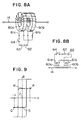
- Fig. 8A is a diagram showing an embodiment of the residual flux reset unit suited for use with the pulse generator according to the invention.
- Fig. 8B is a circuit diagram for the resetting unit of Fig. 8A.
- Fig. 9 is a diagram showing magnetic characteristics of the iron cores.
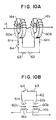
- Fig. 10A is a diagram showing another embodiment of the residual flux reset unit.
- Fig. 10B is a circuit diagram for the resetting unit of Fig. 10A.
- Fig. 11A is a diagram showing still another embodiment of the residual flux resetting unit.
- Fig. 11B is a circuit diagram for the resetting unit of Fig. 11A.
- the pulse generator designated generally with numeral 100, is connected to a laser device 102 from an LC resonant circuit 9 on the secondary side of a transformer 101 through a saturable reactor 103.
- a timing circuit 104 and a reset circuit 105 are arranged on the secondary side of the saturable reactor 103 and these circuits are also connected to a control circuit 106.
- One side of the control circuit 106 is connected to the bases B of transistors 3A and 3B which are connected to the primary winding of the transformer 101.
- the transformer 101 includes the primary winding 1 and the secondary winding 2.
- the ends of the primary winding 1 are respectively connected to the first and second transistors 3A and 3B forming switching elements.
- a lead line 4A brought out from the intermediate point of the primary winding 1 between the transistors 3A and 3B is connected to a dc power source 4.
- One end of the dc power source 4 is connected to the emitters E of the transistors 3A and 3B and a ground 5.
- the bases B of the transistors 3A and 3B are connected to the control circuit 106.
- a detecting winding 7, e.g., a current transformer, is connected to the control circuit 106 to detect the direction of current flow in the secondary winding 2.
- a capacitor 8 is connected in parallel between the ends of the secondary winding 2 to form an LC resonant circuit (tank circuit) 9.
- the LC resonant circuit 9 is connected to an output capacitor 11 and the laser device 102.
- the laser device 102 includes a discharge section 12 containing a laser gas and electrodes 12A and 12B, e.g., cathode and anode arranged within the discharge section 12.
- the ends of the electrodes 12A and 12B are connected in parallel with the output capacitor 11.
- the electrodes 12A and 12B and one end of the output capacitor 11 are connected to a ground 11E.
- the saturable reactor 103 is connected in series with one side of the electrodes 12A and 12B and the output capacitor 11 and the LC resonant circuit 9, respectively.
- the saturable reactor 103 includes an iron core, e.g., ring core 13 and a main winding 14 wound on the ring core 13, and the ends of the main winding 14 are respectively connected to the LC resonant circuit 9 and the output capacitor 11, etc.
- the timing circuit 104 and the reset circuit 105 are arranged on the secondary side (control windings) of the saturable reactor 103.
- the timing circuit 104 includes a control winding 15 wound on the core 13, a transistor 16 and a dc power source 17.
- the reset circuit 105 includes a pair of windings 20A and 20B which are wound on the core 13.
- a branch line 21 is brought out from between the windings 20A and 20B and connected to one end of a dc power source 22.
- the negative terminal of the dc power source 22 and one ends of the windings 20A and 20B are respectively connected to the emitters E and collectors C of transistors 23A and 23B.
- the emitters E are connected to a ground 24.
- the bases B of the transistors 16, 23A and 23B are connected to the control circuit 106.
- a current I s1 such as shown in (a) of Fig. 2 flows to the primary winding 1 from the dc power source 4.
- the abscissa represents the time t .
- the current I s1 induces a voltage in the secondary winding 2 electromagnetically coupled to the primary winding 1, thereby causing the flow of a current I c1 such as shown in (d) of Fig. 2.
- the capacitor 8 is connected in parallel with the secondary winding 2 to form the LC resonant circuit 9.
- the secondary current I s1 produces a secondary voltage V c1 as shown in (e) of Fig. 2.
- the detecting winding 7 detects the reversal of the current I c1 in the LC resonant circuit 9 to turn the first transistor 3A off and the second transistor 3B on through the control circuit 106.
- a current I s2 flows as shown in (b) of Fig. 2.
- the resulting voltage induced in the secondary winding 2 by the current I S2 is opposite in polarity to the induced voltage by the current I s1 .
- the current I c1 increases in magnitude each time it reverses.
- the main winding 14 of the saturable reactor 103 has a large inductance and thus a large impedance is presented to the oscillating voltage of the LC resonant circuit 9. As a result, practically no voltage appears across the capacitor 11.
- the magnetic flux within the core 13 is varied as shown by the dotted line in (e) of Fig. 2 in proportion to an time-integrated value of the voltage applied to the winding 14.
- the crossectional area of its core 13 and the number of turns of its winding 14 are preset to such values that the saturable reactor 103 is not saturated until the voltage V c1 of the LC resonant circuit 9 exceeds the desired value. As a result, the saturable reactor 103 is not saturated irrespective of time until the voltage of the LC resonant circuit 9 attains the core saturation level.
- the capacities of the first and second transistors 3A and 3B can be made small enough as compared with the case of the conventional method of supplying about one half of an electric energy to be supplied by every switching.
- the control circuit 106 detects that the voltage of the LC resonant circuit 9 has attained the desired value.
- the desired number of times of polarity reversal for the current in the secondary winding 2 of the transformer 101 has been preliminarily examined so that the detecting winding 7 detects each polarity reversal and the control circuit 106 counts the number of occurrences. when the count reaches the desired number of times of polarity reversal, the transistor 16 of the timing circuit 104 is turned on.
- Another method may be used in which the voltage V c1 is measured directly by a voltage divider to turn the transistor 16 on when the voltage V c1 reaches the desired value.
- the current flowing in the primary winding 1 opens and closes the transistors 3A and 3B so that the LC resonant circuit 9 causes LC resonance to store a large electric energy and this energy is controlled by the saturable reactor 103, thereby outputting a high voltage.
- the LC resonant circuit 9 causes LC resonance to store a large electric energy and this energy is controlled by the saturable reactor 103, thereby outputting a high voltage.
- the core 13 is saturated and the electric energy is transferred to the capacitor 11.
- the core 13 In order to transfer the maximum electric energy to the capacitor 11, the core 13 must be saturated at around the maximum voltage value of the capacitor 8.
- the transistor 16 connected to the control winding 15 is turned on to supply the current I ON from the dc power source 17.
- the main winding 14 and the control winding 15 from a transformer and thus the current I ON produces a current I c2 in the main winding 14, thereby charging the capacitor 11.
- This voltage is preset lower than the discharge initiating voltage of the laser device 102 and thus there is no danger of discharging the laser device 102.
- the voltage V c2 charged in the capacitor 11 by the current I ON charges a voltage of the opposite polarity to a voltage which is to be outputted finally.
- the voltage applied to the main winding 14 is decreased at a half wave (the A portion in (e) of Fig. 2) of the opposite polarity to the polarity of the voltage applied to the laser device 102 and thus the amount of change (the amount of decrease in this case) of the magnetic flux in the core is decreased.
- the voltage applied to the main winding 14 is increased and the amount of change of the flux in the core is increased, thereby saturating the core.
- the capacitor 11 is charged so that the resulting voltage produces a magnetic flux and this magnetic flux is utilized to saturate the core 13.
- the timing of saturating the core 13 can be adjusted in dependence on the magnitude of the voltage on the capacitor 11 or the magnitude of the current I ON flowing in the control winding 15.
- the timing circuit 104 by providing the timing circuit 104, the electric energy stored in the LC resonant circuit 9 can be outputted positively at the optimum time instant.
- the voltage V c1 of the LC resonant circuit 9 is a voltage which oscillates between positive and negative limits.
- the magnetic flux in the core 13 also oscillates between positive and negative saturation points.
- the initial value of the magnetic flux in the core 13 is reduced to substantially zero, the normal operation is performed.
- the initial value of the magnetic flux in the core 13 is dependent on the preceding discharge of the laser device 102 and it cannot always be near to zero.
- the residual voltage in the capacitor 11 varies due to variations in the discharge voltage and variations in the discharge time. As a result, variations are caused in the magnetic flux in the core 13 which is varied by the remaining voltage in the capacitor 11.
- the transistor 23A is turned on and the core 13 is saturated.
- the transistor 23A controls in such a manner that a sufficient time and current for saturating the core 13 in one direction are provided irrespective of the value of the magnetic flux in the core 13.
- the transistor 23A is turned off and the other transistor 23B is turned on, thereby energizing the core 13 in the reverse direction.
- the transistor 23B is turned off.
- the necessary current value, voltage value and applying time thereof for reducing the magnetic flux to zero has been determined preliminarily from the magnetic characteristic of the core 13.
- An induced voltage is charged in the capacitor 11 by the reset current from the control winding 20B.
- the charged voltage of the capacitor 11 also varies the magnetic flux in the core 13. Therefore, the on period of the transistor 23B for resetting the magnetic flux in the core 13 to zero is selected to have a value sufficient to reduce the total flux including the flux due to the capacitor 11.
- Figs. 8 to 11A there are illustrated another embodiments of the reset circuit in the pulse generator according to the invention.
- the resetting is effected by controlling the supply time of the reset current to the control winding.
- the present embodiment feature that the core of the saturable reactor is divided into a plurality of parts and also the single switching element is employed.
- by suitably selecting the crossectional area of each split core or by varying the number of turns of the main winding on the split cores it is possible to control the residual flux to not only zero but also any given value.
- two split cores which are saturable in different directions, it is possible to prevent the variation of any magnetic flux by the charged voltage of the output capacitor due to a reset current.
- FIG. 8A shows the reset circuit according to this embodiment.
- a saturable reactor includes an iron core splitted into two core 60a and 60b, a main winding 14 wound to extend over the split cores 60a and 60b, and control windings 61a and 61b which are respectively wound on the split cores 60a and 60b.
- a dc power source 62, a current controlling resistor 63 and a switch 64 are connected in series with the control windings 61a and 61b.
- Fig. 8B shows a circuit diagram of the reset circuit. When the switch 64 is closed, the directions of current flow in the control windings 61a and 61b are opposite to each other.
- a current i determined by the voltage of the dc power source 62 and the resistor 63 flows to the control windings 61a and 61b.
- the current i is preset to a current value sufficient for saturating the split cores 60a and 60b, respectively.
- Fig. 9 shows hysteresis curves (the solid lines) of the split cores 60a and 60b.
- the magnetic flux in the split core 60a is saturated to P and the magnetic flux in the split core 60b is saturated to Q.
- the switch 64 is opened so that the current i is reduced to zero, the residual flux in the split core 60a is reset to R and the residual flux in the split core 60b is reset to S.
- the characteristic of the cores on the whole with respect to the main winding 14 is one combining the characteristics of the split cores 60a and 60b and the corresponding hysteresis curve is shown by the dotted line in the Figure. Also, where the characteristics and crosssectional areas of the split cores 60a and 60b are the same, the residual flux becomes effectively Z or zero.
- control windings require only the single control circuit (the power source, switch, etc.). Also, the residual fluxes in the cores can be controlled partially and hence the residual fluxes can be easily reset to any given value.
- a saturable reactor includes main windings 14a and 14b which are provided separately for split cores 60a and 60b, respectively.
- the induced electromotive forces to the main windings 14a and 14b are proportional to the varying amounts of magnetic fluxes and the numbers of turns.
- Fig. 10B shows a circuit diagram for the reset circuit of Fig. 10A.
- Fig. 11A shows still another embodiment of the reset circuit according to the invention.
- a saturable reactor core is divided into three split cores 60a, 60b and 60c on which control windings 61a, 61b and 61c are respectively wound.
- a switch 65 for changing the direction of current flow is connected to the control winding 61c.
- the switch 65 By operating the switch 65, the direction of saturation of the split core 60c is reversed thereby varying the value to which the residual fluxes are reset.
- the resulting value of the residual flux can be easily varied by means of the switch 65 connected to the control winding 61c.
- Fig. 11B shows a circuit diagram of the reset circuit shown in Fig. 11A.
- the reset circuit of this embodiment can easily reset the residual fluxes in the cores to zero or any other value than the saturation region by use of the simple construction.
- switches 64 and 65 take the form of mechanical switches, it is needless to say that such switching elements as transistors may be used as in the circuit of Fig. 1.
- Fig. 3 is a block diagram showing an internal construction of the control circuit 106.
- a first timer is first brought into operation to generate a pulse signal.
- the pulse signal is amplified by a first driver circuit to turn the transistor 23A on.
- a second timer comes into operation with a delay so that a pulse signal is applied to a second driver circuit and the second drive circuit turns to transistor 23B on.
- a current flows to the control winding 20B and the magnetic flux in the core 13 is reset to zero.
- the magnetic flux including the effects of the voltages charged in the capacitors 8 and 11 by the induced voltage in the winding 14 is reset to zero.
- the residual flux in the core 13 is reset.
- a third timer comes into operation and a start signal generating circuit generates a pulse signal.
- This pulse signal is amplified by a fifth driver circuit to turn the transistor 3A on so that the capacitor 8 is charged by the current I s1 in the winding 1 and the resonant circuit 9 starts oscillating (the oscillation of voltage and current).
- the plarity reversals (oscillations) of the resonant circuit 9 are detected by the detecting winding 7 so that a pulse corresponding to each polarity is generated from an oscillation polarity detecting circuit and the transitors 3A and 3B are alternately turned on and off, thereby increasing the oscillating voltage and current of the resonant circuit 9.
- a fourth timer comes into operation and generates a pulse so that the transistor 16 is turned on and the saturable reactor 103 is saturated, thereby supplying the energy in the resonant circuit 9 to the capacitor 11.
- the embodiment of Fig. 4 differs from the embodiment of Fig. 1 in that the capacitor 11 is charged directly from the dc power source 17 by means of the transistor 16.
- the transistor 16 and the dc power source 17 are protected from the high voltage by a surge absorving circuit 30 including resistors 26 and 29, a diode 28 and a capacitor 27.
- FIG. 5 there is illustrated still another embodiment of the pulse generator according to the invention, which differs from the embodiment of Fig. 1 in that a magnetic pulse compression circuit 40 is provided between the saturable reactor 103 and the reset circuit 105 and the laser device 102.
- the magnetic pulse compression circuit 40 includes a saturable reactor 103 ⁇ and a capacitor 43 and it has the following functions and effects.
- the current I ON shown in (c) of Fig. 2 is supplied to the main winding 14 so that the capacitor 11 is charged by the current I ON and the sawtooth wave V c2 ⁇ shown in (f) of Fig. 2 is produced, thereby saturating the core 13.
- the voltage V c2 ⁇ is preset near to the discharge voltage so as to saturate the saturable reactor 103 in a short period of time, the danger of the laser device 102 being caused to malfunction due to the voltage V c2 ⁇ is conceivable.
- FIG. 6 there is illustrated still another embodiment of the pulse generator according to the invention which differs from the embodiment of Fig. 1 in that a core 50 is arranged between the primary and secondary windings 1 and 2 of the transformer 101.
- a resonant circuit is provided by utilizing the reversion of the voltage on the capacitor 8 due to the saturation of the core 50 of the transformer 101.
- a current I s1 flow to the primary winding 1 wound on the core 50 from the dc power source 4 as shown in (a) of Fig. 7. Since the primary and secondary windings 1 and 2 are magnetically coupled through the core 50 thus forming the transformer 101, the current I s1 causes the flow of a current I c1 in the secondary winding 2 as shown in (c) of Fig. 7. The current I c1 flows to the capacitor 8 thereby producing a voltage V c1 on the capacitor 8 as shown in (d) of Fig. 7. The voltage V c1 increases the magnetic flux in the core 50 to vary as shown by the dotted line in (d) of Fig. 7.
- the voltage V c1 is also applied to the winding 14 so that the magnetic flux in the core 13 is also increased to vary as shown in (e) of Fig. 7. Then, since the voltage-time products for transformer 101 and the saturable reactor 103 have been preset to become Z1 ⁇ Z2 as shown by equation (3), the core 50 is saturated first and the inductance of the secondary winding 2 is decreased. The charge in the capacitor 8 is discharge through the secondary winding 2 at a frequency determined by the descreased inductance and the capacitance of the capacitor 8 and a half cycle of the discharge current in (A in (c) of Fig. 7) flows. As a result, the polarity of the voltage on the capacitor 8 is reversed. When this occurs, the magnetic fluxes in the cores 13 and 50 begin to vary in the reverse direction.
- the discharge current I c1 or A of the capacitor 8 is detected by the detecting winding 7 so that the transistor 3A is turned off and the transistor 3B is turned on by the control circuit 106. Consequently, the capacitor 8 is charged in the opposite polarity to previously by the primary winding 1 and the dc power source 4 and its stored electric energy is increased.
- the capacitor 8 is again discharged and the polarity reversal of its voltage is caused. As a result, the on and off states of the transistors 3A and 3B are also reversed thereby charging the capacitor 8.
- the transistors 3A and 3B are turned on and off in accordance with the polarity of the voltage on the capacitor 8 so that the voltage on the capacitor 8 is increased and its electric energy is increased.
- the voltage waveform Z appearing on the capacitor 8 has a rectangular waveform and thus the electric energy of the output voltage is substantially constant even if the timing of saturating the saturable reactor 103 is varied more or less.
Landscapes
- Physics & Mathematics (AREA)
- Electromagnetism (AREA)
- Nonlinear Science (AREA)
- Engineering & Computer Science (AREA)
- Plasma & Fusion (AREA)
- Optics & Photonics (AREA)
- Lasers (AREA)
- Generation Of Surge Voltage And Current (AREA)
Description
- The invention relates to an apparatus and to a method of generating high-voltage pulses for supplying high voltage pulses to a laser device.
- Laser devices of the transversely excited atmospheric pressure (TEAP) type have required high-voltage pulses of a short rise time. In the past, a pulse generating circuit of this type has been disclosed in DE-A-33 35 690. This pulse generating circuit is designed so that one of two parallelly charged capacitors is discharged through an inductance to invert the voltage of the discharged capacitor and combine it with the voltage of the other capacitor thereby producing a voltage which is two times the charged voltage and also a saturable reactor is saturated to take out as an output the electric energy stored in the capacitors. Thus, there is a need for a large-capacity switching element capable of switching at a time about half the electric energy to be outputted during the discharging of said one capacitor. Moreover, the capacity of the switching element or the saturable reactor is increased in inverse proportion to the rise time of the output pulse. Also, while the number or capacity of the following stages in the pulse generating circuit may be increased to decrease the capacity of the switching element, this method has the disadvantage of increasing the number of capacitors and the saturable reactors and of increasing the size of the pulse generating circuit with the resulting increase in the cost and the like.
- US-A-3 211 915 discloses a circuit with the structural features as defined in the preamble of claim 1, which is definitely suited for supplying high-voltage pulses to a laser device.
- With a view to overcome the foregoing deficiencies in the prior art, it is an object of the present invention to provide a high-voltage pulse generator and a method of generating high-voltage pulses with small-capacity switching elements for supplying said pulses to a laser device.
- These objects are achieved by the invention according to a first aspect by the features recited in claim 1 and according to a second aspect by the features recited in
claim 13. - In the high-voltage pulse generator according to the invention, the switches connected to the primary winding of the transformer are opened and closed plural times in synchronism with the electric oscillation of the resonant circuit on the transformer secondary side so that the electric energy stored in the resonant circuit is increased and the saturable reactor is saturated by the voltage of the resonant circuit, thus outputting the electric energy stored in the resonant circuit and thereby causing the output capacitor to generate a high-voltage pulse having a short rise time and a large energy. In other words, although the electric energy controlled by the primary winding is small, this electric energy is stored plural times in the resonant circuit and eventually electric energy is generated which is several tens times the electric energy controlled by the primary winding. Thus, the capacity of the primary-side switching elements is reduced thereby making it easy the utilization of switching semiconductor elements and the switching of the large energy is effected by the saturable reactor with the resulting increased size and increased life for the device.
- Other objects of the invention will become apparent from the following description of preferred embodiments taken in conjunction with the accompanying drawings.
- Fig. 1 is a circuit diagram of a pulse generator for lasers according to an embodiment of the invention.
- Figs. 2(a) to (h) shown a plurality of signal waveforms generated at various parts of Fig. 1.
- Fig. 3 is a block diagram of the control circuit which is applicable to the pulse generators shown in Figs. 1, 4 and 5, respectively.
- Figs. 4 to 6 are circuit diagrams showing pulse generators for lasers according to another embodiments of the invention.
- Figs. 7(a) to (g) show a plurality of signal waveforms generated at various parts in the circuit of Fig. 6.
- Fig. 8A is a diagram showing an embodiment of the residual flux reset unit suited for use with the pulse generator according to the invention.
- Fig. 8B is a circuit diagram for the resetting unit of Fig. 8A.
- Fig. 9 is a diagram showing magnetic characteristics of the iron cores.
- Fig. 10A is a diagram showing another embodiment of the residual flux reset unit.
- Fig. 10B is a circuit diagram for the resetting unit of Fig. 10A.
- Fig. 11A is a diagram showing still another embodiment of the residual flux resetting unit.
- Fig. 11B is a circuit diagram for the resetting unit of Fig. 11A.
- A first embodiment of a pulse generator according to the invention will be described with reference to Fig. 1.
- The pulse generator, designated generally with
numeral 100, is connected to alaser device 102 from anLC resonant circuit 9 on the secondary side of atransformer 101 through asaturable reactor 103. Atiming circuit 104 and areset circuit 105 are arranged on the secondary side of thesaturable reactor 103 and these circuits are also connected to acontrol circuit 106. One side of thecontrol circuit 106 is connected to the bases B oftransistors transformer 101. - The
transformer 101 includes the primary winding 1 and thesecondary winding 2. The ends of the primary winding 1 are respectively connected to the first andsecond transistors lead line 4A brought out from the intermediate point of the primary winding 1 between thetransistors dc power source 4. One end of thedc power source 4 is connected to the emitters E of thetransistors ground 5. The bases B of thetransistors control circuit 106. A detecting winding 7, e.g., a current transformer, is connected to thecontrol circuit 106 to detect the direction of current flow in thesecondary winding 2. Acapacitor 8 is connected in parallel between the ends of thesecondary winding 2 to form an LC resonant circuit (tank circuit) 9. TheLC resonant circuit 9 is connected to anoutput capacitor 11 and thelaser device 102. - The
laser device 102 includes adischarge section 12 containing a laser gas andelectrodes discharge section 12. The ends of theelectrodes output capacitor 11. Theelectrodes output capacitor 11 are connected to a ground 11E. Thesaturable reactor 103 is connected in series with one side of theelectrodes output capacitor 11 and theLC resonant circuit 9, respectively. - The
saturable reactor 103 includes an iron core, e.g.,ring core 13 and a main winding 14 wound on thering core 13, and the ends of the main winding 14 are respectively connected to theLC resonant circuit 9 and theoutput capacitor 11, etc. Thetiming circuit 104 and thereset circuit 105 are arranged on the secondary side (control windings) of thesaturable reactor 103. - The
timing circuit 104 includes a control winding 15 wound on thecore 13, atransistor 16 and adc power source 17. - The
reset circuit 105 includes a pair ofwindings core 13. Abranch line 21 is brought out from between thewindings dc power source 22. The negative terminal of thedc power source 22 and one ends of thewindings transistors ground 24. - The bases B of the
transistors control circuit 106. - Next, the operation of the
pulse generator 100 will be described with reference to Fig. 2. - When the
first transistor 3A is turned on by the drive signal from thecontrol circuit 106, a current Is1 such as shown in (a) of Fig. 2 flows to the primary winding 1 from thedc power source 4. In (a) to (h) of Fig. 2, the abscissa represents the time t. The current Is1 induces a voltage in the secondary winding 2 electromagnetically coupled to the primary winding 1, thereby causing the flow of a current Ic1 such as shown in (d) of Fig. 2. Thecapacitor 8 is connected in parallel with the secondary winding 2 to form the LCresonant circuit 9. The secondary current Is1 produces a secondary voltage Vc1 as shown in (e) of Fig. 2. The detecting winding 7 detects the reversal of the current Ic1 in the LCresonant circuit 9 to turn thefirst transistor 3A off and thesecond transistor 3B on through thecontrol circuit 106. When this occurs, a current Is2 flows as shown in (b) of Fig. 2. The resulting voltage induced in the secondary winding 2 by the current IS2 is opposite in polarity to the induced voltage by the current Is1. As will be seen from Fig. 2(d), the current Ic1 increases in magnitude each time it reverses. In this way, by turning the first andsecond transistors resonant circuit 9, an electric energy is injected into the LCresonant circuit 9 and the oscillating frequency and voltage are increased. In other words, the electric energy stored in the LCresonant circuit 9 is increased. - On the other hand, as far as the
core 13 is not saturated, the main winding 14 of thesaturable reactor 103 has a large inductance and thus a large impedance is presented to the oscillating voltage of the LCresonant circuit 9. As a result, practically no voltage appears across thecapacitor 11. On the other hand, the magnetic flux within thecore 13 is varied as shown by the dotted line in (e) of Fig. 2 in proportion to an time-integrated value of the voltage applied to the winding 14. With thesaturable reactor 103, the crossectional area of itscore 13 and the number of turns of its winding 14 are preset to such values that thesaturable reactor 103 is not saturated until the voltage Vc1 of the LCresonant circuit 9 exceeds the desired value. As a result, thesaturable reactor 103 is not saturated irrespective of time until the voltage of the LCresonant circuit 9 attains the core saturation level. - In other words, there is no restriction to the time required for storing the desired voltage energy in the LC
resonant circuit 9. It is only necessary that an electric energy to be supplied to the LCresonant circuit 9 by switching the first andsecond transistors resonant circuit 9 and they are sufficiently small as compared with an electric energy which is to be finally stored in the LCresonant circuit 9. To store a large energy in the resonant circuit in a short time, it is necessary to use large-capacity switching elements for the purpose of increasing an energy to be supplied by every switching. Conversely, when such energy is to be stored in a long period of time, the capacities of the elements can be made smaller. - Therefore, the capacities of the first and
second transistors - When the voltage of the LC
resonant circuit 9 attains the desired value, thetransistor 16 is turned on and a current ION such as shown in (c) of Fig. 2 flows to the control winding 15 from thedc power source 17. The corresponding current (Ic2) to the current ION flows to the main winding 14 so that thecapacitor 11 is charged and a voltage Vc2ʹ is generated as shown in (f) of Fig. 2. Thecore 13 is saturated by the voltage Vc2ʹ so that the inductance of the winding 14 is decreased and the impedance is reduced. When this occurs, the charge stored in thecapacitor 8 is discharged and the current Ic2 flows as shown in (g) of Fig. 2. When the voltage applied to thecapacitor 11 is increased thus reaching the voltage for initiating the discharge of thelaser device 102, the impedance of thedischarge section 12 is decreased rapidly and the charges are discharged from thecapacitors discharge section 12. Thus, a current ID combining the currents from thecapacitors laser device 102 and it takes the form of a pulse having a rapid positive transition as shown in (h) of Fig. 2. - It is to be noted that to determine the timing of saturation of the
saturable reactor 103, thecontrol circuit 106 detects that the voltage of the LCresonant circuit 9 has attained the desired value. The desired number of times of polarity reversal for the current in the secondary winding 2 of thetransformer 101 has been preliminarily examined so that the detecting winding 7 detects each polarity reversal and thecontrol circuit 106 counts the number of occurrences. when the count reaches the desired number of times of polarity reversal, thetransistor 16 of thetiming circuit 104 is turned on. Another method may be used in which the voltage Vc1 is measured directly by a voltage divider to turn thetransistor 16 on when the voltage Vc1 reaches the desired value. - In this way, the current flowing in the primary winding 1 opens and closes the
transistors resonant circuit 9 causes LC resonance to store a large electric energy and this energy is controlled by thesaturable reactor 103, thereby outputting a high voltage. Thus, it is only necessary to flow a small current a plurality of times to the primary winding and this permits the use of small-capacity transistors, thereby reducing the size of the pulse generator. - To supply a pulse voltage to the
laser device 102, it is necessary that after the desired electric energy has been charged in the LCresonant circuit 9, thecore 13 is saturated and the electric energy is transferred to thecapacitor 11. In order to transfer the maximum electric energy to thecapacitor 11, the core 13 must be saturated at around the maximum voltage value of thecapacitor 8. For this purpose, thetransistor 16 connected to the control winding 15 is turned on to supply the current ION from thedc power source 17. The main winding 14 and the control winding 15 from a transformer and thus the current ION produces a current Ic2 in the main winding 14, thereby charging thecapacitor 11. This voltage is preset lower than the discharge initiating voltage of thelaser device 102 and thus there is no danger of discharging thelaser device 102. - The voltage Vc2 charged in the
capacitor 11 by the current ION charges a voltage of the opposite polarity to a voltage which is to be outputted finally. As a result of this, the voltage applied to the main winding 14 is decreased at a half wave (the Ⓐ portion in (e) of Fig. 2) of the opposite polarity to the polarity of the voltage applied to thelaser device 102 and thus the amount of change (the amount of decrease in this case) of the magnetic flux in the core is decreased. Also, in the range of the same polarity as the applied voltage (the Ⓑ portion in (e) of Fig. 2), the voltage applied to the main winding 14 is increased and the amount of change of the flux in the core is increased, thereby saturating the core. In other words, thecapacitor 11 is charged so that the resulting voltage produces a magnetic flux and this magnetic flux is utilized to saturate thecore 13. Thus, the timing of saturating the core 13 can be adjusted in dependence on the magnitude of the voltage on thecapacitor 11 or the magnitude of the current ION flowing in the control winding 15. - By adjusting the timing of saturation of the core 13, a large part of the electric energy stored in the LC
resonant circuit 9 is transferred to the output side. - Consequently, by providing the
timing circuit 104, the electric energy stored in the LCresonant circuit 9 can be outputted positively at the optimum time instant. - Next, the
reset circuit 105 will be described. - More specifically, the voltage Vc1 of the LC
resonant circuit 9 is a voltage which oscillates between positive and negative limits. In accordance with this oscillating voltage, the magnetic flux in the core 13 also oscillates between positive and negative saturation points. Where the initial value of the magnetic flux in thecore 13 is reduced to substantially zero, the normal operation is performed. However, the initial value of the magnetic flux in thecore 13 is dependent on the preceding discharge of thelaser device 102 and it cannot always be near to zero. In other words, after the discharging operation, the residual voltage in thecapacitor 11 varies due to variations in the discharge voltage and variations in the discharge time. As a result, variations are caused in the magnetic flux in the core 13 which is varied by the remaining voltage in thecapacitor 11. - If the initial value of the magnetic flux in the
core 13 deviates from the vicinity of zero, there is the danger of the core 13 being saturated before the electric energy of the LCresonant circuit 9 attaining the desired value and the normal operation is not performed. Therefore, the residual flux of the core 13 must be reset to zero. - For this purpose, in the
reset circuit 105 of this invention, thetransistor 23A is turned on and thecore 13 is saturated. Thetransistor 23A controls in such a manner that a sufficient time and current for saturating the core 13 in one direction are provided irrespective of the value of the magnetic flux in thecore 13. Then, thetransistor 23A is turned off and theother transistor 23B is turned on, thereby energizing the core 13 in the reverse direction. When the magnetic flux is reduced to zero, thetransistor 23B is turned off. - The necessary current value, voltage value and applying time thereof for reducing the magnetic flux to zero has been determined preliminarily from the magnetic characteristic of the
core 13. An induced voltage is charged in thecapacitor 11 by the reset current from the control winding 20B. The charged voltage of thecapacitor 11 also varies the magnetic flux in thecore 13. Therefore, the on period of thetransistor 23B for resetting the magnetic flux in the core 13 to zero is selected to have a value sufficient to reduce the total flux including the flux due to thecapacitor 11. By so doing, the initial value of the core magnetic flux is always maintained at near to zero so that thesaturable reactor 103 is always saturated by a constant voltage-time product and the pulsing operation of the pulse generator is always stabilized. - Referring now to Figs. 8 to 11A, there are illustrated another embodiments of the reset circuit in the pulse generator according to the invention. In the previously mentioned embodiment of the reset circuit, the resetting is effected by controlling the supply time of the reset current to the control winding. The present embodiment feature that the core of the saturable reactor is divided into a plurality of parts and also the single switching element is employed. In accordance with this embodiment, by suitably selecting the crossectional area of each split core or by varying the number of turns of the main winding on the split cores, it is possible to control the residual flux to not only zero but also any given value. In addition, by using two split cores which are saturable in different directions, it is possible to prevent the variation of any magnetic flux by the charged voltage of the output capacitor due to a reset current.
- Fig. 8A shows the reset circuit according to this embodiment. A saturable reactor includes an iron core splitted into two
core split cores split cores dc power source 62, a currentcontrolling resistor 63 and aswitch 64 are connected in series with the control windings 61a and 61b. Fig. 8B shows a circuit diagram of the reset circuit. When theswitch 64 is closed, the directions of current flow in the control windings 61a and 61b are opposite to each other. - In response to the closing of the
switch 64, a current i determined by the voltage of thedc power source 62 and theresistor 63 flows to the control windings 61a and 61b. The current i is preset to a current value sufficient for saturating thesplit cores - Fig. 9 shows hysteresis curves (the solid lines) of the
split cores split core 60a is saturated to P and the magnetic flux in thesplit core 60b is saturated to Q. When theswitch 64 is opened so that the current i is reduced to zero, the residual flux in thesplit core 60a is reset to R and the residual flux in thesplit core 60b is reset to S. - The characteristic of the cores on the whole with respect to the main winding 14 is one combining the characteristics of the
split cores split cores - Consider the operations performed in response to the application of a voltage to the main winding 14. Firstly, when the voltage is applied to the main winding 14 in a direction which increases the magnetic fluxes in the
split cores split core 60a is in the saturated state in this direction and the magnetic flux is not increased. On the other hand, as will be seen from Fig. 9, it is possible for thesplit core 60b to increase the magnetic flux between the points S and P and therefore the magnetic flux is increased in proportion to the applied voltage. This increase in the magnetic flux results in an increase in the inductance of the main winding 14. When a voltage of the opposite polarity is applied, the magnetic flux in thesplit core 60a is decreased and thus the inductance of the main winding 14 is increased. The results of these operations are the same as the case where the residual fluxes in thesplit cores - The result obtained by thus resetting the residual fluxes in the
split cores split cores - The description has been made of the case where the characteristics and crosssectional areas of the
split cores split cores - Thus, in accordance with the present embodiment, the control windings require only the single control circuit (the power source, switch, etc.). Also, the residual fluxes in the cores can be controlled partially and hence the residual fluxes can be easily reset to any given value.
- Referring now to Fig. 10A, there is illustrated still another embodiment of the reset circuit. In this embodiment, a saturable reactor includes
main windings split cores main windings main windings split cores - Fig. 11A shows still another embodiment of the reset circuit according to the invention. In this embodiment, a saturable reactor core is divided into three
split cores control windings 61a, 61b and 61c are respectively wound. Aswitch 65 for changing the direction of current flow is connected to the control winding 61c. By operating theswitch 65, the direction of saturation of thesplit core 60c is reversed thereby varying the value to which the residual fluxes are reset. Thus, in accordance with this embodiment, the resulting value of the residual flux can be easily varied by means of theswitch 65 connected to the control winding 61c. Fig. 11B shows a circuit diagram of the reset circuit shown in Fig. 11A. - As described hereinabove, the reset circuit of this embodiment can easily reset the residual fluxes in the cores to zero or any other value than the saturation region by use of the simple construction.
- While, in the above-described embodiments, the
switches - The
control circuit 106 of Fig. 1 will now be described in greater detail. Fig. 3 is a block diagram showing an internal construction of thecontrol circuit 106. - In response to an externally applied trigger signal, a first timer is first brought into operation to generate a pulse signal. The pulse signal is amplified by a first driver circuit to turn the
transistor 23A on. When this occurs, a current flows to the control winding 20A and thecore 13 is saturated. A second timer comes into operation with a delay so that a pulse signal is applied to a second driver circuit and the second drive circuit turns totransistor 23B on. Thus, a current flows to the control winding 20B and the magnetic flux in thecore 13 is reset to zero. (The magnetic flux including the effects of the voltages charged in thecapacitors core 13 is reset. Then, a third timer comes into operation and a start signal generating circuit generates a pulse signal. This pulse signal is amplified by a fifth driver circuit to turn thetransistor 3A on so that thecapacitor 8 is charged by the current Is1 in the winding 1 and theresonant circuit 9 starts oscillating (the oscillation of voltage and current). The plarity reversals (oscillations) of theresonant circuit 9 are detected by the detecting winding 7 so that a pulse corresponding to each polarity is generated from an oscillation polarity detecting circuit and thetransitors resonant circuit 9. - Then, at the expiration of a given time after the reception of the output pulse of the third timer, a fourth timer comes into operation and generates a pulse so that the
transistor 16 is turned on and thesaturable reactor 103 is saturated, thereby supplying the energy in theresonant circuit 9 to thecapacitor 11. - Next, another embodiment of the pulse generator according to the invention will be described with reference to Fig. 4.
- The embodiment of Fig. 4 differs from the embodiment of Fig. 1 in that the
capacitor 11 is charged directly from thedc power source 17 by means of thetransistor 16. In this circuit, when the electric energy in thecapacitor 8 is transferred to thecapacitor 11 thereby producing a high voltage, thetransistor 16 and thedc power source 17 are protected from the high voltage by asurge absorving circuit 30 includingresistors diode 28 and acapacitor 27. - Referring to Fig. 5, there is illustrated still another embodiment of the pulse generator according to the invention, which differs from the embodiment of Fig. 1 in that a magnetic
pulse compression circuit 40 is provided between thesaturable reactor 103 and thereset circuit 105 and thelaser device 102. The magneticpulse compression circuit 40 includes a saturable reactor 103ʹ and acapacitor 43 and it has the following functions and effects. - In other words, in the previously mentioned
timing circuit 104, the current ION shown in (c) of Fig. 2 is supplied to the main winding 14 so that thecapacitor 11 is charged by the current ION and the sawtooth wave Vc2ʹ shown in (f) of Fig. 2 is produced, thereby saturating thecore 13. If the voltage Vc2ʹ is preset near to the discharge voltage so as to saturate thesaturable reactor 103 in a short period of time, the danger of thelaser device 102 being caused to malfunction due to the voltage Vc2ʹ is conceivable. - Thus, in accordance with this embodiment, while the charge in the
capacitor 8 is discharged and the discharge current flows to thecapacitor 11 when thecore 13 is saturated by the voltage Vc2 thus decreasing the impedance of the main winding 14, acore 41 is not saturated and the discharge is prevented by the saturable reactor 103ʹ. As the time passes so that the potential of thecapacitor 11 is increased, thecore 41 is saturated so that the charge in thecapacitor 11 is discharged and the discharge current flows to thecapacitor 43 through a main winding 42. The previosuly mentioned sawtooth voltage does not appear across thecapacitor 43. Thus, only the desired final voltage is applied to thelaser device 102, thereby preventing any malfunction. The other parts of the circuit and the same in operation with their counterparts of Fig. 1 and their explanation will be omitted. - Referring to Fig. 6, there is illustrated still another embodiment of the pulse generator according to the invention which differs from the embodiment of Fig. 1 in that a
core 50 is arranged between the primary andsecondary windings 1 and 2 of thetransformer 101. In this embodiment, a resonant circuit is provided by utilizing the reversion of the voltage on thecapacitor 8 due to the saturation of thecore 50 of thetransformer 101. - With the
transformer 101, if Z₁ represents the product of the saturation flux density B₁ and crosssectional area A₁ of thecore 50 and the number of turns N₁ of the secondary winding 2, the following equation holds

With thesaturable reactor 103, if Z₂ represents the product of the saturation flux density B₂ and crosssectional area A₂ of thecore 13 and the number of turns N₂ of the winding 14, then the following equation holds
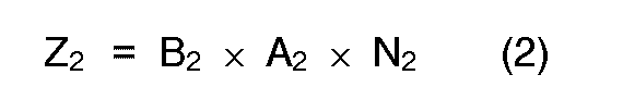
Then, assume the following conditions of Z₁ and Z₂

Thus, thetiming circuit 104 of Fig. 1 can be eliminated. The reason for this will now be described. - When the
transistor 3A is turned on, a current Is1 flow to the primary winding 1 wound on the core 50 from thedc power source 4 as shown in (a) of Fig. 7. Since the primary andsecondary windings 1 and 2 are magnetically coupled through the core 50 thus forming thetransformer 101, the current Is1 causes the flow of a current Ic1 in the secondary winding 2 as shown in (c) of Fig. 7. The current Ic1 flows to thecapacitor 8 thereby producing a voltage Vc1 on thecapacitor 8 as shown in (d) of Fig. 7. The voltage Vc1 increases the magnetic flux in the core 50 to vary as shown by the dotted line in (d) of Fig. 7. The voltage Vc1 is also applied to the winding 14 so that the magnetic flux in thecore 13 is also increased to vary as shown in (e) of Fig. 7. Then, since the voltage-time products fortransformer 101 and thesaturable reactor 103 have been preset to become Z₁ < Z₂ as shown by equation (3), thecore 50 is saturated first and the inductance of the secondary winding 2 is decreased. The charge in thecapacitor 8 is discharge through the secondary winding 2 at a frequency determined by the descreased inductance and the capacitance of thecapacitor 8 and a half cycle of the discharge current in (Ⓐ in (c) of Fig. 7) flows. As a result, the polarity of the voltage on thecapacitor 8 is reversed. When this occurs, the magnetic fluxes in thecores - The discharge current Ic1 or Ⓐ of the
capacitor 8 is detected by the detecting winding 7 so that thetransistor 3A is turned off and thetransistor 3B is turned on by thecontrol circuit 106. Consequently, thecapacitor 8 is charged in the opposite polarity to previously by the primary winding 1 and thedc power source 4 and its stored electric energy is increased. When the magnetic flux in thecore 50 is increased so that thecore 50 is eventually saturated, thecapacitor 8 is again discharged and the polarity reversal of its voltage is caused. As a result, the on and off states of thetransistors capacitor 8. - In this way, the
transistors capacitor 8 so that the voltage on thecapacitor 8 is increased and its electric energy is increased. - On the other hand, when the
core 50 is saturated so that thecapacitor 8 is discharged through the secondary winding 2 and its voltage polarity is reversed, the voltage in this interval (Ⓑ (hatched portion) in (d) of Fig. 7) has no effect on the increase and decrease of the magnetic flux in the core 50 but the magnetic flux in thecore 13 is varied. In order words, the voltage in longer interval corresponding to the voltage-time products during this interval is additionally applied to the winding 14. Then, the voltage-time product due to this voltage is increased in proportion to the voltage charged in thecapacitor 8. When the voltage-time product is increased so that is becomes greater than the difference between the voltage-time product (Z₁) of thetransformer 101 and the voltage-time product (Z₂) of thesaturable reactor 103, thecore 13 is also saturated. - When the
core 13 is saturated, the inductance of the winding 14 is decreased so that a part of the charge in thecapacitor 8 is transferred to thecapacitor 11 at a frequency determined by the decreased inductance, thecapacitor 8 and thecapacitor 11. In other words, the current Ic2 shown in (e) of Fig. 7 flows to thecapacitor 11 to produce a voltage Vc2 (shown in (f) of Fig. 7) thereon. During the next half cycle, this voltage (Ⓒ in (f) of Fig. 7) acts to further saturate the core 13 so that when thecore 13 is saturated next, a higher reverse polarity voltage (Ⓓ in (f) of Fig. 7) is produced and eventually a large part of the charge in thecapacitor 8 is transferred to thecapacitor 11. In other words, the desired voltage and current are obtained. The operations such as the discharge of the laser device due to the desired voltage are the same as in the case of Fig. 1 and will not be described here. - From the foregoing description it will be seen that in accordance with the present invention, by connecting the core 50 to the secondary winding 2 and presetting to hold the following
Z₁ < Z₂
where Z₁ represents the voltage-time product of thecore 50 and Z₂ represents the voltage-time product of thesaturable reactor 103 formed by thecore 13 and the winding 14, there is no need to use any switching element for saturating thecore 13. Also, the primary andsecondary windings 1 and 2 are electromagnetically coupled through the core and thus thecapacitor 8 can be charged efficiently. - Further, the voltage waveform Z appearing on the
capacitor 8 has a rectangular waveform and thus the electric energy of the output voltage is substantially constant even if the timing of saturating thesaturable reactor 103 is varied more or less.
Claims (14)
- A high-voltage pulse generator (100) for supplying high-voltage pulses to a laser device (102) comprising
a dc power source (4);
switching means (3A, 3B) for switching on and off a voltage from said power source (4);
a transformer (101) including a primary winding (1) and a secondary winding (2), said primary winding (1) being connected to said switching means (3A, 3B);
a tank circuit (9) including said secondary winding (2) of said transformer and a capacitor (8) connected to both ends of said secondary winding (2);
a saturable reactor (103) having a main winding (14) connected to said tank circuit (9); and
magnetic flux reset means (105) for supplying a current to control windings (20A, 20B) of said saturable reactor (103) to substantially remove a residual flux in said saturable reactor (103),
characterized in that
said switching means (3A, 3B) switches on and off the voltage from said power source (4) at an oscillation period of said tank circuit (9), whereby an electric energy from said power source (4) is stored in the form of electric oscillations; and
an output capacitor (11) is connected to the saturable reactor (103) in parallel to said laser device (102), whereby, when said main winding (14) of said saturable reactor (103) is energized, the electric energy stored in said tank circuit (9) is charged in the form of a charge energy and said charge energy is discharged as a pulse to said laser device (102). - A high-voltage pulse generator according to claim 1, wherein said magnetic flux reset means (105) further include a second dc power source (22), and second switching means (23A, 23B) connected between said second power source (22) and said control windings. (20A, 20B), whereby said second switching means (23A, 23B) is operated in a manner that a current is supplied from said second dc power source (22) in one direction of said control windings (20A, 20B) until said saturable reactor (103) is saturated and a given current is supplied in the other direction of said control windings (20A, 20B) to substantially reduce the residual magnetic flux in said saturable reactor (103) to Zero.
- A high-voltage pulse generator according to claim 2, wherein the control windings of said magnetic flux reset means (105) includes two windings (20A, 20B), wherein said second switching means includes two transistors (23A, 23B), and wherein each of said transistors (23A, 23B) is connected in series with said control windings (20A, 20B) and said second dc power source (22) such that the directions of current flow in said control windings (20A, 20B) are opposite to each other.
- A high-voltage pulse generator according to claim 3, wherein said saturable reactor (103) includes at least two split cores (60a, 60b) magnetically coupled with each other, wherein said magnetic flux reset means (105) includes at least two control windings (61a, 61b) each thereof being wound on one of said split cores (60a, 60b), and wherein a current is supplied to at least one of said control windings (61a, 61b) to saturate said one split core (60a or 60b) in the opposite direction to that of the other of said control windiings (61a,61b).
- A high-voltage pulse generator according to claim 4, wherein the main winding (14) of said saturable reactor (103) is wound with a predetermined number of turns on each of said split cores (60a,60b).
- A high-voltage pulse generator according to claim 4, wherein a switch (64) is connected to at least one of the control windings (61a, 61b) of said saturable reactor (103) to selectively change the direction of current flow therein to either the same direction or the opposite direction to the direction of current flow in the other of said control windings (61a, 61b).
- A high-voltage pulse generator according to claim 1, further comprising a saturation timing control circuit (104) for controlling the timing of energizing said saturable reactor (103).
- A high-voltage pulse generator according to claim 7, wherein said saturation timing control circuit (104) includes a further control winding (15) provided on said saturable reactor (103), and current control means (16, 17, 106) for supplying a current to said further control winding (15) to saturate said saturable reactor (103).
- A high-voltage pulse generator according to claim 8, wherein said current control means of said saturation timing control circuit (104) includes counting means (106) for counting the number of times of polarity reversal of the voltage across the secondary winding (92) of said transformer (101), and a current generating circuit (16, 17) responsive to the counting of a predetermined number of times by said counting means (106) to supply to said further control winding (15) a current for saturating said saturable reactor (103).
- A high-voltage pulse generator according to claim 7, wherein said saturation timing control circuit (104) includes counting means (106) for counting the number of times of polarity reversal of the voltage across the secondary winding (2) of said transformer (101), and a charging circuit (15, 16, 17) responsive to the counting of a predetermined number of times by said counting means (106) to charge said output capacitor (11) and thereby saturate said saturable reactor (103).
- A high-voltage pulse generator according to claim 1, wherein said transformer (101) includes an iron core (15), and wherein the following relation is satisfied

wherein B₁ represents a saturation flux density of said iron core (50), A₁ represents a crosssectional area of said iron core (50), N₁ represents the number of turns in said secondary winding (2), B₂ represents a saturation flux density of the core (13) of said saturable reactor (103), A₂ represents a crosssectional area of said reactor core (13), and N₂ represents the number of turns in said main winding (14). - A high-voltage pulse generator according to claim 1, further comprising a second saturable reactor (103') connected in series between said saturable reactor (103) and said discharge-type load (102), and a second output capacitor (43) connected in parallel with said discharge-type load (102).
- A method of generating high-voltage pulses for supplying said pulses to a laser device (102), comprising the step of
switching on and off a supply voltage of a dc power source (4) to supply a current to a primary winding of a transformer (101), said transformer having a secondary winding (2) connected with its two ends to a capacitor (8), thereby forming a tank circuit (9),
characterized by the following steps:
supplying an electric energy of said supply voltage switched on and off to said tank circuit (9) through said transformer (101), said supply voltage being switched on and off in synchronism with an oscillation frequency of said tank circuit (9);
storing said electric energy supplied to said tank circuit (9) in the form of electric oscillations;
charging an output capacitor (11), connected in parallel to said laser device (102), by switching a core of a saturable reactor (103) into saturation when the voltage of said oscillations in said tank circuit (9) attains a predetermined value,
whereby the charging current flows from said tank circuit (9) through a main winding (14) of said saturable reactor (103); and
rapidly discharging the energy stored in said output capacitor (11) and in said tank circuit (9) by initiating the discharge of said laser device (102) when the voltage on said output capacitor (11) reaches the voltage for initiating the discharge of said laser device (102). - A method according to claim 13, wherein said method further comprises the step of removing a residual flux in said saturable reactor (103) by supplying a current through a control winding (20A, 20B) of said saturable reactor (103).
Applications Claiming Priority (4)
| Application Number | Priority Date | Filing Date | Title |
|---|---|---|---|
| JP226029/86 | 1986-09-26 | ||
| JP22602986 | 1986-09-26 | ||
| JP71534/87 | 1987-03-27 | ||
| JP62071534A JPS63239808A (en) | 1987-03-27 | 1987-03-27 | Iron core reset device |
Publications (3)
| Publication Number | Publication Date |
|---|---|
| EP0261663A2 EP0261663A2 (en) | 1988-03-30 |
| EP0261663A3 EP0261663A3 (en) | 1989-07-12 |
| EP0261663B1 true EP0261663B1 (en) | 1992-06-17 |
Family
ID=26412631
Family Applications (1)
| Application Number | Title | Priority Date | Filing Date |
|---|---|---|---|
| EP19870113913 Expired - Lifetime EP0261663B1 (en) | 1986-09-26 | 1987-09-23 | Laser device with high-voltage pulse generator, high-voltage pulse generator and pulse generating method |
Country Status (6)
| Country | Link |
|---|---|
| US (1) | US4818892A (en) |
| EP (1) | EP0261663B1 (en) |
| KR (1) | KR920008042B1 (en) |
| CN (1) | CN1011843B (en) |
| CA (1) | CA1299233C (en) |
| DE (1) | DE3779850T2 (en) |
Cited By (1)
| Publication number | Priority date | Publication date | Assignee | Title |
|---|---|---|---|---|
| CN1326325C (en) * | 2002-01-04 | 2007-07-11 | 斯勘的诺维亚系统公司 | power modulator |
Families Citing this family (21)
| Publication number | Priority date | Publication date | Assignee | Title |
|---|---|---|---|---|
| NL9002153A (en) * | 1990-10-04 | 1992-05-06 | Hollandse Signaalapparaten Bv | LOADING DEVICE. |
| US5567995A (en) * | 1994-10-20 | 1996-10-22 | The United States Of America As Represented By The Secretary Of The Air Force | Multi winding spiral generator |
| US5629844A (en) * | 1995-04-05 | 1997-05-13 | International Power Group, Inc. | High voltage power supply having multiple high voltage generators |
| JPH0926616A (en) * | 1995-07-12 | 1997-01-28 | Fuji Photo Film Co Ltd | Stroboscope charging circuit |
| US5650670A (en) * | 1995-07-27 | 1997-07-22 | The United States Of America As Represented By The Secretary Of The Air Force | Induction charge microwave pulse generator having a split ground plane |
| US5930125A (en) * | 1996-08-28 | 1999-07-27 | Siemens Medical Systems, Inc. | Compact solid state klystron power supply |
| JP3892589B2 (en) * | 1998-07-14 | 2007-03-14 | 株式会社小松製作所 | Saturable reactor and power supply device for pulse laser using the same |
| GB2344233B (en) * | 1998-11-30 | 2003-06-04 | Marconi Electronic Syst Ltd | Improvements in or relating to pulse line generators |
| US6831377B2 (en) * | 2000-05-03 | 2004-12-14 | University Of Southern California | Repetitive power pulse generator with fast rising pulse |
| US7151330B2 (en) * | 2003-03-20 | 2006-12-19 | Radiance Technologies, Inc. | Apparatus and method for generating high voltages using a voltage inversion generator and multiple closed-path ferrites |
| JP4587655B2 (en) * | 2003-10-02 | 2010-11-24 | 東洋電機製造株式会社 | Power generator for distributed power supply |
| KR100702571B1 (en) * | 2004-03-31 | 2007-04-04 | 국방과학연구소 | Laser output circuit of laser range finder |
| RU2386207C2 (en) * | 2008-01-31 | 2010-04-10 | Михаил Викторович Зубков | Switching method for excitation of parametric resonance of electric oscillations and device for its realisation |
| RU2453022C2 (en) * | 2010-06-17 | 2012-06-10 | Федеральное государственное унитарное предприятие "Научно-производственный центр газотурбостроения "Салют" (ФГУП "НПЦ газотурбостроения "Салют") | Device for simultaneous power supply to electrophysical instruments with high constant and pulse-frequency voltage of sub-microsecond range (versions) |
| CN102611413B (en) * | 2012-03-16 | 2014-08-20 | 浙江大学 | Insulated gate bipolar translator (IGBT) series connection type high-voltage pulse generator |
| CN103856188B (en) * | 2012-11-30 | 2017-03-01 | 深圳市海洋王照明工程有限公司 | A kind of high-voltage pulse circuit |
| US20160118899A1 (en) * | 2014-10-24 | 2016-04-28 | Keithley Instruments, Inc. | Magnetization balancing method |
| JP7045250B2 (en) * | 2018-04-20 | 2022-03-31 | 住友重機械工業株式会社 | Laser device and its power supply |
| WO2019216793A1 (en) * | 2018-05-07 | 2019-11-14 | Общество С Ограниченной Ответственностью Научно-Производственное Предприятие "Лучшие Технологии" | Device for providing a high-voltage power supply to electrophysical equipment |
| CN109505583A (en) * | 2018-12-27 | 2019-03-22 | 北京捷威思特科技有限公司 | Rotary pulsed device energy storage section |
| CN113439371B (en) * | 2019-03-26 | 2023-12-08 | 国立大学法人长冈技术科学大学 | High voltage pulse generating device, gas laser device and manufacturing method of electronic device |
Family Cites Families (12)
| Publication number | Priority date | Publication date | Assignee | Title |
|---|---|---|---|---|
| US2990539A (en) * | 1955-05-25 | 1961-06-27 | Ibm | Transistor amplifiers |
| US3211915A (en) * | 1960-04-05 | 1965-10-12 | Westinghouse Electric Corp | Semiconductor saturating reactor pulsers |
| JPS55124290A (en) * | 1979-03-20 | 1980-09-25 | Mitsubishi Electric Corp | Voiceless discharge type gas laser device |
| JPS57212512A (en) * | 1981-06-25 | 1982-12-27 | Toshiba Corp | Voltage resonance type high-frequency switching circuit |
| US4549091A (en) * | 1983-08-08 | 1985-10-22 | Standard Oil Company (Indiana) | Electrical excitation circuit for gas lasers |
| DE3335690C2 (en) * | 1983-09-30 | 1986-03-27 | Lambda Physik GmbH, 3400 Göttingen | Device for generating high-power, high-voltage pulses with a high repetition frequency |
| US4595843A (en) * | 1984-05-07 | 1986-06-17 | Westinghouse Electric Corp. | Low core loss rotating flux transformer |
| US4707619A (en) * | 1985-02-13 | 1987-11-17 | Maxwell Laboratories, Inc. | Saturable inductor switch and pulse compression power supply employing the switch |
| US4684820A (en) * | 1985-02-13 | 1987-08-04 | Maxwell Laboratories, Inc. | Symmetrically charged pulse-forming circuit |
| EP0233903A1 (en) * | 1985-09-02 | 1987-09-02 | Ascom Hasler AG | Inductive, electrically-controllable component |
| US4652771A (en) * | 1985-12-10 | 1987-03-24 | Westinghouse Electric Corp. | Oscillating flux transformer |
| US4694387A (en) * | 1987-01-08 | 1987-09-15 | Honeywell, Inc. | Inductive devices |
-
1987
- 1987-09-23 EP EP19870113913 patent/EP0261663B1/en not_active Expired - Lifetime
- 1987-09-23 DE DE8787113913T patent/DE3779850T2/en not_active Expired - Lifetime
- 1987-09-24 CA CA 547785 patent/CA1299233C/en not_active Expired - Lifetime
- 1987-09-25 US US07/101,171 patent/US4818892A/en not_active Expired - Fee Related
- 1987-09-25 KR KR1019870010632A patent/KR920008042B1/en not_active Expired
- 1987-09-26 CN CN87106591A patent/CN1011843B/en not_active Expired
Cited By (1)
| Publication number | Priority date | Publication date | Assignee | Title |
|---|---|---|---|---|
| CN1326325C (en) * | 2002-01-04 | 2007-07-11 | 斯勘的诺维亚系统公司 | power modulator |
Also Published As
| Publication number | Publication date |
|---|---|
| EP0261663A2 (en) | 1988-03-30 |
| KR880004642A (en) | 1988-06-07 |
| EP0261663A3 (en) | 1989-07-12 |
| DE3779850T2 (en) | 1992-12-24 |
| CA1299233C (en) | 1992-04-21 |
| US4818892A (en) | 1989-04-04 |
| CN87106591A (en) | 1988-04-06 |
| KR920008042B1 (en) | 1992-09-21 |
| CN1011843B (en) | 1991-02-27 |
| DE3779850D1 (en) | 1992-07-23 |
Similar Documents
| Publication | Publication Date | Title |
|---|---|---|
| EP0261663B1 (en) | Laser device with high-voltage pulse generator, high-voltage pulse generator and pulse generating method | |
| US5514918A (en) | Pulse generator | |
| EP0516397B1 (en) | Pulsed laser | |
| EP0329099B1 (en) | Ignition system | |
| US3305794A (en) | Control rectifier inverter with resonant circuit and a choke | |
| US4662343A (en) | Method and apparatus for generating high voltage pulses | |
| US4812770A (en) | Saturable reactor current pulse generator | |
| EP0379991B1 (en) | Power supply circuit arrangement and method for supplying power to pulsed lasers | |
| JPH0716055B2 (en) | Laser device having high-voltage pulse generator, high-voltage pulse generator and pulse generation method | |
| US4691272A (en) | Inverse rectifier | |
| RU2094646C1 (en) | High-frequency electrically discharging ignition system | |
| EP0463705B1 (en) | Device for exciting a gas discharge laser | |
| JPS62108588A (en) | Charge and discharge device | |
| JPH02148781A (en) | Pulse laser power source | |
| RU2001506C1 (en) | Voltage converter | |
| JP3268672B2 (en) | Inverter drive circuit | |
| WO1993000743A1 (en) | Steerable pulse phase controller | |
| RU2050682C1 (en) | Storage capacitor charger | |
| JPH11502965A (en) | Circuit device for generating auxiliary voltage | |
| JPH0276280A (en) | Pulse laser oscillator | |
| RU2010467C1 (en) | Magnetic pulse shaper | |
| SU1201977A1 (en) | Pulsed d.c.voltage converter | |
| SU1190478A2 (en) | Square-wave generator | |
| SU1748233A1 (en) | Pulse generator | |
| JP2611518B2 (en) | Pulse gas laser device |
Legal Events
| Date | Code | Title | Description |
|---|---|---|---|
| PUAI | Public reference made under article 153(3) epc to a published international application that has entered the european phase |
Free format text: ORIGINAL CODE: 0009012 |
|
| AK | Designated contracting states |
Kind code of ref document: A2 Designated state(s): DE FR GB NL SE |
|
| PUAL | Search report despatched |
Free format text: ORIGINAL CODE: 0009013 |
|
| AK | Designated contracting states |
Kind code of ref document: A3 Designated state(s): DE FR GB NL SE |
|
| 17P | Request for examination filed |
Effective date: 19890714 |
|
| 17Q | First examination report despatched |
Effective date: 19900625 |
|
| RBV | Designated contracting states (corrected) |
Designated state(s): DE FR GB |
|
| GRAA | (expected) grant |
Free format text: ORIGINAL CODE: 0009210 |
|
| AK | Designated contracting states |
Kind code of ref document: B1 Designated state(s): DE FR GB |
|
| REF | Corresponds to: |
Ref document number: 3779850 Country of ref document: DE Date of ref document: 19920723 |
|
| ET | Fr: translation filed | ||
| PLBE | No opposition filed within time limit |
Free format text: ORIGINAL CODE: 0009261 |
|
| STAA | Information on the status of an ep patent application or granted ep patent |
Free format text: STATUS: NO OPPOSITION FILED WITHIN TIME LIMIT |
|
| 26N | No opposition filed | ||
| PGFP | Annual fee paid to national office [announced via postgrant information from national office to epo] |
Ref country code: FR Payment date: 19930730 Year of fee payment: 7 |
|
| PGFP | Annual fee paid to national office [announced via postgrant information from national office to epo] |
Ref country code: GB Payment date: 19930913 Year of fee payment: 7 |
|
| PGFP | Annual fee paid to national office [announced via postgrant information from national office to epo] |
Ref country code: DE Payment date: 19931126 Year of fee payment: 7 |
|
| PG25 | Lapsed in a contracting state [announced via postgrant information from national office to epo] |
Ref country code: GB Effective date: 19940923 |
|
| GBPC | Gb: european patent ceased through non-payment of renewal fee |
Effective date: 19940923 |
|
| PG25 | Lapsed in a contracting state [announced via postgrant information from national office to epo] |
Ref country code: FR Effective date: 19950531 |
|
| PG25 | Lapsed in a contracting state [announced via postgrant information from national office to epo] |
Ref country code: DE Effective date: 19950601 |
|
| REG | Reference to a national code |
Ref country code: FR Ref legal event code: ST |