EP0261663B1 - Dispositif à laser avec générateur d'impulsion haute-tension, générateur d'impulsion haute-tension et méthode de génération d'impulsion - Google Patents
Dispositif à laser avec générateur d'impulsion haute-tension, générateur d'impulsion haute-tension et méthode de génération d'impulsion Download PDFInfo
- Publication number
- EP0261663B1 EP0261663B1 EP19870113913 EP87113913A EP0261663B1 EP 0261663 B1 EP0261663 B1 EP 0261663B1 EP 19870113913 EP19870113913 EP 19870113913 EP 87113913 A EP87113913 A EP 87113913A EP 0261663 B1 EP0261663 B1 EP 0261663B1
- Authority
- EP
- European Patent Office
- Prior art keywords
- voltage
- saturable reactor
- current
- winding
- pulse generator
- Prior art date
- Legal status (The legal status is an assumption and is not a legal conclusion. Google has not performed a legal analysis and makes no representation as to the accuracy of the status listed.)
- Expired - Lifetime
Links
- 238000000034 method Methods 0.000 title claims description 8
- 238000004804 winding Methods 0.000 claims description 119
- 239000003990 capacitor Substances 0.000 claims description 79
- 230000004907 flux Effects 0.000 claims description 69
- 229920006395 saturated elastomer Polymers 0.000 claims description 26
- 230000010355 oscillation Effects 0.000 claims description 11
- XEEYBQQBJWHFJM-UHFFFAOYSA-N Iron Chemical group [Fe] XEEYBQQBJWHFJM-UHFFFAOYSA-N 0.000 claims description 8
- 238000009738 saturating Methods 0.000 claims description 8
- 238000007599 discharging Methods 0.000 claims description 4
- 230000000977 initiatory effect Effects 0.000 claims description 4
- 230000008859 change Effects 0.000 claims description 3
- 238000010586 diagram Methods 0.000 description 14
- 230000003247 decreasing effect Effects 0.000 description 9
- 230000004044 response Effects 0.000 description 4
- 230000000694 effects Effects 0.000 description 3
- 230000006835 compression Effects 0.000 description 2
- 238000007906 compression Methods 0.000 description 2
- 238000010276 construction Methods 0.000 description 2
- 230000007257 malfunction Effects 0.000 description 2
- 238000007796 conventional method Methods 0.000 description 1
- 230000007812 deficiency Effects 0.000 description 1
- 230000001419 dependent effect Effects 0.000 description 1
- 229910052742 iron Inorganic materials 0.000 description 1
- 239000000463 material Substances 0.000 description 1
- 239000004065 semiconductor Substances 0.000 description 1
- 230000007704 transition Effects 0.000 description 1
Images


Classifications
-
- H—ELECTRICITY
- H03—ELECTRONIC CIRCUITRY
- H03K—PULSE TECHNIQUE
- H03K3/00—Circuits for generating electric pulses; Monostable, bistable or multistable circuits
-
- H—ELECTRICITY
- H01—ELECTRIC ELEMENTS
- H01S—DEVICES USING THE PROCESS OF LIGHT AMPLIFICATION BY STIMULATED EMISSION OF RADIATION [LASER] TO AMPLIFY OR GENERATE LIGHT; DEVICES USING STIMULATED EMISSION OF ELECTROMAGNETIC RADIATION IN WAVE RANGES OTHER THAN OPTICAL
- H01S3/00—Lasers, i.e. devices using stimulated emission of electromagnetic radiation in the infrared, visible or ultraviolet wave range
- H01S3/09—Processes or apparatus for excitation, e.g. pumping
- H01S3/097—Processes or apparatus for excitation, e.g. pumping by gas discharge of a gas laser
- H01S3/09705—Processes or apparatus for excitation, e.g. pumping by gas discharge of a gas laser with particular means for stabilising the discharge
-
- H—ELECTRICITY
- H03—ELECTRONIC CIRCUITRY
- H03K—PULSE TECHNIQUE
- H03K17/00—Electronic switching or gating, i.e. not by contact-making and –breaking
- H03K17/51—Electronic switching or gating, i.e. not by contact-making and –breaking characterised by the components used
- H03K17/80—Electronic switching or gating, i.e. not by contact-making and –breaking characterised by the components used using non-linear magnetic devices; using non-linear dielectric devices
-
- H—ELECTRICITY
- H03—ELECTRONIC CIRCUITRY
- H03K—PULSE TECHNIQUE
- H03K3/00—Circuits for generating electric pulses; Monostable, bistable or multistable circuits
- H03K3/02—Generators characterised by the type of circuit or by the means used for producing pulses
- H03K3/53—Generators characterised by the type of circuit or by the means used for producing pulses by the use of an energy-accumulating element discharged through the load by a switching device controlled by an external signal and not incorporating positive feedback
- H03K3/57—Generators characterised by the type of circuit or by the means used for producing pulses by the use of an energy-accumulating element discharged through the load by a switching device controlled by an external signal and not incorporating positive feedback the switching device being a semiconductor device
Definitions
- the invention relates to an apparatus and to a method of generating high-voltage pulses for supplying high voltage pulses to a laser device.
- the capacity of the switching element or the saturable reactor is increased in inverse proportion to the rise time of the output pulse. Also, while the number or capacity of the following stages in the pulse generating circuit may be increased to decrease the capacity of the switching element, this method has the disadvantage of increasing the number of capacitors and the saturable reactors and of increasing the size of the pulse generating circuit with the resulting increase in the cost and the like.
- US-A-3 211 915 discloses a circuit with the structural features as defined in the preamble of claim 1, which is definitely suited for supplying high-voltage pulses to a laser device.
- the switches connected to the primary winding of the transformer are opened and closed plural times in synchronism with the electric oscillation of the resonant circuit on the transformer secondary side so that the electric energy stored in the resonant circuit is increased and the saturable reactor is saturated by the voltage of the resonant circuit, thus outputting the electric energy stored in the resonant circuit and thereby causing the output capacitor to generate a high-voltage pulse having a short rise time and a large energy.
- the electric energy controlled by the primary winding is small, this electric energy is stored plural times in the resonant circuit and eventually electric energy is generated which is several tens times the electric energy controlled by the primary winding.
- the capacity of the primary-side switching elements is reduced thereby making it easy the utilization of switching semiconductor elements and the switching of the large energy is effected by the saturable reactor with the resulting increased size and increased life for the device.
- Fig. 1 is a circuit diagram of a pulse generator for lasers according to an embodiment of the invention.
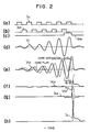
- Figs. 2(a) to (h) shown a plurality of signal waveforms generated at various parts of Fig. 1.
- Fig. 3 is a block diagram of the control circuit which is applicable to the pulse generators shown in Figs. 1, 4 and 5, respectively.
- Figs. 4 to 6 are circuit diagrams showing pulse generators for lasers according to another embodiments of the invention.
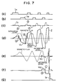
- Figs. 7(a) to (g) show a plurality of signal waveforms generated at various parts in the circuit of Fig. 6.
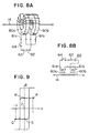
- Fig. 8A is a diagram showing an embodiment of the residual flux reset unit suited for use with the pulse generator according to the invention.
- Fig. 8B is a circuit diagram for the resetting unit of Fig. 8A.
- Fig. 9 is a diagram showing magnetic characteristics of the iron cores.
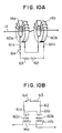
- Fig. 10A is a diagram showing another embodiment of the residual flux reset unit.
- Fig. 10B is a circuit diagram for the resetting unit of Fig. 10A.
- Fig. 11A is a diagram showing still another embodiment of the residual flux resetting unit.
- Fig. 11B is a circuit diagram for the resetting unit of Fig. 11A.
- the pulse generator designated generally with numeral 100, is connected to a laser device 102 from an LC resonant circuit 9 on the secondary side of a transformer 101 through a saturable reactor 103.
- a timing circuit 104 and a reset circuit 105 are arranged on the secondary side of the saturable reactor 103 and these circuits are also connected to a control circuit 106.
- One side of the control circuit 106 is connected to the bases B of transistors 3A and 3B which are connected to the primary winding of the transformer 101.
- the transformer 101 includes the primary winding 1 and the secondary winding 2.
- the ends of the primary winding 1 are respectively connected to the first and second transistors 3A and 3B forming switching elements.
- a lead line 4A brought out from the intermediate point of the primary winding 1 between the transistors 3A and 3B is connected to a dc power source 4.
- One end of the dc power source 4 is connected to the emitters E of the transistors 3A and 3B and a ground 5.
- the bases B of the transistors 3A and 3B are connected to the control circuit 106.
- a detecting winding 7, e.g., a current transformer, is connected to the control circuit 106 to detect the direction of current flow in the secondary winding 2.
- a capacitor 8 is connected in parallel between the ends of the secondary winding 2 to form an LC resonant circuit (tank circuit) 9.
- the LC resonant circuit 9 is connected to an output capacitor 11 and the laser device 102.
- the laser device 102 includes a discharge section 12 containing a laser gas and electrodes 12A and 12B, e.g., cathode and anode arranged within the discharge section 12.
- the ends of the electrodes 12A and 12B are connected in parallel with the output capacitor 11.
- the electrodes 12A and 12B and one end of the output capacitor 11 are connected to a ground 11E.
- the saturable reactor 103 is connected in series with one side of the electrodes 12A and 12B and the output capacitor 11 and the LC resonant circuit 9, respectively.
- the saturable reactor 103 includes an iron core, e.g., ring core 13 and a main winding 14 wound on the ring core 13, and the ends of the main winding 14 are respectively connected to the LC resonant circuit 9 and the output capacitor 11, etc.
- the timing circuit 104 and the reset circuit 105 are arranged on the secondary side (control windings) of the saturable reactor 103.
- the timing circuit 104 includes a control winding 15 wound on the core 13, a transistor 16 and a dc power source 17.
- the reset circuit 105 includes a pair of windings 20A and 20B which are wound on the core 13.
- a branch line 21 is brought out from between the windings 20A and 20B and connected to one end of a dc power source 22.
- the negative terminal of the dc power source 22 and one ends of the windings 20A and 20B are respectively connected to the emitters E and collectors C of transistors 23A and 23B.
- the emitters E are connected to a ground 24.
- the bases B of the transistors 16, 23A and 23B are connected to the control circuit 106.
- a current I s1 such as shown in (a) of Fig. 2 flows to the primary winding 1 from the dc power source 4.
- the abscissa represents the time t .
- the current I s1 induces a voltage in the secondary winding 2 electromagnetically coupled to the primary winding 1, thereby causing the flow of a current I c1 such as shown in (d) of Fig. 2.
- the capacitor 8 is connected in parallel with the secondary winding 2 to form the LC resonant circuit 9.
- the secondary current I s1 produces a secondary voltage V c1 as shown in (e) of Fig. 2.
- the detecting winding 7 detects the reversal of the current I c1 in the LC resonant circuit 9 to turn the first transistor 3A off and the second transistor 3B on through the control circuit 106.
- a current I s2 flows as shown in (b) of Fig. 2.
- the resulting voltage induced in the secondary winding 2 by the current I S2 is opposite in polarity to the induced voltage by the current I s1 .
- the current I c1 increases in magnitude each time it reverses.
- the main winding 14 of the saturable reactor 103 has a large inductance and thus a large impedance is presented to the oscillating voltage of the LC resonant circuit 9. As a result, practically no voltage appears across the capacitor 11.
- the magnetic flux within the core 13 is varied as shown by the dotted line in (e) of Fig. 2 in proportion to an time-integrated value of the voltage applied to the winding 14.
- the crossectional area of its core 13 and the number of turns of its winding 14 are preset to such values that the saturable reactor 103 is not saturated until the voltage V c1 of the LC resonant circuit 9 exceeds the desired value. As a result, the saturable reactor 103 is not saturated irrespective of time until the voltage of the LC resonant circuit 9 attains the core saturation level.
- the capacities of the first and second transistors 3A and 3B can be made small enough as compared with the case of the conventional method of supplying about one half of an electric energy to be supplied by every switching.
- the control circuit 106 detects that the voltage of the LC resonant circuit 9 has attained the desired value.
- the desired number of times of polarity reversal for the current in the secondary winding 2 of the transformer 101 has been preliminarily examined so that the detecting winding 7 detects each polarity reversal and the control circuit 106 counts the number of occurrences. when the count reaches the desired number of times of polarity reversal, the transistor 16 of the timing circuit 104 is turned on.
- Another method may be used in which the voltage V c1 is measured directly by a voltage divider to turn the transistor 16 on when the voltage V c1 reaches the desired value.
- the current flowing in the primary winding 1 opens and closes the transistors 3A and 3B so that the LC resonant circuit 9 causes LC resonance to store a large electric energy and this energy is controlled by the saturable reactor 103, thereby outputting a high voltage.
- the LC resonant circuit 9 causes LC resonance to store a large electric energy and this energy is controlled by the saturable reactor 103, thereby outputting a high voltage.
- the core 13 is saturated and the electric energy is transferred to the capacitor 11.
- the core 13 In order to transfer the maximum electric energy to the capacitor 11, the core 13 must be saturated at around the maximum voltage value of the capacitor 8.
- the transistor 16 connected to the control winding 15 is turned on to supply the current I ON from the dc power source 17.
- the main winding 14 and the control winding 15 from a transformer and thus the current I ON produces a current I c2 in the main winding 14, thereby charging the capacitor 11.
- This voltage is preset lower than the discharge initiating voltage of the laser device 102 and thus there is no danger of discharging the laser device 102.
- the voltage V c2 charged in the capacitor 11 by the current I ON charges a voltage of the opposite polarity to a voltage which is to be outputted finally.
- the voltage applied to the main winding 14 is decreased at a half wave (the A portion in (e) of Fig. 2) of the opposite polarity to the polarity of the voltage applied to the laser device 102 and thus the amount of change (the amount of decrease in this case) of the magnetic flux in the core is decreased.
- the voltage applied to the main winding 14 is increased and the amount of change of the flux in the core is increased, thereby saturating the core.
- the capacitor 11 is charged so that the resulting voltage produces a magnetic flux and this magnetic flux is utilized to saturate the core 13.
- the timing of saturating the core 13 can be adjusted in dependence on the magnitude of the voltage on the capacitor 11 or the magnitude of the current I ON flowing in the control winding 15.
- the timing circuit 104 by providing the timing circuit 104, the electric energy stored in the LC resonant circuit 9 can be outputted positively at the optimum time instant.
- the voltage V c1 of the LC resonant circuit 9 is a voltage which oscillates between positive and negative limits.
- the magnetic flux in the core 13 also oscillates between positive and negative saturation points.
- the initial value of the magnetic flux in the core 13 is reduced to substantially zero, the normal operation is performed.
- the initial value of the magnetic flux in the core 13 is dependent on the preceding discharge of the laser device 102 and it cannot always be near to zero.
- the residual voltage in the capacitor 11 varies due to variations in the discharge voltage and variations in the discharge time. As a result, variations are caused in the magnetic flux in the core 13 which is varied by the remaining voltage in the capacitor 11.
- the transistor 23A is turned on and the core 13 is saturated.
- the transistor 23A controls in such a manner that a sufficient time and current for saturating the core 13 in one direction are provided irrespective of the value of the magnetic flux in the core 13.
- the transistor 23A is turned off and the other transistor 23B is turned on, thereby energizing the core 13 in the reverse direction.
- the transistor 23B is turned off.
- the necessary current value, voltage value and applying time thereof for reducing the magnetic flux to zero has been determined preliminarily from the magnetic characteristic of the core 13.
- An induced voltage is charged in the capacitor 11 by the reset current from the control winding 20B.
- the charged voltage of the capacitor 11 also varies the magnetic flux in the core 13. Therefore, the on period of the transistor 23B for resetting the magnetic flux in the core 13 to zero is selected to have a value sufficient to reduce the total flux including the flux due to the capacitor 11.
- Figs. 8 to 11A there are illustrated another embodiments of the reset circuit in the pulse generator according to the invention.
- the resetting is effected by controlling the supply time of the reset current to the control winding.
- the present embodiment feature that the core of the saturable reactor is divided into a plurality of parts and also the single switching element is employed.
- by suitably selecting the crossectional area of each split core or by varying the number of turns of the main winding on the split cores it is possible to control the residual flux to not only zero but also any given value.
- two split cores which are saturable in different directions, it is possible to prevent the variation of any magnetic flux by the charged voltage of the output capacitor due to a reset current.
- FIG. 8A shows the reset circuit according to this embodiment.
- a saturable reactor includes an iron core splitted into two core 60a and 60b, a main winding 14 wound to extend over the split cores 60a and 60b, and control windings 61a and 61b which are respectively wound on the split cores 60a and 60b.
- a dc power source 62, a current controlling resistor 63 and a switch 64 are connected in series with the control windings 61a and 61b.
- Fig. 8B shows a circuit diagram of the reset circuit. When the switch 64 is closed, the directions of current flow in the control windings 61a and 61b are opposite to each other.
- a current i determined by the voltage of the dc power source 62 and the resistor 63 flows to the control windings 61a and 61b.
- the current i is preset to a current value sufficient for saturating the split cores 60a and 60b, respectively.
- Fig. 9 shows hysteresis curves (the solid lines) of the split cores 60a and 60b.
- the magnetic flux in the split core 60a is saturated to P and the magnetic flux in the split core 60b is saturated to Q.
- the switch 64 is opened so that the current i is reduced to zero, the residual flux in the split core 60a is reset to R and the residual flux in the split core 60b is reset to S.
- the characteristic of the cores on the whole with respect to the main winding 14 is one combining the characteristics of the split cores 60a and 60b and the corresponding hysteresis curve is shown by the dotted line in the Figure. Also, where the characteristics and crosssectional areas of the split cores 60a and 60b are the same, the residual flux becomes effectively Z or zero.
- control windings require only the single control circuit (the power source, switch, etc.). Also, the residual fluxes in the cores can be controlled partially and hence the residual fluxes can be easily reset to any given value.
- a saturable reactor includes main windings 14a and 14b which are provided separately for split cores 60a and 60b, respectively.
- the induced electromotive forces to the main windings 14a and 14b are proportional to the varying amounts of magnetic fluxes and the numbers of turns.
- Fig. 10B shows a circuit diagram for the reset circuit of Fig. 10A.
- Fig. 11A shows still another embodiment of the reset circuit according to the invention.
- a saturable reactor core is divided into three split cores 60a, 60b and 60c on which control windings 61a, 61b and 61c are respectively wound.
- a switch 65 for changing the direction of current flow is connected to the control winding 61c.
- the switch 65 By operating the switch 65, the direction of saturation of the split core 60c is reversed thereby varying the value to which the residual fluxes are reset.
- the resulting value of the residual flux can be easily varied by means of the switch 65 connected to the control winding 61c.
- Fig. 11B shows a circuit diagram of the reset circuit shown in Fig. 11A.
- the reset circuit of this embodiment can easily reset the residual fluxes in the cores to zero or any other value than the saturation region by use of the simple construction.
- switches 64 and 65 take the form of mechanical switches, it is needless to say that such switching elements as transistors may be used as in the circuit of Fig. 1.
- Fig. 3 is a block diagram showing an internal construction of the control circuit 106.
- a first timer is first brought into operation to generate a pulse signal.
- the pulse signal is amplified by a first driver circuit to turn the transistor 23A on.
- a second timer comes into operation with a delay so that a pulse signal is applied to a second driver circuit and the second drive circuit turns to transistor 23B on.
- a current flows to the control winding 20B and the magnetic flux in the core 13 is reset to zero.
- the magnetic flux including the effects of the voltages charged in the capacitors 8 and 11 by the induced voltage in the winding 14 is reset to zero.
- the residual flux in the core 13 is reset.
- a third timer comes into operation and a start signal generating circuit generates a pulse signal.
- This pulse signal is amplified by a fifth driver circuit to turn the transistor 3A on so that the capacitor 8 is charged by the current I s1 in the winding 1 and the resonant circuit 9 starts oscillating (the oscillation of voltage and current).
- the plarity reversals (oscillations) of the resonant circuit 9 are detected by the detecting winding 7 so that a pulse corresponding to each polarity is generated from an oscillation polarity detecting circuit and the transitors 3A and 3B are alternately turned on and off, thereby increasing the oscillating voltage and current of the resonant circuit 9.
- a fourth timer comes into operation and generates a pulse so that the transistor 16 is turned on and the saturable reactor 103 is saturated, thereby supplying the energy in the resonant circuit 9 to the capacitor 11.
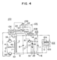
- the embodiment of Fig. 4 differs from the embodiment of Fig. 1 in that the capacitor 11 is charged directly from the dc power source 17 by means of the transistor 16.
- the transistor 16 and the dc power source 17 are protected from the high voltage by a surge absorving circuit 30 including resistors 26 and 29, a diode 28 and a capacitor 27.
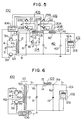
- FIG. 5 there is illustrated still another embodiment of the pulse generator according to the invention, which differs from the embodiment of Fig. 1 in that a magnetic pulse compression circuit 40 is provided between the saturable reactor 103 and the reset circuit 105 and the laser device 102.
- the magnetic pulse compression circuit 40 includes a saturable reactor 103 ⁇ and a capacitor 43 and it has the following functions and effects.
- the current I ON shown in (c) of Fig. 2 is supplied to the main winding 14 so that the capacitor 11 is charged by the current I ON and the sawtooth wave V c2 ⁇ shown in (f) of Fig. 2 is produced, thereby saturating the core 13.
- the voltage V c2 ⁇ is preset near to the discharge voltage so as to saturate the saturable reactor 103 in a short period of time, the danger of the laser device 102 being caused to malfunction due to the voltage V c2 ⁇ is conceivable.
- FIG. 6 there is illustrated still another embodiment of the pulse generator according to the invention which differs from the embodiment of Fig. 1 in that a core 50 is arranged between the primary and secondary windings 1 and 2 of the transformer 101.
- a resonant circuit is provided by utilizing the reversion of the voltage on the capacitor 8 due to the saturation of the core 50 of the transformer 101.
- a current I s1 flow to the primary winding 1 wound on the core 50 from the dc power source 4 as shown in (a) of Fig. 7. Since the primary and secondary windings 1 and 2 are magnetically coupled through the core 50 thus forming the transformer 101, the current I s1 causes the flow of a current I c1 in the secondary winding 2 as shown in (c) of Fig. 7. The current I c1 flows to the capacitor 8 thereby producing a voltage V c1 on the capacitor 8 as shown in (d) of Fig. 7. The voltage V c1 increases the magnetic flux in the core 50 to vary as shown by the dotted line in (d) of Fig. 7.
- the voltage V c1 is also applied to the winding 14 so that the magnetic flux in the core 13 is also increased to vary as shown in (e) of Fig. 7. Then, since the voltage-time products for transformer 101 and the saturable reactor 103 have been preset to become Z1 ⁇ Z2 as shown by equation (3), the core 50 is saturated first and the inductance of the secondary winding 2 is decreased. The charge in the capacitor 8 is discharge through the secondary winding 2 at a frequency determined by the descreased inductance and the capacitance of the capacitor 8 and a half cycle of the discharge current in (A in (c) of Fig. 7) flows. As a result, the polarity of the voltage on the capacitor 8 is reversed. When this occurs, the magnetic fluxes in the cores 13 and 50 begin to vary in the reverse direction.
- the discharge current I c1 or A of the capacitor 8 is detected by the detecting winding 7 so that the transistor 3A is turned off and the transistor 3B is turned on by the control circuit 106. Consequently, the capacitor 8 is charged in the opposite polarity to previously by the primary winding 1 and the dc power source 4 and its stored electric energy is increased.
- the capacitor 8 is again discharged and the polarity reversal of its voltage is caused. As a result, the on and off states of the transistors 3A and 3B are also reversed thereby charging the capacitor 8.
- the transistors 3A and 3B are turned on and off in accordance with the polarity of the voltage on the capacitor 8 so that the voltage on the capacitor 8 is increased and its electric energy is increased.
- the voltage waveform Z appearing on the capacitor 8 has a rectangular waveform and thus the electric energy of the output voltage is substantially constant even if the timing of saturating the saturable reactor 103 is varied more or less.
Landscapes
- Physics & Mathematics (AREA)
- Electromagnetism (AREA)
- Nonlinear Science (AREA)
- Engineering & Computer Science (AREA)
- Plasma & Fusion (AREA)
- Optics & Photonics (AREA)
- Lasers (AREA)
- Generation Of Surge Voltage And Current (AREA)
Claims (14)
- Générateur d'impulsions à haute tension (100) pour envoyer des impulsions à haute tension à un dispositif laser (102) comprenant
une source d'énergie à courant continu (4);
des moyens de commutation (3A,3B) pour appliquer et interrompre une tension à partir de ladite source d'énergie (4);
un transformateur (101) comprenant un enroulement primaire (1) et un enroulement secondaire (2), ledit enroulement primaire (1) étant raccordé auxdits moyens de commutation (3A,3B);
un circuit bouchon (9) comprenant ledit enroulement secondaire (2) dudit transformateur et un condensateur (8) raccordé aux deux extrémités dudit enroulement secondaire (2);
une réactance saturable (103) possédant un enroulement principal (14) raccordé audit circuit bouchon (9); et
des moyens (105) de suppression de flux magnétique pour appliquer un courant à des enroulements de commande (20A,20D) de ladite réactance saturable (103) pour éliminer pour l'essentiel un flux résiduel dans ladite réactance saturable (103),
caractérisé en ce que
lesdits moyens de commutation (3A,3B) appliquent et interrompent la tension délivrée par ladite source d'énergie (4) pendant une période d'oscillation dudit circuit bouchon (9), l'énergie électrique délivrée par ladite source d'énergie (4) étant stockée sous la forme d'oscillations électriques; et
un condensateur de sortie (11) est raccordé à la réactance saturable (103) en parallèle avec ledit dispositif laser (102), l'énergie électrique stockée dans ledit circuit bouchon (9) étant chargée sous la forme d'une énergie de charge et cette dernière étant déchargée en tant qu'impulsion appliquée audit dispositif laser (102), lorsque ledit enroulement principal (14) de ladite réactance saturable (103) est excité. - Générateur d'impulsions à haute tension selon la revendication 1, dans lequel lesdits moyens (105) de suppression de flux magnétique comprennent en outre une seconde source d'énergie à courant continu (22) et des seconds moyens de commutation (23A,23B) branchés entre ladite seconde source d'énergie (22) et lesdits enroulements de commande (20A,20B), lesdits seconds moyens de commutation (23A,23B) étant activés de telle sorte qu'un courant est envoyé par ladite seconde source d'énergie à courant continu (22) dans une direction desdits enroulements de commande (20A,20B) jusqu'à ce que ladite réactance saturable (103) soit saturée, et qu'un courant donné est envoyé dans l'autre direction desdits enroulements de commande (20A,20B) pour sensiblement réduire le flux magnétique résiduel dans ladite réactance saturable (103).
- Générateur d'impulsions à haute tension selon la revendication 2, dans lequel les enroulements de commande desdits moyens (105) de suppression de flux magnétique comprennent deux enroulements (20A,20B), dans lequel lesdits seconds moyens de commutation comprennent deux transistors (23A,23B), et dans lequel chacun desdits transistors (23A,23B) est branché en série avec lesdits enroulements de commande (20A,20B) et ladite seconde source d'énergie à courant continu (22) de sorte que les directions du flux de courant dans lesdits enroulements de commande (20A,20B) sont réciproquement opposés.
- Générateur d'impulsions à haute tension selon la revendication 3, dans laquelle ladite réactance saturable (103) comprend au moins deux noyaux fendus (60a,60b) couplés magnétiquement entre eux, et dans lequel lesdits moyens (105) de suppression de flux magnétique comprennent au moins deux enroulements de commande (61a,61b) dont chacun est enroulé sur l'un desdits noyaux fendus (60a,60b), et dans lequel un courant est envoyé à au moins l'un desdits enroulements de commande (61a,61b) pour saturer ledit noyau fendu (60a ou 60b) dans la direction opposée à celle de l'autre desdits enroulements de commande (61a,61b).
- Générateur d'impulsions à haute tension selon la revendication 4, dans lequel l'enroulement principal (14) de ladite réactance saturable (103) est enroulé avec un nombre prédéterminé de spires sur chacun desdits noyaux fendus (60a,60b).
- Générateur d'impulsions à haute tension selon la revendication 4, dans lequel un interrupteur (64) est raccordé à au moins l'un des enroulements de commande (61a,61b) de ladite réactance saturable (103) pour modifier de façon sélective le sens de circulation du courant dans cet enroulement de manière qu'il circule soit dans la même direction, soit dans la direction opposée à celle de circulation du courant dans l'autre desdits enroulements de commande (61a,61b).
- Générateur d'impulsions à haute tension selon la revendication 1, comportant en outre un circuit de commande de séquence de saturation (104) pour commander la séquence d'excitation de ladite réactance saturable (103).
- Générateur d'impulsions à haute tension selon la revendication 7, dans lequel ledit circuit de commande de séquence de saturation (104) comprend un autre enroulement de commande (15) prévu sur ladite réactance saturable (103), et des moyens de commande de courant (16,17,106) pour envoyer un courant audit autre enroulement de commande (15) pour saturer ladite réactance saturable (103).
- Générateur d'impulsions à haute tension selon la revendication 8, dans lequel lesdits moyens de commande de courant dudit circuit de commande de séquence de saturation (104) comprennent des moyens de comptage (106) pour compter le nombre d'inversions de la polarité de la tension aux bornes de l'enroulement secondaire (92) dudit transformateur (101), et un circuit générateur de courant (16,17), répondant au comptage d'un nombre prédéterminé d'inversions de polarité par lesdits moyens de comptage (106) pour envoyer audit autre enroulement de commande (15) un courant pour saturer ladite réactance saturable (103).
- Générateur d'impulsions à haute tension selon la revendication 7, dans lequel ledit circuit de commande de séquence de saturation (104) comprend des moyens de comptage (106) pour compter le nombre d'inversions de polarité aux bornes de l'enroulement secondaire (2) dudit transformateur (101), et un circuit de charge (15,16,17) répondant au comptage d'un nombre prédéterminé d'inversions de polarité par lesdits moyens de comptage (106) pour charger ledit condensateur de sortie (11) et de ce fait saturer ladite réactance saturable (103).
- Générateur d'impulsions à haute tension selon la revendication 1, dans lequel ledit transformateur (101) comprend un noyau de fer (15), et dans lequel la relation suivante est satisfaite
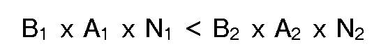
B₁ représentant une densité de flux de saturation dudit noyau de fer (50), A₁ une surface en coupe transversale dudit noyau de fer (50), N₁ le nombre de spires dans ledit second enroulement secondaire (2), B₂ une densité de flux de saturation du noyau (13) de ladite réactance saturable (103), A₂ une surface en coupe transversale dudit noyau (13) de la réactance, et N₂ le nombre de spires dudit enroulement principal (14). - Générateur d'impulsions à haute tension selon la revendication 1, comportant en outre une seconde réactance saturable (103') branchée en série entre ladite réactance saturable (103) et ladite charge (102) du type à décharge, et un second condensateur de sortie (43) branché en parallèle avec ladite charge (102) du type à décharge.
- Procédé pour générer des impulsions à haute tension pour envoyer lesdites impulsions à un dispositif laser (102), comprenant l'étape consistant à
appliquer et interrompre une tension d'alimentation d'une source d'énergie à courant continu (4) pour envoyer un courant à un enroulement primaire d'un transformateur (101), ledit transformateur possédant un enroulement secondaire (2), dont les deux extrémités sont raccordées à un condensateur (8), de manière à former un circuit bouchon (9),
caractérisé par les étapes suivantes :
envoi d'une énergie électrique de ladite tension d'alimentation appliquée et interrompue audit circuit bouchon (9) par l'intermédiaire dudit transformateur (101), ladite tension d'alimentation étant appliquée et interrompue en synchronisme avec une fréquence d'oscillation dudit circuit bouchon (9);
stockage de ladite énergie électrique envoyée audit circuit bouchon (9) sous la forme d'oscillations électriques;
charge d'un condensateur de sortie (11) branché en parallèle avec ledit dispositif laser (102), par commutation d'un noyau d'une réactance saturable(103) à la saturation lorsque la tension desdites oscillations dans ledit circuit bouchon (9) atteint une valeur prédéterminée,
le courant de charge partant dudit circuit bouchon (9) et traversant un enroulement principal (14) de ladite réactance saturable (103); et
décharge rapide de l'énergie stockée dans ledit condensateur de sortie (11) et dans ledit circuit bouchon (9) par déclenchement de la décharge desdits dispositifs laser (102) lorsque la tension appliquée audit condensateur de sortie (11) atteint la tension servant à déclencher la décharge dudit dispositif laser (102). - Procédé selon la revendication 13, selon lequel ledit procédé comprend en outre l'étape consistant à supprimer un flux résiduel dans ladite réactance saturable (103) au moyen de l'envoi d'un courant dans un enroulement de commande (20A,20B) de ladite réactance saturable (103).
Applications Claiming Priority (4)
| Application Number | Priority Date | Filing Date | Title |
|---|---|---|---|
| JP226029/86 | 1986-09-26 | ||
| JP22602986 | 1986-09-26 | ||
| JP71534/87 | 1987-03-27 | ||
| JP62071534A JPS63239808A (ja) | 1987-03-27 | 1987-03-27 | 鉄心リセツト装置 |
Publications (3)
| Publication Number | Publication Date |
|---|---|
| EP0261663A2 EP0261663A2 (fr) | 1988-03-30 |
| EP0261663A3 EP0261663A3 (en) | 1989-07-12 |
| EP0261663B1 true EP0261663B1 (fr) | 1992-06-17 |
Family
ID=26412631
Family Applications (1)
| Application Number | Title | Priority Date | Filing Date |
|---|---|---|---|
| EP19870113913 Expired - Lifetime EP0261663B1 (fr) | 1986-09-26 | 1987-09-23 | Dispositif à laser avec générateur d'impulsion haute-tension, générateur d'impulsion haute-tension et méthode de génération d'impulsion |
Country Status (6)
| Country | Link |
|---|---|
| US (1) | US4818892A (fr) |
| EP (1) | EP0261663B1 (fr) |
| KR (1) | KR920008042B1 (fr) |
| CN (1) | CN1011843B (fr) |
| CA (1) | CA1299233C (fr) |
| DE (1) | DE3779850T2 (fr) |
Cited By (1)
| Publication number | Priority date | Publication date | Assignee | Title |
|---|---|---|---|---|
| CN1326325C (zh) * | 2002-01-04 | 2007-07-11 | 斯勘的诺维亚系统公司 | 电力调制器 |
Families Citing this family (21)
| Publication number | Priority date | Publication date | Assignee | Title |
|---|---|---|---|---|
| NL9002153A (nl) * | 1990-10-04 | 1992-05-06 | Hollandse Signaalapparaten Bv | Laadinrichting. |
| US5567995A (en) * | 1994-10-20 | 1996-10-22 | The United States Of America As Represented By The Secretary Of The Air Force | Multi winding spiral generator |
| US5629844A (en) * | 1995-04-05 | 1997-05-13 | International Power Group, Inc. | High voltage power supply having multiple high voltage generators |
| JPH0926616A (ja) * | 1995-07-12 | 1997-01-28 | Fuji Photo Film Co Ltd | ストロボ充電回路 |
| US5650670A (en) * | 1995-07-27 | 1997-07-22 | The United States Of America As Represented By The Secretary Of The Air Force | Induction charge microwave pulse generator having a split ground plane |
| US5930125A (en) * | 1996-08-28 | 1999-07-27 | Siemens Medical Systems, Inc. | Compact solid state klystron power supply |
| JP3892589B2 (ja) * | 1998-07-14 | 2007-03-14 | 株式会社小松製作所 | 可飽和リアクトルおよびこれを用いたパルスレーザ用電源装置 |
| GB2344233B (en) * | 1998-11-30 | 2003-06-04 | Marconi Electronic Syst Ltd | Improvements in or relating to pulse line generators |
| US6831377B2 (en) * | 2000-05-03 | 2004-12-14 | University Of Southern California | Repetitive power pulse generator with fast rising pulse |
| US7151330B2 (en) * | 2003-03-20 | 2006-12-19 | Radiance Technologies, Inc. | Apparatus and method for generating high voltages using a voltage inversion generator and multiple closed-path ferrites |
| JP4587655B2 (ja) * | 2003-10-02 | 2010-11-24 | 東洋電機製造株式会社 | 分散電源用発電装置 |
| KR100702571B1 (ko) * | 2004-03-31 | 2007-04-04 | 국방과학연구소 | 레이저 거리 측정기의 레이저 출력회로 |
| RU2386207C2 (ru) * | 2008-01-31 | 2010-04-10 | Михаил Викторович Зубков | Коммутационный способ возбуждения параметрического резонанса электрических колебаний и устройство для его осуществления |
| RU2453022C2 (ru) * | 2010-06-17 | 2012-06-10 | Федеральное государственное унитарное предприятие "Научно-производственный центр газотурбостроения "Салют" (ФГУП "НПЦ газотурбостроения "Салют") | Устройство для одновременного питания электрофизических аппаратов высоким постоянным и частотно-импульсным напряжением субмикросекундного диапазона (варианты) |
| CN102611413B (zh) * | 2012-03-16 | 2014-08-20 | 浙江大学 | Igbt串联型高压脉冲发生器 |
| CN103856188B (zh) * | 2012-11-30 | 2017-03-01 | 深圳市海洋王照明工程有限公司 | 一种高压脉冲电路 |
| US20160118899A1 (en) * | 2014-10-24 | 2016-04-28 | Keithley Instruments, Inc. | Magnetization balancing method |
| JP7045250B2 (ja) * | 2018-04-20 | 2022-03-31 | 住友重機械工業株式会社 | レーザ装置およびその電源装置 |
| WO2019216793A1 (fr) * | 2018-05-07 | 2019-11-14 | Общество С Ограниченной Ответственностью Научно-Производственное Предприятие "Лучшие Технологии" | Dispositif d'alimentation haute tension d'appareils électro-physiques |
| CN109505583A (zh) * | 2018-12-27 | 2019-03-22 | 北京捷威思特科技有限公司 | 旋转脉冲器储能节 |
| CN113439371B (zh) * | 2019-03-26 | 2023-12-08 | 国立大学法人长冈技术科学大学 | 高电压脉冲产生装置、气体激光装置和电子器件的制造方法 |
Family Cites Families (12)
| Publication number | Priority date | Publication date | Assignee | Title |
|---|---|---|---|---|
| US2990539A (en) * | 1955-05-25 | 1961-06-27 | Ibm | Transistor amplifiers |
| US3211915A (en) * | 1960-04-05 | 1965-10-12 | Westinghouse Electric Corp | Semiconductor saturating reactor pulsers |
| JPS55124290A (en) * | 1979-03-20 | 1980-09-25 | Mitsubishi Electric Corp | Voiceless discharge type gas laser device |
| JPS57212512A (en) * | 1981-06-25 | 1982-12-27 | Toshiba Corp | Voltage resonance type high-frequency switching circuit |
| US4549091A (en) * | 1983-08-08 | 1985-10-22 | Standard Oil Company (Indiana) | Electrical excitation circuit for gas lasers |
| DE3335690C2 (de) * | 1983-09-30 | 1986-03-27 | Lambda Physik GmbH, 3400 Göttingen | Vorrichtung zum Erzeugen von Hochleistungs-Hochspannungsimpulsen hoher Wiederholfrequenz |
| US4595843A (en) * | 1984-05-07 | 1986-06-17 | Westinghouse Electric Corp. | Low core loss rotating flux transformer |
| US4707619A (en) * | 1985-02-13 | 1987-11-17 | Maxwell Laboratories, Inc. | Saturable inductor switch and pulse compression power supply employing the switch |
| US4684820A (en) * | 1985-02-13 | 1987-08-04 | Maxwell Laboratories, Inc. | Symmetrically charged pulse-forming circuit |
| EP0233903A1 (fr) * | 1985-09-02 | 1987-09-02 | Ascom Hasler AG | Element inductif commande electriquement |
| US4652771A (en) * | 1985-12-10 | 1987-03-24 | Westinghouse Electric Corp. | Oscillating flux transformer |
| US4694387A (en) * | 1987-01-08 | 1987-09-15 | Honeywell, Inc. | Inductive devices |
-
1987
- 1987-09-23 EP EP19870113913 patent/EP0261663B1/fr not_active Expired - Lifetime
- 1987-09-23 DE DE8787113913T patent/DE3779850T2/de not_active Expired - Lifetime
- 1987-09-24 CA CA 547785 patent/CA1299233C/fr not_active Expired - Lifetime
- 1987-09-25 US US07/101,171 patent/US4818892A/en not_active Expired - Fee Related
- 1987-09-25 KR KR1019870010632A patent/KR920008042B1/ko not_active Expired
- 1987-09-26 CN CN87106591A patent/CN1011843B/zh not_active Expired
Cited By (1)
| Publication number | Priority date | Publication date | Assignee | Title |
|---|---|---|---|---|
| CN1326325C (zh) * | 2002-01-04 | 2007-07-11 | 斯勘的诺维亚系统公司 | 电力调制器 |
Also Published As
| Publication number | Publication date |
|---|---|
| EP0261663A2 (fr) | 1988-03-30 |
| KR880004642A (ko) | 1988-06-07 |
| EP0261663A3 (en) | 1989-07-12 |
| DE3779850T2 (de) | 1992-12-24 |
| CA1299233C (fr) | 1992-04-21 |
| US4818892A (en) | 1989-04-04 |
| CN87106591A (zh) | 1988-04-06 |
| KR920008042B1 (ko) | 1992-09-21 |
| CN1011843B (zh) | 1991-02-27 |
| DE3779850D1 (de) | 1992-07-23 |
Similar Documents
| Publication | Publication Date | Title |
|---|---|---|
| EP0261663B1 (fr) | Dispositif à laser avec générateur d'impulsion haute-tension, générateur d'impulsion haute-tension et méthode de génération d'impulsion | |
| US5514918A (en) | Pulse generator | |
| EP0516397B1 (fr) | Laser à impulsion | |
| EP0329099B1 (fr) | Système d'allumage | |
| US3305794A (en) | Control rectifier inverter with resonant circuit and a choke | |
| US4662343A (en) | Method and apparatus for generating high voltage pulses | |
| US4812770A (en) | Saturable reactor current pulse generator | |
| EP0379991B1 (fr) | Circuit d'alimentation en puissance et méthode pour alimenter en puissance des lasers impulsionnels | |
| JPH0716055B2 (ja) | 高電圧パルス発生装置を備えるレーザ装置と高電圧パルス発生装置ならびにパルス発生方法 | |
| US4691272A (en) | Inverse rectifier | |
| RU2094646C1 (ru) | Высокочастотная электроразрядная система воспламенения | |
| EP0463705B1 (fr) | Dispositif pour excitation de la décharge d'un laser à gaz | |
| JPS62108588A (ja) | 充放電装置 | |
| JPH02148781A (ja) | パルスレーザ電源装置 | |
| RU2001506C1 (ru) | Преобразователь напр жени | |
| JP3268672B2 (ja) | インバータ駆動回路 | |
| WO1993000743A1 (fr) | Regulateur de phase a impulsions commandees | |
| RU2050682C1 (ru) | Устройство для заряда емкостного накопителя | |
| JPH11502965A (ja) | 補助電圧発生のための回路装置 | |
| JPH0276280A (ja) | パルスレーザ発振装置 | |
| RU2010467C1 (ru) | Магнитный формирователь импульсов | |
| SU1201977A1 (ru) | Импульсный преобразователь посто нного напр жени | |
| SU1190478A2 (ru) | Генератор пр моугольных импульсов | |
| SU1748233A1 (ru) | Генератор импульсов | |
| JP2611518B2 (ja) | パルスガスレーザ装置 |
Legal Events
| Date | Code | Title | Description |
|---|---|---|---|
| PUAI | Public reference made under article 153(3) epc to a published international application that has entered the european phase |
Free format text: ORIGINAL CODE: 0009012 |
|
| AK | Designated contracting states |
Kind code of ref document: A2 Designated state(s): DE FR GB NL SE |
|
| PUAL | Search report despatched |
Free format text: ORIGINAL CODE: 0009013 |
|
| AK | Designated contracting states |
Kind code of ref document: A3 Designated state(s): DE FR GB NL SE |
|
| 17P | Request for examination filed |
Effective date: 19890714 |
|
| 17Q | First examination report despatched |
Effective date: 19900625 |
|
| RBV | Designated contracting states (corrected) |
Designated state(s): DE FR GB |
|
| GRAA | (expected) grant |
Free format text: ORIGINAL CODE: 0009210 |
|
| AK | Designated contracting states |
Kind code of ref document: B1 Designated state(s): DE FR GB |
|
| REF | Corresponds to: |
Ref document number: 3779850 Country of ref document: DE Date of ref document: 19920723 |
|
| ET | Fr: translation filed | ||
| PLBE | No opposition filed within time limit |
Free format text: ORIGINAL CODE: 0009261 |
|
| STAA | Information on the status of an ep patent application or granted ep patent |
Free format text: STATUS: NO OPPOSITION FILED WITHIN TIME LIMIT |
|
| 26N | No opposition filed | ||
| PGFP | Annual fee paid to national office [announced via postgrant information from national office to epo] |
Ref country code: FR Payment date: 19930730 Year of fee payment: 7 |
|
| PGFP | Annual fee paid to national office [announced via postgrant information from national office to epo] |
Ref country code: GB Payment date: 19930913 Year of fee payment: 7 |
|
| PGFP | Annual fee paid to national office [announced via postgrant information from national office to epo] |
Ref country code: DE Payment date: 19931126 Year of fee payment: 7 |
|
| PG25 | Lapsed in a contracting state [announced via postgrant information from national office to epo] |
Ref country code: GB Effective date: 19940923 |
|
| GBPC | Gb: european patent ceased through non-payment of renewal fee |
Effective date: 19940923 |
|
| PG25 | Lapsed in a contracting state [announced via postgrant information from national office to epo] |
Ref country code: FR Effective date: 19950531 |
|
| PG25 | Lapsed in a contracting state [announced via postgrant information from national office to epo] |
Ref country code: DE Effective date: 19950601 |
|
| REG | Reference to a national code |
Ref country code: FR Ref legal event code: ST |