WO2020184644A1 - ワイヤ不着検査システム及びワイヤ不着検出装置並びにワイヤ不着検出方法 - Google Patents
ワイヤ不着検査システム及びワイヤ不着検出装置並びにワイヤ不着検出方法 Download PDFInfo
- Publication number
- WO2020184644A1 WO2020184644A1 PCT/JP2020/010693 JP2020010693W WO2020184644A1 WO 2020184644 A1 WO2020184644 A1 WO 2020184644A1 JP 2020010693 W JP2020010693 W JP 2020010693W WO 2020184644 A1 WO2020184644 A1 WO 2020184644A1
- Authority
- WO
- WIPO (PCT)
- Prior art keywords
- wire
- ultrasonic
- attachment
- difference
- display
- Prior art date
- Legal status (The legal status is an assumption and is not a legal conclusion. Google has not performed a legal analysis and makes no representation as to the accuracy of the status listed.)
- Ceased
Links
Images



Classifications
-
- G—PHYSICS
- G06—COMPUTING OR CALCULATING; COUNTING
- G06T—IMAGE DATA PROCESSING OR GENERATION, IN GENERAL
- G06T7/00—Image analysis
- G06T7/20—Analysis of motion
- G06T7/254—Analysis of motion involving subtraction of images
-
- G—PHYSICS
- G06—COMPUTING OR CALCULATING; COUNTING
- G06T—IMAGE DATA PROCESSING OR GENERATION, IN GENERAL
- G06T7/00—Image analysis
- G06T7/0002—Inspection of images, e.g. flaw detection
- G06T7/0004—Industrial image inspection
-
- G—PHYSICS
- G06—COMPUTING OR CALCULATING; COUNTING
- G06T—IMAGE DATA PROCESSING OR GENERATION, IN GENERAL
- G06T7/00—Image analysis
- G06T7/0002—Inspection of images, e.g. flaw detection
- G06T7/0004—Industrial image inspection
- G06T7/001—Industrial image inspection using an image reference approach
-
- H—ELECTRICITY
- H04—ELECTRIC COMMUNICATION TECHNIQUE
- H04N—PICTORIAL COMMUNICATION, e.g. TELEVISION
- H04N7/00—Television systems
- H04N7/18—Closed-circuit television [CCTV] systems, i.e. systems in which the video signal is not broadcast
- H04N7/183—Closed-circuit television [CCTV] systems, i.e. systems in which the video signal is not broadcast for receiving images from a single remote source
-
- H—ELECTRICITY
- H04—ELECTRIC COMMUNICATION TECHNIQUE
- H04R—LOUDSPEAKERS, MICROPHONES, GRAMOPHONE PICK-UPS OR LIKE ACOUSTIC ELECTROMECHANICAL TRANSDUCERS; ELECTRIC HEARING AIDS; PUBLIC ADDRESS SYSTEMS
- H04R1/00—Details of transducers, loudspeakers or microphones
- H04R1/02—Casings; Cabinets ; Supports therefor; Mountings therein
- H04R1/028—Casings; Cabinets ; Supports therefor; Mountings therein associated with devices performing functions other than acoustics, e.g. electric candles
-
- H—ELECTRICITY
- H10—SEMICONDUCTOR DEVICES; ELECTRIC SOLID-STATE DEVICES NOT OTHERWISE PROVIDED FOR
- H10W—GENERIC PACKAGES, INTERCONNECTIONS, CONNECTORS OR OTHER CONSTRUCTIONAL DETAILS OF DEVICES COVERED BY CLASS H10
- H10W72/00—Interconnections or connectors in packages
- H10W72/071—Connecting or disconnecting
- H10W72/0711—Apparatus therefor
-
- H—ELECTRICITY
- H10—SEMICONDUCTOR DEVICES; ELECTRIC SOLID-STATE DEVICES NOT OTHERWISE PROVIDED FOR
- H10W—GENERIC PACKAGES, INTERCONNECTIONS, CONNECTORS OR OTHER CONSTRUCTIONAL DETAILS OF DEVICES COVERED BY CLASS H10
- H10W72/00—Interconnections or connectors in packages
- H10W72/071—Connecting or disconnecting
- H10W72/075—Connecting or disconnecting of bond wires
-
- H—ELECTRICITY
- H10—SEMICONDUCTOR DEVICES; ELECTRIC SOLID-STATE DEVICES NOT OTHERWISE PROVIDED FOR
- H10W—GENERIC PACKAGES, INTERCONNECTIONS, CONNECTORS OR OTHER CONSTRUCTIONAL DETAILS OF DEVICES COVERED BY CLASS H10
- H10W72/00—Interconnections or connectors in packages
- H10W72/50—Bond wires
-
- H—ELECTRICITY
- H10—SEMICONDUCTOR DEVICES; ELECTRIC SOLID-STATE DEVICES NOT OTHERWISE PROVIDED FOR
- H10W—GENERIC PACKAGES, INTERCONNECTIONS, CONNECTORS OR OTHER CONSTRUCTIONAL DETAILS OF DEVICES COVERED BY CLASS H10
- H10W72/00—Interconnections or connectors in packages
- H10W72/90—Bond pads, in general
-
- H—ELECTRICITY
- H10—SEMICONDUCTOR DEVICES; ELECTRIC SOLID-STATE DEVICES NOT OTHERWISE PROVIDED FOR
- H10W—GENERIC PACKAGES, INTERCONNECTIONS, CONNECTORS OR OTHER CONSTRUCTIONAL DETAILS OF DEVICES COVERED BY CLASS H10
- H10W90/00—Package configurations
-
- G—PHYSICS
- G06—COMPUTING OR CALCULATING; COUNTING
- G06T—IMAGE DATA PROCESSING OR GENERATION, IN GENERAL
- G06T2207/00—Indexing scheme for image analysis or image enhancement
- G06T2207/10—Image acquisition modality
- G06T2207/10016—Video; Image sequence
-
- G—PHYSICS
- G06—COMPUTING OR CALCULATING; COUNTING
- G06T—IMAGE DATA PROCESSING OR GENERATION, IN GENERAL
- G06T2207/00—Indexing scheme for image analysis or image enhancement
- G06T2207/30—Subject of image; Context of image processing
- G06T2207/30108—Industrial image inspection
- G06T2207/30148—Semiconductor; IC; Wafer
-
- G—PHYSICS
- G06—COMPUTING OR CALCULATING; COUNTING
- G06T—IMAGE DATA PROCESSING OR GENERATION, IN GENERAL
- G06T2207/00—Indexing scheme for image analysis or image enhancement
- G06T2207/30—Subject of image; Context of image processing
- G06T2207/30108—Industrial image inspection
- G06T2207/30152—Solder
-
- H—ELECTRICITY
- H10—SEMICONDUCTOR DEVICES; ELECTRIC SOLID-STATE DEVICES NOT OTHERWISE PROVIDED FOR
- H10W—GENERIC PACKAGES, INTERCONNECTIONS, CONNECTORS OR OTHER CONSTRUCTIONAL DETAILS OF DEVICES COVERED BY CLASS H10
- H10W72/00—Interconnections or connectors in packages
- H10W72/071—Connecting or disconnecting
- H10W72/0711—Apparatus therefor
- H10W72/07183—Means for monitoring
-
- H—ELECTRICITY
- H10—SEMICONDUCTOR DEVICES; ELECTRIC SOLID-STATE DEVICES NOT OTHERWISE PROVIDED FOR
- H10W—GENERIC PACKAGES, INTERCONNECTIONS, CONNECTORS OR OTHER CONSTRUCTIONAL DETAILS OF DEVICES COVERED BY CLASS H10
- H10W72/00—Interconnections or connectors in packages
- H10W72/071—Connecting or disconnecting
- H10W72/075—Connecting or disconnecting of bond wires
- H10W72/07531—Techniques
-
- H—ELECTRICITY
- H10—SEMICONDUCTOR DEVICES; ELECTRIC SOLID-STATE DEVICES NOT OTHERWISE PROVIDED FOR
- H10W—GENERIC PACKAGES, INTERCONNECTIONS, CONNECTORS OR OTHER CONSTRUCTIONAL DETAILS OF DEVICES COVERED BY CLASS H10
- H10W72/00—Interconnections or connectors in packages
- H10W72/50—Bond wires
- H10W72/541—Dispositions of bond wires
- H10W72/5449—Dispositions of bond wires not being orthogonal to a side surface of the chip, e.g. fan-out arrangements
-
- H—ELECTRICITY
- H10—SEMICONDUCTOR DEVICES; ELECTRIC SOLID-STATE DEVICES NOT OTHERWISE PROVIDED FOR
- H10W—GENERIC PACKAGES, INTERCONNECTIONS, CONNECTORS OR OTHER CONSTRUCTIONAL DETAILS OF DEVICES COVERED BY CLASS H10
- H10W72/00—Interconnections or connectors in packages
- H10W72/50—Bond wires
- H10W72/59—Bond pads specially adapted therefor
-
- H—ELECTRICITY
- H10—SEMICONDUCTOR DEVICES; ELECTRIC SOLID-STATE DEVICES NOT OTHERWISE PROVIDED FOR
- H10W—GENERIC PACKAGES, INTERCONNECTIONS, CONNECTORS OR OTHER CONSTRUCTIONAL DETAILS OF DEVICES COVERED BY CLASS H10
- H10W72/00—Interconnections or connectors in packages
- H10W72/90—Bond pads, in general
- H10W72/931—Shapes of bond pads
- H10W72/932—Plan-view shape, i.e. in top view
-
- H—ELECTRICITY
- H10—SEMICONDUCTOR DEVICES; ELECTRIC SOLID-STATE DEVICES NOT OTHERWISE PROVIDED FOR
- H10W—GENERIC PACKAGES, INTERCONNECTIONS, CONNECTORS OR OTHER CONSTRUCTIONAL DETAILS OF DEVICES COVERED BY CLASS H10
- H10W72/00—Interconnections or connectors in packages
- H10W72/90—Bond pads, in general
- H10W72/941—Dispositions of bond pads
- H10W72/944—Dispositions of multiple bond pads
- H10W72/9445—Top-view layouts, e.g. mirror arrays
-
- H—ELECTRICITY
- H10—SEMICONDUCTOR DEVICES; ELECTRIC SOLID-STATE DEVICES NOT OTHERWISE PROVIDED FOR
- H10W—GENERIC PACKAGES, INTERCONNECTIONS, CONNECTORS OR OTHER CONSTRUCTIONAL DETAILS OF DEVICES COVERED BY CLASS H10
- H10W90/00—Package configurations
- H10W90/20—Configurations of stacked chips
- H10W90/24—Configurations of stacked chips at least one of the stacked chips being laterally offset from a neighbouring stacked chip, e.g. chip stacks having a staircase shape
-
- H—ELECTRICITY
- H10—SEMICONDUCTOR DEVICES; ELECTRIC SOLID-STATE DEVICES NOT OTHERWISE PROVIDED FOR
- H10W—GENERIC PACKAGES, INTERCONNECTIONS, CONNECTORS OR OTHER CONSTRUCTIONAL DETAILS OF DEVICES COVERED BY CLASS H10
- H10W90/00—Package configurations
- H10W90/20—Configurations of stacked chips
- H10W90/28—Configurations of stacked chips the stacked chips having different sizes, e.g. chip stacks having a pyramidal shape
-
- H—ELECTRICITY
- H10—SEMICONDUCTOR DEVICES; ELECTRIC SOLID-STATE DEVICES NOT OTHERWISE PROVIDED FOR
- H10W—GENERIC PACKAGES, INTERCONNECTIONS, CONNECTORS OR OTHER CONSTRUCTIONAL DETAILS OF DEVICES COVERED BY CLASS H10
- H10W90/00—Package configurations
- H10W90/701—Package configurations characterised by the relative positions of pads or connectors relative to package parts
- H10W90/751—Package configurations characterised by the relative positions of pads or connectors relative to package parts of bond wires
- H10W90/752—Package configurations characterised by the relative positions of pads or connectors relative to package parts of bond wires between stacked chips
-
- H—ELECTRICITY
- H10—SEMICONDUCTOR DEVICES; ELECTRIC SOLID-STATE DEVICES NOT OTHERWISE PROVIDED FOR
- H10W—GENERIC PACKAGES, INTERCONNECTIONS, CONNECTORS OR OTHER CONSTRUCTIONAL DETAILS OF DEVICES COVERED BY CLASS H10
- H10W90/00—Package configurations
- H10W90/701—Package configurations characterised by the relative positions of pads or connectors relative to package parts
- H10W90/751—Package configurations characterised by the relative positions of pads or connectors relative to package parts of bond wires
- H10W90/754—Package configurations characterised by the relative positions of pads or connectors relative to package parts of bond wires between a chip and a stacked insulating package substrate, interposer or RDL
Definitions
- the present invention relates to a wire non-attachment inspection system for detecting non-attachment of a wire connecting an electrode of a semiconductor element mounted on a substrate and an electrode of a substrate, a wire non-attachment detection device, and a wire non-attachment detection method.
- wire bonding devices are used to connect the electrodes of the substrate and the electrodes of the semiconductor chip with wires.
- a wire bonding apparatus a method of detecting non-adhesion between an electrode of a semiconductor chip and a wire by an electric means of passing a current between the wire and the semiconductor chip is used (see, for example, Patent Document 1). ..
- an object of the present invention is to provide a wire non-delivery inspection system capable of detecting wire non-delivery with high accuracy in a short time.
- the wire non-attachment inspection system of the present invention is a wire that connects a substrate, a semiconductor element attached to the substrate, an electrode of the semiconductor element and an electrode of the substrate, or one electrode of the semiconductor element and another electrode of the semiconductor element.
- This is a wire non-attachment inspection system for semiconductor devices, which includes an ultrasonic oscillator, an ultrasonic vibrator connected to the ultrasonic oscillator, and ultrasonically vibrates the semiconductor device by the electric power from the ultrasonic oscillator, and a semiconductor. It is equipped with a camera that captures the moving image of the device, a display that displays the moving image captured by the camera, and a control unit that adjusts the ultrasonic oscillator and analyzes the moving image captured by the camera.
- the feature is that the difference between the images of one frame and the previous frame before that is calculated, and the image display of the wire whose difference exceeds a predetermined threshold is displayed on the display differently from the image display of the other wires. And.
- the amplitude of the non-attached wire becomes larger than the amplitude of the normally connected wire. Therefore, the difference between the images of one frame of the captured moving image and the previous frame before that is calculated, and the image display of the wire whose image difference exceeds a predetermined threshold, that is, the non-arrival wire is displayed as an image of another wire.
- the image of the non-attached wire can be displayed on the display in a distinctive manner from other images. As a result, the inspector can detect the non-arrival wire by displaying the image on the display.
- the difference between the amplitude of the non-attached wire and the amplitude of the normally connected wire is remarkable, it is possible to detect the non-attachment of the wire with high accuracy.
- the camera acquires images of all the wires contained in the semiconductor device, analyzes them at the same time, and displays them on the display, it is possible to inspect all the wires in a short time even if the number of wires increases. ..
- the control unit displays the image display of the excess region in which the difference in the vibration region of the wire exceeds a predetermined threshold value on the display different from the image display of the other region. Good.
- the image display of a certain area By making the image display of a certain area different in this way, the area or area where the different image is displayed becomes large, and the inspector can easily detect the non-arrival wire.
- control unit may calculate the difference by changing the number of frames between one frame for calculating the difference and the previous frame, or the frame rate of the moving image.
- control unit may change the oscillation frequency of the ultrasonic oscillator to ultrasonically excite the semiconductor device with the ultrasonic exciter.
- the natural frequency of the wire changes depending on the length of the wire between the bond points and the diameter of the wire. Therefore, by changing the oscillation frequency of the ultrasonic oscillator and ultrasonically exciting the semiconductor device with an ultrasonic vibrator, non-attachment inspection of a plurality of wires having different bond point lengths or wire diameters can be performed. Can be done at once. As a result, non-attachment inspection of wires having different lengths or diameters can be performed in a short time.
- the ultrasonic vibrator may be an ultrasonic vibrator connected to a substrate of a semiconductor device to ultrasonically vibrate the substrate.
- the ultrasonic exciter may be an ultrasonic speaker arranged around the semiconductor device.
- the wire can be directly ultrasonically vibrated, and non-attachment detection of the wire can be performed with higher accuracy.
- the wire non-attachment detection device of the present invention is a wire that connects a substrate, a semiconductor element attached to the substrate, an electrode of the semiconductor element and an electrode of the substrate, or one electrode of the semiconductor element and another electrode of the semiconductor element.
- a wire non-attachment detection device for a semiconductor device including, an ultrasonic oscillator, an ultrasonic vibrator connected to the ultrasonic oscillator and ultrasonically vibrating the semiconductor device with power from the ultrasonic oscillator, and a semiconductor. It includes a camera that captures the moving image of the device and a control unit that adjusts the ultrasonic oscillator and analyzes the moving image captured by the camera.
- the control unit includes one frame of the captured moving image and a previous frame before that. It is characterized in that the difference between the images is calculated and a non-delivery detection signal is output when the difference exceeds a predetermined threshold value.
- the amplitude of the non-attached wire becomes larger than the amplitude of the normally connected wire. Therefore, the difference between the images of one frame of the captured moving image and the previous frame before that can be calculated, and the non-attachment of the wire can be detected when the difference between the images exceeds a predetermined threshold value. Since the difference between the amplitude of the non-attached wire and the amplitude of the normally connected wire is remarkable, it is possible to detect the non-attachment of the wire with high accuracy.
- the camera can acquire images of all the wires contained in the semiconductor device and analyze the difference between the images at the same time, it is possible to detect the non-delivery of the wires of the entire semiconductor device in a short time even if the number of wires increases. it can.
- control unit may calculate the difference by changing the number of frames between one frame for calculating the difference and the previous frame, or the frame rate of the moving image.
- the vibration frequency of the wire and the timing of the frame of the moving image for calculating the difference can be adjusted to remarkably detect the difference, and the accuracy of non-delivery detection can be improved.
- control unit may change the oscillation frequency of the ultrasonic oscillator to ultrasonically vibrate the semiconductor device with the ultrasonic exciter.
- the ultrasonic vibrator may be an ultrasonic vibrator connected to the substrate of the semiconductor device to ultrasonically vibrate the substrate, or an ultrasonic speaker arranged around the semiconductor device. May be.
- the wire can be directly ultrasonically vibrated, and the non-attachment detection of the wire can be performed with higher accuracy.
- the wire non-attachment detection method of the present invention is a wire that connects a substrate, a semiconductor element attached to the substrate, an electrode of the semiconductor element and an electrode of the substrate, or one electrode of the semiconductor element and another electrode of the semiconductor element.
- This is a method for detecting wire non-attachment of a semiconductor device, which comprises an ultrasonic oscillator, an ultrasonic vibrator connected to the ultrasonic oscillator, and ultrasonically vibrating the semiconductor device by power from the ultrasonic oscillator, and a semiconductor.
- the preparation step includes preparing a display for displaying a moving image captured by a camera and connecting the display to a control unit, and displaying an image of a wire whose difference exceeds a predetermined threshold.
- the non-delivery detection step may detect non-delivery of the wire based on the image displayed on the display, including a display step of displaying on the display differently from the image display of the other wire.
- the image display of the excess region in which the difference in the vibration region of the wire exceeds a predetermined threshold value may be displayed on the display different from the image display of the other region.
- the present invention can provide a wire non-delivery inspection system capable of detecting wire non-delivery with high accuracy in a short time.
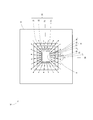
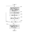
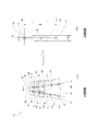
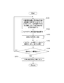
- FIG. 1 It is a system diagram which shows the structure of the wire non-attachment inspection system of embodiment. It is a top view which shows the image which the camera took. It is a flowchart which shows the operation of the control part of the wire non-attachment inspection system shown in FIG. (A) is an enlarged plan view of part A of FIG. 3 when the substrate is ultrasonically vibrated, and (b) is an enlarged plan view of part B shown in (a). It is a top view which shows the excess area when the substrate is ultrasonically vibrated. It is a system diagram which shows the structure of the wire non-attachment inspection system of another embodiment. It is a system diagram which shows the structure of the wire non-delivery detection apparatus of embodiment. It is a flowchart which shows the operation of the wire non-delivery detection apparatus shown in FIG.
- the wire non-delivery inspection system 100 of the embodiment performs a non-attachment inspection between the wire 30 of the semiconductor device 10 and the electrode 12 of the substrate 11 or the electrodes 25 to 28 of the semiconductor device 10.
- the wire non-attachment inspection system 100 includes an ultrasonic oscillator 40, an ultrasonic vibrator 42 which is an ultrasonic vibrator, a camera 45, a display 48, and a control unit 50.
- the semiconductor device 10 to be inspected by the wire non-attachment inspection system 100 is mounted by stacking semiconductor chips 21 to 24 in four stages on the substrate 11, and the electrodes 25 to 28 and the substrate 11 of the semiconductor chips 21 to 24.
- the electrodes 12 of the above are continuously connected by one wire 30.
- the semiconductor chips 21 to 24 constitute the semiconductor element 20.
- One wire 30 includes a first-stage wire 31 that connects the electrode 25 of the first-stage semiconductor chip 21 and the electrode 12 of the substrate 11, and electrodes 26 to each of the second-stage to fourth-stage semiconductor chips 22 to 24. It is composed of second-stage to fourth-stage wires 32 to 34 connecting 28 and electrodes 25 to 27 of the semiconductor chips 21 to 23 of the first to third stages, respectively.
- the ultrasonic oscillator 40 outputs AC power having a frequency in the ultrasonic region and causes the ultrasonic vibrator 42 to vibrate ultrasonically.
- the ultrasonic vibrator 42 is a member that is driven by AC power in the frequency region of ultrasonic waves input from the ultrasonic oscillator 40 and vibrates ultrasonically.
- it may be composed of a piezo element or the like.
- the ultrasonic vibrator 42 is connected to the substrate 11 of the semiconductor device 10.
- the camera 45 is arranged on the upper side of the semiconductor device 10, and as shown in FIG. 2, the substrate 11 and the semiconductor chips 21 to 24 attached to the substrate 11 and the outer periphery of the semiconductor chips 21 to 24 are arranged. Images of the electrodes 25 to 28 arranged in the unit, the electrodes 12 of the substrate 11 arranged around the first-stage semiconductor chip 21, and the wires 30 for continuously connecting the electrodes 12 and 25 to 28. To do.
- the camera 45 captures an image of a moving image and outputs it to the control unit 50.
- the display 48 is an image display device that displays a moving image captured by the camera 45.
- the control unit 50 is a computer including a CPU and a storage unit inside.
- the ultrasonic oscillator 40 is connected to the control unit 50 and operates according to a command from the control unit 50. Further, the control unit 50 adjusts the camera 45, analyzes the moving image captured by the camera 45, and outputs the result to the display 48.
- the control unit 50 outputs a command to the ultrasonic oscillator 40 to output AC power having a frequency in the ultrasonic region.
- the ultrasonic oscillator 40 outputs AC power having a predetermined frequency, for example, a frequency of about 40 kHz.
- the AC power output by the ultrasonic oscillator 40 is input to the ultrasonic vibrator 42, and the ultrasonic vibrator 42 vibrates ultrasonically.
- the ultrasonic vibrator 42 vibrates the substrate 11 of the semiconductor device 10 with ultrasonic vibration, whereby each wire 30 of the semiconductor device 10 is ultrasonically vibrated.
- the wire 30a shown in FIG. 4A is normally connected to the electrodes 12, 25 to 28.
- the first-stage to fourth-stage wires 31a to 34a are connected to the electrodes 12, 25 to 27 to which the lower ends of the first-stage to fourth-stage wires 31a to 34a are connected, respectively. It vibrates laterally at a natural frequency f0 between each of the electrodes 25 to 28 to which the upper end is connected.
- the natural frequency f0 differs depending on the diameter of the wire 30 and the distance a between the electrodes 25 and 26 and the electrodes 26 and 27, but in a general semiconductor device 10, it is often on the order of several tens of Hz.
- the non-attached wire 30b is in a non-attached state with the electrode 26 of the second-stage semiconductor chip 22. Therefore, when the non-attached wire 30b is ultrasonically vibrated, the second-stage wire 32b and the third-stage wire 33b are the electrodes 27 of the first-stage semiconductor chip 21 and the third-stage semiconductor chip 23. It vibrates laterally at the natural frequency f1 between and.
- the distance between the electrode 25 and the electrode 27 is 2a, which is twice the distance a between the electrodes 25, 26 and the electrodes 26, 27.
- the natural frequency f1 of the second-stage wire 32b and the third-stage wire 33b of 30b is about 1 ⁇ 2 of f0, and in a general semiconductor device 10, it is often on the order of 20 to 30 Hz.
- the substrate 11 and the semiconductor chips 21 to 24 do not have a portion that vibrates naturally even when ultrasonically vibrated, low-frequency natural vibrations such as the wire 30a and the non-attached wire 30b do not occur.
- the control unit 50 captures a moving image of the semiconductor device 10 ultrasonically vibrated in this way with the camera 45, and as shown in step S103 of FIG. 3, the captured image. Is stored in the storage unit.
- the normally connected first-stage to fourth-stage wires 31a to 34a of the wires 30a vibrate in the lateral direction at a natural frequency of several tens of Hz.
- the frame rate of the moving image is 24 to 60 frames per second. Therefore, for example, the images of the first-stage to fourth-stage wires 31a to 34a of one frame become like the alternate long and short dash line on the left side of the center line 39a of the wire 30a in FIG. 4 (a).
- the image of the front frame is like the alternate long and short dash line on the right side of the center line 39a of the wire 30a in FIG. 4A.
- the control unit 50 reads out the image data of the moving image stored in the storage unit, and as shown in step S104 of FIG. 3, the first-stage to fourth-stage wires of one frame shown in FIG. 4A.
- the images of 31a to 34a are compared with the images of the first to fourth stage wires 31a to 34a of the previous previous frame, and the difference ⁇ da between them is calculated.
- this difference ⁇ da is small in the normal wire 30a.
- the difference ⁇ da is an amount proportional to the amplitude of the first-stage to fourth-stage wires 31a to 34a.
- the second-stage wire 32b and the third-stage wire 33b of the non-attached wire 30b which are in a non-attached state with the electrode 26 of the second-stage semiconductor chip 22, vibrate significantly in the lateral direction at 20 to 30 Hz. ..
- the frame rate of the moving image is 24 to 60 frames per second, for example, the images of the second-stage wire 32b and the third-stage wire 33b of one frame are shown in FIG. 4 (a).
- (b) are like the alternate long and short dash line on the left side of the center line 39a of the non-attached wire 30b, and the image of the previous previous frame is the center line of the non-attached wire 30b in FIGS. It looks like the alternate long and short dash line on the right side of 39b.
- the control unit 50 has an image of the second-stage wire 32b and the third-stage wire 33b of one frame and the second stage of the previous front frame as shown in FIG. 4B.
- the difference ⁇ db between the image of the eye wire 32b and the image of the third stage wire 33b is calculated.
- the difference ⁇ db between the second-stage wire 32b and the third-stage wire 33b of the non-attached wire 30b is very large and exceeds a predetermined threshold value ⁇ S.
- the difference ⁇ db is an amount proportional to the amplitude of the second-stage wire 32b and the third-stage wire 33b.
- the control unit 50 has an image of the second-stage wire 32b and the third-stage wire 33b of one frame, and the second-stage wire 32b and the third-stage wire of the previous previous frame.
- a predetermined threshold ⁇ S it is determined as YES in step S105 of FIG. 3, and the process proceeds to step S106 of FIG. 3, and the images of the second-stage wire 32b and the third-stage wire 33b
- the display on the display 48 of the above is different from the image of the first to fourth stage wires 31a to 34a of the normally connected wires 30a.
- the images of the second-stage wire 32b and the third-stage wire 33b of the non-attached wire 30b are displayed in red or displayed in bright white, and the substrate 11 and each semiconductor chip are displayed. It is displayed so as to be distinguishable from the images of 21 to 24 or the images of the first to fourth stage wires 31a to 34a of the normally connected wires 30a.
- the non-attached wire 30b is displayed in red, so that the presence or absence of the non-attached wire 30b and its position can be detected at a glance.
- control unit 50 determines NO in step S105 of FIG. 3, the control unit 50 returns to step S101 of FIG. 3 and continues ultrasonic vibration of the semiconductor device 10 and imaging of a moving image.
- the control unit 50 has an image of the second-stage wire 32b and the third-stage wire 33b of one frame, and the second-stage wire 32b and the third-stage wire 33b of the previous previous frame.
- the difference ⁇ db from the image exceeds the predetermined threshold value ⁇ S
- the difference ⁇ db in the vibration region of the second-stage wire 32b and the third-stage wire 33b shown by hatching in FIG. 5 exceeds the predetermined threshold value ⁇ S.
- the image display of the excess areas 35 and 36 may be displayed on the display 48 differently from the image display of the other areas.
- the area wider than the images of the second-stage wire 32b and the third-stage wire 33b of the non-arrival wire 30b is displayed in red, so that the inspector can more easily non-arrival.
- the wire 30b can be detected.
- the control unit 50 calculates an image difference ⁇ d between one frame of the captured moving image and the previous previous frame, and displays another image of the non-arrival wire 30b in which the image difference ⁇ d exceeds a predetermined threshold ⁇ S.
- the image of the non-arrival wire 30b can be displayed on the display 48 in a distinctive manner from other images. This allows the inspector to detect the non-attached wire 30b from the image on the display 48. Since the difference between the amplitude of the non-attached wire 30b and the amplitude of the normally connected wire 30a is remarkable, the non-attachment detection of the non-attached wire 30b can be performed with high accuracy. Further, since the camera 45 can acquire images of all the wires 30 included in the semiconductor device 10 and simultaneously analyze and display them on the display 48, all the wires 30 can be obtained in a short time even if the number of wires 30 increases. Non-delivery inspection can be performed.
- the natural frequency f0 between the electrodes 12 and 25 to 28 of the normal wire 30a is on the order of several tens of Hz
- the electrodes 25 of the second-stage wire 32b and the third-stage wire 33b of the non-attached wire 30b is on the order of 20 to 30 Hz
- the frame rate of the moving image is 24 to 60 frames per second
- the difference ⁇ d between the image of one frame and the previous previous frame is set.
- the difference ⁇ d between the image of one frame and the image of the previous frame or the image of the previous frame is calculated. It may be compared with the threshold value ⁇ S. This corresponds to capturing a moving image at a rate of 1/2 or 1/3 of the frame rate. Further, the frame rate of the moving image may be changed according to the natural frequencies of the normal wire 30a and the non-arrival wire 30b, and set to a frame rate at which the difference ⁇ d becomes remarkable. In this way, the control unit 50 may calculate the difference ⁇ d by changing the number of frames between one frame and the previous frame or the frame rate of the moving image. As a result, the difference ⁇ d can be remarkably detected by adjusting the timing of the frame of the moving image for calculating the difference ⁇ d with the natural frequencies f0 and f1 of the normal wire 30a and the non-arrival wire 30b.
- control unit 50 may change the frequency of the AC power of the ultrasonic oscillator 40 to ultrasonically vibrate the semiconductor device 10.
- the natural frequency of the wire 30 varies depending on the length of the wire 30 between the bond points and the wire diameter.
- the semiconductor device 10 is ultrasonically vibrated by changing the oscillation frequency of the AC power of the ultrasonic oscillator 40. , Non-delivery detection of each part of each wire 30 can be effectively performed.
- the change in the oscillation frequency of the AC power of the ultrasonic oscillator 40 can be freely selected, but for example, the frequency may be swept from 10 kHz to 150 kHz so as to increase the frequency, or conversely, a high frequency to a low frequency. May be swept towards.
- the inspector detects the non-attached wire 30b by displaying the image display of the non-attached wire 30b on the display 48 differently from other image displays.
- the control unit 50 may determine that there is an image of the non-arrival wire 30b in which the difference ⁇ d exceeds a predetermined threshold value ⁇ S, and in that case, display the non-arrival detection of the wire 30 on the display 48. .. In this case, for example, a word such as "non-arrival wire detection" may be displayed on the display 48.
- the ultrasonic oscillator 40, the ultrasonic vibrator 42, the camera 45, and the display 48 are arranged, and the ultrasonic oscillator 42 is superposed. Connecting to the ultrasonic oscillator 40 and connecting the ultrasonic oscillator 40, the camera 45, and the display 48 to the control unit 50 to configure the wire non-attachment inspection system 100 constitutes a preparatory step. Then, controlling the ultrasonic oscillator 40 by the control unit 50 and ultrasonically vibrating the substrate 11 with the ultrasonic vibrator 42 constitutes an ultrasonic vibration step.
- control unit 50 captures a moving image of the semiconductor device 10 and calculates the difference ⁇ d of the images between the frames of the captured moving image, which constitutes an imaging step and a difference calculation step, respectively. Further, displaying the image of the non-arrival wire 30b whose difference ⁇ d exceeds the predetermined threshold value ⁇ S on the display 48 differently from the image of the normal wire 30a constitutes a display step. Then, the inspector detecting the non-delivery wire 30b based on the image of the display 48 constitutes the non-delivery detection step.
- the wire non-attachment inspection system 200 has an ultrasonic speaker 43 in which the ultrasonic vibrator 42 of the wire non-attachment inspection system 100 described with reference to FIGS. 1 to 5 is arranged around the semiconductor device 10. It is a substitute for.
- the wire non-attachment inspection system 200 can directly ultrasonically vibrate the wire 30 in addition to the same actions and effects as the wire non-attachment inspection system 100 described above, and can detect the non-attachment of the wire 30 with higher accuracy. be able to.
- the wire non-attachment detection device 300 of the embodiment will be described with reference to FIG. 7.
- the same parts as those of the wire non-attachment inspection system 100 of the embodiment described above with reference to FIGS. 1 to 5 are designated by the same reference numerals, and the description thereof will be omitted.
- the wire non-delivery detection device 300 of the embodiment does not include the display 48, and the control unit 50 determines the difference ⁇ d between the image of one frame of the moving image captured by the camera 45 and the previous frame before that. Is calculated, and when the difference ⁇ d exceeds a predetermined threshold value ⁇ S, a non-delivery detection signal is output to the outside.
- the control unit 50 outputs the AC power in the ultrasonic region of the frequency from the ultrasonic oscillator 40 to ultrasonically vibrate the ultrasonic vibrator 42 to vibrate the substrate of the semiconductor device 10.
- 11 is ultrasonically vibrated, a moving image of the semiconductor device 10 is imaged by the camera 45, the image data of the moving image is stored in the storage unit, and the difference ⁇ d of the images is calculated.
- control unit 50 determines YES in step S105 of FIG. 8, the control unit 50 proceeds to step S201 of FIG. 8 and outputs a non-delivery detection signal to the outside.
- the non-delivery detection signal from the control unit 50 is input to various external devices.
- the external device is a display device or a warning lamp
- the wording "wire non-delivery detection" may be displayed or the warning lamp may be turned on.
- the semiconductor device 10 may be removed from the subsequent production line as a defective product.
- control unit 50 may calculate the number and position of the non-arrival wire 30b from the result of analyzing the image and include the information on the number and position of the non-arrival wire 30b in the non-arrival signal.
- the ultrasonic oscillator 40, the ultrasonic vibrator 42, and the camera 45 are arranged, and the ultrasonic oscillator 42 is used as the ultrasonic oscillator 40.
- Connecting the ultrasonic oscillator 40 and the camera 45 to the control unit 50 constitutes a preparatory step.
- controlling the ultrasonic oscillator 40 by the control unit 50 and ultrasonically vibrating the substrate 11 with the ultrasonic vibrator 42 constitutes an ultrasonic vibration step.
- control unit 50 captures a moving image of the semiconductor device 10 and calculates the difference ⁇ d of the images between the frames of the captured moving image, which constitutes an imaging step and a difference calculation step, respectively. Then, outputting a non-delivery detection signal when the difference ⁇ d exceeds a predetermined threshold value ⁇ S constitutes a non-delivery detection step.
- the semiconductor device 10 to be inspected is mounted on the substrate 11 with the semiconductor chips 21 to 24 laminated in four stages, and the electrodes 25 to 24 of the semiconductor chips 21 to 24 are mounted.
- the present invention is not limited to this.
- it can be applied to a non-attachment inspection of the wire 30 of the semiconductor device 10 in which one semiconductor chip 21 is mounted on the substrate 11 and the semiconductor chip 21 and the electrode 12 of the substrate 11 are connected by the wire 30.
Landscapes
- Engineering & Computer Science (AREA)
- Physics & Mathematics (AREA)
- Computer Vision & Pattern Recognition (AREA)
- General Physics & Mathematics (AREA)
- Theoretical Computer Science (AREA)
- Quality & Reliability (AREA)
- Multimedia (AREA)
- Signal Processing (AREA)
- Acoustics & Sound (AREA)
- Investigating Or Analyzing Materials By The Use Of Ultrasonic Waves (AREA)
- Wire Bonding (AREA)
- Testing Or Measuring Of Semiconductors Or The Like (AREA)
Abstract
Description
Claims (14)
- 基板と、
前記基板に取付けられた半導体素子と、
前記半導体素子の電極と前記基板の電極、又は、前記半導体素子の一の電極と前記半導体素子の他の電極とを接続するワイヤと、を備える半導体装置のワイヤ不着検査システムであって、
超音波発振器と、
前記超音波発振器に接続されて前記超音波発振器からの電力により前記半導体装置を超音波加振する超音波加振器と、
前記半導体装置の動画を撮像するカメラと、
前記カメラで撮像した動画を表示するディスプレイと、
前記超音波発振器を調整すると共に、前記カメラで撮像した動画を解析する制御部と、を備え、
前記制御部は、撮像した動画の1つのフレームとそれ以前の前フレームとの画像の差分を算出し、
前記差分が所定の閾値を超えた前記ワイヤの画像表示を他の前記ワイヤの画像表示と異ならせて前記ディスプレイに表示すること、
を特徴とするワイヤ不着検査システム。 - 請求項1に記載のワイヤ不着検査システムであって、
前記制御部は、
前記ワイヤの振動領域の内の前記差分が所定の前記閾値を超えた超過領域の画像表示を他の領域の画像表示と異ならせて前記ディスプレイに表示すること、
を特徴とするワイヤ不着検査システム。 - 請求項1又は2に記載のワイヤ不着検査システムであって、
前記制御部は、
前記差分を算出する1つのフレームと前フレームとの間のフレーム数、或いは、動画のフレームレートを変化させて前記差分を算出すること、
を特徴とするワイヤ不着検査システム。 - 請求項1又は2に記載のワイヤ不着検査システムであって、
前記制御部は、
前記超音波発振器の発振周波数を変化させて前記超音波加振器で前記半導体装置を超音波加振すること、
を特徴とするワイヤ不着検査システム。 - 請求項1又は2に記載のワイヤ不着検査システムであって、
前記超音波加振器は、前記半導体装置の前記基板に接続されて前記基板を超音波振動させる超音波振動子であること、
を特徴とするワイヤ不着検査システム。 - 請求項1又は2に記載のワイヤ不着検査システムであって、
前記超音波加振器は、前記半導体装置の周囲に配置された超音波スピーカーであること、
を特徴とするワイヤ不着検査システム。 - 基板と、
前記基板に取付けられた半導体素子と、
前記半導体素子の電極と前記基板の電極、又は、前記半導体素子の一の電極と前記半導体素子の他の電極とを接続するワイヤと、を備える半導体装置のワイヤ不着検出装置であって、
超音波発振器と、
前記超音波発振器に接続されて前記超音波発振器からの電力により前記半導体装置を超音波加振する超音波加振器と、
前記半導体装置の動画を撮像するカメラと、
前記超音波発振器を調整すると共に、前記カメラで撮像した動画を解析する制御部と、を備え、
前記制御部は、撮像した動画の1つのフレームとそれ以前の前フレームとの画像の差分を算出し、
前記差分が所定の閾値を超えた場合に不着検出信号を出力すること、
を特徴とするワイヤ不着検出装置。 - 請求項7に記載のワイヤ不着検出装置であって、
前記制御部は、
前記差分を算出する1つのフレームと前フレームとの間のフレーム数、或いは、動画のフレームレートを変化させて前記差分を算出すること、
を特徴とするワイヤ不着検出装置。 - 請求項7又は8に記載のワイヤ不着検出装置であって、
前記制御部は、
前記超音波発振器の発振周波数を変化させて前記超音波加振器で前記半導体装置を超音波加振すること、
を特徴とするワイヤ不着検出装置。 - 請求項7又は8に記載のワイヤ不着検出装置であって、
前記超音波加振器は、前記半導体装置の前記基板に接続されて前記基板を超音波振動させる超音波振動子であること、
を特徴とするワイヤ不着検出装置。 - 請求項7又は8に記載のワイヤ不着検出装置であって、
前記超音波加振器は、前記半導体装置の周囲に配置された超音波スピーカーであること、
を特徴とするワイヤ不着検出装置。 - 基板と、前記基板に取付けられた半導体素子と、前記半導体素子の電極と前記基板の電極、又は、前記半導体素子の一の電極と前記半導体素子の他の電極とを接続するワイヤと、を備える半導体装置のワイヤ不着検出方法であって、
超音波発振器と、前記超音波発振器に接続されて前記超音波発振器からの電力により前記半導体装置を超音波加振する超音波加振器と、前記半導体装置の動画を撮像するカメラと、前記超音波発振器と前記カメラとが接続される制御部と、を準備する準備ステップと、
前記超音波発振器からの電力によって前記超音波加振器で前記基板を超音波加振する超音波加振ステップと、
超音波加振された前記半導体装置の動画を前記カメラで撮像する撮像ステップと、
撮像した動画の1つのフレームとそれ以前の前フレームとの画像の差分を算出する差分算出ステップと、
前記差分が所定の閾値を超えた場合にワイヤの不着を検出する不着検出ステップと、
を含むことを特徴とするワイヤ不着検出方法。 - 請求項12に記載のワイヤ不着検出方法であって、
前記準備ステップは、前記カメラで撮像した動画を表示するディスプレイを準備し、前記ディスプレイを前記制御部に接続することを含み、
前記差分が所定の閾値を超えた前記ワイヤの画像表示を他の前記ワイヤの画像表示と異ならせて前記ディスプレイに表示する表示ステップを含み、
前記不着検出ステップは、前記ディスプレイに表示された画像に基づいて前記ワイヤの不着を検出すること、
を特徴とするワイヤ不着検出方法。 - 請求項13に記載のワイヤ不着検出方法であって、
前記表示ステップは、
前記ワイヤの振動領域の内の前記差分が所定の前記閾値を超えた超過領域の画像表示を他の領域の画像表示と異ならせて前記ディスプレイに表示すること、
を特徴とするワイヤ不着検出方法。
Priority Applications (5)
| Application Number | Priority Date | Filing Date | Title |
|---|---|---|---|
| JP2021505118A JP7019231B2 (ja) | 2019-03-13 | 2020-03-12 | ワイヤ不着検査システム及びワイヤ不着検出装置並びにワイヤ不着検出方法 |
| SG11202104391RA SG11202104391RA (en) | 2019-03-13 | 2020-03-12 | Wire non-attachment inspection system, wire non-attachment detection device, and wire non-attachment detection method |
| US17/428,963 US20220130026A1 (en) | 2019-03-13 | 2020-03-12 | Wire non-attachment inspection system, wire non-attachment detection device, and wire non-attachment detection method |
| KR1020217001424A KR102413267B1 (ko) | 2019-03-13 | 2020-03-12 | 와이어 불착 검사 시스템, 와이어 불착 검출 장치 및 와이어 불착 검출 방법 |
| CN202080005972.3A CN112997307B (zh) | 2019-03-13 | 2020-03-12 | 打线失败检查系统、检测装置以及检测方法 |
Applications Claiming Priority (2)
| Application Number | Priority Date | Filing Date | Title |
|---|---|---|---|
| JP2019-046296 | 2019-03-13 | ||
| JP2019046296 | 2019-03-13 |
Publications (1)
| Publication Number | Publication Date |
|---|---|
| WO2020184644A1 true WO2020184644A1 (ja) | 2020-09-17 |
Family
ID=72426656
Family Applications (1)
| Application Number | Title | Priority Date | Filing Date |
|---|---|---|---|
| PCT/JP2020/010693 Ceased WO2020184644A1 (ja) | 2019-03-13 | 2020-03-12 | ワイヤ不着検査システム及びワイヤ不着検出装置並びにワイヤ不着検出方法 |
Country Status (7)
| Country | Link |
|---|---|
| US (1) | US20220130026A1 (ja) |
| JP (1) | JP7019231B2 (ja) |
| KR (1) | KR102413267B1 (ja) |
| CN (1) | CN112997307B (ja) |
| SG (1) | SG11202104391RA (ja) |
| TW (1) | TWI760708B (ja) |
| WO (1) | WO2020184644A1 (ja) |
Cited By (1)
| Publication number | Priority date | Publication date | Assignee | Title |
|---|---|---|---|---|
| JPWO2022239067A1 (ja) * | 2021-05-10 | 2022-11-17 |
Citations (6)
| Publication number | Priority date | Publication date | Assignee | Title |
|---|---|---|---|---|
| JPH09181140A (ja) * | 1995-12-26 | 1997-07-11 | Toshiba Microelectron Corp | 半導体集積回路組立検査装置及び検査方法 |
| JP2008084881A (ja) * | 2006-09-25 | 2008-04-10 | Toshiba Corp | 電子装置の製造方法およびその検査方法 |
| JP2009071051A (ja) * | 2007-09-13 | 2009-04-02 | Toyota Motor Corp | ボンディングワイヤ検査装置およびボンディングワイヤ検査方法 |
| WO2014171160A1 (ja) * | 2013-04-15 | 2014-10-23 | 株式会社新川 | 半導体装置および半導体装置の製造方法 |
| JP2017022310A (ja) * | 2015-07-14 | 2017-01-26 | 三菱電機株式会社 | 半導体装置、半導体装置の劣化評価方法、半導体装置を含むシステム |
| JP2019100951A (ja) * | 2017-12-06 | 2019-06-24 | 新電元工業株式会社 | 半導体装置の検査方法、及び検査装置 |
Family Cites Families (11)
| Publication number | Priority date | Publication date | Assignee | Title |
|---|---|---|---|---|
| US5532739A (en) * | 1993-10-06 | 1996-07-02 | Cognex Corporation | Automated optical inspection apparatus |
| JPH09213752A (ja) | 1996-01-31 | 1997-08-15 | Kaijo Corp | ワイヤボンディング装置における不着検出回路 |
| JP2000137026A (ja) * | 1998-10-30 | 2000-05-16 | Suzuki Motor Corp | 異常検査方法およびワイヤボンディング装置の接合良否検査システム |
| TWI282133B (en) * | 2005-12-23 | 2007-06-01 | Advanced Semiconductor Eng | Method of wire bonding the chip with a plurality of solder pads |
| JP4275724B1 (ja) * | 2008-07-16 | 2009-06-10 | 株式会社新川 | ボンディング良否判定方法およびボンディング良否判定装置ならびにボンディング装置 |
| JP2010056106A (ja) | 2008-08-26 | 2010-03-11 | Nec Electronics Corp | ワイヤボンディング装置、これを用いたワイヤボンディング方法 |
| JP4625858B2 (ja) * | 2008-09-10 | 2011-02-02 | 株式会社カイジョー | ワイヤボンディング方法、ワイヤボンディング装置及びワイヤボンディング制御プログラム |
| JP2015114242A (ja) * | 2013-12-12 | 2015-06-22 | 株式会社新川 | ワイヤボンディングの検査方法及びワイヤボンディングの検査装置 |
| TWI562252B (en) * | 2014-02-17 | 2016-12-11 | Shinkawa Kk | Detecting discharging device, wire bonding device and detecting discharging method |
| JP5950994B2 (ja) * | 2014-12-26 | 2016-07-13 | 株式会社新川 | 実装装置 |
| WO2018110417A1 (ja) * | 2016-12-14 | 2018-06-21 | 株式会社新川 | ワイヤボンディング装置及びワイヤボンディング方法 |
-
2020
- 2020-03-12 JP JP2021505118A patent/JP7019231B2/ja active Active
- 2020-03-12 WO PCT/JP2020/010693 patent/WO2020184644A1/ja not_active Ceased
- 2020-03-12 SG SG11202104391RA patent/SG11202104391RA/en unknown
- 2020-03-12 CN CN202080005972.3A patent/CN112997307B/zh active Active
- 2020-03-12 US US17/428,963 patent/US20220130026A1/en not_active Abandoned
- 2020-03-12 TW TW109108246A patent/TWI760708B/zh active
- 2020-03-12 KR KR1020217001424A patent/KR102413267B1/ko not_active Expired - Fee Related
Patent Citations (6)
| Publication number | Priority date | Publication date | Assignee | Title |
|---|---|---|---|---|
| JPH09181140A (ja) * | 1995-12-26 | 1997-07-11 | Toshiba Microelectron Corp | 半導体集積回路組立検査装置及び検査方法 |
| JP2008084881A (ja) * | 2006-09-25 | 2008-04-10 | Toshiba Corp | 電子装置の製造方法およびその検査方法 |
| JP2009071051A (ja) * | 2007-09-13 | 2009-04-02 | Toyota Motor Corp | ボンディングワイヤ検査装置およびボンディングワイヤ検査方法 |
| WO2014171160A1 (ja) * | 2013-04-15 | 2014-10-23 | 株式会社新川 | 半導体装置および半導体装置の製造方法 |
| JP2017022310A (ja) * | 2015-07-14 | 2017-01-26 | 三菱電機株式会社 | 半導体装置、半導体装置の劣化評価方法、半導体装置を含むシステム |
| JP2019100951A (ja) * | 2017-12-06 | 2019-06-24 | 新電元工業株式会社 | 半導体装置の検査方法、及び検査装置 |
Cited By (2)
| Publication number | Priority date | Publication date | Assignee | Title |
|---|---|---|---|---|
| JPWO2022239067A1 (ja) * | 2021-05-10 | 2022-11-17 | ||
| JP7340302B2 (ja) | 2021-05-10 | 2023-09-07 | ヤマハロボティクスホールディングス株式会社 | 不良検出装置及び不良検出方法 |
Also Published As
| Publication number | Publication date |
|---|---|
| CN112997307B (zh) | 2024-06-18 |
| TW202103292A (zh) | 2021-01-16 |
| TWI760708B (zh) | 2022-04-11 |
| SG11202104391RA (en) | 2021-05-28 |
| KR20210021057A (ko) | 2021-02-24 |
| KR102413267B1 (ko) | 2022-06-27 |
| US20220130026A1 (en) | 2022-04-28 |
| CN112997307A (zh) | 2021-06-18 |
| JP7019231B2 (ja) | 2022-02-15 |
| JPWO2020184644A1 (ja) | 2021-06-03 |
Similar Documents
| Publication | Publication Date | Title |
|---|---|---|
| JP5987510B2 (ja) | 光走査装置及び光走査制御装置 | |
| JP4752952B2 (ja) | 力学量センサ、及び該力学量センサの製造方法 | |
| CN107615133B (zh) | 光扫描装置 | |
| US20110155789A1 (en) | Bonding apparatus | |
| CN104216112B (zh) | 光扫描装置、光扫描控制装置以及光扫描单元 | |
| JPWO2009028152A1 (ja) | 圧電アクチュエータおよびこれを用いた光学反射素子および圧電駆動装置 | |
| JP7019231B2 (ja) | ワイヤ不着検査システム及びワイヤ不着検出装置並びにワイヤ不着検出方法 | |
| JP7432263B2 (ja) | 超音波加振式不良検出装置及びワイヤ不良検出システム | |
| JP2010041638A (ja) | マイクロホン装置の検査装置 | |
| TWI823376B (zh) | 不良檢測裝置及不良檢測方法 | |
| JPH112643A (ja) | 加速度センサの周波数特性検査装置 | |
| JP4343996B1 (ja) | ワイヤボンディング装置及びキャピラリの振幅測定方法 | |
| TWI802991B (zh) | 超音波振動式不良檢測裝置及線材不良檢測系統 | |
| JPWO2022091247A5 (ja) | ||
| WO2021246271A1 (ja) | 音響式不良検出装置及び不良検出方法 | |
| US12583186B2 (en) | Ultrasonic bonding method, ultrasonic bonding apparatus, and ultrasonic bonding system | |
| JP2016206048A (ja) | 物理量センサー用回路、物理量センサー、及び物理量センサーの製造方法 | |
| JP5356148B2 (ja) | プローバー装置及び検査方法 | |
| TWI334031B (en) | Testing system and testing method for display apparatus | |
| JPH1164003A (ja) | 角速度センサ | |
| JP2010048598A (ja) | 微小構造体の検査装置および微小構造体の検査方法 | |
| JP2015200580A (ja) | 角速度検出回路、角速度センサ、電子機器および角速度検出回路の調整方法 | |
| JP2001041970A (ja) | 加速度センサおよび該加速度センサの製造方法 | |
| JPH05209780A (ja) | 周波数解析装置 | |
| WO2018012214A1 (ja) | 半導体センサチップ、半導体センサチップアレイ、および超音波診断装置 |
Legal Events
| Date | Code | Title | Description |
|---|---|---|---|
| 121 | Ep: the epo has been informed by wipo that ep was designated in this application |
Ref document number: 20770532 Country of ref document: EP Kind code of ref document: A1 |
|
| ENP | Entry into the national phase |
Ref document number: 2021505118 Country of ref document: JP Kind code of ref document: A |
|
| ENP | Entry into the national phase |
Ref document number: 20217001424 Country of ref document: KR Kind code of ref document: A |
|
| NENP | Non-entry into the national phase |
Ref country code: DE |
|
| 122 | Ep: pct application non-entry in european phase |
Ref document number: 20770532 Country of ref document: EP Kind code of ref document: A1 |