WO2020184213A1 - 光検出器 - Google Patents
光検出器 Download PDFInfo
- Publication number
- WO2020184213A1 WO2020184213A1 PCT/JP2020/008228 JP2020008228W WO2020184213A1 WO 2020184213 A1 WO2020184213 A1 WO 2020184213A1 JP 2020008228 W JP2020008228 W JP 2020008228W WO 2020184213 A1 WO2020184213 A1 WO 2020184213A1
- Authority
- WO
- WIPO (PCT)
- Prior art keywords
- region
- semiconductor substrate
- insulating
- conductive type
- photodetector according
- Prior art date
- Legal status (The legal status is an assumption and is not a legal conclusion. Google has not performed a legal analysis and makes no representation as to the accuracy of the status listed.)
- Ceased
Links
Images







Classifications
-
- H—ELECTRICITY
- H10—SEMICONDUCTOR DEVICES; ELECTRIC SOLID-STATE DEVICES NOT OTHERWISE PROVIDED FOR
- H10F—INORGANIC SEMICONDUCTOR DEVICES SENSITIVE TO INFRARED RADIATION, LIGHT, ELECTROMAGNETIC RADIATION OF SHORTER WAVELENGTH OR CORPUSCULAR RADIATION
- H10F77/00—Constructional details of devices covered by this subclass
- H10F77/20—Electrodes
- H10F77/206—Electrodes for devices having potential barriers
-
- H—ELECTRICITY
- H10—SEMICONDUCTOR DEVICES; ELECTRIC SOLID-STATE DEVICES NOT OTHERWISE PROVIDED FOR
- H10F—INORGANIC SEMICONDUCTOR DEVICES SENSITIVE TO INFRARED RADIATION, LIGHT, ELECTROMAGNETIC RADIATION OF SHORTER WAVELENGTH OR CORPUSCULAR RADIATION
- H10F30/00—Individual radiation-sensitive semiconductor devices in which radiation controls the flow of current through the devices, e.g. photodetectors
- H10F30/20—Individual radiation-sensitive semiconductor devices in which radiation controls the flow of current through the devices, e.g. photodetectors the devices having potential barriers, e.g. phototransistors
- H10F30/21—Individual radiation-sensitive semiconductor devices in which radiation controls the flow of current through the devices, e.g. photodetectors the devices having potential barriers, e.g. phototransistors the devices being sensitive to infrared, visible or ultraviolet radiation
- H10F30/22—Individual radiation-sensitive semiconductor devices in which radiation controls the flow of current through the devices, e.g. photodetectors the devices having potential barriers, e.g. phototransistors the devices being sensitive to infrared, visible or ultraviolet radiation the devices having only one potential barrier, e.g. photodiodes
- H10F30/225—Individual radiation-sensitive semiconductor devices in which radiation controls the flow of current through the devices, e.g. photodetectors the devices having potential barriers, e.g. phototransistors the devices being sensitive to infrared, visible or ultraviolet radiation the devices having only one potential barrier, e.g. photodiodes the potential barrier working in avalanche mode, e.g. avalanche photodiodes
-
- H—ELECTRICITY
- H10—SEMICONDUCTOR DEVICES; ELECTRIC SOLID-STATE DEVICES NOT OTHERWISE PROVIDED FOR
- H10F—INORGANIC SEMICONDUCTOR DEVICES SENSITIVE TO INFRARED RADIATION, LIGHT, ELECTROMAGNETIC RADIATION OF SHORTER WAVELENGTH OR CORPUSCULAR RADIATION
- H10F39/00—Integrated devices, or assemblies of multiple devices, comprising at least one element covered by group H10F30/00, e.g. radiation detectors comprising photodiode arrays
- H10F39/80—Constructional details of image sensors
- H10F39/803—Pixels having integrated switching, control, storage or amplification elements
- H10F39/8033—Photosensitive area
-
- H—ELECTRICITY
- H10—SEMICONDUCTOR DEVICES; ELECTRIC SOLID-STATE DEVICES NOT OTHERWISE PROVIDED FOR
- H10F—INORGANIC SEMICONDUCTOR DEVICES SENSITIVE TO INFRARED RADIATION, LIGHT, ELECTROMAGNETIC RADIATION OF SHORTER WAVELENGTH OR CORPUSCULAR RADIATION
- H10F39/00—Integrated devices, or assemblies of multiple devices, comprising at least one element covered by group H10F30/00, e.g. radiation detectors comprising photodiode arrays
- H10F39/80—Constructional details of image sensors
- H10F39/807—Pixel isolation structures
-
- H—ELECTRICITY
- H10—SEMICONDUCTOR DEVICES; ELECTRIC SOLID-STATE DEVICES NOT OTHERWISE PROVIDED FOR
- H10F—INORGANIC SEMICONDUCTOR DEVICES SENSITIVE TO INFRARED RADIATION, LIGHT, ELECTROMAGNETIC RADIATION OF SHORTER WAVELENGTH OR CORPUSCULAR RADIATION
- H10F77/00—Constructional details of devices covered by this subclass
- H10F77/10—Semiconductor bodies
- H10F77/14—Shape of semiconductor bodies; Shapes, relative sizes or dispositions of semiconductor regions within semiconductor bodies
- H10F77/147—Shapes of bodies
-
- H—ELECTRICITY
- H10—SEMICONDUCTOR DEVICES; ELECTRIC SOLID-STATE DEVICES NOT OTHERWISE PROVIDED FOR
- H10F—INORGANIC SEMICONDUCTOR DEVICES SENSITIVE TO INFRARED RADIATION, LIGHT, ELECTROMAGNETIC RADIATION OF SHORTER WAVELENGTH OR CORPUSCULAR RADIATION
- H10F77/00—Constructional details of devices covered by this subclass
- H10F77/10—Semiconductor bodies
- H10F77/14—Shape of semiconductor bodies; Shapes, relative sizes or dispositions of semiconductor regions within semiconductor bodies
- H10F77/148—Shapes of potential barriers
-
- H—ELECTRICITY
- H10—SEMICONDUCTOR DEVICES; ELECTRIC SOLID-STATE DEVICES NOT OTHERWISE PROVIDED FOR
- H10F—INORGANIC SEMICONDUCTOR DEVICES SENSITIVE TO INFRARED RADIATION, LIGHT, ELECTROMAGNETIC RADIATION OF SHORTER WAVELENGTH OR CORPUSCULAR RADIATION
- H10F77/00—Constructional details of devices covered by this subclass
- H10F77/20—Electrodes
- H10F77/206—Electrodes for devices having potential barriers
- H10F77/241—Electrodes for devices having potential barriers comprising ring electrodes
-
- H—ELECTRICITY
- H10—SEMICONDUCTOR DEVICES; ELECTRIC SOLID-STATE DEVICES NOT OTHERWISE PROVIDED FOR
- H10F—INORGANIC SEMICONDUCTOR DEVICES SENSITIVE TO INFRARED RADIATION, LIGHT, ELECTROMAGNETIC RADIATION OF SHORTER WAVELENGTH OR CORPUSCULAR RADIATION
- H10F77/00—Constructional details of devices covered by this subclass
- H10F77/40—Optical elements or arrangements
- H10F77/413—Optical elements or arrangements directly associated or integrated with the devices, e.g. back reflectors
-
- H—ELECTRICITY
- H10—SEMICONDUCTOR DEVICES; ELECTRIC SOLID-STATE DEVICES NOT OTHERWISE PROVIDED FOR
- H10F—INORGANIC SEMICONDUCTOR DEVICES SENSITIVE TO INFRARED RADIATION, LIGHT, ELECTROMAGNETIC RADIATION OF SHORTER WAVELENGTH OR CORPUSCULAR RADIATION
- H10F39/00—Integrated devices, or assemblies of multiple devices, comprising at least one element covered by group H10F30/00, e.g. radiation detectors comprising photodiode arrays
- H10F39/10—Integrated devices
- H10F39/12—Image sensors
- H10F39/199—Back-illuminated image sensors
-
- H—ELECTRICITY
- H10—SEMICONDUCTOR DEVICES; ELECTRIC SOLID-STATE DEVICES NOT OTHERWISE PROVIDED FOR
- H10F—INORGANIC SEMICONDUCTOR DEVICES SENSITIVE TO INFRARED RADIATION, LIGHT, ELECTROMAGNETIC RADIATION OF SHORTER WAVELENGTH OR CORPUSCULAR RADIATION
- H10F39/00—Integrated devices, or assemblies of multiple devices, comprising at least one element covered by group H10F30/00, e.g. radiation detectors comprising photodiode arrays
- H10F39/80—Constructional details of image sensors
- H10F39/809—Constructional details of image sensors of hybrid image sensors
Definitions
- This disclosure relates to a photodetector.
- An avalanche photodiode is known as one of the photodiodes that converts light into electrons.
- the APD is a photodiode capable of achieving a photoelectric conversion efficiency of more than 100% by utilizing the avalanche phenomenon.
- the APD operated at an applied voltage higher than the breakdown voltage can generate an electron avalanche due to the carriers generated by the photoelectric conversion, so that the carriers can be multiplied. Since such an APD can also detect one photon, it is also called a single photon avalanche photodiode (SPAD).
- SPAD single photon avalanche photodiode
- Patent Document 1 discloses a technique for reducing crosstalk to adjacent pixels by forming a separation region between pixels in a photodiode array in which SPAD is arranged.
- Edge breakdown is a phenomenon in which the electric field is locally increased depending on the structure and the like, resulting in unintentional breakdown.
- SPAD a high electric field is applied to the pn junction, so it is important to suppress such edge breakdown.
- the present disclosure proposes a new and usable photodetector capable of suppressing edge breakdown with a structure suitable for miniaturization and high density.
- a separation region provided on a semiconductor substrate and defining a pixel region, a hole storage region provided on the semiconductor substrate in the pixel region along the side surface of the separation region, and the pixel region said.
- An optical detector that includes an insulating region provided on the semiconductor substrate in a region between the hole storage region and the insulating region, and the formation depth of the insulating region is deeper than the formation depth of the first conductive type region. Is provided.
- FIG. 5 is an enlarged vertical cross-sectional view obtained by rotating the region A of FIG. 1 by 180 °. It is a vertical sectional view which shows the modification of the structure shown in FIG. 2A. It is a top view which shows the 1st plane arrangement example of the insulation region. It is a top view which shows the 2nd plane arrangement example of the insulation region. It is a top view which shows the modification of the 2nd plane arrangement example of an insulation region. It is a top view which shows the modification of the 2nd plane arrangement example of an insulation region. It is a top view which shows the modification of the 2nd plane arrangement example of an insulation region. It is a top view which shows the modification of the 2nd plane arrangement example of an insulation region.
- FIG. 2A shows the sectional shape of the insulating region which concerns on 1st modification.
- FIG. 2A shows the cross-sectional shape of the insulation region which concerns on the 2nd modification.
- FIG. 3 shows the plan shape of the insulation region which concerns on 2nd modification.
- FIG. 3 shows the plan shape of the insulation region which concerns on 2nd modification.
- 2A which shows the cross section of the 2nd semiconductor substrate which concerns on 3rd modification. It is a vertical cross-sectional view which shows the variation of the cross section of the 2nd semiconductor substrate shown in FIG. It is a vertical cross-sectional view which shows the variation of the cross section of the 2nd semiconductor substrate shown in FIG. It is a vertical cross-sectional view which shows the variation of the cross section of the 2nd semiconductor substrate shown in FIG. It is a vertical cross-sectional view which shows the variation of the cross section of the 2nd semiconductor substrate shown in FIG.
- Photodetector 1.1 Configuration of photodetector 1.2. Planar arrangement of insulation area 2.
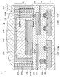
- FIG. 1 is a vertical sectional view illustrating the configuration of a photodetector according to the present embodiment.
- the photodetector according to the present embodiment is a device that multiplies the carriers generated by photoelectric conversion by avalanche in the pn junction region of a high electric field.
- the photodetector according to this embodiment may be a so-called single photon avalanche photodiode (SPAD).
- SPAD single photon avalanche photodiode
- the photodetector according to the present embodiment can form a pixel array by arranging a plurality of photodetectors in a matrix, for example. According to the pixel array using the photodetector according to the present embodiment, the light from the object can be detected with higher sensitivity and higher accuracy.
- the photodetector 1 is, for example, a first substrate in which a first semiconductor substrate 11 and a first wiring layer 12 are laminated, a second semiconductor substrate 21, and a second wiring layer 22. It can be configured as a laminated semiconductor device in which a second substrate in which is laminated is bonded.
- the microlens 33 is provided on the surface opposite to the surface on which the second wiring layer 22 of the second substrate is laminated.
- the incident light collected by the microlens 33 is converted into a signal charge by photoelectric conversion by a pn junction of a high electric field provided inside the second semiconductor substrate 21.
- the converted signal charge is transmitted to the first semiconductor substrate 11 via the second wiring layer 22 and the first wiring layer 12, and is converted into a detection signal for incident light by a logic circuit provided on the first semiconductor substrate 11.
- the photodetector 1 can detect the incident light and output a detection signal corresponding to the detected incident light.
- the photodetector 1 according to the present embodiment may be used in a so-called back-illuminated laminated imaging sensor.
- the first semiconductor substrate 11 is, for example, a silicon (Si) substrate.
- the first semiconductor substrate 11 may be a substrate formed of an elemental semiconductor other than silicon or a compound semiconductor.
- the first semiconductor substrate 11 may be further doped with a p-type impurity such as boron (B) or aluminum (Al) or an n-type impurity such as phosphorus (P) or arsenic (As) at a low concentration.
- the first semiconductor substrate 11 has a p-type region (p-well) 110P heavily doped with p-type impurities and an n-type region (n-well) 110N heavily doped with n-type impurities. Provided. However, when the first semiconductor substrate 11 is doped, the doping concentration of the p-type region 110P and the n-type region 110N is set to be higher than the doping concentration of the first semiconductor substrate 11.
- an n-type field effect transistor (FET) 111N is provided in the p-type region 110P, and a p-type field effect transistor (FET) 111P is provided in the n-type region 110N. That is, CMOS (complementary MOS) using the n-type FET 111N and the p-type FET 111P is formed on the first semiconductor substrate 11. As a result, a logic circuit for signal processing the signal charge photoelectrically converted by the second semiconductor substrate 21 can be formed on the first semiconductor substrate 11.
- CMOS complementary MOS
- the first wiring layer 12 is provided by laminating a wiring 121 that transmits a current or a voltage between a plurality of circuits or elements and an interlayer insulating film 120 that insulates the wiring 121 from each other.
- the wiring 121 is electrically connected by a contact penetrating the interlayer insulating film 120 in the thickness direction of the first wiring layer 12, so that each of the n-type FET 111N and the p-type FET 111P provided on the first semiconductor substrate 11 is provided.
- the terminals can be electrically connected.
- Wiring 121 and contacts are, for example, titanium (Ti), molybdenum (Mo), tantalum (Ta), tungsten (W), niobium (Nb), nickel (Ni), zirconium (Zr), gold (Au), silver ( It can be formed of a metal such as Ag), aluminum (Al) or copper (Cu), or a conductive material such as an alloy or metal compound thereof.
- the interlayer insulating film 120 can be formed of, for example, an insulating inorganic oxynitride such as silicon dioxide (SiO 2 ), silicon nitride (SiN), or silicon oxynitride (SiON).
- the second wiring layer 22 is laminated with a wiring 221 that transmits a current or a voltage between a plurality of circuits or elements and an interlayer insulating film 220 that insulates the wiring 221 from each other. It is provided by.
- the wiring 221 is electrically connected by a contact penetrating the interlayer insulating film 220 in the thickness direction of the second wiring layer 22, so that the signal charge is photoelectrically converted by the pn junction inside the second semiconductor substrate 21. Can be transmitted to the first wiring layer 12.
- Wiring 221 and contacts are, for example, titanium (Ti), molybdenum (Mo), tantalum (Ta), tungsten (W), niobium (Nb), nickel (Ni), zirconium (Zr), gold (Au), silver (Au). It can be formed of a metal such as Ag), aluminum (Al) or copper (Cu), or a conductive material such as an alloy or metal compound thereof.
- the interlayer insulating film 220 can be formed of, for example, an insulating inorganic oxynitride such as silicon dioxide (SiO 2 ), silicon nitride (SiN), or silicon oxynitride (SiON).
- first substrate and the second substrate are bonded so that the first wiring layer 12 and the second wiring layer 22 face each other.
- the wiring 121 included in the first wiring layer 12 and the wiring 221 included in the second wiring layer 22 join the electrodes exposed on the surfaces of the first wiring layer 12 and the second wiring layer 22 to each other. It can be electrically connected.
- electrodes are formed on the uppermost layers of the first wiring layer 12 and the second wiring layer 22, respectively. Therefore, the first wiring layer 12 and the second wiring layer 22 are bonded to each other so as to face each other, and the electrodes are brought into direct contact with each other to perform heat treatment, whereby the electrodes can be joined to each other.
- the photodetector 1 does not form a contact penetrating the interface between the first wiring layer 12 and the second wiring layer 22, and the wiring 121 of the first wiring layer 12 and the second wiring layer 12 are formed. 2 The wiring 221 of the wiring layer 22 can be electrically connected. According to this electrode bonding structure, the photodetector 1 can simplify the manufacturing process.
- the second semiconductor substrate 21 is, for example, a silicon (Si) substrate.
- the second semiconductor substrate 21 may be a substrate formed of an elemental semiconductor other than silicon or a compound semiconductor.
- the second semiconductor substrate 21 may be further doped with a p-type impurity such as boron (B) or aluminum (Al) or an n-type impurity such as phosphorus (P) or arsenic (As) at a low concentration.
- the second semiconductor substrate 21 is heavily doped with the first conductive type (for example, n-type) impurities and the first conductive type region 211 and the second conductive type (for example, p-type) impurities.
- the second conductive type region 212 is provided, respectively.
- the first conductive type region 211 is provided on the surface side on which the second wiring layer 22 of the second semiconductor substrate 21 is laminated, and the second conductive type region 212 is larger than the first conductive type region 211. It is provided inside the second semiconductor substrate 21 so as to be in contact with the first conductive type region 211.
- the second conductive type region 212 forms a pn junction at the interface with the first conductive type region 211, and avalanche multiplys the carriers generated by the incident light.
- the second conductive region 212 may be depleted in order to increase the detection efficiency (Photon Detection Efficiency: PDE) of the photodetector 1.
- PDE Photon Detection Efficiency
- the first conductive type region 211 and the second conductive type region 212 are also collectively referred to as a multiplying region 210.
- the inside of the second conductive type region 212 of the second semiconductor substrate 21 can be further depleted, so that the detection efficiency (PDE) of the photodetector 1 can be further improved. Can be enhanced.
- the doping concentration of the second semiconductor substrate 21 at this time may be lower than the doping concentration of the second conductive region 212.
- the first conductive type region 211 functions as a cathode for extracting avalanche-multiplied carriers (for example, holes) in the second conductive type region 212.
- the first conductive region 211 is electrically connected to the wiring 221 of the second wiring layer 22 via the contact, for example, in the contact region 211N doped with a higher concentration of the first conductive type (for example, n type) impurity. It may be connected to.
- the anode 213P for extracting the avalanche-multiplied carrier (for example, electrons) in the second conductive type region 212 is in the same layer as the first conductive type region 211, and the separation region 217 and the first conductive type described later. It is provided on the second semiconductor substrate 21 between the region 211.
- the anode 213P is doped with, for example, a second conductive type (for example, p type) impurity having a higher concentration than the hole accumulation region 213 described later, and is electrically connected to the wiring 221 of the second wiring layer 22 via a contact. You may be.
- the second conductive type region 212 may be provided in the projective region of the first conductive type region 211 when the surface of the second semiconductor substrate 21 is viewed in a plan view. That is, the second conductive type region 212 may be provided in a planar shape slightly smaller than the first conductive type region 211. In the vicinity of the separation region 217 that defines the pixel region, carriers that do not depend on photoelectric conversion are likely to occur. Therefore, by making the planar shape of the second conductive region 212 one size smaller than the planar shape of the first conductive region 211, carriers that do not depend on photoelectric conversion are multiplied by the avalanche in the second conductive region 212. The possibility can be reduced. According to this, the photodetector 1 can suppress the generation of a noise signal.
- the second semiconductor substrate 21 is further provided with a separation region 217 that determines the pixel region of the photodetector 1.
- the separation region 217 is provided so as to substantially surround the first conductive type region 211 and the second conductive type region 212, which are the multiplication region 210.
- the separation region 217 can prevent electrical crosstalk between pixels by electrically insulating the magnification region 210 for each pixel. According to this, a plurality of photodetectors 1 can be arranged in a matrix to form a pixel array.
- the separation region 217 can be composed of, for example, a metal film 214 that penetrates the second semiconductor substrate 21 in the thickness direction and an insulating film 215 that covers the side surface of the metal film 214.
- the metal film 214 can be formed of, for example, a metal that reflects light (for example, tungsten).
- the insulating film 215 can be formed of, for example, an insulating inorganic oxynitride (for example, SiO 2 ). According to this, in the separation region 217, the pixels can be optically separated by the metal film 214, and the pixels can be electrically separated by the insulating film 215.
- the second semiconductor substrate 21 is further provided with a hole accumulation region 213 in which holes are accumulated by being doped with a second conductive type (for example, p-type) impurity.
- the hole storage region 213 is provided on the second semiconductor substrate 21 in the pixel region along the side surface of the separation region 217. Further, the hole accumulation region 213 may be provided by extending to a surface opposite to the surface on which the second wiring layer 22 of the second substrate is laminated.
- the hole accumulation region 213 is provided in a region where different materials are in contact with each other to suppress a dark current generated at an interface between different materials.
- the hole accumulation region 213 may be in contact with the anode 213P.
- the anode 213P is in contact with the hole storage region 213 by being provided in a part of the surface of the second semiconductor substrate 21 among the hole storage regions 213 provided along the side surface of the separation region 217. You may.
- the photodetector 1 can adjust the bias voltage applied to the multiplication region 210 via the anode 213P and the hole storage region 213.
- the hole storage region 213 functions as a path for extracting carriers (for example, electrons) from the inside of the second semiconductor substrate 21 to the anode 213P, so that the on-resistance of the photodetector 1 can be reduced.
- an insulating region 216 is further provided on the second semiconductor substrate 21 between the first conductive type region 211 which is a cathode and the anode 213P.
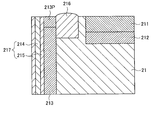
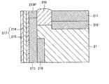
- FIG. 2A is a vertical cross-sectional view in which the region A of FIG. 1 is rotated by 180 ° and enlarged
- FIG. 2B is a vertical cross-sectional view showing a modified example of the structure shown in FIG. 2A.
- the insulating region 216 is made of an insulating material and is provided on the second semiconductor substrate 21 between the first conductive type region 211 which is a cathode and the anode 213P. According to this, the insulation region 216 can reduce the possibility of edge breakdown by relaxing the electric field between the first conductive region 211 and the anode 213P.
- the insulation region 216 is provided at a formation depth deeper than the formation depth of the first conductive type region 211. According to this, the insulating region 216 can further enhance the electric field relaxation effect between the first conductive type region 211 and the anode 213P.
- the insulating region 216 may be provided at a formation depth shallower than the formation depth of the second conductive type region 212. According to this, the insulating region 216 contains carriers (holes) that are not dependent on photoelectric conversion and are generated at the interface between the second semiconductor substrate 21 and the insulating region 216, which are made of different materials, in the second conductive type region 212. Can be recovered in the first conductive type region 211 without entering the first conductive type region 211. Therefore, the photodetector 1 can reduce the probability that the carrier that does not depend on photoelectric conversion is avalanche-multiplied in the second conductive region 212, so that the noise signal can be further reduced. The carriers (electrons) that do not depend on photoelectric conversion generated at the interface between the second semiconductor substrate 21 and the insulating region 216 are collected, for example, in the hole storage region 213 adjacent to the insulating region 216.
- the insulating region 216 can be formed of, for example, an insulating inorganic oxynitride such as silicon dioxide (SiO 2 ), silicon nitride (SiN), or silicon oxynitride (SiON). Specifically, in the insulating region 216, a part of a predetermined region of the second semiconductor substrate 21 is removed by etching or the like using an STI (Shallow Trench Isolation) method, and then the formed opening is formed by silicon oxide (SiO 2). ) May be formed by embedding.
- an insulating inorganic oxynitride such as silicon dioxide (SiO 2 ), silicon nitride (SiN), or silicon oxynitride (SiON).
- the insulating region 216 may exist between the first conductive type region 211, which is the cathode, and the anode 213P. Specifically, the insulating region 216 may not be in contact with the first conductive type region 211, and may not be in contact with the anode 213P. For example, as shown in FIG. 2B, the insulating region 216 may be provided at a distance from the first conductive type region 211. When the insulating region 216 and the first conductive type region 211 are separated from each other, the electric field concentration can be prevented between the insulating region 216 and the first conductive type region 211, so that the photodetector 1 has an edge breakdown. The possibility of
- the photodetector 1 when the insulating region 216 is provided in contact with the first conductive type region 211, the photodetector 1 can reduce the size of the pixel region, so that the photodetector 1 can detect light. It becomes possible to further miniaturize and increase the density of the pixel array using the device 1.
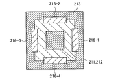
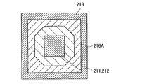
- FIG. 3 is a plan view showing a first plan arrangement example of the insulation region 216
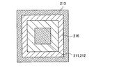
- FIG. 4 is a plan view showing a second plane arrangement example of the insulation region 216.
- FIGS. 3 and 4 in order to facilitate understanding, a case where the insulating region 216 and the first conductive type region 211 are provided apart from each other (example shown in FIG. 2B) will be illustrated. ..
- the shape of the pixel region defined by the separation region 217 is not limited to such an example.
- the shape of the pixel region may be a polygonal shape, and may be a triangle, a pentagon, a hexagon, or a polygonal shape other than a quadrangle.
- the pixel region defined by the separation region 217 has a polygonal shape, and the plurality of regions of the insulation region 216 are provided at positions corresponding to each side of the polygonal shape of the pixel region. Be done.
- the pixel region having the hole storage region 213 as the outer circumference has a quadrangular shape
- the insulating region 216 is a plurality of regions 216-1, 216-2, 216 separated from each other. It may be composed of -3, 216-4. Regions 216-1, 216-2, 216-3, and 216-4 may be provided at positions corresponding to each side of the quadrangular shape of the pixel region.
- the insulating region 216 is divided into a plurality of regions 216-1, 216-2, 216-3, and 216-4, carriers that do not depend on photoelectric conversion are released to the hole accumulation region 213.
- the route is secured in a plane. Therefore, according to the first planar arrangement example, it is possible to further reduce the possibility that carriers that do not depend on photoelectric conversion enter the second conductive type region 212 that performs avalanche multiplication, so that the photodetector 1 can be used.
- the noise signal can be suppressed.
- the positions where the plurality of regions 216-1, 216-2, 216-3, and 216-4 constituting the insulating region 216 are separated from each other are the positions corresponding to the vertices of the quadrangular shape. It has become. This is because the position corresponding to each vertex of the quadrangular shape has a longer distance between the first conductive type region 211 and the hole accumulation region 213 than the position corresponding to each side of the quadrangular shape, so that the insulating region 216 is not provided. This is because the possibility of edge breakdown is sufficiently low.
- the insulation region 216 can suppress the generation of noise signals while effectively suppressing edge breakdown.
- the pixel region defined by the separation region 217 has a polygonal shape, and the insulation region 216 is provided over the entire circumference of the polygonal shape of the pixel region.
- the pixel region having the hole storage region 213 as the outer circumference has a quadrangular shape, and the insulation region 216 is provided along the hole storage region 213 over the entire circumference of the pixel region. May be done.
- the insulating region 216 is provided isotropically and continuously, it is possible to suppress the variation in the characteristics of the insulating region 216 for each orientation. Further, since the formed region 216 is isotropic and continuous, the insulating region 216 can be formed by a simpler manufacturing process.
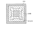
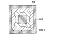
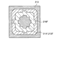
- FIGS. 5A to 5F are plan views showing a modified example of the second planar arrangement example of the insulating region 216. Also in the plan views shown in FIGS. 5A to 5F, in order to facilitate understanding, a case where the insulating region 216 and the first conductive type region 211 are provided apart from each other (example shown in FIG. 2B) will be illustrated. ..
- the insulating region 216A may be provided so that the width of the position corresponding to each vertex of the quadrangular shape of the pixel region is larger than the width of the position corresponding to each side of the quadrangular shape.
- the insulating region 216A is a line segment diagonally straddled between the two sides constituting each vertex of the quadrangular shape from a planar shape provided over the entire circumference of the quadrangular shape of the pixel region. It may have a flat shape overhanging to.
- the insulating region 216A may have a planar shape that extends from a planar shape provided over the entire circumference of the quadrangular shape of the pixel region to a triangular shape at a position corresponding to each apex of the quadrangular shape. ..
- the insulating region 216B may be provided so that the width of the position corresponding to each side of the quadrangular shape of the pixel region is larger than the width of the position corresponding to each vertex of the quadrangular shape. .. Specifically, the insulating region 216B has a planar shape that extends from a planar shape provided over the entire circumference of the quadrangular shape of the pixel region to a quadrangle at a position corresponding to each side of the quadrangular shape. May be good.
- the insulating region 216B can guide the carriers photoelectrically converted inside the second semiconductor substrate 21 to the second conductive type region 212 for avalanche multiplication. Specifically, the insulating region 216B closes the surface of the second semiconductor substrate 21 so that the carriers photoelectrically converted inside the second semiconductor substrate 21 do not enter the second conductive region 212 and the second semiconductor. It is possible to prevent the substrate 21 from reaching the surface.
- the insulating regions 216C to 216E may be provided so that the angle of each apex of the planar shape is larger than 90 degrees.
- the insulating region 216C shown in FIG. 5C has a polygonal shape in which each apex is diagonally cut from the polygonal shape of the insulating region 216 shown in FIG.
- the insulating region 216D shown in FIG. 5D has a polygonal shape in which each apex is diagonally cut from the polygonal shape of the insulating region 216A shown in FIG. 5A.
- the insulating region 216E shown in FIG. 5E has a polygonal shape in which each apex is diagonally cut from the polygonal shape of the insulating region 216B shown in FIG. 5B.
- the insulating regions 216C to 216E by setting the angle of each vertex of the planar shape to an obtuse angle of more than 90 degrees, it is possible to suppress the concentration of stress at each vertex. Therefore, the insulating regions 216C to 216E can prevent defects from occurring inside the second semiconductor substrate 21. According to this, the photodetector 1 can suppress the generation of carriers due to defects and the increase in dark current.
- the planar shapes of the first conductive type region 211F and the second conductive type region 212F are not limited to the quadrangular shape, and are triangular, five or more polygonal shapes, or polygonal shapes having irregularities. It may be in shape.
- the insulating region 216F can be changed in planar shape according to the planar shapes of the first conductive type region 211F and the second conductive type region 212F.
- the insulating region 216F may have a planar shape that becomes convex according to the convex shape of the planar shape of the first conductive type region 211F and the second conductive type region 212F, and the first conductive type region 211F and the first conductive type region 211F. 2
- the planar shape may be concave depending on the convex shape of the planar shape of the conductive region 212F.
- the insulating region 216F may have a planar shape that becomes convex according to the concave shape of the planar shape of the first conductive type region 211F and the second conductive type region 212F, and the first conductive type region 211F and The plane shape may be concave depending on the concave shape of the plane shape of the second conductive type region 212F.
- the photodetector 1 according to the present embodiment has been specifically described above.
- the insulation region 216 can relax the electric field between the first conductive region 211 which is the cathode and the anode 213P, and reduce the possibility of edge breakdown. .. Since the insulation region 216 has a high effect of electric field relaxation and can effectively reduce the possibility of edge breakdown at a shorter distance, the photodetector 1 can reduce the size of the pixel region. It is possible. According to this, the photodetector 1 can further miniaturize and increase the density of the pixel array using the photodetector 1.
- the photodetector 1 according to the present embodiment can be manufactured by using a technique, process, and device known as a method for manufacturing a semiconductor device. Therefore, the description of the details of the manufacturing method of the photodetector 1 according to the present embodiment will be omitted.
- FIG. 6 is a vertical cross-sectional view corresponding to FIG. 2A showing the cross-sectional shape of the insulating region 216G according to the first modification.
- the three-dimensional shape of the insulating region 216G may be a shape having a reverse taper in the thickness direction of the second semiconductor substrate 21.
- the three-dimensional shape of the insulating region 216G may be a reverse taper shape in which the diameter of the planar shape gradually decreases from the surface of the second semiconductor substrate 21 toward the inside. Since the three-dimensionally shaped insulating region 216G can suppress the concentration of stress in the thickness direction of the second semiconductor substrate 21, it is possible to prevent defects from occurring inside the second semiconductor substrate 21. it can. According to this, the photodetector 1 can suppress the generation of carriers due to the defect of the second semiconductor substrate 21 and the increase of dark current.
- the insulating region 216G having a three-dimensional shape having an inverted taper shape can be similarly applied to the planar insulating regions 216 and 216A to 216F of FIGS. 3 to 5F described above.
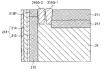
- FIG. 7A is a vertical cross-sectional view corresponding to FIG. 2A showing the cross-sectional shape of the insulating regions 216G-1 and 216G-2 according to the second modification.
- FIG. 7B is a plan view corresponding to FIG. 3 showing the plan shape of the insulating regions 216G-1 and 216G-2 according to the second modification.
- a plurality of insulating regions 216G-1 and 216G-2 may be provided side by side between the first conductive type region 211 which is a cathode and the anode 213P and the hole storage region 213.
- the insulating region 216G-2 is provided over the entire circumference of the polygonal shape of the pixel region, and the insulating region 216G-1 is entirely inside the insulating region 216G-2. It may be provided over the circumference. That is, the insulating regions 216G-1 and 216G-2 may be provided in a multi-ring shape.
- the photodetector 1 can further reduce the possibility of edge breakdown. Further, in the insulating regions 216G-1 and 216G-2, the optical path length of the light from the second wiring layer 22 side (for example, the reflected light from the wiring 221) is extended by the scattering effect, and the light path length is extended from the second wiring layer 22 side. Since the possibility that the light becomes noise can be reduced, the detection efficiency of the photodetector 1 can be further improved.
- FIG. 7A shows an example in which the three-dimensional shape of the insulating regions 216G-1 and 216G-2 is a reverse taper shape, but this modification is not limited to such an example.
- the three-dimensional shape of the insulating regions 216G-1 and 216G-2 may be a non-tapered shape as shown in FIG. 2A.
- FIG. 7B an example in which the insulating regions 216G-1 and 216G-2 are provided over the entire circumference of the polygonal shape of the pixel region is shown, but this modification is not limited to such an example.
- the insulating regions 216G-1 and 216G-2 may be divided into a plurality of regions by being separated in the circumferential direction of the polygonal shape of the pixel region.
- FIG. 8 is a vertical cross-sectional view corresponding to FIG. 2A showing a cross section of the second semiconductor substrate 21 according to the third modification.
- 9A to 9C are vertical cross-sectional views showing variations in the cross section of the second semiconductor substrate 21 shown in FIG.
- the second semiconductor substrate 21 inside the insulating region 216 may be provided with the same conductive type (for example, p-type) sub-storage region 218 as the hole storage region 213.
- the sub-accumulation region 218 is a region in which holes (holes) are accumulated by being doped with a second conductive type (for example, p-type) impurity, like the hole accumulation region 213. It is provided in contact with the side surface of the region 213.
- the sub-storage region 218 supports the function of the hole storage region 213 as a path for extracting carriers (for example, electrons) from the inside of the second semiconductor substrate 21 to the anode 213P. According to this, the photodetector 1 can further reduce the on-resistance.
- the photodetector 1 can further reduce the generation of noise signals due to carriers that do not depend on photoelectric conversion.
- the sub-storage region 218 can be provided in the projection region of the insulation region 216 when the surface of the second semiconductor substrate 21 is viewed in a plan view. If the sub-accumulation region 218 is excessively close to the first conductive region 211, unintended conduction may occur between the sub-accumulation region 218 and the first conductive region 211. Therefore, the sub storage region 218 is provided so as not to protrude from the region where the insulation region 216 is provided.
- the insulating region 216A shown in FIG. 5A it is possible to increase the region in which the sub-accumulation region 218 can be formed by increasing the plane region of the insulating region 216A.
- the insulating region 216A corresponds to each vertex of the polygonal shape of the pixel region at a position where the distance between the first conductive region 211 and the hole storage region 213 is relatively large.
- the plane area is increasing. According to this, since the region in which the sub-accumulation region 218 can be formed can be made wider, the photodetector 1 can further reduce the on-resistance.
- the sub storage area 218 may be provided in all the areas where the insulating area 216 is provided, or may be provided in a part of the area where the insulating area 216 is provided.
- the first conductive type region 211, the insulating region 216, and the sub-accumulation region 218 do not have to be in contact with each other.
- the first conductive type region 211 and the insulating region 216 do not have to be in contact with each other.
- the insulating region 216 and the sub-accumulation region 218 do not have to be in contact with each other. In such a case, it is not necessary to study the manufacturing process conditions for strictly controlling the formation depth of the insulating region 216 and the formation depth of the sub-accumulation region 218, so that the photodetector 1 can be manufactured more easily. It becomes.
- a second conductive type (for example, p-type) impurity is provided as in the sub-accumulation region 218 and the hole accumulation region 213.
- a low concentration region 218A doped with is further provided.
- the low concentration region 218A has the same function as the sub-accumulation region 218, but the doping concentration of the second conductive type (for example, p-type) impurity is lower than the doping concentration of the sub-accumulation region 218.
- a separation area provided on the semiconductor substrate that defines the pixel area A hole storage region provided on the semiconductor substrate in the pixel region along the side surface of the separation region, A magnification region provided on the semiconductor substrate in the pixel region and formed by joining a first conductive type region and a second conductive type region from the surface side of the semiconductor substrate in the thickness direction of the semiconductor substrate.
- the photodetector according to (7) wherein the width of the insulating region corresponding to each vertex of the pixel region is smaller than the width of the insulating region corresponding to each side of the pixel region.
- the planar shape of the insulating region is a polygonal shape.
- (11) The photodetector according to any one of (1) to (10), wherein a plurality of the insulating regions are provided side by side between the multiplication region and the hole storage region.
- the separation region is any one of (1) to (15), which is composed of a double structure of a metal film extending in the thickness direction of the semiconductor substrate and an insulating film covering the side surface of the metal film. The photodetector described in the section.
- Optical detector 11 1st semiconductor substrate 12 1st wiring layer 21 2nd semiconductor substrate 22 2nd wiring layer 33 Microlens 110N n-type region 110P p-type region 111N n-type field effect transistor 111P p-type field effect transistor 120, 220 Interlayer insulation film 121, 221 Wiring 210 Multiplying area 211 First conductive type area 212 Second conductive type area 213 Hole storage area 213P Anodic 214 Metal film 215 Insulation film 216 Insulation area 217 Separation area 218 Sub storage area
Landscapes
- Light Receiving Elements (AREA)
- Solid State Image Pick-Up Elements (AREA)
Abstract
半導体基板に設けられ、画素領域を画定する分離領域と、前記分離領域の側面に沿って前記画素領域の前記半導体基板に設けられたホール蓄積領域と、前記画素領域の前記半導体基板に設けられ、前記半導体基板の表面側から第1導電型領域、及び第2導電型領域を前記半導体基板の厚み方向に接合することで構成された増倍領域と、前記増倍領域と、前記ホール蓄積領域との間の領域の前記半導体基板に設けられた絶縁領域と、を備え、前記絶縁領域の形成深さは、前記第1導電型領域の形成深さよりも深い、光検出器。
Description
本開示は、光検出器に関する。
光を電子に変換するフォトダイオードの1つとして、アバランシェフォトダイオード(APD)が知られている。APDは、アバランシェ現象を利用することで、100%を超える光電変換効率を実現することが可能なフォトダイオードである。
特に、ブレークダウン電圧よりも高い印加電圧で動作させたAPDは、光電変換にて生じたキャリアによって電子雪崩を発生させることができるため、キャリアの増倍を行うことができる。このようなAPDは、1個のフォトンを検出することもできるため、シングルフォトンアバランシェフォトダイオード(SPAD)とも称される。
例えば、下記の特許文献1には、SPADが配列されたフォトダイオードアレイにおいて、画素間に分離領域を形成することで隣接画素へのクロストークを低減する技術が開示されている。
しかし、特許文献1に記載されたSPADでは、エッジブレークダウンの抑制について十分な検討がなされていなかった。エッジブレークダウンは、構造等に依存して局所的に電界が高くなり、意図せずにブレークダウンしてしまう現象である。SPADは、pn接合に高電界が印加されるため、このようなエッジブレークダウンを抑制することが重要となる。
例えば、エッジブレークダウンを抑制するためには、SPADのカソード及びアノードの間の距離を大きくすることが考えられる。しかしながら、このような場合、SPADの面積が大きくなってしまうため、SPADを行列状に複数配列させた画素アレイを形成する場合に画素アレイの微細化及び高密度化が困難となる。
そこで、本開示では、微細化及び高密度化に適した構造にてエッジブレークダウンを抑制することが可能な、新規かつ可利用された光検出器を提案する。
本開示によれば、半導体基板に設けられ、画素領域を画定する分離領域と、前記分離領域の側面に沿って前記画素領域の前記半導体基板に設けられたホール蓄積領域と、前記画素領域の前記半導体基板に設けられ、前記半導体基板の表面側から第1導電型領域、及び第2導電型領域を前記半導体基板の厚み方向に接合することで構成された増倍領域と、前記増倍領域と、前記ホール蓄積領域との間の領域の前記半導体基板に設けられた絶縁領域と、を備え、前記絶縁領域の形成深さは、前記第1導電型領域の形成深さよりも深い、光検出器が提供される。
以下に添付図面を参照しながら、本開示の好適な実施の形態について詳細に説明する。なお、本明細書及び図面において、実質的に同一の機能構成を有する構成要素については、同一の符号を付することにより重複説明を省略する。
以下の説明にて参照する各図面では、説明の便宜上、一部の構成部材の大きさを誇張して表現している場合がある。したがって、各図面において図示される構成部材同士の相対的な大きさは、必ずしも実際の構成部材同士の大小関係を正確に表現するものではない。
なお、説明は以下の順序で行うものとする。
1.光検出器
1.1.光検出器の構成
1.2.絶縁領域の平面配置
2.変形例
2.1.第1の変形例
2.2.第2の変形例
2.3.第3の変形例
1.光検出器
1.1.光検出器の構成
1.2.絶縁領域の平面配置
2.変形例
2.1.第1の変形例
2.2.第2の変形例
2.3.第3の変形例
<1.光検出器>
(1.1.光検出器の構成)
まず、図1~図2Bを参照して、本開示の一実施形態に係る光検出器の構成について説明する。図1は、本実施形態に係る光検出器の構成を説明する縦断面図である。
(1.1.光検出器の構成)
まず、図1~図2Bを参照して、本開示の一実施形態に係る光検出器の構成について説明する。図1は、本実施形態に係る光検出器の構成を説明する縦断面図である。
本実施形態に係る光検出器は、光電変換により発生したキャリアを高電界のpn接合領域でアバランシェ増倍するデバイスである。本実施形態に係る光検出器は、いわゆるシングルフォトンアバランシェフォトダイオード(SPAD)であってもよい。
本実施形態に係る光検出器は、例えば、行列状に複数配列されることで画素アレイを形成することができる。本実施形態に係る光検出器を用いた画素アレイによれば、対象物からの光をより高感度及び高精度で検出することができる。
図1に示すように、本実施形態に係る光検出器1は、例えば、第1半導体基板11及び第1配線層12を積層した第1基板と、第2半導体基板21及び第2配線層22を積層した第2基板とを貼り合わせた積層型の半導体装置として構成することができる。
光検出器1では、第2基板の第2配線層22が積層された面と反対側の面にマイクロレンズ33が設けられる。マイクロレンズ33にて集光された入射光は、第2半導体基板21の内部に設けられた高電界のpn接合によって光電変換されることで、信号電荷に変換される。変換された信号電荷は、第2配線層22及び第1配線層12を介して第1半導体基板11に伝達され、第1半導体基板11に設けられた論理回路によって入射光に対する検出信号に変換される。このような動作によって、光検出器1は、入射光を検出し、検出した入射光に対応する検出信号を出力することができる。本実施形態に係る光検出器1は、いわゆる裏面照射型の積層撮像センサに用いられてもよい。
第1半導体基板11は、例えば、シリコン(Si)基板である。ただし、第1半導体基板11は、シリコン以外の元素半導体、又は化合物半導体で形成された基板であってもよい。第1半導体基板11は、さらに、ホウ素(B)若しくはアルミニウム(Al)などのp型不純物、又はリン(P)若しくはヒ素(As)などのn型不純物によって低濃度でドーピングされていてもよい。
第1半導体基板11には、p型不純物によって高濃度にドーピングされたp型領域(p-ウェル)110P、及びn型不純物によって高濃度にドーピングされたn型領域(n-ウェル)110Nがそれぞれ設けられる。ただし、第1半導体基板11がドーピングされている場合、p型領域110P、及びn型領域110Nのドーピング濃度は、第1半導体基板11のドーピング濃度よりも高濃度とする。
p型領域110Pには、例えば、n型電界効果トランジスタ(FET)111Nが設けられ、n型領域110Nには、p型電界効果トランジスタ(FET)111Pが設けられる。すなわち、第1半導体基板11には、n型FET111N及びp型FET111Pを用いたCMOS(相補型MOS)が形成される。これにより、第1半導体基板11には、第2半導体基板21にて光電変換された信号電荷を信号処理するための論理回路が形成され得る。
第1配線層12は、複数の回路又は素子の間で電流又は電圧を伝達する配線121と、配線121の間を互いに絶縁する層間絶縁膜120とを積層することで設けられる。配線121は、層間絶縁膜120を第1配線層12の厚さ方向に貫通するコンタクトによって電気的に接続されることで、第1半導体基板11に設けられたn型FET111N及びp型FET111Pの各端子を電気的に接続することができる。
配線121及びコンタクトは、例えば、チタン(Ti)、モリブデン(Mo)、タンタル(Ta)、タングステン(W)、ニオブ(Nb)、ニッケル(Ni)、ジルコニウム(Zr)、金(Au)、銀(Ag)、アルミニウム(Al)若しくは銅(Cu)等の金属、又はこれらの合金若しくは金属化合物等の導電型材料にて形成することができる。層間絶縁膜120は、例えば、二酸化シリコン(SiO2)、窒化シリコン(SiN)、又は酸窒化シリコン(SiON)などの絶縁性の無機酸窒化物で形成することができる。
第2配線層22は、第1配線層12と同様に、複数の回路又は素子の間で電流又は電圧を伝達する配線221と、配線221の間を互いに絶縁する層間絶縁膜220とを積層することで設けられる。配線221は、層間絶縁膜220を第2配線層22の厚さ方向に貫通するコンタクトによって電気的に接続されることで、第2半導体基板21の内部のpn接合にて光電変換された信号電荷を第1配線層12に伝達することができる。
配線221及びコンタクトは、例えば、チタン(Ti)、モリブデン(Mo)、タンタル(Ta)、タングステン(W)、ニオブ(Nb)、ニッケル(Ni)、ジルコニウム(Zr)、金(Au)、銀(Ag)、アルミニウム(Al)若しくは銅(Cu)等の金属、又はこれらの合金若しくは金属化合物等の導電型材料にて形成することができる。層間絶縁膜220は、例えば、二酸化シリコン(SiO2)、窒化シリコン(SiN)、又は酸窒化シリコン(SiON)などの絶縁性の無機酸窒化物で形成することができる。
ここで、第1基板と、第2基板とは、第1配線層12と、第2配線層22とが対向するように貼り合わせられる。第1配線層12に含まれる配線121と、第2配線層22に含まれる配線221とは、第1配線層12、及び第2配線層22のそれぞれの表面に露出された電極同士を接合することで電気的に接続され得る。
具体的には、第1配線層12及び第2配線層22の最上層には、それぞれ電極が形成される。したがって、第1配線層12と、第2配線層22とを互いに対向するように貼り合わせ、互いの電極を直接接触させて熱処理を行うことで、互いの電極を接合させることができる。このような電極接合構造によれば、光検出器1では、第1配線層12及び第2配線層22の界面を貫通するコンタクトを形成することなく、第1配線層12の配線121と、第2配線層22の配線221とを電気的に接続することができる。この電極接合構造によれば、光検出器1は、製造工程を簡略化することができる。
第2半導体基板21は、例えば、シリコン(Si)基板である。ただし、第2半導体基板21は、シリコン以外の元素半導体、又は化合物半導体で形成された基板であってもよい。第2半導体基板21は、さらに、ホウ素(B)若しくはアルミニウム(Al)などのp型不純物、又はリン(P)若しくはヒ素(As)などのn型不純物によって低濃度でドーピングされていてもよい。
第2半導体基板21には、第1導電型(例えば、n型)不純物で高濃度にドーピングされた第1導電型領域211と、第2導電型(例えば、p型)不純物で高濃度にドーピングされた第2導電型領域212とがそれぞれ設けられる。具体的には、第1導電型領域211は、第2半導体基板21の第2配線層22が積層された面側に設けられ、第2導電型領域212は、第1導電型領域211よりも第2半導体基板21の内部に、第1導電型領域211と接するように設けられる。
第2導電型領域212は、第1導電型領域211との界面にてpn接合を形成しており、入射光によって生じたキャリアをアバランシェ増倍する。例えば、第2導電型領域212は、光検出器1の検出効率(Photon Detection Efficiency:PDE)を高めるために、空乏化されていてもよい。なお、本明細書では、第1導電型領域211、及び第2導電型領域212を併せて増倍領域210とも称する。
なお、第2半導体基板21がドーピングされている場合、第2半導体基板21の第2導電型領域212からさらに内部を空乏化させることができるため、光検出器1の検出効率(PDE)をさらに高めることができる。このときの第2半導体基板21のドーピング濃度は、第2導電型領域212のドーピング濃度より低くともよい。
第1導電型領域211は、第2導電型領域212にてアバランシェ増倍されたキャリア(例えば、正孔)を取り出すためのカソードとして機能する。第1導電型領域211は、例えば、より高濃度の第1導電型(例えば、n型)不純物でドーピングされたコンタクト領域211Nにて、コンタクトを介して第2配線層22の配線221と電気的に接続していてもよい。
一方、第2導電型領域212にてアバランシェ増倍されたキャリア(例えば、電子)を取り出すためのアノード213Pは、第1導電型領域211と同層、かつ後述する分離領域217と第1導電型領域211との間の第2半導体基板21に設けられる。アノード213Pは、例えば、後述するホール蓄積領域213よりも高濃度の第2導電型(例えば、p型)不純物でドーピングされ、コンタクトを介して第2配線層22の配線221と電気的に接続していてもよい。
なお、第2導電型領域212は、第2半導体基板21の表面を平面視した際に第1導電型領域211の射影領域内に設けられてもよい。すなわち、第2導電型領域212は、第1導電型領域211よりも一回り小さな平面形状にて設けられてもよい。画素領域を画定する分離領域217の近傍では、光電変換に依らないキャリアが発生しやすい。したがって、第2導電型領域212の平面形状を第1導電型領域211の平面形状よりも一回り小さくすることで、光電変換に依らないキャリアが第2導電型領域212にてアバランシェ増倍される可能性を低減することができる。これによれば、光検出器1は、ノイズ信号の発生を抑制することができる。
第2半導体基板21には、さらに、光検出器1の画素領域を確定する分離領域217が設けられる。具体的には、分離領域217は、増倍領域210である第1導電型領域211及び第2導電型領域212の周囲を平面的に囲むように設けられる。分離領域217は、増倍領域210を画素ごとに電気的に絶縁することで、画素間での電気的なクロストークを防止することができる。これによれば、光検出器1は、行列状に複数配列されることで、画素アレイを形成することができる。
分離領域217は、例えば、第2半導体基板21を厚さ方向に貫通する金属膜214と、金属膜214の側面を覆う絶縁膜215と、にて構成することができる。金属膜214は、例えば、光を反射する金属(例えば、タングステンなど)で形成することができる。絶縁膜215は、例えば、絶縁性を有する無機酸窒化物(例えば、SiO2など)で形成することができる。これによれば、分離領域217は、金属膜214によって画素間を光学的に分離し、かつ絶縁膜215によって画素間を電気的に分離することができる。
第2半導体基板21には、さらに、第2導電型(例えば、p型)不純物でドーピングされることで正孔(ホール)を蓄積したホール蓄積領域213が設けられる。具体的には、ホール蓄積領域213は、分離領域217の側面に沿って画素領域の第2半導体基板21に設けられる。また、ホール蓄積領域213は、第2基板の第2配線層22が積層された面と反対側の面にも延伸して設けられてもよい。ホール蓄積領域213は、異なる材質が接する領域に設けられることで、異なる材質の界面で発生する暗電流を抑制する。
また、ホール蓄積領域213は、アノード213Pと接していてもよい。具体的には、アノード213Pは、分離領域217の側面に沿って設けられたホール蓄積領域213のうち第2半導体基板21の表面の一部領域に設けられることで、ホール蓄積領域213と接していてもよい。これによれば、光検出器1は、アノード213P及びホール蓄積領域213を介して、増倍領域210に印加されるバイアス電圧を調整することが可能となる。また、ホール蓄積領域213は、第2半導体基板21の内部からアノード213Pへキャリア(例えば、電子)を取り出すためのパスとして機能することで、光検出器1のオン抵抗を低減させることができる。
本実施形態に係る光検出器1では、カソードである第1導電型領域211と、アノード213Pとの間の第2半導体基板21に絶縁領域216がさらに設けられる。
ここで、図2A及び図2Bを参照して、絶縁領域216の構成について具体的に説明する。図2Aは、図1の領域Aを180°回転させて拡大した縦断面図であり、図2Bは、図2Aで示した構造の変形例を示す縦断面図である。
図2Aに示すように、絶縁領域216は、絶縁性材料で構成され、カソードである第1導電型領域211と、アノード213Pとの間の第2半導体基板21に設けられる。これによれば、絶縁領域216は、第1導電型領域211と、アノード213Pとの間の電界を緩和することで、エッジブレークダウンの可能性を低減することができる。
絶縁領域216は、第1導電型領域211の形成深さよりも深い形成深さにて設けられる。これによれば、絶縁領域216は、第1導電型領域211と、アノード213Pとの間の電界緩和効果をより強くすることができる。
一方、絶縁領域216は、第2導電型領域212の形成深さよりも浅い形成深さにて設けられてもよい。これによれば、絶縁領域216は、互いに異なる材質で構成される第2半導体基板21と絶縁領域216との界面で生じた、光電変換に依らないキャリア(正孔)を第2導電型領域212に進入させずに第1導電型領域211にて回収することができる。したがって、光検出器1は、光電変換に依らないキャリアが第2導電型領域212でアバランシェ増倍される確率を低下させることができるため、ノイズ信号をより低減することができる。なお、第2半導体基板21と絶縁領域216との界面で生じた、光電変換に依らないキャリア(電子)は、例えば、絶縁領域216と隣接するホール蓄積領域213に回収される。
絶縁領域216は、例えば、二酸化シリコン(SiO2)、窒化シリコン(SiN)、又は酸窒化シリコン(SiON)などの絶縁性の無機酸窒化物で形成することができる。具体的には、絶縁領域216は、STI(Shallow Trench Isolation)法を用いて、第2半導体基板21の所定領域の一部をエッチング等で除去した後、形成された開口を酸化シリコン(SiO2)で埋め込むことで形成されてもよい。
なお、絶縁領域216は、カソードである第1導電型領域211と、アノード213Pとの間に存在すればよい。具体的には、絶縁領域216は、第1導電型領域211と接していなくともよく、アノード213Pと接していなくともよい。例えば、図2Bに示すように、絶縁領域216は、第1導電型領域211と離隔して設けられてもよい。絶縁領域216と第1導電型領域211とが離隔される場合、絶縁領域216と第1導電型領域211との間で電界集中を防止することができるため、光検出器1は、エッジブレークダウンの可能性をより低減することができる。
一方で、図2Aで示したように、絶縁領域216が第1導電型領域211と接して設けられる場合、光検出器1は、画素領域の大きさをより小さくすることができるため、光検出器1を用いた画素アレイをより微細化及び高密度化することが可能になる。
(1.2.絶縁領域の平面配置)
次に、図3及び図4を参照して、絶縁領域216の平面配置について具体的に説明する。図3は、絶縁領域216の第1の平面配置例を示す平面図であり、図4は、絶縁領域216の第2の平面配置例を示す平面図である。図3及び図4で示す平面図では、理解を容易にするために、絶縁領域216と、第1導電型領域211とが互いに離隔して設けられた場合(図2Bで示す例)について例示する。
次に、図3及び図4を参照して、絶縁領域216の平面配置について具体的に説明する。図3は、絶縁領域216の第1の平面配置例を示す平面図であり、図4は、絶縁領域216の第2の平面配置例を示す平面図である。図3及び図4で示す平面図では、理解を容易にするために、絶縁領域216と、第1導電型領域211とが互いに離隔して設けられた場合(図2Bで示す例)について例示する。
以下では、分離領域217にて画定された画素領域が四角形形状である場合を例示して説明を行うが、分離領域217にて画定された画素領域の形状は、かかる例示に限定されない。画素領域の形状は、多角形形状であればよく、四角形以外の三角形、五角形、六角形、又はそれ以上の多角形形状であってもよい。
第1の平面配置例では、分離領域217にて画定された画素領域は、多角形形状であり、絶縁領域216の複数の領域は、画素領域の多角形形状の各辺に対応する位置に設けられる。具体的には、図3に示すように、ホール蓄積領域213を外周とする画素領域は、四角形形状であり、絶縁領域216は、互いに離隔された複数の領域216-1、216-2、216-3、216-4にて構成されてもよい。領域216-1、216-2、216-3、216-4は、画素領域の四角形形状の各辺に対応する位置に設けられてもよい。
図3で示す平面配置例では、絶縁領域216が複数の領域216-1、216-2、216-3、216-4に分かれているため、光電変換に依らないキャリアをホール蓄積領域213に逃がす経路が平面的に確保されている。したがって、第1の平面配置例によれば、アバランシェ増倍を行う第2導電型領域212に光電変換に依らないキャリアが進入する可能性をより低減することができるため、光検出器1は、ノイズ信号を抑制することができる。
図3で示す平面配置例では、絶縁領域216を構成する複数の領域216-1、216-2、216-3、216-4が互い離隔される位置は、四角形形状の各頂点に対応する位置となっている。これは、四角形形状の各頂点に対応する位置は、四角形形状の各辺に対応する位置よりも第1導電型領域211と、ホール蓄積領域213との距離が長いため、絶縁領域216を設けなくともエッジブレークダウンの可能性が十分に低いためである。
したがって、第1の平面配置例によれば、絶縁領域216は、エッジブレークダウンを効果的に抑制しつつ、ノイズ信号の発生を抑制することが可能である。
第2の平面配置例では、分離領域217にて画定された画素領域は、多角形形状であり、絶縁領域216は、画素領域の多角形形状の全周に亘って設けられる。具体的には、図4に示すように、ホール蓄積領域213を外周とする画素領域は、四角形形状であり、絶縁領域216は、ホール蓄積領域213に沿って画素領域の全周に亘って設けられてもよい。
図4で示す平面配置例では、絶縁領域216が等方的かつ連続的に設けられているため、方位ごとに絶縁領域216の特性がばらつくことを抑制することができる。また、絶縁領域216は、形成された領域が等方的かつ連続的であるため、より容易な製造プロセスにて形成することができる。
続いて、図5A~図5Fを参照して、第2の平面配置例の変形例について説明する。図5A~図5Fは、絶縁領域216の第2の平面配置例の変形例を示す平面図である。図5A~図5Fで示す平面図でも、理解を容易にするために、絶縁領域216と、第1導電型領域211とが互いに離隔して設けられた場合(図2Bで示す例)について例示する。
図5Aで示すように、絶縁領域216Aは、画素領域の四角形形状の各頂点に対応する位置の幅が該四角形形状の各辺に対応する位置の幅よりも大きくなるように設けられ得る。具体的には、絶縁領域216Aは、画素領域の四角形状の全周に亘って設けられた平面形状から、該四角形形状の各頂点をそれぞれ構成する二辺の間に斜めに架け渡した線分まで張り出した平面形状となっていてもよい。換言すると、絶縁領域216Aは、画素領域の四角形形状の全周に亘って設けられた平面形状から、該四角形形状の各頂点に対応する位置にて三角形に張り出した平面形状となっていてもよい。
また、図5Bに示すように、絶縁領域216Bは、画素領域の四角形形状の各辺に対応する位置の幅が該四角形形状の各頂点に対応する位置の幅よりも大きくなるように設けられ得る。具体的には、絶縁領域216Bは、画素領域の四角形形状の全周に亘って設けられた平面形状から、該四角形形状の各辺に対応する位置にて四角形に張り出した平面形状となっていてもよい。
このような平面配置によれば、絶縁領域216Bは、アバランシェ増倍を行う第2導電型領域212へ第2半導体基板21の内部で光電変換されたキャリアを誘導することができる。具体的には、絶縁領域216Bは、第2半導体基板21の表面を塞ぐことで、第2半導体基板21の内部で光電変換されたキャリアが第2導電型領域212に進入せずに第2半導体基板21の表面に到達することを抑制することができる。
また、図5C~図5Eに示すように、絶縁領域216C~216Eは、平面形状の各頂点の角度が90度よりも大きくなるように設けられてもよい。具体的には、図5Cに示す絶縁領域216Cは、図5に示す絶縁領域216の多角形形状から各頂点を斜めに切断した多角形形状となっている。また、図5Dに示す絶縁領域216Dは、図5Aに示す絶縁領域216Aの多角形形状から各頂点を斜めに切断した多角形形状となっている。さらに、図5Eに示す絶縁領域216Eは、図5Bに示す絶縁領域216Bの多角形形状から各頂点を斜めに切断した多角形形状となっている。
このような平面配置によれば、絶縁領域216C~216Eは、平面形状の各頂点の角度を90度超の鈍角とすることで、各頂点にて応力が集中することを抑制することができる。したがって、絶縁領域216C~216Eは、第2半導体基板21の内部に欠陥が生じることを防止することができる。これによれば、光検出器1は、欠陥に起因してキャリアが発生し、暗電流が増加することを抑制することができる。
さらに、図5Fに示すように、第1導電型領域211F、及び第2導電型領域212Fの平面形状も四角形形状に限定されず、三角形形状又は五以上の多角形形状、又は凹凸を有する多角形形状であってもよい。このような場合、絶縁領域216Fは、第1導電型領域211F、及び第2導電型領域212Fの平面形状に応じて、平面形状を変化させることも可能である。例えば、絶縁領域216Fは、第1導電型領域211F、及び第2導電型領域212Fの平面形状の凸形状に応じて凸となる平面形状であってもよく、第1導電型領域211F、及び第2導電型領域212Fの平面形状の凸形状に応じて凹となる平面形状であってもよい。逆に、絶縁領域216Fは、第1導電型領域211F、及び第2導電型領域212Fの平面形状の凹形状に応じて凸となる平面形状であってもよく、第1導電型領域211F、及び第2導電型領域212Fの平面形状の凹形状に応じて凹となる平面形状であってもよい。
以上にて、本実施形態に係る光検出器1について具体的に説明した。本実施形態に係る光検出器1は、絶縁領域216によって、カソードである第1導電型領域211と、アノード213Pとの間の電界を緩和し、エッジブレークダウンの可能性を低減することができる。絶縁領域216は、電界緩和の効果が高く、より短い距離で効果的にエッジブレークダウンの可能性を低減することができるため、光検出器1は、画素領域の大きさをより小さくすることが可能である。これによれば、光検出器1は、光検出器1を用いた画素アレイをより微細化及び高密度化することが可能になる。
なお、本実施形態に係る光検出器1は、半導体装置の製造方法として公知の技術、工程、及び装置を用いることで製造することが可能である。よって、本実施形態に係る光検出器1の製造方法の詳細についての記載は省略する。
<2.変形例>
次に、図6~図9Cを参照して、本実施形態に係る光検出器1の第1~第3の変形例について説明する。
次に、図6~図9Cを参照して、本実施形態に係る光検出器1の第1~第3の変形例について説明する。
(2.1.第1の変形例)
まず、図6を参照して、本実施形態に係る光検出器1の第1の変形例について説明する。図6は、第1の変形例に係る絶縁領域216Gの断面形状を示す図2Aに対応する縦断面図である。
まず、図6を参照して、本実施形態に係る光検出器1の第1の変形例について説明する。図6は、第1の変形例に係る絶縁領域216Gの断面形状を示す図2Aに対応する縦断面図である。
図2Aに示すように、絶縁領域216Gの立体形状は、第2半導体基板21の厚み方向に逆テーパとなる形状であってもよい。具体的には、絶縁領域216Gの立体形状は、第2半導体基板21の表面から内部に向かって平面形状の径が徐々に小さくなっていくような逆テーパ形状であってもよい。このような立体形状の絶縁領域216Gは、第2半導体基板21の厚み方向に応力が集中することを抑制することができるため、第2半導体基板21の内部に欠陥が生じることを防止することができる。これによれば、光検出器1は、第2半導体基板21の欠陥に起因してキャリアが発生し、暗電流が増加することを抑制することができる。
なお、立体形状が逆テーパ形状である絶縁領域216Gは、上述した図3~図5Fの平面形状の絶縁領域216、216A~216Fに対しても同様に適用可能である。
(2.2.第2の変形例)
次に、図7A及び図7Bを参照して、本実施形態に係る光検出器1の第2の変形例について説明する。図7Aは、第2の変形例に係る絶縁領域216G-1、216G-2の断面形状を示す図2Aに対応する縦断面図である。図7Bは、第2の変形例に係る絶縁領域216G-1、216G-2の平面形状を示す図3に対応する平面図である。
次に、図7A及び図7Bを参照して、本実施形態に係る光検出器1の第2の変形例について説明する。図7Aは、第2の変形例に係る絶縁領域216G-1、216G-2の断面形状を示す図2Aに対応する縦断面図である。図7Bは、第2の変形例に係る絶縁領域216G-1、216G-2の平面形状を示す図3に対応する平面図である。
図7Aに示すように、絶縁領域216G-1、216G-2は、カソードである第1導電型領域211と、アノード213P及びホール蓄積領域213との間に、複数並んで設けられてもよい。具体的には、図7Bに示すように、絶縁領域216G-2は、画素領域の多角形形状の全周に亘って設けられ、絶縁領域216G-1は、絶縁領域216G-2の内部に全周に亘って設けられてもよい。すなわち、絶縁領域216G-1、216G-2は、多重リング形状にて設けられてもよい。
絶縁領域216G-1、216G-2は、画素領域の中心から外側に向かう方向において複数設けられることで、カソードである第1導電型領域211と、アノード213Pとの間の電界をより緩和することができる。これによれば、光検出器1は、エッジブレークダウンの可能性をより低減することができる。また、絶縁領域216G-1、216G-2は、散乱効果によって第2配線層22側からの光(例えば、配線221からの反射光など)の光路長を伸ばし、第2配線層22側からの光がノイズとなる可能性を低減することができるため、光検出器1の検出効率をより高めることができる。
なお、図7Aでは、絶縁領域216G-1、216G-2の立体形状が逆テーパ形状である例を示したが、本変形例はかかる例示に限定されない。絶縁領域216G-1、216G-2の立体形状は、図2Aで示したような非テーパ形状であってもよい。また、図7Bでは、絶縁領域216G-1、216G-2が画素領域の多角形形状の全周に亘って設けられる例を示したが、本変形例はかかる例示に限定されない。絶縁領域216G-1、216G-2は、画素領域の多角形形状の周方向に離隔されることで、複数の領域に分かれていてもよい。
(2.3.第3の変形例)
さらに、図8~図9Cを参照して、本実施形態に係る光検出器1の第3の変形例について説明する。図8は、第3の変形例に係る第2半導体基板21の断面を示す図2Aに対応する縦断面図である。図9A~図9Cは、図8に示す第2半導体基板21の断面のバリエーションを示す縦断面図である。
さらに、図8~図9Cを参照して、本実施形態に係る光検出器1の第3の変形例について説明する。図8は、第3の変形例に係る第2半導体基板21の断面を示す図2Aに対応する縦断面図である。図9A~図9Cは、図8に示す第2半導体基板21の断面のバリエーションを示す縦断面図である。
図8に示すように、絶縁領域216よりも内部の第2半導体基板21には、ホール蓄積領域213と同じ導電型(例えば、p型)のサブ蓄積領域218が設けられてもよい。具体的には、サブ蓄積領域218は、ホール蓄積領域213と同様に、第2導電型(例えば、p型)不純物でドーピングされることで正孔(ホール)を蓄積した領域であり、ホール蓄積領域213の側面に接して設けられる。サブ蓄積領域218は、第2半導体基板21の内部からアノード213Pへキャリア(例えば、電子)を取り出すためのパスとして、ホール蓄積領域213の機能をサポートする。これによれば、光検出器1は、オン抵抗をさらに低減させることができる。
また、サブ蓄積領域218は、ホール蓄積領域213と同様に、絶縁領域216と、第2半導体基板21との界面で生じるキャリア(例えば、電子)を回収することができる。これによれば、光検出器1は、光電変換に依らないキャリアに起因するノイズ信号の発生をより低減することができる。
ただし、サブ蓄積領域218は、第2半導体基板21の表面を平面視した際に絶縁領域216の射影領域内に設けられ得る。サブ蓄積領域218が第1導電型領域211に過度に接近した場合、サブ蓄積領域218と、第1導電型領域211との間で意図しない導通が生じる可能性がある。そのため、サブ蓄積領域218は、絶縁領域216が設けられた領域から突出しないように設けられる。
例えば、図5Aにて示した絶縁領域216Aのように、絶縁領域216Aの平面領域を増加させることで、サブ蓄積領域218が形成可能な領域を増加させることも可能である。図5Aにて示す平面配置例では、画素領域の多角形形状の各頂点に対応し、第1導電型領域211と、ホール蓄積領域213との距離が比較的大きい位置にて、絶縁領域216Aの平面領域が増加している。これによれば、サブ蓄積領域218が形成可能な領域をより広くすることができるため、光検出器1は、オン抵抗をより低減させることができる。
なお、サブ蓄積領域218は、絶縁領域216が設けられたすべての領域に設けられてもよく、絶縁領域216が設けられた領域の一部に設けられてもよい。
ここで、図9A~図9Cに示すように、第3の変形例では、第1導電型領域211、絶縁領域216、及びサブ蓄積領域218は、それぞれ接していなくともよい。例えば、図9Aに示すように、第1導電型領域211、及び絶縁領域216は、互いに接していなくともよい。
また、図9Bに示すように、絶縁領域216、及びサブ蓄積領域218は、互いに接していなくともよい。このような場合、絶縁領域216の形成深さと、サブ蓄積領域218の形成深さとを厳密に制御する製造プロセス条件を検討する必要が無くなるため、光検出器1をより容易に製造することが可能となる。
さらに、図9Cに示すように、互いに離隔された絶縁領域216及びサブ蓄積領域218の間には、サブ蓄積領域218及びホール蓄積領域213と同様に、第2導電型(例えば、p型)不純物でドーピングされた低濃度領域218Aがさらに設けられてもよい。低濃度領域218Aは、サブ蓄積領域218と同様の機能を有するものの、サブ蓄積領域218のドーピング濃度よりも第2導電型(例えば、p型)不純物のドーピング濃度が低い領域である。光検出器1は、低濃度領域218Aを設けておくことで、絶縁領域216の形成深さと、サブ蓄積領域218の形成深さとを厳密に制御せずとも、図8で示した構造と同様の効果を得ることができる。すなわち、光検出器1は、オン抵抗を低減させることができる。
以上、添付図面を参照しながら本開示の好適な実施形態について詳細に説明したが、本開示の技術的範囲はかかる例に限定されない。本開示の技術分野における通常の知識を有する者であれば、請求の範囲に記載された技術的思想の範疇内において、各種の変更例または修正例に想到し得ることは明らかであり、これらについても、当然に本開示の技術的範囲に属するものと了解される。
また、本明細書に記載された効果は、あくまで説明的または例示的なものであって限定的ではない。つまり、本開示に係る技術は、上記の効果とともに、または上記の効果に代えて、本明細書の記載から当業者には明らかな他の効果を奏しうる。
なお、以下のような構成も本開示の技術的範囲に属する。
(1)
半導体基板に設けられ、画素領域を画定する分離領域と、
前記分離領域の側面に沿って前記画素領域の前記半導体基板に設けられたホール蓄積領域と、
前記画素領域の前記半導体基板に設けられ、前記半導体基板の表面側から第1導電型領域、及び第2導電型領域を前記半導体基板の厚み方向に接合することで構成された増倍領域と、
前記増倍領域と、前記ホール蓄積領域との間の領域の前記半導体基板に設けられた絶縁領域と、
を備え、
前記絶縁領域の形成深さは、前記第1導電型領域の形成深さよりも深い、光検出器。
(2)
前記絶縁領域の形成深さは、前記第2導電型領域の形成深さよりも浅い、前記(1)に記載の光検出器。
(3)
前記ホール蓄積領域は、第2導電型である、前記(1)又は(2)に記載の光検出器。
(4)
前記絶縁領域よりも内部の前記半導体基板には、前記ホール蓄積領域と同じ導電型のサブ蓄積領域がさらに設けられる、前記(3)に記載の光検出器。
(5)
前記絶縁領域は、互いに離隔された複数の領域にて構成される、前記(1)~(4)のいずれか一項に記載の光検出器。
(6)
前記画素領域の平面形状は、多角形形状であり、
前記絶縁領域の前記複数の領域は、前記画素領域の各辺に沿って設けられる、前記(5)に記載の光検出器。
(7)
前記絶縁領域は、前記増倍領域、及び前記ホール蓄積領域の間の領域全周に亘って設けられる、前記(1)~(4)のいずれか一項に記載の光検出器。
(8)
前記画素領域の平面形状は、多角形形状であり、
前記画素領域の各頂点に対応する前記絶縁領域の幅は、前記画素領域の各辺に対応する前記絶縁領域の幅よりも大きい、前記(7)に記載の光検出器。
(9)
前記画素領域の平面形状は、多角形形状であり、
前記画素領域の各頂点に対応する前記絶縁領域の幅は、前記画素領域の各辺に対応する前記絶縁領域の幅よりも小さい、前記(7)に記載の光検出器。
(10)
前記絶縁領域の平面形状は、多角形形状であり、
前記多角形形状の各頂点の角度は、いずれも90度よりも大きい、前記(7)~(9)のいずれか一項に記載の光検出器。
(11)
前記絶縁領域は、前記増倍領域、及び前記ホール蓄積領域の間に複数並んで設けられる、前記(1)~(10)のいずれか一項に記載の光検出器。
(12)
前記絶縁領域の前記半導体基板の厚み方向における形状は、前記半導体基板の表面側から逆テーパとなる形状である、前記(1)~(11)のいずれか一項に記載の光検出器。
(13)
前記ホール蓄積領域は、前記半導体基板の前記増倍領域が設けられた表面と対向する裏面側にさらに延伸して設けられる、前記(1)~(12)のいずれか一項に記載の光検出器。
(14)
前記半導体基板の前記裏面側には、光を集光するマイクロレンズがさらに設けられる、前記(13)に記載の光検出器。
(15)
前記ホール蓄積領域は、アノードと電気的に接続し、前記第1導電型領域は、カソードと電気的に接続する、前記(1)~(14)のいずれか一項に記載の光検出器。
(16)
前記分離領域は、前記半導体基板の厚み方向に延伸する金属膜と、前記金属膜の側面を覆う絶縁膜との二重構造にて構成される、前記(1)~(15)のいずれか一項に記載の光検出器。
(17)
前記第2導電型領域は、前記半導体基板の表面を平面視した際の前記第1導電型領域の射影領域内に設けられる、前記(1)~(16)のいずれか一項に記載の光検出器。
(1)
半導体基板に設けられ、画素領域を画定する分離領域と、
前記分離領域の側面に沿って前記画素領域の前記半導体基板に設けられたホール蓄積領域と、
前記画素領域の前記半導体基板に設けられ、前記半導体基板の表面側から第1導電型領域、及び第2導電型領域を前記半導体基板の厚み方向に接合することで構成された増倍領域と、
前記増倍領域と、前記ホール蓄積領域との間の領域の前記半導体基板に設けられた絶縁領域と、
を備え、
前記絶縁領域の形成深さは、前記第1導電型領域の形成深さよりも深い、光検出器。
(2)
前記絶縁領域の形成深さは、前記第2導電型領域の形成深さよりも浅い、前記(1)に記載の光検出器。
(3)
前記ホール蓄積領域は、第2導電型である、前記(1)又は(2)に記載の光検出器。
(4)
前記絶縁領域よりも内部の前記半導体基板には、前記ホール蓄積領域と同じ導電型のサブ蓄積領域がさらに設けられる、前記(3)に記載の光検出器。
(5)
前記絶縁領域は、互いに離隔された複数の領域にて構成される、前記(1)~(4)のいずれか一項に記載の光検出器。
(6)
前記画素領域の平面形状は、多角形形状であり、
前記絶縁領域の前記複数の領域は、前記画素領域の各辺に沿って設けられる、前記(5)に記載の光検出器。
(7)
前記絶縁領域は、前記増倍領域、及び前記ホール蓄積領域の間の領域全周に亘って設けられる、前記(1)~(4)のいずれか一項に記載の光検出器。
(8)
前記画素領域の平面形状は、多角形形状であり、
前記画素領域の各頂点に対応する前記絶縁領域の幅は、前記画素領域の各辺に対応する前記絶縁領域の幅よりも大きい、前記(7)に記載の光検出器。
(9)
前記画素領域の平面形状は、多角形形状であり、
前記画素領域の各頂点に対応する前記絶縁領域の幅は、前記画素領域の各辺に対応する前記絶縁領域の幅よりも小さい、前記(7)に記載の光検出器。
(10)
前記絶縁領域の平面形状は、多角形形状であり、
前記多角形形状の各頂点の角度は、いずれも90度よりも大きい、前記(7)~(9)のいずれか一項に記載の光検出器。
(11)
前記絶縁領域は、前記増倍領域、及び前記ホール蓄積領域の間に複数並んで設けられる、前記(1)~(10)のいずれか一項に記載の光検出器。
(12)
前記絶縁領域の前記半導体基板の厚み方向における形状は、前記半導体基板の表面側から逆テーパとなる形状である、前記(1)~(11)のいずれか一項に記載の光検出器。
(13)
前記ホール蓄積領域は、前記半導体基板の前記増倍領域が設けられた表面と対向する裏面側にさらに延伸して設けられる、前記(1)~(12)のいずれか一項に記載の光検出器。
(14)
前記半導体基板の前記裏面側には、光を集光するマイクロレンズがさらに設けられる、前記(13)に記載の光検出器。
(15)
前記ホール蓄積領域は、アノードと電気的に接続し、前記第1導電型領域は、カソードと電気的に接続する、前記(1)~(14)のいずれか一項に記載の光検出器。
(16)
前記分離領域は、前記半導体基板の厚み方向に延伸する金属膜と、前記金属膜の側面を覆う絶縁膜との二重構造にて構成される、前記(1)~(15)のいずれか一項に記載の光検出器。
(17)
前記第2導電型領域は、前記半導体基板の表面を平面視した際の前記第1導電型領域の射影領域内に設けられる、前記(1)~(16)のいずれか一項に記載の光検出器。
1 光検出器
11 第1半導体基板
12 第1配線層
21 第2半導体基板
22 第2配線層
33 マイクロレンズ
110N n型領域
110P p型領域
111N n型電界効果トランジスタ
111P p型電界効果トランジスタ
120、220 層間絶縁膜
121、221 配線
210 増倍領域
211 第1導電型領域
212 第2導電型領域
213 ホール蓄積領域
213P アノード
214 金属膜
215 絶縁膜
216 絶縁領域
217 分離領域
218 サブ蓄積領域
11 第1半導体基板
12 第1配線層
21 第2半導体基板
22 第2配線層
33 マイクロレンズ
110N n型領域
110P p型領域
111N n型電界効果トランジスタ
111P p型電界効果トランジスタ
120、220 層間絶縁膜
121、221 配線
210 増倍領域
211 第1導電型領域
212 第2導電型領域
213 ホール蓄積領域
213P アノード
214 金属膜
215 絶縁膜
216 絶縁領域
217 分離領域
218 サブ蓄積領域
Claims (17)
- 半導体基板に設けられ、画素領域を画定する分離領域と、
前記分離領域の側面に沿って前記画素領域の前記半導体基板に設けられたホール蓄積領域と、
前記画素領域の前記半導体基板に設けられ、前記半導体基板の表面側から第1導電型領域、及び第2導電型領域を前記半導体基板の厚み方向に接合することで構成された増倍領域と、
前記増倍領域と、前記ホール蓄積領域との間の領域の前記半導体基板に設けられた絶縁領域と、
を備え、
前記絶縁領域の形成深さは、前記第1導電型領域の形成深さよりも深い、光検出器。 - 前記絶縁領域の形成深さは、前記第2導電型領域の形成深さよりも浅い、請求項1に記載の光検出器。
- 前記ホール蓄積領域は、第2導電型である、請求項1に記載の光検出器。
- 前記絶縁領域よりも内部の前記半導体基板には、前記ホール蓄積領域と同じ導電型のサブ蓄積領域がさらに設けられる、請求項3に記載の光検出器。
- 前記絶縁領域は、互いに離隔された複数の領域にて構成される、請求項1に記載の光検出器。
- 前記画素領域の平面形状は、多角形形状であり、
前記絶縁領域の前記複数の領域は、前記画素領域の各辺に沿って設けられる、請求項5に記載の光検出器。 - 前記絶縁領域は、前記増倍領域、及び前記ホール蓄積領域の間の領域全周に亘って設けられる、請求項1に記載の光検出器。
- 前記画素領域の平面形状は、多角形形状であり、
前記画素領域の各頂点に対応する前記絶縁領域の幅は、前記画素領域の各辺に対応する前記絶縁領域の幅よりも大きい、請求項7に記載の光検出器。 - 前記画素領域の平面形状は、多角形形状であり、
前記画素領域の各頂点に対応する前記絶縁領域の幅は、前記画素領域の各辺に対応する前記絶縁領域の幅よりも小さい、請求項7に記載の光検出器。 - 前記絶縁領域の平面形状は、多角形形状であり、
前記多角形形状の各頂点の角度は、いずれも90度よりも大きい、請求項7に記載の光検出器。 - 前記絶縁領域は、前記増倍領域、及び前記ホール蓄積領域の間に複数並んで設けられる、請求項1に記載の光検出器。
- 前記絶縁領域の前記半導体基板の厚み方向における形状は、前記半導体基板の表面側から逆テーパとなる形状である、請求項1に記載の光検出器。
- 前記ホール蓄積領域は、前記半導体基板の前記増倍領域が設けられた表面と対向する裏面側にさらに延伸して設けられる、請求項1に記載の光検出器。
- 前記半導体基板の前記裏面側には、光を集光するマイクロレンズがさらに設けられる、請求項13に記載の光検出器。
- 前記ホール蓄積領域は、アノードと電気的に接続し、前記第1導電型領域は、カソードと電気的に接続する、請求項1に記載の光検出器。
- 前記分離領域は、前記半導体基板の厚み方向に延伸する金属膜と、前記金属膜の側面を覆う絶縁膜との二重構造にて構成される、請求項1に記載の光検出器。
- 前記第2導電型領域は、前記半導体基板の表面を平面視した際の前記第1導電型領域の射影領域内に設けられる、請求項1に記載の光検出器。
Priority Applications (1)
| Application Number | Priority Date | Filing Date | Title |
|---|---|---|---|
| US17/434,944 US11961932B2 (en) | 2019-03-11 | 2020-02-28 | Photodetector |
Applications Claiming Priority (2)
| Application Number | Priority Date | Filing Date | Title |
|---|---|---|---|
| JP2019043344A JP2020149987A (ja) | 2019-03-11 | 2019-03-11 | 光検出器 |
| JP2019-043344 | 2019-03-11 |
Publications (1)
| Publication Number | Publication Date |
|---|---|
| WO2020184213A1 true WO2020184213A1 (ja) | 2020-09-17 |
Family
ID=72427935
Family Applications (1)
| Application Number | Title | Priority Date | Filing Date |
|---|---|---|---|
| PCT/JP2020/008228 Ceased WO2020184213A1 (ja) | 2019-03-11 | 2020-02-28 | 光検出器 |
Country Status (3)
| Country | Link |
|---|---|
| US (1) | US11961932B2 (ja) |
| JP (1) | JP2020149987A (ja) |
| WO (1) | WO2020184213A1 (ja) |
Cited By (3)
| Publication number | Priority date | Publication date | Assignee | Title |
|---|---|---|---|---|
| WO2022118635A1 (ja) * | 2020-12-04 | 2022-06-09 | ソニーセミコンダクタソリューションズ株式会社 | 光検出装置および測距装置 |
| WO2022158288A1 (ja) * | 2021-01-25 | 2022-07-28 | ソニーセミコンダクタソリューションズ株式会社 | 光検出装置 |
| JP2025038171A (ja) * | 2021-01-22 | 2025-03-18 | キヤノン株式会社 | 光電変換装置、光検出システム |
Families Citing this family (8)
| Publication number | Priority date | Publication date | Assignee | Title |
|---|---|---|---|---|
| TWI867078B (zh) * | 2019-11-19 | 2024-12-21 | 日商索尼半導體解決方案公司 | 固態攝像裝置及電子機器 |
| JP7487131B2 (ja) * | 2021-03-18 | 2024-05-20 | 株式会社東芝 | 半導体装置 |
| JP2022148028A (ja) * | 2021-03-24 | 2022-10-06 | ソニーセミコンダクタソリューションズ株式会社 | センサ素子および測距システム |
| JP7467401B2 (ja) * | 2021-09-22 | 2024-04-15 | キヤノン株式会社 | 光電変換装置 |
| GB202207847D0 (en) * | 2022-05-27 | 2022-07-13 | Ams Osram Ag | Single photon avalanche diode |
| CN115084179B (zh) * | 2022-06-30 | 2025-06-27 | 上海韦尔半导体股份有限公司 | 一种低暗电流图像传感器像素结构 |
| US12310138B2 (en) * | 2022-10-19 | 2025-05-20 | Powerchip Semiconductor Manufacturing Corporation | Photosensor having a scattering structure comprises circular ring and peripheral patterns |
| WO2025258234A1 (ja) * | 2024-06-14 | 2025-12-18 | ソニーセミコンダクタソリューションズ株式会社 | 光検出装置および測距装置 |
Citations (4)
| Publication number | Priority date | Publication date | Assignee | Title |
|---|---|---|---|---|
| US20180026147A1 (en) * | 2016-07-21 | 2018-01-25 | Omnivision Technologies, Inc. | Vertical gate guard ring for single photon avalanche diode pitch minimization |
| US20180090526A1 (en) * | 2016-09-23 | 2018-03-29 | Apple Inc. | Stacked Backside Illuminated SPAD Array |
| JP2018088488A (ja) * | 2016-11-29 | 2018-06-07 | ソニーセミコンダクタソリューションズ株式会社 | センサチップおよび電子機器 |
| JP2018201005A (ja) * | 2016-10-18 | 2018-12-20 | ソニーセミコンダクタソリューションズ株式会社 | 光検出器 |
Family Cites Families (2)
| Publication number | Priority date | Publication date | Assignee | Title |
|---|---|---|---|---|
| EP3387676B1 (en) | 2016-10-18 | 2024-12-04 | Sony Semiconductor Solutions Corporation | Photodetector |
| CN110088914B (zh) * | 2016-12-16 | 2023-02-21 | 索尼公司 | 成像元件、层叠型成像元件、成像装置以及成像元件的制造方法 |
-
2019
- 2019-03-11 JP JP2019043344A patent/JP2020149987A/ja active Pending
-
2020
- 2020-02-28 WO PCT/JP2020/008228 patent/WO2020184213A1/ja not_active Ceased
- 2020-02-28 US US17/434,944 patent/US11961932B2/en active Active
Patent Citations (4)
| Publication number | Priority date | Publication date | Assignee | Title |
|---|---|---|---|---|
| US20180026147A1 (en) * | 2016-07-21 | 2018-01-25 | Omnivision Technologies, Inc. | Vertical gate guard ring for single photon avalanche diode pitch minimization |
| US20180090526A1 (en) * | 2016-09-23 | 2018-03-29 | Apple Inc. | Stacked Backside Illuminated SPAD Array |
| JP2018201005A (ja) * | 2016-10-18 | 2018-12-20 | ソニーセミコンダクタソリューションズ株式会社 | 光検出器 |
| JP2018088488A (ja) * | 2016-11-29 | 2018-06-07 | ソニーセミコンダクタソリューションズ株式会社 | センサチップおよび電子機器 |
Cited By (5)
| Publication number | Priority date | Publication date | Assignee | Title |
|---|---|---|---|---|
| WO2022118635A1 (ja) * | 2020-12-04 | 2022-06-09 | ソニーセミコンダクタソリューションズ株式会社 | 光検出装置および測距装置 |
| JP2025038171A (ja) * | 2021-01-22 | 2025-03-18 | キヤノン株式会社 | 光電変換装置、光検出システム |
| JP7841069B2 (ja) | 2021-01-22 | 2026-04-06 | キヤノン株式会社 | 光電変換装置、光検出システム |
| WO2022158288A1 (ja) * | 2021-01-25 | 2022-07-28 | ソニーセミコンダクタソリューションズ株式会社 | 光検出装置 |
| US12527096B2 (en) | 2021-01-25 | 2026-01-13 | Sony Semiconductor Solutions Corporation | Optical detection device |
Also Published As
| Publication number | Publication date |
|---|---|
| US20220149221A1 (en) | 2022-05-12 |
| US11961932B2 (en) | 2024-04-16 |
| JP2020149987A (ja) | 2020-09-17 |
Similar Documents
| Publication | Publication Date | Title |
|---|---|---|
| US11961932B2 (en) | Photodetector | |
| US11830960B2 (en) | Avalanche photodiode sensor and sensor device | |
| CN109585469B (zh) | 单光子雪崩二极管图像传感器及其制造方法 | |
| JP5791461B2 (ja) | 光検出装置 | |
| JP7242527B2 (ja) | 光検出素子およびその製造方法 | |
| JP5832852B2 (ja) | 光検出装置 | |
| JP6282368B2 (ja) | 光検出装置 | |
| JP2019004001A (ja) | 固体撮像素子およびその製造方法 | |
| CN106784071B (zh) | 光电二极管器件、光电二极管探测器及其制造方法 | |
| JP5911629B2 (ja) | 光検出装置 | |
| JP4858367B2 (ja) | 固体撮像素子の製造方法 | |
| JP2016197730A (ja) | 半導体光検出素子 | |
| JP2016029738A (ja) | 光検出装置 | |
| JP2004179469A (ja) | 光半導体装置 | |
| JP2006032385A (ja) | 固体撮像装置 | |
| JP6186038B2 (ja) | 半導体光検出素子 | |
| CN119384049B (zh) | 背照式光电二极管结构及制备方法、x射线探测器 | |
| US20250359374A1 (en) | Pixel sensor array and methods of formation | |
| US20250366236A1 (en) | Pixel sensor array and methods of formation | |
| JP6116728B2 (ja) | 半導体光検出素子 | |
| JP6244403B2 (ja) | 半導体光検出素子 | |
| WO2023281834A1 (ja) | 受光装置およびx線撮像装置ならびに電子機器 | |
| JP5989872B2 (ja) | 光検出装置の接続構造 | |
| JP2016184753A (ja) | 半導体光検出素子 |
Legal Events
| Date | Code | Title | Description |
|---|---|---|---|
| 121 | Ep: the epo has been informed by wipo that ep was designated in this application |
Ref document number: 20769108 Country of ref document: EP Kind code of ref document: A1 |
|
| NENP | Non-entry into the national phase |
Ref country code: DE |
|
| 122 | Ep: pct application non-entry in european phase |
Ref document number: 20769108 Country of ref document: EP Kind code of ref document: A1 |