WO2020148958A1 - 電気光学装置及び電子機器 - Google Patents
電気光学装置及び電子機器 Download PDFInfo
- Publication number
- WO2020148958A1 WO2020148958A1 PCT/JP2019/040812 JP2019040812W WO2020148958A1 WO 2020148958 A1 WO2020148958 A1 WO 2020148958A1 JP 2019040812 W JP2019040812 W JP 2019040812W WO 2020148958 A1 WO2020148958 A1 WO 2020148958A1
- Authority
- WO
- WIPO (PCT)
- Prior art keywords
- transistor
- anode
- electro
- voltage
- optical device
- Prior art date
- Legal status (The legal status is an assumption and is not a legal conclusion. Google has not performed a legal analysis and makes no representation as to the accuracy of the status listed.)
- Ceased
Links
Images






Classifications
-
- G—PHYSICS
- G09—EDUCATION; CRYPTOGRAPHY; DISPLAY; ADVERTISING; SEALS
- G09G—ARRANGEMENTS OR CIRCUITS FOR CONTROL OF INDICATING DEVICES USING STATIC MEANS TO PRESENT VARIABLE INFORMATION
- G09G3/00—Control arrangements or circuits, of interest only in connection with visual indicators other than cathode-ray tubes
- G09G3/20—Control arrangements or circuits, of interest only in connection with visual indicators other than cathode-ray tubes for presentation of an assembly of a number of characters, e.g. a page, by composing the assembly by combination of individual elements arranged in a matrix no fixed position being assigned to or needed to be assigned to the individual characters or partial characters
- G09G3/22—Control arrangements or circuits, of interest only in connection with visual indicators other than cathode-ray tubes for presentation of an assembly of a number of characters, e.g. a page, by composing the assembly by combination of individual elements arranged in a matrix no fixed position being assigned to or needed to be assigned to the individual characters or partial characters using controlled light sources
- G09G3/30—Control arrangements or circuits, of interest only in connection with visual indicators other than cathode-ray tubes for presentation of an assembly of a number of characters, e.g. a page, by composing the assembly by combination of individual elements arranged in a matrix no fixed position being assigned to or needed to be assigned to the individual characters or partial characters using controlled light sources using electroluminescent panels
- G09G3/32—Control arrangements or circuits, of interest only in connection with visual indicators other than cathode-ray tubes for presentation of an assembly of a number of characters, e.g. a page, by composing the assembly by combination of individual elements arranged in a matrix no fixed position being assigned to or needed to be assigned to the individual characters or partial characters using controlled light sources using electroluminescent panels semiconductive, e.g. using light-emitting diodes [LED]
- G09G3/3208—Control arrangements or circuits, of interest only in connection with visual indicators other than cathode-ray tubes for presentation of an assembly of a number of characters, e.g. a page, by composing the assembly by combination of individual elements arranged in a matrix no fixed position being assigned to or needed to be assigned to the individual characters or partial characters using controlled light sources using electroluminescent panels semiconductive, e.g. using light-emitting diodes [LED] organic, e.g. using organic light-emitting diodes [OLED]
- G09G3/3225—Control arrangements or circuits, of interest only in connection with visual indicators other than cathode-ray tubes for presentation of an assembly of a number of characters, e.g. a page, by composing the assembly by combination of individual elements arranged in a matrix no fixed position being assigned to or needed to be assigned to the individual characters or partial characters using controlled light sources using electroluminescent panels semiconductive, e.g. using light-emitting diodes [LED] organic, e.g. using organic light-emitting diodes [OLED] using an active matrix
- G09G3/3233—Control arrangements or circuits, of interest only in connection with visual indicators other than cathode-ray tubes for presentation of an assembly of a number of characters, e.g. a page, by composing the assembly by combination of individual elements arranged in a matrix no fixed position being assigned to or needed to be assigned to the individual characters or partial characters using controlled light sources using electroluminescent panels semiconductive, e.g. using light-emitting diodes [LED] organic, e.g. using organic light-emitting diodes [OLED] using an active matrix with pixel circuitry controlling the current through the light-emitting element
-
- G—PHYSICS
- G09—EDUCATION; CRYPTOGRAPHY; DISPLAY; ADVERTISING; SEALS
- G09G—ARRANGEMENTS OR CIRCUITS FOR CONTROL OF INDICATING DEVICES USING STATIC MEANS TO PRESENT VARIABLE INFORMATION
- G09G3/00—Control arrangements or circuits, of interest only in connection with visual indicators other than cathode-ray tubes
- G09G3/20—Control arrangements or circuits, of interest only in connection with visual indicators other than cathode-ray tubes for presentation of an assembly of a number of characters, e.g. a page, by composing the assembly by combination of individual elements arranged in a matrix no fixed position being assigned to or needed to be assigned to the individual characters or partial characters
- G09G3/22—Control arrangements or circuits, of interest only in connection with visual indicators other than cathode-ray tubes for presentation of an assembly of a number of characters, e.g. a page, by composing the assembly by combination of individual elements arranged in a matrix no fixed position being assigned to or needed to be assigned to the individual characters or partial characters using controlled light sources
- G09G3/30—Control arrangements or circuits, of interest only in connection with visual indicators other than cathode-ray tubes for presentation of an assembly of a number of characters, e.g. a page, by composing the assembly by combination of individual elements arranged in a matrix no fixed position being assigned to or needed to be assigned to the individual characters or partial characters using controlled light sources using electroluminescent panels
- G09G3/32—Control arrangements or circuits, of interest only in connection with visual indicators other than cathode-ray tubes for presentation of an assembly of a number of characters, e.g. a page, by composing the assembly by combination of individual elements arranged in a matrix no fixed position being assigned to or needed to be assigned to the individual characters or partial characters using controlled light sources using electroluminescent panels semiconductive, e.g. using light-emitting diodes [LED]
- G09G3/3208—Control arrangements or circuits, of interest only in connection with visual indicators other than cathode-ray tubes for presentation of an assembly of a number of characters, e.g. a page, by composing the assembly by combination of individual elements arranged in a matrix no fixed position being assigned to or needed to be assigned to the individual characters or partial characters using controlled light sources using electroluminescent panels semiconductive, e.g. using light-emitting diodes [LED] organic, e.g. using organic light-emitting diodes [OLED]
- G09G3/3225—Control arrangements or circuits, of interest only in connection with visual indicators other than cathode-ray tubes for presentation of an assembly of a number of characters, e.g. a page, by composing the assembly by combination of individual elements arranged in a matrix no fixed position being assigned to or needed to be assigned to the individual characters or partial characters using controlled light sources using electroluminescent panels semiconductive, e.g. using light-emitting diodes [LED] organic, e.g. using organic light-emitting diodes [OLED] using an active matrix
- G09G3/3258—Control arrangements or circuits, of interest only in connection with visual indicators other than cathode-ray tubes for presentation of an assembly of a number of characters, e.g. a page, by composing the assembly by combination of individual elements arranged in a matrix no fixed position being assigned to or needed to be assigned to the individual characters or partial characters using controlled light sources using electroluminescent panels semiconductive, e.g. using light-emitting diodes [LED] organic, e.g. using organic light-emitting diodes [OLED] using an active matrix with pixel circuitry controlling the voltage across the light-emitting element
-
- H—ELECTRICITY
- H10—SEMICONDUCTOR DEVICES; ELECTRIC SOLID-STATE DEVICES NOT OTHERWISE PROVIDED FOR
- H10K—ORGANIC ELECTRIC SOLID-STATE DEVICES
- H10K59/00—Integrated devices, or assemblies of multiple devices, comprising at least one organic light-emitting element covered by group H10K50/00
- H10K59/10—OLED displays
- H10K59/12—Active-matrix OLED [AMOLED] displays
- H10K59/121—Active-matrix OLED [AMOLED] displays characterised by the geometry or disposition of pixel elements
-
- H—ELECTRICITY
- H10—SEMICONDUCTOR DEVICES; ELECTRIC SOLID-STATE DEVICES NOT OTHERWISE PROVIDED FOR
- H10K—ORGANIC ELECTRIC SOLID-STATE DEVICES
- H10K59/00—Integrated devices, or assemblies of multiple devices, comprising at least one organic light-emitting element covered by group H10K50/00
- H10K59/10—OLED displays
- H10K59/12—Active-matrix OLED [AMOLED] displays
- H10K59/123—Connection of the pixel electrodes to the thin film transistors [TFT]
-
- G—PHYSICS
- G09—EDUCATION; CRYPTOGRAPHY; DISPLAY; ADVERTISING; SEALS
- G09G—ARRANGEMENTS OR CIRCUITS FOR CONTROL OF INDICATING DEVICES USING STATIC MEANS TO PRESENT VARIABLE INFORMATION
- G09G2300/00—Aspects of the constitution of display devices
- G09G2300/04—Structural and physical details of display devices
- G09G2300/0421—Structural details of the set of electrodes
- G09G2300/0426—Layout of electrodes and connections
-
- G—PHYSICS
- G09—EDUCATION; CRYPTOGRAPHY; DISPLAY; ADVERTISING; SEALS
- G09G—ARRANGEMENTS OR CIRCUITS FOR CONTROL OF INDICATING DEVICES USING STATIC MEANS TO PRESENT VARIABLE INFORMATION
- G09G2300/00—Aspects of the constitution of display devices
- G09G2300/08—Active matrix structure, i.e. with use of active elements, inclusive of non-linear two terminal elements, in the pixels together with light emitting or modulating elements
- G09G2300/0809—Several active elements per pixel in active matrix panels
- G09G2300/0842—Several active elements per pixel in active matrix panels forming a memory circuit, e.g. a dynamic memory with one capacitor
-
- G—PHYSICS
- G09—EDUCATION; CRYPTOGRAPHY; DISPLAY; ADVERTISING; SEALS
- G09G—ARRANGEMENTS OR CIRCUITS FOR CONTROL OF INDICATING DEVICES USING STATIC MEANS TO PRESENT VARIABLE INFORMATION
- G09G2300/00—Aspects of the constitution of display devices
- G09G2300/08—Active matrix structure, i.e. with use of active elements, inclusive of non-linear two terminal elements, in the pixels together with light emitting or modulating elements
- G09G2300/0809—Several active elements per pixel in active matrix panels
- G09G2300/0842—Several active elements per pixel in active matrix panels forming a memory circuit, e.g. a dynamic memory with one capacitor
- G09G2300/0852—Several active elements per pixel in active matrix panels forming a memory circuit, e.g. a dynamic memory with one capacitor being a dynamic memory with more than one capacitor
-
- G—PHYSICS
- G09—EDUCATION; CRYPTOGRAPHY; DISPLAY; ADVERTISING; SEALS
- G09G—ARRANGEMENTS OR CIRCUITS FOR CONTROL OF INDICATING DEVICES USING STATIC MEANS TO PRESENT VARIABLE INFORMATION
- G09G2300/00—Aspects of the constitution of display devices
- G09G2300/08—Active matrix structure, i.e. with use of active elements, inclusive of non-linear two terminal elements, in the pixels together with light emitting or modulating elements
- G09G2300/0809—Several active elements per pixel in active matrix panels
- G09G2300/0842—Several active elements per pixel in active matrix panels forming a memory circuit, e.g. a dynamic memory with one capacitor
- G09G2300/0861—Several active elements per pixel in active matrix panels forming a memory circuit, e.g. a dynamic memory with one capacitor with additional control of the display period without amending the charge stored in a pixel memory, e.g. by means of additional select electrodes
-
- G—PHYSICS
- G09—EDUCATION; CRYPTOGRAPHY; DISPLAY; ADVERTISING; SEALS
- G09G—ARRANGEMENTS OR CIRCUITS FOR CONTROL OF INDICATING DEVICES USING STATIC MEANS TO PRESENT VARIABLE INFORMATION
- G09G2310/00—Command of the display device
- G09G2310/02—Addressing, scanning or driving the display screen or processing steps related thereto
- G09G2310/0243—Details of the generation of driving signals
- G09G2310/0251—Precharge or discharge of pixel before applying new pixel voltage
-
- G—PHYSICS
- G09—EDUCATION; CRYPTOGRAPHY; DISPLAY; ADVERTISING; SEALS
- G09G—ARRANGEMENTS OR CIRCUITS FOR CONTROL OF INDICATING DEVICES USING STATIC MEANS TO PRESENT VARIABLE INFORMATION
- G09G2310/00—Command of the display device
- G09G2310/02—Addressing, scanning or driving the display screen or processing steps related thereto
- G09G2310/0262—The addressing of the pixel, in a display other than an active matrix LCD, involving the control of two or more scan electrodes or two or more data electrodes, e.g. pixel voltage dependent on signals of two data electrodes
-
- G—PHYSICS
- G09—EDUCATION; CRYPTOGRAPHY; DISPLAY; ADVERTISING; SEALS
- G09G—ARRANGEMENTS OR CIRCUITS FOR CONTROL OF INDICATING DEVICES USING STATIC MEANS TO PRESENT VARIABLE INFORMATION
- G09G2310/00—Command of the display device
- G09G2310/02—Addressing, scanning or driving the display screen or processing steps related thereto
- G09G2310/0264—Details of driving circuits
- G09G2310/0294—Details of sampling or holding circuits arranged for use in a driver for data electrodes
-
- G—PHYSICS
- G09—EDUCATION; CRYPTOGRAPHY; DISPLAY; ADVERTISING; SEALS
- G09G—ARRANGEMENTS OR CIRCUITS FOR CONTROL OF INDICATING DEVICES USING STATIC MEANS TO PRESENT VARIABLE INFORMATION
- G09G2320/00—Control of display operating conditions
- G09G2320/04—Maintaining the quality of display appearance
- G09G2320/043—Preventing or counteracting the effects of ageing
- G09G2320/045—Compensation of drifts in the characteristics of light emitting or modulating elements
-
- G—PHYSICS
- G09—EDUCATION; CRYPTOGRAPHY; DISPLAY; ADVERTISING; SEALS
- G09G—ARRANGEMENTS OR CIRCUITS FOR CONTROL OF INDICATING DEVICES USING STATIC MEANS TO PRESENT VARIABLE INFORMATION
- G09G2330/00—Aspects of power supply; Aspects of display protection and defect management
- G09G2330/02—Details of power systems and of start or stop of display operation
- G09G2330/028—Generation of voltages supplied to electrode drivers in a matrix display other than LCD
Definitions
- the present technology relates to electro-optical devices and electronic devices.
- OLED Organic Light Emitting Diode
- a pixel circuit including a light emitting element, a transistor, and the like is provided corresponding to a pixel at the intersection of the scanning line and the data line.
- a data signal having a potential according to the gradation level of a pixel is applied to the gate of the transistor with respect to the pixel circuit, the transistor supplies a current according to the voltage between the gate and the source to the light emitting element. Then, the light emitting element emits light with the brightness according to the gradation level.
- Patent Document 1 The one described in Patent Document 1 has been proposed as an active type OLED drive circuit.
- This drive circuit includes a pixel circuit that can operate in two modes: current drive and voltage drive.
- Patent Document 1 in the case of voltage driving, in order to hold the anode voltage of the OLED, it was necessary to always keep the current flowing in the transistor regardless of the display state of the screen. For example, there is a problem that power is always consumed even when displaying black on the front side.
- the purpose of the present technology is to provide an electro-optical device and an electronic device that can solve such problems.
- the present technology provides an electro-optical device including an active matrix drive circuit that applies a voltage according to a video signal gradation to a light emitting element, A first transistor for driving whose source is connected to the anode of the light emitting device; A second transistor for anode voltage setting, which is connected between the anode and the power supply and determines the voltage applied to the anode; An electro-optical device comprising: a storage capacitor connected to the anode and a third transistor for holding the anode voltage during the light emission period. Further, the present technology is an electronic device including the electro-optical device.
- the effects described here are not necessarily limited, and may be any one of the effects described in the present technology or an effect different from them. Further, the contents of the present technology should not be construed as limited by the effects illustrated in the following description.
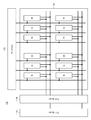
- FIG. 1 is a block diagram of an organic EL display device including an active matrix drive circuit to which the present technology can be applied.
- FIG. 2 is a block diagram showing the configuration of the pixel portion of the organic EL display device.
- FIG. 3 is a connection diagram showing a configuration of a conventional pixel circuit.
- FIG. 4 is a timing chart for explaining the operation of the conventional pixel circuit.
- FIG. 5 is a connection diagram of the first embodiment of the present technology.
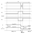
- FIG. 6 is a timing chart for explaining the operation of the first embodiment.
- FIG. 7 is a connection diagram of a modified example of the first embodiment.
- FIG. 8 is a timing chart for explaining the operation of the modified example of the first embodiment.
- FIG. 9 is a connection diagram of the second embodiment of the present technology.
- FIG. 10 is a timing chart for explaining the operation of the second embodiment.
- FIG. 11 is a connection diagram of a modified example of the second embodiment.
- FIG. 12 is a timing chart for explaining the operation of the
- an organic EL display device 10 including an active matrix drive circuit includes a scan line drive circuit 11, a direct current (DC) voltage supply unit 12, and a data line (signal line) drive on a semiconductor substrate such as a silicon substrate.
- the circuit 13 and the pixel portion 14 are formed.
- a plurality of scanning lines from the scanning line drive circuit 11 are extended in the horizontal direction with respect to the pixel portion 14, and a plurality of data lines from the data line drive circuit 13 are extended in the vertical direction.
- a scanning line driving circuit 11a that drives the transistor Tr1 and a scanning line driving circuit 11b that drives the transistor Tr2 in the pixel portion are provided.
- Pixel circuits connected to the data lines extending in the vertical direction and the scanning lines extending in the horizontal direction are arranged in a matrix.
- the pixel circuit is provided with pixel circuits corresponding to pixels of three primary colors, as indicated by R (red), G (green), and blue (B). These three pixels represent one dot of the color image.
- FIG. 3 shows a pixel circuit 14m for one pixel.
- the pixel circuit 14m is connected to the scanning line Xm1 from the scanning line driving circuit 11a, the scanning line Xm2 from the scanning line driving circuit 11b, and the data line Ym from the data line driving circuit 13.
- the anode of the OLED 15 is connected to the source of the drive transistor DrvTr through the source and drain of the transistor Tr4, and the drain of the drive transistor DrvTr is connected to the power supply line that is supplied with the DC voltage VCCP.
- the DC voltage from the DC voltage supply unit 12b is supplied to the gate of the transistor Tr4.
- the source of the drive transistor DrvTr is referred to as an anode node Vanode.
- the OLED 15 is driven by the voltage of the anode node Vanode (gradation of the video signal).
- the gate of the P-channel type transistor Tr1 is connected to the data line Xm1, and the gate of the N-channel type transistor Tr2 is connected to the data line Xm2.
- the sources and the drains D of the transistors Tr1 and Tr2 are connected to each other.
- the signal voltage Vsig is supplied to the common drain connection point through the data line Ym.
- the common source connection point of the transistors Tr1 and Tr2 is connected to the gate of the drive transistor DrvTr.
- a capacitor Cs as a storage capacitor is inserted between the common connection point of these sources, the connection line of the gate of the drive transistor DrvTr, and the power supply line to which the DC voltage VSS is supplied.
- the power supply line to which the DC voltage VSS is supplied is connected to the drain of the transistor Tr3, and the source of the transistor Tr3 is connected to the source of the drive transistor DrvTr.
- the DC voltage from the DC voltage supply unit 12a is supplied to the gate of the transistor Tr3.
- the transistor Tr3 is an anode voltage setting transistor that determines the voltage applied to the anode.
- the capacitor Cs holds the signal voltage Vsig component between the gate of the drive transistor DrvTr and the power supply line to which VSS is supplied.
- FIG. 4 shows a timing chart when the voltage of the conventional pixel circuit 14m is driven.
- This circuit is a voltage drive circuit, and is a system in which the voltage applied to the anode node Vanode is varied according to the signal voltage Vsig to control the emission brightness of the OLED 15 for each gradation. The method of determining the voltage applied to the anode node Vanode is described below.
- the transistors Tr1 and Tr2 are turned on when writing a signal, and the signal voltage Vsig is written.
- the gate voltage of the transistor Tr3 is preferably set to the highest threshold voltage in the panel surface.
- the transistor Tr3 continues to flow a constant current, but an equivalent current also flows to the drive transistor DrvTr, and the gate-source voltage Vgs_Drv of the drive transistor DrvTr becomes a voltage corresponding to the current.
- the source voltage that is, the anode node Vanode is determined as follows.
- Vgs_Drv is the gate-source voltage of the drive transistor DrvTr.
- the anode node Vanode Since the DC voltage is applied to the transistor Tr4 as well as the transistor Tr3, the anode node Vanode is held at the voltage in the above formula. A current corresponding to the voltage of the anode node Vanode flows through the OLED 15, and the OLED emits light with a brightness corresponding to the signal voltage.
- the N-channel transistor Tr3 is always turned on by the DC voltage. This is required to hold the Vanode that determines the emission brightness of the OLED 15.
- the transistor Tr3 since the transistor Tr3 is always turned on, there is a problem that power is always consumed irrespective of the display state of the screen, for example, at the time of full black display.
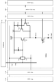
- the pixel portion according to the first embodiment is represented by 141, and the pixel circuit is represented by 141 m.
- the pixel circuit 141m has a configuration in which a second storage capacitor Cs2 and a switching transistor Tr5 are added to the above-described conventional configuration shown in FIG.
- the storage capacitor Cs2 is connected between the gate of the drive transistor DrvTr as the first transistor and the drain of the switching transistor Tr5 as the third transistor, and the source of the switching transistor Tr5 is connected to the source of the drive transistor DrvTr.
- the switching transistor Tr5 may be connected to the gate side of the drive transistor DrvTr and the storage capacitor Cs2 may be connected to the source side thereof.
- the pulse signal from the scan circuit 21 is supplied to the gate of the transistor Tr3, which is connected between the anode node Vanode and the power supply and serves as the second transistor for setting the anode voltage that determines the voltage applied to the anode.
- the DC voltage from the DC voltage supply unit 22 is supplied to the gate of the transistor Tr4.
- a pulse signal from the scan circuit 23 is supplied to the gate of the added switching transistor Tr5.
- the transistors Tr3 and Tr5 are of the same conductivity type (N channel).
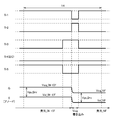
- FIG. 6 shows a timing chart at the time of voltage driving of the pixel circuit 141m according to the first embodiment of the present technology.
- the transistor Tr4 is always turned on by the DC voltage from the DC voltage supply unit 22.
- the transistors Tr1 and Tr2 are turned on when writing a signal.
- the transistor Tr3 is turned on by the pulse signal from the scan circuit 21 at the time of signal writing and near the end of the light emitting period before that. After the signal writing is completed, the transistor Tr3 is turned off and at the same time, the transistor Tr5 is turned on.
- the voltage of the anode node Vanode is held by the holding capacitor Cs2. That is, by supplying the transistor Tr3 with a pulse signal which is turned on at the time of signal writing, the current flowing through the transistor Tr3 flows only to the pixels in the row in which the signal writing is performed. Electric power can be reduced as compared with the conventional configuration in which a DC voltage is applied to the transistor Tr3.
- the pulses that drive the transistors Tr3 and Tr5 have opposite phases, and the influence of charge injection from each transistor on the anode node Vanode can be canceled. Therefore, the anode node Vanode can be held accurately (Vsig-Vgs_Drv).
- FIG. 7 shows a configuration of a modified example of the first embodiment.
- the switching transistor Tr5 is changed to a P-channel type switching transistor Tr6.
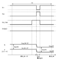
- FIG. 8 shows a timing chart at the time of voltage driving of the modified example.
- the transistor Tr3 and the switching transistor Tr6 have different conductivity types (N-channel type and P-channel type), the transistor Tr3 can be turned on and the switching transistor Tr6 can be turned on by a pulse signal of the same polarity. it can. Therefore, since the common scan circuit 24 may be provided for the transistor Tr3 and the switching transistor Tr6, the number of scan circuits can be reduced by one.
- the pixel portion according to the second embodiment is represented by 142, and the pixel circuit is represented by 142m.
- the pixel circuit 142m has a configuration in which a second storage capacitor Cs2 and a switching transistor Tr5 are added to the above-described conventional configuration shown in FIG.
- the source of the switching transistor Tr5 is connected to the source of the drive transistor DrvTr, and the second storage capacitor Cs2 is connected between the drain of the switching transistor Tr5 and the power supply line to which the fixed power supply, for example, the DC voltage VSS is supplied.
- the connection order of the switching transistor Tr5 and the storage capacitor Cs2 may be exchanged.
- FIG. 10 shows a timing chart when driving the voltage of the pixel circuit 142m according to the second embodiment of the present technology. It is similar to the timing chart showing the operation of the first embodiment. That is, the transistor Tr4 is always turned on by the DC voltage from the DC voltage supply unit 22. The transistors Tr1 and Tr2 are turned on when writing a signal. Further, the scan circuits 21 and 23 supply pulse signals of opposite phases to the transistor Tr3 and the switching transistor Tr5.
- the current flowing in the transistor Tr3 flows only in the pixels in the row in which signal writing is performed. Electric power can be reduced as compared with the conventional configuration in which a DC voltage is applied to the transistor Tr3. Further, the pulses for driving the transistors Tr3 and Tr5 have opposite phases, and the influence of charge injection from each transistor on the anode node Vanode can be canceled.
- FIG. 11 shows a configuration of a modified example of the second embodiment.
- the switching transistor Tr5 is replaced with a switching transistor Tr6 of a conductivity type (P-channel type) different from that of the transistor Tr3.
- FIG. 12 shows a timing chart at the time of voltage driving.
- the transistor Tr3 and the switching transistor Tr6 are the N-channel type and the P-channel type, it is possible to switch the transistor Tr3 from off to on and the switching transistor Tr6 from on to off by a pulse signal of the same polarity. Therefore, since the common scan circuit 24 may be provided for the transistor Tr3 and the switching transistor Tr6, the number of scan circuits can be reduced by one.
- the transistors Tr1 and Tr2 are provided to apply the signal voltage to the gate of the drive transistor DrvTr, but only one transistor may be provided.
- an OLED that is a light emitting element is illustrated as an electro-optical element, but an inorganic light emitting diode, an LED (Light Emitting Diode), or the like may be used as long as it emits light with a luminance according to a current.
- the electro-optical device is suitable for applications in which the pixel has a small size and high-definition display. Therefore, the electronic device can be applied to a display device such as a head mounted display, smart glasses, a smartphone, an electronic viewfinder of a digital camera.
- a display device such as a head mounted display, smart glasses, a smartphone, an electronic viewfinder of a digital camera.
- an electro-optical device including an active matrix type drive circuit for applying a voltage according to a video signal gradation to a light emitting element, A first transistor for driving whose source is connected to the anode of the light emitting device; A second transistor connected between the anode and a power supply for setting an anode voltage for determining a voltage applied to the anode; An electro-optical device comprising: a storage capacitor connected to the anode and a third transistor for holding an anode voltage during a light emission period.
- the electro-optical device according to (1) wherein the second transistor is turned on during a signal writing period, and then the third transistor is turned on to hold the anode voltage.
- the electro-optical device according to (1) is provided, Electronics.
- 11a, 11b ... Scanning line driving circuit, 13... Data line (signal line) driving circuit, 15... OLED, 21, 23... Scan circuit, 22... DC voltage supply unit, DrvTr ⁇ Drive transistor
Landscapes
- Engineering & Computer Science (AREA)
- Physics & Mathematics (AREA)
- Computer Hardware Design (AREA)
- General Physics & Mathematics (AREA)
- Theoretical Computer Science (AREA)
- Microelectronics & Electronic Packaging (AREA)
- Geometry (AREA)
- Control Of Indicators Other Than Cathode Ray Tubes (AREA)
- Control Of El Displays (AREA)
- Electroluminescent Light Sources (AREA)
Abstract
Description
ソースが発光素子のアノードに接続されたドライブ用の第1のトランジスタと、
アノードと電源の間に接続され、アノードに印加する電圧を決定するアノード電圧設定用の第2のトランジスタと、
発光期間中にアノード電圧を保持するために、アノードに接続された保持容量及び第3のトランジスタと
を備える電気光学装置である。
また、本技術は、かかる電気光学装置を備える電子機器である。
Vsig -Vgs_Drv
(1)
映像信号階調に応じた電圧を発光素子に対して印加するアクティブマトリクス型駆動回路を備える電気光学装置において、
ソースが前記発光素子のアノードに接続されたドライブ用の第1のトランジスタと、
前記アノードと電源の間に接続され、前記アノードに印加する電圧を決定するアノード電圧設定用の第2のトランジスタと、
発光期間中にアノード電圧を保持するために、前記アノードに接続された保持容量及び第3のトランジスタと
を備える電気光学装置。
(2)
前記第2のトランジスタは、信号書き込み期間でオンし、その後前記第3のトランジスタをオンして前記アノード電圧をホールドするようにした(1)に記載の電気光学装置。
(3)
前記保持容量及び前記第3のトランジスタが前記ドライブ用の第1のトランジスタのゲート及びソース間に接続された(1)又は(2)に記載の電気光学装置。
(4)
前記保持容量及び前記第3のトランジスタが前記ドライブ用の第1のトランジスタのソース及び直流電位の供給箇所に接続された(1)から(3)のいずれかに記載の電気光学装置。
(5)
前記第2のトランジスタ及び前記第3のトランジスタが異なる導電型とされた(1)から(4)のいずれかに記載の電気光学装置。
(6)
前記第2のトランジスタ及び前記第3のトランジスタが同じ導電型とされた(1)から(4)のいずれかに記載の電気光学装置。
(7)
(1)に記載の電気光学装置を備える、
電子機器。
(8)
前記電気光学装置において、
前記第2のトランジスタは、信号書き込み期間でオンし、その後前記第3のトランジスタをオンして前記アノード電位をホールドするようにした(7)に記載の電子機器。
15・・・OLED、21,23・・・スキャン回路、22・・・直流電圧供給部、
DrvTr・・・ドライブトランジスタ
Claims (8)
- 映像信号階調に応じた電圧を発光素子に対して印加するアクティブマトリクス型駆動回路を備える電気光学装置において、
ソースが前記発光素子のアノードに接続されたドライブ用の第1のトランジスタと、
前記アノードと電源の間に接続され、前記アノードに印加する電圧を決定するアノード電圧設定用の第2のトランジスタと、
発光期間中にアノード電圧を保持するために、前記アノードに接続された保持容量及び第3のトランジスタと
を備える電気光学装置。 - 前記第2のトランジスタは、信号書き込み期間でオンし、その後前記第3のトランジスタをオンして前記アノード電圧をホールドするようにした請求項1に記載の電気光学装置。
- 前記保持容量及び前記第3のトランジスタが前記ドライブ用の第1のトランジスタのゲート及びソース間に接続された請求項1に記載の電気光学装置。
- 前記保持容量及び前記第3のトランジスタが前記ドライブ用の第1のトランジスタのソース及び直流電位の供給箇所に接続された請求項1に記載の電気光学装置。
- 前記第2のトランジスタ及び前記第3のトランジスタが異なる導電型とされた請求項1に記載の電気光学装置。
- 前記第2のトランジスタ及び前記第3のトランジスタが同じ導電型とされた請求項1に記載の電気光学装置。
- 請求項1に記載の電気光学装置を備える、
電子機器。 - 前記電気光学装置において、
前記第2のトランジスタは、信号書き込み期間でオンし、その後前記第3のトランジスタをオンして前記アノード電位をホールドするようにした請求項7に記載の電子機器。
Priority Applications (5)
| Application Number | Priority Date | Filing Date | Title |
|---|---|---|---|
| DE112019006661.7T DE112019006661T5 (de) | 2019-01-16 | 2019-10-17 | Elektrooptische vorrichtung und elektronisches gerät |
| KR1020217018300A KR102816711B1 (ko) | 2019-01-16 | 2019-10-17 | 전기 광학 장치 및 전자 기기 |
| JP2020566108A JPWO2020148958A1 (ja) | 2019-01-16 | 2019-10-17 | 電気光学装置及び電子機器 |
| US17/420,792 US12136395B2 (en) | 2019-01-16 | 2019-10-17 | Electro-optical apparatus and electronic device including a transistor for applying a voltage to an anode of a light emitting element |
| CN201980077357.0A CN113168813B (zh) | 2019-01-16 | 2019-10-17 | 电光装置和电子设备 |
Applications Claiming Priority (2)
| Application Number | Priority Date | Filing Date | Title |
|---|---|---|---|
| JP2019005409 | 2019-01-16 | ||
| JP2019-005409 | 2019-01-16 |
Publications (1)
| Publication Number | Publication Date |
|---|---|
| WO2020148958A1 true WO2020148958A1 (ja) | 2020-07-23 |
Family
ID=71614506
Family Applications (1)
| Application Number | Title | Priority Date | Filing Date |
|---|---|---|---|
| PCT/JP2019/040812 Ceased WO2020148958A1 (ja) | 2019-01-16 | 2019-10-17 | 電気光学装置及び電子機器 |
Country Status (6)
| Country | Link |
|---|---|
| US (1) | US12136395B2 (ja) |
| JP (1) | JPWO2020148958A1 (ja) |
| KR (1) | KR102816711B1 (ja) |
| CN (1) | CN113168813B (ja) |
| DE (1) | DE112019006661T5 (ja) |
| WO (1) | WO2020148958A1 (ja) |
Families Citing this family (1)
| Publication number | Priority date | Publication date | Assignee | Title |
|---|---|---|---|---|
| CN110288950B (zh) * | 2019-08-06 | 2022-03-25 | 京东方科技集团股份有限公司 | 像素阵列、阵列基板及显示装置 |
Citations (5)
| Publication number | Priority date | Publication date | Assignee | Title |
|---|---|---|---|---|
| JP2005534990A (ja) * | 2002-08-06 | 2005-11-17 | コーニンクレッカ フィリップス エレクトロニクス エヌ ヴィ | Nmosトランジスタを備えたピクセルを持つエレクトロルミネセントディスプレイ装置 |
| JP2008191450A (ja) * | 2007-02-06 | 2008-08-21 | Seiko Epson Corp | 画素回路、画素回路の駆動方法、電気光学装置および電子機器 |
| JP2015188059A (ja) * | 2013-12-27 | 2015-10-29 | 株式会社半導体エネルギー研究所 | 発光装置 |
| WO2015196730A1 (zh) * | 2014-06-23 | 2015-12-30 | 京东方科技集团股份有限公司 | 像素电路及其驱动方法和显示装置 |
| US20170278457A1 (en) * | 2017-01-23 | 2017-09-28 | Shanghai Tianma AM-OLED Co., Ltd. | Organic Light-Emitting Pixel Driving Circuit, Driving Method And Organic Light-Emitting Display Device |
Family Cites Families (16)
| Publication number | Priority date | Publication date | Assignee | Title |
|---|---|---|---|---|
| KR100962961B1 (ko) * | 2008-06-17 | 2010-06-10 | 삼성모바일디스플레이주식회사 | 화소 및 이를 이용한 유기전계발광 표시장치 |
| US8766883B2 (en) | 2009-08-20 | 2014-07-01 | Emagin Corporation | Dual-mode AMOLED pixel driver, a system using a dual-mode AMOLED pixel driver, and a method of operating a dual-mode AMOLED pixel driver |
| KR101839533B1 (ko) * | 2010-12-28 | 2018-03-19 | 삼성디스플레이 주식회사 | 유기 발광 표시 장치, 이의 구동 방법 및 그 제조 방법 |
| KR101842721B1 (ko) * | 2011-08-09 | 2018-03-27 | 가부시키가이샤 제이올레드 | 표시장치 |
| JP6079312B2 (ja) * | 2013-03-04 | 2017-02-15 | セイコーエプソン株式会社 | 電気光学装置、電子機器、及び電気光学装置の駆動方法 |
| JP2015045830A (ja) | 2013-08-29 | 2015-03-12 | 三星ディスプレイ株式會社Samsung Display Co.,Ltd. | 電気光学装置 |
| CN104575372B (zh) * | 2013-10-25 | 2016-10-12 | 京东方科技集团股份有限公司 | 一种amoled像素驱动电路及其驱动方法、阵列基板 |
| KR102193782B1 (ko) * | 2014-06-10 | 2020-12-23 | 삼성디스플레이 주식회사 | 화소 및 이를 이용한 유기전계발광 표시장치 |
| CN104809989A (zh) | 2015-05-22 | 2015-07-29 | 京东方科技集团股份有限公司 | 一种像素电路、其驱动方法及相关装置 |
| KR102389343B1 (ko) * | 2015-08-27 | 2022-04-25 | 삼성디스플레이 주식회사 | 화소, 화소를 포함하는 유기전계발광 표시장치 및 화소의 구동 방법 |
| CN105047138B (zh) * | 2015-09-15 | 2018-01-05 | 深圳市华星光电技术有限公司 | 一种显示装置的驱动系统及适用于oled的驱动电路 |
| KR102665322B1 (ko) * | 2016-06-24 | 2024-05-16 | 삼성디스플레이 주식회사 | 박막 트랜지스터 기판, 및 표시 장치 |
| CN106782304B (zh) * | 2016-12-29 | 2023-11-17 | 上海天马微电子有限公司 | 一种像素驱动电路、像素阵列、驱动方法及有机发光显示面板 |
| CN107025883B (zh) * | 2017-04-28 | 2019-05-03 | 深圳市华星光电半导体显示技术有限公司 | 显示面板、像素驱动电路及其驱动方法 |
| CN107039002B (zh) * | 2017-06-05 | 2019-09-06 | 京东方科技集团股份有限公司 | 一种像素电路及显示面板 |
| CN107424570B (zh) * | 2017-08-11 | 2022-07-01 | 京东方科技集团股份有限公司 | 像素单元电路、像素电路、驱动方法和显示装置 |
-
2019
- 2019-10-17 DE DE112019006661.7T patent/DE112019006661T5/de active Pending
- 2019-10-17 KR KR1020217018300A patent/KR102816711B1/ko active Active
- 2019-10-17 JP JP2020566108A patent/JPWO2020148958A1/ja active Pending
- 2019-10-17 US US17/420,792 patent/US12136395B2/en active Active
- 2019-10-17 CN CN201980077357.0A patent/CN113168813B/zh active Active
- 2019-10-17 WO PCT/JP2019/040812 patent/WO2020148958A1/ja not_active Ceased
Patent Citations (5)
| Publication number | Priority date | Publication date | Assignee | Title |
|---|---|---|---|---|
| JP2005534990A (ja) * | 2002-08-06 | 2005-11-17 | コーニンクレッカ フィリップス エレクトロニクス エヌ ヴィ | Nmosトランジスタを備えたピクセルを持つエレクトロルミネセントディスプレイ装置 |
| JP2008191450A (ja) * | 2007-02-06 | 2008-08-21 | Seiko Epson Corp | 画素回路、画素回路の駆動方法、電気光学装置および電子機器 |
| JP2015188059A (ja) * | 2013-12-27 | 2015-10-29 | 株式会社半導体エネルギー研究所 | 発光装置 |
| WO2015196730A1 (zh) * | 2014-06-23 | 2015-12-30 | 京东方科技集团股份有限公司 | 像素电路及其驱动方法和显示装置 |
| US20170278457A1 (en) * | 2017-01-23 | 2017-09-28 | Shanghai Tianma AM-OLED Co., Ltd. | Organic Light-Emitting Pixel Driving Circuit, Driving Method And Organic Light-Emitting Display Device |
Also Published As
| Publication number | Publication date |
|---|---|
| CN113168813B (zh) | 2025-01-03 |
| KR102816711B1 (ko) | 2025-06-05 |
| US12136395B2 (en) | 2024-11-05 |
| KR20210114389A (ko) | 2021-09-23 |
| JPWO2020148958A1 (ja) | 2021-12-02 |
| CN113168813A (zh) | 2021-07-23 |
| US20220114965A1 (en) | 2022-04-14 |
| DE112019006661T5 (de) | 2021-12-09 |
Similar Documents
| Publication | Publication Date | Title |
|---|---|---|
| US20230119752A1 (en) | Pixel, organic light emitting display device using the same, and method of driving the organic light emitting display device | |
| CN113053281B (zh) | 像素驱动电路以及包括像素驱动电路的电致发光显示装置 | |
| CN112992049B (zh) | 具有像素驱动电路的电致发光显示装置 | |
| KR101087417B1 (ko) | 유기 발광표시장치의 구동회로 | |
| JP5611312B2 (ja) | 有機発光ダイオード表示装置及びその駆動方法 | |
| JP5612988B2 (ja) | 有機電界発光表示装置用画素及びこれを利用した有機電界発光表示装置 | |
| CN103700338B (zh) | 像素电路及其驱动方法及采用该电路的有机发光显示装置 | |
| KR101399159B1 (ko) | 유기발광 표시장치 | |
| CN108510936A (zh) | 电致发光显示装置 | |
| US20080252217A1 (en) | Pixel, organic light emitting display using the same, and associated methods | |
| KR20190142791A (ko) | 표시 장치 | |
| KR20210086331A (ko) | 전계 발광 표시 장치 | |
| US20210193055A1 (en) | Organic Light Emitting Display Device and Driving Method for the Same | |
| KR102485163B1 (ko) | 표시장치 | |
| US11881170B2 (en) | Light emitting display device and driving method thereof | |
| KR20140025781A (ko) | 유기 발광 표시장치 | |
| KR102062875B1 (ko) | 화소 및 이를 이용한 유기전계발광 표시장치 | |
| KR20180011397A (ko) | 유기발광 표시장치와 그 구동방법 | |
| KR20150025538A (ko) | 유기전계발광 표시장치 및 그의 구동방법 | |
| KR102652623B1 (ko) | Oled 표시 장치의 구동 방법 | |
| KR20190079827A (ko) | 구동 전압 라인 없는 화소 회로 및 이 화소 회로를 사용하는 유기발광 표시장치 | |
| KR101907959B1 (ko) | 유기 발광 다이오드 표시장치 | |
| CN113168813B (zh) | 电光装置和电子设备 | |
| KR20150010064A (ko) | 유기전계발광 표시장치 | |
| KR101348406B1 (ko) | 구동회로 및 이를 포함하는 유기 이엘 디스플레이 장치 |
Legal Events
| Date | Code | Title | Description |
|---|---|---|---|
| 121 | Ep: the epo has been informed by wipo that ep was designated in this application |
Ref document number: 19910616 Country of ref document: EP Kind code of ref document: A1 |
|
| ENP | Entry into the national phase |
Ref document number: 2020566108 Country of ref document: JP Kind code of ref document: A |
|
| 122 | Ep: pct application non-entry in european phase |
Ref document number: 19910616 Country of ref document: EP Kind code of ref document: A1 |
|
| WWG | Wipo information: grant in national office |
Ref document number: 201980077357.0 Country of ref document: CN |