WO2020129436A1 - 半導体装置 - Google Patents
半導体装置 Download PDFInfo
- Publication number
- WO2020129436A1 WO2020129436A1 PCT/JP2019/043167 JP2019043167W WO2020129436A1 WO 2020129436 A1 WO2020129436 A1 WO 2020129436A1 JP 2019043167 W JP2019043167 W JP 2019043167W WO 2020129436 A1 WO2020129436 A1 WO 2020129436A1
- Authority
- WO
- WIPO (PCT)
- Prior art keywords
- gate
- region
- sense
- gate electrode
- electrode layer
- Prior art date
- Legal status (The legal status is an assumption and is not a legal conclusion. Google has not performed a legal analysis and makes no representation as to the accuracy of the status listed.)
- Ceased
Links
Images










Classifications
-
- H—ELECTRICITY
- H10—SEMICONDUCTOR DEVICES; ELECTRIC SOLID-STATE DEVICES NOT OTHERWISE PROVIDED FOR
- H10D—INORGANIC ELECTRIC SEMICONDUCTOR DEVICES
- H10D84/00—Integrated devices formed in or on semiconductor substrates that comprise only semiconducting layers, e.g. on Si wafers or on GaAs-on-Si wafers
- H10D84/80—Integrated devices formed in or on semiconductor substrates that comprise only semiconducting layers, e.g. on Si wafers or on GaAs-on-Si wafers characterised by the integration of at least one component covered by groups H10D12/00 or H10D30/00, e.g. integration of IGFETs
- H10D84/811—Combinations of field-effect devices and one or more diodes, capacitors or resistors
- H10D84/817—Combinations of field-effect devices and resistors only
-
- H—ELECTRICITY
- H10—SEMICONDUCTOR DEVICES; ELECTRIC SOLID-STATE DEVICES NOT OTHERWISE PROVIDED FOR
- H10D—INORGANIC ELECTRIC SEMICONDUCTOR DEVICES
- H10D12/00—Bipolar devices controlled by the field effect, e.g. insulated-gate bipolar transistors [IGBT]
- H10D12/411—Insulated-gate bipolar transistors [IGBT]
- H10D12/441—Vertical IGBTs
- H10D12/461—Vertical IGBTs having non-planar surfaces, e.g. having trenches, recesses or pillars in the surfaces of the emitter, base or collector regions
- H10D12/481—Vertical IGBTs having non-planar surfaces, e.g. having trenches, recesses or pillars in the surfaces of the emitter, base or collector regions having gate structures on slanted surfaces, on vertical surfaces, or in grooves, e.g. trench gate IGBTs
-
- H—ELECTRICITY
- H10—SEMICONDUCTOR DEVICES; ELECTRIC SOLID-STATE DEVICES NOT OTHERWISE PROVIDED FOR
- H10D—INORGANIC ELECTRIC SEMICONDUCTOR DEVICES
- H10D62/00—Semiconductor bodies, or regions thereof, of devices having potential barriers
- H10D62/10—Shapes, relative sizes or dispositions of the regions of the semiconductor bodies; Shapes of the semiconductor bodies
- H10D62/124—Shapes, relative sizes or dispositions of the regions of semiconductor bodies or of junctions between the regions
- H10D62/126—Top-view geometrical layouts of the regions or the junctions
- H10D62/127—Top-view geometrical layouts of the regions or the junctions of cellular field-effect devices, e.g. multicellular DMOS transistors or IGBTs
-
- H—ELECTRICITY
- H10—SEMICONDUCTOR DEVICES; ELECTRIC SOLID-STATE DEVICES NOT OTHERWISE PROVIDED FOR
- H10D—INORGANIC ELECTRIC SEMICONDUCTOR DEVICES
- H10D64/00—Electrodes of devices having potential barriers
- H10D64/20—Electrodes characterised by their shapes, relative sizes or dispositions
- H10D64/27—Electrodes not carrying the current to be rectified, amplified, oscillated or switched, e.g. gates
- H10D64/311—Gate electrodes for field-effect devices
- H10D64/411—Gate electrodes for field-effect devices for FETs
- H10D64/511—Gate electrodes for field-effect devices for FETs for IGFETs
- H10D64/512—Disposition of the gate electrodes, e.g. buried gates
- H10D64/513—Disposition of the gate electrodes, e.g. buried gates within recesses in the substrate, e.g. trench gates, groove gates or buried gates
-
- H—ELECTRICITY
- H10—SEMICONDUCTOR DEVICES; ELECTRIC SOLID-STATE DEVICES NOT OTHERWISE PROVIDED FOR
- H10D—INORGANIC ELECTRIC SEMICONDUCTOR DEVICES
- H10D64/00—Electrodes of devices having potential barriers
- H10D64/20—Electrodes characterised by their shapes, relative sizes or dispositions
- H10D64/27—Electrodes not carrying the current to be rectified, amplified, oscillated or switched, e.g. gates
- H10D64/311—Gate electrodes for field-effect devices
- H10D64/411—Gate electrodes for field-effect devices for FETs
- H10D64/511—Gate electrodes for field-effect devices for FETs for IGFETs
- H10D64/517—Gate electrodes for field-effect devices for FETs for IGFETs characterised by the conducting layers
- H10D64/519—Gate electrodes for field-effect devices for FETs for IGFETs characterised by the conducting layers characterised by their top-view geometrical layouts
-
- H—ELECTRICITY
- H10—SEMICONDUCTOR DEVICES; ELECTRIC SOLID-STATE DEVICES NOT OTHERWISE PROVIDED FOR
- H10D—INORGANIC ELECTRIC SEMICONDUCTOR DEVICES
- H10D89/00—Aspects of integrated devices not covered by groups H10D84/00 - H10D88/00
- H10D89/60—Integrated devices comprising arrangements for electrical or thermal protection, e.g. protection circuits against electrostatic discharge [ESD]
-
- H—ELECTRICITY
- H10—SEMICONDUCTOR DEVICES; ELECTRIC SOLID-STATE DEVICES NOT OTHERWISE PROVIDED FOR
- H10D—INORGANIC ELECTRIC SEMICONDUCTOR DEVICES
- H10D1/00—Resistors, capacitors or inductors
- H10D1/40—Resistors
- H10D1/47—Resistors having no potential barriers
-
- H—ELECTRICITY
- H10—SEMICONDUCTOR DEVICES; ELECTRIC SOLID-STATE DEVICES NOT OTHERWISE PROVIDED FOR
- H10D—INORGANIC ELECTRIC SEMICONDUCTOR DEVICES
- H10D84/00—Integrated devices formed in or on semiconductor substrates that comprise only semiconducting layers, e.g. on Si wafers or on GaAs-on-Si wafers
- H10D84/01—Manufacture or treatment
- H10D84/0123—Integrating together multiple components covered by H10D12/00 or H10D30/00, e.g. integrating multiple IGBTs
- H10D84/0126—Integrating together multiple components covered by H10D12/00 or H10D30/00, e.g. integrating multiple IGBTs the components including insulated gates, e.g. IGFETs
- H10D84/016—Integrating together multiple components covered by H10D12/00 or H10D30/00, e.g. integrating multiple IGBTs the components including insulated gates, e.g. IGFETs the components including vertical IGFETs
-
- H—ELECTRICITY
- H10—SEMICONDUCTOR DEVICES; ELECTRIC SOLID-STATE DEVICES NOT OTHERWISE PROVIDED FOR
- H10D—INORGANIC ELECTRIC SEMICONDUCTOR DEVICES
- H10D84/00—Integrated devices formed in or on semiconductor substrates that comprise only semiconducting layers, e.g. on Si wafers or on GaAs-on-Si wafers
- H10D84/01—Manufacture or treatment
- H10D84/02—Manufacture or treatment characterised by using material-based technologies
- H10D84/03—Manufacture or treatment characterised by using material-based technologies using Group IV technology, e.g. silicon technology or silicon-carbide [SiC] technology
- H10D84/038—Manufacture or treatment characterised by using material-based technologies using Group IV technology, e.g. silicon technology or silicon-carbide [SiC] technology using silicon technology, e.g. SiGe
-
- H—ELECTRICITY
- H10—SEMICONDUCTOR DEVICES; ELECTRIC SOLID-STATE DEVICES NOT OTHERWISE PROVIDED FOR
- H10D—INORGANIC ELECTRIC SEMICONDUCTOR DEVICES
- H10D89/00—Aspects of integrated devices not covered by groups H10D84/00 - H10D88/00
- H10D89/10—Integrated device layouts
-
- H—ELECTRICITY
- H10—SEMICONDUCTOR DEVICES; ELECTRIC SOLID-STATE DEVICES NOT OTHERWISE PROVIDED FOR
- H10W—GENERIC PACKAGES, INTERCONNECTIONS, CONNECTORS OR OTHER CONSTRUCTIONAL DETAILS OF DEVICES COVERED BY CLASS H10
- H10W10/00—Isolation regions in semiconductor bodies between components of integrated devices
- H10W10/01—Manufacture or treatment
- H10W10/031—Manufacture or treatment of isolation regions comprising PN junctions
-
- H—ELECTRICITY
- H10—SEMICONDUCTOR DEVICES; ELECTRIC SOLID-STATE DEVICES NOT OTHERWISE PROVIDED FOR
- H10W—GENERIC PACKAGES, INTERCONNECTIONS, CONNECTORS OR OTHER CONSTRUCTIONAL DETAILS OF DEVICES COVERED BY CLASS H10
- H10W10/00—Isolation regions in semiconductor bodies between components of integrated devices
- H10W10/30—Isolation regions comprising PN junctions
-
- H—ELECTRICITY
- H10—SEMICONDUCTOR DEVICES; ELECTRIC SOLID-STATE DEVICES NOT OTHERWISE PROVIDED FOR
- H10W—GENERIC PACKAGES, INTERCONNECTIONS, CONNECTORS OR OTHER CONSTRUCTIONAL DETAILS OF DEVICES COVERED BY CLASS H10
- H10W72/00—Interconnections or connectors in packages
- H10W72/90—Bond pads, in general
- H10W72/921—Structures or relative sizes of bond pads
- H10W72/926—Multiple bond pads having different sizes
Definitions
- the present invention relates to a semiconductor device.
- an IPM Intelligent Power Module
- main IGBT Insulated Gate Bipolar Transistor
- OC Over Current
- the current sensing unit is an IGBT (hereinafter, a few thousandths of the number of unit cells of the main IGBT) provided with a smaller number of unit cells (functional units of elements) having the same configuration as the main IGBT (for example, a unit cell of the main IGBT) (hereinafter, Sense IGBT).
- the sense IGBT is arranged in a predetermined region of the same semiconductor substrate as the main IGBT and is connected in parallel to the main IGBT.
- the collector-emitter current flowing through the sense IGBT is determined according to the ratio of the number of unit cells of the main IGBT and the sense IGBT, and has a smaller amount of current than the collector-emitter current flowing through the main IGBT.
- the collector-emitter current flowing through the sense IGBT is detected by a control IC (Integrated Circuit) that is connected to the main electrode of the sense IGBT via a wire.
- the control IC determines whether or not an overcurrent is flowing between the collector and emitter of the main IGBT, based on the amount of collector-emitter current flowing through the sense IGBT.
- the control IC turns off the gate of the main IGBT to stop the operation of the main IGBT, thereby shutting off the current between the collector and the emitter of the main IGBT. Has a protective function.
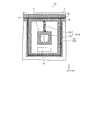
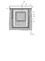
- FIG. 28 is a plan view showing a layout of a conventional semiconductor device viewed from the front surface side of a semiconductor substrate.
- 29 and 30 are plan views showing the vicinity of the current sensing portion of FIG. 28 in an enlarged manner.
- the contact hole 145 between the gate runner metal and the gate runner 115 and the contact hole 146 between the extended portion of the gate runner metal and the extended portion 116 of the gate runner 115 are indicated by thick lines.
- FIG. 31 is a sectional view showing a sectional structure taken along the section line AA-AA′ in FIGS.
- the conventional semiconductor device 110 shown in FIGS. 28 to 31 includes a semiconductor substrate (semiconductor chip) 107, a main IGBT 120, and a sense IGBT 130 as a current sense unit for detecting a current flowing through the main IGBT 120.
- the main IGBT 120 and the sense IGBT 130 are trench gate type IGBTs having the same structure.
- the semiconductor substrate 107 is provided with an active region 101 having the first and second cell regions 102 and 103, and an edge termination region 106 surrounding the active region 101.
- a p + type region (hereinafter referred to as a p + type isolation region) 141 is arranged inside the semiconductor substrate 107 so as to surround the first cell region 102.
- the unit cell of the main IGBT 120 is arranged in a region surrounded by the p + type isolation region 141 in the first cell region 102.
- the first cell region 102 is separated from the regions other than the first cell region 102 by the pn junction between the p + type isolation region 141 and the n ⁇ type drift region 121.
- the first cell region 102 is a portion of the active region 101 excluding the second cell region 103, and occupies most of the surface area of the active region 101.
- the emitter electrode 151 of the main IGBT 120 is provided on the front surface of the semiconductor substrate 107.
- the emitter electrode 151 of the main IGBT 120 covers almost the entire first cell region 102.
- a part of the emitter electrode 151 constitutes the emitter pad 111.
- a gate pad 112 is arranged near the boundary between the first cell region 102 and the edge termination region 106.
- the gate pad 112 is connected to the gate runner 115.
- a unit cell of the sense IGBT 130 is arranged in the second cell region 103.
- the second cell region 103 has a detection region 104 in which the unit cells of the sense IGBT 130 are arranged and a drawing region 105 for drawing a hole current.
- p + type isolation regions 141 and 142 are selectively provided inside the semiconductor substrate 107.
- the p + type isolation region 141 surrounds the periphery of the detection region 104.
- p + -type isolation region 142, between the detection region 104 and the p + -type isolation region 141 is spaced apart from the p + -type isolation region 141, surrounding the periphery of the detection region 104.
- the detection region 104 of the second cell region 103 is separated from the region other than the detection region 104 by the pn junction between the p + type separation region 142 and the n ⁇ type drift region 121.
- the sense polysilicon layer 113 is arranged on the front surface of the semiconductor substrate 107 via the field oxide film 143.
- the sense polysilicon layer 113 surrounds the periphery of the detection region 104.
- the sense polysilicon layer 113 also serves as the extending portion 116 of the gate runner 115 described later.
- the capacitance formed by the sense polysilicon layer 113, the interlayer insulating film 144, and the emitter electrode 152 of the sense IGBT 130 becomes a part of the gate-emitter capacitance CGE of the sense IGBT 130.
- the emitter electrode 152 of the sense IGBT 130 is provided over almost the entire second cell region 103, and extends on the sense polysilicon layer 113 with the interlayer insulating film 144 interposed therebetween.
- a sense emitter pad 114 formed by a part of the emitter electrode 152 is arranged in the extraction region 105.
- a gate runner 115 made of polysilicon is arranged in the edge termination region 106 and surrounds the periphery of the active region 101.
- the gate runner 115 has a portion (hereinafter referred to as an extension portion) 116 that extends to the second cell region 103 along the outer periphery of the second cell region 103.
- the extending portion 116 of the gate runner 115 surrounds the periphery of the second cell region 103.
- One polysilicon layer formed by the gate runner 115 and the extension portion 116 of the gate runner 115 extends along the outer periphery of the first cell region 102 and surrounds the periphery of the first cell region 102.
- the inner circumference of the sense polysilicon layer 113 (the end portion on the detection region 104 side) is shown by a broken line with a reference numeral 113a.
- the inner circumference (end on the active area 101 side) and the outer circumference (end on the end side of the semiconductor substrate 107) of the portion of the gate runner 115 surrounding the periphery of the active area 101 are indicated by dashed lines 115a and 115b, respectively. Indicate.
- a reference numeral 116a is attached to an end portion of the extending portion 116 of the gate runner 115 on the active region 101 side.
- the sense polysilicon layer 113 is formed integrally with the gate runner 115 and the extending portion 116 of the gate runner 115.
- the gate runner 115 is electrically connected to the gate metal runner 153 via a contact hole 146 formed in the interlayer insulating film 144.
- Gate electrodes 128 and 138 of the main IGBT 120 and the sense IGBT 130 are electrically connected to the gate runner 115.
- an emitter contact trench that penetrates the emitter region and the base region and reaches the drift region is provided between the gate trenches in which the gate electrode is embedded, and the emitter contact trench is embedded inside the trench.
- a trench gate type IGBT in which an emitter electrode and a semiconductor portion are electrically connected via a conductive layer (for example, refer to Patent Document 2 below).
- the effective gate width is smaller than that of a trench gate type IGBT that does not include a trench for emitter contact, and therefore the amount of collector-emitter current of the IGBT is small and the saturation current is suppressed.
- electrostatic discharge Electro
- conductive objects human body and parts, or parts.
- -Static Discharge occurs. Since the sense IGBT 130 occupies a small area with respect to the surface area of the semiconductor substrate 107, the gate-emitter capacitance CGE is very small and the ESD resistance is low. Therefore, when a gate voltage Vg (for example, about 80 V) higher than the breakdown voltage between the gate and the emitter is applied to the sense IGBT 130, the gate insulating film 137 in the gate trench 136 of the sense IGBT 130 is dielectrically broken down.
- Vg for example, about 80 V
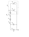
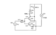
- FIG. 24 is an equivalent circuit diagram showing a switching circuit.
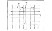
- FIG. 25 is an explanatory diagram showing the result of simulating the current/voltage waveform of the conventional semiconductor device.
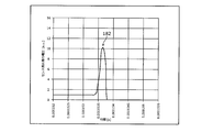
- FIG. 26 is an explanatory diagram showing the result of simulating the voltage waveform of the sense voltage applied to the sense resistor of FIG.
- the horizontal axes of FIGS. 25 and 26 show the same elapsed time.
- the switching circuit shown in FIG. 24 includes a main IGBT 120 and a sense IGBT 130 connected in parallel, and a sense resistor 161.
- One end of the sense resistor 161 is connected to the emitter of the sense IGBT 130.
- the other end of the sense resistor 161 is connected to the emitter of the main IGBT 120.
- the other end of the sense resistor 161 is connected to the gate of the main IGBT 120 and the gate of the sense IGBT 130 via the gate voltage source 166.
- the collector of the main IGBT 120 and the collector of the sense IGBT 130 are connected to the positive electrode of the bus voltage source 163 via the load inductance 162 of the load L1.
- the negative electrode of the bus voltage source 163 is connected to the emitter of the main IGBT 120 and the emitter of the sense IGBT 130.
- a diode 164 is connected in antiparallel to the load inductance 162 between the collector and emitter of the main IGBT 120 and between the collector and emitter of the sense IGBT 130.
- the diode 164 has a function of circulating the current flowing through the collectors of the IGBTs 120 and 130 when the main IGBT 120 and the sense IGBT 130 are turned off.
- An inductive load 165 that assumes the inductance L2 of the wiring is connected between the diode 164 and the collector of the main IGBT 120 and the collector of the sense IGBT 130.
- the gate voltage Vg is applied from the gate voltage source 166 to each gate of the main IGBT 120 and the sense IGBT 130 via the gate resistor 167.
- the gate resistance 167 is composed of an external resistance Rgext such as an IC connected to the main IGBT 120 and the sense IGBT 130 of the semiconductor device.
- FIG. 25 shows current/voltage waveforms at the time of turning off the main IGBT 120 and the sense IGBT 130, which are simulated by using the switching circuit shown in FIG. Since the sense IGBT 130 has the same configuration as the main IGBT 120, the sense IGBT 130 operates in parallel (turns on or off) with the main IGBT 120 under the same conditions as the main IGBT 120.
- FIG. 26 shows a result of simulating the voltage waveform of the voltage (sense voltage) VSC applied to the sense resistor 161 when the main IGBT 120 and the sense IGBT 130 are turned off, which is simulated by using the switching circuit shown in FIG.
- the sense voltage VSC applied to the sense resistor 161 is the sense resistor 161 according to the resistance value RSC of the sense resistor 161 when the collector-emitter current ICE of the sense IGBT 130 (the portion indicated by reference numeral 181b in FIG. 25) flows through the sense resistor 161. It is a potential difference generated between the end portions of 161.
- the sense voltage VSC applied to the sense resistor 161 is detected by an external control IC or the like.
- the sense voltage VSC applied to the sense resistor 161 transiently increases when the collector-emitter voltage VCE of the sense IGBT 130 rises (see FIG. 25).
- the sense voltage VSC applied to the sense resistor 161 transiently increases because the gate current Ig of the sense IGBT 130 increases due to the dV/dt of the collector-emitter voltage VCE of the sense IGBT 130 (indicated by reference numeral 181a in FIG. 25). This is because Hereinafter, the transiently large sense voltage VSC will be referred to as “transient sense voltage”.
- the portion indicated by reference numeral 182 in FIG. 26 is the peak voltage (maximum value) of the transient sense voltage.
- the reason why the gate current Ig of the sense IGBT 130 becomes large is that the gate-emitter capacitance CGE of the sense IGBT 130 and the dV/dt of the sense IGBT 130 increase.
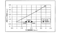
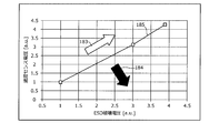
- FIG. 27 is an explanatory diagram showing the measurement results of the relationship between the ESD tolerance of the sense IGBT and the transient sense voltage.
- the gate-emitter capacitance CGE of the sense IGBT 130 increases in the direction from the start point to the end point of the arrow 183. From the results shown in FIG. 27, when the gate-emitter capacitance CGE of the sense IGBT 130 is increased in order to secure the ESD tolerance (withstand against the ESD breakdown voltage described later), the collector-emitter of the sense IGBT 130 is switched during the switching transient period of the sense IGBT 130. It was confirmed that the transient sense voltage applied during the period was high.
- the overcurrent protection function is likely to work due to a malfunction, and the overcurrent protection function causes The operation of the main IGBT 120 may stop.
- a semiconductor substrate has an active region and a termination region.
- the termination region surrounds the periphery of the active region.
- the active region includes a first cell region in which a first insulated gate bipolar transistor is arranged, and a second cell region adjacent to the first cell region.
- the second cell region separates the first region in which the second insulated gate bipolar transistor having an area smaller than that of the first insulated gate bipolar transistor is arranged from the first cell region and the first region.
- a second region is provided on the semiconductor substrate via an oxide film and a first gate electrode layer, and on the first gate electrode layer via an interlayer insulating film. And an emitter electrode of a 2-insulated gate bipolar transistor.
- the termination region has a gate runner on the semiconductor substrate via the oxide film.
- the gate runner surrounds the periphery of the active region.
- the gate runner is electrically connected to the first gate electrode of the first insulated gate bipolar transistor.
- the first gate electrode layer has first and second gate electrode layer portions.
- the first gate electrode layer portion is electrically connected to the second gate electrode of the second insulated gate bipolar transistor.
- the second gate electrode layer portion has a planar shape extending from the first gate electrode layer portion to the gate runner inside the second region, and has a resistance value of 10 ⁇ or more and 5000 ⁇ or less, The first gate electrode layer portion and the gate runner are electrically connected.
- the second gate electrode layer portion has a planar shape that linearly extends from the first gate electrode layer portion to the gate runner, One gate electrode layer portion and the gate runner are connected to each other.
- the second gate electrode layer portion has a planar shape that meanders from the first gate electrode layer portion and reaches the gate runner, The first gate electrode layer portion and the gate runner are connected to each other.
- the second gate electrode layer portion extends in an L shape from the first gate electrode layer portion to the gate runner along an outer periphery of the second region. It has an existing planar shape, and connects the first gate electrode layer portion and the gate runner.
- the semiconductor device according to the present invention is characterized in that, in the above-mentioned invention, the two second gate electrode layer portions are connected in parallel between the first gate electrode layer portion and the gate runner.
- the gate runner has an extending portion that extends along the outer periphery of the second region and surrounds the periphery of the first region.
- the second gate electrode layer section has a planar shape extending from the first gate electrode layer section to the extension section of the gate runner, and the first gate electrode layer section and the extension section of the gate runner. Are connected.
- the third region is a part of the active region excluding the first cell region and the second cell region, and is adjacent to the termination region. It is arranged.
- a second gate electrode layer is provided on the semiconductor substrate in the third region with the oxide film interposed therebetween.
- a gate pad is provided on the second gate electrode layer via the interlayer insulating film.
- the second gate electrode layer has third and fourth gate electrode layer portions.
- the third gate electrode layer portion faces the gate pad with the interlayer insulating film interposed therebetween.
- the fourth gate electrode layer portion has a planar shape that extends from the third gate electrode layer portion to the gate runner inside the third region, and includes the third gate electrode layer portion and the gate runner. It is characterized by being electrically connected.
- the semiconductor device according to the present invention is characterized in that, in the above-mentioned invention, the first insulated gate bipolar transistor has a trench gate structure having the first gate electrode extending in a depth direction of the semiconductor substrate. To do.
- the voltage input to the gate of the second insulated gate bipolar transistor is divided by the second gate electrode layer portion and becomes small.
- the pulse of the ESD waveform is unlikely to have a voltage value that exceeds the gate withstand voltage of the second insulated gate bipolar transistor, and the gate insulating film of the sense IGBT is less likely to cause dielectric breakdown.
- the second gate electrode layer portion does not serve as the gate-emitter capacitance of the second insulated gate bipolar transistor, the transient sense voltage can be suppressed to a level as low as the conventional structure.
- the semiconductor device of the present invention it is possible to improve the trade-off relationship between the improvement of the ESD tolerance of the current sense unit and the reduction of the transient sense voltage.
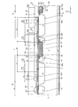
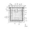
- FIG. 1 is a plan view showing a layout of the semiconductor device according to the first embodiment as viewed from the front surface side of a semiconductor substrate.
- FIG. 2 is an enlarged plan view showing the second cell region of FIG.
- FIG. 3 is an enlarged plan view showing the second cell region of FIG.
- FIG. 4 is an enlarged plan view showing the second cell region of FIG.
- FIG. 5 is an enlarged plan view showing the second cell region of FIG.
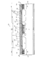
- FIG. 6 is a sectional view showing a sectional structure taken along the section line A-A′ in FIG. 2.
- FIG. 7 is a sectional view showing a sectional structure taken along the section line B-B′ of FIG. 2.
- FIG. 8 is a plan view showing an example of a layout of a part of the semiconductor device according to the second embodiment viewed from the front surface side of the semiconductor substrate.
- FIG. 9 is a plan view showing an example of a layout of a part of the semiconductor device according to the second embodiment viewed from the front surface side of the semiconductor substrate.
- FIG. 10A is a plan view showing an example of a layout of a part of the semiconductor device according to the second embodiment viewed from the front surface side of the semiconductor substrate.
- FIG. 10B is a plan view showing an example of a layout of a part of the semiconductor device according to the second embodiment viewed from the front surface side of the semiconductor substrate.
- FIG. 11 is a plan view showing an example of a layout of a part of the semiconductor device according to the second embodiment viewed from the front surface side of the semiconductor substrate.
- FIG. 12A is a plan view showing an example of a layout of a part of the semiconductor device according to the second embodiment viewed from the front surface side of the semiconductor substrate.
- FIG. 12B is a plan view showing an example of a layout of a part of the semiconductor device according to the second embodiment as viewed from the front surface side of the semiconductor substrate.
- FIG. 13 is a plan view showing an example of a layout of a part of the semiconductor device according to the third embodiment viewed from the front surface side of the semiconductor substrate.
- FIG. 12A is a plan view showing an example of a layout of a part of the semiconductor device according to the second embodiment viewed from the front surface side of the semiconductor substrate.
- FIG. 12B is a plan view showing an example of a layout of a part of the semiconductor device according to the second embodiment as viewed from the front surface side of the semiconductor
- FIG. 14 is a plan view showing an example of a layout of a part of the semiconductor device according to the third embodiment viewed from the front surface side of the semiconductor substrate.
- FIG. 15 is a plan view showing an example of a layout of a part of the semiconductor device according to the third embodiment viewed from the front surface side of the semiconductor substrate.
- FIG. 16 is a plan view showing a layout of a part of the semiconductor device according to the fourth embodiment as viewed from the front surface side of the semiconductor substrate.
- FIG. 17 is a plan view showing a layout of a part of the semiconductor device according to the fourth embodiment as viewed from the front surface side of the semiconductor substrate.
- FIG. 18 is a circuit diagram showing a circuit configuration of a machine model of an ESD evaluation device for evaluating the ESD tolerance of a sense IGBT.
- FIG. 19 is a circuit diagram showing a circuit configuration of a machine model of an ESD evaluation device for evaluating the ESD tolerance of a sense IGBT.
- FIG. 20 is a characteristic diagram showing the relationship between the resistance value of the sense resistor and the ESD tolerance of the sense IGBT of the first embodiment.
- FIG. 21 is a characteristic diagram showing the relationship between the resistance value of the sense resistor and the ESD tolerance of the sense IGBT of the first embodiment.
- FIG. 22 is an explanatory diagram showing the result of simulating the ESD waveform of the sense IGBT of the second embodiment.
- FIG. 23 is an explanatory diagram showing the result of simulating the relationship between the ESD tolerance of the sense IGBT of Example 3 and the transient sense voltage.
- FIG. 24 is an equivalent circuit diagram showing a switching circuit.
- FIG. 25 is an explanatory diagram showing the result of simulating the current/voltage waveform of the conventional semiconductor device.
- FIG. 26 is an explanatory diagram showing the result of simulating the voltage waveform of the sense voltage applied to the sense resistor of FIG.
- FIG. 27 is an explanatory diagram showing the measurement results of the relationship between the ESD tolerance of the sense IGBT and the transient sense voltage.
- FIG. 28 is a plan view showing a layout of a conventional semiconductor device viewed from the front surface side of a semiconductor substrate.
- FIG. 29 is an enlarged plan view showing the vicinity of the current sensing portion of FIG. 28.
- FIG. 30 is an enlarged plan view showing the vicinity of the current sensing portion of FIG. 28.
- FIG. 31 is a sectional view showing a sectional structure taken along the section line AA-AA′ of FIGS.
- FIG. 1 is a plan view showing a layout of the semiconductor device according to the first embodiment as viewed from the front surface side of a semiconductor substrate.
- 2 to 5 are plan views showing the second cell region 3 of FIG. 1 in an enlarged manner. 1 to 5, the contact hole 45 between the gate runner metal 53 and the gate runner 15 and the contact hole 46 between the extending portion 54 of the gate runner metal 53 and the extending portion 16 of the gate runner 15 are shown by thick lines. .. 1 to 4, the gate runner metal 53 and the extending portion 54 of the gate runner metal 53 are not shown.
- FIGS. 1 and 2 are the same portions of FIG. 1, but have different hatching portions.
- the first and second p + type isolation regions 41 and 42 are hatched.
- 3 and 4 the sense polysilicon layer 13 made of polysilicon (poly-Si) and the gate runner 15 are hatched.
- the emitter electrodes 51 and 52, the gate runner metal (metal layer) 53, and the extending portion 54 of the gate runner metal 53 are shown by hatching.
- 6 and 7 are cross-sectional views showing cross-sectional structures taken along the cutting line AA′ and the cutting line BB′ of FIG. 2, respectively.
- the semiconductor device 10 according to the first exemplary embodiment shown in FIGS. 1 to 5 includes a main IGBT (first IGBT) 20 on a semiconductor substrate (semiconductor chip) 7 and a current sense unit for detecting a current flowing through the main IGBT 20.
- Prepare The current sense unit includes a sense IGBT (second IGBT) 30 including a smaller number of unit cells (functional units of elements) having the same configuration as the main IGBT 20 than the main IGBT 20.
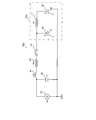
- the equivalent circuit of the semiconductor device 10 according to the first embodiment corresponds to a portion surrounded by a rectangular frame denoted by reference numeral 91b in FIG.
- the main IGBT 20 and the sense IGBT 30 are trench gate type IGBTs having the same structure.
- main IGBT 20 and the sense IGBT 30 have unit cells of the same configuration, but they may have different structures. It suffices to be able to set the ratio of the collector-emitter current when the main IGBT 20 and the sense IGBT 30 are on. Further, it is desirable that the main IGBT 20 and the sense IGBT 30 have the same on-voltage.
- the semiconductor substrate 7 is provided with the active region 1 and the edge termination region 6.
- the active region 1 has first and second cell regions 2 and 3 and has a substantially rectangular planar shape.
- the edge termination region 6 surrounds the periphery of the active region 1.
- the edge termination region 6 is a region between the active region 1 and the end of the semiconductor substrate 7, and relaxes the electric field on the front surface side of the semiconductor substrate 7 to maintain the breakdown voltage.
- the breakdown voltage is the upper limit voltage at which the element does not malfunction or break down at the working voltage.
- a pressure resistant structure such as a field limiting ring (FLR: Field Limiting Ring) 61 and a field plate 63 (see FIG. 7) is arranged.
- FLR Field Limiting Ring
- a first p + type isolation region 41 described later is arranged so as to surround the periphery of the first cell region 2.
- the unit cell of the main IGBT 20 is arranged in a region surrounded by the first p + type isolation region 41 in the first cell region 2.
- the first cell region 2 is an operation region of the main IGBT 20.
- the first cell region 2 is a portion of the active region 1 excluding the second cell region 3, and occupies most of the surface area of the active region 1.
- the first cell region 2 has a substantially rectangular planar shape having a recessed part inwardly.
- the emitter electrode 51 of the main IGBT 20 is provided on the front surface of the semiconductor substrate 7.
- the emitter electrode 51 covers almost the entire first cell region 2.
- the emitter pad 11 is composed of a part of the emitter electrode 51.
- a gate pad metal 55 (see FIG. 17) is arranged on the front surface of the semiconductor substrate 7 near the boundary between the first cell region 2 and the edge termination region 6 with an interlayer insulating film 44 interposed therebetween.
- the gate pad 12 is composed of a part of the gate pad metal 55.
- An input terminal for inputting a gate voltage to the gate electrodes 28 and 38 is electrically connected to the gate pad 12.
- the periphery of the gate pad metal 55 is surrounded by portions (hereinafter referred to as extending portions) 16' and 54' extending from the gate runner 15 and the gate runner metal 53, respectively (see FIGS. 16 and 17).
- the extended portion 54 ′ of the gate runner metal 53 contacts the extended portion 16 ′ of the gate runner 15 via the contact hole 46 ′ of the interlayer insulating film 44.
- the first p + -type isolation region 41 extends over the entire surface region of the semiconductor substrate 7 in the region surrounded by the extension 16 ′ of the gate runner 15.
- the gate pad metal 55 is electrically connected to the gate runner 15 made of polysilicon.
- the unit cell of the sense IGBT 30 is arranged in the second cell region 3.
- the second cell region 3 has a substantially rectangular planar shape adjacent to the edge termination region 6. Specifically, the second cell region 3 is arranged in the recess of the first cell region 2, three sides thereof face the first cell region 2, and the remaining one side faces the edge termination region 6.
- the second cell region 3 has a detection region (first region) 4 in which the unit cells of the sense IGBT 30 are arranged, and a drawing region (second region) 5 for drawing a hole current.
- the main current (collector-emitter current) flowing in the sense IGBT 30 is extracted from the detection region 4 and detected.
- the main current flowing through the main IGBT 20 is calculated based on the amount of the main current flowing through the sense IGBT 30 and the number of unit cells of the sense IGBT 30, and it is determined whether the main current flowing through the main IGBT 20 is an overcurrent.
- the main IGBT 20 is not arranged in the second cell region 3.
- the detection area 4 has, for example, a substantially rectangular planar shape.
- the extraction region 5 surrounds the detection region 4 in a substantially rectangular shape, for example. In the extraction region 5, in the surface region of the semiconductor substrate 7, the first p + type isolation regions 41 and 42 are arranged apart from each other.
- the first p + type separation region 41 occupies most of the surface area of the extraction region 5, and surrounds the detection region 4 in a substantially rectangular shape, for example. Further, the first p + type isolation region 41 extends from the extraction region 5 to the first cell region 2.
- the second p + type separation region 42 is arranged between the first p + type separation region 41 and the detection region 4 and surrounds the periphery of the detection region 4.
- the first and second p + type isolation regions 41 and 42 are electrically connected to the emitter electrode 51 of the main IGBT 20 and the emitter electrode 52 of the sense IGBT 30, respectively.
- the first cell region 2 is separated from the regions other than the first cell region 2 by the pn junction between the first p + type isolation region 41 and the n ⁇ type drift region 21 (see FIGS. 5 and 6).
- the pn junction between the second p + type isolation region 42 and the n ⁇ type drift region 21 separates the detection region 4 in the second cell region 3 from the regions other than the detection region 4.
- the first and second p + type isolation regions 41 and 42 are generated in the edge termination region 6 when the avalanche is generated in the edge termination region 6 when the main IGBT 20 is turned off, and the first and second cell regions are formed in the semiconductor substrate 7. It has a function of drawing out hole currents flowing toward the sides 2 and 3 to the emitter electrodes 51 and 52, respectively.
- a sense polysilicon layer (first gate electrode layer) 13 made of polysilicon (poly-Si) is arranged on the front surface of the semiconductor substrate 7 with the field oxide film 43b interposed therebetween. ing.
- the sense polysilicon layer 13 covers almost the entire extraction region 5 via the field oxide film 43b.
- the sense polysilicon layer 13 has a built-in resistor portion 17 and a sense capacitance portion 18 made of polysilicon (see FIG. 4).
- the built-in resistor section 17 and the sense capacitance section 18 are arranged apart from each other. In FIG. 4, the ranges of the built-in resistor section 17 and the sense capacitance section 18 are surrounded by thick two-dot chain lines and thick broken lines, respectively.
- the built-in resistor portion 17 is a connecting portion between the gate electrode 38 (see FIGS. 6 and 7) of the sense IGBT 30 and the gate runner 15.
- the built-in resistor portion 17 connects the first portion (first gate electrode layer portion) 17a electrically connected to the gate electrode 38 (see FIG. 7) of the sense IGBT 30 and the first portion 17a to the gate runner 15.
- a second portion (second gate electrode layer portion) 17b see FIGS. 3 and 4).
- the series resistance of the first and second portions 17a and 17b of the built-in resistance portion 17 functions as a built-in resistance of the sense IGBT 30, and the resistance value is the sum of the resistance values of the first and second portions 17a and 17b of the built-in resistance portion 17. ..
- a built-in resistor section 17 that functions as a built-in resistor of the sense IGBT 30 is electrically connected between the gate electrode 28 of the main IGBT 20 and the gate electrode 38 of the sense IGBT 30.
- the first portion 17 a of the built-in resistor portion 17 surrounds the periphery of the detection area 4.
- the contour shape of the outer peripheral end of the first portion 17 a of the built-in resistor portion 17 is a substantially rectangular shape larger than the detection area 4.
- the outer peripheral end portion 13b of the first portion 17a of the built-in resistor portion 17 is preferably separated from the detection region 4 in the second direction Y described later. Since the outer peripheral end portion 13b of the first portion 17a of the built-in resistor portion 17 is separated from the detection region 4, the imbalance of the built-in resistance value caused by the trench 36 of the sense IGBT 30 can be reduced.
- An inner peripheral end portion (end portion on the detection region 4 side) 13a of the first portion 17a of the built-in resistor portion 17 extends from the extraction region 5 to the detection region 4 and contacts the gate electrode 38 of the sense IGBT 30 (see FIG. 7). ).
- the second portion 17b of the built-in resistor portion 17 is located between the first portion 17a of the built-in resistor portion 17 and the gate runner 15, and connects the first portion 17a of the built-in resistor portion 17 and the gate runner 15.
- the second portion 17b of the built-in resistor portion 17 is arranged in line symmetry with respect to an axis (axis parallel to the cutting line BB') that is perpendicular to the gate runner 15 at the connecting portion with the gate runner 15. For example, it extends linearly in the extraction region 5 in a direction (hereinafter, referred to as a first direction) X parallel to the axis and parallel to the front surface of the semiconductor substrate 7.
- the resistance value of the second portion 17b of the built-in resistor portion 17 is calculated by ⁇ w1/(w2 ⁇ t).
- ⁇ is the resistivity of the sense polysilicon layer 13
- w1 is the length of the second portion 17b of the built-in resistance portion 17 in the first direction X
- (w2 ⁇ t) is the length of the built-in resistance portion 17.
- the sense capacitance section 18 is arranged apart from the built-in resistance section 17 by a predetermined distance w3, and surrounds the circumference of the built-in resistance section 17. 2 to 4, the outer peripheral end portion of the first portion 17a of the built-in resistor portion 17 is shown by a thick two-dot chain line with reference numeral 13b. The inner circumference of the sense capacitor section 18 is indicated by a thick broken line with a reference numeral 13c.
- the sense capacitor section 18 is connected to the extending section 16 of the gate runner 15 described later.
- the capacitance formed by the sense capacitance section 18, the interlayer insulating film 44, and the emitter electrode 52 becomes a part of the gate-emitter capacitance CGE of the sense IGBT 30.
- An emitter electrode 52 of the sense IGBT 30 extends on the sense polysilicon layer 13 via an interlayer insulating film 44 (see FIG. 6). Further, when it is desired to reduce the capacity of the sense IGBT 30, the sense capacitor section 18 may not be provided.
- the emitter electrode 52 of the sense IGBT 30 is provided over almost the entire second cell region 3.
- the emitter electrode 52 of the sense IGBT 30 is arranged apart from the emitter electrode 51 of the main IGBT 20.
- the sense emitter pad 14 is a portion of the emitter electrode 52 exposed in the opening 48b of the passivation film 47, and is formed of a part of the emitter electrode 52.
- the built-in resistor portion 17 is arranged between the sense emitter pad 14 and the gate runner 15.
- the sense emitter pad 14 faces the sense capacitor section 18 with the interlayer insulating film 44 interposed therebetween.
- the gate runner 15 is arranged in the edge termination area 6 and surrounds the periphery of the active area 1.
- the gate runner 15 has a portion (hereinafter referred to as an extension portion) 16 that extends to the second cell region 3 along the outer periphery of the second cell region 3.
- the extension portion 16 of the gate runner 15 is a part of the sense polysilicon layer 13.
- the extending portion 16 of the gate runner 15 surrounds the periphery of the second cell region 3.
- One polysilicon layer formed by the gate runner 15 and the extension portion 16 of the gate runner 15 extends along the outer periphery of the first cell region 2 and surrounds the periphery of the first cell region 2.
- the gate runner metal 53 and the extending portion 54 of the gate runner metal 53 respectively face the gate runner 15 and the extending portion 16 of the gate runner 15 in the thickness direction Z with the interlayer insulating film 44 interposed therebetween.
- Z is in contact with the gate runner 15 and the extension 16 of the gate runner 15 through contact holes 45 and 46 penetrating the interlayer insulating film 44.
- the inner circumference of the sense polysilicon layer 13 (the end portion on the detection region 4 side) is shown by a broken line with a reference numeral 13a.
- the inner circumference (the end portion on the active region 1 side) and the outer circumference (the end portion on the end portion side of the semiconductor substrate 7) of the portion surrounding the periphery of the active region 1 of the gate runner 15 are respectively denoted by reference numerals. It is indicated by a broken line with 15a and 15b.
- Reference numeral 16a is attached to the end of the extending portion 16 of the gate runner 15 on the active region 1 side.
- Gate electrodes 28 and 38 (see FIGS. 6 and 7) of the main IGBT 20 and the sense IGBT 30 are electrically connected to the gate runner 15.
- the semiconductor device 10 according to the first embodiment includes a plurality of unit cells of the main IGBT 20 and a plurality of unit cells of the sense IGBT 30, respectively in the first and second cell regions of the active region 1.
- the unit cell of the main IGBT 20 includes a p-type base region 22, an n + -type emitter region 24, a p + -type contact region 25, a trench 26, a gate insulating film 27 and a gate electrode provided on the front surface side of the semiconductor substrate 7. 28.
- the unit cell of the main IGBT 20 has a general trench gate structure having a gate electrode 28 embedded in the trench 26 via a gate insulating film 27 and extending in the depth direction (thickness direction Z) of the semiconductor substrate 7. ..
- the unit cell of the main IGBT 20 is arranged in a region surrounded by the first p + type isolation region 41 in the first cell region 2.
- the p type base region 22, the n + type emitter region 24 and the p + type contact region 25 are provided in the surface region of the front surface of the semiconductor substrate 7.
- the n + type emitter region 24 and the p + type contact region 25 are provided between the adjacent trenches 26 (mesa region) at a position shallower than the p type base region 22 from the front surface of the semiconductor substrate 7.
- the n + type emitter region 24 is not arranged and only the p + type contact region 25 is arranged.
- an n ⁇ type drift region 21 is provided at a position deeper than the p type base region 22 from the front surface of the semiconductor substrate 7.
- a region (hereinafter, referred to as an accumulation region) 23 in which electric charges (holes) that become minority carriers at the time of turning on are accumulated may be provided.
- the accumulation region 23 is an n-type region having a higher impurity concentration than the n ⁇ -type drift region 21.
- the trenches 26 are arranged, for example, in a stripe shape extending in the first direction X described above.
- the gate electrode 28 is provided inside the trench 26 via a gate insulating film 27.
- One unit cell of the main IGBT 20 is configured by the one trench 26 in which the gate electrode 28 is buried and the mesa region adjacent to the trench 26.
- the first p + type isolation region 41 contacts the p type base region 22 and the p + type contact region 25 in the vicinity of the outer periphery of the first cell region 2.
- the depth of the first p + type isolation region 41 is deeper than the depth of the trench 26.
- the emitter electrode 51 of the main IGBT 20 is in contact with the n + type emitter region 24, the p + type contact region 25, and the first p + type isolation region 41 via a contact hole penetrating the interlayer insulating film 44 in the thickness direction Z.
- the emitter electrode 51 may be electrically connected to the n + type emitter region 24, the p + type contact region 25, and the first p + type isolation region 41 via a barrier metal and a contact plug.
- the barrier metal is made of a metal that has high adhesiveness with the semiconductor portion (semiconductor substrate 7) and is in ohmic contact with the semiconductor portion.
- the barrier metal may be, for example, a laminated film formed by sequentially laminating a titanium (Ti) film and a titanium nitride (TiN) film.
- the contact plug is, for example, a metal film made of tungsten (W), which has a high embedding property, and is embedded in the contact hole of the interlayer insulating film 44 via a barrier metal.
- the emitter electrode 51 is, for example, an aluminum silicon (Al—Si) electrode.
- the emitter electrode 51 is electrically insulated from the gate electrode 28 by the interlayer insulating film 44.
- the emitter electrode 51 is covered with a passivation film 47.
- the portion of the emitter electrode 51 exposed in the opening 48a of the passivation film 47 constitutes the emitter pad 11.
- the p + -type collector region 29 of the main IGBT 20 is provided over the entire back surface of the semiconductor substrate 7.
- the collector electrode 56 of the main IGBT 20 is provided over the entire back surface of the semiconductor substrate 7.
- the unit cell of the sense IGBT 30 is arranged in the region surrounded by the second p + type isolation region 42 in the detection region 4 of the second cell region 3.
- the unit cell of the sense IGBT 30 includes a p-type base region 32, an n + -type emitter region 34, a p + -type contact region 35, a trench 36, a gate insulating film 37 and a gate electrode provided on the front surface side of the semiconductor substrate 7. It is composed of 38.
- the unit cell of the sense IGBT 30 has a general trench gate structure having a gate electrode 38 embedded in the trench 36 and extending in the depth direction of the semiconductor substrate 7.
- n + -type emitter region 34 and the p + -type contact region 35 are provided between the adjacent trenches 36 (mesa region) at a position shallower than the p-type base region 32 from the front surface of the semiconductor substrate 7.
- the n + type emitter region 34 is not arranged, but only the p + type contact region 35 is arranged.
- An n ⁇ type drift region 21 extends from the first cell region 2 at a position deeper than the p type base region 32 from the front surface of the semiconductor substrate 7.
- a storage region may be provided between the p-type base region 32 and the n ⁇ -type drift region 21.
- the reason why the sense IGBT 30 need not be provided with the storage region is as follows. By not providing the storage region of the sense IGBT 30, it is possible to reduce the IE (Injection Enhanced: electron injection promotion) effect in the sense IGBT 30, and it is possible to suppress a decrease in turn-off resistance due to the accumulation of minority carriers.
- IE injection Enhanced: electron injection promotion
- the trenches 36 are arranged, for example, in a stripe shape that extends in the same first direction X as the direction in which the trenches 26 of the main IGBT 20 extend.
- the gate electrode 38 is provided inside the trench 36 via the gate insulating film 37.
- One trench 36 in which the gate electrode 38 is embedded and the mesa region adjacent to the trench 36 constitute one unit cell of the sense IGBT 30.
- the p-type base region 32, the n + -type emitter region 34, the p + -type contact region 35, and the trench 36 have the same depth as the corresponding parts of the main IGBT 20.
- the second p + type isolation region 42 contacts the p type base region 32 and the p + type contact region 35 in the vicinity of the outer periphery of the second cell region 3.
- the depth of the second p + type isolation region 42 is the same as the depth of the first p + type isolation region 41.
- the p-type base region 32 and the p + -type contact region 35 may extend from the detection region 4 toward the extraction region 5 in the first direction X inside the second p + -type isolation region 42.
- the second p + type isolation region 42 may extend from the extraction region 5 to reach the trench 36 arranged closest to the extraction region 5 side, or may include the trench 36.
- the emitter electrode 52 of the sense IGBT 30 is in contact with the n + type emitter region 34, the p + type contact region 35, and the second p + type isolation region 42 via a contact hole penetrating the interlayer insulating film 44 in the thickness direction Z.
- the emitter electrode 52 may be electrically connected to the n + type emitter region 34, the p + type contact region 35, and the second p + type isolation region 42 via a barrier metal and a contact plug.
- the materials of the emitter electrode 52, the barrier metal and the contact plug are the same as the materials of the emitter electrode 51, the barrier metal and the contact plug of the main IGBT 20.
- the emitter electrode 52 is electrically insulated from the gate electrode 38 by the interlayer insulating film 44.
- the emitter electrode 52 is covered with the passivation film 47.
- the portion of the emitter electrode 52 exposed in the opening 48b of the passivation film 47 constitutes the sense emitter pad 14.
- the sense emitter pad 14 may be arranged in the extraction region 5 of the second cell region 3, for example.
- P + -type collector region 29 and collector electrode 56 of the main IGBT20 also serves as the p + -type collector region and the collector electrode of the sense IGBT30 respectively.
- first and second p + -type isolation regions 41 and 42 are selectively provided in the surface region of the front surface of the semiconductor substrate 7.
- the first and second p + type isolation regions 41 and 42 are separated by a local insulating film 43a such as a field oxide film or LOCOS (Local Oxidation of Silicon) provided on the front surface of the semiconductor substrate 7.
- the first p + type isolation region 41 extends from the extraction region 5 to the outer peripheral portion of the first cell region 2.
- the second p + type separation region 42 is disposed closer to the detection region 4 side than the first p + type separation region 41, and extends from the extraction region 5 to the outer peripheral portion of the detection region 4.
- the built-in resistance portion 17 and the sense capacitance portion 18 of the sense polysilicon layer 13 are provided on the front surface of the semiconductor substrate 7 with the field oxide film 43b interposed therebetween.
- the first portion 17a of the built-in resistor portion 17 faces the first and second p + -type isolation regions 41 and 42 in the thickness direction Z with the field oxide film 43b and the local insulating film 43a interposed therebetween.
- the first portion 17a of the built-in resistor portion 17 extends into the trench 36 of the sense IGBT 30, for example, at an end portion in the first direction X, and contacts the gate electrode 38.
- the second portion 17b of the built-in resistor portion 17 is arranged closer to the edge termination region 6 side than the first portion 17a of the built-in resistor portion 17, and is connected to the first portion 17a of the built-in resistor portion 17.
- the second portion 17b of the built-in resistor portion 17 faces the first p + -type isolation region 41 with the field oxide film 43b interposed therebetween in the thickness direction Z.
- the sense capacitance section 18 is arranged closer to the first cell region 2 side than the built-in resistance section 17 and apart from the built-in resistance section 17.
- the sense capacitor section 18 faces the first p + type isolation region 41 with the field oxide film 43b interposed therebetween in the thickness direction Z.
- the second portion 17b of the built-in resistor portion 17 extends to the edge termination region 6 side and is connected to the gate runner 15.
- the sense capacitance portion 18 also serves as the extending portion 16 of the gate runner 15 and is connected to the gate runner 15.
- the emitter electrode 52 of the sense IGBT 30 extends from the detection region 4 with the interlayer insulating film 44 interposed therebetween.
- the emitter electrode 51 of the main IGBT 20 extends from the first cell region 2 with the interlayer insulating film 44 interposed therebetween.
- the first and second portions 17a and 17b of the built-in resistor portion 17 and the sense capacitance portion 18 are electrically insulated from the emitter electrodes 51 and 52 by the interlayer insulating film 44.
- the gate runner metal 53 and the extending portion 54 of the gate runner metal 53 are in contact with the gate runner 15 and the extending portion 16 of the gate runner 15 through the contact holes 45 and 46 of the interlayer insulating film 44, respectively.
- FIGS. 6 and 7 show a case where two contact holes 45 and 46 are provided, respectively, the number of contact holes 45 and 46 can be variously changed.
- one or more field limiting rings 61 are provided in a concentric pattern surrounding the active region 1 in the surface region of the front surface of the semiconductor substrate 7.
- a polysilicon layer 62 is provided on each field limiting ring 61 via a field oxide film 43b.
- a field plate 63 is provided on the polysilicon layer 62 with an interlayer insulating film 44 interposed therebetween. The field plate 63 is in contact with the polysilicon layer 62 through the contact hole of the interlayer insulating film 44.
- ESD electrostatic discharge
- the ESD machine model is an RLC circuit (resistor (R), inductance (Lm) and capacitor (C)) connected to the gate pad 112 of the IGBT as shown in FIG. Therefore, the ESD waveform satisfies the resonance condition of the RLC circuit and oscillates (see FIG. 22).
- the gate insulating film 137 in the gate trench 136 of the sense IGBT 130 is broken down. Therefore, the ESD tolerance of the sense IGBT 130 needs to be set so that the voltage value of the first pulse of the ESD waveform is equal to or lower than the gate withstand voltage of the sense IGBT 130.
- the gate of the sense IGBT is connected to the high-resistance built-in resistor formed of the second portion of the built-in resistance portion made of polysilicon.
- This built-in resistor portion lowers the dV/dt of the first pulse voltage of the ESD, so that the peak voltage of the first pulse of the ESD waveform decreases.
- the peak voltage of the first pulse of the ESD waveform is less likely to exceed the gate withstand voltage of the sense IGBT, and the gate insulating film in the gate trench of the sense IGBT is less likely to cause dielectric breakdown.
- the gate-emitter capacitance CGE of the sense IGBT does not increase because the built-in resistor portion made of polysilicon is provided. Therefore, even if the ESD resistance is improved by the built-in resistor portion, the transient sense voltage, which increases in proportion to the size of the gate-emitter capacitance CGE of the sense IGBT, is made to be about the same as the conventional structure without the built-in resistor. You can As a result, only the ESD withstand capability can be improved while maintaining the transient sense voltage low, so that the trade-off relationship between the improvement of the ESD withstand capability of the current sense unit and the reduction of the transient sense voltage can be improved.
- FIGS. 8 to 12 are plan views showing an example of a layout of a part of the semiconductor device according to the second embodiment viewed from the front surface side of the semiconductor substrate.
- the layout of the entire semiconductor device 10' according to the second embodiment viewed from the front surface side of the semiconductor substrate 7 is the same as that of the semiconductor device 10 according to the first embodiment (see FIG. 1).
- the second cell region 3 of FIG. 1 is enlarged and the sense polysilicon layer 13 and the gate runner 15 are shown by hatching.
- the range of the second portion 17b of the built-in resistor portion 17 is surrounded by a thick two-dot chain line.
- the emitter electrodes 51 and 52 are not shown.
- the semiconductor device 10 ′ according to the second embodiment differs from the semiconductor device 10 according to the first embodiment in that the area occupied by the first portion 17 a ′ of the built-in resistor portion 17 in the extraction region 5 is small.
- the first portion 17a' of the built-in resistor portion 17 may be arranged so that the second portion 17b of the built-in resistor portion 17 and the gate electrode 38 of the sense IGBT 30 can be connected to each other.
- the first portion 17 a ′ of the built-in resistor portion 17 is provided along the boundary between the detection region 4 and the extraction region 5 and surrounds the detection region 4 in a substantially rectangular shape.
- the contour shape of the outer peripheral end portion of the first portion 17 a ′ of the built-in resistor portion 17 is a substantially rectangular shape slightly larger than the detection area 4.
- the second portion 17b of the built-in resistor portion 17 has a linear planar shape extending in the first direction X, as in the first embodiment.
- the second portion 17b of the built-in resistor portion 17 is located between the first portion 17a′ of the built-in resistor portion 17 and the gate runner 15 as in the first embodiment, and the first portion 17a of the built-in resistor portion 17 is formed. 'And the gate runner 15 are connected (FIG. 8).
- the first portion 17a' of the built-in resistor portion 17 and the extending portion 16 of the gate runner 15 may be connected by the second portion 17b' of the built-in resistor portion 17 (Fig. 9).
- the second portion 17b' of the built-in resistor portion 17 is located between the first portion 17a' of the built-in resistor portion 17 and the extending portion 16 of the gate runner 15.
- the sense emitter pad 14 is arranged in the emitter electrode 52 between the regions surrounded by the extension 16 of the gate runner 15.
- the second portion 19 of the built-in resistor portion 17 may have a planar shape that extends meandering in the X direction or the Y direction from the first portion 17a′ of the built-in resistor portion 17 and reaches the gate runner 15. (FIGS. 10B, 10A).
- the second portion 19 of the built-in resistor portion 17 is preferably connected to the first portion 17 a ′ of the built-in resistor portion 17 at a position facing the center of the detection region 4.
- the sense capacitor section 18 ′ may increase the occupied area in the extraction region 5 by an amount corresponding to the reduced occupied area of the first portion 17 a ′ of the built-in resistor section 17 (FIGS. 8, 9, 10A, 10B).
- a configuration may be adopted in which only the extending portion 16 of the gate runner 15 is configured without providing the sense capacitance portion 18' in the extraction region 5 (FIGS. 11, 12A, 12B).
- the interlayer insulating film and the field oxide film are sandwiched in the depth direction.
- the sense polysilicon layer 13 does not exist between the opposing sense emitter pad 14 and the semiconductor substrate 7 (FIGS. 11, 12A, 12B).
- the sense capacitor portion 18 ′ is not provided in the extraction region 5 and only the extending portion 16 of the gate runner 15 is configured, one end of the second portion 19 ′ of the built-in resistor portion 17 is connected to the gate runner 15,
- the built-in resistor portion 17 may extend substantially around the first portion 17a′ so as to surround the first portion 17a′, and the other end thereof may be connected to the first portion 17a′ (FIG. 12B).
- the other end of the second portion 19 ′ of the built-in resistor portion 17 is connected to the first portion 17 a ′ of the built-in resistor portion 17 at a position facing the center of the detection region 4.
- the semiconductor device 10′ according to the second exemplary embodiment shown in FIGS. 10A and 10B is applied to the semiconductor device 10′ according to the second exemplary embodiment shown in FIG. However, it may have a planar shape which meanders from the first portion 17 a ′ of the built-in resistor portion 17 and extends to the extended portion 16 of the gate runner 15.
- the semiconductor device 10′ according to the second embodiment shown in FIG. 11 is applied to the semiconductor device 10′ according to the second embodiment shown in FIG. 9, and the extension portion of the gate runner 15 is provided without providing the sense capacitance portion 18′. Only 16 may be configured.
- the semiconductor device 10' according to the second embodiment shown in FIGS. 10A, 10B and 11 By applying the semiconductor device 10' according to the second embodiment shown in FIGS. 10A, 10B and 11 to the semiconductor device 10' according to the second embodiment shown in FIG. Only the extending portion 16 of the gate runner 15 is formed in a planar shape that extends in a meandering manner from the first portion 17a′ of the resistor portion 17 to the extending portion 16 of the gate runner 15 and does not include the sense capacitance portion 18′. It may be configured. In the semiconductor device 10 according to the first embodiment, the sense capacitor section 18 may not be provided, and the extending portion 16 of the gate runner 15 of the semiconductor device 10' according to the second embodiment shown in FIG. 11 may be arranged.
- the built-in resistance part detects the sense IGBT. Functions as a built-in resistor of. Therefore, even if the planar shapes of the first and second portions of the built-in resistance portion and the sense capacitance portion are variously changed, the same effect as that of the first embodiment can be obtained.
- FIGS. 3 are plan views showing an example of a layout of a part of the semiconductor device according to the third embodiment viewed from the front surface side of the semiconductor substrate.
- the layout of the entire semiconductor device 70 according to the third embodiment viewed from the front surface side of the semiconductor substrate 7 is the same as that of the semiconductor device 10 according to the first embodiment (see FIG. 1).
- 13 to 15 the second cell region 3 of FIG. 1 is enlarged and the sense polysilicon layer 13 and the gate runner 15 are shown by hatching.
- FIGS. 1 are plan views showing an example of a layout of a part of the semiconductor device according to the third embodiment viewed from the front surface side of the semiconductor substrate.
- the layout of the entire semiconductor device 70 according to the third embodiment viewed from the front surface side of the semiconductor substrate 7 is the same as that of the semiconductor device 10 according to the first embodiment (see FIG. 1).
- 13 to 15 the second cell region 3 of FIG. 1 is enlarged and the sense polysilicon layer 13 and the gate runner 15 are shown by hatching.
- the range of the second portions 71, 73, 74, 73′, 74′ of the built-in resistor portion 17 is surrounded by a thick two-dot chain line. Further, in FIGS. 13 to 15, the emitter electrodes 51 and 52 (see FIGS. 1, 4 and 5) are omitted from the drawing.
- the semiconductor device 70 according to the third embodiment is different from the semiconductor device 10 ′ according to the second embodiment shown in FIG. 8 in that the second portion 71 of the built-in resistor portion 17 is elongated in the extraction region 5 with a narrow width w11. The point is that it is extended to have high resistance.
- the sense capacitance section 72 is connected to the gate runner 15. The sense capacitance portion 72 does not contact the extension portion 16 of the gate runner 15. The sense capacitor portion 72 occupies most of the surface area of the extraction region 5.
- the detection area 4 is arranged farther from the gate runner 15 than the sense capacitance section 72, and is surrounded by the extraction area 5.
- the first portion 17a' of the built-in resistor portion 17 is provided along the boundary between the detection region 4 and the extraction region 5 and surrounds the detection region 4 in a substantially rectangular shape, as in the second embodiment.
- the contour shape of the outer peripheral end of the first portion 17a' of the built-in resistor portion 17 is a substantially rectangular shape slightly larger than the detection region 4 as in the second embodiment.
- the first portion 17a′ of the built-in resistor portion 17 may be provided with the same width w12 over the entire circumference surrounding the circumference of the detection region 4, or may have a width w12′ that differs by a predetermined side among the rectangular sides. It may be provided.
- the second portion 71 of the built-in resistor portion 17 has an L-shaped planar shape.
- the second portion 71 of the built-in resistance portion 17 is located between the gate runner 15 and the sense capacitance portion 72 and the extending portion 16 of the gate runner 15 in the first cell region 2 on the outer periphery of the second cell region 3. It extends along two opposite sides.
- the one end of the L shape of the second portion 71 of the built-in resistor portion 17 is connected to the gate runner 15.
- the other L-shaped end of the second portion 71 of the built-in resistance portion 17 is connected to the first portion 17a' of the built-in resistance portion 17.
- the first portion 17a' of the built-in resistor portion 17 may be surrounded by the sense capacitance portion 72 on three sides.
- the sense emitter pad 14 is arranged between the first portion 17 a ′ of the built-in resistor portion 17 and the gate runner 15.
- the sense emitter pad 14 faces the sense capacitance section 72 with the interlayer insulating film interposed therebetween.
- the semiconductor device 70 according to the third embodiment shown in FIGS. 14 and 15 is different from the semiconductor device 70 according to the third embodiment shown in FIG. 13 in that in the extraction region 5, the L-shaped portion of the built-in resistor portion 17 is formed. This is the point where two second portions each having a planar shape are arranged.
- the combined resistance of the two second portions of the built-in resistance unit 17 functions as the built-in resistance of the sense IGBT 30.
- the two second portions of the built-in resistor portion 17 are arranged, for example, as follows.
- one of the second portions 73 of the built-in resistor portion 17 has an outer periphery of the second cell region 3 between the gate runner 15 and the sense capacitance portion 72 ′ and the extending portion 16 of the gate runner 15. Extending along two sides facing the first cell region 2.
- One L-shaped end of the second portion 73 of the built-in resistor portion 17 is connected to the gate runner 15.
- the other end of the L-shaped second portion 73 of the built-in resistor portion 17 is connected to the gate runner 15 side of the first portion 17a' of the built-in resistor portion 17.
- the other second portion 74 of the built-in resistor portion 17 is arranged at a position facing the one second portion 73 of the built-in resistor portion 17 with the sense capacitance portion 72 ′ interposed therebetween.
- the other second portion 74 of the built-in resistor portion 17 is located between the sense capacitor portion 72 ′ and the extending portion 16 of the gate runner 15 from the gate runner 15 side, and is located on the outer periphery of the second cell region 3 in the first cell region.
- the one second portion 73 extends from one side where the second portion 73 is not disposed to one side that is continuous with the one side.
- the L-shaped end of the other second portion 74 of the built-in resistor portion 17 is connected to the gate runner 15 via the part 75 of the sense polysilicon layer 13.
- the other L-shaped end of the other second portion 74 of the built-in resistor portion 17 is connected to the extension portion 16 side of the gate runner 15 of the first portion 17 a ′ of the built-in resistor portion 17.
- the sense capacitor section 72' has, for example, a substantially rectangular planar shape.
- the L-shaped other ends of the second portions 73 ′ and 74 ′ of the built-in resistor portion 17 both extend between the first portion 17 a ′ of the built-in resistor portion 17 and the sense capacitance portion 72 ′. You may let me.
- the L-shaped ends of the second portions 73 ′ and 74 ′ of the built-in resistor portion 17 are connected to different portions of the gate runner 15.
- the other ends of the L-shapes of the second portions 73' and 74' of the built-in resistor portion 17 are both connected to the first portion 17a' of the built-in resistor portion 17.
- the same effects as those of the first and second embodiments can be obtained. Further, according to the third embodiment, by extending the second portion of the built-in resistance portion with a narrow width for a long time within the extraction region, the built-in resistance of the sense IGBT can be made high.
- 16 and 17 are plan views showing a layout of a part of the semiconductor device according to the fourth embodiment as viewed from the front surface side of the semiconductor substrate.
- the layout of the entire semiconductor device 80 according to the fourth embodiment viewed from the front surface side of the semiconductor substrate 7 is the same as that of the semiconductor device 10 according to the first embodiment (see FIG. 1).
- 16 and 17 are enlarged plan views showing the vicinity of the gate pad 12 of the main IGBT of FIG. 16 and 17 are the same parts in FIG. 1, but the hatched parts are different.
- the emitter electrode 51 and the gate pad metal 55 are not shown.
- the polysilicon layer 83 and the gate runner 15 are hatched.
- the gate runner metal 53, the extended portion 54 ′ of the gate runner metal 53, and the gate pad metal 55 are shown by hatching.
- the range of the second portion 81b of the built-in resistor portion 81 is surrounded by a thick chain double-dashed line.
- the contact hole 46' and the contact 45' between the gate pad metal 55 and the polysilicon layer 83 are shown by thick lines.
- the semiconductor device 80 according to the fourth embodiment is different from the semiconductor device 10 according to the first embodiment in that instead of the second cell region 3, a polysilicon layer is formed in a region (third region) where the gate pad 12 is arranged. This is the point where 83 is arranged.
- the equivalent circuit of the semiconductor device 80 according to the fourth embodiment corresponds to a portion surrounded by a rectangular frame denoted by reference numeral 91a in FIG.
- the polysilicon layer 83 is provided on the front surface of the semiconductor substrate 7 via the field oxide film 43b.
- the polysilicon layer 83 has a built-in resistance portion 81 and an extension portion 16 ′ of the gate runner 15.
- the built-in resistor portion 81 is a connecting portion that electrically connects the gate pad metal 55 and the gate runner 15 which are arranged apart from each other.
- the built-in resistor portion 81 is connected to the gate electrode 28 of the main IGBT 20 via the gate runner 15.
- the built-in resistor portion 81 includes a first portion (third gate electrode layer portion) 81a electrically connected to the gate pad 12 and a second portion (first portion 81a) electrically connecting the first portion 81a to the gate runner 15. 4 gate electrode layer portion) 81b.
- the first portion 81a of the built-in resistor portion 81 faces the entire gate pad 12 with the interlayer insulating film 44 interposed therebetween.
- the gate pad 12 is composed of a portion of the gate pad metal 55 exposed in the opening of the passivation film 47.
- the gate pad metal 55 is provided on the polysilicon layer 83 via the interlayer insulating film 44.
- the first portion 81a of the built-in resistor portion 81 faces the entire surface of the gate pad 12 with the interlayer insulating film 44 interposed therebetween, and the contour shape of the outer peripheral end of the first portion 81a of the built-in resistor portion 81 is at least the gate pad. It may be a substantially rectangular shape slightly larger than 12.
- the second portion 81b of the built-in resistor portion 81 connects the first portion 81a of the built-in resistor portion 81 and the extending portion 16' of the gate runner 15.
- the resistance value of the first portion 81a of the built-in resistor portion 81 is smaller than the resistance value of the second portion 81b, and the resistance value of the built-in resistor portion 81 is smaller than that of the second portion 81b.
- the second portion 81b mainly functions as a built-in resistor of the sense IGBT 30.
- the second portion 81b of the built-in resistor portion 81 is located, for example, between the first portion 81a of the built-in resistor portion 81 and the extending portion 16′ of the gate runner 15, and the first portion 81a of the built-in resistor portion 81 is connected to the gate. It has a linear planar shape extending to the extending portion 16 ′ of the runner 15.
- the second portion 81b of the built-in resistor portion 81 is located, for example, between the first portion 81a of the built-in resistor portion 81 and the gate runner 15, and is located between the first portion 81a of the built-in resistor portion 81 and the gate. You may connect with the runner 15.
- Extending part 16' of gate runner 15 has a substantially U-shaped planar shape, and both ends of the U-shape are connected to different parts of gate runner 15, respectively.
- the gate runner 15 and the extending portion 16 ′ of the gate runner 15 form a substantially rectangular planar shape surrounding the built-in resistor portion 81.
- both the second cell region 3 and the region in which the gate pad 12 is arranged are provided.
- the built-in resistor parts 17 and 81 may be arranged in each.
- the sense resistor is connected to the gate resistance by providing the built-in resistor portion in the region where the gate pad is arranged.
- the main IGBT is also connected to the gate resistor. Becomes As a result, the mirror period of the gate voltage of the main IGBT is increased and the switching loss is deteriorated. Therefore, it is possible to prevent deterioration of switching loss by providing a built-in resistance portion between the gate runner of the sense IGBT and the detection region.
- Example 1 Next, the ESD tolerance of the sense IGBT 30 was verified.
- 18 and 19 are circuit diagrams showing the circuit configuration of the machine model of the ESD evaluation device for evaluating the ESD tolerance of the sense IGBT.
- 20 and 21 are characteristic diagrams showing the relationship between the resistance value of the sense resistor and the ESD tolerance of the sense IGBT of the first embodiment. 20 and 21 are measured using the ESD evaluation circuits 90a and 90b shown in FIGS. 18 and 19, respectively.
- a semiconductor device 91a shown in FIG. 18 corresponds to the semiconductor device 80 (see FIGS. 16 and 17) according to the fourth embodiment, and is provided between the main IGBT 20 and the sense IGBT 30 connected in parallel, and the gate of the main IGBT 20 and the switch 92. And a built-in resistor RG connected to.
- the built-in resistor RG of the semiconductor device 91a corresponds to the second portion 81b of the built-in resistor portion 81.
- the switch 92 of the ESD evaluation circuit 90a shown in FIG. 18 When the switch 92 of the ESD evaluation circuit 90a shown in FIG. 18 is turned on, the charge charged in the capacitor 96 is supplied to the main IGBT 20 and the sense IGBT 30 until the voltage becomes a constant voltage (this constant voltage will be referred to as ESD Applied voltage). Further, the emitter of the sense IGBT 30 is grounded, but the emitter of the main IGBT 20 is not grounded, so that charges are supplied only between the gate and the emitter of the sense IGBT 30.
- the positive electrode of the current source 93 is connected to the switch 92, and the negative electrode is grounded. Between the positive electrode of the current source 93 and the switch 92, a wiring inductance 94 that assumes the inductance Lm of the wiring of the device and a resistive load 95 that assumes the resistance Rm of the wiring are connected in series. Between the positive electrode of the current source 93 and the wiring inductance 94, a capacitor 96 is connected between the positive electrode and the negative electrode of the current source 93, assuming a parasitic capacitance due to wiring or the like.
- the ESD evaluation circuit 90b shown in FIG. 19 differs from the ESD evaluation circuit 90a shown in FIG. 18 in that the built-in resistor RG is connected between the gates of the main IGBT 20 and the sense IGBT 30.
- the semiconductor device 91b of FIG. 19 corresponds to the semiconductor device 10 (see FIGS. 2 to 5) according to the first embodiment, and is connected between the main IGBT 20 and the sense IGBT 30 connected in parallel, and the gates of the main IGBT 20 and the sense IGBT 30.
- a built-in resistor RG corresponds to the second portion 17b of the built-in resistor portion 17.
- the charge charged in the capacitor 96 of the ESD evaluation circuit 90b shown in FIG. 19 is charged (charged) in the gate of the sense IGBT 30 via the sense built-in resistor RG when the switch 92 is turned on.
- the gate insulating film 37 causes dielectric breakdown.
- the resistance value of the built-in resistor RG of the semiconductor device 91a is variously changed, and the relationship between the resistance value of the built-in resistor RG of the sense IGBT 30 and the ESD tolerance (hereinafter, referred to as Example 1 and 20) is shown in FIG.
- Example 1 and 20 the ESD tolerance
- the ESD evaluation circuits 90a and 90b shown in FIGS. 18 and 19 the relationship between the resistance value of the internal resistance RG of the sense IGBT 30 of the semiconductor devices 91a and 91b and the peak voltage between the gate and emitter of the sense IGBT 30 is simulated. The results obtained are shown in FIG.
- the horizontal axis of FIGS. 20 and 21 is the resistance value [ ⁇ ] of the built-in resistor RG.
- ESD the applied voltage of ESD (hereinafter, referred to as ESD breakdown voltage) supplied to the sense IGBT 30 at the time of the dielectric breakdown of the gate insulating film 37 is an arbitrary unit (arbitrary unit (au)).
- ESD breakdown voltage the applied voltage of ESD supplied to the sense IGBT 30 at the time of the dielectric breakdown of the gate insulating film 37 is an arbitrary unit (arbitrary unit (au)).
- ESD breakdown voltage the applied voltage of ESD (hereinafter, referred to as ESD breakdown voltage) supplied to the sense IGBT 30 at the time of the dielectric breakdown of the gate insulating film 37 is an arbitrary unit (arbitrary unit (au)).
- ESD breakdown voltage the applied voltage of ESD (hereinafter, referred to as ESD breakdown voltage) supplied to the sense IGBT 30 at the time of the dielectric breakdown of the gate insulating film 37 is an arbitrary unit
- Example 2 Next, the relationship between the applied voltage of the ESD to the sense IGBT 30 and the resistance value of the built-in resistor RG was verified.
- the resistance value of the built-in resistor RG of the semiconductor device 91b was variously changed to simulate the ESD waveform generated at the gate of the sense IGBT 30 (hereinafter, referred to as Example 2 and Example 2). 22) is shown in FIG.
- FIG. 22 is an explanatory diagram showing the result of simulating the ESD waveform of the sense IGBT of the second embodiment.
- the conventional example is different from the second embodiment in that the built-in resistor RG of the present invention (the second portion 81b of the built-in resistor portion 81) is not included.
- the voltage applied to the gate of the sense IGBT 130 oscillates, and the applied voltage of the ESD generated by the voltage of the first pulse (corresponding to the portion indicated by reference numeral 99 in FIG. 22) is increased. Therefore, it was confirmed that the gate insulating film 37 of the sense IGBT 130 is dielectrically broken down when the voltage value exceeds the gate withstand voltage of the sense IGBT 130. On the other hand, from the results shown in FIG. 22, it was confirmed that in Example 2, the voltage applied to the gate of the sense IGBT 30 oscillated, but the voltage value of the first pulse was smaller than that in the conventional example.
- the ESD evaluation circuit 90a of the semiconductor device 91a and the ESD evaluation circuit 90b of the semiconductor device 91b have the same voltage peak of the first pulse, and thus the semiconductor device 91a and the semiconductor device 91b have the same ESD value. It is thought that the tolerance can achieve the same effect.
- the gate resistances of the main IGBT 20 and the sense IGBT 30 increase, but the gate-emitter capacitance CGE of the main IGBT 20 is large, so that the switching mirror period becomes long and the switching loss deteriorates. To do.
- the built-in resistor RG when the built-in resistor RG is attached to the semiconductor device 91b, only the gate resistance of the sense IGBT 30 increases, but the sense IGBT 30 has a small gate-emitter capacitance CGE of 1/1000 with respect to the main IGBT 20, and therefore the sense IGBT 30 has a small sense resistance.
- the switching mirror period of the IGBT 30 is very short. Therefore, even if the semiconductor device 91b is provided with the built-in resistor RG, the increase of the mirror period is reduced and the deterioration of the switching loss can be reduced. Therefore, assuming a low switching loss, it is desirable to attach the built-in resistor RG to the semiconductor device 91b.
- the resistance value of the built-in resistor RG is 10 ⁇ or more and 5000 ⁇ or less.
- the reasons are as follows.
- the first reason is that if the resistance value of the built-in resistor RG made of polysilicon is too high, the current flowing through the built-in resistor RG tends to concentrate heat on the built-in resistor RG and cause damage.
- breakdown occurs in the detection region 104, whereas in the present invention, as described above, thermal breakdown occurs in the built-in resistor RG due to heat concentration in the built-in resistor RG. (Corresponding to the ESD breakdown voltage) decreases.
- the second reason is that if the built-in resistance RG is larger than 5000 ⁇ , the mirror period of the gate voltage of the sense IGBT 30 becomes long and the switching loss becomes worse. From the above, if the resistance value of the built-in resistor RG is 5000 ⁇ or less, both the degree of influence of thermal breakdown and the influence of switching loss can be reduced.
- Example 3 Next, the relationship between the ESD tolerance of the sense IGBT 30 and the transient sense voltage (sense voltage VSC applied to the sense resistor 161: see FIG. 24) was verified.
- FIG. 23 shows a result of simulating the relationship between the ESD tolerance and the transient sense voltage of the conventional sense IGBT 130 using the switching circuit shown in FIG.
- FIG. 23 is an explanatory diagram showing the result of simulating the relationship between the ESD tolerance of the sense IGBT of Example 3 and the transient sense voltage. Both the horizontal axis and the vertical axis in FIG. 23 are arbitrary units.
- the present invention is not limited to the above-described embodiments, and various modifications can be made without departing from the spirit of the present invention. Further, the present invention is similarly established even when the conductivity type (n type, p type) is reversed.
- the semiconductor device according to the present invention is useful for a semiconductor device provided with a sense IGBT for detecting an overcurrent flowing in the main IGBT on the same semiconductor substrate as the main IGBT, and in particular, an IPM including a control IC Suitable for
Landscapes
- Metal-Oxide And Bipolar Metal-Oxide Semiconductor Integrated Circuits (AREA)
- Semiconductor Integrated Circuits (AREA)
Abstract
Description
実施の形態1にかかる半導体装置の構造について説明する。図1は、実施の形態1にかかる半導体装置を半導体基板のおもて面側から見たレイアウトを示す平面図である。図2~5は、図1の第2セル領域3を拡大して示す平面図である。図1~5には、ゲートランナーメタル53とゲートランナー15とのコンタクトホール45、および、ゲートランナーメタル53の延在部54とゲートランナー15の延在部16とのコンタクトホール46を太線で示す。図1~4では、ゲートランナーメタル53およびゲートランナーメタル53の延在部54を図示省略する。
次に、実施の形態2にかかる半導体装置の構造について説明する。図8~12は、実施の形態2にかかる半導体装置の一部を半導体基板のおもて面側から見たレイアウトの一例を示す平面図である。実施の形態2にかかる半導体装置10’全体を半導体基板7のおもて面側から見たレイアウトは実施の形態1にかかる半導体装置10(図1参照)と同様である。図8~12には、図1の第2セル領域3を拡大し、センスポリシリコン層13およびゲートランナー15をハッチングで示す。図8~12では、内蔵抵抗部17の第2部分17bの範囲を太い二点鎖線で囲む。また、図8~12では、エミッタ電極51,52(図1,4,5参照)を図示省略する。
次に、実施の形態3にかかる半導体装置の構造について説明する。図13~15は、実施の形態3にかかる半導体装置の一部を半導体基板のおもて面側から見たレイアウトの一例を示す平面図である。実施の形態3にかかる半導体装置70全体を半導体基板7のおもて面側から見たレイアウトは実施の形態1にかかる半導体装置10(図1参照)と同様である。図13~15には、図1の第2セル領域3を拡大し、センスポリシリコン層13およびゲートランナー15をハッチングで示す。図13~15では、内蔵抵抗部17の第2部分71,73,74,73’,74’の範囲を太い二点鎖線で囲む。また、図13~15では、エミッタ電極51,52(図1,4,5参照)を図示省略する。
次に、実施の形態4にかかる半導体装置の構造について説明する。図16,17は、実施の形態4にかかる半導体装置の一部を半導体基板のおもて面側から見たレイアウトを示す平面図である。実施の形態4にかかる半導体装置80全体を半導体基板7のおもて面側から見たレイアウトは実施の形態1にかかる半導体装置10(図1参照)と同様である。図16,17は、図1のメインIGBTのゲートパッド12付近を拡大して示す平面図である。図16,17は図1の同一箇所であり、それぞれハッチング箇所が異なる。図16では、エミッタ電極51およびゲートパッドメタル55(図17参照)を図示省略する。
次に、センスIGBT30のESD耐量について検証した。図18,19は、センスIGBTのESD耐量を評価するためのESD評価装置のマシーンモデルの回路構成を示す回路図である。図20,21は、実施例1のセンス抵抗の抵抗値とセンスIGBTのESD耐量との関係を示す特性図である。図20,21は、それぞれ図18,19に示すESD評価回路90a,90bを用いて測定されている。
次に、センスIGBT30へのESDの印加電圧と内蔵抵抗RGの抵抗値との関係について検証した。上述した図19に示すESD評価回路90bを用いて、半導体装置91bの内蔵抵抗RGの抵抗値を種々変更して、センスIGBT30のゲートで発生するESD波形をシミュレーションした結果(以下、実施例2とする)を図22に示す。図22は、実施例2のセンスIGBTのESD波形をシミュレーションした結果を示す説明図である。図22の横軸は経過時間[秒(s)]であり、縦軸にはセンスIGBT30のゲート・エミッタ間電圧を任意単位で示す。従来例(図28~31参照)のゲートで発生するESD波形は図示省略する。従来例は、本発明の内蔵抵抗RG(内蔵抵抗部81の第2部分81b)を有していない点が実施例2と異なる。
次に、センスIGBT30のESD耐量と過渡センス電圧(センス抵抗161にかかるセンス電圧VSC:図24参照)との関係について検証した。上述した図18に示すESD評価回路90aを用いて、半導体装置91aの内蔵抵抗RGの抵抗値(150Ω、200Ω、250Ω)と、センスIGBT30のESD耐量と過渡センス電圧との関係をシミュレーションした結果(以下、実施例3とする)を図23に示す。また、図23には、図24に示すスイッチング回路を用いて、従来例のセンスIGBT130のESD耐量と過渡センス電圧との関係をシミュレーションした結果を示す。図23は、実施例3のセンスIGBTのESD耐量と過渡センス電圧との関係をシミュレーションした結果を示す説明図である。図23の横軸および縦軸ともに任意単位である。
2 活性領域の第1セル領域
3 活性領域の第2セル領域
4 活性領域の第2セル領域の検出領域
5 活性領域の第2セル領域の引抜領域
6 エッジ終端領域
7 半導体基板
10,10’,70,80,91a,91b 半導体装置
11 エミッタパッド
12 ゲートパッド
13 センスポリシリコン層
13b 内蔵抵抗部の第1部分の外周端部
14 センスエミッタパッド
15 ゲートランナー
16,16’ ゲートランナーの延在部
17,81 内蔵抵抗部
17a,17a’,81a 内蔵抵抗部の第1部分
17b,17b’,19,19’,71,73,73’,74,74’,81b 内蔵抵抗部の第2部分
18,18’ センス容量部
21 n-型ドリフト領域
22,32 p型ベース領域
23 蓄積領域
24,34 n+型エミッタ領域
25,35 p+型コンタクト領域
26,36 トレンチ
27,37 ゲート絶縁膜
28,38 ゲート電極
29 p+型コレクタ領域
41,42 p+型分離領域
43a 局部絶縁膜
43b フィールド酸化膜
44 層間絶縁膜
45,46,46’ コンタクトホール
47 パッシベーション膜
48a,48b パッシベーション膜の開口部
51,52 エミッタ電極
53 ゲートランナーメタル
54,54’ ゲートランナーメタルの延在部
55 ゲートパッドメタル
56 コレクタ電極
61 フィールドリミッティングリング
62 ポリシリコン層
63 フィールドプレート
72,72’ センス容量部
75 ポリシリコン層の一部
83 ポリシリコン層
90a,90b ESD評価回路
92 スイッチ
93 電流源
94 配線インダクタンス
95 抵抗負荷
96 コンデンサ
RS センス抵抗
X 半導体基板のおもて面に平行な方向(第1方向)
Y 第1方向と直交する方向でかつ半導体基板のおもて面に平行な方向(第2方向)
Z 厚さ方向
w1 内蔵抵抗部の第2部分の長さ
w2 内蔵抵抗部の第2部分の幅
w3 内蔵抵抗部とセンス容量部との距離
w11 内蔵抵抗部の第2部分の幅
t 内蔵抵抗部の厚さ
Claims (8)
- 半導体基板に設けられた活性領域と、
前記半導体基板に設けられ、前記活性領域の周囲を囲む終端領域と、
を備え、
前記活性領域は、
第1絶縁ゲート型バイポーラトランジスタが配置された第1セル領域と、
前記第1セル領域に隣接して配置された第2セル領域と、を含み、
前記第2セル領域は、前記第1絶縁ゲート型バイポーラトランジスタよりも面積の小さい第2絶縁ゲート型バイポーラトランジスタが配置された第1領域と、
前記第1セル領域と前記第1領域とを分離する第2領域と、を含み、
前記第2領域は、
前記半導体基板の上に酸化膜を介して設けられた第1ゲート電極層と、
前記第1ゲート電極層の上に、層間絶縁膜を介して設けられた、前記第2絶縁ゲート型バイポーラトランジスタのエミッタ電極と、を含み、
前記終端領域は、前記半導体基板の上に前記酸化膜を介して設けられ、前記活性領域の周囲を囲み、前記第1絶縁ゲート型バイポーラトランジスタの第1ゲート電極に電気的に接続されたゲートランナーを備え、
前記第1ゲート電極層は、
前記第2絶縁ゲート型バイポーラトランジスタの第2ゲート電極に電気的に接続された第1ゲート電極層部と、
前記第2領域の内部において前記第1ゲート電極層部から前記ゲートランナーへ延在する平面形状を有し、前記第1ゲート電極層部と前記ゲートランナーとを電気的に接続する第2ゲート電極層部と、を有し、
前記第2ゲート電極層部の抵抗値は、10Ω以上5000Ω以下であることを特徴とする半導体装置。 - 前記第2ゲート電極層部は、前記第1ゲート電極層部から前記ゲートランナーへ直線状に延在する平面形状を有し、前記第1ゲート電極層部と前記ゲートランナーとを連結することを特徴とする請求項1に記載の半導体装置。
- 前記第2ゲート電極層部は、前記第1ゲート電極層部から蛇行して延在し前記ゲートランナーへ至る平面形状を有し、前記第1ゲート電極層部と前記ゲートランナーとを連結することを特徴とする請求項1に記載の半導体装置。
- 前記第2ゲート電極層部は、前記第2領域の外周に沿って前記第1ゲート電極層部から前記ゲートランナーへL字状に延在する平面形状を有し、前記第1ゲート電極層部と前記ゲートランナーとを連結することを特徴とする請求項1に記載の半導体装置。
- 前記第1ゲート電極層部と前記ゲートランナーとの間に、2つの前記第2ゲート電極層部が並列に接続されていることを特徴とする請求項1に記載の半導体装置。
- 前記ゲートランナーは、前記第2領域の外周に沿って延在し、前記第1領域の周囲を囲む延在部を有し、
前記第2ゲート電極層部は、前記第1ゲート電極層部から前記ゲートランナーの延在部へ延在する平面形状を有し、前記第1ゲート電極層部と前記ゲートランナーの延在部とを連結することを特徴とする請求項1に記載の半導体装置。 - 前記活性領域のうち、前記第1セル領域および前記第2セル領域を除く部分であり、前記終端領域に隣接して配置された第3領域と、
前記第3領域において前記半導体基板の上に前記酸化膜を介して設けられた第2ゲート電極層と、
前記第2ゲート電極層の上に、前記層間絶縁膜を介して設けられたゲートパッドと、
をさらに備え、
前記第2ゲート電極層は、
前記層間絶縁膜を挟んで前記ゲートパッドに対向する第3ゲート電極層部と、
前記第3領域の内部において前記第3ゲート電極層部から前記ゲートランナーへ延在する平面形状を有し、前記第3ゲート電極層部と前記ゲートランナーとを電気的に接続する第4ゲート電極層部と、を有することを特徴とする請求項1に記載の半導体装置。 - 前記第1絶縁ゲート型バイポーラトランジスタは、前記半導体基板の深さ方向に延びる前記第1ゲート電極を有するトレンチゲート構造であることを特徴とする請求項1~7のいずれか一つに記載の半導体装置。
Priority Applications (4)
| Application Number | Priority Date | Filing Date | Title |
|---|---|---|---|
| DE112019002288.1T DE112019002288B4 (de) | 2018-12-19 | 2019-11-01 | Halbleitervorrichtung |
| JP2020561203A JP7099546B2 (ja) | 2018-12-19 | 2019-11-01 | 半導体装置 |
| CN201980034476.8A CN112204726B (zh) | 2018-12-19 | 2019-11-01 | 半导体装置 |
| US17/107,672 US11658179B2 (en) | 2018-12-19 | 2020-11-30 | Semiconductor device with insulated-gate bipolar transistor region and diode region |
Applications Claiming Priority (2)
| Application Number | Priority Date | Filing Date | Title |
|---|---|---|---|
| JP2018-237396 | 2018-12-19 | ||
| JP2018237396 | 2018-12-19 |
Related Child Applications (1)
| Application Number | Title | Priority Date | Filing Date |
|---|---|---|---|
| US17/107,672 Continuation US11658179B2 (en) | 2018-12-19 | 2020-11-30 | Semiconductor device with insulated-gate bipolar transistor region and diode region |
Publications (1)
| Publication Number | Publication Date |
|---|---|
| WO2020129436A1 true WO2020129436A1 (ja) | 2020-06-25 |
Family
ID=71101175
Family Applications (1)
| Application Number | Title | Priority Date | Filing Date |
|---|---|---|---|
| PCT/JP2019/043167 Ceased WO2020129436A1 (ja) | 2018-12-19 | 2019-11-01 | 半導体装置 |
Country Status (5)
| Country | Link |
|---|---|
| US (1) | US11658179B2 (ja) |
| JP (1) | JP7099546B2 (ja) |
| CN (1) | CN112204726B (ja) |
| DE (1) | DE112019002288B4 (ja) |
| WO (1) | WO2020129436A1 (ja) |
Cited By (3)
| Publication number | Priority date | Publication date | Assignee | Title |
|---|---|---|---|---|
| JP2023006716A (ja) * | 2021-06-30 | 2023-01-18 | 富士電機株式会社 | 半導体装置および半導体装置の製造方法 |
| JP2025514117A (ja) * | 2022-05-04 | 2025-05-02 | ウルフスピード インコーポレイテッド | オンチップ電流センサの動的性能 |
| WO2025225188A1 (ja) * | 2024-04-25 | 2025-10-30 | 富士電機株式会社 | 半導体装置 |
Families Citing this family (4)
| Publication number | Priority date | Publication date | Assignee | Title |
|---|---|---|---|---|
| DE112019007210T5 (de) * | 2019-04-10 | 2021-12-30 | Mitsubishi Electric Corporation | Halbleitervorrichtung |
| KR102153550B1 (ko) * | 2019-05-08 | 2020-09-08 | 현대오트론 주식회사 | 전력 반도체 소자 |
| JP7658827B2 (ja) * | 2021-07-26 | 2025-04-08 | 三菱電機株式会社 | 半導体装置及びその製造方法 |
| JP7586034B2 (ja) * | 2021-09-03 | 2024-11-19 | 株式会社デンソー | 半導体装置 |
Citations (3)
| Publication number | Priority date | Publication date | Assignee | Title |
|---|---|---|---|---|
| JP2005209943A (ja) * | 2004-01-23 | 2005-08-04 | Denso Corp | スイッチ回路およびそれを用いた点火装置 |
| JP2008235788A (ja) * | 2007-03-23 | 2008-10-02 | Sanyo Electric Co Ltd | 絶縁ゲート型半導体装置 |
| JP2018137391A (ja) * | 2017-02-23 | 2018-08-30 | トヨタ自動車株式会社 | 半導体装置 |
Family Cites Families (15)
| Publication number | Priority date | Publication date | Assignee | Title |
|---|---|---|---|---|
| JPH08316472A (ja) * | 1995-05-23 | 1996-11-29 | Hitachi Ltd | 電流供給回路 |
| US6815767B2 (en) | 2001-02-01 | 2004-11-09 | Mitsubishi Denki Kabushiki Kaisha | Insulated gate transistor |
| JP4846106B2 (ja) * | 2001-02-16 | 2011-12-28 | 三菱電機株式会社 | 電界効果型半導体装置及びその製造方法 |
| JP4765000B2 (ja) * | 2003-11-20 | 2011-09-07 | 富士電機株式会社 | 絶縁ゲート型半導体装置 |
| JP5596278B2 (ja) * | 2007-07-10 | 2014-09-24 | 富士電機株式会社 | トレンチ型絶縁ゲートmos半導体装置 |
| US8155916B2 (en) * | 2008-07-07 | 2012-04-10 | Infineon Technologies Ag | Semiconductor component and method of determining temperature |
| JP5217849B2 (ja) * | 2008-09-29 | 2013-06-19 | サンケン電気株式会社 | 電気回路のスイッチング装置 |
| JP6320808B2 (ja) | 2014-03-19 | 2018-05-09 | 富士電機株式会社 | トレンチmos型半導体装置 |
| JP6369173B2 (ja) * | 2014-04-17 | 2018-08-08 | 富士電機株式会社 | 縦型半導体装置およびその製造方法 |
| JP6510310B2 (ja) * | 2014-05-12 | 2019-05-08 | ローム株式会社 | 半導体装置 |
| JP6729003B2 (ja) * | 2015-10-19 | 2020-07-22 | 富士電機株式会社 | 半導体装置および半導体装置の製造方法 |
| CN106601710B (zh) * | 2015-10-19 | 2021-01-29 | 富士电机株式会社 | 半导体装置以及半导体装置的制造方法 |
| DE102016120292A1 (de) * | 2016-10-25 | 2018-04-26 | Infineon Technologies Ag | Halbleitervorrichtung, die eine Transistorvorrichtung enthält |
| DE102017105548A1 (de) * | 2017-03-15 | 2018-09-20 | Infineon Technologies Dresden Gmbh | Halbleitervorrichtung, die eine gatekontaktstruktur enthält |
| US10566324B2 (en) * | 2017-05-18 | 2020-02-18 | General Electric Company | Integrated gate resistors for semiconductor power conversion devices |
-
2019
- 2019-11-01 JP JP2020561203A patent/JP7099546B2/ja active Active
- 2019-11-01 WO PCT/JP2019/043167 patent/WO2020129436A1/ja not_active Ceased
- 2019-11-01 CN CN201980034476.8A patent/CN112204726B/zh active Active
- 2019-11-01 DE DE112019002288.1T patent/DE112019002288B4/de active Active
-
2020
- 2020-11-30 US US17/107,672 patent/US11658179B2/en active Active
Patent Citations (3)
| Publication number | Priority date | Publication date | Assignee | Title |
|---|---|---|---|---|
| JP2005209943A (ja) * | 2004-01-23 | 2005-08-04 | Denso Corp | スイッチ回路およびそれを用いた点火装置 |
| JP2008235788A (ja) * | 2007-03-23 | 2008-10-02 | Sanyo Electric Co Ltd | 絶縁ゲート型半導体装置 |
| JP2018137391A (ja) * | 2017-02-23 | 2018-08-30 | トヨタ自動車株式会社 | 半導体装置 |
Cited By (4)
| Publication number | Priority date | Publication date | Assignee | Title |
|---|---|---|---|---|
| JP2023006716A (ja) * | 2021-06-30 | 2023-01-18 | 富士電機株式会社 | 半導体装置および半導体装置の製造方法 |
| JP7732244B2 (ja) | 2021-06-30 | 2025-09-02 | 富士電機株式会社 | 半導体装置および半導体装置の製造方法 |
| JP2025514117A (ja) * | 2022-05-04 | 2025-05-02 | ウルフスピード インコーポレイテッド | オンチップ電流センサの動的性能 |
| WO2025225188A1 (ja) * | 2024-04-25 | 2025-10-30 | 富士電機株式会社 | 半導体装置 |
Also Published As
| Publication number | Publication date |
|---|---|
| US11658179B2 (en) | 2023-05-23 |
| CN112204726A (zh) | 2021-01-08 |
| JP7099546B2 (ja) | 2022-07-12 |
| US20210082912A1 (en) | 2021-03-18 |
| DE112019002288B4 (de) | 2025-11-27 |
| DE112019002288T5 (de) | 2021-02-04 |
| JPWO2020129436A1 (ja) | 2021-09-09 |
| CN112204726B (zh) | 2025-04-22 |
Similar Documents
| Publication | Publication Date | Title |
|---|---|---|
| JP7099546B2 (ja) | 半導体装置 | |
| US11749675B2 (en) | Semiconductor device | |
| US10964686B2 (en) | Semiconductor device and method of manufacturing semiconductor device | |
| US9748370B2 (en) | Trench MOS semiconductor device | |
| US8102025B2 (en) | Semiconductor device having IGBT and diode | |
| US6861711B2 (en) | Thick gate oxide transistor and electrostatic discharge protection utilizing thick gate oxide transistors | |
| US9721939B2 (en) | Semiconductor device | |
| JP3997126B2 (ja) | トレンチゲート型半導体装置 | |
| EP4231352B1 (en) | Semiconductor device including substrate layer with floating base region and gate driver circuit | |
| JP6610696B2 (ja) | トレンチmos型半導体装置 | |
| US10163890B2 (en) | Semiconductor device | |
| CN109524452B (zh) | 半导体器件 | |
| US20160260707A1 (en) | Semiconductor device | |
| JP6391863B2 (ja) | トレンチmos型半導体装置 | |
| JP2011193016A (ja) | トレンチゲート型半導体装置 | |
| EP0128268A1 (en) | Semiconductor device having a control electrode | |
| JP2004335634A (ja) | Esd保護ダイオード | |
| JP2020031224A (ja) | トレンチmos型半導体装置 | |
| WO2025248984A1 (ja) | 半導体装置 | |
| JP2025067443A (ja) | 半導体装置 |
Legal Events
| Date | Code | Title | Description |
|---|---|---|---|
| 121 | Ep: the epo has been informed by wipo that ep was designated in this application |
Ref document number: 19899522 Country of ref document: EP Kind code of ref document: A1 |
|
| ENP | Entry into the national phase |
Ref document number: 2020561203 Country of ref document: JP Kind code of ref document: A |
|
| WWE | Wipo information: entry into national phase |
Ref document number: 112019002288 Country of ref document: DE |
|
| 122 | Ep: pct application non-entry in european phase |
Ref document number: 19899522 Country of ref document: EP Kind code of ref document: A1 |
|
| WWG | Wipo information: grant in national office |
Ref document number: 201980034476.8 Country of ref document: CN |
|
| WWG | Wipo information: grant in national office |
Ref document number: 112019002288 Country of ref document: DE |