WO2020128722A1 - ヒステリシスコンパレータ、半導体装置、及び蓄電装置 - Google Patents
ヒステリシスコンパレータ、半導体装置、及び蓄電装置 Download PDFInfo
- Publication number
- WO2020128722A1 WO2020128722A1 PCT/IB2019/060640 IB2019060640W WO2020128722A1 WO 2020128722 A1 WO2020128722 A1 WO 2020128722A1 IB 2019060640 W IB2019060640 W IB 2019060640W WO 2020128722 A1 WO2020128722 A1 WO 2020128722A1
- Authority
- WO
- WIPO (PCT)
- Prior art keywords
- insulator
- transistor
- oxide
- conductor
- circuit
- Prior art date
- Legal status (The legal status is an assumption and is not a legal conclusion. Google has not performed a legal analysis and makes no representation as to the accuracy of the status listed.)
- Ceased
Links
Images






















Classifications
-
- H—ELECTRICITY
- H03—ELECTRONIC CIRCUITRY
- H03K—PULSE TECHNIQUE
- H03K5/00—Manipulating of pulses not covered by one of the other main groups of this subclass
- H03K5/01—Shaping pulses
- H03K5/08—Shaping pulses by limiting; by thresholding; by slicing, i.e. combined limiting and thresholding
- H03K5/082—Shaping pulses by limiting; by thresholding; by slicing, i.e. combined limiting and thresholding with an adaptive threshold
- H03K5/084—Shaping pulses by limiting; by thresholding; by slicing, i.e. combined limiting and thresholding with an adaptive threshold modified by switching, e.g. by a periodic signal or by a signal in synchronism with the transitions of the output signal
-
- G—PHYSICS
- G06—COMPUTING OR CALCULATING; COUNTING
- G06G—ANALOGUE COMPUTERS
- G06G7/00—Devices in which the computing operation is performed by varying electric or magnetic quantities
- G06G7/12—Arrangements for performing computing operations, e.g. operational amplifiers specially adapted therefor
- G06G7/18—Arrangements for performing computing operations, e.g. operational amplifiers specially adapted therefor for integration or differentiation; for forming integrals
- G06G7/184—Arrangements for performing computing operations, e.g. operational amplifiers specially adapted therefor for integration or differentiation; for forming integrals using capacitive elements
- G06G7/186—Arrangements for performing computing operations, e.g. operational amplifiers specially adapted therefor for integration or differentiation; for forming integrals using capacitive elements using an operational amplifier comprising a capacitor or a resistor in the feedback loop
-
- H—ELECTRICITY
- H01—ELECTRIC ELEMENTS
- H01M—PROCESSES OR MEANS, e.g. BATTERIES, FOR THE DIRECT CONVERSION OF CHEMICAL ENERGY INTO ELECTRICAL ENERGY
- H01M10/00—Secondary cells; Manufacture thereof
- H01M10/42—Methods or arrangements for servicing or maintenance of secondary cells or secondary half-cells
- H01M10/425—Structural combination with electronic components, e.g. electronic circuits integrated to the outside of the casing
-
- H—ELECTRICITY
- H01—ELECTRIC ELEMENTS
- H01M—PROCESSES OR MEANS, e.g. BATTERIES, FOR THE DIRECT CONVERSION OF CHEMICAL ENERGY INTO ELECTRICAL ENERGY
- H01M10/00—Secondary cells; Manufacture thereof
- H01M10/42—Methods or arrangements for servicing or maintenance of secondary cells or secondary half-cells
- H01M10/48—Accumulators combined with arrangements for measuring, testing or indicating the condition of cells, e.g. the level or density of the electrolyte
-
- H—ELECTRICITY
- H02—GENERATION; CONVERSION OR DISTRIBUTION OF ELECTRIC POWER
- H02J—ELECTRIC POWER NETWORKS; CIRCUIT ARRANGEMENTS OR SYSTEMS FOR SUPPLYING OR DISTRIBUTING ELECTRIC POWER; SYSTEMS FOR STORING ELECTRIC ENERGY
- H02J7/00—Circuit arrangements for charging or discharging batteries or for supplying loads from batteries
- H02J7/02—Circuit arrangements for charging or discharging batteries or for supplying loads from batteries for charging batteries from AC mains by converters
-
- H—ELECTRICITY
- H02—GENERATION; CONVERSION OR DISTRIBUTION OF ELECTRIC POWER
- H02J—ELECTRIC POWER NETWORKS; CIRCUIT ARRANGEMENTS OR SYSTEMS FOR SUPPLYING OR DISTRIBUTING ELECTRIC POWER; SYSTEMS FOR STORING ELECTRIC ENERGY
- H02J7/00—Circuit arrangements for charging or discharging batteries or for supplying loads from batteries
- H02J7/50—Circuit arrangements for charging or discharging batteries or for supplying loads from batteries acting upon multiple batteries simultaneously or sequentially
- H02J7/52—Circuit arrangements for charging or discharging batteries or for supplying loads from batteries acting upon multiple batteries simultaneously or sequentially for charge balancing, e.g. equalisation of charge between batteries
- H02J7/54—Passive balancing, e.g. using resistors or parallel MOSFETs
-
- H—ELECTRICITY
- H03—ELECTRONIC CIRCUITRY
- H03K—PULSE TECHNIQUE
- H03K17/00—Electronic switching or gating, i.e. not by contact-making and –breaking
- H03K17/22—Modifications for ensuring a predetermined initial state when the supply voltage has been applied
-
- H—ELECTRICITY
- H03—ELECTRONIC CIRCUITRY
- H03K—PULSE TECHNIQUE
- H03K17/00—Electronic switching or gating, i.e. not by contact-making and –breaking
- H03K17/22—Modifications for ensuring a predetermined initial state when the supply voltage has been applied
- H03K17/223—Modifications for ensuring a predetermined initial state when the supply voltage has been applied in field-effect transistor switches
-
- H—ELECTRICITY
- H03—ELECTRONIC CIRCUITRY
- H03K—PULSE TECHNIQUE
- H03K19/00—Logic circuits, i.e. having at least two inputs acting on one output; Inverting circuits
- H03K19/0175—Coupling arrangements; Interface arrangements
- H03K19/0185—Coupling arrangements; Interface arrangements using field effect transistors only
- H03K19/018557—Coupling arrangements; Impedance matching circuits
-
- H—ELECTRICITY
- H03—ELECTRONIC CIRCUITRY
- H03K—PULSE TECHNIQUE
- H03K19/00—Logic circuits, i.e. having at least two inputs acting on one output; Inverting circuits
- H03K19/20—Logic circuits, i.e. having at least two inputs acting on one output; Inverting circuits characterised by logic function, e.g. AND, OR, NOR, NOT circuits
-
- H—ELECTRICITY
- H03—ELECTRONIC CIRCUITRY
- H03K—PULSE TECHNIQUE
- H03K3/00—Circuits for generating electric pulses; Monostable, bistable or multistable circuits
- H03K3/02—Generators characterised by the type of circuit or by the means used for producing pulses
- H03K3/023—Generators characterised by the type of circuit or by the means used for producing pulses by the use of differential amplifiers or comparators, with internal or external positive feedback
- H03K3/0233—Bistable circuits
- H03K3/02337—Bistables with hysteresis, e.g. Schmitt trigger
-
- H—ELECTRICITY
- H03—ELECTRONIC CIRCUITRY
- H03K—PULSE TECHNIQUE
- H03K5/00—Manipulating of pulses not covered by one of the other main groups of this subclass
- H03K5/22—Circuits having more than one input and one output for comparing pulses or pulse trains with each other according to input signal characteristics, e.g. slope, integral
-
- H—ELECTRICITY
- H03—ELECTRONIC CIRCUITRY
- H03K—PULSE TECHNIQUE
- H03K2217/00—Indexing scheme related to electronic switching or gating, i.e. not by contact-making or -breaking covered by H03K17/00
- H03K2217/94—Indexing scheme related to electronic switching or gating, i.e. not by contact-making or -breaking covered by H03K17/00 characterised by the way in which the control signal is generated
- H03K2217/96—Touch switches
- H03K2217/9607—Capacitive touch switches
- H03K2217/960735—Capacitive touch switches characterised by circuit details
- H03K2217/96074—Switched capacitor
-
- Y—GENERAL TAGGING OF NEW TECHNOLOGICAL DEVELOPMENTS; GENERAL TAGGING OF CROSS-SECTIONAL TECHNOLOGIES SPANNING OVER SEVERAL SECTIONS OF THE IPC; TECHNICAL SUBJECTS COVERED BY FORMER USPC CROSS-REFERENCE ART COLLECTIONS [XRACs] AND DIGESTS
- Y02—TECHNOLOGIES OR APPLICATIONS FOR MITIGATION OR ADAPTATION AGAINST CLIMATE CHANGE
- Y02E—REDUCTION OF GREENHOUSE GAS [GHG] EMISSIONS, RELATED TO ENERGY GENERATION, TRANSMISSION OR DISTRIBUTION
- Y02E60/00—Enabling technologies; Technologies with a potential or indirect contribution to GHG emissions mitigation
- Y02E60/10—Energy storage using batteries
Definitions
- One embodiment of the present invention relates to a hysteresis comparator, a semiconductor device, and a power storage device.
- one embodiment of the present invention is not limited to the above technical field.
- the technical field of the invention disclosed in this specification and the like relates to an object, a method, or a manufacturing method.
- one embodiment of the present invention relates to a process, a machine, a manufacture, or a composition (composition of matter). Therefore, more specifically, as technical fields of one embodiment of the present invention disclosed in this specification, a semiconductor device, a display device, a liquid crystal display device, a light-emitting device, a power storage device, an imaging device, a storage device, a signal processing device, and a processor.
- Electronic devices, systems, driving methods thereof, manufacturing methods thereof, or inspection methods thereof can be given as examples.
- a secondary battery included in an electronic device such as an electric vehicle or a notebook personal computer has a deterioration phenomenon such as a decrease in capacity and an increase in internal resistance due to repeated charging and discharging. ..
- a deterioration phenomenon such as a decrease in capacity and an increase in internal resistance due to repeated charging and discharging. ..
- an unexpected accident such as ignition of the battery may occur due to an initial failure of the battery or rough handling of the battery.
- Patent Document 1 discloses an invention of a battery pack provided with a circuit that protects a battery temperature with high accuracy and performs appropriate charge control.
- the protection circuit may have a hysteresis comparator, for example.
- a hysteresis comparator When driving the hysteresis comparator, reference potentials of the low level threshold voltage and the high level threshold voltage are required in addition to the power supply voltage. Further, since it is necessary to supply one or a plurality of power supply voltages to the protection circuit, a plurality of voltage generation circuits may be provided inside the protection circuit or in the periphery of the protection circuit.
- One aspect of the present invention is to provide a novel hysteresis comparator. Alternatively, it is an object of one embodiment of the present invention to provide a hysteresis comparator with reduced power consumption. Alternatively, it is an object of one embodiment of the present invention to provide a novel semiconductor device including the hysteresis comparator. Alternatively, it is an object of one embodiment of the present invention to provide a power storage device including the semiconductor device.
- problems of one embodiment of the present invention are not limited to the problems listed above.
- the issues listed above do not preclude the existence of other issues.
- Other issues are the ones not mentioned in this item, which will be described below.
- Problems that are not mentioned in this item can be derived from descriptions in the specification, drawings, and the like by those skilled in the art, and can be appropriately extracted from these descriptions.
- one embodiment of the present invention is to solve at least one of the problems listed above and other problems. Note that according to one embodiment of the present invention, it is not necessary to solve all the problems listed above and other problems.
- One embodiment of the present invention includes a comparator, a switch, a first capacitor, a second capacitor, and a logic circuit, and a first terminal of the switch is one of a pair of conductive regions of the first capacitor.
- One of the pair of conductive regions of the second capacitance and the first input terminal of the comparator are electrically connected, and the output terminal of the comparator is electrically connected to the input terminal of the logic circuit.
- the output terminal is electrically connected to the other of the pair of conductive regions of the second capacitor, and the logic circuit generates an inversion signal of the signal input to the input terminal of the logic circuit and outputs the inversion signal of the logic circuit. It is a hysteresis comparator having a function of outputting to an output terminal.
- the logic circuit has an inverter circuit, an input terminal of the logic circuit is electrically connected to an input terminal of the inverter circuit, and an output terminal of the logic circuit is , A hysteresis comparator electrically connected to the output terminal of the inverter circuit.
- the logic circuit has a NAND circuit, an input terminal of the logic circuit is electrically connected to a first input terminal of the NAND circuit, and an output of the logic circuit is provided.
- the terminal is a hysteresis comparator electrically connected to the output terminal of the NAND circuit.
- the logic circuit includes a NOR circuit, an input terminal of the logic circuit is electrically connected to a first input terminal of the NOR circuit, and an output of the logic circuit is output.
- the terminal is a hysteresis comparator electrically connected to the output terminal of the NOR circuit.
- one embodiment of the present invention is the hysteresis comparator according to any one of (1) to (4) above, in which the switch includes a transistor and the transistor includes a metal oxide in a channel formation region.
- one embodiment of the present invention includes the hysteresis comparator according to any one of (1) to (5) above and a circuit, and the circuit has a function of switching between an on state and an off state of a switch, A semiconductor device having a function of generating a reference potential for input to the second terminal of the switch and a function of generating an input voltage for input to the second input terminal of the comparator.
- one embodiment of the present invention includes the semiconductor device of (6) above and a cell, and the circuit receives the potential of a positive electrode terminal of the cell and the potential of a negative electrode terminal of the cell.
- the power storage device has a function of generating a reference potential and an input voltage in accordance with the potential of the positive electrode terminal and the potential of the negative electrode terminal.
- a semiconductor device is a device utilizing semiconductor characteristics, and means a circuit including a semiconductor element (a transistor, a diode, a photodiode, or the like), a device including the circuit, or the like.
- it refers to all devices that can function by utilizing semiconductor characteristics.
- an integrated circuit, a chip including the integrated circuit, and an electronic component in which the chip is housed in a package are examples of semiconductor devices.
- a memory device, a display device, a light-emitting device, a lighting device, an electronic device, and the like are semiconductor devices in their own right and may include a semiconductor device.
- X and Y are connected, X and Y are electrically connected, and X and Y are functionally connected. And the case where X and Y are directly connected are disclosed in this specification and the like. Therefore, it is not limited to a predetermined connection relation, for example, the connection relation shown in the drawing or the text, and other than the connection relation shown in the drawing or the text is also disclosed in the drawing or the text.
- X and Y are objects (for example, devices, elements, circuits, wirings, electrodes, terminals, conductive films, layers, etc.).
- an element for example, a switch, a transistor, a capacitance element, an inductor, a resistance element, a diode, a display, etc.
- Device, light emitting device, load, etc. may be connected between X and Y.
- the switch has a function of controlling on/off. That is, the switch is in a conducting state (on state) or a non-conducting state (off state) and has a function of controlling whether or not to pass a current.
- Examples of the case where X and Y are functionally connected include a circuit (for example, a logic circuit (inverter, NAND circuit, NOR circuit, etc.)) that enables functional connection between X and Y, and signal conversion.
- Circuit (DA conversion circuit, AD conversion circuit, gamma correction circuit, etc.), potential level conversion circuit (power supply circuit (step-up circuit, step-down circuit, etc.), level shifter circuit for changing signal potential level, etc.), voltage source, current source, switching Circuits, amplifier circuits (circuits that can increase signal amplitude or current amount, operational amplifiers, differential amplifier circuits, source follower circuits, buffer circuits, etc.), signal generation circuits, memory circuits, control circuits, etc. It is possible to connect more than one in between. As an example, even if another circuit is sandwiched between X and Y, if the signal output from X is transmitted to Y, it is assumed that X and Y are functionally connected. To do.
- X and Y, the source (or the first terminal or the like) of the transistor and the drain (or the second terminal or the like) are electrically connected to each other, and X, the source (or the first terminal) of the transistor, or the like. 1 terminal), the drain of the transistor (or the second terminal, etc.), and Y are electrically connected in this order.”
- the source of the transistor (or the first terminal or the like) is electrically connected to X
- the drain of the transistor (or the second terminal or the like) is electrically connected to Y
- X, the source of the transistor ( Alternatively, the first terminal or the like), the drain of the transistor (or the second terminal, or the like), and Y are electrically connected in this order”.
- X is electrically connected to Y through a source (or a first terminal or the like) and a drain (or a second terminal or the like) of the transistor, and X, a source (or a first terminal) of the transistor, or the like. Terminal, etc.), the drain of the transistor (or the second terminal, etc.), and Y are provided in this connection order”.
- the source (or the first terminal or the like) of the transistor and the drain (or the second terminal or the like) are separated from each other by defining the order of connection in the circuit structure using the expression method similar to these examples. Apart from this, the technical scope can be determined. It should be noted that these expression methods are examples, and the present invention is not limited to these expression methods.
- X and Y are objects (for example, devices, elements, circuits, wirings, electrodes, terminals, conductive films, layers, etc.).
- a “resistive element” is a circuit element, a wiring, or the like having a resistance value. Therefore, in this specification and the like, a “resistive element” includes a wiring having a resistance value, a transistor in which a current flows between a source and a drain, a diode, a coil, and the like. Therefore, the term “resistive element” can be translated into terms such as “resistance”, “load”, and “region having resistance value”, and conversely, the terms “resistance”, “load”, and “region having resistance value” are , “Resistive element” and the like.
- the resistance value can be, for example, preferably 1 m ⁇ or more and 10 ⁇ or less, more preferably 5 m ⁇ or more and 5 ⁇ or less, and further preferably 10 m ⁇ or more and 1 ⁇ or less. Further, for example, it may be 1 ⁇ or more and 1 ⁇ 10 9 ⁇ or less.
- capacitor element means a circuit element having a capacitance value, a wiring region having a capacitance value, a parasitic capacitance, a gate capacitance of a transistor, or the like. Therefore, in this specification and the like, a “capacitance element” is not only a circuit element including a pair of electrodes and a dielectric contained between the electrodes, but also a parasitic element appearing between wirings. It includes capacitance, gate capacitance that appears between the gate and one of the source or drain of the transistor, and the like.
- capacitor element means “capacitance element”, “parasitic capacitance”, “gate capacitance” and the like can be translated into terms such as “capacity”, and conversely, the term “capacitance” means “capacitance element”, “parasitic capacitance”, It can be translated into a term such as “gate capacitance”.
- a pair of electrodes” of "capacity” can be restated as "a pair of conductors", “a pair of conductive regions", “a pair of regions”, and the like.
- the value of the capacitance can be, for example, 0.05 fF or more and 10 pF or less. Further, for example, it may be 1 pF or more and 10 ⁇ F or less.
- a transistor has three terminals called a gate, a source, and a drain.
- the gate is a control terminal that controls the conduction state of the transistor.
- Two terminals functioning as a source or a drain are input/output terminals of a transistor.
- One of the two input/output terminals serves as a source and the other serves as a drain depending on the conductivity type (n-channel type, p-channel type) of the transistor and the level of potential applied to the three terminals of the transistor. Therefore, in this specification and the like, the terms “source” and “drain” can be rephrased.
- a back gate may be provided in addition to the above-described three terminals.
- one of the gate and the back gate of the transistor is referred to as a first gate
- the other of the gate and the back gate of the transistor is referred to as a second gate.
- the terms "gate” and “back gate” may be interchangeable with each other. In the case where a transistor has three or more gates, each gate is referred to as a first gate, a second gate, a third gate, or the like in this specification and the like.
- a node can be restated as a terminal, a wiring, an electrode, a conductive layer, a conductor, an impurity region, or the like depending on a circuit configuration, a device structure, or the like.
- terminals, wirings, etc. can be paraphrased as nodes.
- ground potential ground potential
- the potentials are relative, and the potential applied to the wiring or the like may be changed depending on the reference potential.
- current is defined as a charge transfer phenomenon (electrical conduction) that accompanies the movement of a positively charged body, but the description that "electrical conduction of a positively charged body is occurring" is It can be said in other words that "electrical conduction of the negatively charged body occurs in the opposite direction.” Therefore, in this specification and the like, the term “current” refers to a charge transfer phenomenon (electric conduction) associated with carrier transfer, unless otherwise specified.
- the carrier as used herein include electrons, holes, anions, cations, complex ions, and the like, and the carriers are different depending on the system in which current flows (for example, semiconductor, metal, electrolytic solution, in vacuum, etc.).
- the “direction of current” in wiring or the like is the direction in which positive carriers move, and is described as the amount of positive current.
- the direction in which the negative carriers move is opposite to the direction of the current, and is expressed by the negative current amount. Therefore, in this specification and the like, when there is no notice as to whether the current is positive or negative (or the direction of current), the description such as “current flows from element A to element B” is “current flows from element B to element A” or the like. Can be paraphrased into. Further, the description such as “current is input to the element A” can be translated into “current is output from the element A” and the like.
- the ordinal numbers “first”, “second”, and “third” are added to avoid confusion of constituent elements. Therefore, the number of components is not limited. Moreover, the order of the components is not limited. For example, a constituent element referred to as “first” in one of the embodiments of the present specification and the like is a constituent element referred to as “second” in another embodiment or in the claims. There is also a possibility. Further, for example, the component referred to as “first” in one of the embodiments of the present specification and the like may be omitted in another embodiment or the claims.
- the terms “upper” and “lower” do not necessarily mean that the positional relationship of the constituent elements is directly above or below and is in direct contact with each other.
- the expression “electrode B on insulating layer A” it is not necessary that the electrode B is directly formed on the insulating layer A, and another structure is provided between the insulating layer A and the electrode B. Do not exclude those that contain elements.
- electrode may be used as part of “wiring” and vice versa.
- the terms “electrode” and “wiring” also include the case where a plurality of “electrodes” and “wirings” are integrally formed.
- a “terminal” may be used as part of a “wiring” or an "electrode”, and vice versa.
- the term “terminal” includes a case where a plurality of “electrodes”, “wirings”, “terminals”, etc. are integrally formed.
- the “electrode” can be part of the “wiring” or the “terminal”, and for example, the “terminal” can be part of the “wiring” or the “electrode”. Further, terms such as “electrode”, “wiring”, and “terminal” may be replaced with terms such as “region” in some cases.
- terms such as “wiring”, “signal line”, and “power line” can be replaced with each other depending on the case or circumstances. For example, it may be possible to change the term “wiring” to the term “signal line”. Further, for example, it may be possible to change the term “wiring” to a term such as “power line”. The reverse is also true, and in some cases, terms such as “signal line” and “power line” can be changed to "wiring”. In some cases, terms such as “power line” can be changed to terms such as “signal line”. Also, the reverse is also true, and in some cases, the term “signal line” or the like can be changed to the term “power line” or the like. In addition, the term “potential” applied to the wiring can be changed to the term “signal” or the like depending on the case or circumstances. Also, the reverse is also true, and in some cases, terms such as “signal” can be changed to the term “potential”.
- semiconductor impurities refer to, for example, components other than the main components constituting the semiconductor layer.
- an element whose concentration is less than 0.1 atomic% is an impurity. Due to the inclusion of impurities, for example, DOS (Density of States) may be formed in the semiconductor, carrier mobility may be reduced, and crystallinity may be reduced.
- impurities for example, DOS (Density of States) may be formed in the semiconductor, carrier mobility may be reduced, and crystallinity may be reduced.
- examples of impurities that change the characteristics of the semiconductor include elements other than Group 1 elements, Group 2 elements, Group 13 elements, Group 14 elements, Group 15 elements, and main components.
- transition metals and the like in particular hydrogen (also included in water), lithium, sodium, silicon, boron, phosphorus, carbon, nitrogen and the like.
- oxygen vacancies may be formed by the mixture of impurities such as hydrogen.
- impurities such as hydrogen.
- examples of impurities that change the characteristics of the semiconductor include a Group 1 element other than oxygen and hydrogen, a Group 2 element, a Group 13 element, and a Group 15 element.
- a switch refers to a switch which is in a conductive state (on state) or in a non-conductive state (off state) and has a function of controlling whether or not to flow a current.
- the switch has a function of selecting and switching a path through which current flows.
- an electrical switch, a mechanical switch, or the like can be used. That is, the switch is not limited to a particular one as long as it can control the current.
- Examples of electrical switches include transistors (eg, bipolar transistors, MOS transistors, etc.), diodes (eg, PN diodes, PIN diodes, Schottky diodes, MIM (Metal Insulator Metal) diodes, MIS (Metal Insulator Semiconductor) diodes. , A diode-connected transistor, or the like, or a logic circuit in which these are combined. Note that when a transistor is used as a switch, the “conductive state” of the transistor means a state where the source and drain electrodes of the transistor can be regarded as being electrically short-circuited.
- non-conduction state of a transistor refers to a state in which the source electrode and the drain electrode of the transistor can be regarded as being electrically disconnected. Note that when the transistor is operated as a simple switch, the polarity (conductivity type) of the transistor is not particularly limited.
- a mechanical switch is a switch that uses MEMS (micro electro mechanical system) technology, such as a digital micromirror device (DMD).
- MEMS micro electro mechanical system
- DMD digital micromirror device
- the switch has a mechanically movable electrode, and the movement of the electrode controls conduction and non-conduction.
- parallel means a state in which two straight lines are arranged at an angle of ⁇ 10° or more and 10° or less. Therefore, a case of -5° or more and 5° or less is also included.
- substantially parallel or “substantially parallel” means a state in which two straight lines are arranged at an angle of ⁇ 30° or more and 30° or less.
- vertical means a state in which two straight lines are arranged at an angle of 80° or more and 100° or less. Therefore, the case of 85° or more and 95° or less is also included.
- substantially vertical or “generally vertical” means a state in which two straight lines are arranged at an angle of 60° or more and 120° or less.
- a novel hysteresis comparator can be provided.
- a hysteresis comparator with reduced power consumption can be provided.
- a semiconductor device including the hysteresis comparator can be provided.
- a novel power storage device including the semiconductor device can be provided.
- the effects of one aspect of the present invention are not limited to the effects listed above.
- the effects listed above do not prevent the existence of other effects.
- the other effects are the effects that are not mentioned in this item, which will be described below.
- the effects not mentioned in this item can be derived from the description such as the specification or the drawings by those skilled in the art, and can be appropriately extracted from these descriptions.
- one embodiment of the present invention has at least one of the effects listed above and other effects. Therefore, one embodiment of the present invention may not have the effects listed above in some cases.
- FIG. 1 is a block diagram showing an example of a semiconductor device.
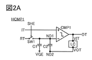
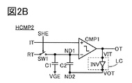
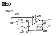
- 2A, 2B, 2C, and 2D are circuit diagrams showing an example of the hysteresis comparator.
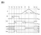
- FIG. 3 is a timing chart showing an operation example of the hysteresis comparator.
- 4A, 4B, 4C, and 4D are circuit diagrams showing an example of the hysteresis comparator.
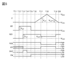
- FIG. 5 is a timing chart showing an operation example of the hysteresis comparator.
- FIG. 6 is a timing chart showing an operation example of the hysteresis comparator.
- FIG. 7 is a block diagram showing an example of a semiconductor device.
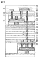
- FIG. 8 is a schematic sectional view illustrating a configuration example of a semiconductor device.
- FIG. 9 is a schematic sectional view illustrating a configuration example of a semiconductor device.
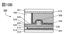
- 10A, 10B, and 10C are schematic cross-sectional views each illustrating a structural example of a transistor.
- 11A and 11B are schematic cross-sectional views each illustrating a structural example of a transistor.
- FIG. 12 is a schematic sectional view illustrating a configuration example of a semiconductor device.
- 13A and 13B are schematic cross-sectional views each illustrating a structural example of a transistor.
- FIG. 14 is a schematic sectional view illustrating a configuration example of a semiconductor device.
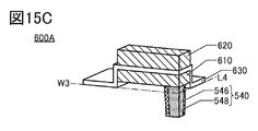
- 15A, 15B, and 15C are a top view and a perspective view showing a configuration example of a capacitor.
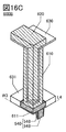
- 16A, 16B, and 16C are a top view and a perspective view showing a configuration example of a capacitor.
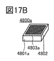
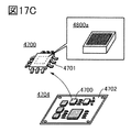
- 17A, 17B, 17C, and 17D are perspective views showing an example of a semiconductor wafer and electronic components.
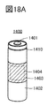
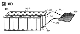
- 18A, 18B, 18C, and 18D are perspective views illustrating an example of a power storage device.
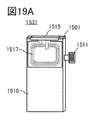
- 19A, 19B, and 19C are perspective views each illustrating an example of a power storage device.
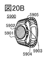
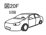
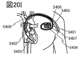
- 20A, 20B, 20C, 20D, 20E, 20F, 20G, 20H, and 20I are perspective views illustrating an example of a product.
- a metal oxide is a metal oxide in a broad sense. Metal oxides are classified into oxide insulators, oxide conductors (including transparent oxide conductors), oxide semiconductors (Oxide Semiconductor or simply OS), and the like.
- the metal oxide when a metal oxide is used for the active layer of a transistor, the metal oxide may be referred to as an oxide semiconductor. That is, when a metal oxide can form a channel formation region of a transistor having at least one of an amplification effect, a rectification effect, and a switching effect, the metal oxide is abbreviated as a metal oxide semiconductor. It can be called OS.
- OS FET or “OS transistor”
- it can be referred to as a transistor including a metal oxide or an oxide semiconductor.
- metal oxides having nitrogen may be collectively referred to as metal oxides. Further, the metal oxide containing nitrogen may be referred to as a metal oxynitride.
- the contents described in one embodiment are different from the contents described in the embodiment (may be a part of the contents) and one or more different embodiments. It is possible to apply, combine, replace, or the like with respect to at least one of the contents described in the form (or a part of the contents).
- Embodiment 1 In this embodiment mode, a semiconductor device which detects when overcharge or overdischarge occurs in one battery and transmits a detection signal will be described. Further, the semiconductor device detects not only one battery but also an assembled battery in which a plurality of batteries (cells) are connected in series, similarly, detecting overcharge or overdischarge in one of the cells. can do.
- the semiconductor device shown in FIG. 1 capable of detecting overcharge or overdischarge of the cell will be described.
- the semiconductor device 100 has a plurality of circuits CNC and a plurality of hysteresis comparators HCMP.
- the semiconductor device 100 has a function of detecting overcharge or overdischarge for each of the plurality of cells CE included in the assembled battery BAT.
- a plurality of cells CE are electrically connected in series in the assembled battery BAT.
- the number of circuit CNCs can be the same as the number of cells CE included in the assembled battery BAT, for example. Further, the number of hysteresis comparators HCMP can be the same as the number of cells CE included in the assembled battery BAT, for example.
- the circuit CNC has, for example, an input terminal CI1, an input terminal CI2, an output terminal CO1, and an output terminal CO2.
- the hysteresis comparator HCMP has, for example, an input terminal IT, a reference potential input terminal RT, and an output terminal OT.
- the positive terminal of the cell CE is electrically connected to the input terminal CI1 of the circuit CNC
- the negative terminal of the cell CE is electrically connected to the input terminal CI2 of the circuit CNC.
- the output terminal CO1 of the circuit CNC is electrically connected to the input terminal IT of the hysteresis comparator HCMP
- the output terminal CO2 of the circuit CNC is electrically connected to the reference potential input terminal RT of the hysteresis comparator HCMP.
- the circuit CNC acquires, for example, the voltage between the positive electrode and the negative electrode of the cell CE and converts the voltage into information (for example, voltage, current, resistance value, etc.) according to the voltage, and a reference of the hysteresis comparator HCMP. It has a function of generating a voltage input to the potential input terminal RT, a function of detecting overdischarge and overcharge in the cell CE from the potential output from the output terminal OT of the hysteresis comparator HCMP. Details of the circuit CNC will be described in the second embodiment.
- the hysteresis comparator HCMP is a kind of comparator, and compares the potential input to the input terminal IT with the reference potential input to the reference potential input terminal RT, and outputs the potential according to the comparison result to the output terminal. It has a function to output from OT.
- a comparator can output a high level potential from an output terminal when the potential input to the input terminal is higher than the reference potential input to the reference potential input terminal, and the input terminal inputs the high level potential.
- a low level potential can be output from the output terminal.
- a high level potential can be output from the output terminal.
- the hysteresis comparator may have, for example, two reference potential input terminals.
- the potential input to the input terminal IT is increased from a sufficiently low potential, the potential input to one reference potential input terminal is used as the reference potential, and the reference potential is input to the input terminal IT.
- the potential input to the other reference potential input terminal is used as the reference potential.
- the potential input to one reference potential input terminal is preferably higher than the potential input to the other reference potential input terminal.
- a hysteresis comparator can be used.
- the overcharge state is set when the cell voltage is higher than the voltage V1, and the high-level side threshold voltage of the hysteresis comparator (may be referred to as high-level reference potential).
- the voltage V1 may be set, and the desired voltage V2 may be set as the low-level side threshold voltage (may be referred to as low-level reference potential) of the hysteresis comparator.
- the voltage V2 can be 4.0V, and more preferably 4.1V.
- the output potential of the hysteresis comparator changes from the high level potential to the low level potential (or the low level potential). Potential to a high level potential).
- a detection signal By detecting the transition of the output potential (hereinafter, sometimes referred to as a detection signal) by a control circuit or the like provided separately, the cell can be detected as an overcharged state, and the cell is charged. You can stop. After that, when the cell discharges, and the voltage of the cell falls below 4.1V, the output potential of the hysteresis comparator should transit from the low level potential to the high level potential (or from the high level potential to the low level potential). become.
- the cell When the voltage of the cell is less than 4.1V, the cell is not in the overcharged state, and thus can be charged. That is, by detecting the transition of the output potential by a separately provided control circuit or the like, the cell can be detected as being in a chargeable state, and the cell can be charged.
- the over-discharge state is set when the cell voltage is lower than the voltage V2, the voltage V2 is set as the low-level side threshold voltage of the hysteresis comparator, and the high-level of the hysteresis comparator is set.
- a desired voltage V1 may be set as the side threshold voltage. At this time, as an example, when the voltage V2 is 2.5V, the voltage V1 can be 3.2V, and more preferably 3.0V.
- the output potential of the hysteresis comparator changes from the high level potential to the low level potential (or low level potential). Potential to a high level potential).
- a detection signal By detecting the transition of the output potential (hereinafter, sometimes referred to as a detection signal) by a control circuit provided separately, the cell can be detected as an overdischarged state, and the discharge of the cell is stopped. can do. After that, when the cell is charged, when the voltage of the cell exceeds 3.0 V, the output potential of the hysteresis comparator transits from the low level potential to the high level potential (or from the high level potential to the low level potential).
- the cell When the voltage of the cell is higher than 3.0V, the cell is not in the over-discharged state, and thus the cell is in the dischargeable state. That is, the transition of the output potential is detected by a separately provided control circuit or the like, whereby the cell can be detected as a dischargeable state, and the cell can be discharged.
- the high-level side threshold voltage and the low-level side threshold voltage of the hysteresis comparator are set for one cell, and the detection signal output from the output terminal of the hysteresis comparator is acquired. , It is possible to know whether overcharge or overdischarge has occurred in the cell. As described above, it is preferable to set the high-level side threshold voltage and the low-level side threshold voltage of the hysteresis comparator according to the overcharge state or the overdischarge state, whichever is desired to be detected. ..
- One aspect of the present invention is a hysteresis comparator made in view of the above, in which the hysteresis comparator has one reference potential input terminal and can be driven by inputting one reference potential.
- FIG. 2A A hysteresis comparator of one aspect of the present invention is shown in Figure 2A.
- the hysteresis comparator HCMP1 has a comparator CMP1, a switch SW1, a capacitor C1, a capacitor C2, and a logic circuit LC.
- the comparator CMP1 has a + side input terminal, a ⁇ side input terminal, and an output terminal.
- the + side input terminal may be paraphrased as one of the first input terminal and the second input terminal
- the ⁇ side input terminal may be paraphrased as the other of the first input terminal and the second input terminal.
- the input terminal IT is electrically connected to the + side input terminal of the comparator CMP1
- the reference potential input terminal RT is electrically connected to the first terminal of the switch SW1
- the output terminal OT is the output terminal of the comparator CMP1.
- And is electrically connected to the terminal VIT of the logic circuit LC.
- the second terminal of the switch SW1 is electrically connected to one of the pair of conductive regions of the capacitor C1, one of the pair of conductive regions of the capacitor C2, and the ⁇ side input terminal of the comparator CMP1.
- the other of the pair of conductive regions of the capacitor C1 is electrically connected to the wiring VGE
- the other of the pair of conductive regions of the capacitor C2 is electrically connected to the terminal VOT of the logic circuit LC.
- connection point is illustrated as a node ND1 (may be referred to as a first potential holding unit), and the electrical connection point between the other of the pair of conductive regions of the capacitor C2 and the terminal VOT of the logic circuit LC is defined as a node ND2 ( It may be referred to as a second potential holding unit.).
- the capacitance values of the capacitors C1 and C2 may be 0.01 fF or more and 100 pF or less, more preferably 0.05 fF or more and 10 pF or less, and further preferably 0.1 fF or more and 1 pF or less.
- the wiring VGE functions as a wiring that gives a constant voltage, for example.
- the constant voltage provided by the wiring VGE can be, for example, a ground potential (GND).
- the potential other than the ground potential (GND) may be a positive potential or a negative potential.
- the logic circuit LC has a terminal VIT and a terminal VOT.
- the logic circuit LC has a function of an inverter circuit, and specifically has a function of outputting an inverted signal of a signal input to the terminal VIT to the terminal VOT. Therefore, the logic circuit LC may include an inverter circuit as an example.
- the hysteresis comparator HCMP2 shown in FIG. 2B has a configuration in which the logic circuit LC included in the hysteresis comparator HCMP1 of FIG. 2A has an inverter circuit INV. Further, the logic circuit LC may be, for example, an inverter circuit, a NAND circuit, a NOR circuit, an XOR circuit, or a circuit combining these.
- the switch SW1 in this specification and the like is turned on when a high-level potential is applied to the control terminal and turned off when a low-level potential is applied to the control terminal. Note that in FIG. 2A, the control terminal of the switch SW1 is electrically connected to the wiring SHE.
- switch SW1 for example, an electrical switch such as an analog switch or a transistor can be applied.
- a mechanical switch such as MEMS (Micro Electro Mechanical Systems) can be applied.
- the hysteresis comparator HCMP3 shown in FIG. 2C has a configuration in which the switch SW1 included in the hysteresis comparator HCMP1 of FIG. 2A is replaced with a transistor TrS1.
- the transistor TrS1 can be, for example, an OS transistor or a transistor including silicon in a channel formation region (hereinafter referred to as a Si transistor).
- the silicon for example, single crystal silicon, amorphous silicon (hydrogenated amorphous silicon), microcrystalline silicon, polycrystalline silicon, or the like can be used.
- the transistors other than the OS transistor and the Si transistor for example, a transistor having a compound semiconductor as an active layer, a transistor having a carbon nanotube as an active layer, a transistor having an organic semiconductor as an active layer, or the like can be used.
- the transistor TrS1 since the transistor TrS1 holds the charge accumulated in the capacitor C1 and the capacitor C2, it is preferable that the off-state current of the transistor TrS1 be low. Therefore, the transistor TrS1 is preferably an OS transistor. In particular, when an OS transistor is used as the transistor TrS1, the OS transistor preferably has the structure of the transistor described in Embodiment 3, in particular.
- a metal oxide contained in a channel formation region is an oxide containing at least one of indium, an element M (the element M includes aluminum, gallium, yttrium, tin, and the like) and zinc. More preferably.
- the off-state current of the OS transistor in which the metal oxide is included in the channel formation region is 10 aA (1 ⁇ 10 ⁇ 17 A) or less per 1 ⁇ m channel width, preferably 1 aA (1 ⁇ 10 ⁇ 18 A) per 1 ⁇ m channel width.
- 10 zA (1 ⁇ 10 ⁇ 20 A) or less per 1 ⁇ m of channel width further preferably 1 zA (1 ⁇ 10 ⁇ 21 A) or less per 1 ⁇ m of channel width, and further preferably 100 yA (1 ⁇ 1 per 1 ⁇ m of channel width). It can be 10 ⁇ 22 A) or less.
- the OS transistor has a low carrier concentration of metal oxide, the off-state current remains low even when the temperature of the OS transistor changes. For example, even when the temperature of the OS transistor is 150° C., the off-state current can be 100 zA per 1 ⁇ m of the channel width.
- the transistor TrS1 included in the hysteresis comparator HCMP3 in FIG. 2C is an n-channel transistor, but it may be a p-channel transistor.
- the transistor TrS1 included in the hysteresis comparator HCMP3 is a single-gate structure transistor, but the transistor TrS1 may be a multi-gate structure n-channel transistor.
- the transistor TrS1 of the hysteresis comparator HCMP4 shown in FIG. 2D has a first gate and a second gate as an n-channel transistor having a multi-gate structure.
- the first gate is described as a gate (may be referred to as a front gate) and the second gate is described as a back gate.
- the second gate can be interchanged with each other. Therefore, in this specification and the like, the phrase “gate” can be replaced with the phrase “backgate”.
- the phrase “back gate” can be interchanged with the phrase “gate”.
- the connection configuration "the gate is electrically connected to the first wiring and the back gate is electrically connected to the second wiring” is "the back gate is electrically connected to the first wiring. And the gate is electrically connected to the second wiring”.
- the hysteresis comparator of one embodiment of the present invention does not depend on the connection configuration of the back gate of the transistor.
- a back gate is illustrated in the transistor TrS1 illustrated in FIG. 2D, and a connection configuration of the back gate is not illustrated, but an electrical connection destination of the back gate can be determined at a design stage. it can.
- the gate and the back gate may be electrically connected in order to increase the on-state current of the transistor. That is, for example, the gate of the transistor TrS1 and the back gate may be electrically connected.
- a wiring electrically connected to an external circuit or the like is provided in order to change the threshold voltage of the transistor or reduce the off-state current of the transistor. Then, a potential may be applied to the back gate of the transistor by the external circuit or the like. Note that this applies not only to FIG. 2D but also to other transistors described in other portions of the specification or other transistors illustrated in other drawings.
- the transistor TrS1 having the back gate for example, the OS transistor described above can be used.
- the transistor is preferably an OS transistor. That is, the comparator CMP1 and/or the logic circuit LC may be a unipolar circuit including OS transistors. Further, the OS transistor included in the comparator CMP1 and/or the logic circuit LC may be a transistor having a multi-gate structure, a transistor having a back gate, or the like.
- an n-type semiconductor in the metal oxide of the semiconductor layer of the OS transistor, an n-type semiconductor can be manufactured using a metal oxide containing indium (eg, In oxide) or a metal oxide containing zinc (eg, Zn oxide).
- transistors with various structures can be used. Therefore, there is no limitation on the type of transistor used.
- a Si transistor a transistor including single crystal silicon, or non-single-crystal typified by amorphous silicon, polycrystalline silicon, microcrystal (also referred to as microcrystal, nanocrystal, semi-amorphous) silicon, or the like is given.
- a transistor having a semiconductor film or the like can be used.
- a thin film transistor (TFT) in which a semiconductor included in the transistor is thinned can be used. There are various advantages when using a TFT.
- the manufacturing apparatus since it can be manufactured at a lower temperature than in the case of single crystal silicon, it is possible to reduce the manufacturing cost or increase the size of the manufacturing apparatus. Since the manufacturing apparatus can be enlarged, it can be manufactured on a large substrate. Therefore, since a large number of display devices can be manufactured at the same time, the manufacturing cost can be reduced.
- the manufacturing temperature is low, a substrate having low heat resistance can be used. Therefore, a transistor can be manufactured over a light-transmitting substrate.
- light transmission through a display element can be controlled by using a transistor over a substrate having a light-transmitting property.
- the transistor since the transistor has a small thickness, part of the film forming the transistor can transmit light. Therefore, the aperture ratio can be improved.
- a compound semiconductor eg, Ge, ZnSe, CdS, GaAs, InP, GaN, SiGe, or the like
- an oxide semiconductor eg, Zn—O, In—Ga—Zn—O, In—
- a transistor including Zn-O, In-Sn-O (ITO), Sn-O, Ti-O, Al-Zn-Sn-O (AZTO), In-Sn-Zn-O, or the like can be used. ..
- a compound semiconductor of these, or a thin film transistor in which these oxide semiconductors are thinned can be used. With these, the manufacturing temperature can be lowered, so that the transistor can be manufactured at room temperature, for example.
- the transistor can be formed directly on a substrate having low heat resistance, such as a plastic substrate or a film substrate.
- a substrate having low heat resistance such as a plastic substrate or a film substrate.
- these compound semiconductors or oxide semiconductors can be used not only for the channel portion of a transistor but also for other purposes.
- these compound semiconductors or oxide semiconductors can be used for wirings, resistance elements, pixel electrodes, light-transmitting electrodes, or the like. Since they can be formed or formed at the same time as the transistor, cost can be reduced.
- a transistor formed by an inkjet method or a printing method can be used. As a result, they can be manufactured at room temperature, at a low degree of vacuum, or on a large substrate. Therefore, manufacturing can be performed without using a mask (reticle), so that the layout of the transistor can be easily changed. Alternatively, since it can be manufactured without using a resist, the material cost can be reduced and the number of steps can be reduced. Alternatively, since the film can be attached only to a necessary portion, the material is not wasted and the cost can be reduced as compared with the manufacturing method of etching after forming the film on the entire surface.
- a transistor having an organic semiconductor or a carbon nanotube, or the like can be used as an example of the transistor. With these, a transistor can be formed over a bendable substrate. A device using a transistor including an organic semiconductor or a carbon nanotube can be resistant to shock.
- a transistor including a layered substance that functions as a semiconductor can be used.
- the layered substance is a general term for a group of materials having a layered crystal structure.
- the layered crystal structure is a structure in which layers formed by a covalent bond or an ionic bond are stacked via a bond weaker than the covalent bond or the ionic bond, such as van der Waals force.
- the layered material has high electric conductivity in the unit layer, that is, high two-dimensional electric conductivity.
- Examples of the layered substance include graphene, silicene, chalcogenide and the like.
- a chalcogenide is a compound containing chalcogen.
- chalcogen is a general term for elements belonging to Group 16 and includes oxygen, sulfur, selenium, tellurium, polonium, and livermolium.
- Examples of chalcogenides include transition metal chalcogenides and group 13 chalcogenides.
- a transition metal chalcogenide that functions as a semiconductor can be used as an example of a transistor.
- the transition metal chalcogenide include molybdenum sulfide (typically MoS 2 ), molybdenum selenide (typically MoSe 2 ), molybdenum tellurium (typically MoTe 2 ), and tungsten sulfide (typically).
- WS 2 tungsten selenide
- WSe 2 tungsten tellurium
- WTe 2 hafnium sulfide
- hafnium selenide typically HfSe 2
- hafnium selenide typically HfSe 2
- Zirconium sulfide typically ZrS 2
- zirconium selenide typically ZrSe 2
- transistors having various structures can be used as the transistor.
- a MOS transistor, a junction transistor, a bipolar transistor, or the like can be used as the transistor.
- MOS transistor the size of the transistor can be reduced. Therefore, a large number of transistors can be mounted.
- bipolar transistor a large amount of current can flow. Therefore, the circuit can be operated at high speed.
- the MOS type transistor and the bipolar transistor may be formed in a mixed manner on one substrate. As a result, low power consumption, miniaturization, high speed operation, etc. can be realized.
- a transistor having a structure in which gate electrodes are provided above and below an active layer can be applied.
- the gate electrodes With the structure in which the gate electrodes are arranged above and below the active layer, a circuit configuration in which a plurality of transistors are connected in parallel is obtained. Therefore, since the channel formation region is increased, the current value can be increased.
- a structure in which the gate electrodes are provided above and below the active layer facilitates formation of a depletion layer, so that the S value can be improved.
- examples of transistors include a structure in which a gate electrode is provided over an active layer, a structure in which a gate electrode is provided under an active layer, a positive stagger structure, an inverted stagger structure, and a plurality of channel regions.
- a transistor having a divided structure, a structure in which active layers are connected in parallel, or a structure in which active layers are connected in series can be used.
- a planar type, a FIN type (fin type), a TRI-GATE type (tri-gate type), a top gate type, a bottom gate type, a double gate type (gates are arranged above and below a channel), and the like are used. , Can take various configurations.
- a transistor having a structure in which a source electrode and a drain electrode overlap with an active layer (or part thereof) can be used.
- the structure in which the source electrode and the drain electrode overlap with the active layer (or part thereof) it is possible to prevent the operation from becoming unstable due to the accumulation of charges in part of the active layer.
- a structure provided with an LDD region can be applied.
- the LDD region By providing the LDD region, off current can be reduced or the withstand voltage of the transistor can be improved (improvement in reliability).
- the drain current when operating in the saturation region, the drain current does not change so much even if the voltage between the drain and the source changes, and voltage/current characteristics with a flat slope can be obtained. it can.
- a transistor can be formed using various substrates.
- the type of substrate is not limited to a particular type.
- the substrate include a semiconductor substrate (for example, a single crystal substrate or a silicon substrate), an SOI substrate, a glass substrate, a quartz substrate, a plastic substrate, a sapphire glass substrate, a metal substrate, a stainless steel substrate, and a stainless steel foil.
- glass substrates include barium borosilicate glass, aluminoborosilicate glass, and soda lime glass.
- Examples of the flexible substrate, the laminated film, the base film and the like include the following.
- plastics represented by polyethylene terephthalate (PET), polyethylene naphthalate (PEN), polyether sulfone (PES), and polytetrafluoroethylene (PTFE).
- PET polyethylene terephthalate
- PEN polyethylene naphthalate
- PES polyether sulfone
- PTFE polytetrafluoroethylene
- a synthetic resin such as acrylic resin.
- polypropylene, polyester, polyvinyl fluoride, polyvinyl chloride, or the like is used.
- polyamide, polyimide, aramid, epoxy resin, an inorganic vapor deposition film, paper, or the like can be given.
- a transistor using a semiconductor substrate, a single crystal substrate, an SOI substrate, or the like, a transistor with small variation in characteristics, size, shape, or the like, high current capability, and small size can be manufactured. ..
- a circuit is formed using such transistors, low power consumption of the circuit or high integration of the circuit can be achieved.
- a flexible substrate may be used as the substrate, and the transistor may be formed directly on the flexible substrate.
- a separation layer may be provided between the substrate and the transistor.
- the peeling layer can be used for separating a semiconductor device over a part of the semiconductor layer, separating the semiconductor layer from the substrate, and transferring the semiconductor device to another substrate. At that time, the transistor can be transferred to a substrate having poor heat resistance or a flexible substrate.
- a structure having a laminated structure of an inorganic film of a tungsten film and a silicon oxide film, a structure in which an organic resin film such as polyimide is formed on a substrate, or the like can be used.
- a transistor may be formed using one substrate, and then the transistor may be transferred to another substrate and the transistor may be placed on another substrate.
- a substrate on which a transistor is transferred in addition to a substrate on which the above transistor can be formed, a paper substrate, a cellophane substrate, an aramid film substrate, a polyimide film substrate, a stone substrate, a wood substrate, a cloth substrate (natural fiber) (Including silk, cotton, hemp), synthetic fiber (nylon, polyurethane, polyester) or recycled fiber (acetate, cupra, rayon, recycled polyester, etc.), leather substrate, or rubber substrate.
- the cost can be reduced by reducing the number of components, or the reliability can be improved by reducing the number of connection points with circuit components.
- a part of the circuit necessary for realizing the predetermined function is formed over one substrate and another part of the circuit necessary for realizing the predetermined function is formed over another substrate. It is possible. For example, a part of a circuit necessary for realizing a predetermined function is formed over a glass substrate and another part of a circuit necessary for realizing the predetermined function is a single crystal substrate (or an SOI substrate). Can be formed into. Then, a single crystal substrate (also referred to as an IC chip) on which another part of the circuit necessary for realizing a predetermined function is formed is connected to the glass substrate by COG (Chip On Glass), and the glass substrate is connected.
- COG Chip On Glass
- the IC chip can be placed in the.
- the IC chip can be connected to the glass substrate using TAB (Tape Automated Bonding), COF (Chip On Film), SMT (Surface Mount Technology), or a printed circuit board.
- TAB Transmission Automated Bonding
- COF Chip On Film
- SMT Surface Mount Technology
- part of the circuit is formed over the same substrate as the pixel portion, so that cost can be reduced by reducing the number of components or reliability can be improved by reducing the number of connection points with circuit components. ..
- the power consumption of a circuit having a high driving voltage or a circuit having a high driving frequency is often high. Therefore, such a circuit is formed over a substrate (for example, a single crystal substrate) different from the pixel portion to form an IC chip. By using this IC chip, it is possible to prevent an increase in power consumption.
- 3A and 3B show a voltage input to the input terminal IT, a voltage input to the reference potential input terminal RT, a voltage output from the output terminal OT, and a wiring SHE between time T1 and time T10.
- 6 is a timing chart showing variations of the voltage input to the node, and the potentials of the node ND1 and the node ND2. Note that high in FIG. 3 indicates a high level potential and low indicates a low level potential.
- V GND is input to the input terminal IT and the reference potential input terminal RT. Further, a low-level potential is input to the wiring SHE.
- V GND can be, for example, ground potential. Further, V GND can be, for example, a reference potential lower or higher than the ground potential.
- the voltage output from the output terminal OT is indefinite. Therefore, the potential of the node ND2 also becomes uncertain. Note that in the timing chart of FIG. 3, the potentials of the output terminal OT and the node ND2 before the time T1 and between the time T1 and the time T3 are hatched.
- the low-level potential is input to the wiring SHE.
- the low-level potential is input to the control terminal of the switch SW1, and the switch SW1 is turned off.
- the switch SW1 is turned off, the reference potential input terminal RT and the ⁇ side input terminal of the comparator CMP1 are brought into a non-conduction state, so that the reference potential input terminal RT is provided between time T1 and time T2.
- the electric potential input to is not input to the-side input terminal (node ND1) of the comparator CMP1.
- V ref1 is input to the reference potential input terminal RT.
- V ref1 can be set to a potential higher than V GND , for example. Since the switch SW1 is in the off state from the time T2 to the time T3, the potential of the-side input terminal (node ND1) of the comparator CMP1 does not change.
- a high-level potential is input to the wiring SHE.
- the high-level potential is input to the control terminal of the switch SW1, and the switch SW1 is turned on.
- the switch SW1 is turned on, the reference potential input terminal RT and the ⁇ side input terminal of the comparator CMP1 are brought into conduction, so that the potential of the ⁇ side input terminal (node ND1) of the comparator CMP1 becomes V. It becomes ref1 .
- V GND is input to the + side input terminal of the comparator CMP1 and V ref1 is input to the ⁇ side input terminal thereof, a low level potential is output from the output terminal of the comparator CMP1. That is, a low level potential is output from the output terminal OT. Further, since the low-level potential is input to the terminal VIT of the logic circuit LC, the high-level potential is output from the terminal VOT of the logic circuit LC. Therefore, the potential of the other (node ND2) of the pair of conductive regions of the capacitor C2 becomes a high-level potential.
- the low-level potential is input to the wiring SHE.
- the low-level potential is input to the control terminal of the switch SW1, and the switch SW1 is turned off.
- the switch SW1 is turned off, the reference potential input terminal RT and the ⁇ side input terminal of the comparator CMP1 are brought out of conduction.
- the power supply potential is not applied to the-side input terminal (node ND1) from the inside of the comparator CMP1, the node ND1 becomes electrically floating. Therefore, the potential V ref1 of the ⁇ side input terminal (node ND1) of the comparator CMP1 is held by one of the pair of conductive regions of the capacitance C1 and the capacitance C2.
- V MAX has a higher potential than V ref1 .
- the + side input of the comparator CMP1 is higher than the potential of the ⁇ side input terminal (node ND1) of the comparator CMP1. Since the potential input to the terminal (potential input from the input terminal IT) becomes high, a high level potential is output from the output terminal of the comparator CMP1. That is, a high level potential is output from the output terminal OT.
- the potential of the other of the pair of conductive regions of the capacitor C2 becomes a low-level potential. Since the node ND1 is in an electrically floating state, at this time, the variation amount of the potential of the other (node ND2) of the pair of conductive regions of the capacitor C2 and the electrostatic capacitances of the capacitors C1 and C2. And the potential of the-side input terminal (node ND1) of the comparator CMP1 changes. In the present operation example, it is assumed that this causes the potential of the ⁇ side input terminal (node ND1) of the comparator CMP1 to change from V ref1 to V ref2 .
- the high-level potential of the other (node ND2) of the pair of conductive regions of the capacitor C2 between time T3 and time T7 is set to V H
- 1 of the capacitor C2 between time T7 and time T8 is set.
- the potential input from the input terminal IT decreases from V MAX to V GND with time. That is, from time T8 to time T10, the potential input to the + side input terminal of the comparator CMP1 decreases to V GND with the lapse of time.
- the potential of the comparator CMP1 is higher than that of the ⁇ side input terminal (node ND1) of the comparator CMP1 between time T9 and time T10. Since the potential input to the side input terminal (potential input from the input terminal IT) becomes low, a low level potential is output from the output terminal of the comparator CMP1. That is, a low level potential is output from the output terminal OT.
- the potential of the other (node ND2) of the pair of conductive regions of the capacitor C2 becomes a high-level potential. Since the node ND1 is in an electrically floating state, at this time, the variation amount of the potential of the other (node ND2) of the pair of conductive regions of the capacitance C2 and the capacitance values of the capacitances C1 and C2. The potential of the-side input terminal (node ND1) of the comparator CMP1 changes accordingly.
- the potential of the other (node ND2) of the pair of conductive regions of the capacitor C2 from time T9 to time T10 is the other of the pair of conductive regions of the capacitor C2 from time T6 to time T7. Since the potential is the same high level potential as the (node ND2), the potential of the ⁇ side input terminal (node ND1) of the comparator CMP1 from time T9 to time T10 is V ref1 .
- a hysteresis comparator having a hysteresis width of V ref1 ⁇ V ref2 can be realized.
- the hysteresis width of the hysteresis comparator HCMP1 can be determined from the equation (E1) by determining the respective capacitance values C 1 and C 2 of the capacitance C1 and the capacitance C2. it can. For example, when each of the capacitance values C 1 and C 2 is 0.1 fF, the hysteresis width is (V H ⁇ V L )/2. In addition, for example, when the capacitance values C 1 and C 2 are 0.3 fF and 0.1 fF, respectively, the hysteresis width is (V H ⁇ V L )/4.
- One embodiment of the present invention is not limited to the hysteresis comparators HCMP1 to HCMP4 illustrated in FIGS. 2A to 2D. Depending on the situation, the configuration of any one of the hysteresis comparators HCMP1 to HCMP4 may be changed.
- the logic circuit LC may have a NAND circuit.
- the hysteresis comparator HCMP5 shown in FIG. 4A has a configuration in which the terminal VIT is the first input terminal of the NAND circuit LCNA and the terminal VOT is the output terminal of the NAND circuit LCNA in the hysteresis comparator HCMP1 of FIG. 2A.
- the wiring EN is electrically connected to the second input terminal of the NAND circuit LCNA.
- the wiring EN functions as a wiring that gives a high-level potential or a low-level potential, for example.
- FIG. 5 shows the voltage input to the input terminal IT, the voltage input to the reference potential input terminal RT, the voltage output from the output terminal OT, and the wiring SHE from time T11 to time T20 and in the vicinity thereof.
- 6 is a timing chart showing variations of the voltage input to the node, the voltage input to the wiring EN, and the potentials of the node ND1 and the node ND2.
- high shown in FIG. 5 indicates a high-level potential
- low indicates a low-level potential.
- V GND is input to the input terminal IT and the reference potential input terminal RT. Further, a low-level potential is input to the wiring SHE.
- V GND the description of the description of V GND described in Operation Example 1 is referred to.
- a high level potential is output from the output terminal.
- the low-level potential is input to the second terminal of the NAND circuit LCNA and the high-level potential is output from the output terminal of the NAND circuit LCNA. The electric potential is output.
- the output terminal OT is electrically connected to the first terminal of the NAND circuit LCNA, but since the low-level potential is input to the second terminal of the NAND circuit LCNA, it is output from the output terminal of the NAND circuit LCNA.
- the applied voltage does not depend on the voltage input to the first terminal of the NAND circuit LCNA.
- the voltage output from the output terminal OT is indefinite between time T11 and time T13, and the potential of the output terminal OT is hatched in the timing chart of FIG.
- the low-level potential is input to the wiring SHE.
- the low-level potential is input to the control terminal of the switch SW1, and the switch SW1 is turned off.
- the switch SW1 is turned off, the reference potential input terminal RT and the ⁇ side input terminal of the comparator CMP1 are brought into a non-conduction state, so that the reference potential input terminal RT is from time T11 to time T12.
- the electric potential input to is not input to the-side input terminal (node ND1) of the comparator CMP1.
- V ref1 is input to the reference potential input terminal RT.
- V ref1 can be set to a potential higher than V GND , for example. Since the switch SW1 is in the off state from time T12 to time T13, the potential of the-side input terminal (node ND1) of the comparator CMP1 does not change.
- the high-level potential is input to the wiring SHE.
- the high-level potential is input to the control terminal of the switch SW1, and the switch SW1 is turned on.
- the switch SW1 is turned on, the reference potential input terminal RT and the ⁇ side input terminal of the comparator CMP1 are brought into conduction, so that the potential of the ⁇ side input terminal (node ND1) of the comparator CMP1 becomes V. It becomes ref1 .
- V GND is input to the + side input terminal of the comparator CMP1 and V ref1 is input to the ⁇ side input terminal thereof, a low level potential is output from the output terminal of the comparator CMP1. That is, a low level potential is output from the output terminal OT. Further, the low-level potential is input to the first terminal of the NAND circuit LCNA, but the high-level potential is continuously output from the output terminal of the NAND circuit LCNA before the time T13.
- the low-level potential is input to the wiring SHE.
- the low-level potential is input to the control terminal of the switch SW1, and the switch SW1 is turned off.
- the switch SW1 is turned off, the reference potential input terminal RT and the ⁇ side input terminal of the comparator CMP1 are brought out of conduction.
- the power supply potential is not applied to the-side input terminal (node ND1) from the inside of the comparator CMP1, the node ND1 becomes electrically floating. Therefore, the potential V ref1 of the ⁇ side input terminal (node ND1) of the comparator CMP1 is held by one of the pair of conductive regions of the capacitance C1 and the capacitance C2.
- the voltage V GND is input to the reference potential input terminal RT. Since the switch SW1 is in the off state from the time T15 to the time T16, the potential of the ⁇ side input terminal (node ND1) of the comparator CMP1 remains unchanged and remains at V ref1 .
- a high-level potential is input to the wiring EN. Since the low-level potential is input to the first terminal of the NAND circuit LCNA, the high-level potential is continuously output from the output terminal of the NAND circuit LCNA before the time T15.
- V MAX has a higher potential than V ref1 .
- the + side input of the comparator CMP1 is higher than the potential of the ⁇ side input terminal (node ND1) of the comparator CMP1. Since the potential input to the terminal (potential input from the input terminal IT) becomes high, a high level potential is output from the output terminal of the comparator CMP1. That is, a high level potential is output from the output terminal OT.
- a high level potential is input to the first terminal of the NAND circuit LCNA. From time T17 to time T18, since the high-level potential is input to the second terminal of the NAND circuit LCNA, the low-level potential is output from the output terminal of the NAND circuit LCNA. Therefore, the potential of the other of the pair of conductive regions of the capacitor C2 (node ND2) becomes a low-level potential. Since the node ND1 is in an electrically floating state, at this time, the variation amount of the potential of the other (node ND2) of the pair of conductive regions of the capacitor C2 and the electrostatic capacitances of the capacitors C1 and C2.
- the potential input from the input terminal IT decreases from V MAX to V GND with time. That is, between time T18 and time T20, the potential input to the + side input terminal of the comparator CMP1 decreases to V GND with the lapse of time.
- the potential of the comparator CMP1 is higher than that of the ⁇ side input terminal (node ND1) of the comparator CMP1 from time T19 to time T20. Since the potential input to the side input terminal (potential input from the input terminal IT) becomes low, a low level potential is output from the output terminal of the comparator CMP1. That is, a low level potential is output from the output terminal OT.
- the high level potential is input to the second terminal of the NAND circuit LCNA, the high level potential is output from the output terminal of the NAND circuit LCNA. Therefore, the potential of the other (node ND2) of the pair of conductive regions of the capacitor C2 becomes a high-level potential. Since the node ND1 is in an electrically floating state, at this time, the variation amount of the potential of the other (node ND2) of the pair of conductive regions of the capacitor C2 and the electrostatic capacitances of the capacitors C1 and C2. And the potential of the-side input terminal (node ND1) of the comparator CMP1 changes.
- the potential of the other (node ND2) of the pair of conductive regions of the capacitor C2 between time T19 and time T20 is the other of the pair of conductive regions of the capacitor C2 between time T16 and time T17. Since it is the same high-level potential as the potential of (node ND2), the potential of the ⁇ side input terminal (node ND1) of the comparator CMP1 from time T19 to time T20 is V ref1 .
- a hysteresis comparator having a hysteresis width of V ref1 ⁇ V ref2 can be realized.
- the hysteresis comparator HCMP6 shown in FIG. 4B is a hysteresis comparator having a configuration different from those shown in FIGS. 2B to 2D and 4A.
- the logic circuit LC has a NOR circuit.
- the terminal VIT is the first input terminal of the NOR circuit LCNO
- the terminal VOT is the output terminal of the NOR circuit LCNO.
- the wiring EN is electrically connected to the second input terminal of the NOR circuit LCNO.
- 6A and 6B show a voltage input to the input terminal IT, a voltage input to the reference potential input terminal RT, a voltage output from the output terminal OT, and a wiring SHE between time T21 and time T30.
- 3 is a timing chart showing variations of the voltage input to the circuit, the voltage input to the wiring EN, and the potentials of the nodes ND1 and ND2. Note that high shown in FIG. 6 indicates a high level potential, and low indicates a low level potential.
- V MAX is input to the input terminal IT and V GND is input to the reference potential input terminal RT. Further, a low-level potential is input to the wiring SHE.
- NOR circuit when a high level potential is input to one of the first terminal and the second terminal, a low level potential is output from the output terminal. From time T21 to time T22, since the high-level potential is input to the wiring EN, the high-level potential is input to the second terminal of the NOR circuit LCNO and the low level is output from the output terminal of the NOR circuit LCNO. The electric potential is output.
- the output terminal OT is electrically connected to the first terminal of the NOR circuit LCNO, since the low-level potential is input to the second terminal of the NOR circuit LCNO, the output terminal OT outputs from the output terminal of the NOR circuit LCNO.
- the applied voltage does not depend on the voltage input to the first terminal of the NOR circuit LCNO.
- the voltage output from the output terminal OT is indefinite between time T21 and time T23, and the potential of the output terminal OT is hatched in the timing chart of FIG.
- a low-level potential is input to the wiring SHE.
- the low-level potential is input to the control terminal of the switch SW1, and the switch SW1 is turned off.
- the switch SW1 is turned off, the reference potential input terminal RT and the ⁇ side input terminal of the comparator CMP1 are brought into a non-conduction state, so that the reference potential input terminal RT is from time T21 to time T22.
- the electric potential input to is not input to the-side input terminal (node ND1) of the comparator CMP1.
- V ref1 is input to the reference potential input terminal RT.
- V ref1 can be, for example, a potential higher than V GND and lower than V MAX . Since the switch SW1 is in the off state from time T22 to time T23, the potential of the-side input terminal (node ND1) of the comparator CMP1 does not change.
- the high-level potential is input to the wiring SHE.
- the high-level potential is input to the control terminal of the switch SW1, and the switch SW1 is turned on.
- the switch SW1 is turned on, the reference potential input terminal RT and the ⁇ side input terminal of the comparator CMP1 are brought into conduction, so that the potential of the ⁇ side input terminal (node ND1) of the comparator CMP1 becomes V. It becomes ref1 .
- V MAX is input to the + side input terminal and V ref1 is input to the ⁇ side input terminal of the comparator CMP1
- a high level potential is output from the output terminal of the comparator CMP1. That is, a high level potential is output from the output terminal OT.
- the high-level potential is input to the first terminal of the NOR circuit LCNO, but the low-level potential is continuously output from the output terminal of the NOR circuit LCNO before the time T23.
- a low-level potential is input to the wiring SHE.
- the low-level potential is input to the control terminal of the switch SW1, and the switch SW1 is turned off.
- the switch SW1 is turned off, the reference potential input terminal RT and the ⁇ side input terminal of the comparator CMP1 are brought out of conduction.
- the power supply potential is not applied to the-side input terminal (node ND1) from the inside of the comparator CMP1, the node ND1 becomes electrically floating. Therefore, the potential V ref1 of the ⁇ side input terminal (node ND1) of the comparator CMP1 is held by one of the pair of conductive regions of the capacitance C1 and the capacitance C2.
- the voltage V GND is input to the reference potential input terminal RT. Since the switch SW1 is in the off state from time T25 to time T26, the potential of the ⁇ side input terminal (node ND1) of the comparator CMP1 does not change and remains at V ref1 .
- a low-level potential is input to the wiring EN from time T25 to time T26. Since the high-level potential is input to the first terminal of the NOR circuit LCNO, the low-level potential is continuously output from the output terminal of the NAND circuit LCNA before the time T25.
- the potential input from the input terminal IT decreases from V MAX to V GND with time. That is, from time T26 to time T28, the potential input to the + side input terminal of the comparator CMP1 decreases to V GND with the lapse of time.
- the potential of the comparator CMP1 is higher than the potential of the ⁇ side input terminal (node ND1) of the comparator CMP1 from time T27 to time T28. Since the potential input to the side input terminal (potential input from the input terminal IT) becomes low, a low level potential is output from the output terminal of the comparator CMP1. That is, a low level potential is output from the output terminal OT.
- the low level potential is input to the first terminal of the NOR circuit LCNO. From time T27 to time T28, since the low-level potential is input to the second terminal of the NOR circuit LCNO, the high-level potential is output from the output end of the NOR circuit LCNO. Therefore, the potential of the other (node ND2) of the pair of conductive regions of the capacitor C2 becomes a high-level potential. Since the node ND1 is in an electrically floating state, at this time, the variation amount of the potential of the other (node ND2) of the pair of conductive regions of the capacitor C2 and the electrostatic capacitances of the capacitors C1 and C2. And the potential of the-side input terminal (node ND1) of the comparator CMP1 changes. In this operation example, the potential of the-side input terminal (node ND1) of the comparator CMP1 changes from V ref1 to V ref3 .
- V ref3 V ref3
- the potential input from the input terminal IT is assumed to increase from V GND to V MAX over time. That is, from time T28 to time T30, the potential input to the + side input terminal of the comparator CMP1 rises to V MAX with time.
- the + side input of the comparator CMP1 is higher than the potential of the ⁇ side input terminal (node ND1) of the comparator CMP1. Since the potential input to the terminal (potential input from the input terminal IT) becomes high, a high level potential is output from the output terminal of the comparator CMP1. That is, a high level potential is output from the output terminal OT.
- the potential of the other of the pair of conductive regions of the capacitor C2 becomes a low-level potential. Since the node ND1 is in an electrically floating state, at this time, depending on the amount of change in the potential of the second terminal (node ND2) of the capacitor C2 and the values of the electrostatic capacitances of the capacitors C1 and C2. Thus, the potential of the-side input terminal (node ND1) of the comparator CMP1 changes.
- the potential of the other (node ND2) of the pair of conductive regions of the capacitor C2 from time T29 to time T30 is the other of the pair of conductive regions of the capacitor C2 from time T26 to time T27. Since it is the same high-level potential as the potential of (node ND2), the potential of the ⁇ side input terminal (node ND1) of the comparator CMP1 from time T29 to time T30 becomes V ref1 .
- a hysteresis comparator having a hysteresis width of V ref3 ⁇ V ref1 can also be realized.
- ⁇ Structure example 4> In the hysteresis comparators HCMP1 to HCMP6 shown in the configuration examples 1 to 3, the + side input terminal is electrically connected to the input terminal IT, and the ⁇ side input terminal is connected to the reference potential via the switch SW1.
- the input terminal RT is electrically connected, one embodiment of the present invention is not limited to this.
- the reference potential input terminal RT is electrically connected to the + side input terminal of the comparator CMP1 through the switch SW1 as in the hysteresis comparator HCMP7 illustrated in FIG.
- the input terminal IT may be electrically connected to the ⁇ side input terminal.
- each of the hysteresis comparators HCMP1 to HCMP7 has a configuration in which a potential according to the potential input to the input terminal IT and the potential of the node ND1 is output from the output terminal OT.
- an output terminal OTB electrically connected to the terminal VOT of the logic circuit LC may be additionally provided as an output terminal as in the hysteresis comparator HCMP8 illustrated in FIG. 4D.
- the hysteresis comparator HCMP8 of FIG. 4D two output terminals OT and OTB are shown, but the hysteresis comparator of one embodiment of the present invention may have only the output terminal OTB as an output terminal.
- any one of the hysteresis comparator HCMP1 to the hysteresis comparator HCMP8 can be configured.
- the hysteresis comparators HCMP1 to HCMP8 can be applied to the semiconductor device having a function of detecting overcharge or overdischarge of the cell CE.
- the semiconductor device can detect overcharge or overdischarge in each of the plurality of cells CE electrically connected in series included in the assembled battery BAT.
- the hysteresis comparators HCMP1 to HCMP8 are It is possible to operate by inputting one constant voltage to the reference potential input terminal. That is, since one constant voltage may be supplied as the reference potential in driving the hysteresis comparators HCMP1 to HCMP8, the area of the voltage generation circuit required to generate the reference potential can be reduced. Also, the hysteresis comparators HCMP1 to HCMP8 can have a smaller circuit area and lower power consumption than the conventional hysteresis comparators.
- FIG. 7 shows a configuration example of the circuit CNC.
- FIG. 7 also illustrates a hysteresis comparator HCMP to which the hysteresis comparators HCMP1 to HCMP8 described in the first embodiment can be applied, and a cell CE.
- FIG. 7 illustrates a circuit CADC as a circuit having a function of controlling discharge and/or charge operations in the cell CE.
- the hysteresis comparator HCMP has the input terminal IT, the reference potential input terminal RT, and the output terminal OT as described in the first embodiment. Further, the hysteresis comparator HCMP has a control terminal SH.
- the control terminal SH is a terminal electrically connected to the wiring SHE in each of the hysteresis comparators HCMP1 to HCMP8 described in Embodiment 1.
- the circuit CNC has a control circuit CTL, a circuit CNV, and a circuit RPG.
- the control circuit CTL is electrically connected to the circuit CNV, the circuit RPG, the control terminal SH and the output terminal OT of the hysteresis comparator HCMP.
- the control circuit CTL may be electrically connected to the output terminal OTB.
- the input terminal CI1 of the circuit CNC is electrically connected to the circuit CNV and the circuit RPG.
- the input terminal CI2 of the circuit CNC is electrically connected to the circuit CNV and the circuit RPG.
- the input terminal CI1 of the circuit CNC is electrically connected to the positive terminal of the cell CE, and the input terminal CI2 of the circuit CNC is electrically connected to the negative terminal of the cell CE. ing. That is, the potential of the positive terminal and the potential of the negative terminal of the cell CE are input to each of the circuit CNV and the circuit RPG.
- the circuit CNV is electrically connected to the output terminal CO1 of the circuit CNC, and the circuit RPG is electrically connected to the output terminal CO2 of the circuit CNC.
- the output terminal CO1 of the circuit CNC is electrically connected to the input terminal IT of the hysteresis comparator HCMP
- the output terminal CO2 of the circuit CNC is the reference potential input terminal RT of the hysteresis comparator HCMP. Is electrically connected to. That is, the circuit CNV is electrically connected to the input terminal IT of the hysteresis comparator HCMP
- the circuit RPG is electrically connected to the reference potential input terminal RT of the hysteresis comparator HCMP.
- the circuit CNV has a function of generating an input voltage to be input to the input terminal IT of the hysteresis comparator HCMP based on the potential of the positive electrode terminal of the cell CE and the potential of the negative electrode terminal, which are input to the circuit CNV. ..
- a conversion circuit such as a voltage dividing circuit, an analog-digital conversion circuit (ADC), a digital-analog conversion circuit (DAC), or a potential level conversion circuit can be applied.
- the circuit CNV may have a function of holding the generated input voltage.
- the circuit RPG is a circuit having a function of generating a reference potential to be input to the reference potential input terminal RT of the hysteresis comparator HCMP.
- the circuit RPG can generate the reference potential based on the potential of the positive electrode terminal and the potential of the negative electrode terminal of the cell CE input to the circuit RPG. That is, the circuit RPG can generate a reference potential according to the cell CE and input the reference potential to the reference potential input terminal of the hysteresis comparator HCMP. Further, the circuit RPG may have a function of holding the generated reference potential.
- the control circuit CTL has a function of acquiring a change in the potential output from the output terminal OT of the hysteresis comparator HCMP and detecting overdischarge or overcharge in the cell CE. Further, when the control circuit CTL detects over-discharge of the cell CE, the control circuit CTL sends a predetermined signal for stopping the discharge operation to the circuit CADC which controls the discharge of the cell CE. May have. Further, when the control circuit CTL detects overcharge in the cell CE, the control circuit CTL has a function of transmitting a predetermined signal for stopping the charging operation to the circuit CADC controlling the charging in the cell CE. You may.
- control circuit CTL may have a function of controlling each of the hysteresis comparator HCMP, the circuit CNV, and the circuit RPG. Specifically, for example, the control circuit CTL applies one of a high level potential and a low level potential to the control terminal SH of the hysteresis comparator HCMP to turn on the switch SW1 (transistor TrS1) included in the hysteresis comparator HCMP, or It can be in one of the off states. In addition, for example, when the semiconductor device 100 is temporarily stopped, the control circuit CTL transmits a predetermined signal to the circuit CNV and the circuit RPG to stop the supply of the power supply voltage to the circuit CNV and the circuit RPG. can do.
- control circuit CTL may have a function of transmitting a control signal for holding the input voltage to the circuit CNV. ..
- control circuit CTL may have a function of transmitting a control signal for holding the reference potential to the circuit RPG. ..
- the semiconductor device 100 uses the reference potential based on the potential of the positive electrode terminal and the potential of the negative electrode terminal of the cell CE, An overcharged state or an overdischarged state of CE can be detected.
- the semiconductor device illustrated in FIG. 8 includes a transistor 300, a transistor 500, and a capacitor 600.
- 10A is a cross-sectional view of the transistor 500 in the channel length direction
- FIG. 10B is a cross-sectional view of the transistor 500 in the channel width direction
- FIG. 10C is a cross-sectional view of the transistor 300 in the channel width direction.
- the transistor 500 is a transistor (OS transistor) having a metal oxide in a channel formation region. Since the transistor 500 has a small off-state current, by using the transistor 500 for a semiconductor device such as the transistor TrS1 of a hysteresis comparator, data written can be held for a long time. That is, the frequency of the refresh operation is low or the refresh operation is not necessary, so that the power consumption of the semiconductor device can be reduced.
- the semiconductor device described in this embodiment includes a transistor 300, a transistor 500, and a capacitor 600 as illustrated in FIG.
- the transistor 500 is provided above the transistor 300
- the capacitor 600 is provided above the transistor 300 and the transistor 500.
- the capacitor 600 can be the hysteresis comparator HCMP, the capacitors C1 and C2 in the hysteresis comparators HCMP1 to HCMP8 described in the above embodiment.
- the transistor 300 is provided over the substrate 311 and includes a conductor 316, an insulator 315, a semiconductor region 313 formed of part of the substrate 311, a low-resistance region 314a serving as a source or drain region, and a low-resistance region 314b. .. Note that the transistor 300 can be applied to, for example, the transistor included in the comparator CMP1 described in the above embodiment.
- a semiconductor substrate for example, a single crystal substrate or a silicon substrate
- the substrate 311 it is preferable to use a semiconductor substrate (for example, a single crystal substrate or a silicon substrate) as the substrate 311.
- the transistor 300 As shown in FIG. 10C, in the transistor 300, the upper surface and the side surface in the channel width direction of the semiconductor region 313 are covered with the conductor 316 with the insulator 315 interposed therebetween. As described above, when the transistor 300 is a Fin type, the effective channel width is increased, so that the on-state characteristics of the transistor 300 can be improved. Further, since the electric field contribution of the gate electrode can be increased, the off characteristics of the transistor 300 can be improved.
- the transistor 300 may be either a p-channel type or an n-channel type.
- a region of the semiconductor region 313 in which a channel is formed, a region in the vicinity thereof, a low-resistance region 314a serving as a source region, a drain region, a low-resistance region 314b, or the like preferably contains a semiconductor such as a silicon-based semiconductor. It preferably includes crystalline silicon. Alternatively, it may be formed of a material having Ge (germanium), SiGe (silicon germanium), GaAs (gallium arsenide), GaAlAs (gallium aluminum arsenide), or the like. A structure may be used in which silicon is used in which the effective mass is controlled by applying stress to the crystal lattice and changing the lattice spacing. Alternatively, the transistor 300 may be a HEMT (High Electron Mobility Transistor) by using GaAs and GaAlAs.
- HEMT High Electron Mobility Transistor
- the low resistance region 314a and the low resistance region 314b in addition to the semiconductor material applied to the semiconductor region 313, impart an n-type conductivity imparting element such as arsenic or phosphorus, or a p-type conductivity imparting boron or the like. Including the element to do.
- the conductor 316 functioning as a gate electrode is a semiconductor material such as silicon, a metal material, or an alloy containing an element imparting n-type conductivity such as arsenic or phosphorus or an element imparting p-type conductivity such as boron.
- a material or a conductive material such as a metal oxide material can be used.
- the threshold voltage of the transistor can be adjusted by selecting the material of the conductor. Specifically, it is preferable to use a material such as titanium nitride or tantalum nitride for the conductor. Further, in order to achieve both conductivity and embedding properties, it is preferable to use a metal material such as tungsten or aluminum as a laminate for the conductor, and it is particularly preferable to use tungsten in terms of heat resistance.
- the transistor 300 illustrated in FIG. 8 is an example, and the structure is not limited thereto, and an appropriate transistor may be used depending on a circuit configuration or a driving method.
- the transistor 300 may have a structure similar to that of the transistor 500 including an oxide semiconductor as illustrated in FIG. Note that details of the transistor 500 will be described later.
- An insulator 320, an insulator 322, an insulator 324, and an insulator 326 are sequentially stacked to cover the transistor 300.
- the insulator 320, the insulator 322, the insulator 324, and the insulator 326 for example, silicon oxide, silicon oxynitride, silicon nitride oxide, silicon nitride, aluminum oxide, aluminum oxynitride, aluminum nitride oxide, aluminum nitride, or the like is used. Good.
- silicon oxynitride refers to a material whose content of oxygen is higher than that of nitrogen as its composition
- silicon oxynitride is a material whose content of nitrogen is higher than that of oxygen as its composition.
- aluminum oxynitride refers to a material having a higher oxygen content than nitrogen as its composition
- aluminum oxynitride as a material having a higher nitrogen content than oxygen as its composition. Indicates.
- the insulator 322 may have a function as a flattening film for flattening a step caused by the transistor 300 and the like provided below the insulator 322.
- the upper surface of the insulator 322 may be flattened by a flattening treatment using a chemical mechanical polishing (CMP) method or the like in order to improve flatness.
- CMP chemical mechanical polishing
- the insulator 324 it is preferable to use a film having a barrier property such that hydrogen and impurities do not diffuse from the substrate 311, the transistor 300, or the like to a region where the transistor 500 is provided.
- a film having a barrier property against hydrogen for example, silicon nitride formed by a CVD method can be used.
- silicon nitride formed by a CVD method when hydrogen is diffused into a semiconductor element including an oxide semiconductor, such as the transistor 500, characteristics of the semiconductor element may be deteriorated in some cases. Therefore, it is preferable to use a film which suppresses diffusion of hydrogen between the transistor 500 and the transistor 300.
- the film that suppresses hydrogen diffusion is a film in which the amount of released hydrogen is small.
- the desorption amount of hydrogen can be analyzed using, for example, a thermal desorption gas analysis method (TDS).
- TDS thermal desorption gas analysis method
- the desorption amount of hydrogen in the insulator 324 is calculated by converting the desorption amount converted into hydrogen atoms into the area of the insulator 324 in the range of the surface temperature of the film from 50° C. to 500° C. Therefore, it may be 10 ⁇ 10 15 atoms/cm 2 or less, preferably 5 ⁇ 10 15 atoms/cm 2 or less.
- the insulator 326 preferably has a lower dielectric constant than the insulator 324.
- the dielectric constant of the insulator 326 is preferably less than 4, and more preferably less than 3.
- the relative dielectric constant of the insulator 326 is preferably 0.7 times or less, and more preferably 0.6 times or less that of the insulator 324.
- a conductor 328, a conductor 330, and the like which are connected to the capacitor 600 or the transistor 500 are embedded.
- the conductor 328 and the conductor 330 have a function as a plug or a wiring.
- the conductor having a function as a plug or a wiring may have a plurality of structures collectively given the same reference numeral. In this specification and the like, the wiring and the plug connected to the wiring may be integrated. That is, part of the conductor may function as a wiring, and part of the conductor may function as a plug.
- a conductive material such as a metal material, an alloy material, a metal nitride material, or a metal oxide material is used in a single layer or a laminated layer. be able to. It is preferable to use a high melting point material such as tungsten or molybdenum, which has both heat resistance and conductivity, and it is preferable to use tungsten. Alternatively, it is preferably formed of a low resistance conductive material such as aluminum or copper. Wiring resistance can be reduced by using a low-resistance conductive material.
- a wiring layer may be provided on the insulator 326 and the conductor 330.
- an insulator 350, an insulator 352, and an insulator 354 are sequentially stacked and provided.
- a conductor 356 is formed over the insulator 350, the insulator 352, and the insulator 354.
- the conductor 356 has a function of a plug connected to the transistor 300 or a wiring. Note that the conductor 356 can be provided using a material similar to that of the conductor 328 and the conductor 330.
- the insulator 350 is preferably an insulator having a barrier property against hydrogen, like the insulator 324.
- the conductor 356 preferably contains a conductor having a barrier property against hydrogen.
- a conductor having a barrier property against hydrogen is formed in the opening portion of the insulator 350 having a barrier property against hydrogen.
- tantalum nitride or the like may be used as the conductor having a barrier property against hydrogen.
- tantalum nitride and tungsten having high conductivity diffusion of hydrogen from the transistor 300 can be suppressed while maintaining conductivity as a wiring.
- the tantalum nitride layer having a hydrogen barrier property is in contact with the insulator 350 having a hydrogen barrier property.
- a wiring layer may be provided on the insulator 354 and the conductor 356.
- an insulator 360, an insulator 362, and an insulator 364 are sequentially stacked and provided.
- a conductor 366 is formed over the insulator 360, the insulator 362, and the insulator 364.
- the conductor 366 has a function as a plug or a wiring. Note that the conductor 366 can be provided using a material similar to that of the conductor 328 and the conductor 330.
- the insulator 360 it is preferable to use an insulator having a barrier property against hydrogen, like the insulator 324.
- the conductor 366 preferably contains a conductor having a barrier property against hydrogen.
- a conductor having a hydrogen barrier property is formed in the opening portion of the insulator 360 having a hydrogen barrier property.
- a wiring layer may be provided on the insulator 364 and the conductor 366.
- an insulator 370, an insulator 372, and an insulator 374 are sequentially stacked and provided.
- a conductor 376 is formed over the insulator 370, the insulator 372, and the insulator 374.
- the conductor 376 has a function as a plug or a wiring. Note that the conductor 376 can be provided using a material similar to that of the conductor 328 and the conductor 330.
- the insulator 370 is preferably an insulator having a barrier property against hydrogen, like the insulator 324.
- the conductor 376 preferably includes a conductor having a barrier property against hydrogen.
- a conductor having a barrier property against hydrogen is formed in the opening portion of the insulator 370 having a barrier property against hydrogen.
- a wiring layer may be provided on the insulator 374 and the conductor 376.
- an insulator 380, an insulator 382, and an insulator 384 are sequentially stacked and provided.
- a conductor 386 is formed over the insulator 380, the insulator 382, and the insulator 384.
- the conductor 386 has a function as a plug or a wiring. Note that the conductor 386 can be provided using a material similar to that of the conductor 328 and the conductor 330.
- the insulator 380 it is preferable to use an insulator having a barrier property against hydrogen, like the insulator 324.
- the conductor 386 preferably contains a conductor having a barrier property against hydrogen.
- a conductor having a hydrogen barrier property is formed in the opening of the insulator 380 having a hydrogen barrier property.
- the semiconductor device has been described above, the semiconductor device according to this embodiment It is not limited to this.
- the number of wiring layers similar to the wiring layer including the conductor 356 may be three or less, or the number of wiring layers similar to the wiring layer including the conductor 356 may be five or more.
- An insulator 510, an insulator 512, an insulator 514, and an insulator 516 are sequentially stacked on the insulator 384. Any of the insulator 510, the insulator 512, the insulator 514, and the insulator 516 is preferably formed using a substance having a barrier property against oxygen and hydrogen.
- insulator 510 and the insulator 514 for example, a film having a barrier property such that hydrogen and impurities do not diffuse from the substrate 311 or the region where the transistor 300 is provided to the region where the transistor 500 is provided is used. Is preferred. Therefore, a material similar to that of the insulator 324 can be used.
- silicon nitride formed by a CVD method can be used as an example of a film having a barrier property against hydrogen.
- silicon nitride formed by a CVD method when hydrogen is diffused into a semiconductor element including an oxide semiconductor, such as the transistor 500, characteristics of the semiconductor element may be deteriorated in some cases. Therefore, it is preferable to use a film which suppresses diffusion of hydrogen between the transistor 500 and the transistor 300.
- the film that suppresses hydrogen diffusion is a film in which the amount of released hydrogen is small.
- a metal oxide such as aluminum oxide, hafnium oxide, or tantalum oxide is preferably used for the insulator 510 and the insulator 514.
- aluminum oxide has a high blocking effect against oxygen and impurities such as hydrogen and water that cause fluctuations in the electrical characteristics of the transistor, which do not pass through the membrane. Therefore, aluminum oxide can prevent impurities such as hydrogen and moisture from entering the transistor 500 during and after the manufacturing process of the transistor. Further, release of oxygen from the oxide included in the transistor 500 can be suppressed. Therefore, it is suitable to be used as a protective film for the transistor 500.
- the same material as that of the insulator 320 can be used for the insulator 512 and the insulator 516. Further, by applying a material having a relatively low dielectric constant to these insulators, it is possible to reduce the parasitic capacitance generated between the wirings.
- a silicon oxide film, a silicon oxynitride film, or the like can be used as the insulator 512 and the insulator 516.
- a conductor 518, a conductor (eg, a conductor 503) included in the transistor 500, and the like are embedded in the insulator 510, the insulator 512, the insulator 514, and the insulator 516.
- the conductor 518 has a function of a plug connected to the capacitor 600 or the transistor 300, or a wiring.
- the conductor 518 can be provided using a material similar to that of the conductor 328 and the conductor 330.
- the conductor 510 in a region in contact with the insulator 510 and the insulator 514 be a conductor having a barrier property against oxygen, hydrogen, and water.
- the transistor 300 and the transistor 500 can be separated by a layer having a barrier property against oxygen, hydrogen, and water, and diffusion of hydrogen from the transistor 300 to the transistor 500 can be suppressed.
- the transistor 500 is provided above the insulator 516.
- the transistor 500 includes a conductor 503 arranged so as to be embedded in an insulator 514 and an insulator 516 and an insulator arranged over the insulator 516 and the conductor 503. 520, an insulator 522 placed over the insulator 520, an insulator 524 placed over the insulator 522, an oxide 530a placed over the insulator 524, and an oxide 530a Between the conductor 542a and the conductor 542b, and the conductor 542a and the conductor 542b that are spaced apart from each other on the oxide 530b, and the conductor 542a and the conductor 542b that are disposed on the conductor 542a and the conductor 542b.
- An insulator 580 having an opening formed so as to overlap with the oxide 530, an oxide 530c arranged on the bottom and side surfaces of the opening, an insulator 550 arranged on the formation surface of the oxide 530c, and a formation surface of the insulator 550. And a conductor 560 arranged.
- an insulator 544 is preferably provided between the oxide 530a, the oxide 530b, the conductor 542a, and the conductor 542b, and the insulator 580.
- the conductor 560 includes a conductor 560a provided inside the insulator 550, a conductor 560b provided so as to be embedded inside the conductor 560a, and It is preferable to have
- an insulator 574 is preferably provided over the insulator 580, the conductor 560, and the insulator 550.
- the oxide 530a, the oxide 530b, and the oxide 530c may be collectively referred to as the oxide 530.
- the transistor 500 has a structure in which three layers of an oxide 530a, an oxide 530b, and an oxide 530c are stacked in a region where a channel is formed and in the vicinity thereof, the present invention is not limited to this. Not a thing. For example, a single layer of the oxide 530b, a two-layer structure of the oxide 530b and the oxide 530a, a two-layer structure of the oxide 530b and the oxide 530c, or a stacked structure of four or more layers may be provided. Further, in the transistor 500, the conductor 560 is illustrated as a stacked structure of two layers, but the present invention is not limited to this.
- the conductor 560 may have a single-layer structure or a stacked structure including three or more layers.
- the transistor 500 illustrated in FIGS. 8 and 10A is an example, and the structure is not limited thereto, and an appropriate transistor may be used depending on a circuit configuration or a driving method.
- the conductor 560 functions as a gate electrode of the transistor, and the conductors 542a and 542b function as a source electrode and a drain electrode, respectively.
- the conductor 560 is formed so as to be embedded in the opening of the insulator 580 and the region between the conductors 542a and 542b.
- the arrangement of the conductor 560, the conductor 542a, and the conductor 542b is selected in a self-aligned manner with respect to the opening of the insulator 580. That is, in the transistor 500, the gate electrode can be arranged in a self-aligned manner between the source electrode and the drain electrode. Therefore, the conductor 560 can be formed without providing a positioning margin, so that the area occupied by the transistor 500 can be reduced. As a result, the semiconductor device can be miniaturized and highly integrated.
- the conductor 560 is formed in a region between the conductor 542a and the conductor 542b in a self-aligned manner, the conductor 560 does not have a region overlapping with the conductor 542a or the conductor 542b. Accordingly, parasitic capacitance formed between the conductor 560 and the conductors 542a and 542b can be reduced. Therefore, the switching speed of the transistor 500 can be improved and high frequency characteristics can be provided.
- the conductor 560 may function as a first gate (also referred to as a top gate) electrode.
- the conductor 503 may function as a second gate (also referred to as a bottom gate) electrode.
- the threshold voltage of the transistor 500 can be controlled by changing the potential applied to the conductor 503 independently of the potential applied to the conductor 560 and without changing the potential.
- the threshold voltage of the transistor 500 can be made higher than 0 V and the off-state current can be reduced. Therefore, applying a negative potential to the conductor 503 can reduce the drain current when the potential applied to the conductor 560 is 0 V, as compared to the case where no potential is applied.
- the conductor 503 is arranged so as to overlap with the oxide 530 and the conductor 560. Thus, when a potential is applied to the conductor 560 and the conductor 503, the electric field generated from the conductor 560 and the electric field generated from the conductor 503 are connected to cover a channel formation region formed in the oxide 530.
- a structure of a transistor that electrically surrounds a channel formation region by an electric field of a first gate electrode and a second gate electrode is referred to as a surrounded channel (S-channel) structure.
- the conductor 503 has the same structure as the conductor 518, and the conductor 503a is formed in contact with the inner walls of the openings of the insulator 514 and the insulator 516, and the conductor 503b is formed further inside.
- the transistor 500 has a structure in which the conductor 503a and the conductor 503b are stacked, the present invention is not limited to this.
- the conductor 503 may have a single-layer structure or a stacked structure including three or more layers.
- the conductor 503a is preferably made of a conductive material having a function of suppressing diffusion of impurities such as hydrogen atoms, hydrogen molecules, water molecules, and copper atoms (the above impurities are difficult to permeate).
- impurities such as hydrogen atoms, hydrogen molecules, water molecules, and copper atoms
- a conductive material having a function of suppressing diffusion of oxygen eg, at least one of oxygen atoms, oxygen molecules, and the like
- the function of suppressing the diffusion of impurities or oxygen is a function of suppressing the diffusion of any one or all of the impurities or oxygen.
- the conductor 503a since the conductor 503a has a function of suppressing diffusion of oxygen, it is possible to prevent the conductor 503b from being oxidized and decreasing in conductivity.
- the conductor 503b is preferably formed using a conductive material having high conductivity, which contains tungsten, copper, or aluminum as its main component. In that case, the conductor 505 is not necessarily provided.
- the conductor 503b is illustrated as a single layer, it may have a laminated structure, for example, a laminate of titanium or titanium nitride and the above conductive material.
- the insulator 520, the insulator 522, and the insulator 524 have a function as a second gate insulating film.
- the insulator 524 which is in contact with the oxide 530, it is preferable to use an insulator containing more oxygen than the oxygen which satisfies the stoichiometric composition. That is, it is preferable that the insulator 524 be formed with an excess oxygen region. By providing such an insulator containing excess oxygen in contact with the oxide 530, oxygen vacancies in the oxide 530 can be reduced and the reliability of the transistor 500 can be improved.
- an oxide material in which part of oxygen is released by heating is preferably used.
- An oxide that desorbs oxygen by heating means that the amount of desorbed oxygen in terms of oxygen atoms is 1.0 ⁇ 10 18 atoms/cm 3 or more, preferably 1 or more by TDS (Thermal Desorption Spectroscopy) analysis.
- the surface temperature of the film during the TDS analysis is preferably 100° C. or higher and 700° C. or lower, or 100° C. or higher and 400° C. or lower.
- any one or more of heat treatment, microwave treatment, and RF treatment may be performed by contacting the oxide having the excess oxygen region with the oxide 530.
- water or hydrogen in the oxide 530 can be removed.
- reactions occur which bonds VoH is disconnected, when other words happening reaction of "V O H ⁇ V O + H", can be dehydrogenated.
- Part of the hydrogen generated at this time may be combined with oxygen and converted into H 2 O, which is removed from the oxide 530 or the insulator in the vicinity of the oxide 530.
- part of hydrogen may be diffused or captured (also referred to as gettering) in the conductors 542a and 542b.
- a device having a power source for generating high-density plasma or a device having a power source for applying RF to the substrate side for the microwave treatment.
- a gas containing oxygen and using high-density plasma high-density oxygen radicals can be generated, and by applying RF to the substrate side, oxygen radicals generated by high-density plasma can be generated.
- the pressure may be 133 Pa or higher, preferably 200 Pa or higher, more preferably 400 Pa or higher.
- oxygen and argon are used, and the oxygen flow rate ratio (O 2 /(O 2 +Ar)) is 50% or less, preferably 10% or more 30 % Or less is recommended.
- heat treatment is preferably performed with the surface of the oxide 530 exposed.
- the heat treatment may be performed at 100 °C to 450 °C inclusive, more preferably 350 °C to 400 °C inclusive, for example.
- the heat treatment is performed in an atmosphere of nitrogen gas or an inert gas, or an atmosphere containing an oxidizing gas in an amount of 10 ppm or higher, 1% or higher, or 10% or higher.
- the heat treatment is preferably performed in an oxygen atmosphere. Accordingly, oxygen can be supplied to the oxide 530 to reduce oxygen vacancies (V 2 O 3 ).
- the heat treatment may be performed under reduced pressure.
- the heat treatment may be performed in an atmosphere containing an oxidizing gas in an amount of 10 ppm or higher, 1% or higher, or 10% or higher in order to supplement desorbed oxygen after the heat treatment is performed in a nitrogen gas or inert gas atmosphere.
- the heat treatment may be performed in an atmosphere containing an oxidizing gas in an amount of 10 ppm or more, 1% or more, or 10% or more, and then continuously performed in a nitrogen gas or inert gas atmosphere.
- the insulator 522 when the insulator 524 has an excess oxygen region, the insulator 522 preferably has a function of suppressing diffusion of oxygen (eg, oxygen atoms, oxygen molecules, and the like) (the above oxygen is difficult to permeate).
- oxygen eg, oxygen atoms, oxygen molecules, and the like
- the insulator 522 has a function of suppressing diffusion of oxygen and impurities, oxygen contained in the oxide 530 does not diffuse to the insulator 520 side, which is preferable.
- the conductor 503 can be prevented from reacting with the insulator 524 and the oxygen contained in the oxide 530.
- the insulator 522 is, for example, aluminum oxide, hafnium oxide, an oxide containing aluminum and hafnium (hafnium aluminate), tantalum oxide, zirconium oxide, lead zirconate titanate (PZT), strontium titanate (SrTiO 3 ), or It is preferable to use an insulator containing a so-called high-k material such as (Ba, Sr)TiO 3 (BST) in a single layer or a laminated layer. As transistors become finer and more highly integrated, thinning of the gate insulating film may cause problems such as leakage current. By using a high-k material for the insulator functioning as a gate insulating film, it is possible to reduce the gate potential during transistor operation while maintaining the physical film thickness.
- a so-called high-k material such as (Ba, Sr)TiO 3 (BST)
- an insulator containing an oxide of one or both of aluminum and hafnium which is an insulating material having a function of suppressing diffusion of impurities and oxygen and the like (oxygen does not easily permeate).
- the insulator containing one or both oxides of aluminum and hafnium it is preferable to use aluminum oxide, hafnium oxide, an oxide containing aluminum and hafnium (hafnium aluminate), or the like.
- the insulator 522 is formed using such a material, the insulator 522 suppresses release of oxygen from the oxide 530 and mixture of impurities such as hydrogen from the peripheral portion of the transistor 500 into the oxide 530. Functions as a layer.
- aluminum oxide, bismuth oxide, germanium oxide, niobium oxide, silicon oxide, titanium oxide, tungsten oxide, yttrium oxide, or zirconium oxide may be added to these insulators.
- these insulators may be nitrided. Silicon oxide, silicon oxynitride, or silicon nitride may be stacked over the above insulator and used.
- the insulator 520 is preferably thermally stable.
- silicon oxide and silicon oxynitride are preferable because they are thermally stable.
- an insulator made of a high-k material and silicon oxide or silicon oxynitride an insulator 520 having a stacked structure which is thermally stable and has a high relative dielectric constant can be obtained.
- the insulator 520, the insulator 522, and the insulator 524 are illustrated as the second gate insulating film having a stacked-layer structure of three layers.
- the gate insulating film may have a single-layer structure, a double-layer structure, or a stacked structure of four or more layers.
- the laminated structure is not limited to the same material, and may be a laminated structure made of different materials.
- the oxide 530 including the channel formation region it is preferable to use a metal oxide which functions as an oxide semiconductor.
- a metal oxide which functions as an oxide semiconductor.
- the oxide 530 an In-M-Zn oxide (the element M is aluminum, gallium, yttrium, copper, vanadium, beryllium, boron, titanium, iron, nickel, germanium, zirconium, molybdenum, lanthanum, cerium, neodymium). It is preferable to use a metal oxide such as one or more selected from hafnium, tantalum, tungsten, magnesium, and the like.
- the In-M-Zn oxide that can be used as the oxide 530 is preferably a CAAC-OS (C-Axis Aligned Crystalline Oxide Semiconductor) or a CAC-OS (Clu-Aligned Composite Oxide Semiconductor).
- a CAAC-OS C-Axis Aligned Crystalline Oxide Semiconductor
- CAC-OS Clu-Aligned Composite Oxide Semiconductor
- an In—Ga oxide or an In—Zn oxide may be used as the oxide 530.
- a metal oxide having a low carrier concentration for the transistor 500 it is preferable to use a metal oxide having a low carrier concentration for the transistor 500.
- the concentration of impurities in the metal oxide may be lowered and the density of defect states may be lowered.
- low impurity concentration and low defect level density are referred to as high-purity intrinsic or substantially high-purity intrinsic.
- the impurities in the metal oxide include, for example, hydrogen, nitrogen, alkali metals, alkaline earth metals, iron, nickel, silicon and the like.
- hydrogen contained in a metal oxide reacts with oxygen bonded to a metal atom to be water, which may cause oxygen vacancies in the metal oxide.
- oxygen vacancies and hydrogen combine to form a V O H.
- V O H acts as a donor, sometimes electrons serving as carriers are generated.
- part of hydrogen may be bonded to oxygen which is bonded to a metal atom to generate an electron which is a carrier. Therefore, a transistor including a metal oxide containing a large amount of hydrogen is likely to have normally-on characteristics.
- the metal oxide easily moves due to stress such as heat and an electric field; therefore, when a large amount of hydrogen is contained in the metal oxide, reliability of the transistor might be deteriorated.
- the highly purified intrinsic or substantially highly purified intrinsic it is preferable that the highly purified intrinsic or substantially highly purified intrinsic.
- the impurities such as hydrogen (dehydration, may be described as dehydrogenation.)
- oxygenation treatment it is important to supply oxygen to the metal oxide to fill oxygen vacancies (sometimes referred to as oxygenation treatment).
- the metal oxide impurities is sufficiently reduced such V O H By using the channel formation region of the transistor, it is possible to have stable electrical characteristics.
- Deficiency in which hydrogen is contained in oxygen vacancies can function as a metal oxide donor.
- the metal oxide may be evaluated not by the donor concentration but by the carrier concentration. Therefore, in this specification and the like, a carrier concentration which is assumed to be a state where an electric field is not applied is sometimes used as a parameter of a metal oxide, instead of a donor concentration. That is, the “carrier concentration” described in this specification and the like can be called the “donor concentration” in some cases.
- the hydrogen concentration obtained by secondary ion mass spectrometry is less than 1 ⁇ 10 20 atoms/cm 3 , preferably 1 ⁇ 10 19 atoms/cm 3. It is less than 3 , more preferably less than 5 ⁇ 10 18 atoms/cm 3 , and even more preferably less than 1 ⁇ 10 18 atoms/cm 3 .
- the metal oxide has a high bandgap, is an intrinsic (also referred to as I-type) semiconductor, or is a substantially intrinsic semiconductor, and has a channel formation region.
- the carrier concentration of the metal oxide is preferably less than 1 ⁇ 10 18 cm ⁇ 3 , more preferably less than 1 ⁇ 10 17 cm ⁇ 3 , further preferably less than 1 ⁇ 10 16 cm ⁇ 3. It is preferably less than 1 ⁇ 10 13 cm ⁇ 3 , more preferably less than 1 ⁇ 10 12 cm ⁇ 3 .
- the lower limit of the carrier concentration of the metal oxide in the channel formation region is not particularly limited, but can be set to, for example, 1 ⁇ 10 ⁇ 9 cm ⁇ 3 .
- oxygen in the oxide 530 is diffused to the conductor 542a and the conductor 542b,
- the 542a and the conductor 542b may be oxidized. Oxidation of the conductors 542a and 542b is likely to reduce the conductivity of the conductors 542a and 542b. Note that diffusion of oxygen in the oxide 530 to the conductor 542a and the conductor 542b can be restated as absorption of oxygen in the oxide 530 by the conductor 542a and the conductor 542b.
- the oxide 530 diffuses to the conductors 542a and 542b, so that different layers are formed between the conductor 542a and the oxide 530b and between the conductor 542b and the oxide 530b. May be done. Since the different layer contains more oxygen than the conductor 542a and the conductor 542b, it is estimated that the different layer has an insulating property.
- the three-layer structure of the conductor 542a or the conductor 542b, the different layer, and the oxide 530b can be regarded as a three-layer structure including metal-insulator-semiconductor, and MIS (Metal-Insulator-). It may be referred to as a "Semiconductor structure" or a diode junction structure mainly composed of a MIS structure.
- the different layer is not limited to being formed between the conductor 542a and the conductor 542b and the oxide 530b; for example, the different layer may be formed between the conductor 542a and the conductor 542b and the oxide 530c. In some cases, in some cases, between the conductor 542a and the conductor 542b and the oxide 530b, and between the conductor 542a and the conductor 542b and the oxide 530c.
- the metal oxide functioning as a channel formation region in the oxide 530 it is preferable to use a metal oxide having a bandgap of 2 eV or more, preferably 2.5 eV or more. By using a metal oxide having a wide band gap in this manner, off-state current of the transistor can be reduced.
- the oxide 530 has the oxide 530a below the oxide 530b, diffusion of impurities from the structure formed below the oxide 530a into the oxide 530b can be suppressed. Further, by including the oxide 530c over the oxide 530b, diffusion of impurities into the oxide 530b from a structure formed above the oxide 530c can be suppressed.
- the oxide 530 preferably has a stacked structure of a plurality of oxide layers in which the atomic ratio of each metal atom is different.
- the atomic number ratio of the element M in the constituent elements is higher than the atomic number ratio of the element M in the constituent elements in the metal oxide used for the oxide 530b. It is preferable.
- the atomic ratio of the element M to In is preferably higher than the atomic ratio of the element M to In in the metal oxide used for the oxide 530b.
- the atomic ratio of In to the element M is preferably higher than the atomic ratio of In to the element M in the metal oxide used for the oxide 530a.
- a metal oxide that can be used for the oxide 530a or the oxide 530b can be used.
- laminated structure of gallium oxide and In:Ga:Zn 4:2:3 [atomic ratio].
- the energy at the bottom of the conduction band of the oxide 530a and the oxide 530c be higher than the energy at the bottom of the conduction band of the oxide 530b.
- the electron affinity of the oxide 530a and the oxide 530c be smaller than the electron affinity of the oxide 530b.
- the energy level at the bottom of the conduction band changes gently at the junction of the oxide 530a, the oxide 530b, and the oxide 530c.
- the energy level at the bottom of the conduction band at the junction of the oxide 530a, the oxide 530b, and the oxide 530c is continuously changed or continuously joined.
- the density of defect states in the mixed layer formed at the interface between the oxide 530a and the oxide 530b and the interface between the oxide 530b and the oxide 530c is preferably low.
- the oxide 530a and the oxide 530b, and the oxide 530b and the oxide 530c have a common element other than oxygen (as a main component) to form a mixed layer with low defect level density.
- the oxide 530b is an In—Ga—Zn oxide, In—Ga—Zn oxide, Ga—Zn oxide, gallium oxide, or the like may be used as the oxide 530a and the oxide 530c.
- the main carrier path is the oxide 530b.
- the oxide 530a and the oxide 530c having the above structure, the density of defect states in the interface between the oxide 530a and the oxide 530b and the interface between the oxide 530b and the oxide 530c can be reduced. Therefore, the influence of interface scattering on carrier conduction is reduced and the transistor 500 can have high on-state current.
- the conductor 542a and the conductor 542b which function as a source electrode and a drain electrode are provided over the oxide 530b.
- Examples of the conductor 542a and the conductor 542b are aluminum, chromium, copper, silver, gold, platinum, tantalum, nickel, titanium, molybdenum, tungsten, hafnium, vanadium, niobium, manganese, magnesium, zirconium, beryllium, indium, and ruthenium. It is preferable to use a metal element selected from iridium, strontium, and lanthanum, an alloy containing the above metal element as a component, an alloy in which the above metal elements are combined, or the like.
- tantalum nitride, titanium nitride, tungsten, nitride containing titanium and aluminum, nitride containing tantalum and aluminum, ruthenium oxide, ruthenium nitride, oxide containing strontium and ruthenium, oxide containing lanthanum and nickel, and the like are used.
- tantalum nitride, titanium nitride, nitride containing titanium and aluminum, nitride containing tantalum and aluminum, ruthenium oxide, ruthenium nitride, oxide containing strontium and ruthenium, and oxide containing lanthanum and nickel are difficult to oxidize. It is preferable because it is a conductive material or a material that maintains conductivity even when absorbing oxygen. Further, a metal nitride film such as tantalum nitride is preferable because it has a barrier property against hydrogen or oxygen.
- the conductor 542a and the conductor 542b are shown as a single layer structure, but may be a laminated structure of two or more layers.
- a tantalum nitride film and a tungsten film may be stacked.
- a titanium film and an aluminum film may be stacked.
- a two-layer structure in which an aluminum film is stacked over a tungsten film a two-layer structure in which a copper film is stacked over a copper-magnesium-aluminum alloy film, a two-layer structure in which a copper film is stacked over a titanium film, and a tungsten film is formed over the tungsten film.
- a two-layer structure in which copper films are laminated may be used.
- a titanium film or a titanium nitride film a three-layer structure in which an aluminum film or a copper film is stacked over the titanium film or the titanium nitride film, and a titanium film or a titanium nitride film is further formed thereover, a molybdenum film, or
- a molybdenum nitride film and an aluminum film or a copper film are stacked over the molybdenum film or the molybdenum nitride film, and a molybdenum film or a molybdenum nitride film is formed thereover.
- a transparent conductive material containing indium oxide, tin oxide, or zinc oxide may be used.
- regions 543a and 543b may be formed as low resistance regions at the interface of the oxide 530 with the conductor 542a (conductor 542b) and in the vicinity thereof.
- the region 543a functions as one of the source region and the drain region
- the region 543b functions as the other of the source region and the drain region.
- a channel formation region is formed in a region between the region 543a and the region 543b.
- the oxygen concentration in the region 543a (region 543b) may be reduced.
- a metal compound layer containing a metal contained in the conductor 542a (conductor 542b) and a component of the oxide 530 may be formed in the region 543a (region 543b). In such a case, the carrier concentration of the region 543a (region 543b) increases, and the region 543a (region 543b) becomes a low resistance region.
- the insulator 544 is provided so as to cover the conductors 542a and 542b and suppresses oxidation of the conductors 542a and 542b. At this time, the insulator 544 may be provided so as to cover a side surface of the oxide 530 and be in contact with the insulator 524.
- the insulator 544 one kind or two or more kinds of metal oxides selected from hafnium, aluminum, gallium, yttrium, zirconium, tungsten, titanium, tantalum, nickel, germanium, neodymium, lanthanum, magnesium, or the like is used. Can be used. Alternatively, as the insulator 544, silicon nitride oxide, silicon nitride, or the like can be used.
- the insulator 544 it is preferable to use an oxide containing one or both of aluminum and hafnium, such as aluminum oxide, hafnium oxide, aluminum, or an oxide containing hafnium (hafnium aluminate). ..
- hafnium aluminate has higher heat resistance than a hafnium oxide film. Therefore, crystallization is less likely to occur in heat treatment in a later step, which is preferable.
- the insulator 544 is not an essential component if the conductors 542a and 542b are materials having oxidation resistance or if the conductivity does not significantly decrease even when oxygen is absorbed. It may be appropriately designed depending on the desired transistor characteristics.
- impurities such as water and hydrogen contained in the insulator 580 can be suppressed from diffusing into the oxide 530b through the oxide 530c and the insulator 550.
- oxidation of the conductor 560 due to excess oxygen in the insulator 580 can be suppressed.
- the insulator 550 functions as a first gate insulating film.
- the insulator 550 is preferably arranged in contact with the inside (top surface and side surface) of the oxide 530c.
- the insulator 550 is preferably formed using an insulator that contains excess oxygen and releases oxygen by heating.
- silicon oxide containing excess oxygen, silicon oxynitride, silicon nitride oxide, silicon nitride, silicon oxide containing fluorine, silicon oxide containing carbon, carbon oxide containing silicon and nitrogen, and voids The silicon oxide which it has can be used.
- silicon oxide and silicon oxynitride are preferable because they are stable to heat.
- oxygen is effectively supplied from the insulator 550 to the channel formation region of the oxide 530b through the oxide 530c. Can be supplied.
- the concentration of impurities such as water or hydrogen in the insulator 550 is preferably reduced.
- the thickness of the insulator 550 is preferably 1 nm or more and 20 nm or less.
- a metal oxide may be provided between the insulator 550 and the conductor 560 in order to efficiently supply the excess oxygen included in the insulator 550 to the oxide 530.
- the metal oxide preferably suppresses oxygen diffusion from the insulator 550 to the conductor 560.
- diffusion of excess oxygen from the insulator 550 to the conductor 560 is suppressed. That is, a decrease in the excess oxygen amount supplied to the oxide 530 can be suppressed.
- oxidation of the conductor 560 due to excess oxygen can be suppressed.
- a material that can be used for the insulator 544 may be used.
- the insulator 550 may have a stacked structure like the second gate insulating film. As miniaturization and high integration of a transistor progress, thinning of the gate insulating film may cause problems such as leakage current. Therefore, an insulator functioning as a gate insulating film is formed using a high-k material and a thermal insulator. By using a layered structure with a physically stable material, it is possible to reduce the gate potential during transistor operation while maintaining the physical film thickness. Further, it is possible to form a laminated structure that is thermally stable and has a high relative dielectric constant.
- the conductor 560 functioning as the first gate electrode is shown as a two-layer structure in FIGS. 10A and 10B, it may have a single-layer structure or a stacked structure of three or more layers.
- the conductor 560a has a function of suppressing diffusion of impurities such as hydrogen atoms, hydrogen molecules, water molecules, nitrogen atoms, nitrogen molecules, nitric oxide molecules (N 2 O, NO, NO 2, etc.), and copper atoms. It is preferable to use materials. Alternatively, it is preferable to use a conductive material having a function of suppressing diffusion of oxygen (eg, at least one of oxygen atoms and oxygen molecules). Since the conductor 560a has a function of suppressing diffusion of oxygen, oxygen contained in the insulator 550 can prevent the conductor 560b from being oxidized and decreasing in conductivity.
- impurities such as hydrogen atoms, hydrogen molecules, water molecules, nitrogen atoms, nitrogen molecules, nitric oxide molecules (N 2 O, NO, NO 2, etc.), and copper atoms. It is preferable to use materials. Alternatively, it is preferable to use a conductive material having a function of suppressing diffusion of oxygen (eg, at least one of oxygen atoms and oxygen molecules
- the conductive material having a function of suppressing diffusion of oxygen for example, tantalum, tantalum nitride, ruthenium, ruthenium oxide, or the like is preferably used.
- an oxide semiconductor which can be used for the oxide 530 can be used as the conductor 560a. In that case, by forming a film of the conductor 560b by a sputtering method, the electric resistance value of the conductor 560a can be reduced to be a conductor. This can be called an OC (Oxide Conductor) electrode.
- the conductor 560b is preferably made of a conductive material containing tungsten, copper, or aluminum as a main component. Since the conductor 560b also functions as a wiring, it is preferable to use a conductor having high conductivity. For example, a conductive material containing tungsten, copper, or aluminum as its main component can be used. Further, the conductor 560b may have a stacked structure, for example, a stacked structure of titanium or titanium nitride and the above conductive material.
- the insulator 580 is provided on the conductors 542a and 542b through the insulator 544.
- the insulator 580 preferably has an excess oxygen region.
- silicon oxide, silicon oxynitride, silicon nitride oxide, silicon nitride, fluorine-added silicon oxide, carbon-added silicon oxide, carbon-nitrogen-added silicon oxide, or void-containing oxide is used as the insulator 580. It is preferable to have silicon, resin, or the like.
- silicon oxide and silicon oxynitride are preferable because they are thermally stable.
- silicon oxide and silicon oxide having vacancies are preferable because an excess oxygen region can be easily formed in a later step.
- the insulator 580 preferably has an excess oxygen region. By providing the insulator 580 from which oxygen is released by heating in contact with the oxide 530c, oxygen in the insulator 580 can be efficiently supplied to the oxide 530 through the oxide 530c. Note that the concentration of impurities such as water or hydrogen in the insulator 580 is preferably reduced.
- the opening of the insulator 580 is formed so as to overlap with the region between the conductor 542a and the conductor 542b.
- the conductor 560 is formed so as to be embedded in the opening of the insulator 580 and the region between the conductor 542a and the conductor 542b.
- the conductor 560 When miniaturizing semiconductor devices, it is required to shorten the gate length, but it is necessary to prevent the conductivity of the conductor 560 from decreasing. Therefore, when the thickness of the conductor 560 is increased, the conductor 560 can have a shape with a high aspect ratio. In this embodiment mode, the conductor 560 is provided so as to be embedded in the opening of the insulator 580; therefore, even if the conductor 560 has a high aspect ratio, the conductor 560 can be formed without being destroyed during the process. You can
- the insulator 574 is preferably provided in contact with the top surface of the insulator 580, the top surface of the conductor 560, and the top surface of the insulator 550.
- an excess oxygen region can be provided in the insulator 550 and the insulator 580. Accordingly, oxygen can be supplied into the oxide 530 from the excess oxygen region.
- insulator 574 a metal oxide containing one kind or two or more kinds selected from hafnium, aluminum, gallium, yttrium, zirconium, tungsten, titanium, tantalum, nickel, germanium, magnesium, or the like is used. You can
- aluminum oxide has a high barrier property and can suppress the diffusion of hydrogen and nitrogen even if it is a thin film of 0.5 nm or more and 3.0 nm or less. Therefore, aluminum oxide formed by a sputtering method can have a function as a barrier film against impurities such as hydrogen as well as an oxygen supply source.
- the insulator 581 functioning as an interlayer film over the insulator 574.
- the insulator 581 preferably has a reduced concentration of impurities such as water or hydrogen in the film.
- the conductor 540a and the conductor 540b are arranged in the openings formed in the insulator 581, the insulator 574, the insulator 580, and the insulator 544.
- the conductor 540a and the conductor 540b are provided to face each other with the conductor 560 interposed therebetween.
- the conductor 540a and the conductor 540b have the same structure as the conductor 546 and the conductor 548 described later.
- An insulator 582 is provided on the insulator 581.
- the insulator 582 it is preferable to use a substance having a barrier property against oxygen and hydrogen. Therefore, a material similar to that of the insulator 514 can be used for the insulator 582.
- the insulator 582 is preferably formed using a metal oxide such as aluminum oxide, hafnium oxide, or tantalum oxide.
- aluminum oxide has a high blocking effect that does not allow the film to permeate both oxygen and impurities such as hydrogen and water that cause fluctuations in the electrical characteristics of the transistor. Therefore, aluminum oxide can prevent impurities such as hydrogen and moisture from entering the transistor 500 during and after the manufacturing process of the transistor. Further, release of oxygen from the oxide included in the transistor 500 can be suppressed. Therefore, it is suitable to be used as a protective film for the transistor 500.
- an insulator 586 is provided on the insulator 582.
- a material similar to that of the insulator 320 can be used.
- a material having a relatively low dielectric constant to these insulators, it is possible to reduce the parasitic capacitance generated between the wirings.
- a silicon oxide film, a silicon oxynitride film, or the like can be used as the insulator 586.
- the insulator 520, the insulator 522, the insulator 524, the insulator 544, the insulator 580, the insulator 574, the insulator 581, the insulator 582, and the insulator 586 include the conductor 546, the conductor 548, and the like. Is embedded.
- the conductor 546 and the conductor 548 have a function as a plug or a wiring which is connected to the capacitor 600, the transistor 500, or the transistor 300.
- the conductor 546 and the conductor 548 can be provided using a material similar to that of the conductor 328 and the conductor 330.
- an opening may be formed so as to surround the transistor 500, and an insulator having a high barrier property against hydrogen or water may be formed so as to cover the opening.
- the plurality of transistors 500 may be collectively wrapped with an insulator having a high barrier property against hydrogen or water.
- the opening is formed so as to surround the transistor 500, for example, the opening reaching the insulator 514 or the insulator 522 is formed and the above-described insulator having a high barrier property is provided so as to be in contact with the insulator 514 or the insulator 522.
- the formation is preferable because it can serve as part of a manufacturing process of the transistor 500.
- the insulator having a high barrier property against hydrogen or water a material similar to that of the insulator 522 may be used, for example.
- the capacitor element 600 is provided above the transistor 500.
- the capacitor 600 includes a conductor 610, a conductor 620, and an insulator 630.
- the conductor 612 may be provided over the conductor 546 and the conductor 548.
- the conductor 612 has a function as a plug connected to the transistor 500 or a wiring.
- the conductor 610 has a function as an electrode of the capacitor 600. Note that the conductor 612 and the conductor 610 can be formed at the same time.
- a metal film containing an element selected from molybdenum, titanium, tantalum, tungsten, aluminum, copper, chromium, neodymium, and scandium, or a metal nitride film containing the above element as a component (Tantalum nitride film, titanium nitride film, molybdenum nitride film, tungsten nitride film) or the like can be used.
- indium tin oxide, indium oxide containing tungsten oxide, indium zinc oxide containing tungsten oxide, indium oxide containing titanium oxide, indium tin oxide containing titanium oxide, indium zinc oxide, or silicon oxide is added.
- a conductive material such as indium tin oxide described above can also be applied.
- the conductor 612 and the conductor 610 have a single-layer structure in FIG. 8, the structure is not limited to this and may have a stacked structure of two or more layers.
- a conductor having a barrier property and a conductor having high adhesion to the conductor having a high conductivity may be formed between the conductor having a barrier property and the conductor having high conductivity.
- a conductor 620 is provided so as to overlap with the conductor 610 through the insulator 630.
- the conductor 620 can be formed using a conductive material such as a metal material, an alloy material, or a metal oxide material. It is preferable to use a high melting point material such as tungsten or molybdenum that has both heat resistance and conductivity, and it is particularly preferable to use tungsten.
- a low resistance metal material such as Cu (copper) or Al (aluminum) may be used.
- An insulator 650 is provided on the conductor 620 and the insulator 630.
- the insulator 650 can be provided using a material similar to that of the insulator 320. Further, the insulator 650 may function as a flattening film that covers the uneven shape below the insulator 650.
- a semiconductor device including a transistor including an oxide semiconductor variation in electrical characteristics can be suppressed and reliability can be improved.
- a semiconductor device including a transistor including an oxide semiconductor can be miniaturized or highly integrated.
- FIGS. 8 and 9 are modified examples of the transistor 500 illustrated in FIGS. 10A and 10B
- FIG. 11A is a cross-sectional view of the transistor 500 in the channel length direction
- FIG. 11B is a channel width direction of the transistor 500.
- the transistor 500 having the structure illustrated in FIGS. 11A and 11B is different from the transistor 500 having the structures illustrated in FIGS. 10A and 10B in that it includes an insulator 402 and an insulator 404. Further, the insulator 552 is provided in contact with the side surface of the conductor 540a and the insulator 552 is provided in contact with the side surface of the conductor 540b, which is a difference from the transistor 500 having the structure illustrated in FIGS. 10A and 10B. Further, the transistor 500 does not include the insulator 520, which is a difference from the transistor 500 having the structure illustrated in FIGS. 10A and 10B.
- the insulator 402 is provided over the insulator 512. Further, the insulator 404 is provided over the insulator 574 and the insulator 402.
- the insulator 514, the insulator 516, the insulator 522, the insulator 524, the insulator 544, the insulator 580, and the insulator 574 are provided.
- a structure 404 covers them. That is, the insulator 404 includes the upper surface of the insulator 574, the side surface of the insulator 574, the side surface of the insulator 580, the side surface of the insulator 544, the side surface of the insulator 524, the side surface of the insulator 522, the side surface of the insulator 516, and the insulating surface.
- the side surface of the body 514 and the upper surface of the insulator 402 are in contact with each other. Accordingly, the oxide 530 and the like are isolated from the outside by the insulator 404 and the insulator 402.
- the insulator 402 and the insulator 404 have a high function of suppressing diffusion of hydrogen (for example, at least one of hydrogen atom and hydrogen molecule) or water molecule.
- hydrogen for example, at least one of hydrogen atom and hydrogen molecule
- water molecule for example, water molecule.
- silicon nitride or silicon nitride oxide which is a material having a high hydrogen barrier property, is preferably used. Accordingly, hydrogen or the like can be suppressed from diffusing into the oxide 530, so that deterioration of the characteristics of the transistor 500 can be suppressed. Therefore, reliability of the semiconductor device of one embodiment of the present invention can be improved.
- the insulator 552 is provided in contact with the insulator 581, the insulator 404, the insulator 574, the insulator 580, and the insulator 544.
- the insulator 552 preferably has a function of suppressing diffusion of hydrogen or water molecules.
- an insulator such as silicon nitride, aluminum oxide, or silicon nitride oxide, which is a material having a high hydrogen barrier property.
- silicon nitride is a material having a high hydrogen barrier property, it is preferable to use it as the insulator 552.
- the reliability of the semiconductor device of one embodiment of the present invention can be improved.
- FIG. 12 is a cross-sectional view showing a configuration example of a semiconductor device when the transistors 500 and 300 have the configurations shown in FIGS. 11A and 11B.
- An insulator 552 is provided on a side surface of the conductor 546.
- the transistor 500 shown in FIGS. 11A and 11B may have a different transistor structure depending on the situation.
- the transistor 500 of FIGS. 11A and 11B can be the transistor shown in FIG. 13 as a modification.
- 13A is a cross-sectional view of the transistor in the channel length direction
- FIG. 13B is a cross-sectional view of the transistor in the channel width direction.
- the transistors illustrated in FIGS. 13A and 13B are different from the transistors illustrated in FIGS. 11A and 11B in that the oxide 530c has a two-layer structure of the oxide 530c1 and the oxide 530c2.
- the oxide 530c1 is in contact with the top surface of the insulator 524, the side surface of the oxide 530a, the top surface and side surface of the oxide 530b, the side surfaces of the conductors 542a and 542b, the side surface of the insulator 544, and the side surface of the insulator 580.
- the oxide 530c2 is in contact with the insulator 550.
- an In-Zn oxide can be used.
- a material similar to the material that can be used for the oxide 530c when the oxide 530c has a one-layer structure can be used.
- n:Ga:Zn 1:3:4 [atomic ratio]
- Ga:Zn 2:1 [atomic ratio]
- the oxide 530c has a two-layer structure of the oxide 530c1 and the oxide 530c2
- the on-state current of the transistor can be increased as compared with the case where the oxide 530c has a one-layer structure. Therefore, the transistor can be applied as a power MOS transistor, for example.
- the oxide 530c included in the transistor having the structure illustrated in FIGS. 10A and 10B can also have a two-layer structure of the oxide 530c1 and the oxide 530c2.
- the transistor having the configuration shown in FIGS. 13A and 13B can be applied to, for example, the transistor 300 shown in FIGS. 8 and 9. Further, for example, the transistor 300 can be applied to the transistor included in the comparator CMP1 as described above. Note that the transistors illustrated in FIGS. 13A and 13B can be applied to transistors other than the transistor 300 and the transistor 500 included in the semiconductor device of one embodiment of the present invention.
- FIG. 14 is a cross-sectional view showing a configuration example of a semiconductor device when the transistor 500 has the transistor configuration shown in FIG. 10A and the transistor 300 has the transistor configuration shown in FIG. 13A.
- the insulator 552 is provided on the side surface of the conductor 546.
- both the transistors 300 and 500 can be OS transistors and the transistors 300 and 500 can have different structures.
- FIG. 15A to 15C show a capacitor element 600A as an example of the capacitor element 600 that can be applied to the semiconductor device illustrated in FIG. 15A is a top view of the capacitor 600A
- FIG. 15B is a perspective view showing a cross section taken along the alternate long and short dash line L3-L4 of the capacitive element 600A
- FIG. 15C is a cross section taken along the alternate long and short dash line W3-L4 of the capacitive element 600A.
- FIG. 15A to 15C show a capacitor element 600A as an example of the capacitor element 600 that can be applied to the semiconductor device illustrated in FIG. 15A is a top view of the capacitor 600A
- FIG. 15B is a perspective view showing a cross section taken along the alternate long and short dash line L3-L4 of the capacitive element 600A
- FIG. 15C is a cross section taken along the alternate long and short dash line W3-L4 of the capacitive element 600A.
- the conductor 610 functions as one of the pair of electrodes of the capacitor 600A, and the conductor 620 functions as the other of the pair of electrodes of the capacitor 600A.
- the insulator 630 functions as a dielectric sandwiched between the pair of electrodes.
- the capacitive element 600A is electrically connected to a conductor 546 and a conductor 548 below the conductor 610.
- the conductor 546 and the conductor 548 function as a plug or a wiring for connecting to another circuit element. Further, in FIG. 15, the conductor 546 and the conductor 548 are collectively referred to as a conductor 540.
- the insulator 586 in which the conductors 546 and 548 are embedded and the insulator 650 which covers the conductors 620 and 630 are omitted for clarity. ing.
- capacitor element 600 illustrated in FIGS. 8 and 9 and the capacitor element 600A illustrated in FIGS. 15A to 15C are planar types, but the shape of the capacitor element is not limited to this.
- the capacitor 600 (capacitor 600A) may be the cylinder-type capacitor 600B shown in FIGS. 16A to 16C.
- FIG. 16A is a top view of the capacitor 600B
- FIG. 16B is a cross-sectional view taken along dashed-dotted line L3-L4 of the capacitor 600B
- FIG. 16C is a perspective view showing a cross-section taken along dashed-dotted line W3-L4 of the capacitor 600B. is there.
- a capacitor 600B includes an insulator 631 over an insulator 586 in which a conductor 540 is embedded, an insulator 651 having an opening, and a conductor 610 which functions as one of a pair of electrodes. And a conductor 620 that functions as the other of the pair of electrodes.
- the insulator 586, the insulator 650, and the insulator 651 are omitted for the sake of clearly showing the figure.
- the same material as the insulator 586 can be used.
- a conductor 611 is embedded in the insulator 631 so as to be electrically connected to the conductor 540.
- a material similar to that of the conductor 330 and the conductor 518 can be used, for example.
- the same material as the insulator 586 can be used.
- the insulator 651 has an opening as described above, and the opening overlaps the conductor 611.
- the conductor 610 is formed on the bottom and side surfaces of the opening. That is, the conductor 610 overlaps with the conductor 611 and is electrically connected to the conductor 611.
- an opening is formed in the insulator 651 by an etching method or the like, and then the conductor 610 is formed by a sputtering method, an ALD method, or the like. After that, the conductor 610 formed over the insulator 651 may be removed by a CMP (Chemical Mechanical Polishing) method or the like, leaving the conductor 610 formed over the opening.
- CMP Chemical Mechanical Polishing
- the insulator 630 is located on the insulator 651 and on the surface on which the conductor 610 is formed. Note that the insulator 630 functions as a dielectric which is sandwiched between a pair of electrodes in the capacitor.
- the conductor 620 is formed on the insulator 630 so that the opening of the insulator 651 is filled.
- the insulator 650 is formed so as to cover the insulator 630 and the conductor 620.
- the cylinder-type capacitance element 600B shown in FIG. 16 can have a higher capacitance value than the planar-type capacitance element 600A. Therefore, for example, by applying the capacitor 600B as the capacitors C1 and C2 described in the above embodiment, the voltage between the terminals of the capacitor can be maintained for a long time.
- a metal oxide that can be used for the OS transistor described in any of the above embodiments is a CAC-OS (Cloud-Aligned Composite Oxide Semiconductor) and a CAAC-OS (c-axis Aligned Crystalline Oxide Semiconductor). ) Will be described.
- CAC represents an example of a function or a material structure
- CAAC represents an example of a crystal structure.
- the CAC-OS or the CAC-metal oxide has a conductive function in a part of the material, an insulating function in a part of the material, and a function as a semiconductor in the whole material.
- a conductive function is a function of flowing electrons (or holes) serving as carriers
- an insulating function is a function of electrons serving as carriers. It is a function that does not flow.
- the CAC-OS or CAC-metal oxide has a conductive area and an insulating area.
- the conductive region has the above-mentioned conductive function
- the insulating region has the above-mentioned insulating function.
- the conductive region and the insulating region may be separated at the nanoparticle level.
- the conductive region and the insulating region may be unevenly distributed in the material.
- the conductive region may be observed as a cloudy connection at the periphery and connected in a cloud shape.
- the conductive region and the insulating region are dispersed in the material in a size of 0.5 nm to 10 nm, preferably 0.5 nm to 3 nm. There is.
- CAC-OS or CAC-metal oxide is composed of components having different band gaps.
- CAC-OS or CAC-metal oxide is composed of a component having a wide gap due to the insulating region and a component having a narrow gap due to the conductive region.
- the carrier when the carrier flows, the carrier mainly flows in the component having the narrow gap.
- the component having the narrow gap acts complementarily to the component having the wide gap, and the carrier also flows to the component having the wide gap in conjunction with the component having the narrow gap. Therefore, when the CAC-OS or CAC-metal oxide is used in the channel formation region of the transistor, a high current driving force, that is, a large on-current and a high field-effect mobility can be obtained in the on-state of the transistor.
- the CAC-OS or the CAC-metal oxide can be referred to as a matrix composite material or a metal matrix composite material.
- Oxide semiconductors are classified into single crystal oxide semiconductors and other non-single crystal oxide semiconductors.
- the non-single-crystal oxide semiconductor include a CAAC-OS (c-axis aligned crystal oxide semiconductor), a polycrystal oxide semiconductor, a nc-OS (nanocrystal oxide semiconductor), and a pseudo-amorphous oxide semiconductor (a-like oxide).
- OS amorphous-like oxide semiconductor (OS) and amorphous oxide semiconductors.
- CAAC-OS has a crystal structure having a c-axis orientation and a plurality of nanocrystals connected in the ab plane direction and having a strain.
- the strain refers to a portion in which the orientation of the lattice arrangement is changed between a region where the lattice arrangement is uniform and another region where the lattice arrangement is uniform in the region where a plurality of nanocrystals are connected.
- Nanocrystals are basically hexagonal, but they are not limited to regular hexagons and may be non-regular hexagons.
- the strain may have a lattice arrangement such as a pentagon and a heptagon.
- a clear crystal grain boundary also referred to as a grain boundary
- the formation of crystal grain boundaries is suppressed by the distortion of the lattice arrangement. This is because the CAAC-OS can tolerate strain due to a non-dense arrangement of oxygen atoms in the ab plane direction, a change in bond distance between atoms due to substitution with a metal element, or the like. It is thought to be because.
- the CAAC-OS is a layered crystal in which a layer containing indium and oxygen (hereinafter, an In layer) and a layer containing elements M, zinc, and oxygen (hereinafter, a (M,Zn) layer) are stacked. It tends to have a structure (also called a layered structure).
- indium and the element M can be replaced with each other, and when the element M of the (M,Zn) layer is replaced with indium, it can be expressed as an (In,M,Zn) layer.
- the indium of the In layer is replaced with the element M, it can be expressed as an (In,M) layer.
- CAAC-OS is an oxide semiconductor with high crystallinity.
- the CAAC-OS a clear crystal grain boundary cannot be confirmed, so that it can be said that a decrease in electron mobility due to the crystal grain boundary does not easily occur.
- the crystallinity of an oxide semiconductor might be lowered due to entry of impurities, generation of defects, or the like; therefore, it can be said that the CAAC-OS is an oxide semiconductor with few impurities and defects (such as oxygen vacancies). Therefore, the oxide semiconductor including the CAAC-OS has stable physical properties. Therefore, the oxide semiconductor including the CAAC-OS is highly heat resistant and highly reliable. Further, the CAAC-OS is stable even at a high temperature (so-called thermal budget) in the manufacturing process. Therefore, when the CAAC-OS is used for the OS transistor, the degree of freedom in the manufacturing process can be increased.
- Nc-OS has a periodic atomic arrangement in a minute region (for example, a region of 1 nm or more and 10 nm or less, particularly a region of 1 nm or more and 3 nm or less). Moreover, in the nc-OS, no regularity is found in the crystal orientation between different nanocrystals. Therefore, no orientation is seen in the entire film. Therefore, the nc-OS may be indistinguishable from the a-like OS or the amorphous oxide semiconductor depending on the analysis method.
- the a-like OS is an oxide semiconductor having a structure between the nc-OS and the amorphous oxide semiconductor.
- the a-like OS has a void or a low density region. That is, the crystallinity of the a-like OS is lower than that of the nc-OS and the CAAC-OS.
- Oxide semiconductors have various structures, and each has different characteristics.
- the oxide semiconductor of one embodiment of the present invention may include two or more of an amorphous oxide semiconductor, a polycrystalline oxide semiconductor, an a-like OS, an nc-OS, and a CAAC-OS.
- an oxide semiconductor having a low carrier concentration for the transistor it is preferable to use an oxide semiconductor having a low carrier concentration for the transistor.
- the concentration of impurities in the oxide semiconductor film may be lowered and the density of defect states may be lowered.
- a low impurity concentration and a low defect level density may be referred to as high-purity intrinsic or substantially high-purity intrinsic, and may be intrinsic or substantially intrinsic.
- the density of trap states may be low.
- the charge trapped in the trap level of the oxide semiconductor takes a long time to disappear and may behave as if it were a fixed charge. Therefore, a transistor in which a channel formation region is formed in an oxide semiconductor with a high trap level density might have unstable electrical characteristics.
- Impurities include hydrogen, nitrogen, alkali metals, alkaline earth metals, iron, nickel, silicon and the like.
- the concentration of silicon or carbon in the oxide semiconductor and the concentration of silicon or carbon in the vicinity of the interface with the oxide semiconductor are 2 ⁇ 10 18 atoms/ cm 3 or less, preferably 2 ⁇ 10 17 atoms/cm 3 or less.
- the oxide semiconductor contains an alkali metal or an alkaline earth metal
- a defect level might be formed and a carrier might be generated. Therefore, a transistor including an oxide semiconductor containing an alkali metal or an alkaline earth metal is likely to have normally-on characteristics. Therefore, it is preferable to reduce the concentration of alkali metal or alkaline earth metal in the oxide semiconductor.
- the concentration of an alkali metal or an alkaline earth metal in the oxide semiconductor obtained by SIMS is 1 ⁇ 10 18 atoms/cm 3 or less, preferably 2 ⁇ 10 16 atoms/cm 3 or less.
- the nitrogen concentration in the oxide semiconductor is less than 5 ⁇ 10 19 atoms/cm 3 in SIMS, preferably 5 ⁇ 10 18. Atoms/cm 3 or less, more preferably 1 ⁇ 10 18 atoms/cm 3 or less, and further preferably 5 ⁇ 10 17 atoms/cm 3 or less.
- the oxide semiconductor reacts with oxygen which is bonded to a metal atom to be water, which might cause oxygen deficiency.
- oxygen When hydrogen enters the oxygen vacancies, electrons which are carriers may be generated. Further, part of hydrogen may be bonded to oxygen which is bonded to a metal atom to generate an electron which is a carrier. Therefore, a transistor including an oxide semiconductor containing hydrogen is likely to have normally-on characteristics. Therefore, it is preferable that hydrogen in the oxide semiconductor be reduced as much as possible.
- the hydrogen concentration obtained by SIMS is less than 1 ⁇ 10 20 atoms/cm 3 , preferably less than 1 ⁇ 10 19 atoms/cm 3 , and more preferably 5 ⁇ 10 18 atoms/cm 3. It is less than 3 , and more preferably less than 1 ⁇ 10 18 atoms/cm 3 .
- This embodiment shows an example of a semiconductor wafer in which the semiconductor device or the like shown in the above embodiment is formed and an electronic component in which the semiconductor device is incorporated.
- a semiconductor wafer 4800 illustrated in FIG. 17A includes a wafer 4801 and a plurality of circuit portions 4802 provided on the top surface of the wafer 4801. A portion without the circuit portion 4802 on the upper surface of the wafer 4801 is a spacing 4803, which is a dicing area.
- the semiconductor wafer 4800 can be manufactured by forming a plurality of circuit portions 4802 on the surface of the wafer 4801 by a previous process. After that, the surface of the wafer 4801 opposite to the surface where the plurality of circuit portions 4802 are formed may be ground to reduce the thickness of the wafer 4801. Through this step, warpage of the wafer 4801 can be reduced and the size of the component can be reduced.
- the next process is the dicing process.
- the dicing is performed along the scribe line SCL1 and the scribe line SCL2 (which may be referred to as a dicing line or a cutting line) indicated by the one-dot chain line.
- the spacing 4803 is provided so that the plurality of scribe lines SCL1 are parallel to each other and the plurality of scribe lines SCL2 are parallel to each other in order to easily perform the dicing process, and the scribe lines SCL1 and SCL2 are It is preferable that they are provided vertically.
- a chip 4800a as shown in FIG. 17B can be cut out from the semiconductor wafer 4800.
- the chip 4800a includes a wafer 4801a, a circuit portion 4802, and a spacing 4803a. Note that it is preferable that the spacing 4803a be as small as possible. In this case, the width of the spacing 4803 between the adjacent circuit portions 4802 may be substantially equal to the cut margin of the scribe line SCL1 or the cut margin of the scribe line SCL2.
- the shape of the element substrate of one embodiment of the present invention is not limited to the shape of the semiconductor wafer 4800 illustrated in FIG. 17A.
- it may be a semiconductor wafer having a rectangular shape.
- the shape of the element substrate can be changed as appropriate depending on a manufacturing process of the element and an apparatus for manufacturing the element.
- FIG. 17C shows a perspective view of electronic component 4700 and a substrate (mounting substrate 4704) on which electronic component 4700 is mounted.
- the electronic component 4700 illustrated in FIG. 17C includes the lead 4701 and the chip 4800a described above, and functions as an IC chip or the like.
- the electronic component 4700 includes, for example, a wire bonding step of electrically connecting the lead 4701 of the lead frame and the electrode on the chip 4800a with a metal thin wire (wire), a molding step of sealing with an epoxy resin or the like, and a lead frame. It can be manufactured by performing a plating process on the lead 4701 and a printing process on the surface of the package.
- a wire bonding process for example, ball bonding, wedge bonding, or the like can be used.
- QFP Quad Flat Package
- the electronic component 4700 is mounted on, for example, a printed circuit board 4702.
- a plurality of such IC chips are combined and electrically connected to each other on the printed board 4702, whereby the mounting board 4704 is completed.
- FIG. 17D shows a perspective view of the electronic component 4730.
- the electronic component 4730 is an example of SiP (System in package) or MCM (Multi Chip Module).
- an interposer 4731 is provided on a package board 4732 (printed board), and a semiconductor device 4735 and a plurality of semiconductor devices 4710 are provided on the interposer 4731.
- the electronic component 4730 has a semiconductor device 4710.
- the semiconductor device 4710 for example, the semiconductor device described in the above embodiment, a wide band memory (HBM: High Bandwidth Memory), or the like can be used.
- the semiconductor device 4735 an integrated circuit (semiconductor device) such as a CPU, a GPU, an FPGA, or a memory device can be used.
- the package substrate 4732 a ceramic substrate, a plastic substrate, a glass epoxy substrate, or the like can be used.
- the interposer 4731 a silicon interposer, a resin interposer, or the like can be used.
- the interposer 4731 has a plurality of wirings and has a function of electrically connecting a plurality of integrated circuits having different terminal pitches.
- the plurality of wirings are provided in a single layer or a multilayer.
- the interposer 4731 has a function of electrically connecting an integrated circuit provided over the interposer 4731 to an electrode provided over the package substrate 4732.
- an interposer may be called a "redistribution board" or an "intermediate board.”
- a through electrode may be provided in the interposer 4731, and the integrated circuit and the package substrate 4732 may be electrically connected using the through electrode.
- TSV Three Silicon Via
- the interposer 4731 It is preferable to use a silicon interposer as the interposer 4731. Since the silicon interposer does not require an active element, it can be manufactured at a lower cost than an integrated circuit. On the other hand, since the wiring of the silicon interposer can be formed by a semiconductor process, it is easy to form fine wiring, which is difficult with the resin interposer.
- the interposer on which the HBM is mounted is required to form fine and high-density wiring. Therefore, it is preferable to use the silicon interposer as the interposer for mounting the HBM.
- a heat sink may be provided so as to overlap with the electronic component 4730.
- the heat sink it is preferable that the heights of the integrated circuits provided on the interposer 4731 be uniform.
- the semiconductor device 4710 and the semiconductor device 4735 have the same height.
- An electrode 4733 may be provided on the bottom of the package substrate 4732 to mount the electronic component 4730 on another substrate.
- FIG. 17D shows an example in which the electrode 4733 is formed of a solder ball.
- BGA Ball Grid Array
- the electrode 4733 may be formed using a conductive pin.
- PGA Peripheral Component Interconnect
- the electronic component 4730 can be mounted on another board by using various mounting methods other than BGA and PGA.
- SPGA Sttaggered Pin Grid Array
- LGA Land Grid Array
- QFP Quad Flat Package
- QFJ Quad Flat J-leaded package
- QFN Quad-on-laden method
- QFN Quad-on-Flag
- the cylindrical secondary battery 1400 has a positive electrode cap (battery lid) 1401 on the upper surface and battery cans (exterior cans) 1402 on the side surfaces and the bottom surface.
- the positive electrode cap 1401 and the battery can (exterior can) 1402 are insulated by a gasket (insulating packing) 1410.
- FIG. 18B is a diagram schematically showing a cross section of a cylindrical secondary battery.
- the cylindrical secondary battery shown in FIG. 18B has a positive electrode cap (battery lid) 1601 on the upper surface and battery cans (exterior cans) 1602 on the side and bottom surfaces.
- the positive electrode cap and the battery can (exterior can) 1602 are insulated by a gasket (insulating packing) 1610.
- a battery element in which a belt-shaped positive electrode 1604 and a negative electrode 1606 are wound with a separator 1605 sandwiched therebetween is provided inside the hollow cylindrical battery can 1602.
- the battery element is wound around the center pin.
- the battery can 1602 has one end closed and the other end open.
- a metal such as nickel, aluminum, or titanium having corrosion resistance to an electrolytic solution, or an alloy thereof or an alloy of these and another metal (for example, stainless steel or the like) can be used. .. Further, in order to prevent corrosion due to the electrolytic solution, it is preferable to coat the battery can 1602 with nickel, aluminum or the like.
- the battery element in which the positive electrode, the negative electrode, and the separator are wound is sandwiched by a pair of insulating plates 1608 and 1609 facing each other.
- a non-aqueous electrolytic solution (not shown) is injected into the battery can 1602 provided with the battery element.
- the non-aqueous electrolyte the same one as the coin type secondary battery can be used.
- a positive electrode terminal (positive electrode current collecting lead) 1603 is connected to the positive electrode 1604, and a negative electrode terminal (negative electrode current collecting lead) 1607 is connected to the negative electrode 1606.
- a metal material such as aluminum can be used for the positive electrode terminal 1603 and the negative electrode terminal 1607.
- the positive electrode terminal 1603 is resistance-welded to the safety valve mechanism 1613, and the negative electrode terminal 1607 is resistance-welded to the bottom of the battery can 1602.
- the safety valve mechanism 1613 is electrically connected to the positive electrode cap 1601 via a PTC element (Positive Temperature Coefficient) 1611.
- the safety valve mechanism 1613 disconnects the electrical connection between the positive electrode cap 1601 and the positive electrode 1604 when the increase in the internal pressure of the battery exceeds a predetermined threshold value.
- the PTC element 1611 is a PTC element whose resistance increases when the temperature rises, and increases the resistance to limit the amount of current and prevent abnormal heat generation.
- Barium titanate (BaTiO 3 ) based semiconductor ceramics or the like can be used for the PTC element.
- FIG. 18C shows an example of the power storage system 1415.
- the power storage system 1415 includes a plurality of secondary batteries 1400.
- the positive electrode of each secondary battery is in contact with and electrically connected to the conductor 1424 separated by the insulator 1425.
- the conductor 1424 is electrically connected to the control circuit 1420 through the wiring 1423.
- the negative electrode of each secondary battery is electrically connected to the control circuit 1420 through a wiring 1426.
- the semiconductor device or an electronic component including the semiconductor device described in any of the above embodiments can be used.
- FIG. 18D shows an example of the power storage system 1415.
- the power storage system 1415 includes a plurality of secondary batteries 1400, and the plurality of secondary batteries 1400 are sandwiched between a conductive plate 1413 and a conductive plate 1414.
- the plurality of secondary batteries 1400 are electrically connected to the conductive plate 1413 and the conductive plate 1414 by a wiring 1416.
- the plurality of secondary batteries 1400 may be connected in parallel, may be connected in series, or may be connected in parallel and then further connected in series.
- a temperature control device may be provided between the plurality of secondary batteries 1400.
- the secondary battery 1400 When the secondary battery 1400 is overheated, it can be cooled by the temperature control device, and when the secondary battery 1400 is too cold, it can be heated by the temperature control device. Therefore, the performance of the power storage system 1415 is less likely to be affected by the outside air temperature.
- the power storage system 1415 is electrically connected to the control circuit 1420 via wiring 1421 and wiring 1422.
- the control circuit 1420 the battery control circuit described in any of the above embodiments can be used.
- the wiring 1421 is electrically connected to the positive electrodes of the plurality of secondary batteries 1400 through the conductive plate 1413
- the wiring 1422 is electrically connected to the negative electrodes of the plurality of secondary batteries 1400 through the conductive plate 1414.
- FIG. 19A is a diagram showing an external appearance of the secondary battery pack 1531.
- FIG. 19B is a diagram illustrating the configuration of the secondary battery pack 1531.
- the secondary battery pack 1531 includes a circuit board 1501 and a secondary battery 1513. A label 1509 is attached to the secondary battery 1513.
- the circuit board 1501 is fixed by a seal 1515.
- the secondary battery pack 1531 has an antenna 1517.
- the circuit board 1501 has a control circuit 1590.
- the control circuit 1590 the battery control circuit described in any of the above embodiments can be used.
- the control circuit 1590 is provided over the circuit board 1501.
- the circuit board 1501 is electrically connected to the terminals 1511.
- the circuit board 1501 is electrically connected to the antenna 1517, one of the positive electrode lead and the negative electrode lead 1551 of the secondary battery 1513, and the other one of the positive electrode lead and the negative electrode lead 1552.
- FIG. 19C it may have a circuit system 1590a provided on the circuit board 1501 and a circuit system 1590b electrically connected to the circuit board 1501 via a terminal 1511.
- part of the control circuit of one embodiment of the present invention is provided in the circuit system 1590a and another part is provided in the circuit system 1590b.
- the antenna 1517 is not limited to the coil shape, and may have a linear shape or a plate shape, for example. Further, an antenna such as a planar antenna, an aperture antenna, a traveling wave antenna, an EH antenna, a magnetic field antenna, or a dielectric antenna may be used. Alternatively, the antenna 1517 may be a flat conductor. This plate-shaped conductor can function as one of the electric field coupling conductors. That is, the antenna 1517 may function as one of the two conductors included in the capacitor. As a result, not only the electromagnetic field and the magnetic field but also the electric field can be used to exchange electric power.
- the secondary battery pack 1531 has a layer 1519 between the antenna 1517 and the secondary battery 1513.
- the layer 1519 has a function of shielding an electromagnetic field from the secondary battery 1513, for example.
- a magnetic substance can be used as the layer 1519.
- the secondary battery 1513 has a wound battery element 1593 as shown in FIG. 19C.
- the battery element 1593 has a negative electrode 1594, a positive electrode 1595, and a separator 1596.
- a negative electrode 1594 and a positive electrode 1595 are stacked with a separator 1596 sandwiched therebetween, and the stacked sheets are wound.
- the information terminal 5500 illustrated in FIG. 20A is a mobile phone (smartphone) that is a type of information terminal.
- the information terminal 5500 includes a housing 5510 and a display portion 5511.
- a touch panel is provided in the display portion 5511 and a button is provided in the housing 5510 as an input interface.
- the wearable terminal 5900 includes a housing 5901, a display portion 5902, operation buttons 5903, operators 5904, a band 5905, and the like.
- the wearable terminal 5900 can prevent overcharge or overdischarge of a battery included in the wearable terminal by applying the semiconductor device described in the above embodiment.
- FIG. 20C illustrates a notebook personal computer 5300, which is a type of information terminal.
- the laptop personal computer 5300 includes a housing 5301, a display portion 5302, a keyboard 5303, and a trackpad pointing device 5304.
- the mouse pointing device 5305 can be used for the notebook personal computer 5300 depending on the preference of the user.
- the notebook personal computer 5300 can prevent overcharge or overdischarge of a battery included in the notebook personal computer 5300 by applying the semiconductor device described in any of the above embodiments. be able to.
- the semiconductor device described in any of the above embodiments can be applied to the mouse-type pointing device 5305, and similarly, overcharge or over-discharge of a battery included in the mouse-type pointing device 5305 can be prevented. be able to.
- FIG. 20D illustrates a portable game machine 5200 which is an example of a game machine.
- the portable game machine 5200 includes a housing 5201, a display portion 5202, buttons 5203, and the like.
- FIG. 20E shows a stationary game machine 7500 which is an example of a game machine.
- the stationary game machine 7500 has a main body 7520 and a controller 7522.
- a controller 7522 can be connected to the main body 7520 wirelessly or by wire.
- the controller 7522 may include a display unit that displays a game image, a touch panel or stick that serves as an input interface other than buttons, a rotary knob, a slide knob, and the like.
- the controller 7522 is not limited to the shape shown in FIG. 20E, and the shape of the controller 7522 may be changed variously according to the genre of the game.
- a trigger can be used as a button, and a controller simulating a gun can be used.
- a controller simulating a gun can be used.
- a controller having a shape imitating a musical instrument, a music device, or the like can be used.
- the stationary game machine may be provided with a camera, a depth sensor, a microphone, etc. instead of using the controller, and may be operated by the game player's gesture and/or voice.
- the video image of the game machine described above can be output by a display device such as a television device, a display for a personal computer, a display for a game, a head mounted display, or the like.
- a display device such as a television device, a display for a personal computer, a display for a game, a head mounted display, or the like.
- the portable game machine 5200 can prevent overcharge or overdischarge of a battery included in the portable game machine 5200 by applying the semiconductor device described in any of the above embodiments to the portable game machine 5200 as in the above electronic device. it can.
- the controller 7522 In the stationary game machine 7500, when the controller 7522 is wirelessly connected, the controller 7522 communicates with the stationary game machine 7500 by radio waves, and thus may have a battery. Therefore, the controller 7522 can prevent overcharge or overdischarge of a battery included in the controller 7522 by applying the semiconductor device described in any of the above embodiments as in the above electronic devices.
- the semiconductor device described in the above embodiment can be applied to an automobile that is a moving object.
- FIG. 20F shows an automobile 5700, which is an example of a moving body.
- an instrument panel that provides various information by displaying speedometer, tachometer, mileage, fuel gauge, gear status, air conditioner settings, etc.
- a display device showing the information may be provided around the driver's seat.
- the battery provided in the controller 7522 can be obtained by applying the semiconductor device described in any of the above embodiments to the vehicle 5700 as in the above electronic devices. Can be prevented from being overcharged or overdischarged.
- a car is described as an example of a moving body, but the moving body is not limited to a car.
- the moving body may also be a train, a monorail, a ship, a flying body (a helicopter, an unmanned aerial vehicle (drone), an airplane, a rocket), or the like.
- FIG. 20G shows a digital camera 6240 which is an example of an image pickup apparatus.
- the digital camera 6240 has a housing 6241, a display portion 6242, operation buttons 6243, a shutter button 6244, and the like, and a detachable lens 6246 is attached to the digital camera 6240.
- the digital camera 6240 is configured such that the lens 6246 can be removed from the housing 6241 and replaced here, the lens 6246 and the housing 6241 may be integrated. Further, the digital camera 6240 may be configured such that a strobe device, a viewfinder, etc. can be separately mounted.
- Video camera The semiconductor device described in any of the above embodiments can be applied to a video camera.
- FIG. 20H illustrates a video camera 6300 that is an example of an imaging device.
- the video camera 6300 includes a first housing 6301, a second housing 6302, a display portion 6303, operation keys 6304, a lens 6305, a connecting portion 6306, and the like.
- the operation key 6304 and the lens 6305 are provided in the first housing 6301, and the display portion 6303 is provided in the second housing 6302.
- the first housing 6301 and the second housing 6302 are connected by the connecting portion 6306, and the angle between the first housing 6301 and the second housing 6302 can be changed by the connecting portion 6306. is there.
- the image on the display portion 6303 may be switched according to the angle between the first housing 6301 and the second housing 6302 in the connection portion 6306.
- ICD implantable defibrillator
- FIG. 201 is a schematic cross-sectional view showing an example of ICD.
- the ICD main body 5400 includes at least a battery 5401, a memory device 5407, a regulator, a control circuit, an antenna 5404, a wire 5402 to the right atrium, and a wire 5403 to the right ventricle.
- the ICD main body 5400 is placed in the body by surgery, and two wires are passed through the subclavian vein 5405 and the superior vena cava 5406 of the human body and one wire tip is placed in the right ventricle and the other wire tip is placed in the right atrium. To be done.
- the ICD main body 5400 has a function as a pacemaker, and performs pacing for the heart when the heart rate is out of the specified range. If pacing does not improve heart rate (such as fast ventricular tachycardia or ventricular fibrillation), treatment with electric shock is given.
- the ICD main body 5400 needs to constantly monitor the heart rate in order to properly perform pacing and electric shock. Therefore, the ICD main body 5400 has a sensor for detecting the heart rate. Further, the ICD main body 5400 can store the data of the heart rate acquired by the sensor or the like, the number of times the pacing treatment is performed, the time, and the like in the storage device 5407.
- the antenna 5404 can receive electric power, and the electric power is charged in the battery 5401. Further, since the ICD main body 5400 has a plurality of batteries, safety can be improved. Specifically, even if a part of the battery of the ICD main body 5400 becomes unusable, the remaining battery can be made to function, so that it also functions as an auxiliary power source.
- an antenna capable of transmitting a physiological signal may be provided, and for example, a physiological signal such as pulse, respiration rate, heart rate, body temperature, etc. can be confirmed by an external monitor device.
- a system for monitoring active heart activity may be configured.
- BAT assembled battery, CNC: circuit
- HCMP hysteresis comparator
- HCMP1 hysteresis comparator
- HCMP2 hysteris comparator
- HCMP3 hysteresis comparator
- HCMP4 hysteresis comparator
- HCMP5 hysteresis comparator
- HCMP6 hysteresis comparator
- HCMP7 hysteresis comparator
- HCMP8 Hysteresis comparator
- LC Logic circuit
- CTL Control circuit
- CNV Circuit
- RPG Circuit
- CE Cell
- CADC Circuit
- SW1 Switch
- TrS1 Transistor
- C1 Capacitance
- C2 Capacitance
- ND1 Node
- ND2 node
- CMP1 comparator
- INV inverter circuit
- LCNA NAND circuit
- LCNO NOR circuit
- CI1 input terminal
Landscapes
- Engineering & Computer Science (AREA)
- Physics & Mathematics (AREA)
- Computer Hardware Design (AREA)
- Mathematical Physics (AREA)
- Computing Systems (AREA)
- General Engineering & Computer Science (AREA)
- General Chemical & Material Sciences (AREA)
- Chemical Kinetics & Catalysis (AREA)
- Electrochemistry (AREA)
- Manufacturing & Machinery (AREA)
- Chemical & Material Sciences (AREA)
- Power Engineering (AREA)
- Nonlinear Science (AREA)
- Theoretical Computer Science (AREA)
- Microelectronics & Electronic Packaging (AREA)
- General Physics & Mathematics (AREA)
- Software Systems (AREA)
- Thin Film Transistor (AREA)
- Charge And Discharge Circuits For Batteries Or The Like (AREA)
- Secondary Cells (AREA)
- Manipulation Of Pulses (AREA)
- Semiconductor Integrated Circuits (AREA)
Priority Applications (5)
| Application Number | Priority Date | Filing Date | Title |
|---|---|---|---|
| US17/312,420 US11362647B2 (en) | 2018-12-19 | 2019-12-11 | Hysteresis comparator, semiconductor device, and power storage device |
| JP2020560639A JP7273064B2 (ja) | 2018-12-19 | 2019-12-11 | ヒステリシスコンパレータ、半導体装置、及び蓄電装置 |
| CN201980083849.0A CN113196659A (zh) | 2018-12-19 | 2019-12-11 | 滞环比较器、半导体装置以及蓄电装置 |
| KR1020217016378A KR102779364B1 (ko) | 2018-12-19 | 2019-12-11 | 히스테리시스 콤퍼레이터, 반도체 장치, 및 축전 장치 |
| US17/836,283 US11664786B2 (en) | 2018-12-19 | 2022-06-09 | Hysteresis comparator, semiconductor device, and power storage device |
Applications Claiming Priority (2)
| Application Number | Priority Date | Filing Date | Title |
|---|---|---|---|
| JP2018237337 | 2018-12-19 | ||
| JP2018-237337 | 2018-12-19 |
Related Child Applications (2)
| Application Number | Title | Priority Date | Filing Date |
|---|---|---|---|
| US17/312,420 A-371-Of-International US11362647B2 (en) | 2018-12-19 | 2019-12-11 | Hysteresis comparator, semiconductor device, and power storage device |
| US17/836,283 Continuation US11664786B2 (en) | 2018-12-19 | 2022-06-09 | Hysteresis comparator, semiconductor device, and power storage device |
Publications (1)
| Publication Number | Publication Date |
|---|---|
| WO2020128722A1 true WO2020128722A1 (ja) | 2020-06-25 |
Family
ID=71101109
Family Applications (1)
| Application Number | Title | Priority Date | Filing Date |
|---|---|---|---|
| PCT/IB2019/060640 Ceased WO2020128722A1 (ja) | 2018-12-19 | 2019-12-11 | ヒステリシスコンパレータ、半導体装置、及び蓄電装置 |
Country Status (5)
| Country | Link |
|---|---|
| US (2) | US11362647B2 (https=) |
| JP (1) | JP7273064B2 (https=) |
| KR (1) | KR102779364B1 (https=) |
| CN (1) | CN113196659A (https=) |
| WO (1) | WO2020128722A1 (https=) |
Cited By (1)
| Publication number | Priority date | Publication date | Assignee | Title |
|---|---|---|---|---|
| JP2024000680A (ja) * | 2022-06-21 | 2024-01-09 | 株式会社クボタ | バッテリパック |
Families Citing this family (7)
| Publication number | Priority date | Publication date | Assignee | Title |
|---|---|---|---|---|
| JP7325439B2 (ja) | 2018-11-22 | 2023-08-14 | 株式会社半導体エネルギー研究所 | 蓄電装置 |
| JP7273064B2 (ja) * | 2018-12-19 | 2023-05-12 | 株式会社半導体エネルギー研究所 | ヒステリシスコンパレータ、半導体装置、及び蓄電装置 |
| WO2020174299A1 (ja) | 2019-02-25 | 2020-09-03 | 株式会社半導体エネルギー研究所 | 二次電池の保護回路及び二次電池の異常検知システム |
| US12126344B2 (en) | 2020-07-24 | 2024-10-22 | Semiconductor Energy Laboratory Co., Ltd. | Semiconductor device |
| CN116194926A (zh) * | 2020-09-18 | 2023-05-30 | 株式会社半导体能源研究所 | 半导体装置及电子设备 |
| EP4233998B1 (en) * | 2022-02-24 | 2024-09-04 | BIOTRONIK SE & Co. KG | Implantable medical device and methods for manufacturing an implantable housing |
| KR20230139545A (ko) * | 2022-03-28 | 2023-10-05 | 삼성전자주식회사 | 반도체 소자 및 이를 포함하는 반도체 메모리 셀 |
Citations (7)
| Publication number | Priority date | Publication date | Assignee | Title |
|---|---|---|---|---|
| JPS62122315A (ja) * | 1985-11-21 | 1987-06-03 | Nec Corp | スイツチトキヤパシタ回路 |
| JP2000013198A (ja) * | 1998-06-22 | 2000-01-14 | Ricoh Co Ltd | ヒステリシスコンパレータ回路、及び波形発生回路 |
| JP2002300011A (ja) * | 2001-03-30 | 2002-10-11 | Seiko Instruments Inc | ヒステリシス付き電圧比較器 |
| JP2006279765A (ja) * | 2005-03-30 | 2006-10-12 | Toshiba Microelectronics Corp | ヒステリシスコンパレータ |
| JP2011097772A (ja) * | 2009-10-30 | 2011-05-12 | Seiko Instruments Inc | バッテリ状態監視回路及びバッテリ装置 |
| JP2015070527A (ja) * | 2013-09-30 | 2015-04-13 | セイコーNpc株式会社 | ヒステリシスコンパレータ回路 |
| JP2018011294A (ja) * | 2016-06-30 | 2018-01-18 | 株式会社半導体エネルギー研究所 | 半導体装置、および半導体装置の動作方法 |
Family Cites Families (21)
| Publication number | Priority date | Publication date | Assignee | Title |
|---|---|---|---|---|
| JPS6412613A (en) * | 1987-07-07 | 1989-01-17 | Nec Corp | Voltage comparator circuit having hysteresis |
| JP2972247B2 (ja) * | 1989-12-14 | 1999-11-08 | 日本電気株式会社 | スイッチト・キャパシタ型ヒステリシスコンパレータ回路 |
| JPH09266639A (ja) | 1996-03-27 | 1997-10-07 | Makita Corp | 充電装置 |
| KR100263551B1 (ko) | 1996-10-12 | 2000-08-01 | 윤종용 | 2차 배터리 충전 회로 |
| JP3510546B2 (ja) | 1999-12-01 | 2004-03-29 | Necエレクトロニクス株式会社 | Mosトランジスタのゲート酸化膜トンネル電流モデル |
| JP4884295B2 (ja) | 2007-05-16 | 2012-02-29 | トヨタ自動車株式会社 | 車両に搭載された電気機器の冷却装置 |
| JP2009017703A (ja) | 2007-07-05 | 2009-01-22 | Mitsumi Electric Co Ltd | 二次電池の充電制御回路及びこれを用いた充電制御装置 |
| JP5061884B2 (ja) | 2007-12-21 | 2012-10-31 | ミツミ電機株式会社 | 電池パック |
| JP5815195B2 (ja) | 2008-09-11 | 2015-11-17 | ミツミ電機株式会社 | 電池状態検知装置及びそれを内蔵する電池パック |
| JP2010086774A (ja) | 2008-09-30 | 2010-04-15 | Toshiba Corp | 二次電池の残量管理システムおよび残量管理方法 |
| JP5403514B2 (ja) | 2009-10-29 | 2014-01-29 | セイコーエプソン株式会社 | 温度センサ及び温度検出方法 |
| JP5738667B2 (ja) | 2010-05-28 | 2015-06-24 | 株式会社半導体エネルギー研究所 | 蓄電装置 |
| JP5777148B2 (ja) | 2011-04-27 | 2015-09-09 | セイコーエプソン株式会社 | 温度計測方法 |
| US10298043B2 (en) | 2011-12-23 | 2019-05-21 | Semiconductor Energy Laboratory Co., Ltd. | Method for charging lithium ion secondary battery and battery charger |
| KR20150023547A (ko) | 2012-06-01 | 2015-03-05 | 가부시키가이샤 한도오따이 에네루기 켄큐쇼 | 반도체 디바이스 및 경보 장치 |
| US9160195B2 (en) * | 2012-07-17 | 2015-10-13 | Semiconductor Energy Laboratory Co., Ltd. | Charging device |
| US9614258B2 (en) | 2012-12-28 | 2017-04-04 | Semiconductor Energy Laboratory Co., Ltd. | Power storage device and power storage system |
| JP2016154110A (ja) | 2015-02-20 | 2016-08-25 | 株式会社東芝 | バッテリおよびバッテリのためのアラーム提示方法 |
| JP6672949B2 (ja) | 2016-03-29 | 2020-03-25 | 株式会社豊田自動織機 | 充電装置 |
| FR3082959A1 (fr) * | 2018-06-26 | 2019-12-27 | Stmicroelectronics (Rousset) Sas | Commande cyclique de cellules d'un circuit integre |
| JP7273064B2 (ja) * | 2018-12-19 | 2023-05-12 | 株式会社半導体エネルギー研究所 | ヒステリシスコンパレータ、半導体装置、及び蓄電装置 |
-
2019
- 2019-12-11 JP JP2020560639A patent/JP7273064B2/ja active Active
- 2019-12-11 US US17/312,420 patent/US11362647B2/en active Active
- 2019-12-11 KR KR1020217016378A patent/KR102779364B1/ko active Active
- 2019-12-11 CN CN201980083849.0A patent/CN113196659A/zh active Pending
- 2019-12-11 WO PCT/IB2019/060640 patent/WO2020128722A1/ja not_active Ceased
-
2022
- 2022-06-09 US US17/836,283 patent/US11664786B2/en active Active
Patent Citations (7)
| Publication number | Priority date | Publication date | Assignee | Title |
|---|---|---|---|---|
| JPS62122315A (ja) * | 1985-11-21 | 1987-06-03 | Nec Corp | スイツチトキヤパシタ回路 |
| JP2000013198A (ja) * | 1998-06-22 | 2000-01-14 | Ricoh Co Ltd | ヒステリシスコンパレータ回路、及び波形発生回路 |
| JP2002300011A (ja) * | 2001-03-30 | 2002-10-11 | Seiko Instruments Inc | ヒステリシス付き電圧比較器 |
| JP2006279765A (ja) * | 2005-03-30 | 2006-10-12 | Toshiba Microelectronics Corp | ヒステリシスコンパレータ |
| JP2011097772A (ja) * | 2009-10-30 | 2011-05-12 | Seiko Instruments Inc | バッテリ状態監視回路及びバッテリ装置 |
| JP2015070527A (ja) * | 2013-09-30 | 2015-04-13 | セイコーNpc株式会社 | ヒステリシスコンパレータ回路 |
| JP2018011294A (ja) * | 2016-06-30 | 2018-01-18 | 株式会社半導体エネルギー研究所 | 半導体装置、および半導体装置の動作方法 |
Cited By (4)
| Publication number | Priority date | Publication date | Assignee | Title |
|---|---|---|---|---|
| JP2024000680A (ja) * | 2022-06-21 | 2024-01-09 | 株式会社クボタ | バッテリパック |
| JP7560238B2 (ja) | 2022-06-21 | 2024-10-02 | 株式会社クボタ | バッテリパック |
| JP2024161470A (ja) * | 2022-06-21 | 2024-11-19 | 株式会社クボタ | バッテリパック |
| JP7762777B2 (ja) | 2022-06-21 | 2025-10-30 | 株式会社クボタ | バッテリパック |
Also Published As
| Publication number | Publication date |
|---|---|
| CN113196659A (zh) | 2021-07-30 |
| KR102779364B1 (ko) | 2025-03-12 |
| JP7273064B2 (ja) | 2023-05-12 |
| JPWO2020128722A1 (https=) | 2020-06-25 |
| US11362647B2 (en) | 2022-06-14 |
| US20220329233A1 (en) | 2022-10-13 |
| KR20210104682A (ko) | 2021-08-25 |
| US11664786B2 (en) | 2023-05-30 |
| US20220021376A1 (en) | 2022-01-20 |
Similar Documents
| Publication | Publication Date | Title |
|---|---|---|
| JP7273064B2 (ja) | ヒステリシスコンパレータ、半導体装置、及び蓄電装置 | |
| US20200349423A1 (en) | Semiconductor device and system using the same | |
| JP7325439B2 (ja) | 蓄電装置 | |
| JP7514240B2 (ja) | 記憶装置、半導体装置、及び電子機器 | |
| JP2020009432A (ja) | 半導体装置、及び電子機器 | |
| CN115769221A (zh) | 半导体装置及电子设备 | |
| CN116114019A (zh) | 半导体装置及电子设备 | |
| CN115552408A (zh) | 半导体装置及电子设备 | |
| JP2025139598A (ja) | 半導体装置の駆動方法 | |
| WO2020104890A1 (ja) | 半導体装置および電池パック | |
| US12170519B2 (en) | Semiconductor device | |
| JP7799127B2 (ja) | 有機el表示装置 | |
| CN115053514A (zh) | 半导体装置及摄像装置 | |
| JP7596386B2 (ja) | 半導体装置、及び電子機器 | |
| WO2020079572A1 (ja) | 半導体装置、半導体ウェハ、及び電子機器 | |
| KR20230071154A (ko) | 반도체 장치 및 전자 기기 | |
| JPWO2020128673A1 (ja) | 半導体装置、並びに電子機器及び人工衛星 | |
| JP2025100591A (ja) | 半導体装置 | |
| WO2021181192A1 (ja) | 半導体装置、及び電子機器 | |
| KR102852278B1 (ko) | 검지 장치, 반도체 장치 | |
| US11996133B2 (en) | Memory circuit using oxide semiconductor | |
| JPWO2018203175A1 (ja) | 半導体装置 |
Legal Events
| Date | Code | Title | Description |
|---|---|---|---|
| 121 | Ep: the epo has been informed by wipo that ep was designated in this application |
Ref document number: 19901057 Country of ref document: EP Kind code of ref document: A1 |
|
| ENP | Entry into the national phase |
Ref document number: 2020560639 Country of ref document: JP Kind code of ref document: A |
|
| NENP | Non-entry into the national phase |
Ref country code: DE |
|
| 122 | Ep: pct application non-entry in european phase |
Ref document number: 19901057 Country of ref document: EP Kind code of ref document: A1 |