WO2020110850A1 - セラミック構造体及びセラミック構造体の製造方法 - Google Patents
セラミック構造体及びセラミック構造体の製造方法 Download PDFInfo
- Publication number
- WO2020110850A1 WO2020110850A1 PCT/JP2019/045380 JP2019045380W WO2020110850A1 WO 2020110850 A1 WO2020110850 A1 WO 2020110850A1 JP 2019045380 W JP2019045380 W JP 2019045380W WO 2020110850 A1 WO2020110850 A1 WO 2020110850A1
- Authority
- WO
- WIPO (PCT)
- Prior art keywords
- space
- connecting portion
- conductor
- ceramic structure
- ceramic
- Prior art date
- Legal status (The legal status is an assumption and is not a legal conclusion. Google has not performed a legal analysis and makes no representation as to the accuracy of the status listed.)
- Ceased
Links
Images




Classifications
-
- H—ELECTRICITY
- H05—ELECTRIC TECHNIQUES NOT OTHERWISE PROVIDED FOR
- H05B—ELECTRIC HEATING; ELECTRIC LIGHT SOURCES NOT OTHERWISE PROVIDED FOR; CIRCUIT ARRANGEMENTS FOR ELECTRIC LIGHT SOURCES, IN GENERAL
- H05B3/00—Ohmic-resistance heating
- H05B3/68—Heating arrangements specially adapted for cooking plates or analogous hot-plates
- H05B3/74—Non-metallic plates, e.g. vitroceramic, ceramic or glassceramic hobs, also including power or control circuits
-
- B—PERFORMING OPERATIONS; TRANSPORTING
- B28—WORKING CEMENT, CLAY, OR STONE
- B28B—SHAPING CLAY OR OTHER CERAMIC COMPOSITIONS; SHAPING SLAG; SHAPING MIXTURES CONTAINING CEMENTITIOUS MATERIAL, e.g. PLASTER
- B28B1/00—Producing shaped prefabricated articles from the material
- B28B1/002—Producing shaped prefabricated articles from the material assembled from preformed elements
-
- B—PERFORMING OPERATIONS; TRANSPORTING
- B28—WORKING CEMENT, CLAY, OR STONE
- B28B—SHAPING CLAY OR OTHER CERAMIC COMPOSITIONS; SHAPING SLAG; SHAPING MIXTURES CONTAINING CEMENTITIOUS MATERIAL, e.g. PLASTER
- B28B11/00—Apparatus or processes for treating or working the shaped or preshaped articles
- B28B11/12—Apparatus or processes for treating or working the shaped or preshaped articles for removing parts of the articles by cutting
-
- B—PERFORMING OPERATIONS; TRANSPORTING
- B28—WORKING CEMENT, CLAY, OR STONE
- B28B—SHAPING CLAY OR OTHER CERAMIC COMPOSITIONS; SHAPING SLAG; SHAPING MIXTURES CONTAINING CEMENTITIOUS MATERIAL, e.g. PLASTER
- B28B11/00—Apparatus or processes for treating or working the shaped or preshaped articles
- B28B11/24—Apparatus or processes for treating or working the shaped or preshaped articles for curing, setting or hardening
- B28B11/243—Setting, e.g. drying, dehydrating or firing ceramic articles
-
- H—ELECTRICITY
- H05—ELECTRIC TECHNIQUES NOT OTHERWISE PROVIDED FOR
- H05B—ELECTRIC HEATING; ELECTRIC LIGHT SOURCES NOT OTHERWISE PROVIDED FOR; CIRCUIT ARRANGEMENTS FOR ELECTRIC LIGHT SOURCES, IN GENERAL
- H05B3/00—Ohmic-resistance heating
- H05B3/02—Details
- H05B3/06—Heater elements structurally combined with coupling elements or holders
-
- H—ELECTRICITY
- H05—ELECTRIC TECHNIQUES NOT OTHERWISE PROVIDED FOR
- H05B—ELECTRIC HEATING; ELECTRIC LIGHT SOURCES NOT OTHERWISE PROVIDED FOR; CIRCUIT ARRANGEMENTS FOR ELECTRIC LIGHT SOURCES, IN GENERAL
- H05B3/00—Ohmic-resistance heating
- H05B3/20—Heating elements having extended surface area substantially in a two-dimensional [2D] plane, e.g. plate-heater
- H05B3/22—Heating elements having extended surface area substantially in a two-dimensional [2D] plane, e.g. plate-heater non-flexible
- H05B3/26—Heating elements having extended surface area substantially in a two-dimensional [2D] plane, e.g. plate-heater non-flexible heating conductor mounted on insulating base
- H05B3/265—Heating elements having extended surface area substantially in a two-dimensional [2D] plane, e.g. plate-heater non-flexible heating conductor mounted on insulating base the insulating base being an inorganic material, e.g. ceramic
-
- H—ELECTRICITY
- H10—SEMICONDUCTOR DEVICES; ELECTRIC SOLID-STATE DEVICES NOT OTHERWISE PROVIDED FOR
- H10P—GENERIC PROCESSES OR APPARATUS FOR THE MANUFACTURE OR TREATMENT OF DEVICES COVERED BY CLASS H10
- H10P72/00—Handling or holding of wafers, substrates or devices during manufacture or treatment thereof
- H10P72/70—Handling or holding of wafers, substrates or devices during manufacture or treatment thereof for supporting or gripping
-
- H—ELECTRICITY
- H05—ELECTRIC TECHNIQUES NOT OTHERWISE PROVIDED FOR
- H05B—ELECTRIC HEATING; ELECTRIC LIGHT SOURCES NOT OTHERWISE PROVIDED FOR; CIRCUIT ARRANGEMENTS FOR ELECTRIC LIGHT SOURCES, IN GENERAL
- H05B2203/00—Aspects relating to Ohmic resistive heating covered by group H05B3/00
- H05B2203/016—Heaters using particular connecting means
-
- H—ELECTRICITY
- H05—ELECTRIC TECHNIQUES NOT OTHERWISE PROVIDED FOR
- H05B—ELECTRIC HEATING; ELECTRIC LIGHT SOURCES NOT OTHERWISE PROVIDED FOR; CIRCUIT ARRANGEMENTS FOR ELECTRIC LIGHT SOURCES, IN GENERAL
- H05B2203/00—Aspects relating to Ohmic resistive heating covered by group H05B3/00
- H05B2203/017—Manufacturing methods or apparatus for heaters
Definitions
- the present disclosure relates to a ceramic structure and a manufacturing method thereof.
- Ceramic structures based on ceramics are known. Examples of the ceramic structure include a ceramic heater, an electrostatic chuck, and a plasma generating electrode member used for processing a wafer. These ceramic structures have internal conductors within the substrate. A part of the inner conductor is exposed to the outside of the base for connection with the terminal.
- a hole is formed in the base by cutting or the like to expose a part of the internal conductor to the outside of the base. The hole has a cross-sectional shape and size orthogonal to the depth direction that are constant in the depth direction, or has a tapered shape in which the diameter increases toward the outer side of the base body.
- the ceramic structure according to one aspect of the present disclosure has a base and an internal conductor.
- the base is made of ceramic and has a first surface.
- the inner conductor is located in the base and has a connecting portion.
- the base body has a space extending from the connecting portion to the first surface.
- the space has a first space and a second space.
- the first space is in contact with the connecting portion.
- the first space communicates the first space with the outside of the first surface, and is smaller than the first space in a plan perspective view of the first surface.
- the ceramic structure according to one aspect of the present disclosure has a base and an internal conductor.
- the base is made of ceramic and has a first surface.
- the inner conductor is located in the base and has a connecting portion.
- the base body has a space extending from the connecting portion to the first surface.
- the inner conductor has a conductor layer extending along the first surface and over the space and the outside thereof. A portion of the conductor layer that overlaps the space is bent toward the first surface.
- the ceramic structure according to one aspect of the present disclosure has a base and an internal conductor.
- the base is made of ceramic and has a first surface.
- the inner conductor is located in the base and has a connecting portion.
- the base body has a space extending from the connecting portion to the first surface.
- the wall surface of the space has a first region and a second region. The second region is located on the first surface side with respect to the first region, and has a surface appearance different from that of the first region.
- the method for manufacturing a ceramic structure includes a preparation step, a conductor placement step, a first opening forming step, a laminating step, a firing step, and a second opening forming step. have.
- the preparing step one or more first to third ceramic green sheets are prepared respectively.
- the first ceramic green sheet constitutes a first portion of the base that is in contact with the internal conductor on the side opposite to the first surface.
- the second ceramic green sheet constitutes a second portion of the base that is in contact with the internal conductor on the first surface side.
- the third ceramic green sheet is in contact with the first surface side of the second portion of the base body and constitutes a third portion having the first surface.
- a material to be the inner conductor is arranged on the first surface side of the first ceramic green sheet.
- a first opening which is a part of the space on the internal conductor side, is formed in the second ceramic green sheet.
- the laminating step after the conductor arranging step and the first opening forming step, the first to third ceramic green sheets are laminated to obtain a laminated body.
- the firing step the laminate is fired.
- a second opening which is a part of the space on the first surface side, is formed in a region of the third portion of the stacked body after firing, which overlaps with the first opening. ..
- FIG. 5A and FIG. 5B are cross-sectional views showing a part of the heater in the process of being manufactured.
- 6A is a cross-sectional view showing a part of the heater in the process of manufacturing
- FIG. 6B is a partially enlarged perspective view of FIG. 6A.
- FIG. 7A and FIG. 7B are cross-sectional views showing a part of the heaters according to the first and second modifications.
- FIG. 8B are cross-sectional views showing a part of the heaters according to the third and fourth modifications.
- FIG. 9A is a sectional view showing a part of a heater according to a fifth modification
- FIG. 9B is a partially enlarged perspective view of FIG. 9A.
- FIG. 10A is a cross-sectional view showing a part of the heater according to the sixth modification
- FIG. 10B is an enlarged view of a region Xb in FIG. 10A.
- the ceramic structure of the present disclosure will be described using a ceramic heater as an example.
- Each drawing referred to below is a schematic one for convenience of explanation. Therefore, details may be omitted, and the dimensional ratios do not always match the actual ones.
- the heater may further include well-known components not shown in the drawings.
- FIG. 1 is a schematic exploded perspective view showing the configuration of the heater 1 according to the embodiment.
- FIG. 2 is a schematic diagram showing the configuration of a heater system 101 including the heater 1 of FIG. In FIG. 2, the heater 1 is shown in a sectional view taken along line II-II in FIG. FIG. 1 shows the heater 1 in a disassembled state for the sake of convenience to show the structure of the heater 1. The heater 1 after actual completion does not need to be disassembled as in the exploded perspective view of FIG. ..
- the upper side of the paper surface of FIGS. 1 and 2 is, for example, a vertical upper side.
- the heater 1 does not necessarily have to be used with the upper side of the paper surface of FIGS. 1 and 2 as the vertical upper side.
- terms such as the upper surface and the lower surface may be used with the upper side of the paper of FIGS. 1 and 2 as the vertical upper side.
- a plan view it means that it is viewed from above the paper surface of FIGS. 1 and 2.
- the heater system 101 includes a heater 1, a power supply unit 3 (FIG. 2) that supplies power to the heater 1, and a control unit 5 (FIG. 2) that controls the power supply unit 3.
- the heater 1 and the power supply unit 3 are connected by a wiring member 7 (FIG. 2).
- the wiring member 7 may be considered as a part of the heater 1.
- the heater system 101 may have a fluid supply unit that supplies gas and/or liquid to the heater 1 in addition to the above-described configurations.
- the heater 1 has, for example, a substantially plate-shaped (disk-shaped in the illustrated example) heater plate 9 and a pipe 11 extending downward from the heater plate 9.
- the heater plate 9 has a wafer Wf (FIG. 2), which is an example of an object to be heated, placed (overlapped) on its upper surface 13 a, and directly contributes to heating the wafer.
- the pipe 11 contributes to support of the heater plate 9 and protection of the wiring member 7, for example. Note that only the heater plate 9 may be regarded as a heater.
- the upper surface 13a and the lower surface 13b of the heater plate 9 are, for example, substantially flat surfaces.
- the planar shape and various dimensions of the heater plate 9 may be appropriately set in consideration of the shape and dimensions of the object to be heated.
- the planar shape is a circle (an example shown) or a polygon (for example, a rectangle).
- the diameter is 20 cm or more and 35 cm or less
- the thickness is 4 mm or more and 30 mm or less.
- the term relating to a polygon such as a rectangle may include a shape in which a corner is chamfered by a straight line (planar) or a curved line (curved surface), unless otherwise specified.
- the heater plate 9 includes, for example, an insulating base 13 (reference numeral is FIG. 2), an internal conductor 14 embedded in the base 13, and a terminal 17 (FIG. 2) electrically connected to the internal conductor 14. Is equipped with.
- the internal conductor 14 includes a resistance heating element 15 and a connecting portion 16 connected to the terminal 17. When a current flows through the resistance heating element 15, heat is generated according to Joule's law, and the wafer Wf placed on the upper surface 13a of the base 13 is heated.
- the outer shape of the base 13 constitutes the outer shape of the heater plate 9. Therefore, the above description regarding the shape and size of the heater plate 9 may be taken as it is as the description of the outer shape and size of the base body 13.
- the material of the base 13 is, for example, ceramic.
- the ceramic is, for example, a sintered body containing aluminum nitride (AlN), aluminum oxide (Al 2 O 3 , alumina), silicon carbide (SiC), silicon nitride (Si 3 N 4 ) and the like as main components.
- the main component is, for example, a material that occupies 50% by mass or more or 80% by mass or more of the material (hereinafter, the same applies to other members and other materials unless otherwise specified).
- the base 13 is, for example, a first insulating layer 19A, a second insulating layer 19B, and a third insulating layer 19C (hereinafter, simply referred to as “insulating layer 19”, and may not be distinguished from each other. ) Is laminated.
- the first insulating layer 19A constitutes a portion from the resistance heating element 15 to the upper surface 13a.
- the second insulating layer 19B constitutes a part of the portion from the resistance heating element 15 to the lower surface 13b on the internal conductor 14 side.
- the third insulating layer 19C constitutes a part from the second insulating layer 19B to the lower surface 13b.
- the material of the plurality of insulating layers 19 is the material of the base 13 described above. Moreover, the materials of the plurality of insulating layers 19 may be the same as or different from each other. The boundaries of the plurality of insulating layers 19 may not be specified in terms of materials. Each insulating layer 19 may be formed by laminating a plurality of thinner insulating layers.
- the resistance heating element 15 extends along the upper surface 13a and the lower surface 13b of the base body 13 (for example, in parallel). Further, the resistance heating element 15 extends, for example, over substantially the entire surface of the base body 13 in a plan view.
- the specific pattern (path) of the resistance heating element 15 in a plan view may be any suitable one.
- only one resistance heating element 15 is provided on the heater plate 9 and extends from one end to the other end without intersecting with itself.
- the resistance heating element 15 extends so as to reciprocate (in a meandering shape) in the circumferential direction in each of the regions where the heater plate 9 is divided into two.
- the resistance heating element 15 may extend in a spiral shape or may extend linearly back and forth in one radial direction.
- the resistance heating element 15 when viewed locally may be appropriate.
- the resistance heating element 15 may be a layered conductor parallel to the upper surface 13a and the lower surface 13b, a coil shape (spring shape) wound around the above path as an axis, or a mesh shape. It may be formed. Dimensions in various shapes may be set appropriately.
- the material of the resistance heating element 15 is a conductor (for example, metal) that generates heat when an electric current flows. That is, the conductor has a relatively large resistance value.
- the conductor may be appropriately selected and is, for example, tungsten (W), molybdenum (Mo), platinum (Pt) or indium (In), or an alloy containing these as the main components.
- the material of the resistance heating element 15 may be obtained by firing a conductive paste containing the above metal. That is, the material of the resistance heating element 15 may include an additive such as glass powder and/or ceramic powder (an inorganic insulator from another viewpoint).
- the connecting portion 16 may be configured by a part of the resistance heating element 15, or may be configured as a separate part from the resistance heating element 15 and may be interposed between the resistance heating element 15 and the terminal 17. Good. Further, from another viewpoint, the material, width and/or thickness of the connecting portion 16 may be the same as or different from the material, width and/or thickness of the resistance heating element 15.
- the resistance heating element 15 is drawn as an abstract line, and the connecting portion 16 is drawn as a black circle having a diameter larger than the width of the line.
- the resistance heating element 15 is made of a layered conductor, and schematically shows an example in which the connecting portion 16 is formed by a part of the resistance heating element 15.
- the material of the connecting portion 16 may or may not be usable as the material of the resistance heating element 15. Or may be obtained by firing a conductive paste.
- the connecting portion 16 is a part of the resistance heating element 15 is taken as an example.
- connection parts 16 are located at both ends in the length direction of the resistance heating element 15, for example, and are provided as a pair.
- the pair of connecting portions 16 (both ends of the resistance heating element 15) are located on the center side of the heater plate 9, for example.
- one resistance heating element 15 may be provided with three or more connecting portions 16 (terminals 17), or two or more sets of connections for supplying electric power to two or more (for example, two or more layers) resistance heating elements 15.
- the part 16 (terminal 17) may be provided.
- the terminals 17 are provided, for example, in the same number as the connecting portions 16, are joined to the connecting portions 16, and a part of the terminals 17 is exposed from the lower surface 13b of the base 13 to the outside of the base 13. As a result, electric power can be supplied from the outside of the heater plate 9 to the resistance heating element 15 via the terminal 17 and the connecting portion 16.
- the terminal 17 is made of, for example, a member having conductivity on at least the surface.
- the terminal 17 is made of a bulk material (metal member) which is entirely made of metal.
- the shape of the terminal 17 may be any suitable shape, and is, for example, generally columnar (axial).
- the shape of the cross section orthogonal to the axis may be an appropriate shape such as a circle. Either the axial length (vertical direction) or the diameter of the terminal 17 may be large.
- the pipe 11 has a hollow shape that is open at the top and bottom (both sides in the axial direction). From another viewpoint, the pipe 11 has a space 11s that vertically penetrates.
- the shape of the cross section (cross section orthogonal to the axial direction) and the vertical cross section (cross section parallel to the axial direction. Cross section shown in FIG. 2) of the pipe 11 may be appropriately set.
- the pipe 11 has a cylindrical shape whose diameter is constant with respect to the axial position.
- the pipe 11 may have a different diameter depending on the position in the height direction.
- the specific value of the dimension of the pipe 11 may be appropriately set.
- the pipe 11 may be formed with a flow path through which gas or liquid flows.
- the pipe 11 may be made of an insulating material such as ceramic, or may be made of a metal (conductive material). As a specific material of the ceramic, for example, the materials (AlN etc.) mentioned in the description of the base body 13 may be used. The material of the pipe 11 may be the same as or different from the material of the base body 13.
- the base 13 and the pipe 11 may be fixed by an appropriate method.
- both may be fixed by an adhesive (not shown) interposed between the two, or may be fixed by solid-phase bonding without an adhesive interposed between the two, bolts and It may be mechanically fixed using a nut (neither is shown).
- the wiring member 7 is inserted into the space 11s of the pipe 11. When seen in a plan view, the plurality of terminals 17 are exposed from the base 13 in a region of the heater plate 9 that is exposed in the space 11s.
- the wiring member 7 has one end connected to the plurality of terminals 17.
- the plurality of wiring members 7 may be flexible electric wires, non-flexible rod-shaped members, or a combination thereof.
- the plurality of flexible electric wires may be combined into one cable or may not be combined.
- connection between the wiring member 7 and the terminal 17 may be made appropriate.
- the both may be bonded by a conductive bonding material.
- both may be screwed by forming a male screw on one side and forming a female screw on the other side.
- the terminal 17 may have a specific shape for connection with the wiring member 7, like the screw described above. However, in the following description, illustration of such a specific shape is basically omitted.
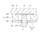
- FIG. 3 is an enlarged view of region III in FIG.
- the base body 13 has a space 21 for exposing the connection portion 16 to the outside of the base body 13 so that the connection portion 16 and the terminal 17 can be connected.
- the terminals 17 are arranged in the space 21.
- the terminal 17 is connected to the connecting portion 16 and is exposed to the outside of the base 13 from the lower surface 13 b of the base 13.
- the space 21 is in an empty state (vacuum state or state in which gas exists).
- the space 21 may be filled with a predetermined material (for example, a sealing material or a bonding material) in the manufacturing process of the heater 1. That is, after the heater 1 is completed, the space 21 need not be in an empty state as long as the material forming the base 13 is not located inside the space 21.
- a predetermined material for example, a sealing material or a bonding material
- the space 21 need not be in an empty state as long as the material forming the base 13 is not located inside the space 21.
- the portion of the base body 13 filled with the predetermined material is the space 21 is reasonably determined from the type of the material, the volume of the material, the shape of the portion filled with the material, the manufacturing process, and the like. May be done.
- the space 21 includes a first space 23 (see also FIG. 1) formed of a through hole penetrating the second insulating layer 19B and a second space 25 (see also FIG. 1) formed of a through hole penetrating the third insulating layer 19C. And have.
- the space 21 has a first space 23 that is in contact with the connection portion and a second space 25 that communicates the first space 23 with the outside of the lower surface 13b of the base 13.
- the shapes and dimensions of the first space 23 and the second space 25 may be set appropriately.
- the shape of the horizontal cross section of the first space 23 and/or the second space 25 parallel to the lower surface 13b of the base body 13 is an appropriate shape such as a circle (an example shown), an ellipse, a rectangle, or a polygon other than the rectangle. May be done.
- the shape of the vertical cross section orthogonal to the lower surface 13b of the base body 13 of the first space 23 and/or the second space 25 is a rectangle (an example shown), a trapezoidal shape whose diameter increases toward the lower surface 13b side, the lower surface 13b side. It may have a trapezoidal shape with a smaller diameter, or a shape that partially includes a curve (curved surface).
- one of the first space 23 and the second space 25 may be housed in the other, or both of them may coincide with each other.
- the second space 25 is smaller than the first space 23 and is accommodated in the first space 23 in the plan view of the lower surface 13b.
- a step 21a is formed at the boundary between the first space 23 and the second space 25.
- the second space 25 is open to a part of the surface of the first space 23 on the lower surface 13b side.
- the degree of difference between the two sizes may be set appropriately. For example, the difference in size between the two may be slightly larger than the processing error.
- the size (the thickness of the second insulating layer 19B and the third insulating layer 19C) of the first space 23 and the second space 25 in the direction (vertical direction) orthogonal to the lower surface 13b of the base 13 is larger than the other. May be.
- the vertical size of the second space 25 is smaller than the vertical size of the first space 23.
- the degree of the difference in size may be set appropriately.
- the size of the second space 25 in the vertical direction may be 1 ⁇ 2 or less or 1 ⁇ 3 or less of the size of the first space 23 in the vertical direction.
- the relative size of the space 21 with respect to the connecting portion 16 and the like may be appropriately set.
- the space 21 (each of the first space 23 and the second space 25) is provided for each connection part 16, for example. That is, the first space 23 contacts only one connecting portion 16 and does not overlap with two or more connecting portions 16. Further, the first space 23 may be accommodated in the connection portion 16 (in the illustrated example) or may coincide with the connection portion 16 in the plan view of the lower surface 13b of the base body 13, and may be larger than the connection portion 16. May extend to the outside.
- most of the space 21 is empty.
- the empty space 21 may be sealed or may not be sealed.
- the space 21 is sealed by providing a sealing material 29 interposed between the terminal 17 and the base 13.
- the closed space 21 may be filled with a gas or may be a vacuum.
- the enclosed gas may be, for example, an inert gas such as nitrogen.
- the vacuum is actually a state of being depressurized below atmospheric pressure. This can protect the connecting portion 16 and the like from oxidation.
- the space 21 is not closed, for example, the gas around the base 13 exists in the space 21.
- the material of the encapsulant 29 may be any appropriate material, and may be, for example, a material used for general glass encapsulation, or a CaO—Al 2 O 3 —Y 2 O 3 system or the like. Agents may be used.
- the sealing material 29 is filled in, for example, substantially the entire second space 25. However, the sealing material 29 may be arranged so that at least a part of the second space 25 is in an empty state. On the contrary, the sealing material 29 may be located in the first space 23 with a relatively large volume, or may be filled in the first space 23.
- the terminal 17 is arranged in the space 21, and one end thereof is joined to the connecting portion 16.
- the end of the terminal 17 opposite to the end connected to the connecting portion 16 may be located outside the lower surface 13b of the base 13 (illustrated example), or located in the second space 25. It may be located in the first space 23. At least a portion of the terminal 17 closer to the connecting portion 16 than the lower surface 13b is sized to pass through the second space 25.
- the terminal 17 may have a flange that faces (engages) the lower surface 13b around the second space 25.
- connection between the terminal 17 and the connecting portion 16 may be made by an appropriate method.
- the both are joined by a conductive joining material 27.
- the joining material 27 may be, for example, a brazing material such as an Ag—Cu—Ti alloy (an alloy containing Ag, Cu, and Ti).
- the bonding material 27 may be regarded as a part of the connecting portion 16, for example.
- the terminal 17 may only abut on the connecting portion 16.
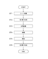
- FIG. 4 is a flowchart showing an example of the procedure of the method for manufacturing the heater plate 9.
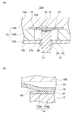
- 5(a), 5(b) and 6(a) are sectional views corresponding to FIG. 3, showing a part of the heater plate 9 in the process of being manufactured.
- the material and shape of each member change as the manufacturing process progresses. However, for convenience of explanation, the same reference numerals are used before and after a change in material, shape, and the like.
- step ST1 the first insulating layer 19A to the third insulating layer 19C (ceramic green sheet) before firing are prepared (see FIG. 5A).
- a through hole (first opening) to be the first space 23 is formed in the second insulating layer 19B (ceramic green sheet) before firing (see FIG. 5(a)).
- the method of forming the through holes may be the same as various known methods. For example, punching, cutting and/or laser processing may be used.
- the cutting tool used for cutting may be any appropriate tool, and for example, a drill may be used.
- a conductive paste to be the internal conductor 14 is arranged on the first insulating layer 19A to the third insulating layer 19C (ceramic green sheet) before firing (see FIG. 5A).
- a conductive paste that becomes the resistance heating element 15 including the connection portion 16 is arranged on the second insulating layer 19B side of the first insulating layer 19A.
- the order of steps ST2 and ST3 may be reversed.
- step ST4 the first insulating layer 19A to the third insulating layer 19C before firing are laminated to obtain the base body 13 (a laminated body of ceramic green sheets) before firing (see FIG. 5B). Since the second space 25 is not yet formed in the third insulating layer 19C, the first space 23 is closed and sealed by the third insulating layer 19C.
- the closed first space 23 may be evacuated or may be filled with gas.
- the gas may be, for example, an inert gas such as nitrogen.
- degreasing may be performed after the first insulating layer 19A to the third insulating layer 19C are laminated. Here, for example, if degreasing is performed in a nitrogen atmosphere, nitrogen is sealed in the sealed first space 23.
- the hermetically sealed first space 23 is filled with an inert gas such as nitrogen, the probability of oxidation of the connection portion 16 and the like is also increased during this period. Will be reduced.
- step ST5 the raw substrate 13 (a laminated body of ceramic green sheets) is fired.
- a through hole (second opening) to be the second space 25 is formed in the third insulating layer 19C of the base 13 after firing (FIG. 6(a)).
- the method of forming the through holes may be the same as various known methods. For example, cutting and/or laser processing may be used.
- FIG. 6A a mode in which cutting is performed by the cutting tool 31 (for example, a drill) is illustrated.
- the terminal 17 is inserted into the space 21 and joined to the connecting portion 16. Further, the sealing material 29 is arranged.
- the method of forming the through hole that becomes the second space 25 may be different from the method of forming the through hole that becomes the first space 23, or may be the same type.
- the former example there is a mode in which the first space 23 is formed by punching or laser processing, and the second space 25 is formed by cutting.
- An example of the latter is a mode in which both the first space 23 and the second space 25 are formed by cutting.
- the specific processing conditions may be different between the first space 23 and the second space 25, or may be the same. Specific working conditions include, for example, when a cutting tool is used, the shape and size of the cutting tool, the rotation speed of the cutting tool, and the feed speed of the cutting tool.
- the wall surface of the space 21 is the same as the first space 23.
- a difference in surface appearance between the second space 25 and the second space 25 can be observed.
- a cutting mark for example, a drill mark
- FIG. 6B is a perspective view schematically showing the wall surface of the second space 25 when the second space 25 is formed by the cutting tool 31, and schematically shows the cutting mark 33.
- the cutting traces 33 are observed as, for example, a striped pattern including a plurality of grooves 33a extending around the axis of the cutting tool (around the center line passing vertically through the second space 25).
- the ceramic structure (heater 1) has the base 13 and the internal conductor 14.
- the base 13 is made of ceramic and has a first surface (lower surface 13b).
- the inner conductor 14 is located in the base body 13 and has a connecting portion 16.
- the base body 13 has a space 21 extending from the connecting portion 16 to the lower surface 13b.
- the space 21 has a first space 23 and a second space 25.
- the first space 23 is in contact with the connecting portion 16.
- the second space 25 communicates with the first space 23 and the outside of the lower surface 13b, and is smaller than the first space 23 in plan view of the lower surface 13b.
- the area where the connecting portion 16 is exposed in the space 21 can be increased.
- the bonding area of the bonding material 27 for bonding the terminal 17 and the connecting portion 16 to the connecting portion 16 can be increased.
- the diameter of the second space 25 is small, the reliability of sealing the space 21 can be improved.
- the space 21 when the space 21 is evacuated or the space 21 is filled with a gas, the space 21 functions as a heat insulating portion.
- the heat of the resistance heating element 15 is hard to be transferred to the lower surface 13b, and is easily transferred to the upper surface 13a via the base 13. And the effect is improved because the first space 23 is relatively large in the plan view.
- the ceramic structure (heater 1) has a base 13 and an internal conductor 14.
- the base 13 is made of ceramic and has a first surface (lower surface 13b).
- the inner conductor 14 is located in the base body 13 and has a connecting portion 16.
- the base body 13 has a space 21 extending from the connecting portion 16 to the lower surface 13b.
- the wall surface of the space 21 has a first region (wall surface of the first space 23) and a second region (wall surface of the second space 25).
- the second region is located on the lower surface 13b side with respect to the first region, and has a surface appearance different from that of the first region.
- the difference in surface appearance can be used.
- the cutting mark 33 is formed on the inner wall of the second space 25
- the joint strength of the sealing material 29 to the wall surface of the second space 25 is improved due to the unevenness formed by the cutting mark 33.
- the cutting traces 33 are formed by a plurality of grooves 33 a that intersect the direction from the lower surface 13 b of the base body 13 to the connecting portion 16. Therefore, in the interface between the wall surface of the second space 25 and the sealing material 29, the path from the outside of the lower surface 13b of the base body 13 to the connecting portion 16 is longer than in the case where there is no cutting mark 33. As a result, the tightness of the space 21 is improved.
- the wall surface of the space 21 has a step 21 a at the boundary between the first space 23 and the second space 25.
- the strength of fixing the sealing material 29 to the base body 13 can be improved by engaging the sealing material 29 with the third insulating layer 19C from the first space 23 side.
- one space 21 has only one second space 25.
- the second space 25 it is easy to make the second space 25 as large as possible within the range of the size of the first space 23 or less. As a result, for example, it is easy to arrange the terminals 17 in the first space 23 via the second space 25.
- the method for manufacturing the ceramic structure includes a preparation step (step ST1), a conductor placement step (step ST3), a first opening forming step (step ST2), and a laminating step (step ST4). , A baking step (step ST5) and a second opening forming step (step ST6).
- the preparation step one or more first to third ceramic green sheets (first insulating layer 19A to third insulating layer 19C before firing) are prepared.
- the first ceramic green sheet constitutes a first portion (first insulating layer 19A) that is in contact with the inner conductor 14 of the base 13 on the side opposite to the first surface (lower surface 13b).
- the second ceramic green sheet constitutes a second portion (second insulating layer 19B) of the base 13 that is in contact with the inner conductor 14 on the lower surface 13b side.
- the third ceramic green sheet is in contact with the lower surface 13b side of the second insulating layer 19B of the base body 13 and constitutes a third portion (third insulating layer 19C) having the lower surface 13b.
- the conductor arranging step the material to be the inner conductor 14 is arranged on the lower surface 13b side of the first ceramic green sheet (first insulating layer 19A before firing).
- the first opening which is a part of the space 21 on the inner conductor 14 side (first space 23), is formed in the second ceramic green sheet (second insulating layer 19B before firing).
- the laminating step after the conductor arranging step and the first opening forming step, the first to third ceramic green sheets are laminated to obtain a laminated body (base 13 before firing).
- the laminated body is fired.
- the second opening forming step a part of the third portion (third insulating layer 19C) of the fired laminated body (base 13) overlapping the first space 23 on the lower surface 13b side of the space 21 (first A second opening is formed to be 2 spaces 25).
- the processing for forming the space 21 is performed only on the third insulating layer 19C, and the processing on the second insulating layer 19B is not necessary.
- the probability of damaging the connecting portion 16 by the process of forming the space 21 for the base body 13 after firing is reduced.
- the probability of cutting the connecting portion 16 with the cutting tool 31 is reduced.
- the connecting portion 16 is exposed to the atmosphere outside the base body 13 in the firing step and the like. As a result, for example, the connection part 16 may be oxidized and the characteristics of the connection part 16 may deteriorate.
- the probability of such oxidation is reduced. ..
- the tip side portion of the cutting tool 31 that has passed through the third insulating layer 19C is located in the first space 23. Therefore, it does not contact the base body 13.
- the impact applied from the cutting tool 31 to the portion of the base body 13 on the upper surface 13a side is reduced.
- the probability that a crack will occur on the upper surface 13a side of the base 13 can be reduced.
- the thickness of the base 13 from the internal conductor 14 to the upper surface 13a can be reduced.
- FIG. 7A is a sectional view showing a part of the heater plate 209 according to the first modification.
- This cross-sectional view generally corresponds to FIG. 3, but shows a cross section along the longitudinal direction of the resistance heating element 15 as shown by the resistance heating element 15 extending to the right side of the drawing.
- the features of the configuration shown in this figure may appear in the cross section in the same direction as in FIG.
- a plurality of second spaces 225 are provided for one first space 23.
- the size and arrangement of the plurality of second spaces 225 may be appropriately determined.
- the plurality of second spaces 225 may be arranged in one row, may be arranged two-dimensionally, or may be arranged in a mode that cannot be regarded as being arranged. ..
- the strength of the third insulating layer 19C immediately below the first space 23 it is easy to secure the strength of the third insulating layer 19C immediately below the first space 23.
- a plurality of second spaces 25 are arranged along the resistance heating element 15 as in the illustrated example, and the terminals 17 are inserted into the plurality of second spaces 25 to join the resistance heating elements 15. can do.
- the length of the first space 23 and/or the second space 25 in the width direction of the resistance heating element 15 is shortened to improve the strength of the base body 13 or the hermeticity of the space 221. can do.
- FIG. 7B is a sectional view corresponding to FIG. 3, showing a part of the heater plate 309 according to the second modification.
- the inner conductor 314 of the heater plate 309 includes a conductor layer (the resistance heating element 15 in the illustrated example) along the first surface (the lower surface 13b of the base 13) and a lower surface 13b with respect to the conductor layer. And the connecting conductor 35 that overlaps the side.
- the connecting conductor 35 constitutes a connecting portion 316 joined to the terminal 17. Note that only the connecting conductor may be regarded as the connecting portion 316, or a combination of a part of the resistance heating element 15 and the connecting conductor may be regarded as the connecting portion 316.
- the position, thickness, width, etc. of the connecting conductor 35 may be set appropriately.
- the connecting conductor 35 may be accommodated in the first space 23 (an example shown in the drawing), or may protrude from the first space 23 and be located between the first insulating layer 19A and the second insulating layer 19B. You may have a part.
- the connecting conductor 35 may cover the entire portion of the resistance heating element 15 that overlaps with the first space 23 in plan view (as shown in the drawing), or may cover a portion thereof.
- the thickness of the connecting conductor 35 may be thinner than, equal to, or thicker than the thickness of the resistance heating element 15 (example shown).
- the material of the connecting conductor 35 may be the same as or different from the material of the resistance heating element 15, or may be obtained by firing a conductive paste.
- the connecting conductor 35 may be provided by any suitable method at any suitable time as long as it is provided before the first insulating space 19C before firing closes the first space 23.
- the connecting conductor 35 may be arranged prior to stacking.
- the connecting portion 316 made of a shape and material more suitable for joining to the terminal 17 than the connecting portion 16 made of a part of the resistance heating element 15 can be realized.
- the second opening (second space 25) is formed in the third insulating layer 19C after firing by the cutting tool 31, the cutting tool 31 comes into contact with the connection portion 316. Even if it happens, the probability that the resistance heating element 15 (the main body of the inner conductor 314, the conductor layer) is cut is reduced.
- FIG. 8A is a cross-sectional view (cross-sectional view of the entire heater plate) corresponding to the line II-II in FIG. 1, showing the heater plate 409 according to the third modification.
- the space 421 has a layered space 37 in addition to the space 21 (space body) of the embodiment.
- the position, thickness and width of the layered space 37 may be set appropriately.
- the thickness of the layered space 37 is thinner than the thickness of the first space 23 and the second space 25.
- the specific thickness is, for example, 100 ⁇ m or less.
- the layered space 37 has, for example, the above-mentioned portion having a thickness of 100 ⁇ m or less over 50% or more, 80% or more, or all of the area of the layered space 37.
- the layered space 37 is formed, for example, between the first insulating layer 19A and the second insulating layer 19B. From another viewpoint, the layered space 37 is in contact with the internal conductor 14 (the same as the resistance heating element 15 in the illustrated example) from the first surface (lower surface 13b of the base 13) side. From still another viewpoint, the layered space 37 extends along the lower surface 13b from a part of the thickness of the space body (the space 21) in the direction (vertical direction) orthogonal to the lower surface 13b, which is in contact with the connecting portion 16. Is spreading.
- the layered space 37 is connected from one end to the other.
- the first insulating layer 19 ⁇ /b>A and the second insulating layer 19 ⁇ /b>B may be in contact with each other in a part of the arrangement region of the layered space 37, so that the layered space 37 may be divided in another vertical cross section.
- a part of the layered space 37 that does not communicate with the space 21 (the part may be regarded as a space different from the layered space 37 that communicates with the space 21) may occur. Good.
- the plurality of space bodies (spaces 21) are communicated with each other by the layered space 37, but such communication may not be performed.
- the layered space 37 may be expanded at an appropriate ratio with respect to the arrangement area of the internal conductor 14 (the same as the arrangement area of the resistance heating element 15 in the illustrated example). For example, assume the smallest circle or polygon (eg, rectangle) that accommodates the inner conductor 14 in plan perspective. At this time, the layered space 37 may extend over 10% or more, 30% or more, 50% or more, 80% or more, or all of the area of the circle or the polygon. In the above description, the area where the first insulating layer 19A and the second insulating layer 19B are in contact with each other in the arrangement area of the layered space 37 may be excluded from the area of the layered space 37, or may not be excluded. Good. Further, the layered space 37 may extend to the outside of the circle or the polygon.
- the method for forming the layered space 37 may be an appropriate method. For example, by appropriately setting the conditions for firing the laminated body of the ceramic green sheets, the gap between the first insulating layer 19A and the second insulating layer 19B can be utilized by utilizing the shrinkage accompanying the firing of the ceramic green sheets. May be generated to form the layered space 37. In addition, for example, by arranging a relatively small spacer between the first insulating layer 19A and the second insulating layer 19B when laminating the ceramic green sheets, the layered space 37 is formed before firing, or during firing. A gap due to contraction may be easily generated.
- the bonding material 27 in the molten state enters the layered space 37, and the bonding material 27 in the cured state becomes the first insulation of the second insulating layer 19B. Engages with the surface on the layer 19A side. This reduces the probability that the bonding material 27 will separate from the connecting portion 16. As a result, the reliability of the connection between the terminal 17 and the connecting portion 16 is improved.
- the volume of the space 421 or the layered space 37 is evacuated, or gas exists in 80% or more or all of the volume of the space 421 or the layered space 37 (for example, enclosed).
- the layered space 37 functions as a heat insulating layer.
- the heat escaping from the resistance heating element 15 to the lower surface 13b side of the base 13 can be reduced, and the heat can be easily transferred to the upper surface 13a of the base 13.
- the volume of the base 13 is secured, which is advantageous for securing the strength of the heater plate 409 and/or increasing the heat capacity.
- FIG. 8B is a sectional view similar to FIG. 8A, showing a heater plate 509 according to the fourth modification.
- the space 421 may extend over a relatively wide range (for example, 80% or more) of the arrangement region of the internal conductor 14 in the plan view of the first surface (the lower surface 13b of the base 13). It was Such an aspect may be realized by the first space 523, as shown in the fourth modification.
- the spacer 39 is provided between the first insulating layer 19A and the third insulating layer 19C.
- the spacer 39 contributes to ensuring the strength of the base 13, for example.
- the spacer 39 may be a part of the second insulating layer 19B or may be made of a material different from that of the second insulating layer 19B.
- the spacer 39 may have, for example, a column shape or a wall shape.
- the wall-shaped spacer 39 divides the space between the first insulating layer 19A and the third insulating layer 19C into a plurality of spaces and forms a space isolated from the first space 523 for exposing the connection portion 16. You may have. Of course, such a spacer 39 may not be provided.
- the fourth modified example is also an example in which one first space 523 is in contact with a plurality of connection parts 16 (overlapped in plan view).
- the second space 525 may also overlap the plurality of connecting portions 16 (an example shown in the drawing), or a plurality of second spaces. May individually overlap the plurality of connecting portions 16.
- FIG. 9A is a sectional view corresponding to FIG. 3, showing a heater plate 609 according to the fifth modification. Further, FIG. 9B is a schematic perspective view showing the appearance of the wall surface of the space 621 of the heater plate 609.
- the shape and size of the second space 625 are the same as the shape and size of the first space 23 when seen in a plan view.
- the wall surface of the space 621 does not have the step 21a (FIG. 3) and is continuous from the position of the connection portion 16 (the position of the upper surface of the second insulating layer 19B) to the lower surface 13b of the base 13.
- the heater plate 609 according to such a modified example is manufactured by, for example, the manufacturing method of the embodiment.
- the second opening (second space 625) is formed such that its shape and size are the same as the shape and size of the first opening (first space 23).
- the heater plate 609 may have the entire space 621 formed after firing. May have different characteristics.
- the internal conductor 14 (the lower surface of the first insulating layer 19A from another perspective) has a space 621 (first space 23), although it depends on the conditions of the stacking step and the firing step.
- the portion overlapping with is bent toward the first surface (the lower surface 13b of the base 13).
- the amount of bending is, for example, a size that can be visually recognized in an image obtained by capturing the cross section of the connecting portion 16.
- the difference between the highest position and the lowest position of the inner conductor 14 is 0.5 times or more, 1 time or more, 2 times or more of the thickness of the inner conductor 14, or It is more than 5 times.
- the shape of the bent portion of the inner conductor 14 may be any suitable shape. For example, it may be curved as a whole (example shown), or part or all may be formed linearly.
- FIG. 9B illustrates a mode in which the cutting mark 33 is formed only on the wall surface of the second space 625.
- the ceramic structure (heater plate 609) has the base 13 and the internal conductor 14.
- the base 13 is made of ceramic and has a first surface (lower surface 13b).
- the inner conductor 14 is located in the base body 13 and has a connecting portion 16.
- the base body 13 has a space 621 extending from the connection portion 16 to the lower surface 13b.
- the inner conductor 14 has a space 621 along the lower surface 13b and a conductor layer (for example, the resistance heating element 15) extending over the space 621. In the resistance heating element 15, a portion overlapping the space 621 is bent toward the lower surface 13b.
- connection part 16 is concave on the lower surface 13b side (such a mode may also be included in the technology according to the present disclosure)
- a space between the connection part 16 and the terminal 17 is provided. Therefore, the probability that the conductive area is reduced due to the formation of bubbles surrounded by the bonding material 27 is reduced.
- the volume of the base body 13 on the upper surface 13a side with respect to the internal conductor 14 can be increased to some extent to improve the heat storage property on the upper surface 13a side.
- connection portion 16 when a stress is generated between the terminal 17 (the bonding material 27 from another viewpoint) and the connection portion 16 due to the difference in thermal expansion between the base body 13 and the terminal 17, the stress is generated due to the elastic deformation of the connection portion 16. Expected to be alleviated.
- the wall surface of the space 621 is continuous from the position of the connection portion 16 to the first surface (the lower surface 13b of the base 13). From another viewpoint, the first space 23 and the second space 625 are coincident with each other in a plan view.
- the second space 625 is formed relatively large, it is easy to dispose the terminal 17 in the first space 23 and to join the terminal 17 and the connecting portion 16.
- FIG. 10A is a sectional view corresponding to FIG. 3, showing a heater plate 709 according to the sixth modification. Further, FIG. 10B is an enlarged view of the area Xb in FIG.
- the internal conductor 14 (more specifically, for example, the connecting portion 16) is bent toward the lower surface 13b side of the base 13 as in the fifth modification. Also, in the present modification, unlike the fifth modification, a gap 41 is formed between the internal conductor 14 and the base 13.
- the void 41 may be evacuated or gas may be present. The void 41 may or may not communicate with the space 21.
- the shape of the void 41 may be set appropriately.
- the void 41 is formed by the planar lower surface of the first insulating layer 19A and the upper surface of the inner conductor 14 that curves downward.
- the void 41 has a shape that is roughly formed by a plane and an arc in a cross-sectional view.
- both the lower surface of the first insulating layer 19A and the upper surface of the internal conductor 14 are curved downward, and the latter is largely deflected downward to form the void 41. May be.
- the lower surface of the void 41 (upper surface of the internal conductor 14) may include a flat portion.
- the shape of the void 41 in plan view is also arbitrary.
- the size of the void 41 may be set appropriately.
- the description of the amount of bending of the inner conductor 14 in the fifth modification may be applied to the inner conductor 14 in the present modification.
- the thickness of the void 41 (vertical direction) is a size that can be visually observed in an image obtained by imaging the cross section of the connection portion 16.
- the thickness of the void 41 may be set to 0.1 times or more, 0.5 times or more, 1 times or more, 2 times or more, or 5 times or more as large as the thickness of the connecting portion 16.
- the gap 41 may be wider than the upper end surface 17a of the terminal 17 (as shown in the figure), may be the same, or may be narrower.
- the void 41 may be formed by an appropriate method.
- the internal conductor 14 is separated from the lower surface of the first insulating layer 19A while leaving a space. 21 bends into. Thereby, the void 41 is formed.
- the resin may be arranged in a region of the lower surface of the first insulating layer 19A before firing, which is planned to overlap the first space 23, and the material to be the internal conductor 14 may be arranged thereon. In this case, the void 41 is formed by the disappearance of the resin in the firing process.
- the upper end surface 17a of the terminal 17 is joined to the connecting portion 16 only partially. That is, the upper end surface 17a has a joining region 17aa joined to the connecting portion 16 and a non-joining region 17ab not joined to the connecting portion 16.
- the non-bonding region 17ab faces, for example, the connecting portion 16 via the gap 43 (and the bonding material 27).
- the positions of the joining region 17aa and the non-joining region 17ab on the upper end surface 17a may be set appropriately.
- the non-bonding region 17ab (the gap 43 from another viewpoint) is set to extend from the bonding region 17aa to the outer edge of the upper end surface 17a. In this case, the gap 43 communicates with the space 21.
- the center of the upper end surface 17a is joined to the connecting portion 16 so as to face the convex top of the connecting portion 16 toward the lower surface 13b. Consequently, the joint region 17aa is a region on the center side of the upper end surface 17a, and the non-joint region 17ab is a region surrounding the joint region 17aa and/or a region located on both sides of the joint region 17aa in a predetermined cross section. Is becoming However, unlike the illustrated example, for example, a region eccentric from the center side of the upper end surface 17a may face the convex top of the connecting portion 16. Consequently, in a given cross section, the joining region 17aa may be located on one side in the lateral direction and the non-joining region 17ab may be located on the other side.
- the widths of the bonding area 17aa and the non-bonding area 17ab may be set appropriately.
- the former may be wider, equal, or narrower than the latter.
- the thickness of the gap 43 (vertical direction) may also be set appropriately.
- the thickness of the gap 43 (up and down direction) is a size that can be visually observed in an image of the cross section of the connection portion 16. Further, for example, the thickness of the gap 43 may be 0.1 times or more, 0.5 times or more, or 1 times or more the thickness of the connecting portion 16 at the maximum.
- the base body 13 and the connecting portion 16 are also included.
- An air gap 41 is located between and.
- the difference in thermal expansion between the terminal 17 and the base body 13 can be absorbed by the elastic deformation of the connecting portion 16.
- the thermal stress generated between the terminal 17 (the bonding material 27 from another viewpoint) and the connection portion 16 can be reduced, and the probability of peeling between the two can be reduced.
- the thermal stress generated between the terminal 17 and the base body 13 can be reduced, and the probability that a crack will occur in the base body 13 can be reduced.
- the upper end surface 17 a of the terminal 17 reaches the joining region 17 aa joined to the connecting portion 16 and reaches the outer edge of the upper end face 17 a from the joining region 17 aa and faces the connecting portion 16 via the gap 43. And a non-bonding region 17ab that is being formed.
- each of the heater 1, the heater plates 9, 209, 309, 409, 509, 609 and 709 is an example of a ceramic structure.
- the lower surface 13b of the base 13 is an example of the first surface.
- the resistance heating element 15 is an example of a conductor layer.
- the wall surfaces of the first spaces 23 and 523 are examples of the first region.
- the wall surfaces of the second spaces 25, 225, 525, and 625 are examples of the second region.
- the spaces 21, 221 and 621 are examples of space bodies.
- the first insulating layer 19A is an example of the first portion.
- the second insulating layer 19B is an example of the second portion.
- the third insulating layer 19C is an example of the third portion.
- the first insulating layer 19A before firing is an example of a first ceramic green sheet.
- the second insulating layer 19B before firing is an example of a second ceramic green sheet.
- the third insulating layer 19C before firing is an example of a third ceramic green sheet.
- Each of the first spaces 23 and 523 is an example of the first opening.
- Each of the second spaces 25, 225, 525 and 625 is an example of the second opening.
- the heater according to the present disclosure is not limited to the above embodiments and modifications, and may be implemented in various modes.
- the connecting conductor 35 of FIG. 7B may be combined with various modified examples.
- the layered space 37 of FIG. 8A may be combined with a configuration in which the first space 23 and the second space 625 are coincident with each other in plan view as shown in FIG. 9A.
- a heater plate having a heating function is taken as an example of the ceramic structure.
- the ceramic structure may have other functions.
- the ceramic structure may be an electrostatic chuck or an electrode member for plasma generation, or may function as a combination of two or more of these and a heater.
- the ceramic structure is not limited to such a wafer processing object (such as a susceptor) but can be applied to any technical field.
- the inner conductor was a resistance heating element for heating in the embodiment, but may be a conductor for other applications, such as an electrode for an electrostatic chuck or an electrode for plasma generation. May be.
- the ceramic structure may have one or a combination of two or more of these electrodes and resistance heating elements.
- the inner conductor may be, for example, a conductor having a shape that can be said to spread (face upward) along the upper surface of the base body (13) as a whole. Further, for example, when the minimum convex curve that surrounds the entire inner conductor is assumed in plan view, the region surrounded by the convex curve may occupy 60% or more or 80% or more of the upper surface of the base.
- the internal conductors need not be conductors directly responsible for the function of the ceramic structure, such as a resistance heating element or an electrode.
- a wiring layer for connecting the resistance heating element and/or the electrode to the terminal may be provided between the resistance heating element and/or the electrode and the lower surface of the base.
- the connection portion that is in contact with the space may be configured by a part of the wiring layer or the connection conductor that is overlapped on the part. That is, the inner conductor may include a wiring layer.
- the base body is located on the opposite side of the first space from the first space (the embodiment. Then, there is an effect that the impact applied to the upper surface 13a side) can be relaxed.
- the electrostatic chuck has a relatively small thickness (for example, 0.3 ⁇ m or less) from the electrode (internal conductor) in the base to the upper surface of the base. Therefore, when the technique according to the present disclosure is applied to the electrostatic chuck as the ceramic structure, the above effects are effectively exhibited. The same applies when the technique according to the present disclosure is applied to a focus ring with a built-in electrode as a ceramic structure that is used for generating plasma or the like. Further, a heat exchanger as a ceramic structure, which includes a heater and heats a fluid or a chemical composition, may have thin fins. Even when the technique according to the present disclosure is applied to such a ceramic structure, the above effects are effectively exhibited.
- SYMBOLS 1... Heater (ceramic structure), 13... Base
Landscapes
- Engineering & Computer Science (AREA)
- Ceramic Engineering (AREA)
- Chemical & Material Sciences (AREA)
- Mechanical Engineering (AREA)
- Manufacturing & Machinery (AREA)
- Structural Engineering (AREA)
- Resistance Heating (AREA)
- Devices For Post-Treatments, Processing, Supply, Discharge, And Other Processes (AREA)
- Container, Conveyance, Adherence, Positioning, Of Wafer (AREA)
Abstract
Description
図1は、実施形態に係るヒータ1の構成を示す模式的な分解斜視図である。図2は、図1のヒータ1を含むヒータシステム101の構成を示す模式図である。図2において、ヒータ1については、図1のII-II線断面図が示されている。図1は、ヒータ1の構造を示すために便宜的にヒータ1を分解して示しており、実際の完成後のヒータ1は、図1の分解斜視図のように分解可能である必要はない。
ヒータ1は、例えば、概略板状(図示の例では円盤状)のヒータプレート9と、ヒータプレート9から下方へ延びているパイプ11とを有している。
ヒータプレート9の上面13a及び下面13bは、例えば、概ね平面である。ヒータプレート9の平面形状及び各種の寸法は、加熱対象物の形状及び寸法等を考慮して適宜に設定されてよい。例えば、平面形状は、円形(図示の例)又は多角形(例えば矩形)である。寸法の一例を示すと、直径は20cm以上35cm以下、厚さは4mm以上30mm以下である。なお、本実施形態の説明において、矩形等の多角形に係る用語は、特に断りが無い限り、角部が直線(平面)又は曲線(曲面)によって面取りされた形状を含んでよいものとする。
基体13の外形は、ヒータプレート9の外形を構成している。従って、上述のヒータプレート9の形状及び寸法に係る説明は、そのまま基体13の外形及び寸法の説明と捉えられてよい。基体13の材料は、例えば、セラミックである。セラミックは、例えば、窒化アルミニウム(AlN)、酸化アルミニウム(Al2O3、アルミナ)、炭化珪素(SiC)、及び窒化珪素(Si3N4)等を主成分とする焼結体である。なお、主成分は、例えば、その材料の50質量%以上又は80質量%以上を占める材料である(以下、特に断りが無い限り、他の部材及び他の材料についても、同様である。)。
抵抗発熱体15は、基体13の上面13a及び下面13bに沿って(例えば平行に)延びている。また、抵抗発熱体15は、平面視において、例えば、基体13の概ね全面に亘って延びている。
接続部16は、抵抗発熱体15の一部によって構成されていてもよいし、抵抗発熱体15とは別個の部位として構成され、抵抗発熱体15と端子17との間に介在していてもよい。また、別の観点では、接続部16の材料、幅及び/又は厚さは、抵抗発熱体15の材料、幅及び/又は厚さと同一であってもよいし、異なっていてもよい。
端子17は、例えば、接続部16の数と同数で設けられ、接続部16に接合されているとともに、一部が基体13の下面13bから基体13の外部へ露出している。これにより、ヒータプレート9の外部から端子17及び接続部16を介して抵抗発熱体15へ電力を供給可能になっている。端子17は、例えば、少なくとも表面に導電性を有する部材によって構成されている。例えば、端子17は、その全体が金属からなるバルク材(金属部材)によって構成されている。端子17の形状は適宜なものとされてよく、例えば、概略、柱状(軸状)である。その軸に直交する横断面の形状は、円形等の適宜な形状とされてよい。端子17の軸方向(上下方向)の長さと径とはいずれが大きくてもよい。
パイプ11は、上下(軸方向両側)が開口している中空状である。別の観点では、パイプ11は、上下に貫通する空間11sを有している。パイプ11の横断面(軸方向に直交する断面)及び縦断面(軸方向に平行な断面。図2に示す断面)の形状は適宜に設定されてよい。図示の例では、パイプ11は、軸方向の位置に対して径が一定の円筒形状である。もちろん、パイプ11は、高さ方向の位置によって径が異なっていてもよい。また、パイプ11の寸法の具体的な値は適宜に設定されてよい。特に図示しないが、パイプ11には、気体又は液体が流れる流路が形成されていてもよい。
配線部材7は、パイプ11の空間11s内に挿通されている。平面透視において、ヒータプレート9のうち空間11s内に露出する領域では、複数の端子17が基体13から露出している。そして、配線部材7は、その一端が複数の端子17に接続されている。
図3は、図2の領域IIIの拡大図である。
図4は、ヒータプレート9の製造方法の手順の一例を示すフローチャートである。また、図5(a)、図5(b)及び図6(a)は、製造途中のヒータプレート9の一部を示す、図3に相当する断面図である。各部材の材質及び形状等は、製造過程の進行に伴って変化する。ただし、説明の便宜上、材質及び形状等の変化の前後で同一の符号を用いる。
以下では、種々の変形例について述べる。変形例の説明では、基本的に、実施形態との相違点について述べる。特に言及しない点については、例えば、実施形態と同様とされたり、実施形態から類推されたりしてよい。また、変形例において、実施形態の構成と対応又は類似する構成については、相違点があっても、便宜上、同一の符号を付すことがある。また、以下の説明では、端子17、接合材27及び封止材29の図示を省略することがある。
図7(a)は、第1変形例に係るヒータプレート209の一部を示す断面図である。この断面図は、図3に概ね対応しているが、抵抗発熱体15が紙面右側に延びていることによって示されているように、抵抗発熱体15の長手方向に沿う断面を示している。ただし、図3と同一の方向の断面において、この図に示す構成の特徴が現れていてもよい。
図7(b)は、第2変形例に係るヒータプレート309の一部を示す、図3に対応する断面図である。
図8(a)は、第3変形例に係るヒータプレート409を示す、図1のII-II線に対応する断面図(ヒータプレートの全体の断面図)である。
図8(b)は、第4変形例に係るヒータプレート509を示す、図8(a)と同様の断面図である。
図9(a)は、第5変形例に係るヒータプレート609を示す、図3に相当する断面図である。また、図9(b)は、ヒータプレート609の空間621の壁面の様相を示す模式的な斜視図である。
図10(a)は、第6変形例に係るヒータプレート709を示す、図3に相当する断面図である。また、図10(b)は、図10(a)の領域Xbの拡大図である。
Claims (15)
- セラミックからなり、第1面を有している基体と、
前記基体内に位置しており、接続部を有している内部導体と、
を有しており、
前記基体は、前記接続部から前記第1面に亘っている空間を有しており、
前記空間は、
前記接続部に接している第1空間と、
前記第1空間と前記第1面の外側とを連通しており、前記第1面の平面透視において前記第1空間よりも小さい第2空間と、を有している
セラミック構造体。 - セラミックからなり、第1面を有している基体と、
前記基体内に位置しており、接続部を有している内部導体と、
を有しており、
前記基体は、前記接続部から前記第1面に亘っている空間を有しており、
前記内部導体は、前記第1面に沿って前記空間及びその外側に跨っている導体層を有しており、
前記導体層は、前記空間に重なる部分が前記第1面側に撓んでいる
セラミック構造体。 - セラミックからなり、第1面を有している基体と、
前記基体内に位置しており、接続部を有している内部導体と、
を有しており、
前記基体は、前記接続部から前記第1面に亘っている空間を有しており、
前記空間の壁面は、
第1領域と、
前記第1領域に対して前記第1面側に位置しており、前記第1領域とは表面の様相が異なる第2領域とを有している
セラミック構造体。 - 前記空間の壁面は、前記第1空間と前記第2空間との境界に段差を有している
請求項1に記載のセラミック構造体。 - 前記空間は、1つのみ前記第2空間を有している
請求項1又は4に記載のセラミック構造体。 - 前記空間は、複数の前記第2空間を有している
請求項1又は4に記載のセラミック構造体。 - 前記基体と前記接続部との間に空隙が位置している
請求項2に記載のセラミック構造体。 - 上端面が前記接続部に接合されている端子を更に有しており、
前記上端面は、
前記接続部に接合されている接合領域と、
前記接合領域から前記上端面の外縁に至り、前記接続部と隙間を介して対向している非接合領域と、を有している
請求項2又は7に記載のセラミック構造体。 - 前記空間の壁面は、前記接続部の位置から前記第1面まで連続している
請求項2、3、7又は8に記載のセラミック構造体。 - 前記第1領域及び前記第2領域のうち前記第2領域のみが切削痕を有している
請求項3に記載のセラミック構造体。 - 前記空間の容積の少なくとも8割以上は真空とされ、又は前記空間の容積の少なくとも8割以上には気体が存在している
請求項1~10のいずれか1項に記載のセラミック構造体。 - 前記空間は、
前記接続部から前記第1面に亘っている空間本体と、
前記空間本体の、前記第1面に直交する方向の厚みのうち、前記接続部に接している一部の厚みから前記第1面に沿って広tがっている、100μm以下の層状空間と、を有している
請求項11に記載のセラミック構造体。 - 前記空間は、前記第1面の平面透視において前記内部導体の配置領域の8割以上に亘っている
請求項11又は12に記載のセラミック構造体。 - 前記内部導体は、
前記第1面に沿っている導体層と、
前記導体層のうち一部のみに対して前記第1面側に重なっており、前記接続部を構成している接続用導体と、を有している
請求項1~13のいずれか1項に記載のセラミック構造体。 - 請求項1~14のセラミック構造体の製造方法であって、
前記基体のうち前記内部導体に対して前記第1面とは反対側に接する第1部分を構成する1以上の第1セラミックグリーンシートと、前記基体のうち前記内部導体に対して前記第1面側に接する第2部分を構成する1以上の第2セラミックグリーンシートと、前記基体のうち前記第2部分の前記第1面側に接するとともに前記第1面を有している第3部分を構成する1以上の第3セラミックグリーンシートと、を準備する準備工程と、
前記内部導体となる材料を前記第1セラミックグリーンシートの前記第1面側に配置する導体配置工程と、
前記空間のうち前記内部導体側の一部となる第1開口を前記第2セラミックグリーンシートに形成する第1開口形成工程と、
前記導体配置工程及び前記第1開口形成工程の後に、前記第1~第3セラミックグリーンシートを積層して積層体を得る積層工程と、
前記積層体を焼成する焼成工程と、
焼成後の前記積層体における前記第3部分のうち前記第1開口に重なっている領域に前記空間の前記第1面側の一部となる第2開口を形成する第2開口形成工程と、
を有しているセラミック構造体の製造方法。
Priority Applications (2)
| Application Number | Priority Date | Filing Date | Title |
|---|---|---|---|
| JP2020557582A JP7195336B2 (ja) | 2018-11-30 | 2019-11-20 | セラミック構造体及びセラミック構造体の製造方法 |
| US17/292,246 US12550231B2 (en) | 2018-11-30 | 2019-11-20 | Ceramic structure and method manufacturing ceramic structure |
Applications Claiming Priority (2)
| Application Number | Priority Date | Filing Date | Title |
|---|---|---|---|
| JP2018224680 | 2018-11-30 | ||
| JP2018-224680 | 2018-11-30 |
Publications (1)
| Publication Number | Publication Date |
|---|---|
| WO2020110850A1 true WO2020110850A1 (ja) | 2020-06-04 |
Family
ID=70853156
Family Applications (1)
| Application Number | Title | Priority Date | Filing Date |
|---|---|---|---|
| PCT/JP2019/045380 Ceased WO2020110850A1 (ja) | 2018-11-30 | 2019-11-20 | セラミック構造体及びセラミック構造体の製造方法 |
Country Status (3)
| Country | Link |
|---|---|
| US (1) | US12550231B2 (ja) |
| JP (1) | JP7195336B2 (ja) |
| WO (1) | WO2020110850A1 (ja) |
Citations (5)
| Publication number | Priority date | Publication date | Assignee | Title |
|---|---|---|---|---|
| JP2003179127A (ja) * | 2001-12-11 | 2003-06-27 | Taiheiyo Cement Corp | 静電チャック用給電端子 |
| JP2008305968A (ja) * | 2007-06-07 | 2008-12-18 | Sei Hybrid Kk | ウェハ保持体の電極接続構造 |
| JP2013084938A (ja) * | 2011-09-30 | 2013-05-09 | Toto Ltd | 静電チャック |
| JP2017153254A (ja) * | 2016-02-25 | 2017-08-31 | 京セラ株式会社 | 半導体製造装置用部品 |
| JP2018016536A (ja) * | 2016-07-29 | 2018-02-01 | 日本特殊陶業株式会社 | セラミックス部材 |
Family Cites Families (6)
| Publication number | Priority date | Publication date | Assignee | Title |
|---|---|---|---|---|
| US7714235B1 (en) * | 1997-05-06 | 2010-05-11 | Formfactor, Inc. | Lithographically defined microelectronic contact structures |
| JP4548928B2 (ja) | 2000-10-31 | 2010-09-22 | 京セラ株式会社 | 電極内蔵体及びこれを用いたウエハ支持部材 |
| JP2003040686A (ja) | 2001-07-27 | 2003-02-13 | Taiheiyo Cement Corp | セラミック部品 |
| JP4089820B2 (ja) * | 2003-04-02 | 2008-05-28 | 日本発条株式会社 | 静電チャック |
| JP5591627B2 (ja) | 2010-08-24 | 2014-09-17 | 太平洋セメント株式会社 | セラミックス部材及びその製造方法 |
| JP2019060819A (ja) * | 2017-09-28 | 2019-04-18 | 日本特殊陶業株式会社 | 電子部品検査装置用配線基板 |
-
2019
- 2019-11-20 JP JP2020557582A patent/JP7195336B2/ja active Active
- 2019-11-20 WO PCT/JP2019/045380 patent/WO2020110850A1/ja not_active Ceased
- 2019-11-20 US US17/292,246 patent/US12550231B2/en active Active
Patent Citations (5)
| Publication number | Priority date | Publication date | Assignee | Title |
|---|---|---|---|---|
| JP2003179127A (ja) * | 2001-12-11 | 2003-06-27 | Taiheiyo Cement Corp | 静電チャック用給電端子 |
| JP2008305968A (ja) * | 2007-06-07 | 2008-12-18 | Sei Hybrid Kk | ウェハ保持体の電極接続構造 |
| JP2013084938A (ja) * | 2011-09-30 | 2013-05-09 | Toto Ltd | 静電チャック |
| JP2017153254A (ja) * | 2016-02-25 | 2017-08-31 | 京セラ株式会社 | 半導体製造装置用部品 |
| JP2018016536A (ja) * | 2016-07-29 | 2018-02-01 | 日本特殊陶業株式会社 | セラミックス部材 |
Also Published As
| Publication number | Publication date |
|---|---|
| JP7195336B2 (ja) | 2022-12-23 |
| JPWO2020110850A1 (ja) | 2021-10-14 |
| US20220007466A1 (en) | 2022-01-06 |
| US12550231B2 (en) | 2026-02-10 |
Similar Documents
| Publication | Publication Date | Title |
|---|---|---|
| US12525472B2 (en) | Structure and heating device | |
| US12238827B2 (en) | Base structure and wafer placing device | |
| JP7448060B1 (ja) | 静電チャック | |
| JP7175323B2 (ja) | セラミック構造体及びウェハ用システム | |
| US11856659B2 (en) | Board-like structure and heater system | |
| JP7195336B2 (ja) | セラミック構造体及びセラミック構造体の製造方法 | |
| JP7321285B2 (ja) | セラミック構造体及びウェハ用システム | |
| WO2020110954A1 (ja) | セラミック構造体及び端子付構造体 | |
| JP7175324B2 (ja) | セラミック構造体及びウェハ用システム | |
| US12183601B2 (en) | Structural body and heating apparatus | |
| JP2020107519A (ja) | 多層基板及びその製造方法 | |
| JP7360992B2 (ja) | 端子付構造体 | |
| US20210400800A1 (en) | Board-like structure and heater system | |
| JP7145226B2 (ja) | ウェハ用部材、ウェハ用システム及びウェハ用部材の製造方法 | |
| JP7169793B2 (ja) | 保持装置 | |
| JP7037477B2 (ja) | 多層基板及びその製造方法 | |
| WO2025154186A1 (ja) | セラミックサセプタ及びその製造方法 | |
| JP2023088272A (ja) | 基板保持部材及び基板保持部材の製造方法 | |
| WO2021065544A1 (ja) | 構造体および加熱装置 | |
| JP2003249329A (ja) | 面状セラミックスヒーター及び製造方法 |
Legal Events
| Date | Code | Title | Description |
|---|---|---|---|
| 121 | Ep: the epo has been informed by wipo that ep was designated in this application |
Ref document number: 19890028 Country of ref document: EP Kind code of ref document: A1 |
|
| ENP | Entry into the national phase |
Ref document number: 2020557582 Country of ref document: JP Kind code of ref document: A |
|
| NENP | Non-entry into the national phase |
Ref country code: DE |
|
| 122 | Ep: pct application non-entry in european phase |
Ref document number: 19890028 Country of ref document: EP Kind code of ref document: A1 |
|
| WWG | Wipo information: grant in national office |
Ref document number: 17292246 Country of ref document: US |