WO2020105634A1 - 固体撮像装置および電子機器 - Google Patents
固体撮像装置および電子機器Info
- Publication number
- WO2020105634A1 WO2020105634A1 PCT/JP2019/045276 JP2019045276W WO2020105634A1 WO 2020105634 A1 WO2020105634 A1 WO 2020105634A1 JP 2019045276 W JP2019045276 W JP 2019045276W WO 2020105634 A1 WO2020105634 A1 WO 2020105634A1
- Authority
- WO
- WIPO (PCT)
- Prior art keywords
- imaging device
- solid
- state imaging
- insulating film
- photoelectric conversion
- Prior art date
- Legal status (The legal status is an assumption and is not a legal conclusion. Google has not performed a legal analysis and makes no representation as to the accuracy of the status listed.)
- Ceased
Links
Images


Classifications
-
- H—ELECTRICITY
- H10—SEMICONDUCTOR DEVICES; ELECTRIC SOLID-STATE DEVICES NOT OTHERWISE PROVIDED FOR
- H10F—INORGANIC SEMICONDUCTOR DEVICES SENSITIVE TO INFRARED RADIATION, LIGHT, ELECTROMAGNETIC RADIATION OF SHORTER WAVELENGTH OR CORPUSCULAR RADIATION
- H10F39/00—Integrated devices, or assemblies of multiple devices, comprising at least one element covered by group H10F30/00, e.g. radiation detectors comprising photodiode arrays
- H10F39/80—Constructional details of image sensors
- H10F39/803—Pixels having integrated switching, control, storage or amplification elements
- H10F39/8037—Pixels having integrated switching, control, storage or amplification elements the integrated elements comprising a transistor
-
- H—ELECTRICITY
- H10—SEMICONDUCTOR DEVICES; ELECTRIC SOLID-STATE DEVICES NOT OTHERWISE PROVIDED FOR
- H10F—INORGANIC SEMICONDUCTOR DEVICES SENSITIVE TO INFRARED RADIATION, LIGHT, ELECTROMAGNETIC RADIATION OF SHORTER WAVELENGTH OR CORPUSCULAR RADIATION
- H10F39/00—Integrated devices, or assemblies of multiple devices, comprising at least one element covered by group H10F30/00, e.g. radiation detectors comprising photodiode arrays
- H10F39/80—Constructional details of image sensors
- H10F39/802—Geometry or disposition of elements in pixels, e.g. address-lines or gate electrodes
- H10F39/8023—Disposition of the elements in pixels, e.g. smaller elements in the centre of the imager compared to larger elements at the periphery
-
- H—ELECTRICITY
- H10—SEMICONDUCTOR DEVICES; ELECTRIC SOLID-STATE DEVICES NOT OTHERWISE PROVIDED FOR
- H10F—INORGANIC SEMICONDUCTOR DEVICES SENSITIVE TO INFRARED RADIATION, LIGHT, ELECTROMAGNETIC RADIATION OF SHORTER WAVELENGTH OR CORPUSCULAR RADIATION
- H10F39/00—Integrated devices, or assemblies of multiple devices, comprising at least one element covered by group H10F30/00, e.g. radiation detectors comprising photodiode arrays
- H10F39/80—Constructional details of image sensors
- H10F39/803—Pixels having integrated switching, control, storage or amplification elements
-
- H—ELECTRICITY
- H04—ELECTRIC COMMUNICATION TECHNIQUE
- H04N—PICTORIAL COMMUNICATION, e.g. TELEVISION
- H04N25/00—Circuitry of solid-state image sensors [SSIS]; Control thereof
- H04N25/70—SSIS architectures; Circuits associated therewith
- H04N25/76—Addressed sensors, e.g. MOS or CMOS sensors
- H04N25/77—Pixel circuitry, e.g. memories, A/D converters, pixel amplifiers, shared circuits or shared components
-
- H—ELECTRICITY
- H10—SEMICONDUCTOR DEVICES; ELECTRIC SOLID-STATE DEVICES NOT OTHERWISE PROVIDED FOR
- H10F—INORGANIC SEMICONDUCTOR DEVICES SENSITIVE TO INFRARED RADIATION, LIGHT, ELECTROMAGNETIC RADIATION OF SHORTER WAVELENGTH OR CORPUSCULAR RADIATION
- H10F39/00—Integrated devices, or assemblies of multiple devices, comprising at least one element covered by group H10F30/00, e.g. radiation detectors comprising photodiode arrays
- H10F39/10—Integrated devices
- H10F39/12—Image sensors
- H10F39/18—Complementary metal-oxide-semiconductor [CMOS] image sensors; Photodiode array image sensors
-
- H—ELECTRICITY
- H10—SEMICONDUCTOR DEVICES; ELECTRIC SOLID-STATE DEVICES NOT OTHERWISE PROVIDED FOR
- H10F—INORGANIC SEMICONDUCTOR DEVICES SENSITIVE TO INFRARED RADIATION, LIGHT, ELECTROMAGNETIC RADIATION OF SHORTER WAVELENGTH OR CORPUSCULAR RADIATION
- H10F39/00—Integrated devices, or assemblies of multiple devices, comprising at least one element covered by group H10F30/00, e.g. radiation detectors comprising photodiode arrays
- H10F39/80—Constructional details of image sensors
- H10F39/802—Geometry or disposition of elements in pixels, e.g. address-lines or gate electrodes
-
- H—ELECTRICITY
- H10—SEMICONDUCTOR DEVICES; ELECTRIC SOLID-STATE DEVICES NOT OTHERWISE PROVIDED FOR
- H10F—INORGANIC SEMICONDUCTOR DEVICES SENSITIVE TO INFRARED RADIATION, LIGHT, ELECTROMAGNETIC RADIATION OF SHORTER WAVELENGTH OR CORPUSCULAR RADIATION
- H10F39/00—Integrated devices, or assemblies of multiple devices, comprising at least one element covered by group H10F30/00, e.g. radiation detectors comprising photodiode arrays
- H10F39/80—Constructional details of image sensors
- H10F39/807—Pixel isolation structures
-
- H—ELECTRICITY
- H10—SEMICONDUCTOR DEVICES; ELECTRIC SOLID-STATE DEVICES NOT OTHERWISE PROVIDED FOR
- H10F—INORGANIC SEMICONDUCTOR DEVICES SENSITIVE TO INFRARED RADIATION, LIGHT, ELECTROMAGNETIC RADIATION OF SHORTER WAVELENGTH OR CORPUSCULAR RADIATION
- H10F39/00—Integrated devices, or assemblies of multiple devices, comprising at least one element covered by group H10F30/00, e.g. radiation detectors comprising photodiode arrays
- H10F39/80—Constructional details of image sensors
- H10F39/811—Interconnections
-
- H—ELECTRICITY
- H10—SEMICONDUCTOR DEVICES; ELECTRIC SOLID-STATE DEVICES NOT OTHERWISE PROVIDED FOR
- H10F—INORGANIC SEMICONDUCTOR DEVICES SENSITIVE TO INFRARED RADIATION, LIGHT, ELECTROMAGNETIC RADIATION OF SHORTER WAVELENGTH OR CORPUSCULAR RADIATION
- H10F39/00—Integrated devices, or assemblies of multiple devices, comprising at least one element covered by group H10F30/00, e.g. radiation detectors comprising photodiode arrays
- H10F39/011—Manufacture or treatment of image sensors covered by group H10F39/12
- H10F39/014—Manufacture or treatment of image sensors covered by group H10F39/12 of CMOS image sensors
-
- H—ELECTRICITY
- H10—SEMICONDUCTOR DEVICES; ELECTRIC SOLID-STATE DEVICES NOT OTHERWISE PROVIDED FOR
- H10F—INORGANIC SEMICONDUCTOR DEVICES SENSITIVE TO INFRARED RADIATION, LIGHT, ELECTROMAGNETIC RADIATION OF SHORTER WAVELENGTH OR CORPUSCULAR RADIATION
- H10F39/00—Integrated devices, or assemblies of multiple devices, comprising at least one element covered by group H10F30/00, e.g. radiation detectors comprising photodiode arrays
- H10F39/80—Constructional details of image sensors
- H10F39/805—Coatings
- H10F39/8053—Colour filters
-
- H—ELECTRICITY
- H10—SEMICONDUCTOR DEVICES; ELECTRIC SOLID-STATE DEVICES NOT OTHERWISE PROVIDED FOR
- H10F—INORGANIC SEMICONDUCTOR DEVICES SENSITIVE TO INFRARED RADIATION, LIGHT, ELECTROMAGNETIC RADIATION OF SHORTER WAVELENGTH OR CORPUSCULAR RADIATION
- H10F39/00—Integrated devices, or assemblies of multiple devices, comprising at least one element covered by group H10F30/00, e.g. radiation detectors comprising photodiode arrays
- H10F39/80—Constructional details of image sensors
- H10F39/805—Coatings
- H10F39/8057—Optical shielding
Definitions
- the present disclosure relates to a solid-state imaging device that performs imaging by performing photoelectric conversion, and an electronic device including the solid-state imaging device.
- a solid-state imaging device includes a semiconductor layer, a photoelectric conversion unit that is provided in the semiconductor layer and generates a charge according to the amount of received light by photoelectric conversion, and a first electrical element provided in the semiconductor layer.
- a storage capacitor element including a first insulating film having a film thickness, and a first insulating film provided in the semiconductor layer and having a second electric film thickness larger than the first electric film thickness.
- a transistor a transistor.
- the insulating film of the storage capacitor can be thinned by the above configuration, so that the capacitance of the storage capacitor can be increased without expanding the area occupied by the storage capacitor. To do.
- FIG. 3 is a block diagram showing a configuration example of functions of the solid-state imaging device according to the first embodiment of the present disclosure. It is a block diagram which shows the structural example of a function of the solid-state imaging device as a 1st modification. It is a block diagram which shows the structural example of the function of the solid-state imaging device as a 2nd modification.
- FIG. 1B is a circuit diagram showing a circuit configuration example of one sensor pixel in the solid-state imaging device shown in FIG. 1A.
- FIG. 3 is a plan view illustrating a planar configuration example of the sensor pixel illustrated in FIG. 2.
- FIG. 3 is a cross-sectional view showing a cross-sectional configuration example of the sensor pixel shown in FIG. 2.
- FIG. 1B is a circuit diagram showing a circuit configuration example of one sensor pixel in the solid-state imaging device shown in FIG. 1A.
- FIG. 3 is a plan view illustrating a planar configuration example of the sensor pixel illustrated in FIG. 2.
- FIG. 9 is a cross-sectional view showing a step in the method of manufacturing the sensor pixel shown in FIG. 2. It is sectional drawing showing 1 process following FIG. 5A. It is sectional drawing showing 1 process following FIG. 5B.
- FIG. 5C is a cross-sectional view showing a process following FIG. 5C. It is sectional drawing showing 1 process following FIG. 5D.
- FIG. 5C is a cross-sectional view showing a process following FIG. 5E. It is sectional drawing showing 1 process of following FIG. 5F.
- FIG. 16 is a circuit diagram illustrating a circuit configuration example of one sensor pixel in the solid-state imaging device according to the second embodiment of the present disclosure.
- FIG. 16 is a circuit diagram illustrating a circuit configuration example of one sensor pixel in the solid-state imaging device according to the second embodiment of the present disclosure.
- FIG. 7 is an explanatory diagram including a partial cross-sectional configuration example of the sensor pixel shown in FIG. 6.
- FIG. 16 is a circuit diagram illustrating a circuit configuration example of one sensor pixel in the solid-state imaging device according to the third embodiment of the present disclosure.
- FIG. 9 is an explanatory diagram including a partial cross-sectional configuration example of the sensor pixel shown in FIG. 8.
- FIG. 16 is a plan view illustrating a planar configuration example of one sensor pixel in a solid-state imaging device according to a fourth embodiment of the present disclosure.
- FIG. 11 is a cross-sectional view illustrating a cross-sectional configuration example of the sensor pixel illustrated in FIG. 10.
- FIG. 16 is an explanatory diagram including a cross-sectional configuration example of one sensor pixel in a solid-state imaging device according to a fifth embodiment of the present disclosure. It is explanatory drawing containing the example of a cross-sectional structure of one sensor pixel in the solid-state imaging device concerning 6th Embodiment of this indication.
- FIG. 16 is an explanatory diagram including a cross-sectional configuration example of one sensor pixel in a solid-state imaging device according to a seventh embodiment of the present disclosure. It is explanatory drawing including the example of a cross-sectional structure of one sensor pixel in the solid-state imaging device which concerns on 8th Embodiment of this indication.
- FIG. 16B is an explanatory diagram including a cross-sectional configuration example of a solid-state imaging device as a modification of the solid-state imaging device shown in FIG. 16A.
- FIG. FIG. 20 is an explanatory diagram including a cross-sectional configuration example of two sensor pixels adjacent to each other in the solid-state imaging device according to the tenth embodiment of the present disclosure. It is a schematic diagram showing the example of whole composition of electronic equipment. It is a block diagram showing an example of a schematic structure of a vehicle control system.
- FIG. 21B is a circuit diagram illustrating a configuration example of a main part of a solid-state imaging device as a third modification example illustrated in FIG. 21A. It is sectional drawing showing the structural example of the principal part of the solid-state imaging device as a 4th modification. It is sectional drawing showing the structural example of the principal part of the solid-state imaging device as a 5th modification. It is sectional drawing showing the structural example of the principal part of the solid-state imaging device as a 6th modification. It is sectional drawing showing the structural example of the principal part of the solid-state imaging device as a 7th modification.
- First Embodiment Solid-state imaging in which the electric film thickness of the first insulating film in the storage capacitor element connected to the charge-voltage conversion unit is made smaller than the electric film thickness of the gate insulating film of the transfer transistor.
- Device example 2.
- Second Embodiment Example of solid-state imaging device in which electric film thickness of first insulating film in storage capacitor element as charge holding unit is made thinner than electric film thickness of gate insulating film of transfer transistor .. 3.
- the electrical film thickness of the first insulating film in the storage capacitor connected to the charge-voltage conversion unit via the switching unit is made smaller than the electrical film thickness of the gate insulating film of the transfer transistor.
- the solid-state image pickup device 4.
- Fourth Embodiment An example of a solid-state imaging device in which the electrical thickness of the gate insulating film of the amplification transistor is smaller than the electrical thickness of the gate insulating film of the transfer transistor. 5.
- Fifth Embodiment An example of a solid-state imaging device in which a storage capacitor element is stacked at a position where it overlaps with a photoelectric conversion unit. 6.
- Sixth Embodiment An example of a solid-state imaging device having a vertical transistor including a plug as a transfer transistor. 7.
- Seventh Embodiment An example of a solid-state imaging device in which the storage capacitor element is a plane type n-type MOS capacitor. 8. Eighth Embodiment An example of a solid-state imaging device in which the storage capacitor element is a trench type MOS capacitor including an uneven structure. 9. Ninth Embodiment An example of a solid-state imaging device further including adjacent pixels not including a storage capacitor element. 10. Tenth Embodiment An example of a solid-state imaging device in which a storage capacitor element is provided so as to extend over both photoelectric conversion units in two pixels. 11. Application example to electronic equipment 12. Application example to mobile unit 13. Other variants
- FIG. 1 is a block diagram showing a functional configuration example of a solid-state imaging device 101A according to the first embodiment of the present technology.
- the solid-state imaging device 101A is, for example, a CMOS (Complementary Metal Oxide Semiconductor) image sensor.
- the solid-state imaging device 101A receives light from a subject, photoelectrically converts the light, and generates an image signal to capture an image.
- CMOS Complementary Metal Oxide Semiconductor
- the solid-state imaging device 101A includes, for example, a pixel array unit 111, a vertical drive unit 112, a column signal processing unit 113, a data storage unit 119, a horizontal drive unit 114, a system control unit 115, and a signal processing unit 118.
- the pixel array section 111 is formed on the semiconductor layer 11 (described later). Peripheral circuits such as the vertical drive unit 112, the column signal processing unit 113, the data storage unit 119, the horizontal drive unit 114, the system control unit 115, and the signal processing unit 118 are provided on the same semiconductor layer 11 as the pixel array unit 111, for example. It is formed.
- the pixel array unit 111 has a plurality of sensor pixels 110 including a photoelectric conversion unit 51 (described later) that generates and accumulates charges according to the amount of light incident from a subject. As shown in FIG. 1, the sensor pixels 110 are arranged in the horizontal direction (row direction) and the vertical direction (column direction). In the pixel array section 111, the pixel drive line 116 is wired along the row direction for each pixel row composed of the sensor pixels 110 arranged in one row in the row direction, and is composed of the sensor pixels 110 arranged in one column in the column direction. A vertical signal line (VSL) 117 is wired along the column direction for each pixel column.
- VSL vertical signal line
- the vertical drive unit 112 includes a shift register, an address decoder, and the like.
- the vertical driving unit 112 supplies signals or the like to the plurality of sensor pixels 110 via the plurality of pixel driving lines 116 to drive all of the plurality of sensor pixels 110 in the pixel array unit 111 at the same time, or Drive in rows.
- the vertical drive unit 112 has two scanning systems, for example, a reading scanning system and a sweeping scanning system.
- the read scanning system sequentially selects and scans the unit pixels of the pixel array unit 111 in units of rows in order to read signals from the unit pixels.
- the sweep-out scanning system performs the sweep-out scanning by a time corresponding to the shutter speed with respect to the read-out row in which the read-out scanning is performed by the read-out scanning system.
- the electronic shutter operation refers to an operation of discarding the photocharges of the photoelectric conversion unit 51 and newly starting the exposure, that is, newly starting the accumulation of the photocharges.
- the signal read by the read operation by the read scanning system corresponds to the amount of light incident after the read operation immediately before or the electronic shutter operation.
- the period from the read timing of the immediately preceding read operation or the sweep timing of the electronic shutter operation to the read timing of the current read operation is the photocharge accumulation time in the unit pixel, that is, the exposure time.
- a signal output from each unit pixel of the pixel row selectively scanned by the vertical drive unit 112 is supplied to the column signal processing unit 113 through each of the vertical signal lines 117.
- the column signal processing unit 113 performs, for each pixel column of the pixel array unit 111, predetermined signal processing on the signal output from each unit pixel of the selected row through the vertical signal line 117, and also performs the pixel signal after the signal processing. Is designed to be held temporarily.
- the column signal processing unit 113 includes, for example, a shift register and an address decoder, and performs noise removal processing, correlated double sampling processing, analog pixel signal A / D (Analog / Digital) conversion A / D conversion processing. Etc. to generate a digital pixel signal.
- the column signal processing unit 113 supplies the generated pixel signal to the signal processing unit 118.
- the horizontal drive unit 114 is composed of a shift register, an address decoder, and the like, and sequentially selects the unit circuits corresponding to the pixel columns of the column signal processing unit 113. By the selective scanning by the horizontal drive unit 114, the pixel signals processed by the column signal processing unit 113 for each unit circuit are sequentially output to the signal processing unit 118.
- the system control unit 115 includes a timing generator that generates various timing signals.
- the system control unit 115 controls the drive of the vertical drive unit 112, the column signal processing unit 113, and the horizontal drive unit 114 based on the timing signal generated by the timing generator.
- the signal processing unit 118 temporarily stores data in the data storage unit 119 as necessary, and performs signal processing such as arithmetic processing on the pixel signal supplied from the column signal processing unit 113 to obtain each pixel signal. Is output.
- the data storage unit 119 is adapted to temporarily store data necessary for the signal processing in the signal processing unit 118.
- the solid-state imaging device according to the present technology is not limited to the solid-state imaging device 101A illustrated in FIG. 1A, and may have a configuration such as the solid-state imaging device 101B illustrated in FIG. 1B or the solid-state imaging device 101C illustrated in FIG. 1C. May have.
- FIG. 1B is a block diagram illustrating a functional configuration example of a solid-state imaging device 101B as a first modification example according to the first embodiment of the present technology.
- FIG. 1C is a block diagram illustrating a functional configuration example of a solid-state imaging device 101C as a second modification example according to the first embodiment of the present technology.
- the data storage unit 119 is arranged between the column signal processing unit 113 and the horizontal driving unit 114, and the pixel signal output from the column signal processing unit 113 is stored in the data storage unit 119.
- the signal is supplied to the signal processing unit 118 via.
- the solid-state imaging device 101C in FIG. 1C has a data storage unit 119 and a signal processing unit 118 arranged in parallel between the column signal processing unit 113 and the horizontal driving unit 114.
- the column signal processing unit 113 is adapted to perform A / D conversion for converting an analog pixel signal into a digital pixel signal for each column of the pixel array unit 111 or for each plurality of columns of the pixel array unit 111. There is.
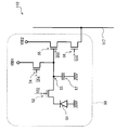
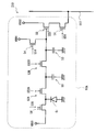
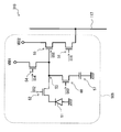
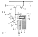
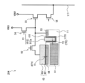
- FIG. 2 illustrates a circuit configuration example of the pixel circuit 50 in one sensor pixel 110 among the plurality of sensor pixels 110 that form the pixel array unit 111.
- the pixel circuit 50 includes a photoelectric conversion unit (PD) 51, a transfer transistor (TG) 52, a charge-voltage conversion unit (FD) 53, a reset transistor (RST) 54, and an amplification transistor (AMP) 55. , A selection transistor (SEL) 56 and a storage capacitor element (CP) 57.
- PD photoelectric conversion unit
- TG transfer transistor
- FD charge-voltage conversion unit
- RST reset transistor
- AMP amplification transistor
- SEL selection transistor
- CP storage capacitor element
- TG52, RST54, AMP55, and SEL56 are all N-type MOS transistors.
- Drive signals S52, S54, S55, and S56 are supplied to the respective gate electrodes of the TG 52, RST 54, AMP 55, and SEL 56 by the vertical drive unit 112 and the horizontal drive unit 114 based on the drive control of the system control unit 115, respectively.
- the drive signals S52, S54, S55, S56 are pulse signals in which a high level state is an active state (on state) and a low level state is an inactive state (off state).
- setting the drive signal to the active state is also referred to as turning on the drive signal
- setting the drive signal to the inactive state is also referred to as turning off the drive signal.
- the PD 51 is, for example, a photoelectric conversion element composed of a PN junction photodiode, and is configured to receive light from a subject and generate and accumulate charges according to the amount of received light by photoelectric conversion.
- the TG52 is connected between the PD51 and the FD53, and is configured to transfer the electric charge accumulated in the PD51 to the FD53 in accordance with the drive signal S52 applied to the gate electrode of the TG52.
- the TG 52 is a specific example corresponding to each of the “first transistor” and the “transfer transistor” of the present disclosure.
- RST54 has, for example, a drain connected to power supply VDD1 and a source connected to FD53.
- the RST 54 initializes, that is, resets the FD 53 according to the drive signal S54 applied to its gate electrode. For example, when the drive signal S54 is turned on and the RST 54 is turned on, the potential of the FD 53 is reset to the voltage level of the power supply VDD1. That is, the FD 53 is initialized.
- the FD 53 is a transfer destination of the charge generated in the PD 51, and is a floating diffusion region that converts the charge transferred from the PD 51 via the TG 52 into an electric signal (for example, a voltage signal) and outputs the electric signal.
- An RST 54 is connected to the FD 53, and a VSL 117 is connected via an AMP 55 and a SEL 56.
- the CP 57 is further connected to the FD 53 via a wiring W57 made of metal or the like (see FIGS. 3 and 4 described later).
- the CP 57 is a storage capacitor element that stores the charges generated in the PD 51 and transferred from the PD 51 together with the FD 53.
- the AMP 55 has, for example, a gate connected to the FD 53, a drain connected to the power supply VDD2, and a source connected to the SEL 56.
- the AMP 55 outputs an electric signal according to the potential of the FD 53.
- the SEL 56 has, for example, a drain connected to the AMP 55 and a source connected to the VSL 117. The SEL 56 is turned on when the sensor pixel 110 is selected, and outputs an electric signal from the FD 53 via the AMP 55 to the column signal processing unit 113 via the VSL 117.
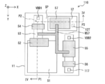
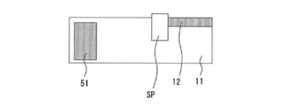
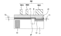
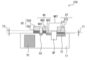
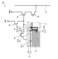
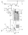
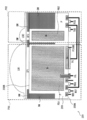
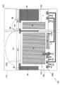
- FIG. 3 illustrates a planar configuration example of one sensor pixel 110 among the plurality of sensor pixels 110 configuring the pixel array section 111.
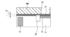
- FIG. 4 shows a cross-sectional configuration example of one sensor pixel 110, and corresponds to a cross section in the direction of the arrow along the IV-IV cutting line shown in FIG.
- the portion from the position P1 to the position P2 shows the YZ cross section along the Y-axis direction
- the portion from the position P2 to the position P3 shows the XZ cross section along the X-axis direction.
- the PD 51 occupies most of the area of the sensor pixel 110, and FD53, RST54, AMP55, SEL56, CP57, power supply VDD1, power supply VDD2 and VSL117 are provided in the peripheral area. It is provided.
- the TG 52 is provided at a position where it partially overlaps the PD 51 in the Z-axis direction (also referred to as the thickness direction or the depth direction).
- the sensor pixel 110 includes a semiconductor layer 11 formed of a semiconductor material such as Si (silicon), a PD 51 provided inside the semiconductor layer 11, and a semiconductor layer 11 on the semiconductor layer 11. And a TG 52 as a transfer unit provided in the.
- the TG 52 includes a laminated structure in which a gate insulating film 521 made of silicon oxide or the like and a gate electrode layer 522 are sequentially laminated on the semiconductor layer 11.
- the RST 54 includes a laminated structure in which a gate insulating film 541 made of silicon oxide or the like and a gate electrode layer 542 are sequentially laminated on the semiconductor layer 11.
- the FD 53 is provided between the TG 52 and the RST 54 in the uppermost part of the semiconductor layer 11.
- the CP 57 includes an insulating film 571 stacked on the impurity diffusion layer 12 provided on the uppermost part of the semiconductor layer 11 and a metal layer 572 stacked on the insulating film 571.
- the FD 53 is connected to the metal layer 572 of the CP 57 via the wiring W57.
- An element isolation part SP is provided between the RST 54 and the CP 57. Note that the description of the element isolation portion SP will be omitted below.
- the impurity diffusion layer 12 is provided with a contact layer 12T (see FIG. 3).
- the insulating film 571 of the CP 57 has the film thickness ET1 as the first electrical film thickness and the film thickness T1 as the first physical film thickness.
- both the gate insulating film 521 of the TG 52 and the gate insulating film 541 of the RST 54 have the film thickness ET2 as the second electrical film thickness and the film thickness T2 as the second physical film thickness.
- the film thickness ET2 is thicker than the film thickness ET1 (ET1 ⁇ ET2).
- the film thickness T2 is preferably thicker than the film thickness T1 (T1 ⁇ T2). That is, the insulating film 571 has a first withstand voltage, and the gate insulating films 521 and 541 have a second withstand voltage higher than the first withstand voltage.
- each gate insulating film in the AMP 55 and the SEL 56 has a film thickness ET2 larger than the film thickness ET1 and a film thickness T2 larger than the film thickness T1.
- the electric film thickness a parameter proportional to the physical thickness of the film divided by the dielectric constant of the film (physical thickness / dielectric constant), for example, an electrical capacitive in terms of SiO 2 EOT (Equivalent oxide thickness) representing a film thickness equivalent to is one specific example.
- SiO 2 EOT Equivalent oxide thickness
- the insulating film 571 of the CP 57, the gate insulating film 521 of the TG 52, and the gate insulating film 541 of the RST 54 may all be made of the same kind of material, that is, materials having the same dielectric constant.
- the dielectric constant of the insulating film 571 of the CP 57 is preferably higher than the dielectric constant of the gate insulating film 521 of the TG 52 or the gate insulating film 541 of the RST 54. This is because the storage capacity of the CP 57, that is, the saturated charge amount per area occupied by the unit pixel can be increased.
- the drive signal S52 to the TG 52 is turned on based on the drive control of the system control unit 115 when reading the electric charge generated and accumulated in the PD 51 that receives the light from the subject.
- the charge accumulated in the PD 51 is transferred from the PD 51 to the FD 53 via the TG 52.
- the FD 53 converts the electric signal into a level electric signal corresponding to each electric charge.
- the SEL 56 is turned on by the drive signal S56, the electric signal from the FD 53 is output to the column signal processing unit 113 through the VSL 117 via the AMP 55 and the SEL 56 in sequence.
- FIGS. 5A to 5G are cross-sectional views showing one step in the method of manufacturing the solid-state imaging device 101A, and are cross-sectional views corresponding to FIG.
- the semiconductor layer 11 in which the PD 51 is embedded is prepared, and the impurity diffusion layer 12 is formed by ion implantation at a predetermined position of the uppermost layer of the semiconductor layer 11.
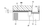
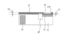
- an insulating material is deposited by, for example, a thermal oxidation method or a sputtering method so as to cover the semiconductor layer 11 over the entire surface to form an insulating film Z1.
- the insulating film Z1 is adjusted to have a predetermined thickness T2.
- a resist mask RM1 having an opening K1 at a position overlapping with a partial region of the impurity diffusion layer 12 is formed on the insulating film Z1.
- an opening Z1K is formed by selectively removing a portion of the insulating film Z1 that is not covered with the resist mask RM1, and a part of the impurity diffusion layer 12 is exposed.
- the insulating film Z2 is selectively formed so as to fill the opening Z1K.
- the insulating film Z2 is obtained by depositing an insulating material by, for example, a thermal oxidation method or a sputtering method. At that time, the insulating film Z2 is adjusted to have a predetermined thickness T1.
- the gate electrode material film M is formed so as to cover the insulating film Z1 and the insulating film Z2. Further, a resist mask RM2 that selectively covers the gate electrode material film M is formed.
- the resist mask RM2 includes portions RM2A to RM2C.
- the part RM2A is formed in a region where the TG 52 is to be formed
- the part RM2A is formed in a region where the RST 54 is to be formed
- the part RM2C is formed in a region where the CP 57 is to be formed.
- the resist mask RM2 is removed.
- a TG 52 in which a gate insulating film 521 and a gate electrode layer 522 were sequentially stacked, a gate insulating film 541 and a gate electrode layer 542 were sequentially stacked on the semiconductor layer 11.
- a CP 57 in which an insulating film 571 and a metal layer 572 are sequentially stacked on the RST 54 and the impurity diffusion layer 12 is obtained.
- the FD 53, the power supply VDD1 and the like are formed at predetermined positions on the uppermost layer of the semiconductor layer 11.
- AMP 55 and SEL 56 are not shown in FIGS. 5A to 5G, AMP 55 and SEL 56 may be formed simultaneously with formation of TG 52 and RST 54 by the same method as TG 52 and RST 54.
- the manufacturing of the solid-state imaging device 101A is completed by, for example, forming the wiring W57.
- the film thickness T2 of each transistor forming the pixel circuit 50 for example, the gate insulating film 521 of the TG 52 and the gate insulating film 541 of the RST 54 in each sensor pixel 110.
- the film thickness T1 (film thickness ET1) of the insulating film 571 of the CP 57 is made smaller than (film thickness ET2). Therefore, in the solid-state imaging device 101A, the saturated charge amount of the CP 57 in each sensor pixel 110 can be improved without increasing the area occupied by the CP 57. That is, in each sensor pixel 110, the saturated charge amount per unit area of the CP 57 becomes large. Therefore, in the solid-state imaging device 101A, for example, the area occupancy of the PD 51 in each sensor pixel 110 can be increased, and high integration of the sensor pixel 110 can be realized.
- the film thickness T2 (film thickness ET2) of the gate insulating film 521 of the TG 52 is made larger than the film thickness T1 (film thickness ET1) of the insulating film 571 of the CP57. Therefore, a higher voltage can be applied to the TG 52, and the charge can be transferred from the PD 51 to the FD 53 more quickly.
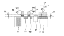
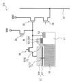
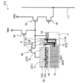
- FIG. 6 illustrates a circuit configuration example of the pixel circuit 50A in the sensor pixel 210 according to the second embodiment of the present technology.
- FIG. 7 illustrates a cross-sectional configuration example of the sensor pixel 210.
- the sensor pixel 210 is mounted on the solid-state imaging device 101A instead of the sensor pixel 110 according to the first embodiment, and realizes a so-called global shutter type image sensor.
- the global shutter method is a method of performing global exposure that basically starts exposure at the same time for all pixels and ends exposure at the same time for all pixels.
- all the pixels mean all the pixels of the part appearing in the image, and dummy pixels and the like are excluded.
- a method of moving the area to be globally exposed while performing global exposure in units of multiple rows (for example, several tens of rows) instead of simultaneously performing all pixels is also possible. It is included in the global shutter system.
- the global shutter system also includes a system in which global exposure is performed on pixels in a predetermined area, instead of all of the pixels in the image.
- the pixel circuit 50A is different from the pixel circuit 50 in that a charge holding unit (MEM) 59 is further provided between the PD 51 and the FD 53 instead of the CP 57. Further, the pixel circuit 50A is different from the pixel circuit 50 in that it has a first transfer transistor (TG) 52A and a second transfer transistor (TG) 52B instead of the TG 52.
- the TG 52A is arranged between the PD 51 and the MEM 59
- the TG 52B is arranged between the MEM 59 and the FD 53.
- the pixel circuit 50A further has a power supply VDD3 as a transfer destination of charges generated in the PD 51, and also has a discharge transistor (OFG) 58 between the PD 51 and the power supply VDD3. Except for these points, the pixel circuit 50A has substantially the same configuration as the pixel circuit 50 according to the above-described first embodiment.
- the power supply VDD3, the impurity diffusion layer 12, the FD 53, the power supply VDD1 and the like are formed in the uppermost layer of the semiconductor layer 11.
- OFG58, TG52A, MEM59, TG52B, RST54, etc. are formed on the semiconductor layer 11.
- the OFG 58 has a drain connected to the power supply VDD3 and a source connected to a wiring connecting the TG 52 and the PD 51.
- the OFG 58 includes a stacked structure in which a gate insulating film 581 made of silicon oxide or the like and a gate electrode layer 582 are sequentially stacked on the semiconductor layer 11.
- the OFG 58 initializes, that is, resets the PD 51 according to the drive signal S58 applied to the gate electrode layer 582. Resetting the PD 51 means depleting the PD 51.
- the OFG 58 forms an overflow path between the TG 52 and the power supply VDD3, and discharges the electric charge overflowing from the PD 51 to the power supply VDD3.
- the FD holding type global shutter in which the OFG 58 can directly reset the PD 51 can be realized.
- the MEM 59 is provided between the PD 51 and the FD 53, and in order to realize the global shutter function, a region that temporarily holds the electric charge generated and accumulated in the PD 51 until it is transferred to the FD 53. Is.
- the MEM 59 includes a stacked structure in which an insulating film 591 made of silicon oxide or the like and a gate electrode layer 592 made of polysilicon or the like are sequentially stacked on the semiconductor layer 11.
- the TG52A is arranged between PD51 and MEM59, and TG52B is arranged between MEM59 and FD53.
- the TG 52A includes a stacked structure in which a gate insulating film 521A made of silicon oxide or the like and a gate electrode layer 522A are sequentially stacked on the semiconductor layer 11.
- the TG 52A is configured to transfer the charge accumulated in the PD 51 to the MEM 59 according to the drive signal S52A applied to the gate electrode layer 522A.
- the TG 52B includes a stacked structure in which a gate insulating film 521B made of silicon oxide or the like and a gate electrode layer 522B are sequentially stacked on the semiconductor layer 11.
- the TG 52B is configured to transfer the charge temporarily held in the MEM 59 to the FD 53 according to the drive signal S52B applied to the gate electrode layer 522B.
- the drive signal S52A is turned off
- the TG52A is turned off
- the drive signal S52B is turned on
- the TG52B is turned on
- the electric charge held in the MEM 59 is transferred to the FD 53 via the TG 52B. It has become.
- the insulating film 591 of the MEM 59 has the film thickness ET1 as the first electrical film thickness and the film thickness T1 as the first physical film thickness.
- the insulating film 591 is a specific example corresponding to the “first insulating film” of the present disclosure.
- the gate insulating film 581 of the OFG 58, the gate insulating film 521A of the TG 52A, the gate insulating film 521B of the TG 52B, and the gate insulating film 541 of the RST 54 all have the film thickness ET2 as the second electrical film thickness.
- the film thickness ET2 is thicker than the film thickness ET1 (ET1 ⁇ ET2).
- the film thickness T2 is thicker than the film thickness T1 (T1 ⁇ T2).
- the gate insulating films 581, 521A, 521B, 541 are one specific example corresponding to the “second insulating film” of the present disclosure.
- Each gate insulating film in the AMP 55 and the SEL 56 has a film thickness ET2 thicker than the film thickness ET1 and a film thickness T2 thicker than the film thickness T1.
- the insulating film 591 and the gate insulating films 581, 521A, 521B, 541 of the MEM 59 may be made of the same material, that is, a material having the same dielectric constant.
- the dielectric constant of the insulating film 591 of the MEM 59 is preferably higher than that of each of the gate insulating films 581, 521A, 521B, and 541. This is because the storage capacity of the MEM 59, that is, the saturated charge amount per area occupied by the unit pixel can be increased.
- the electric charge from the PD 51 is transferred to the MEM 59, and a memory holding type global shutter can be realized.
- the drive signal S52A applied to the gate electrode of the TG 52A is turned on and the TG 52A is turned on, the charge accumulated in the PD 51 is transferred to the MEM 59 via the TG 52A.
- Is becoming The MEM 59 is an area for temporarily holding the electric charge accumulated in the PD 51 in order to realize the global shutter function.
- the TG 52B is configured to transfer the electric charge held in the MEM 59 to the FD 53 according to the drive signal S52B applied to the gate electrode layer 522B of the TG 52B. For example, when the drive signal S52 is turned off, the TG52A is turned off, the drive signal S52B is turned on, and the TG52B is turned on, the electric charge held in the MEM 59 is transferred to the FD 53 via the TG 52B.
- the sensor pixel 210 can improve the saturated charge amount of the MEM 59 without increasing the area occupied by the MEM 59. That is, the saturation charge amount per unit area of the MEM 59 becomes large in each sensor pixel 210. Therefore, in the global shutter type solid-state imaging device including a plurality of the sensor pixels 210, high integration of the sensor pixels 210 can be realized.
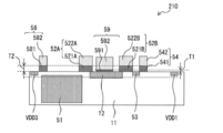
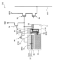
- FIG. 8 illustrates a circuit configuration example of the pixel circuit 50B in the sensor pixel 310 according to the third embodiment of the present technology.
- FIG. 9 illustrates a cross-sectional configuration example of the sensor pixel 310.
- the sensor pixel 310 further includes a switching transistor (FDG) 60 provided between the FD 53 and the CP 57 in addition to the sensor pixel 110 according to the first embodiment. Except for that point, the sensor pixel 310 has substantially the same configuration as the sensor pixel 110.
- the FDG 60 includes, for example, an impurity diffusion layer 603 provided on the uppermost layer of the semiconductor layer 11, a gate insulating film 601 stacked on the semiconductor layer 11, and a gate insulating film 601 on the gate insulating film 601. And a gate electrode layer 602 that is stacked over the gate electrode layer 602.
- the drive signal S60 is supplied to the gate electrode layer 602 by the vertical drive unit 112 and the horizontal drive unit 114 under the drive control of the system control unit 115.
- the FD 53 and the CP 57 are connected.
- the electrical film thickness of the gate insulating film 601 is substantially the same as the film thickness ET2 of the gate insulating film 521 of the TG 52, for example, and is thicker than the film thickness ET1 of the insulating film 571 of the CP 57.
- the physical thickness of the gate insulating film 601 is substantially the same as the film thickness T2 of the gate insulating film 521 of the TG 52, for example. And is thicker than the film thickness T1 of the insulating film 571 of the CP 57.
- the film thickness T1 (film thickness ET1) of the insulating film 571 of the CP 57 is set to the gate insulating film of each transistor forming the pixel circuit 50B, for example, the gate insulating film of TG52. 521 and the gate insulating film 601 of the FDG 60 are made thinner than the film thickness T2 (film thickness ET2). Therefore, the same effect as the sensor pixel 110 according to the first embodiment can be expected.
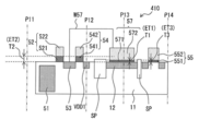
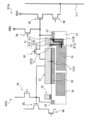
- FIG. 10 shows a planar configuration example of the sensor pixel 410 according to the second embodiment of the present technology.
- FIG. 11 shows a cross-sectional configuration example of the sensor pixel 410, and corresponds to the cross section in the direction of the arrow along the XI-XI cutting line shown in FIG.
- the part from position P11 to position P12 and the part from position P13 to position P14 each show a YZ cross section along the Y-axis direction
- the part from position P12 to position P13 is the X-axis.
- the XZ cross section along the direction is shown.
- the AMP 55 includes a laminated structure in which a gate insulating film 551 made of silicon oxide or the like and a gate electrode layer 552 are sequentially laminated on the semiconductor layer 11.
- the gate insulating film in the AMP 55 has a film thickness T2 (film thickness ET2) larger than the film thickness T1 (film thickness ET1), for example.
- the gate insulating film 551 in the AMP 55 has, for example, the film thickness ET3 as the third electrical film thickness and the film thickness as the third physical film thickness. Having T3.
- the film thickness ET3 of the gate insulating film 551 is thinner than the film thickness ET2 of the gate insulating film 521 of the TG 52, for example. Further, for example, when the respective constituent materials of the gate insulating film 551 and the gate insulating film 521 are the same, that is, when the gate insulating film 551 and the gate insulating film 521 are both made of the material having the same dielectric constant, the gate insulating film 551 Has a thickness T3 smaller than the thickness T2 of the gate insulating film 521.
- FIG. 11 illustrates the case where the film thickness T3 (film thickness ET3) is substantially the same as the film thickness T1 (film thickness ET1), the film thickness T3 (film thickness ET3) is the film thickness T1. It may be different from (film thickness ET1).
- the AMP 55 is one specific example corresponding to the “second transistor” of the present invention
- the gate insulating film 551 is one specific example corresponding to the “third insulating film” of the present disclosure.
- the film thickness T1 (film thickness ET1) of the insulating film 571 of the CP 57 is set to the gate insulating film of each transistor forming the sensor pixel 410, for example, the gate insulating film of TG52. It is made thinner than the film thickness T2 (film thickness ET2) in 521. Therefore, the same effect as the sensor pixel 110 according to the first embodiment can be expected.
- the thickness T3 (thickness ET3) of the gate insulating film 551 in the AMP 55 is equal to the thickness ET2 (thickness ET2 of the gate insulating film 521 of the TG 52 and the gate insulating film 601 of the FDG 60). ) Is thinner than. Therefore, RTS noise (random telegraph signal noise) in the AMP 55 can be reduced.
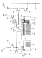
- FIG. 12 shows an example of the overall configuration of a sensor pixel 510 according to the fifth embodiment of the present technology.
- the storage capacitor element (CP) 57 is stacked at a position overlapping the photoelectric conversion unit (PD) 51 in the thickness direction of the semiconductor layer 11.
- CP57 is a MOS capacitor connected to the FDG 60. Except for this point, the sensor pixel 510 has substantially the same configuration as the sensor pixel 310 according to the above-described third embodiment.
- the sensor pixel 510 can switch between low conversion efficiency and high conversion efficiency according to the illuminance of the subject. That is, the capacity of the FD 53 can be switched by the on / off operation of the FDG 60. For example, by turning on the FDG 60, the FD 53 is connected to the CP 57 which is a MOS capacitor. As a result, the capacity of the FD 53 increases and the conversion efficiency decreases.
- the film thickness T1 (film thickness ET1) of the insulating film 571 of the CP 57 is set to the gate insulating film of each transistor forming the sensor pixel 510, for example, the gate insulating film of TG52. 521 and the gate insulating film 601 of the FDG 60 are made thinner than the film thickness T2 (film thickness ET2). Therefore, the same effect as the sensor pixel 110 according to the first embodiment can be expected.
- the CP 57 is laminated on the PD 51, so that the ratio of the formation area of the PD 51 to the area occupied by the sensor pixel 510 can be increased. Therefore, it is advantageous for high integration of the solid-state imaging device.
- FIG. 13 shows an overall configuration example of the sensor pixel 610 according to the sixth embodiment of the present technology.
- the TG 61 is provided instead of the TG 52.
- the TG 61 is a vertical transistor having a gate insulating film 611 and a gate electrode 612 including a plug 612a extending in the thickness direction of the semiconductor layer 11.
- the plug 612a is inserted in a trench 11TR formed in the semiconductor layer 11 and extending in the thickness direction of the semiconductor layer 11.
- a head 612b is provided on the upper end of the plug 612a.
- Gate electrode 612 is separated from semiconductor layer 11 by gate insulating film 611 covering the inner surface of trench 11TR.
- Trench 11TR has a wall surface and a bottom surface which are entirely covered with gate insulating film 611. Except for this point, the sensor pixel 610 has substantially the same configuration as the sensor pixel 510 according to the fifth embodiment described above.
- the TG 61 is a specific example corresponding to the “first transistor” and the “vertical transistor” of the present disclosure.
- the gate insulating film 611 is a specific example corresponding to the “second insulating film” of the present disclosure.
- the minimum value of the film thickness ET1 which is the electric film thickness of the insulating film 571 of the CP 57 is smaller than the minimum value of the film thickness ET2 which is the electric film thickness of the gate insulating film 611. Therefore, for example, when the dielectric constant of the insulating film 571 and the dielectric constant of the gate insulating film 611 are the same, the minimum value of the film thickness T1 which is the physical film thickness of the insulating film 571 of CP57 is the same as that of the gate insulating film 611. The thickness is smaller than the minimum value of the physical thickness T2. Therefore, the same effect as the sensor pixel 110 according to the first embodiment can be expected.
- the vertical transistor TG61 is provided in the sensor pixel 610. Therefore, the plug 612a of the TG 61 can be brought closer to the PD 51. Therefore, it becomes easier to transfer the charges from the PD 51 to the FD 53.
- FIG. 14 shows an overall configuration example of the sensor pixel 710 according to the seventh embodiment of the present technology.
- the sensor pixel 710 further includes, for example, an n + region 64 between the PD 51 and the CP 57. That is, the CP 57 is a plane type n-type MOS capacitor. Except for this point, the sensor pixel 710 has substantially the same configuration as the sensor pixel 610 according to the sixth embodiment described above.
- the minimum value of the film thickness ET1 which is the electric film thickness of the insulating film 571 of the CP 57 is smaller than the minimum value of the film thickness ET2 which is the electric film thickness of the gate insulating film 611. Therefore, for example, when the dielectric constant of the insulating film 571 and the dielectric constant of the gate insulating film 611 are the same, the minimum value of the film thickness T1 which is the physical film thickness of the insulating film 571 of CP57 is the same as that of the gate insulating film 611. The thickness is smaller than the minimum value of the physical thickness T2. Therefore, the same effect as the sensor pixel 110 according to the first embodiment can be expected.
- FIG. 15 shows an example of the overall configuration of a sensor pixel 810 according to the eighth embodiment of the present technology.
- the sensor pixel 810 includes a storage capacitor element (CP) 63 having an insulating film 631 and a conductive layer 632 instead of the CP 57.
- CP storage capacitor element
- a plurality of trenches 64TR are formed in the n + region 64, and the insulating film 631 of CP63 is provided so as to cover the inner surface thereof.
- the conductive layer 632 of CP63 includes a protrusion 632T inserted into the plurality of trenches 64TR. That is, CP63 is a trench type MOS capacitor including an uneven structure.
- the sensor pixel 810 has substantially the same configuration as the sensor pixel 710 according to the seventh embodiment except for these points.
- the minimum value of the film thickness ET1 which is the electrical film thickness of the insulating film 631 of the CP 63 is smaller than the minimum value of the film thickness ET2 which is the electrical film thickness of the gate insulating film 611. Therefore, for example, when the dielectric constant of the insulating film 631 and the dielectric constant of the gate insulating film 611 are the same, the minimum value of the film thickness T1 which is the physical film thickness of the insulating film 631 of CP63 is the minimum value of the gate insulating film 611. The thickness is smaller than the minimum value of the physical thickness T2. Therefore, the same effect as the sensor pixel 110 according to the first embodiment can be expected.
- CP63 including a concavo-convex structure is provided instead of CP57, and the surface area of the insulating film 631 is made larger than the surface area of the insulating film 571. Therefore, the capacitance of CP63 is larger than that of CP57. Can be increased.
- FIG. 16A shows a configuration example of a main part of a solid-state imaging device according to the ninth embodiment of the present technology.
- the solid-state imaging device according to the present embodiment has sensor pixels 910a and sensor pixels 910b arranged so as to be adjacent to each other.
- the sensor pixel 910a has substantially the same configuration as the sensor pixel 710 of the seventh embodiment shown in FIG.
- the sensor pixel 910b is provided in the semiconductor layer 80 adjacent to the semiconductor layer 11, and has a photoelectric conversion unit (PD) 81, a transfer transistor (TG) 82, a charge-voltage conversion unit (FD) 83, a reset transistor (RST) 84, and an amplification.
- PD photoelectric conversion unit
- TG transfer transistor
- FD charge-voltage conversion unit
- RST reset transistor
- PD81, TG82, FD83, RST84, AMP85, and SEL86 have the functions corresponding to PD51, TG52, FD53, RST54, AMP55, and SEL56, respectively. That is, for example, the PD 81 in the sensor pixel 910b is configured to generate electric charge according to the amount of received light by photoelectric conversion, like the PD 51.
- the sensor pixel 910b does not include a storage capacitor element unlike the sensor pixel 910a. Therefore, the CP 57 in the sensor pixel 910a stores not only the charge generated by the PD 51 but also the charge generated by the PD 81.
- the sensitivity of the PD 51 of the sensor pixel 910a is higher than the sensitivity of the PD 81 of the adjacent sensor pixel 910b. That is, the light receiving area of the PD 51 in the sensor pixel 910a is larger than the light receiving area of the PD 81 in the sensor pixel 910b. Therefore, in the solid-state imaging device according to the present embodiment, the sensor pixel 910a including the CP 57 is used as a high sensitivity pixel, and the sensor pixel 910b is used as a low sensitivity pixel, whereby the dynamic range can be expanded.
- the sensor pixel 910b is provided in the semiconductor layer 80 different from the semiconductor layer 11 in the solid-state imaging device shown in FIG. 16A, the sensor pixel 910b may be provided in the same semiconductor layer 11 as the sensor pixel 910a. ..
- the sensor pixel 910a and the sensor pixel 910b share the CP 57.
- the present disclosure is not limited to this.
- the CP 57 does not have to be shared by the sensor pixel 910a and the sensor pixel 910b.
- the FD 53 of the sensor pixel 910a is not connected to the CP 57 of the sensor pixel 910a, but the FD 83 of the sensor pixel 910b is connected.
- the charge generated by the PD 51 of the sensor pixel 910a is not stored in the CP 57, and the charge generated by the PD 81 of the sensor pixel 910b is stored in the CP 57.
- FIG. 17 illustrates a configuration example of a main part of a solid-state imaging device according to the tenth embodiment of the present technology.
- the solid-state imaging device according to the present embodiment includes sensor pixels 910a and sensor pixels 910b arranged adjacent to each other, as in the solid-state imaging device according to the ninth embodiment.
- the sensor pixel 910b is provided in the same semiconductor layer 11 as the sensor pixel 910a.
- CP57 is arranged so as to straddle both PD51 and PD81 in the in-plane direction of semiconductor layer 11, that is, part of CP57 is PD51 and PD81 in the thickness direction of semiconductor layer 11. Is provided in a position overlapping with both. Except for these points, the solid-state imaging device (FIG. 17) of the present embodiment has substantially the same configuration as the solid-state imaging device (FIG. 16) of the ninth embodiment except for these points.
- FIG. 18 is a block diagram showing a configuration example of a camera 2000 as an electronic device to which the present technology is applied.
- the camera 2000 is an optical unit 2001 including a lens group, an imaging device (imaging device) 2002 to which the above-described solid-state imaging device 101 and the like (hereinafter, solid-state imaging device 101 and the like) is applied, and a camera signal processing circuit.
- a DSP (Digital Signal Processor) circuit 2003 is provided.
- the camera 2000 also includes a frame memory 2004, a display unit 2005, a recording unit 2006, an operation unit 2007, and a power supply unit 2008.
- the DSP circuit 2003, the frame memory 2004, the display unit 2005, the recording unit 2006, the operation unit 2007, and the power supply unit 2008 are connected to each other via a bus line 2009.
- the optical unit 2001 captures incident light (image light) from a subject and forms an image on the imaging surface of the imaging device 2002.
- the imaging device 2002 converts the light amount of the incident light imaged on the imaging surface by the optical unit 2001 into an electric signal on a pixel-by-pixel basis and outputs the electric signal as a pixel signal.
- the display unit 2005 includes a panel type display device such as a liquid crystal panel or an organic EL panel, and displays a moving image or a still image captured by the image capturing device 2002.
- the recording unit 2006 records a moving image or a still image captured by the image capturing apparatus 2002 on a recording medium such as a hard disk or a semiconductor memory.
- the operation unit 2007 issues operation commands for various functions of the camera 2000 under the operation of the user.
- the power supply unit 2008 appropriately supplies various power supplies serving as operating power supplies of the DSP circuit 2003, the frame memory 2004, the display unit 2005, the recording unit 2006, and the operation unit 2007 to these supply targets.
- the technology according to the present disclosure (this technology) can be applied to various products.
- the technology according to the present disclosure is realized as a device mounted on any type of moving body such as an automobile, an electric vehicle, a hybrid electric vehicle, a motorcycle, a bicycle, personal mobility, an airplane, a drone, a ship, and a robot. May be.
- FIG. 19 is a block diagram showing a schematic configuration example of a vehicle control system which is an example of a mobile body control system to which the technology according to the present disclosure can be applied.
- the vehicle control system 12000 includes a plurality of electronic control units connected via a communication network 12001.
- the vehicle control system 12000 includes a drive system control unit 12010, a body system control unit 12020, a vehicle exterior information detection unit 12030, a vehicle interior information detection unit 12040, and an integrated control unit 12050.
- a microcomputer 12051, a voice image output unit 12052, and an in-vehicle network I / F (Interface) 12053 are shown as a functional configuration of the integrated control unit 12050.
- the drive system control unit 12010 controls the operation of devices related to the drive system of the vehicle according to various programs.
- the drive system control unit 12010 includes a drive force generation device for generating a drive force of a vehicle such as an internal combustion engine or a drive motor, a drive force transmission mechanism for transmitting the drive force to wheels, and a steering angle of the vehicle. It functions as a steering mechanism for adjusting and a control device such as a braking device for generating a braking force of the vehicle.
- the body system control unit 12020 controls the operation of various devices mounted on the vehicle body according to various programs.
- the body system control unit 12020 functions as a keyless entry system, a smart key system, a power window device, or a control device for various lamps such as a head lamp, a back lamp, a brake lamp, a winker, or a fog lamp.
- the body system control unit 12020 can be input with radio waves or signals of various switches transmitted from a portable device that substitutes for a key.
- the body system control unit 12020 receives input of these radio waves or signals and controls the vehicle door lock device, power window device, lamp, and the like.
- the vehicle exterior information detection unit 12030 detects information outside the vehicle equipped with the vehicle control system 12000.
- the image pickup unit 12031 is connected to the vehicle exterior information detection unit 12030.
- the vehicle exterior information detection unit 12030 causes the image capturing unit 12031 to capture an image of the vehicle exterior and receives the captured image.
- the vehicle exterior information detection unit 12030 may perform object detection processing or distance detection processing such as people, vehicles, obstacles, signs, or characters on the road surface based on the received image.
- the image pickup unit 12031 is an optical sensor that receives light and outputs an electric signal according to the amount of received light.
- the image pickup unit 12031 can output the electric signal as an image or as distance measurement information.
- the light received by the imaging unit 12031 may be visible light or invisible light such as infrared light.
- the in-vehicle information detection unit 12040 detects in-vehicle information.
- a driver state detection unit 12041 that detects the state of the driver is connected.
- the driver state detection unit 12041 includes, for example, a camera that images the driver, and the in-vehicle information detection unit 12040 determines the degree of fatigue or concentration of the driver based on the detection information input from the driver state detection unit 12041. It may be calculated or it may be determined whether or not the driver is asleep.
- the microcomputer 12051 calculates the control target value of the driving force generation device, the steering mechanism or the braking device based on the information on the inside and outside of the vehicle acquired by the outside information detection unit 12030 or the inside information detection unit 12040, and the drive system control unit.
- a control command can be output to 12010.
- the microcomputer 12051 realizes functions of ADAS (Advanced Driver Assistance System) including avoidance or impact mitigation of vehicle collision, follow-up traveling based on inter-vehicle distance, vehicle speed maintenance traveling, vehicle collision warning, vehicle lane departure warning, and the like. It is possible to perform cooperative control for the purpose.
- ADAS Advanced Driver Assistance System
- the microcomputer 12051 controls the driving force generation device, the steering mechanism, the braking device, or the like on the basis of the information around the vehicle acquired by the vehicle exterior information detection unit 12030 or the vehicle interior information detection unit 12040, so that the driver's It is possible to perform cooperative control for the purpose of autonomous driving or the like that autonomously travels without depending on the operation.
- the microcomputer 12051 can output a control command to the body system control unit 12020 based on the information outside the vehicle acquired by the outside information detection unit 12030.
- the microcomputer 12051 controls the headlamp according to the position of the preceding vehicle or the oncoming vehicle detected by the vehicle exterior information detection unit 12030, and performs cooperative control for the purpose of antiglare such as switching the high beam to the low beam. It can be carried out.
- the voice image output unit 12052 transmits an output signal of at least one of a voice and an image to an output device capable of visually or audibly notifying information to a passenger of the vehicle or the outside of the vehicle.
- an audio speaker 12061, a display unit 12062, and an instrument panel 12063 are illustrated as output devices.
- the display unit 12062 may include at least one of an on-board display and a head-up display, for example.
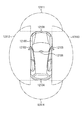
- FIG. 20 is a diagram showing an example of the installation position of the imaging unit 12031.
- the imaging unit 12031 includes imaging units 12101, 12102, 12103, 12104, and 12105.
- the image capturing units 12101, 12102, 12103, 12104, and 12105 are provided at positions such as the front nose of the vehicle 12100, the side mirrors, the rear bumper, the back door, and the upper part of the windshield inside the vehicle.
- the image capturing unit 12101 provided on the front nose and the image capturing unit 12105 provided on the upper part of the windshield in the vehicle interior mainly acquire an image in front of the vehicle 12100.
- the image capturing units 12102 and 12103 provided in the side mirrors mainly acquire images of the side of the vehicle 12100.
- the image capturing unit 12104 provided in the rear bumper or the back door mainly acquires an image behind the vehicle 12100.
- the imaging unit 12105 provided on the upper part of the windshield inside the vehicle is mainly used for detecting a preceding vehicle, a pedestrian, an obstacle, a traffic signal, a traffic sign, a lane, or the like.
- FIG. 20 shows an example of the shooting range of the imaging units 12101 to 12104.
- the imaging range 12111 indicates the imaging range of the imaging unit 12101 provided on the front nose
- the imaging ranges 12112 and 12113 indicate the imaging ranges of the imaging units 12102 and 12103 provided on the side mirrors
- the imaging range 12114 indicates The imaging range of the imaging part 12104 provided in a rear bumper or a back door is shown. For example, by overlaying the image data captured by the image capturing units 12101 to 12104, a bird's-eye view image of the vehicle 12100 viewed from above can be obtained.
- At least one of the imaging units 12101 to 12104 may have a function of acquiring distance information.
- at least one of the image capturing units 12101 to 12104 may be a stereo camera including a plurality of image capturing elements or may be an image capturing element having pixels for phase difference detection.
- the microcomputer 12051 based on the distance information obtained from the imaging units 12101 to 12104, the distance to each three-dimensional object in the imaging range 12111 to 12114 and the temporal change of this distance (relative speed with respect to the vehicle 12100).
- the closest three-dimensional object on the traveling path of the vehicle 12100 which is traveling in the substantially same direction as the vehicle 12100 at a predetermined speed (for example, 0 km / h or more), can be extracted as a preceding vehicle. it can.
- the microcomputer 12051 can set an inter-vehicle distance to be secured in front of the preceding vehicle in advance, and can perform automatic braking control (including follow-up stop control), automatic acceleration control (including follow-up start control), and the like. In this way, it is possible to perform cooperative control for the purpose of autonomous driving, which autonomously travels without depending on the operation of the driver.
- the microcomputer 12051 uses the distance information obtained from the image capturing units 12101 to 12104 to convert three-dimensional object data regarding a three-dimensional object to other three-dimensional objects such as two-wheeled vehicles, ordinary vehicles, large vehicles, pedestrians, telephone poles, and the like. It can be classified, extracted, and used for automatic avoidance of obstacles. For example, the microcomputer 12051 distinguishes obstacles around the vehicle 12100 into obstacles visible to the driver of the vehicle 12100 and obstacles difficult to see. Then, the microcomputer 12051 determines the collision risk indicating the risk of collision with each obstacle, and when the collision risk is equal to or more than the set value and there is a possibility of collision, the microcomputer 12051 outputs the audio through the audio speaker 12061 and the display unit 12062. A driver can be assisted for avoiding a collision by outputting an alarm to the driver and performing forced deceleration or avoidance steering through the drive system control unit 12010.
- At least one of the image capturing units 12101 to 12104 may be an infrared camera that detects infrared rays.
- the microcomputer 12051 can recognize a pedestrian by determining whether or not the pedestrian is present in the images captured by the imaging units 12101 to 12104. To recognize such a pedestrian, for example, a procedure for extracting a feature point in an image captured by the image capturing units 12101 to 12104 as an infrared camera and pattern matching processing on a series of feature points indicating the contour of an object are performed to determine whether or not the pedestrian is a pedestrian.
- the voice image output unit 12052 causes the recognized pedestrian to have a rectangular contour line for emphasis.
- the display unit 12062 is controlled so as to superimpose. Further, the audio image output unit 12052 may control the display unit 12062 to display an icon indicating a pedestrian or the like at a desired position.
- the technology according to the present disclosure can be applied to the imaging unit 12031 among the configurations described above.
- the solid-state imaging device 101A or the like shown in FIG. 1 or the like can be applied to the imaging unit 12031.
- the present disclosure has been described above with reference to some embodiments and modifications, the present disclosure is not limited to the above embodiments and the like, and various modifications are possible.
- the solid-state imaging device of the present disclosure is not limited to those having the pixel circuits described in the above embodiments and the like, and includes those having various pixel circuits.
- FIG. 21A is a cross-sectional view illustrating a configuration example of a main part of a solid-state imaging device 201 as a third modification example of the present disclosure.
- FIG. 21B is a circuit diagram of the solid-state imaging device 201.
- the solid-state imaging device 201 has two sensor pixels PX1 and PX2 arranged so as to be adjacent to each other.
- the sensor pixel PX1 includes a photoelectric conversion unit PD1 embedded in the semiconductor layer 200, a transfer gate TGL provided near the surface 200A of the semiconductor layer 200, a charge / voltage conversion unit FD1, a charge / voltage conversion gate FDG, a reset transistor RST1, It includes an amplification transistor AMP, a selection transistor SEL56 and a floating capacitor FC.
- the sensor pixel PX2 includes a photoelectric conversion unit PD2 embedded in the semiconductor layer 200, a transfer gate TGS and a floating capacitor gate FCG provided near the surface 200A of the semiconductor layer 200.
- the first end of the floating capacitor FC is connected to the power source FCVDD in the sensor pixel PX1
- the second end of the floating capacitor FC is connected to the intermediate portion of the transfer gate TGS and the floating capacitor gate FCG in the sensor pixel PX2.
- the color filter CF1 and the on-chip lens LN1 are sequentially stacked on the back surface 200B of the semiconductor layer 200.
- the color filter CF2 and the on-chip lens LN2 are sequentially stacked on the back surface 200B of the semiconductor layer 200.
- a light shielding film BM is selectively embedded in the color filters CF1 and CF2.
- the light shielding film BM is provided at the boundary between adjacent sensor pixels.
- a light shielding wall BW extending in the thickness direction of the semiconductor layer 200 is provided.
- the light-shielding film BM and the light-shielding wall BW are made of, for example, metal, but are not limited thereto.
- the photoelectric conversion unit PD1 and the floating capacitor FC are stacked so as to overlap each other in the thickness direction of the semiconductor layer 200.
- the transfer gate TGL is a vertical gate extending in the thickness direction of the semiconductor layer 200 up to the photoelectric conversion unit PD1.
- the light shielding film BM is embedded in the color filters CF1 and CF2, but the present disclosure is not limited to this.
- a layer including the color filters CF1 and CF2 may be provided separately from the layer including the light shielding film BM.
- the plug of the gate electrode of the vertical transistor is provided at a position different from the photoelectric conversion unit in plan view, but the present disclosure is not limited to this.
- the gate electrode of the vertical transistor includes the plug and the cap that covers the upper end of the plug, but the present disclosure is not limited thereto. That is, the present disclosure also includes the respective forms shown in FIGS. 23 to 25.
- the plug 612a of the gate electrode 612 of the TG 61 which is a vertical transistor, is positioned so as to overlap the PD 51 in plan view.
- the plug 612a may be inserted into the PD 51.
- the gate electrode 612 of the vertical transistor TG61 does not have the head 612b and has only the plug 612a. May be.
- the gate electrode 612 of the TG 61 that is a vertical transistor does not have the head 612b and has only the plug 612a,
- the plug 612a may be inserted into the PD 51.
- the imaging device of the present disclosure is not limited to the imaging device that detects the light amount distribution of visible light and acquires it as an image, and acquires the distribution of the incident amount of infrared rays, X-rays, particles or the like as an image. It may be an imaging device.
- the solid-state imaging device and the electronic device according to the embodiment of the present disclosure are suitable for high integration of pixels.
- the effect of the present disclosure is not limited to this, and may be any of the effects described below.
- the present technology may have the following configurations. (1) A semiconductor layer, A photoelectric conversion unit which is provided in the semiconductor layer and which generates charges according to the amount of received light by photoelectric conversion, A storage capacitor provided in the semiconductor layer and including a first insulating film having a first electrical thickness; A solid-state imaging device comprising: a first transistor provided in the semiconductor layer, the first transistor including a second insulating film having a second electrical thickness that is thicker than the first electrical thickness.
- the solid-state imaging device according to (1) further including a second transistor including a third insulating film having a third electric film thickness smaller than the second electric film thickness.
- the second transistor is an amplification transistor
- the third insulating film is a gate insulating film of the amplification transistor.
- the storage capacitor element is stacked at a position overlapping the photoelectric conversion unit in a thickness direction of the semiconductor layer.
- the first transistor is a vertical transistor including a gate electrode extending in the thickness direction of the semiconductor layer as a second conductive layer
- the thinnest physical film thickness of the second insulating film is thicker than the thickest physical film thickness of the first insulating film.
- the gate electrode of the vertical transistor has a plug inserted into a trench formed in the semiconductor layer and extending in a thickness direction, The solid-state imaging device according to (5) or (6), wherein the trench has a wall surface and a bottom surface which are entirely covered with the second insulating film.
- the storage capacitor element is a MOS capacitor.
- the solid-state imaging device according to any one of (1) to (7) above.
- the storage capacitor element stores the electric charge generated by the photoelectric conversion unit.
- the adjacent pixel has an adjacent photoelectric conversion unit that generates a charge according to the amount of received light by photoelectric conversion
- the storage capacitor element is provided so as to extend over both the photoelectric conversion section and the adjacent photoelectric conversion section in the in-plane direction of the semiconductor layer.
- the solid-state imaging device according to (12) or (13) above, wherein the sensitivity of the photoelectric conversion unit is higher than the sensitivity of the adjacent photoelectric conversion unit.
- 15) Further comprising an adjacent pixel provided in the semiconductor layer so as to be adjacent to a pixel including the photoelectric conversion unit and the storage capacitor element, The adjacent pixel has an adjacent photoelectric conversion unit that generates a charge according to the amount of received light by photoelectric conversion,
- the solid-state imaging device according to any one of (1) to (11), wherein the storage capacitor element stores the electric charge generated by the adjacent photoelectric conversion unit.
- the first transistor is a transfer transistor that transfers the charges from the photoelectric conversion unit to a transfer destination.
- the solid-state imaging device according to any one of (1) to (15).
- a charge-voltage converter that is provided in the semiconductor layer and that converts the electric charge generated in the photoelectric conversion unit into a voltage, as the transfer destination.
- the storage capacitor element is A charge as the transfer destination, which is provided between the photoelectric conversion unit and the charge-voltage conversion unit, and temporarily holds the charge generated by the photoelectric conversion unit before transferring the charge to the charge-voltage conversion unit.
- the solid-state imaging device according to any one of (17) to (19), further including a switching unit that performs the switching.
- the first physical film thickness of the first insulating film is thinner than the second physical film thickness of the second insulating film.
- a semiconductor layer A photoelectric conversion unit which is provided in the semiconductor layer and which generates electric charges according to the amount of received light by photoelectric conversion,
- a storage capacitor provided in the semiconductor layer and including a first insulating film having a first withstand voltage;
- a solid-state imaging device comprising: a first transistor provided in the semiconductor layer, the first transistor including a second insulating film having a second withstand voltage higher than the first withstand voltage.
- An electronic device including a solid-state imaging device, The solid-state imaging device, A semiconductor layer, A photoelectric conversion unit which is provided in the semiconductor layer and which generates electric charges according to the amount of received light by photoelectric conversion, A storage capacitor element that is provided in the semiconductor layer and includes a first insulating film having a first electrical thickness; A first transistor provided in the semiconductor layer, the first transistor including a second insulating film having a second electric film thickness larger than the first electric film thickness.
Landscapes
- Engineering & Computer Science (AREA)
- Multimedia (AREA)
- Signal Processing (AREA)
- Solid State Image Pick-Up Elements (AREA)
- Transforming Light Signals Into Electric Signals (AREA)
Priority Applications (5)
| Application Number | Priority Date | Filing Date | Title |
|---|---|---|---|
| US17/293,132 US12490529B2 (en) | 2018-11-19 | 2019-11-19 | Solid-state imaging device and electronic apparatus having a storage capacitor with a thin insulating film |
| JP2020557557A JP7520721B2 (ja) | 2018-11-19 | 2019-11-19 | 固体撮像装置および電子機器 |
| CN201980073682.XA CN112970117A (zh) | 2018-11-19 | 2019-11-19 | 固态成像装置和电子设备 |
| DE112019005789.8T DE112019005789T5 (de) | 2018-11-19 | 2019-11-19 | Festkörperbildgebungsvorrichtung und elektronische Einrichtung |
| KR1020217011466A KR102861849B1 (ko) | 2018-11-19 | 2019-11-19 | 고체 촬상 장치 및 전자 기기 |
Applications Claiming Priority (4)
| Application Number | Priority Date | Filing Date | Title |
|---|---|---|---|
| JP2018216342 | 2018-11-19 | ||
| JP2018-216342 | 2018-11-19 | ||
| JP2019206785 | 2019-11-15 | ||
| JP2019-206785 | 2019-11-15 |
Publications (1)
| Publication Number | Publication Date |
|---|---|
| WO2020105634A1 true WO2020105634A1 (ja) | 2020-05-28 |
Family
ID=70773125
Family Applications (1)
| Application Number | Title | Priority Date | Filing Date |
|---|---|---|---|
| PCT/JP2019/045276 Ceased WO2020105634A1 (ja) | 2018-11-19 | 2019-11-19 | 固体撮像装置および電子機器 |
Country Status (7)
| Country | Link |
|---|---|
| US (1) | US12490529B2 (enExample) |
| JP (1) | JP7520721B2 (enExample) |
| KR (1) | KR102861849B1 (enExample) |
| CN (1) | CN112970117A (enExample) |
| DE (1) | DE112019005789T5 (enExample) |
| TW (1) | TWI835928B (enExample) |
| WO (1) | WO2020105634A1 (enExample) |
Cited By (3)
| Publication number | Priority date | Publication date | Assignee | Title |
|---|---|---|---|---|
| WO2021131844A1 (ja) * | 2019-12-25 | 2021-07-01 | ソニーセミコンダクタソリューションズ株式会社 | 受光素子及び受光装置 |
| WO2023074381A1 (ja) * | 2021-10-26 | 2023-05-04 | ソニーセミコンダクタソリューションズ株式会社 | 撮像素子、電子機器 |
| WO2024043068A1 (ja) * | 2022-08-22 | 2024-02-29 | ソニーセミコンダクタソリューションズ株式会社 | 固体撮像素子および電子機器 |
Families Citing this family (1)
| Publication number | Priority date | Publication date | Assignee | Title |
|---|---|---|---|---|
| WO2022059132A1 (ja) * | 2020-09-17 | 2022-03-24 | キオクシア株式会社 | 半導体記憶装置 |
Citations (6)
| Publication number | Priority date | Publication date | Assignee | Title |
|---|---|---|---|---|
| JP2005347655A (ja) * | 2004-06-07 | 2005-12-15 | Canon Inc | 固体撮像装置 |
| JP2009283552A (ja) * | 2008-05-20 | 2009-12-03 | Panasonic Corp | 固体撮像素子 |
| JP2010109136A (ja) * | 2008-10-30 | 2010-05-13 | Sony Corp | 固体撮像装置、その製造方法および撮像装置 |
| JP2013161868A (ja) * | 2012-02-02 | 2013-08-19 | Sony Corp | 固体撮像装置、固体撮像装置の製造方法、及び、電子機器 |
| WO2015068315A1 (ja) * | 2013-11-08 | 2015-05-14 | パナソニックIpマネジメント株式会社 | 固体撮像装置 |
| WO2015152297A1 (ja) * | 2014-03-31 | 2015-10-08 | 株式会社ニコン | 検出素子、ロックイン検出装置、基板、および検出素子の製造方法 |
Family Cites Families (7)
| Publication number | Priority date | Publication date | Assignee | Title |
|---|---|---|---|---|
| JP2000349259A (ja) * | 1999-06-09 | 2000-12-15 | Sanyo Electric Co Ltd | 半導体装置及びその製造方法 |
| KR100738516B1 (ko) * | 2006-05-25 | 2007-07-11 | (주) 픽셀플러스 | 커플링 캐패시터를 사용하는 핀드 포토다이오드를 포함하는액티브 픽셀 및 그의 신호 감지 방법 |
| JP2012129799A (ja) * | 2010-12-15 | 2012-07-05 | Sony Corp | 固体撮像素子および駆動方法、並びに電子機器 |
| US9490373B2 (en) | 2012-02-02 | 2016-11-08 | Sony Corporation | Solid-state imaging device and electronic apparatus with improved storage portion |
| CN103258829A (zh) | 2012-02-16 | 2013-08-21 | 索尼公司 | 固态成像装置、图像传感器及其制造方法以及电子设备 |
| CN108807434B (zh) * | 2017-04-26 | 2023-12-05 | 松下知识产权经营株式会社 | 摄像装置及照相机系统 |
| JP7100315B2 (ja) | 2018-05-30 | 2022-07-13 | 三菱瓦斯化学株式会社 | 漂白パルプの製造方法 |
-
2019
- 2019-11-19 CN CN201980073682.XA patent/CN112970117A/zh active Pending
- 2019-11-19 US US17/293,132 patent/US12490529B2/en active Active
- 2019-11-19 DE DE112019005789.8T patent/DE112019005789T5/de active Pending
- 2019-11-19 WO PCT/JP2019/045276 patent/WO2020105634A1/ja not_active Ceased
- 2019-11-19 TW TW108142022A patent/TWI835928B/zh active
- 2019-11-19 JP JP2020557557A patent/JP7520721B2/ja active Active
- 2019-11-19 KR KR1020217011466A patent/KR102861849B1/ko active Active
Patent Citations (6)
| Publication number | Priority date | Publication date | Assignee | Title |
|---|---|---|---|---|
| JP2005347655A (ja) * | 2004-06-07 | 2005-12-15 | Canon Inc | 固体撮像装置 |
| JP2009283552A (ja) * | 2008-05-20 | 2009-12-03 | Panasonic Corp | 固体撮像素子 |
| JP2010109136A (ja) * | 2008-10-30 | 2010-05-13 | Sony Corp | 固体撮像装置、その製造方法および撮像装置 |
| JP2013161868A (ja) * | 2012-02-02 | 2013-08-19 | Sony Corp | 固体撮像装置、固体撮像装置の製造方法、及び、電子機器 |
| WO2015068315A1 (ja) * | 2013-11-08 | 2015-05-14 | パナソニックIpマネジメント株式会社 | 固体撮像装置 |
| WO2015152297A1 (ja) * | 2014-03-31 | 2015-10-08 | 株式会社ニコン | 検出素子、ロックイン検出装置、基板、および検出素子の製造方法 |
Cited By (4)
| Publication number | Priority date | Publication date | Assignee | Title |
|---|---|---|---|---|
| WO2021131844A1 (ja) * | 2019-12-25 | 2021-07-01 | ソニーセミコンダクタソリューションズ株式会社 | 受光素子及び受光装置 |
| US12382738B2 (en) | 2019-12-25 | 2025-08-05 | Sony Semiconductor Solutions Corporation | Light receiving element and light receiving device |
| WO2023074381A1 (ja) * | 2021-10-26 | 2023-05-04 | ソニーセミコンダクタソリューションズ株式会社 | 撮像素子、電子機器 |
| WO2024043068A1 (ja) * | 2022-08-22 | 2024-02-29 | ソニーセミコンダクタソリューションズ株式会社 | 固体撮像素子および電子機器 |
Also Published As
| Publication number | Publication date |
|---|---|
| KR102861849B1 (ko) | 2025-09-22 |
| DE112019005789T5 (de) | 2021-09-02 |
| US12490529B2 (en) | 2025-12-02 |
| US20220013557A1 (en) | 2022-01-13 |
| TW202029489A (zh) | 2020-08-01 |
| JP7520721B2 (ja) | 2024-07-23 |
| TWI835928B (zh) | 2024-03-21 |
| JPWO2020105634A1 (ja) | 2021-09-30 |
| KR20210093859A (ko) | 2021-07-28 |
| CN112970117A (zh) | 2021-06-15 |
Similar Documents
| Publication | Publication Date | Title |
|---|---|---|
| JP2022161980A (ja) | 撮像素子、撮像素子の製造方法、及び、電子機器 | |
| TWI865651B (zh) | 固體攝像裝置及電子機器 | |
| JP7605732B2 (ja) | 撮像装置および電子機器 | |
| JP7520721B2 (ja) | 固体撮像装置および電子機器 | |
| US11516418B2 (en) | Solid-state imaging apparatus | |
| US11997400B2 (en) | Imaging element and electronic apparatus | |
| US20220159208A1 (en) | Imaging device and electronic apparatus | |
| JP2020047826A (ja) | 固体撮像装置および電子機器 | |
| WO2022249575A1 (ja) | 固体撮像素子、固体撮像素子の製造方法および電子機器 | |
| CN112602195B (zh) | 摄像装置和电子设备 | |
| US20250006758A1 (en) | Imaging element and electronic apparatus | |
| JP2022131910A (ja) | 撮像装置および電子機器 | |
| US20220239849A1 (en) | Imaging device and electronic apparatus | |
| CN118975267A (zh) | 固体摄像装置与电子设备 | |
| JP2020043413A (ja) | 固体撮像装置および電子機器 | |
| WO2023127512A1 (ja) | 撮像装置、電子機器 | |
| WO2020149181A1 (ja) | 撮像装置 | |
| WO2024095630A1 (ja) | 撮像装置 | |
| WO2026004392A1 (ja) | 固体撮像素子 | |
| WO2022080124A1 (ja) | 撮像装置および撮像装置の製造方法 | |
| JP2025019415A (ja) | 撮像素子および電子機器 | |
| JP2025016041A (ja) | 光検出装置 | |
| WO2022201898A1 (ja) | 撮像素子および撮像装置 |
Legal Events
| Date | Code | Title | Description |
|---|---|---|---|
| 121 | Ep: the epo has been informed by wipo that ep was designated in this application |
Ref document number: 19886372 Country of ref document: EP Kind code of ref document: A1 |
|
| ENP | Entry into the national phase |
Ref document number: 2020557557 Country of ref document: JP Kind code of ref document: A |
|
| 122 | Ep: pct application non-entry in european phase |
Ref document number: 19886372 Country of ref document: EP Kind code of ref document: A1 |