WO2020105634A1 - Solid-state imaging device and electronic equipment - Google Patents
Solid-state imaging device and electronic equipmentInfo
- Publication number
- WO2020105634A1 WO2020105634A1 PCT/JP2019/045276 JP2019045276W WO2020105634A1 WO 2020105634 A1 WO2020105634 A1 WO 2020105634A1 JP 2019045276 W JP2019045276 W JP 2019045276W WO 2020105634 A1 WO2020105634 A1 WO 2020105634A1
- Authority
- WO
- WIPO (PCT)
- Prior art keywords
- imaging device
- solid
- state imaging
- insulating film
- photoelectric conversion
- Prior art date
Links
- 238000003384 imaging method Methods 0.000 title claims abstract description 184
- 239000004065 semiconductor Substances 0.000 claims abstract description 97
- 238000006243 chemical reaction Methods 0.000 claims abstract description 89
- 239000003990 capacitor Substances 0.000 claims abstract description 69
- 238000003860 storage Methods 0.000 claims abstract description 53
- 238000012546 transfer Methods 0.000 claims description 32
- 230000003321 amplification Effects 0.000 claims description 8
- 238000003199 nucleic acid amplification method Methods 0.000 claims description 8
- 230000035945 sensitivity Effects 0.000 claims description 8
- 230000010354 integration Effects 0.000 abstract description 8
- 238000012545 processing Methods 0.000 description 36
- 238000001514 detection method Methods 0.000 description 23
- 238000010586 diagram Methods 0.000 description 22
- 238000005516 engineering process Methods 0.000 description 22
- 238000012986 modification Methods 0.000 description 18
- 230000004048 modification Effects 0.000 description 18
- 238000000034 method Methods 0.000 description 15
- 230000000875 corresponding effect Effects 0.000 description 14
- 230000000694 effects Effects 0.000 description 13
- 230000006870 function Effects 0.000 description 11
- 238000009792 diffusion process Methods 0.000 description 9
- 239000012535 impurity Substances 0.000 description 8
- 239000000463 material Substances 0.000 description 8
- VYPSYNLAJGMNEJ-UHFFFAOYSA-N Silicium dioxide Chemical compound O=[Si]=O VYPSYNLAJGMNEJ-UHFFFAOYSA-N 0.000 description 7
- 238000013500 data storage Methods 0.000 description 7
- 238000007667 floating Methods 0.000 description 7
- 229910052814 silicon oxide Inorganic materials 0.000 description 7
- 102100036285 25-hydroxyvitamin D-1 alpha hydroxylase, mitochondrial Human genes 0.000 description 6
- 101000875403 Homo sapiens 25-hydroxyvitamin D-1 alpha hydroxylase, mitochondrial Proteins 0.000 description 6
- 230000008569 process Effects 0.000 description 6
- 238000004519 manufacturing process Methods 0.000 description 5
- 239000002184 metal Substances 0.000 description 5
- 229920006395 saturated elastomer Polymers 0.000 description 5
- 230000007246 mechanism Effects 0.000 description 4
- 230000003287 optical effect Effects 0.000 description 4
- 102220468073 Trafficking protein particle complex subunit 5_S52A_mutation Human genes 0.000 description 3
- 239000007772 electrode material Substances 0.000 description 3
- 238000009825 accumulation Methods 0.000 description 2
- 230000015572 biosynthetic process Effects 0.000 description 2
- 239000000470 constituent Substances 0.000 description 2
- 238000005520 cutting process Methods 0.000 description 2
- 238000009826 distribution Methods 0.000 description 2
- 238000009434 installation Methods 0.000 description 2
- 239000011810 insulating material Substances 0.000 description 2
- 238000005468 ion implantation Methods 0.000 description 2
- 238000002955 isolation Methods 0.000 description 2
- 230000003647 oxidation Effects 0.000 description 2
- 238000007254 oxidation reaction Methods 0.000 description 2
- 230000002093 peripheral effect Effects 0.000 description 2
- 238000004544 sputter deposition Methods 0.000 description 2
- 238000010408 sweeping Methods 0.000 description 2
- 101100041125 Arabidopsis thaliana RST1 gene Proteins 0.000 description 1
- 240000004050 Pentaglottis sempervirens Species 0.000 description 1
- 235000004522 Pentaglottis sempervirens Nutrition 0.000 description 1
- 101100443250 Saccharomyces cerevisiae (strain ATCC 204508 / S288c) DIG1 gene Proteins 0.000 description 1
- 229910004298 SiO 2 Inorganic materials 0.000 description 1
- 230000001133 acceleration Effects 0.000 description 1
- 230000005540 biological transmission Effects 0.000 description 1
- 230000008859 change Effects 0.000 description 1
- 238000002485 combustion reaction Methods 0.000 description 1
- 238000004891 communication Methods 0.000 description 1
- 230000000295 complement effect Effects 0.000 description 1
- 230000002596 correlated effect Effects 0.000 description 1
- 230000007423 decrease Effects 0.000 description 1
- 230000000779 depleting effect Effects 0.000 description 1
- 238000000151 deposition Methods 0.000 description 1
- 238000013461 design Methods 0.000 description 1
- 239000004973 liquid crystal related substance Substances 0.000 description 1
- 238000012423 maintenance Methods 0.000 description 1
- 238000005259 measurement Methods 0.000 description 1
- 229910044991 metal oxide Inorganic materials 0.000 description 1
- 150000004706 metal oxides Chemical class 0.000 description 1
- 230000000116 mitigating effect Effects 0.000 description 1
- 239000002245 particle Substances 0.000 description 1
- 238000000206 photolithography Methods 0.000 description 1
- 229910021420 polycrystalline silicon Inorganic materials 0.000 description 1
- 229920005591 polysilicon Polymers 0.000 description 1
- 238000005070 sampling Methods 0.000 description 1
- 229910052710 silicon Inorganic materials 0.000 description 1
- 239000010703 silicon Substances 0.000 description 1
- 239000007787 solid Substances 0.000 description 1
- 230000002123 temporal effect Effects 0.000 description 1
- -1 that is Substances 0.000 description 1
Images


Classifications
-
- H—ELECTRICITY
- H01—ELECTRIC ELEMENTS
- H01L—SEMICONDUCTOR DEVICES NOT COVERED BY CLASS H10
- H01L27/00—Devices consisting of a plurality of semiconductor or other solid-state components formed in or on a common substrate
- H01L27/14—Devices consisting of a plurality of semiconductor or other solid-state components formed in or on a common substrate including semiconductor components sensitive to infrared radiation, light, electromagnetic radiation of shorter wavelength or corpuscular radiation and specially adapted either for the conversion of the energy of such radiation into electrical energy or for the control of electrical energy by such radiation
- H01L27/144—Devices controlled by radiation
- H01L27/146—Imager structures
- H01L27/14601—Structural or functional details thereof
- H01L27/14609—Pixel-elements with integrated switching, control, storage or amplification elements
- H01L27/14612—Pixel-elements with integrated switching, control, storage or amplification elements involving a transistor
-
- H—ELECTRICITY
- H01—ELECTRIC ELEMENTS
- H01L—SEMICONDUCTOR DEVICES NOT COVERED BY CLASS H10
- H01L27/00—Devices consisting of a plurality of semiconductor or other solid-state components formed in or on a common substrate
- H01L27/14—Devices consisting of a plurality of semiconductor or other solid-state components formed in or on a common substrate including semiconductor components sensitive to infrared radiation, light, electromagnetic radiation of shorter wavelength or corpuscular radiation and specially adapted either for the conversion of the energy of such radiation into electrical energy or for the control of electrical energy by such radiation
- H01L27/144—Devices controlled by radiation
- H01L27/146—Imager structures
- H01L27/14601—Structural or functional details thereof
- H01L27/14609—Pixel-elements with integrated switching, control, storage or amplification elements
-
- H—ELECTRICITY
- H01—ELECTRIC ELEMENTS
- H01L—SEMICONDUCTOR DEVICES NOT COVERED BY CLASS H10
- H01L27/00—Devices consisting of a plurality of semiconductor or other solid-state components formed in or on a common substrate
- H01L27/14—Devices consisting of a plurality of semiconductor or other solid-state components formed in or on a common substrate including semiconductor components sensitive to infrared radiation, light, electromagnetic radiation of shorter wavelength or corpuscular radiation and specially adapted either for the conversion of the energy of such radiation into electrical energy or for the control of electrical energy by such radiation
- H01L27/144—Devices controlled by radiation
- H01L27/146—Imager structures
- H01L27/14601—Structural or functional details thereof
- H01L27/14603—Special geometry or disposition of pixel-elements, address-lines or gate-electrodes
- H01L27/14605—Structural or functional details relating to the position of the pixel elements, e.g. smaller pixel elements in the center of the imager compared to pixel elements at the periphery
-
- H—ELECTRICITY
- H01—ELECTRIC ELEMENTS
- H01L—SEMICONDUCTOR DEVICES NOT COVERED BY CLASS H10
- H01L27/00—Devices consisting of a plurality of semiconductor or other solid-state components formed in or on a common substrate
- H01L27/14—Devices consisting of a plurality of semiconductor or other solid-state components formed in or on a common substrate including semiconductor components sensitive to infrared radiation, light, electromagnetic radiation of shorter wavelength or corpuscular radiation and specially adapted either for the conversion of the energy of such radiation into electrical energy or for the control of electrical energy by such radiation
- H01L27/144—Devices controlled by radiation
- H01L27/146—Imager structures
- H01L27/14601—Structural or functional details thereof
- H01L27/14603—Special geometry or disposition of pixel-elements, address-lines or gate-electrodes
-
- H—ELECTRICITY
- H01—ELECTRIC ELEMENTS
- H01L—SEMICONDUCTOR DEVICES NOT COVERED BY CLASS H10
- H01L27/00—Devices consisting of a plurality of semiconductor or other solid-state components formed in or on a common substrate
- H01L27/14—Devices consisting of a plurality of semiconductor or other solid-state components formed in or on a common substrate including semiconductor components sensitive to infrared radiation, light, electromagnetic radiation of shorter wavelength or corpuscular radiation and specially adapted either for the conversion of the energy of such radiation into electrical energy or for the control of electrical energy by such radiation
- H01L27/144—Devices controlled by radiation
- H01L27/146—Imager structures
- H01L27/14601—Structural or functional details thereof
- H01L27/1463—Pixel isolation structures
-
- H—ELECTRICITY
- H01—ELECTRIC ELEMENTS
- H01L—SEMICONDUCTOR DEVICES NOT COVERED BY CLASS H10
- H01L27/00—Devices consisting of a plurality of semiconductor or other solid-state components formed in or on a common substrate
- H01L27/14—Devices consisting of a plurality of semiconductor or other solid-state components formed in or on a common substrate including semiconductor components sensitive to infrared radiation, light, electromagnetic radiation of shorter wavelength or corpuscular radiation and specially adapted either for the conversion of the energy of such radiation into electrical energy or for the control of electrical energy by such radiation
- H01L27/144—Devices controlled by radiation
- H01L27/146—Imager structures
- H01L27/14601—Structural or functional details thereof
- H01L27/14636—Interconnect structures
-
- H—ELECTRICITY
- H01—ELECTRIC ELEMENTS
- H01L—SEMICONDUCTOR DEVICES NOT COVERED BY CLASS H10
- H01L27/00—Devices consisting of a plurality of semiconductor or other solid-state components formed in or on a common substrate
- H01L27/14—Devices consisting of a plurality of semiconductor or other solid-state components formed in or on a common substrate including semiconductor components sensitive to infrared radiation, light, electromagnetic radiation of shorter wavelength or corpuscular radiation and specially adapted either for the conversion of the energy of such radiation into electrical energy or for the control of electrical energy by such radiation
- H01L27/144—Devices controlled by radiation
- H01L27/146—Imager structures
- H01L27/14643—Photodiode arrays; MOS imagers
-
- H—ELECTRICITY
- H04—ELECTRIC COMMUNICATION TECHNIQUE
- H04N—PICTORIAL COMMUNICATION, e.g. TELEVISION
- H04N25/00—Circuitry of solid-state image sensors [SSIS]; Control thereof
- H04N25/70—SSIS architectures; Circuits associated therewith
- H04N25/76—Addressed sensors, e.g. MOS or CMOS sensors
- H04N25/77—Pixel circuitry, e.g. memories, A/D converters, pixel amplifiers, shared circuits or shared components
-
- H—ELECTRICITY
- H01—ELECTRIC ELEMENTS
- H01L—SEMICONDUCTOR DEVICES NOT COVERED BY CLASS H10
- H01L27/00—Devices consisting of a plurality of semiconductor or other solid-state components formed in or on a common substrate
- H01L27/14—Devices consisting of a plurality of semiconductor or other solid-state components formed in or on a common substrate including semiconductor components sensitive to infrared radiation, light, electromagnetic radiation of shorter wavelength or corpuscular radiation and specially adapted either for the conversion of the energy of such radiation into electrical energy or for the control of electrical energy by such radiation
- H01L27/144—Devices controlled by radiation
- H01L27/146—Imager structures
- H01L27/14601—Structural or functional details thereof
- H01L27/1462—Coatings
- H01L27/14621—Colour filter arrangements
-
- H—ELECTRICITY
- H01—ELECTRIC ELEMENTS
- H01L—SEMICONDUCTOR DEVICES NOT COVERED BY CLASS H10
- H01L27/00—Devices consisting of a plurality of semiconductor or other solid-state components formed in or on a common substrate
- H01L27/14—Devices consisting of a plurality of semiconductor or other solid-state components formed in or on a common substrate including semiconductor components sensitive to infrared radiation, light, electromagnetic radiation of shorter wavelength or corpuscular radiation and specially adapted either for the conversion of the energy of such radiation into electrical energy or for the control of electrical energy by such radiation
- H01L27/144—Devices controlled by radiation
- H01L27/146—Imager structures
- H01L27/14601—Structural or functional details thereof
- H01L27/1462—Coatings
- H01L27/14623—Optical shielding
-
- H—ELECTRICITY
- H01—ELECTRIC ELEMENTS
- H01L—SEMICONDUCTOR DEVICES NOT COVERED BY CLASS H10
- H01L27/00—Devices consisting of a plurality of semiconductor or other solid-state components formed in or on a common substrate
- H01L27/14—Devices consisting of a plurality of semiconductor or other solid-state components formed in or on a common substrate including semiconductor components sensitive to infrared radiation, light, electromagnetic radiation of shorter wavelength or corpuscular radiation and specially adapted either for the conversion of the energy of such radiation into electrical energy or for the control of electrical energy by such radiation
- H01L27/144—Devices controlled by radiation
- H01L27/146—Imager structures
- H01L27/14683—Processes or apparatus peculiar to the manufacture or treatment of these devices or parts thereof
- H01L27/14689—MOS based technologies
Definitions
- the present disclosure relates to a solid-state imaging device that performs imaging by performing photoelectric conversion, and an electronic device including the solid-state imaging device.
- a solid-state imaging device includes a semiconductor layer, a photoelectric conversion unit that is provided in the semiconductor layer and generates a charge according to the amount of received light by photoelectric conversion, and a first electrical element provided in the semiconductor layer.
- a storage capacitor element including a first insulating film having a film thickness, and a first insulating film provided in the semiconductor layer and having a second electric film thickness larger than the first electric film thickness.
- a transistor a transistor.
- the insulating film of the storage capacitor can be thinned by the above configuration, so that the capacitance of the storage capacitor can be increased without expanding the area occupied by the storage capacitor. To do.
- FIG. 3 is a block diagram showing a configuration example of functions of the solid-state imaging device according to the first embodiment of the present disclosure. It is a block diagram which shows the structural example of a function of the solid-state imaging device as a 1st modification. It is a block diagram which shows the structural example of the function of the solid-state imaging device as a 2nd modification.
- FIG. 1B is a circuit diagram showing a circuit configuration example of one sensor pixel in the solid-state imaging device shown in FIG. 1A.
- FIG. 3 is a plan view illustrating a planar configuration example of the sensor pixel illustrated in FIG. 2.
- FIG. 3 is a cross-sectional view showing a cross-sectional configuration example of the sensor pixel shown in FIG. 2.
- FIG. 1B is a circuit diagram showing a circuit configuration example of one sensor pixel in the solid-state imaging device shown in FIG. 1A.
- FIG. 3 is a plan view illustrating a planar configuration example of the sensor pixel illustrated in FIG. 2.
- FIG. 9 is a cross-sectional view showing a step in the method of manufacturing the sensor pixel shown in FIG. 2. It is sectional drawing showing 1 process following FIG. 5A. It is sectional drawing showing 1 process following FIG. 5B.
- FIG. 5C is a cross-sectional view showing a process following FIG. 5C. It is sectional drawing showing 1 process following FIG. 5D.
- FIG. 5C is a cross-sectional view showing a process following FIG. 5E. It is sectional drawing showing 1 process of following FIG. 5F.
- FIG. 16 is a circuit diagram illustrating a circuit configuration example of one sensor pixel in the solid-state imaging device according to the second embodiment of the present disclosure.
- FIG. 16 is a circuit diagram illustrating a circuit configuration example of one sensor pixel in the solid-state imaging device according to the second embodiment of the present disclosure.
- FIG. 7 is an explanatory diagram including a partial cross-sectional configuration example of the sensor pixel shown in FIG. 6.
- FIG. 16 is a circuit diagram illustrating a circuit configuration example of one sensor pixel in the solid-state imaging device according to the third embodiment of the present disclosure.
- FIG. 9 is an explanatory diagram including a partial cross-sectional configuration example of the sensor pixel shown in FIG. 8.
- FIG. 16 is a plan view illustrating a planar configuration example of one sensor pixel in a solid-state imaging device according to a fourth embodiment of the present disclosure.
- FIG. 11 is a cross-sectional view illustrating a cross-sectional configuration example of the sensor pixel illustrated in FIG. 10.
- FIG. 16 is an explanatory diagram including a cross-sectional configuration example of one sensor pixel in a solid-state imaging device according to a fifth embodiment of the present disclosure. It is explanatory drawing containing the example of a cross-sectional structure of one sensor pixel in the solid-state imaging device concerning 6th Embodiment of this indication.
- FIG. 16 is an explanatory diagram including a cross-sectional configuration example of one sensor pixel in a solid-state imaging device according to a seventh embodiment of the present disclosure. It is explanatory drawing including the example of a cross-sectional structure of one sensor pixel in the solid-state imaging device which concerns on 8th Embodiment of this indication.
- FIG. 16B is an explanatory diagram including a cross-sectional configuration example of a solid-state imaging device as a modification of the solid-state imaging device shown in FIG. 16A.
- FIG. FIG. 20 is an explanatory diagram including a cross-sectional configuration example of two sensor pixels adjacent to each other in the solid-state imaging device according to the tenth embodiment of the present disclosure. It is a schematic diagram showing the example of whole composition of electronic equipment. It is a block diagram showing an example of a schematic structure of a vehicle control system.
- FIG. 21B is a circuit diagram illustrating a configuration example of a main part of a solid-state imaging device as a third modification example illustrated in FIG. 21A. It is sectional drawing showing the structural example of the principal part of the solid-state imaging device as a 4th modification. It is sectional drawing showing the structural example of the principal part of the solid-state imaging device as a 5th modification. It is sectional drawing showing the structural example of the principal part of the solid-state imaging device as a 6th modification. It is sectional drawing showing the structural example of the principal part of the solid-state imaging device as a 7th modification.
- First Embodiment Solid-state imaging in which the electric film thickness of the first insulating film in the storage capacitor element connected to the charge-voltage conversion unit is made smaller than the electric film thickness of the gate insulating film of the transfer transistor.
- Device example 2.
- Second Embodiment Example of solid-state imaging device in which electric film thickness of first insulating film in storage capacitor element as charge holding unit is made thinner than electric film thickness of gate insulating film of transfer transistor .. 3.
- the electrical film thickness of the first insulating film in the storage capacitor connected to the charge-voltage conversion unit via the switching unit is made smaller than the electrical film thickness of the gate insulating film of the transfer transistor.
- the solid-state image pickup device 4.
- Fourth Embodiment An example of a solid-state imaging device in which the electrical thickness of the gate insulating film of the amplification transistor is smaller than the electrical thickness of the gate insulating film of the transfer transistor. 5.
- Fifth Embodiment An example of a solid-state imaging device in which a storage capacitor element is stacked at a position where it overlaps with a photoelectric conversion unit. 6.
- Sixth Embodiment An example of a solid-state imaging device having a vertical transistor including a plug as a transfer transistor. 7.
- Seventh Embodiment An example of a solid-state imaging device in which the storage capacitor element is a plane type n-type MOS capacitor. 8. Eighth Embodiment An example of a solid-state imaging device in which the storage capacitor element is a trench type MOS capacitor including an uneven structure. 9. Ninth Embodiment An example of a solid-state imaging device further including adjacent pixels not including a storage capacitor element. 10. Tenth Embodiment An example of a solid-state imaging device in which a storage capacitor element is provided so as to extend over both photoelectric conversion units in two pixels. 11. Application example to electronic equipment 12. Application example to mobile unit 13. Other variants
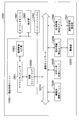
- FIG. 1 is a block diagram showing a functional configuration example of a solid-state imaging device 101A according to the first embodiment of the present technology.
- the solid-state imaging device 101A is, for example, a CMOS (Complementary Metal Oxide Semiconductor) image sensor.
- the solid-state imaging device 101A receives light from a subject, photoelectrically converts the light, and generates an image signal to capture an image.
- CMOS Complementary Metal Oxide Semiconductor
- the solid-state imaging device 101A includes, for example, a pixel array unit 111, a vertical drive unit 112, a column signal processing unit 113, a data storage unit 119, a horizontal drive unit 114, a system control unit 115, and a signal processing unit 118.
- the pixel array section 111 is formed on the semiconductor layer 11 (described later). Peripheral circuits such as the vertical drive unit 112, the column signal processing unit 113, the data storage unit 119, the horizontal drive unit 114, the system control unit 115, and the signal processing unit 118 are provided on the same semiconductor layer 11 as the pixel array unit 111, for example. It is formed.
- the pixel array unit 111 has a plurality of sensor pixels 110 including a photoelectric conversion unit 51 (described later) that generates and accumulates charges according to the amount of light incident from a subject. As shown in FIG. 1, the sensor pixels 110 are arranged in the horizontal direction (row direction) and the vertical direction (column direction). In the pixel array section 111, the pixel drive line 116 is wired along the row direction for each pixel row composed of the sensor pixels 110 arranged in one row in the row direction, and is composed of the sensor pixels 110 arranged in one column in the column direction. A vertical signal line (VSL) 117 is wired along the column direction for each pixel column.
- VSL vertical signal line
- the vertical drive unit 112 includes a shift register, an address decoder, and the like.
- the vertical driving unit 112 supplies signals or the like to the plurality of sensor pixels 110 via the plurality of pixel driving lines 116 to drive all of the plurality of sensor pixels 110 in the pixel array unit 111 at the same time, or Drive in rows.
- the vertical drive unit 112 has two scanning systems, for example, a reading scanning system and a sweeping scanning system.
- the read scanning system sequentially selects and scans the unit pixels of the pixel array unit 111 in units of rows in order to read signals from the unit pixels.
- the sweep-out scanning system performs the sweep-out scanning by a time corresponding to the shutter speed with respect to the read-out row in which the read-out scanning is performed by the read-out scanning system.
- the electronic shutter operation refers to an operation of discarding the photocharges of the photoelectric conversion unit 51 and newly starting the exposure, that is, newly starting the accumulation of the photocharges.
- the signal read by the read operation by the read scanning system corresponds to the amount of light incident after the read operation immediately before or the electronic shutter operation.
- the period from the read timing of the immediately preceding read operation or the sweep timing of the electronic shutter operation to the read timing of the current read operation is the photocharge accumulation time in the unit pixel, that is, the exposure time.
- a signal output from each unit pixel of the pixel row selectively scanned by the vertical drive unit 112 is supplied to the column signal processing unit 113 through each of the vertical signal lines 117.
- the column signal processing unit 113 performs, for each pixel column of the pixel array unit 111, predetermined signal processing on the signal output from each unit pixel of the selected row through the vertical signal line 117, and also performs the pixel signal after the signal processing. Is designed to be held temporarily.
- the column signal processing unit 113 includes, for example, a shift register and an address decoder, and performs noise removal processing, correlated double sampling processing, analog pixel signal A / D (Analog / Digital) conversion A / D conversion processing. Etc. to generate a digital pixel signal.
- the column signal processing unit 113 supplies the generated pixel signal to the signal processing unit 118.
- the horizontal drive unit 114 is composed of a shift register, an address decoder, and the like, and sequentially selects the unit circuits corresponding to the pixel columns of the column signal processing unit 113. By the selective scanning by the horizontal drive unit 114, the pixel signals processed by the column signal processing unit 113 for each unit circuit are sequentially output to the signal processing unit 118.
- the system control unit 115 includes a timing generator that generates various timing signals.
- the system control unit 115 controls the drive of the vertical drive unit 112, the column signal processing unit 113, and the horizontal drive unit 114 based on the timing signal generated by the timing generator.
- the signal processing unit 118 temporarily stores data in the data storage unit 119 as necessary, and performs signal processing such as arithmetic processing on the pixel signal supplied from the column signal processing unit 113 to obtain each pixel signal. Is output.
- the data storage unit 119 is adapted to temporarily store data necessary for the signal processing in the signal processing unit 118.
- the solid-state imaging device according to the present technology is not limited to the solid-state imaging device 101A illustrated in FIG. 1A, and may have a configuration such as the solid-state imaging device 101B illustrated in FIG. 1B or the solid-state imaging device 101C illustrated in FIG. 1C. May have.
- FIG. 1B is a block diagram illustrating a functional configuration example of a solid-state imaging device 101B as a first modification example according to the first embodiment of the present technology.
- FIG. 1C is a block diagram illustrating a functional configuration example of a solid-state imaging device 101C as a second modification example according to the first embodiment of the present technology.
- the data storage unit 119 is arranged between the column signal processing unit 113 and the horizontal driving unit 114, and the pixel signal output from the column signal processing unit 113 is stored in the data storage unit 119.
- the signal is supplied to the signal processing unit 118 via.
- the solid-state imaging device 101C in FIG. 1C has a data storage unit 119 and a signal processing unit 118 arranged in parallel between the column signal processing unit 113 and the horizontal driving unit 114.
- the column signal processing unit 113 is adapted to perform A / D conversion for converting an analog pixel signal into a digital pixel signal for each column of the pixel array unit 111 or for each plurality of columns of the pixel array unit 111. There is.
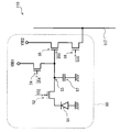
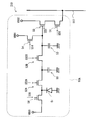
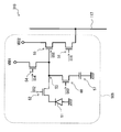
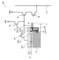
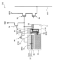
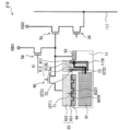
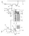
- FIG. 2 illustrates a circuit configuration example of the pixel circuit 50 in one sensor pixel 110 among the plurality of sensor pixels 110 that form the pixel array unit 111.
- the pixel circuit 50 includes a photoelectric conversion unit (PD) 51, a transfer transistor (TG) 52, a charge-voltage conversion unit (FD) 53, a reset transistor (RST) 54, and an amplification transistor (AMP) 55. , A selection transistor (SEL) 56 and a storage capacitor element (CP) 57.
- PD photoelectric conversion unit
- TG transfer transistor
- FD charge-voltage conversion unit
- RST reset transistor
- AMP amplification transistor
- SEL selection transistor
- CP storage capacitor element
- TG52, RST54, AMP55, and SEL56 are all N-type MOS transistors.
- Drive signals S52, S54, S55, and S56 are supplied to the respective gate electrodes of the TG 52, RST 54, AMP 55, and SEL 56 by the vertical drive unit 112 and the horizontal drive unit 114 based on the drive control of the system control unit 115, respectively.
- the drive signals S52, S54, S55, S56 are pulse signals in which a high level state is an active state (on state) and a low level state is an inactive state (off state).
- setting the drive signal to the active state is also referred to as turning on the drive signal
- setting the drive signal to the inactive state is also referred to as turning off the drive signal.
- the PD 51 is, for example, a photoelectric conversion element composed of a PN junction photodiode, and is configured to receive light from a subject and generate and accumulate charges according to the amount of received light by photoelectric conversion.
- the TG52 is connected between the PD51 and the FD53, and is configured to transfer the electric charge accumulated in the PD51 to the FD53 in accordance with the drive signal S52 applied to the gate electrode of the TG52.
- the TG 52 is a specific example corresponding to each of the “first transistor” and the “transfer transistor” of the present disclosure.
- RST54 has, for example, a drain connected to power supply VDD1 and a source connected to FD53.
- the RST 54 initializes, that is, resets the FD 53 according to the drive signal S54 applied to its gate electrode. For example, when the drive signal S54 is turned on and the RST 54 is turned on, the potential of the FD 53 is reset to the voltage level of the power supply VDD1. That is, the FD 53 is initialized.
- the FD 53 is a transfer destination of the charge generated in the PD 51, and is a floating diffusion region that converts the charge transferred from the PD 51 via the TG 52 into an electric signal (for example, a voltage signal) and outputs the electric signal.
- An RST 54 is connected to the FD 53, and a VSL 117 is connected via an AMP 55 and a SEL 56.
- the CP 57 is further connected to the FD 53 via a wiring W57 made of metal or the like (see FIGS. 3 and 4 described later).
- the CP 57 is a storage capacitor element that stores the charges generated in the PD 51 and transferred from the PD 51 together with the FD 53.
- the AMP 55 has, for example, a gate connected to the FD 53, a drain connected to the power supply VDD2, and a source connected to the SEL 56.
- the AMP 55 outputs an electric signal according to the potential of the FD 53.
- the SEL 56 has, for example, a drain connected to the AMP 55 and a source connected to the VSL 117. The SEL 56 is turned on when the sensor pixel 110 is selected, and outputs an electric signal from the FD 53 via the AMP 55 to the column signal processing unit 113 via the VSL 117.
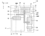
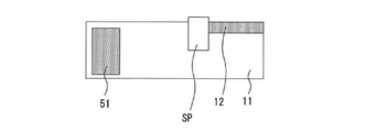
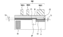
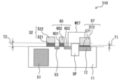
- FIG. 3 illustrates a planar configuration example of one sensor pixel 110 among the plurality of sensor pixels 110 configuring the pixel array section 111.
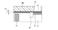
- FIG. 4 shows a cross-sectional configuration example of one sensor pixel 110, and corresponds to a cross section in the direction of the arrow along the IV-IV cutting line shown in FIG.
- the portion from the position P1 to the position P2 shows the YZ cross section along the Y-axis direction
- the portion from the position P2 to the position P3 shows the XZ cross section along the X-axis direction.
- the PD 51 occupies most of the area of the sensor pixel 110, and FD53, RST54, AMP55, SEL56, CP57, power supply VDD1, power supply VDD2 and VSL117 are provided in the peripheral area. It is provided.
- the TG 52 is provided at a position where it partially overlaps the PD 51 in the Z-axis direction (also referred to as the thickness direction or the depth direction).
- the sensor pixel 110 includes a semiconductor layer 11 formed of a semiconductor material such as Si (silicon), a PD 51 provided inside the semiconductor layer 11, and a semiconductor layer 11 on the semiconductor layer 11. And a TG 52 as a transfer unit provided in the.
- the TG 52 includes a laminated structure in which a gate insulating film 521 made of silicon oxide or the like and a gate electrode layer 522 are sequentially laminated on the semiconductor layer 11.
- the RST 54 includes a laminated structure in which a gate insulating film 541 made of silicon oxide or the like and a gate electrode layer 542 are sequentially laminated on the semiconductor layer 11.
- the FD 53 is provided between the TG 52 and the RST 54 in the uppermost part of the semiconductor layer 11.
- the CP 57 includes an insulating film 571 stacked on the impurity diffusion layer 12 provided on the uppermost part of the semiconductor layer 11 and a metal layer 572 stacked on the insulating film 571.
- the FD 53 is connected to the metal layer 572 of the CP 57 via the wiring W57.
- An element isolation part SP is provided between the RST 54 and the CP 57. Note that the description of the element isolation portion SP will be omitted below.
- the impurity diffusion layer 12 is provided with a contact layer 12T (see FIG. 3).
- the insulating film 571 of the CP 57 has the film thickness ET1 as the first electrical film thickness and the film thickness T1 as the first physical film thickness.
- both the gate insulating film 521 of the TG 52 and the gate insulating film 541 of the RST 54 have the film thickness ET2 as the second electrical film thickness and the film thickness T2 as the second physical film thickness.
- the film thickness ET2 is thicker than the film thickness ET1 (ET1 ⁇ ET2).
- the film thickness T2 is preferably thicker than the film thickness T1 (T1 ⁇ T2). That is, the insulating film 571 has a first withstand voltage, and the gate insulating films 521 and 541 have a second withstand voltage higher than the first withstand voltage.
- each gate insulating film in the AMP 55 and the SEL 56 has a film thickness ET2 larger than the film thickness ET1 and a film thickness T2 larger than the film thickness T1.
- the electric film thickness a parameter proportional to the physical thickness of the film divided by the dielectric constant of the film (physical thickness / dielectric constant), for example, an electrical capacitive in terms of SiO 2 EOT (Equivalent oxide thickness) representing a film thickness equivalent to is one specific example.
- SiO 2 EOT Equivalent oxide thickness
- the insulating film 571 of the CP 57, the gate insulating film 521 of the TG 52, and the gate insulating film 541 of the RST 54 may all be made of the same kind of material, that is, materials having the same dielectric constant.
- the dielectric constant of the insulating film 571 of the CP 57 is preferably higher than the dielectric constant of the gate insulating film 521 of the TG 52 or the gate insulating film 541 of the RST 54. This is because the storage capacity of the CP 57, that is, the saturated charge amount per area occupied by the unit pixel can be increased.
- the drive signal S52 to the TG 52 is turned on based on the drive control of the system control unit 115 when reading the electric charge generated and accumulated in the PD 51 that receives the light from the subject.
- the charge accumulated in the PD 51 is transferred from the PD 51 to the FD 53 via the TG 52.
- the FD 53 converts the electric signal into a level electric signal corresponding to each electric charge.
- the SEL 56 is turned on by the drive signal S56, the electric signal from the FD 53 is output to the column signal processing unit 113 through the VSL 117 via the AMP 55 and the SEL 56 in sequence.
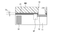
- FIGS. 5A to 5G are cross-sectional views showing one step in the method of manufacturing the solid-state imaging device 101A, and are cross-sectional views corresponding to FIG.
- the semiconductor layer 11 in which the PD 51 is embedded is prepared, and the impurity diffusion layer 12 is formed by ion implantation at a predetermined position of the uppermost layer of the semiconductor layer 11.
- an insulating material is deposited by, for example, a thermal oxidation method or a sputtering method so as to cover the semiconductor layer 11 over the entire surface to form an insulating film Z1.
- the insulating film Z1 is adjusted to have a predetermined thickness T2.
- a resist mask RM1 having an opening K1 at a position overlapping with a partial region of the impurity diffusion layer 12 is formed on the insulating film Z1.
- an opening Z1K is formed by selectively removing a portion of the insulating film Z1 that is not covered with the resist mask RM1, and a part of the impurity diffusion layer 12 is exposed.
- the insulating film Z2 is selectively formed so as to fill the opening Z1K.
- the insulating film Z2 is obtained by depositing an insulating material by, for example, a thermal oxidation method or a sputtering method. At that time, the insulating film Z2 is adjusted to have a predetermined thickness T1.
- the gate electrode material film M is formed so as to cover the insulating film Z1 and the insulating film Z2. Further, a resist mask RM2 that selectively covers the gate electrode material film M is formed.
- the resist mask RM2 includes portions RM2A to RM2C.
- the part RM2A is formed in a region where the TG 52 is to be formed
- the part RM2A is formed in a region where the RST 54 is to be formed
- the part RM2C is formed in a region where the CP 57 is to be formed.
- the resist mask RM2 is removed.
- a TG 52 in which a gate insulating film 521 and a gate electrode layer 522 were sequentially stacked, a gate insulating film 541 and a gate electrode layer 542 were sequentially stacked on the semiconductor layer 11.
- a CP 57 in which an insulating film 571 and a metal layer 572 are sequentially stacked on the RST 54 and the impurity diffusion layer 12 is obtained.
- the FD 53, the power supply VDD1 and the like are formed at predetermined positions on the uppermost layer of the semiconductor layer 11.
- AMP 55 and SEL 56 are not shown in FIGS. 5A to 5G, AMP 55 and SEL 56 may be formed simultaneously with formation of TG 52 and RST 54 by the same method as TG 52 and RST 54.
- the manufacturing of the solid-state imaging device 101A is completed by, for example, forming the wiring W57.
- the film thickness T2 of each transistor forming the pixel circuit 50 for example, the gate insulating film 521 of the TG 52 and the gate insulating film 541 of the RST 54 in each sensor pixel 110.
- the film thickness T1 (film thickness ET1) of the insulating film 571 of the CP 57 is made smaller than (film thickness ET2). Therefore, in the solid-state imaging device 101A, the saturated charge amount of the CP 57 in each sensor pixel 110 can be improved without increasing the area occupied by the CP 57. That is, in each sensor pixel 110, the saturated charge amount per unit area of the CP 57 becomes large. Therefore, in the solid-state imaging device 101A, for example, the area occupancy of the PD 51 in each sensor pixel 110 can be increased, and high integration of the sensor pixel 110 can be realized.
- the film thickness T2 (film thickness ET2) of the gate insulating film 521 of the TG 52 is made larger than the film thickness T1 (film thickness ET1) of the insulating film 571 of the CP57. Therefore, a higher voltage can be applied to the TG 52, and the charge can be transferred from the PD 51 to the FD 53 more quickly.
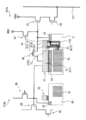
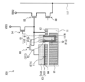
- FIG. 6 illustrates a circuit configuration example of the pixel circuit 50A in the sensor pixel 210 according to the second embodiment of the present technology.
- FIG. 7 illustrates a cross-sectional configuration example of the sensor pixel 210.
- the sensor pixel 210 is mounted on the solid-state imaging device 101A instead of the sensor pixel 110 according to the first embodiment, and realizes a so-called global shutter type image sensor.
- the global shutter method is a method of performing global exposure that basically starts exposure at the same time for all pixels and ends exposure at the same time for all pixels.
- all the pixels mean all the pixels of the part appearing in the image, and dummy pixels and the like are excluded.
- a method of moving the area to be globally exposed while performing global exposure in units of multiple rows (for example, several tens of rows) instead of simultaneously performing all pixels is also possible. It is included in the global shutter system.
- the global shutter system also includes a system in which global exposure is performed on pixels in a predetermined area, instead of all of the pixels in the image.
- the pixel circuit 50A is different from the pixel circuit 50 in that a charge holding unit (MEM) 59 is further provided between the PD 51 and the FD 53 instead of the CP 57. Further, the pixel circuit 50A is different from the pixel circuit 50 in that it has a first transfer transistor (TG) 52A and a second transfer transistor (TG) 52B instead of the TG 52.
- the TG 52A is arranged between the PD 51 and the MEM 59
- the TG 52B is arranged between the MEM 59 and the FD 53.
- the pixel circuit 50A further has a power supply VDD3 as a transfer destination of charges generated in the PD 51, and also has a discharge transistor (OFG) 58 between the PD 51 and the power supply VDD3. Except for these points, the pixel circuit 50A has substantially the same configuration as the pixel circuit 50 according to the above-described first embodiment.
- the power supply VDD3, the impurity diffusion layer 12, the FD 53, the power supply VDD1 and the like are formed in the uppermost layer of the semiconductor layer 11.
- OFG58, TG52A, MEM59, TG52B, RST54, etc. are formed on the semiconductor layer 11.
- the OFG 58 has a drain connected to the power supply VDD3 and a source connected to a wiring connecting the TG 52 and the PD 51.
- the OFG 58 includes a stacked structure in which a gate insulating film 581 made of silicon oxide or the like and a gate electrode layer 582 are sequentially stacked on the semiconductor layer 11.
- the OFG 58 initializes, that is, resets the PD 51 according to the drive signal S58 applied to the gate electrode layer 582. Resetting the PD 51 means depleting the PD 51.
- the OFG 58 forms an overflow path between the TG 52 and the power supply VDD3, and discharges the electric charge overflowing from the PD 51 to the power supply VDD3.
- the FD holding type global shutter in which the OFG 58 can directly reset the PD 51 can be realized.
- the MEM 59 is provided between the PD 51 and the FD 53, and in order to realize the global shutter function, a region that temporarily holds the electric charge generated and accumulated in the PD 51 until it is transferred to the FD 53. Is.
- the MEM 59 includes a stacked structure in which an insulating film 591 made of silicon oxide or the like and a gate electrode layer 592 made of polysilicon or the like are sequentially stacked on the semiconductor layer 11.
- the TG52A is arranged between PD51 and MEM59, and TG52B is arranged between MEM59 and FD53.
- the TG 52A includes a stacked structure in which a gate insulating film 521A made of silicon oxide or the like and a gate electrode layer 522A are sequentially stacked on the semiconductor layer 11.
- the TG 52A is configured to transfer the charge accumulated in the PD 51 to the MEM 59 according to the drive signal S52A applied to the gate electrode layer 522A.
- the TG 52B includes a stacked structure in which a gate insulating film 521B made of silicon oxide or the like and a gate electrode layer 522B are sequentially stacked on the semiconductor layer 11.
- the TG 52B is configured to transfer the charge temporarily held in the MEM 59 to the FD 53 according to the drive signal S52B applied to the gate electrode layer 522B.
- the drive signal S52A is turned off
- the TG52A is turned off
- the drive signal S52B is turned on
- the TG52B is turned on
- the electric charge held in the MEM 59 is transferred to the FD 53 via the TG 52B. It has become.
- the insulating film 591 of the MEM 59 has the film thickness ET1 as the first electrical film thickness and the film thickness T1 as the first physical film thickness.
- the insulating film 591 is a specific example corresponding to the “first insulating film” of the present disclosure.
- the gate insulating film 581 of the OFG 58, the gate insulating film 521A of the TG 52A, the gate insulating film 521B of the TG 52B, and the gate insulating film 541 of the RST 54 all have the film thickness ET2 as the second electrical film thickness.
- the film thickness ET2 is thicker than the film thickness ET1 (ET1 ⁇ ET2).
- the film thickness T2 is thicker than the film thickness T1 (T1 ⁇ T2).
- the gate insulating films 581, 521A, 521B, 541 are one specific example corresponding to the “second insulating film” of the present disclosure.
- Each gate insulating film in the AMP 55 and the SEL 56 has a film thickness ET2 thicker than the film thickness ET1 and a film thickness T2 thicker than the film thickness T1.
- the insulating film 591 and the gate insulating films 581, 521A, 521B, 541 of the MEM 59 may be made of the same material, that is, a material having the same dielectric constant.
- the dielectric constant of the insulating film 591 of the MEM 59 is preferably higher than that of each of the gate insulating films 581, 521A, 521B, and 541. This is because the storage capacity of the MEM 59, that is, the saturated charge amount per area occupied by the unit pixel can be increased.
- the electric charge from the PD 51 is transferred to the MEM 59, and a memory holding type global shutter can be realized.
- the drive signal S52A applied to the gate electrode of the TG 52A is turned on and the TG 52A is turned on, the charge accumulated in the PD 51 is transferred to the MEM 59 via the TG 52A.
- Is becoming The MEM 59 is an area for temporarily holding the electric charge accumulated in the PD 51 in order to realize the global shutter function.
- the TG 52B is configured to transfer the electric charge held in the MEM 59 to the FD 53 according to the drive signal S52B applied to the gate electrode layer 522B of the TG 52B. For example, when the drive signal S52 is turned off, the TG52A is turned off, the drive signal S52B is turned on, and the TG52B is turned on, the electric charge held in the MEM 59 is transferred to the FD 53 via the TG 52B.
- the sensor pixel 210 can improve the saturated charge amount of the MEM 59 without increasing the area occupied by the MEM 59. That is, the saturation charge amount per unit area of the MEM 59 becomes large in each sensor pixel 210. Therefore, in the global shutter type solid-state imaging device including a plurality of the sensor pixels 210, high integration of the sensor pixels 210 can be realized.
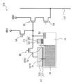
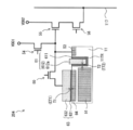
- FIG. 8 illustrates a circuit configuration example of the pixel circuit 50B in the sensor pixel 310 according to the third embodiment of the present technology.
- FIG. 9 illustrates a cross-sectional configuration example of the sensor pixel 310.
- the sensor pixel 310 further includes a switching transistor (FDG) 60 provided between the FD 53 and the CP 57 in addition to the sensor pixel 110 according to the first embodiment. Except for that point, the sensor pixel 310 has substantially the same configuration as the sensor pixel 110.
- the FDG 60 includes, for example, an impurity diffusion layer 603 provided on the uppermost layer of the semiconductor layer 11, a gate insulating film 601 stacked on the semiconductor layer 11, and a gate insulating film 601 on the gate insulating film 601. And a gate electrode layer 602 that is stacked over the gate electrode layer 602.
- the drive signal S60 is supplied to the gate electrode layer 602 by the vertical drive unit 112 and the horizontal drive unit 114 under the drive control of the system control unit 115.
- the FD 53 and the CP 57 are connected.
- the electrical film thickness of the gate insulating film 601 is substantially the same as the film thickness ET2 of the gate insulating film 521 of the TG 52, for example, and is thicker than the film thickness ET1 of the insulating film 571 of the CP 57.
- the physical thickness of the gate insulating film 601 is substantially the same as the film thickness T2 of the gate insulating film 521 of the TG 52, for example. And is thicker than the film thickness T1 of the insulating film 571 of the CP 57.
- the film thickness T1 (film thickness ET1) of the insulating film 571 of the CP 57 is set to the gate insulating film of each transistor forming the pixel circuit 50B, for example, the gate insulating film of TG52. 521 and the gate insulating film 601 of the FDG 60 are made thinner than the film thickness T2 (film thickness ET2). Therefore, the same effect as the sensor pixel 110 according to the first embodiment can be expected.
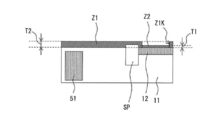
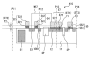
- FIG. 10 shows a planar configuration example of the sensor pixel 410 according to the second embodiment of the present technology.
- FIG. 11 shows a cross-sectional configuration example of the sensor pixel 410, and corresponds to the cross section in the direction of the arrow along the XI-XI cutting line shown in FIG.
- the part from position P11 to position P12 and the part from position P13 to position P14 each show a YZ cross section along the Y-axis direction
- the part from position P12 to position P13 is the X-axis.
- the XZ cross section along the direction is shown.
- the AMP 55 includes a laminated structure in which a gate insulating film 551 made of silicon oxide or the like and a gate electrode layer 552 are sequentially laminated on the semiconductor layer 11.
- the gate insulating film in the AMP 55 has a film thickness T2 (film thickness ET2) larger than the film thickness T1 (film thickness ET1), for example.
- the gate insulating film 551 in the AMP 55 has, for example, the film thickness ET3 as the third electrical film thickness and the film thickness as the third physical film thickness. Having T3.
- the film thickness ET3 of the gate insulating film 551 is thinner than the film thickness ET2 of the gate insulating film 521 of the TG 52, for example. Further, for example, when the respective constituent materials of the gate insulating film 551 and the gate insulating film 521 are the same, that is, when the gate insulating film 551 and the gate insulating film 521 are both made of the material having the same dielectric constant, the gate insulating film 551 Has a thickness T3 smaller than the thickness T2 of the gate insulating film 521.
- FIG. 11 illustrates the case where the film thickness T3 (film thickness ET3) is substantially the same as the film thickness T1 (film thickness ET1), the film thickness T3 (film thickness ET3) is the film thickness T1. It may be different from (film thickness ET1).
- the AMP 55 is one specific example corresponding to the “second transistor” of the present invention
- the gate insulating film 551 is one specific example corresponding to the “third insulating film” of the present disclosure.
- the film thickness T1 (film thickness ET1) of the insulating film 571 of the CP 57 is set to the gate insulating film of each transistor forming the sensor pixel 410, for example, the gate insulating film of TG52. It is made thinner than the film thickness T2 (film thickness ET2) in 521. Therefore, the same effect as the sensor pixel 110 according to the first embodiment can be expected.
- the thickness T3 (thickness ET3) of the gate insulating film 551 in the AMP 55 is equal to the thickness ET2 (thickness ET2 of the gate insulating film 521 of the TG 52 and the gate insulating film 601 of the FDG 60). ) Is thinner than. Therefore, RTS noise (random telegraph signal noise) in the AMP 55 can be reduced.
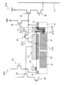
- FIG. 12 shows an example of the overall configuration of a sensor pixel 510 according to the fifth embodiment of the present technology.
- the storage capacitor element (CP) 57 is stacked at a position overlapping the photoelectric conversion unit (PD) 51 in the thickness direction of the semiconductor layer 11.
- CP57 is a MOS capacitor connected to the FDG 60. Except for this point, the sensor pixel 510 has substantially the same configuration as the sensor pixel 310 according to the above-described third embodiment.
- the sensor pixel 510 can switch between low conversion efficiency and high conversion efficiency according to the illuminance of the subject. That is, the capacity of the FD 53 can be switched by the on / off operation of the FDG 60. For example, by turning on the FDG 60, the FD 53 is connected to the CP 57 which is a MOS capacitor. As a result, the capacity of the FD 53 increases and the conversion efficiency decreases.
- the film thickness T1 (film thickness ET1) of the insulating film 571 of the CP 57 is set to the gate insulating film of each transistor forming the sensor pixel 510, for example, the gate insulating film of TG52. 521 and the gate insulating film 601 of the FDG 60 are made thinner than the film thickness T2 (film thickness ET2). Therefore, the same effect as the sensor pixel 110 according to the first embodiment can be expected.
- the CP 57 is laminated on the PD 51, so that the ratio of the formation area of the PD 51 to the area occupied by the sensor pixel 510 can be increased. Therefore, it is advantageous for high integration of the solid-state imaging device.
- FIG. 13 shows an overall configuration example of the sensor pixel 610 according to the sixth embodiment of the present technology.
- the TG 61 is provided instead of the TG 52.
- the TG 61 is a vertical transistor having a gate insulating film 611 and a gate electrode 612 including a plug 612a extending in the thickness direction of the semiconductor layer 11.
- the plug 612a is inserted in a trench 11TR formed in the semiconductor layer 11 and extending in the thickness direction of the semiconductor layer 11.
- a head 612b is provided on the upper end of the plug 612a.
- Gate electrode 612 is separated from semiconductor layer 11 by gate insulating film 611 covering the inner surface of trench 11TR.
- Trench 11TR has a wall surface and a bottom surface which are entirely covered with gate insulating film 611. Except for this point, the sensor pixel 610 has substantially the same configuration as the sensor pixel 510 according to the fifth embodiment described above.
- the TG 61 is a specific example corresponding to the “first transistor” and the “vertical transistor” of the present disclosure.
- the gate insulating film 611 is a specific example corresponding to the “second insulating film” of the present disclosure.
- the minimum value of the film thickness ET1 which is the electric film thickness of the insulating film 571 of the CP 57 is smaller than the minimum value of the film thickness ET2 which is the electric film thickness of the gate insulating film 611. Therefore, for example, when the dielectric constant of the insulating film 571 and the dielectric constant of the gate insulating film 611 are the same, the minimum value of the film thickness T1 which is the physical film thickness of the insulating film 571 of CP57 is the same as that of the gate insulating film 611. The thickness is smaller than the minimum value of the physical thickness T2. Therefore, the same effect as the sensor pixel 110 according to the first embodiment can be expected.
- the vertical transistor TG61 is provided in the sensor pixel 610. Therefore, the plug 612a of the TG 61 can be brought closer to the PD 51. Therefore, it becomes easier to transfer the charges from the PD 51 to the FD 53.
- FIG. 14 shows an overall configuration example of the sensor pixel 710 according to the seventh embodiment of the present technology.
- the sensor pixel 710 further includes, for example, an n + region 64 between the PD 51 and the CP 57. That is, the CP 57 is a plane type n-type MOS capacitor. Except for this point, the sensor pixel 710 has substantially the same configuration as the sensor pixel 610 according to the sixth embodiment described above.
- the minimum value of the film thickness ET1 which is the electric film thickness of the insulating film 571 of the CP 57 is smaller than the minimum value of the film thickness ET2 which is the electric film thickness of the gate insulating film 611. Therefore, for example, when the dielectric constant of the insulating film 571 and the dielectric constant of the gate insulating film 611 are the same, the minimum value of the film thickness T1 which is the physical film thickness of the insulating film 571 of CP57 is the same as that of the gate insulating film 611. The thickness is smaller than the minimum value of the physical thickness T2. Therefore, the same effect as the sensor pixel 110 according to the first embodiment can be expected.
- FIG. 15 shows an example of the overall configuration of a sensor pixel 810 according to the eighth embodiment of the present technology.
- the sensor pixel 810 includes a storage capacitor element (CP) 63 having an insulating film 631 and a conductive layer 632 instead of the CP 57.
- CP storage capacitor element
- a plurality of trenches 64TR are formed in the n + region 64, and the insulating film 631 of CP63 is provided so as to cover the inner surface thereof.
- the conductive layer 632 of CP63 includes a protrusion 632T inserted into the plurality of trenches 64TR. That is, CP63 is a trench type MOS capacitor including an uneven structure.
- the sensor pixel 810 has substantially the same configuration as the sensor pixel 710 according to the seventh embodiment except for these points.
- the minimum value of the film thickness ET1 which is the electrical film thickness of the insulating film 631 of the CP 63 is smaller than the minimum value of the film thickness ET2 which is the electrical film thickness of the gate insulating film 611. Therefore, for example, when the dielectric constant of the insulating film 631 and the dielectric constant of the gate insulating film 611 are the same, the minimum value of the film thickness T1 which is the physical film thickness of the insulating film 631 of CP63 is the minimum value of the gate insulating film 611. The thickness is smaller than the minimum value of the physical thickness T2. Therefore, the same effect as the sensor pixel 110 according to the first embodiment can be expected.
- CP63 including a concavo-convex structure is provided instead of CP57, and the surface area of the insulating film 631 is made larger than the surface area of the insulating film 571. Therefore, the capacitance of CP63 is larger than that of CP57. Can be increased.
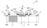
- FIG. 16A shows a configuration example of a main part of a solid-state imaging device according to the ninth embodiment of the present technology.
- the solid-state imaging device according to the present embodiment has sensor pixels 910a and sensor pixels 910b arranged so as to be adjacent to each other.
- the sensor pixel 910a has substantially the same configuration as the sensor pixel 710 of the seventh embodiment shown in FIG.
- the sensor pixel 910b is provided in the semiconductor layer 80 adjacent to the semiconductor layer 11, and has a photoelectric conversion unit (PD) 81, a transfer transistor (TG) 82, a charge-voltage conversion unit (FD) 83, a reset transistor (RST) 84, and an amplification.
- PD photoelectric conversion unit
- TG transfer transistor
- FD charge-voltage conversion unit
- RST reset transistor
- PD81, TG82, FD83, RST84, AMP85, and SEL86 have the functions corresponding to PD51, TG52, FD53, RST54, AMP55, and SEL56, respectively. That is, for example, the PD 81 in the sensor pixel 910b is configured to generate electric charge according to the amount of received light by photoelectric conversion, like the PD 51.
- the sensor pixel 910b does not include a storage capacitor element unlike the sensor pixel 910a. Therefore, the CP 57 in the sensor pixel 910a stores not only the charge generated by the PD 51 but also the charge generated by the PD 81.
- the sensitivity of the PD 51 of the sensor pixel 910a is higher than the sensitivity of the PD 81 of the adjacent sensor pixel 910b. That is, the light receiving area of the PD 51 in the sensor pixel 910a is larger than the light receiving area of the PD 81 in the sensor pixel 910b. Therefore, in the solid-state imaging device according to the present embodiment, the sensor pixel 910a including the CP 57 is used as a high sensitivity pixel, and the sensor pixel 910b is used as a low sensitivity pixel, whereby the dynamic range can be expanded.
- the sensor pixel 910b is provided in the semiconductor layer 80 different from the semiconductor layer 11 in the solid-state imaging device shown in FIG. 16A, the sensor pixel 910b may be provided in the same semiconductor layer 11 as the sensor pixel 910a. ..
- the sensor pixel 910a and the sensor pixel 910b share the CP 57.
- the present disclosure is not limited to this.
- the CP 57 does not have to be shared by the sensor pixel 910a and the sensor pixel 910b.
- the FD 53 of the sensor pixel 910a is not connected to the CP 57 of the sensor pixel 910a, but the FD 83 of the sensor pixel 910b is connected.
- the charge generated by the PD 51 of the sensor pixel 910a is not stored in the CP 57, and the charge generated by the PD 81 of the sensor pixel 910b is stored in the CP 57.
- FIG. 17 illustrates a configuration example of a main part of a solid-state imaging device according to the tenth embodiment of the present technology.
- the solid-state imaging device according to the present embodiment includes sensor pixels 910a and sensor pixels 910b arranged adjacent to each other, as in the solid-state imaging device according to the ninth embodiment.
- the sensor pixel 910b is provided in the same semiconductor layer 11 as the sensor pixel 910a.
- CP57 is arranged so as to straddle both PD51 and PD81 in the in-plane direction of semiconductor layer 11, that is, part of CP57 is PD51 and PD81 in the thickness direction of semiconductor layer 11. Is provided in a position overlapping with both. Except for these points, the solid-state imaging device (FIG. 17) of the present embodiment has substantially the same configuration as the solid-state imaging device (FIG. 16) of the ninth embodiment except for these points.
- FIG. 18 is a block diagram showing a configuration example of a camera 2000 as an electronic device to which the present technology is applied.
- the camera 2000 is an optical unit 2001 including a lens group, an imaging device (imaging device) 2002 to which the above-described solid-state imaging device 101 and the like (hereinafter, solid-state imaging device 101 and the like) is applied, and a camera signal processing circuit.
- a DSP (Digital Signal Processor) circuit 2003 is provided.
- the camera 2000 also includes a frame memory 2004, a display unit 2005, a recording unit 2006, an operation unit 2007, and a power supply unit 2008.
- the DSP circuit 2003, the frame memory 2004, the display unit 2005, the recording unit 2006, the operation unit 2007, and the power supply unit 2008 are connected to each other via a bus line 2009.
- the optical unit 2001 captures incident light (image light) from a subject and forms an image on the imaging surface of the imaging device 2002.
- the imaging device 2002 converts the light amount of the incident light imaged on the imaging surface by the optical unit 2001 into an electric signal on a pixel-by-pixel basis and outputs the electric signal as a pixel signal.
- the display unit 2005 includes a panel type display device such as a liquid crystal panel or an organic EL panel, and displays a moving image or a still image captured by the image capturing device 2002.
- the recording unit 2006 records a moving image or a still image captured by the image capturing apparatus 2002 on a recording medium such as a hard disk or a semiconductor memory.
- the operation unit 2007 issues operation commands for various functions of the camera 2000 under the operation of the user.
- the power supply unit 2008 appropriately supplies various power supplies serving as operating power supplies of the DSP circuit 2003, the frame memory 2004, the display unit 2005, the recording unit 2006, and the operation unit 2007 to these supply targets.
- the technology according to the present disclosure (this technology) can be applied to various products.
- the technology according to the present disclosure is realized as a device mounted on any type of moving body such as an automobile, an electric vehicle, a hybrid electric vehicle, a motorcycle, a bicycle, personal mobility, an airplane, a drone, a ship, and a robot. May be.
- FIG. 19 is a block diagram showing a schematic configuration example of a vehicle control system which is an example of a mobile body control system to which the technology according to the present disclosure can be applied.
- the vehicle control system 12000 includes a plurality of electronic control units connected via a communication network 12001.
- the vehicle control system 12000 includes a drive system control unit 12010, a body system control unit 12020, a vehicle exterior information detection unit 12030, a vehicle interior information detection unit 12040, and an integrated control unit 12050.
- a microcomputer 12051, a voice image output unit 12052, and an in-vehicle network I / F (Interface) 12053 are shown as a functional configuration of the integrated control unit 12050.
- the drive system control unit 12010 controls the operation of devices related to the drive system of the vehicle according to various programs.
- the drive system control unit 12010 includes a drive force generation device for generating a drive force of a vehicle such as an internal combustion engine or a drive motor, a drive force transmission mechanism for transmitting the drive force to wheels, and a steering angle of the vehicle. It functions as a steering mechanism for adjusting and a control device such as a braking device for generating a braking force of the vehicle.
- the body system control unit 12020 controls the operation of various devices mounted on the vehicle body according to various programs.
- the body system control unit 12020 functions as a keyless entry system, a smart key system, a power window device, or a control device for various lamps such as a head lamp, a back lamp, a brake lamp, a winker, or a fog lamp.
- the body system control unit 12020 can be input with radio waves or signals of various switches transmitted from a portable device that substitutes for a key.
- the body system control unit 12020 receives input of these radio waves or signals and controls the vehicle door lock device, power window device, lamp, and the like.
- the vehicle exterior information detection unit 12030 detects information outside the vehicle equipped with the vehicle control system 12000.
- the image pickup unit 12031 is connected to the vehicle exterior information detection unit 12030.
- the vehicle exterior information detection unit 12030 causes the image capturing unit 12031 to capture an image of the vehicle exterior and receives the captured image.
- the vehicle exterior information detection unit 12030 may perform object detection processing or distance detection processing such as people, vehicles, obstacles, signs, or characters on the road surface based on the received image.
- the image pickup unit 12031 is an optical sensor that receives light and outputs an electric signal according to the amount of received light.
- the image pickup unit 12031 can output the electric signal as an image or as distance measurement information.
- the light received by the imaging unit 12031 may be visible light or invisible light such as infrared light.
- the in-vehicle information detection unit 12040 detects in-vehicle information.
- a driver state detection unit 12041 that detects the state of the driver is connected.
- the driver state detection unit 12041 includes, for example, a camera that images the driver, and the in-vehicle information detection unit 12040 determines the degree of fatigue or concentration of the driver based on the detection information input from the driver state detection unit 12041. It may be calculated or it may be determined whether or not the driver is asleep.
- the microcomputer 12051 calculates the control target value of the driving force generation device, the steering mechanism or the braking device based on the information on the inside and outside of the vehicle acquired by the outside information detection unit 12030 or the inside information detection unit 12040, and the drive system control unit.
- a control command can be output to 12010.
- the microcomputer 12051 realizes functions of ADAS (Advanced Driver Assistance System) including avoidance or impact mitigation of vehicle collision, follow-up traveling based on inter-vehicle distance, vehicle speed maintenance traveling, vehicle collision warning, vehicle lane departure warning, and the like. It is possible to perform cooperative control for the purpose.
- ADAS Advanced Driver Assistance System
- the microcomputer 12051 controls the driving force generation device, the steering mechanism, the braking device, or the like on the basis of the information around the vehicle acquired by the vehicle exterior information detection unit 12030 or the vehicle interior information detection unit 12040, so that the driver's It is possible to perform cooperative control for the purpose of autonomous driving or the like that autonomously travels without depending on the operation.
- the microcomputer 12051 can output a control command to the body system control unit 12020 based on the information outside the vehicle acquired by the outside information detection unit 12030.
- the microcomputer 12051 controls the headlamp according to the position of the preceding vehicle or the oncoming vehicle detected by the vehicle exterior information detection unit 12030, and performs cooperative control for the purpose of antiglare such as switching the high beam to the low beam. It can be carried out.
- the voice image output unit 12052 transmits an output signal of at least one of a voice and an image to an output device capable of visually or audibly notifying information to a passenger of the vehicle or the outside of the vehicle.
- an audio speaker 12061, a display unit 12062, and an instrument panel 12063 are illustrated as output devices.
- the display unit 12062 may include at least one of an on-board display and a head-up display, for example.
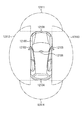
- FIG. 20 is a diagram showing an example of the installation position of the imaging unit 12031.
- the imaging unit 12031 includes imaging units 12101, 12102, 12103, 12104, and 12105.
- the image capturing units 12101, 12102, 12103, 12104, and 12105 are provided at positions such as the front nose of the vehicle 12100, the side mirrors, the rear bumper, the back door, and the upper part of the windshield inside the vehicle.
- the image capturing unit 12101 provided on the front nose and the image capturing unit 12105 provided on the upper part of the windshield in the vehicle interior mainly acquire an image in front of the vehicle 12100.
- the image capturing units 12102 and 12103 provided in the side mirrors mainly acquire images of the side of the vehicle 12100.
- the image capturing unit 12104 provided in the rear bumper or the back door mainly acquires an image behind the vehicle 12100.
- the imaging unit 12105 provided on the upper part of the windshield inside the vehicle is mainly used for detecting a preceding vehicle, a pedestrian, an obstacle, a traffic signal, a traffic sign, a lane, or the like.
- FIG. 20 shows an example of the shooting range of the imaging units 12101 to 12104.
- the imaging range 12111 indicates the imaging range of the imaging unit 12101 provided on the front nose
- the imaging ranges 12112 and 12113 indicate the imaging ranges of the imaging units 12102 and 12103 provided on the side mirrors
- the imaging range 12114 indicates The imaging range of the imaging part 12104 provided in a rear bumper or a back door is shown. For example, by overlaying the image data captured by the image capturing units 12101 to 12104, a bird's-eye view image of the vehicle 12100 viewed from above can be obtained.
- At least one of the imaging units 12101 to 12104 may have a function of acquiring distance information.
- at least one of the image capturing units 12101 to 12104 may be a stereo camera including a plurality of image capturing elements or may be an image capturing element having pixels for phase difference detection.
- the microcomputer 12051 based on the distance information obtained from the imaging units 12101 to 12104, the distance to each three-dimensional object in the imaging range 12111 to 12114 and the temporal change of this distance (relative speed with respect to the vehicle 12100).
- the closest three-dimensional object on the traveling path of the vehicle 12100 which is traveling in the substantially same direction as the vehicle 12100 at a predetermined speed (for example, 0 km / h or more), can be extracted as a preceding vehicle. it can.
- the microcomputer 12051 can set an inter-vehicle distance to be secured in front of the preceding vehicle in advance, and can perform automatic braking control (including follow-up stop control), automatic acceleration control (including follow-up start control), and the like. In this way, it is possible to perform cooperative control for the purpose of autonomous driving, which autonomously travels without depending on the operation of the driver.
- the microcomputer 12051 uses the distance information obtained from the image capturing units 12101 to 12104 to convert three-dimensional object data regarding a three-dimensional object to other three-dimensional objects such as two-wheeled vehicles, ordinary vehicles, large vehicles, pedestrians, telephone poles, and the like. It can be classified, extracted, and used for automatic avoidance of obstacles. For example, the microcomputer 12051 distinguishes obstacles around the vehicle 12100 into obstacles visible to the driver of the vehicle 12100 and obstacles difficult to see. Then, the microcomputer 12051 determines the collision risk indicating the risk of collision with each obstacle, and when the collision risk is equal to or more than the set value and there is a possibility of collision, the microcomputer 12051 outputs the audio through the audio speaker 12061 and the display unit 12062. A driver can be assisted for avoiding a collision by outputting an alarm to the driver and performing forced deceleration or avoidance steering through the drive system control unit 12010.
- At least one of the image capturing units 12101 to 12104 may be an infrared camera that detects infrared rays.
- the microcomputer 12051 can recognize a pedestrian by determining whether or not the pedestrian is present in the images captured by the imaging units 12101 to 12104. To recognize such a pedestrian, for example, a procedure for extracting a feature point in an image captured by the image capturing units 12101 to 12104 as an infrared camera and pattern matching processing on a series of feature points indicating the contour of an object are performed to determine whether or not the pedestrian is a pedestrian.
- the voice image output unit 12052 causes the recognized pedestrian to have a rectangular contour line for emphasis.
- the display unit 12062 is controlled so as to superimpose. Further, the audio image output unit 12052 may control the display unit 12062 to display an icon indicating a pedestrian or the like at a desired position.
- the technology according to the present disclosure can be applied to the imaging unit 12031 among the configurations described above.
- the solid-state imaging device 101A or the like shown in FIG. 1 or the like can be applied to the imaging unit 12031.
- the present disclosure has been described above with reference to some embodiments and modifications, the present disclosure is not limited to the above embodiments and the like, and various modifications are possible.
- the solid-state imaging device of the present disclosure is not limited to those having the pixel circuits described in the above embodiments and the like, and includes those having various pixel circuits.
- FIG. 21A is a cross-sectional view illustrating a configuration example of a main part of a solid-state imaging device 201 as a third modification example of the present disclosure.
- FIG. 21B is a circuit diagram of the solid-state imaging device 201.
- the solid-state imaging device 201 has two sensor pixels PX1 and PX2 arranged so as to be adjacent to each other.
- the sensor pixel PX1 includes a photoelectric conversion unit PD1 embedded in the semiconductor layer 200, a transfer gate TGL provided near the surface 200A of the semiconductor layer 200, a charge / voltage conversion unit FD1, a charge / voltage conversion gate FDG, a reset transistor RST1, It includes an amplification transistor AMP, a selection transistor SEL56 and a floating capacitor FC.
- the sensor pixel PX2 includes a photoelectric conversion unit PD2 embedded in the semiconductor layer 200, a transfer gate TGS and a floating capacitor gate FCG provided near the surface 200A of the semiconductor layer 200.
- the first end of the floating capacitor FC is connected to the power source FCVDD in the sensor pixel PX1
- the second end of the floating capacitor FC is connected to the intermediate portion of the transfer gate TGS and the floating capacitor gate FCG in the sensor pixel PX2.
- the color filter CF1 and the on-chip lens LN1 are sequentially stacked on the back surface 200B of the semiconductor layer 200.
- the color filter CF2 and the on-chip lens LN2 are sequentially stacked on the back surface 200B of the semiconductor layer 200.
- a light shielding film BM is selectively embedded in the color filters CF1 and CF2.
- the light shielding film BM is provided at the boundary between adjacent sensor pixels.
- a light shielding wall BW extending in the thickness direction of the semiconductor layer 200 is provided.
- the light-shielding film BM and the light-shielding wall BW are made of, for example, metal, but are not limited thereto.
- the photoelectric conversion unit PD1 and the floating capacitor FC are stacked so as to overlap each other in the thickness direction of the semiconductor layer 200.
- the transfer gate TGL is a vertical gate extending in the thickness direction of the semiconductor layer 200 up to the photoelectric conversion unit PD1.
- the light shielding film BM is embedded in the color filters CF1 and CF2, but the present disclosure is not limited to this.
- a layer including the color filters CF1 and CF2 may be provided separately from the layer including the light shielding film BM.
- the plug of the gate electrode of the vertical transistor is provided at a position different from the photoelectric conversion unit in plan view, but the present disclosure is not limited to this.
- the gate electrode of the vertical transistor includes the plug and the cap that covers the upper end of the plug, but the present disclosure is not limited thereto. That is, the present disclosure also includes the respective forms shown in FIGS. 23 to 25.
- the plug 612a of the gate electrode 612 of the TG 61 which is a vertical transistor, is positioned so as to overlap the PD 51 in plan view.
- the plug 612a may be inserted into the PD 51.
- the gate electrode 612 of the vertical transistor TG61 does not have the head 612b and has only the plug 612a. May be.
- the gate electrode 612 of the TG 61 that is a vertical transistor does not have the head 612b and has only the plug 612a,
- the plug 612a may be inserted into the PD 51.
- the imaging device of the present disclosure is not limited to the imaging device that detects the light amount distribution of visible light and acquires it as an image, and acquires the distribution of the incident amount of infrared rays, X-rays, particles or the like as an image. It may be an imaging device.
- the solid-state imaging device and the electronic device according to the embodiment of the present disclosure are suitable for high integration of pixels.
- the effect of the present disclosure is not limited to this, and may be any of the effects described below.
- the present technology may have the following configurations. (1) A semiconductor layer, A photoelectric conversion unit which is provided in the semiconductor layer and which generates charges according to the amount of received light by photoelectric conversion, A storage capacitor provided in the semiconductor layer and including a first insulating film having a first electrical thickness; A solid-state imaging device comprising: a first transistor provided in the semiconductor layer, the first transistor including a second insulating film having a second electrical thickness that is thicker than the first electrical thickness.
- the solid-state imaging device according to (1) further including a second transistor including a third insulating film having a third electric film thickness smaller than the second electric film thickness.
- the second transistor is an amplification transistor
- the third insulating film is a gate insulating film of the amplification transistor.
- the storage capacitor element is stacked at a position overlapping the photoelectric conversion unit in a thickness direction of the semiconductor layer.
- the first transistor is a vertical transistor including a gate electrode extending in the thickness direction of the semiconductor layer as a second conductive layer
- the thinnest physical film thickness of the second insulating film is thicker than the thickest physical film thickness of the first insulating film.
- the gate electrode of the vertical transistor has a plug inserted into a trench formed in the semiconductor layer and extending in a thickness direction, The solid-state imaging device according to (5) or (6), wherein the trench has a wall surface and a bottom surface which are entirely covered with the second insulating film.
- the storage capacitor element is a MOS capacitor.
- the solid-state imaging device according to any one of (1) to (7) above.
- the storage capacitor element stores the electric charge generated by the photoelectric conversion unit.
- the adjacent pixel has an adjacent photoelectric conversion unit that generates a charge according to the amount of received light by photoelectric conversion
- the storage capacitor element is provided so as to extend over both the photoelectric conversion section and the adjacent photoelectric conversion section in the in-plane direction of the semiconductor layer.
- the solid-state imaging device according to (12) or (13) above, wherein the sensitivity of the photoelectric conversion unit is higher than the sensitivity of the adjacent photoelectric conversion unit.
- 15) Further comprising an adjacent pixel provided in the semiconductor layer so as to be adjacent to a pixel including the photoelectric conversion unit and the storage capacitor element, The adjacent pixel has an adjacent photoelectric conversion unit that generates a charge according to the amount of received light by photoelectric conversion,
- the solid-state imaging device according to any one of (1) to (11), wherein the storage capacitor element stores the electric charge generated by the adjacent photoelectric conversion unit.
- the first transistor is a transfer transistor that transfers the charges from the photoelectric conversion unit to a transfer destination.
- the solid-state imaging device according to any one of (1) to (15).
- a charge-voltage converter that is provided in the semiconductor layer and that converts the electric charge generated in the photoelectric conversion unit into a voltage, as the transfer destination.
- the storage capacitor element is A charge as the transfer destination, which is provided between the photoelectric conversion unit and the charge-voltage conversion unit, and temporarily holds the charge generated by the photoelectric conversion unit before transferring the charge to the charge-voltage conversion unit.
- the solid-state imaging device according to any one of (17) to (19), further including a switching unit that performs the switching.
- the first physical film thickness of the first insulating film is thinner than the second physical film thickness of the second insulating film.
- a semiconductor layer A photoelectric conversion unit which is provided in the semiconductor layer and which generates electric charges according to the amount of received light by photoelectric conversion,
- a storage capacitor provided in the semiconductor layer and including a first insulating film having a first withstand voltage;
- a solid-state imaging device comprising: a first transistor provided in the semiconductor layer, the first transistor including a second insulating film having a second withstand voltage higher than the first withstand voltage.
- An electronic device including a solid-state imaging device, The solid-state imaging device, A semiconductor layer, A photoelectric conversion unit which is provided in the semiconductor layer and which generates electric charges according to the amount of received light by photoelectric conversion, A storage capacitor element that is provided in the semiconductor layer and includes a first insulating film having a first electrical thickness; A first transistor provided in the semiconductor layer, the first transistor including a second insulating film having a second electric film thickness larger than the first electric film thickness.
Abstract
Provided is a solid-state imaging device which has a structure suitable for high integration. This solid-state imaging device includes a semiconductor layer, a photoelectric conversion unit, a storage capacitor element, and a first transistor. The photoelectric conversion unit is provided on the semiconductor layer and generates charge by photoelectric conversion according to the amount of light received . The storage capacitor element is provided on the semiconductor layer and has a first insulating film that has a first electrical thickness. The first transistor is provided on the semiconductor layer and has a second insulating film that has a second electrical thickness that is thicker than the first electrical thickness.
Description
本開示は、光電変換を行うことで撮像を行う固体撮像装置、およびその固体撮像装置を備えた電子機器に関する。
The present disclosure relates to a solid-state imaging device that performs imaging by performing photoelectric conversion, and an electronic device including the solid-state imaging device.
これまでに、半導体層に設けられた光電変換部において生成される信号電荷を、その半導体層に設けられたメモリに一時的に蓄積するようにした固体撮像装置が提案されている(例えば、特許文献1参照)。
So far, a solid-state imaging device has been proposed in which a signal charge generated in a photoelectric conversion unit provided in a semiconductor layer is temporarily stored in a memory provided in the semiconductor layer (for example, Patent Document 1). Reference 1).
ところで、このような固体撮像装置では、撮像性能を維持しつつ、さらなる高集積化が求められている。
By the way, in such solid-state imaging devices, higher integration is required while maintaining imaging performance.
したがって、高集積化に適した構造を有する固体撮像装置、およびそのような撮像装置を備えた電子機器を提供することが望まれる。
Therefore, it is desired to provide a solid-state imaging device having a structure suitable for high integration, and an electronic device equipped with such an imaging device.
本開示の一実施形態としての固体撮像装置は、半導体層と、その半導体層に設けられ受光量に応じた電荷を光電変換により生成する光電変換部と、半導体層に設けられ第1の電気的膜厚を有する第1の絶縁膜を含む蓄積容量素子と、半導体層に設けられ第1の電気的膜厚よりも厚い第2の電気的膜厚を有する第2の絶縁膜を含む第1のトランジスタとを備える。
また、本開示の一実施形態としての電子機器は、上記撮像装置を備えたものである。 A solid-state imaging device according to an embodiment of the present disclosure includes a semiconductor layer, a photoelectric conversion unit that is provided in the semiconductor layer and generates a charge according to the amount of received light by photoelectric conversion, and a first electrical element provided in the semiconductor layer. A storage capacitor element including a first insulating film having a film thickness, and a first insulating film provided in the semiconductor layer and having a second electric film thickness larger than the first electric film thickness. And a transistor.
Further, an electronic device according to an embodiment of the present disclosure includes the above-described image pickup device.
本開示の一実施形態としての撮像装置および電子機器では、上記の構成により蓄積容量素子の絶縁膜を薄くすることができるので、蓄積容量素子の占有面積を広げることなく蓄積容量素子の容量が増加する。
In the image pickup apparatus and the electronic apparatus according to the embodiment of the present disclosure, the insulating film of the storage capacitor can be thinned by the above configuration, so that the capacitance of the storage capacitor can be increased without expanding the area occupied by the storage capacitor. To do.
以下、本開示の実施の形態について図面を参照して詳細に説明する。なお、説明は以下の順序で行う。
1.第1の実施の形態
電荷電圧変換部に接続された蓄積容量素子における第1の絶縁膜の電気的膜厚を、転送トランジスタのゲート絶縁膜の電気的膜厚よりも薄くするようにした固体撮像装置の例。
2.第2の実施の形態
電荷保持部としての蓄積容量素子における第1の絶縁膜の電気的膜厚を、転送トランジスタのゲート絶縁膜の電気的膜厚よりも薄くするようにした固体撮像装置の例。
3.第3の実施の形態
切替部を介して電荷電圧変換部に接続された蓄積容量素子における第1の絶縁膜の電気的膜厚を、転送トランジスタのゲート絶縁膜の電気的膜厚よりも薄くするようにした固体撮像装置の例。
4.第4の実施の形態
増幅トランジスタのゲート絶縁膜の電気的膜厚を、転送トランジスタのゲート絶縁膜の電気的膜厚よりも薄くするようにした固体撮像装置の例。
5.第5の実施の形態
蓄積容量素子が光電変換部と重なり合う位置に積層されるようにした固体撮像装置の例。
6.第6の実施の形態
プラグを含む縦型トランジスタを転送トランジスタとして有するようにした固体撮像装置の例。
7.第7の実施の形態
蓄積容量素子がプレーンタイプのn型MOS容量である固体撮像装置の例。
8.第8の実施の形態
蓄積容量素子が凹凸構造を含むトレンチ型MOS容量である固体撮像装置の例。
9.第9の実施の形態
蓄積容量素子を含まない隣接画素をさらに備えるようにした固体撮像装置の例。
10.第10の実施の形態
2つの画素における各々の光電変換部の双方に跨るように蓄積容量素子が設けられた固体撮像装置の例。
11.電子機器への適用例
12.移動体への適用例
13.その他の変形例 Hereinafter, embodiments of the present disclosure will be described in detail with reference to the drawings. The description will be given in the following order.
1. First Embodiment Solid-state imaging in which the electric film thickness of the first insulating film in the storage capacitor element connected to the charge-voltage conversion unit is made smaller than the electric film thickness of the gate insulating film of the transfer transistor. Device example.
2. Second Embodiment Example of solid-state imaging device in which electric film thickness of first insulating film in storage capacitor element as charge holding unit is made thinner than electric film thickness of gate insulating film of transfer transistor ..
3. Third Embodiment The electrical film thickness of the first insulating film in the storage capacitor connected to the charge-voltage conversion unit via the switching unit is made smaller than the electrical film thickness of the gate insulating film of the transfer transistor. Of the solid-state image pickup device.
4. Fourth Embodiment An example of a solid-state imaging device in which the electrical thickness of the gate insulating film of the amplification transistor is smaller than the electrical thickness of the gate insulating film of the transfer transistor.
5. Fifth Embodiment An example of a solid-state imaging device in which a storage capacitor element is stacked at a position where it overlaps with a photoelectric conversion unit.
6. Sixth Embodiment An example of a solid-state imaging device having a vertical transistor including a plug as a transfer transistor.
7. Seventh Embodiment An example of a solid-state imaging device in which the storage capacitor element is a plane type n-type MOS capacitor.
8. Eighth Embodiment An example of a solid-state imaging device in which the storage capacitor element is a trench type MOS capacitor including an uneven structure.
9. Ninth Embodiment An example of a solid-state imaging device further including adjacent pixels not including a storage capacitor element.
10. Tenth Embodiment An example of a solid-state imaging device in which a storage capacitor element is provided so as to extend over both photoelectric conversion units in two pixels.
11. Application example toelectronic equipment 12. Application example to mobile unit 13. Other variants
1.第1の実施の形態
電荷電圧変換部に接続された蓄積容量素子における第1の絶縁膜の電気的膜厚を、転送トランジスタのゲート絶縁膜の電気的膜厚よりも薄くするようにした固体撮像装置の例。
2.第2の実施の形態
電荷保持部としての蓄積容量素子における第1の絶縁膜の電気的膜厚を、転送トランジスタのゲート絶縁膜の電気的膜厚よりも薄くするようにした固体撮像装置の例。
3.第3の実施の形態
切替部を介して電荷電圧変換部に接続された蓄積容量素子における第1の絶縁膜の電気的膜厚を、転送トランジスタのゲート絶縁膜の電気的膜厚よりも薄くするようにした固体撮像装置の例。
4.第4の実施の形態
増幅トランジスタのゲート絶縁膜の電気的膜厚を、転送トランジスタのゲート絶縁膜の電気的膜厚よりも薄くするようにした固体撮像装置の例。
5.第5の実施の形態
蓄積容量素子が光電変換部と重なり合う位置に積層されるようにした固体撮像装置の例。
6.第6の実施の形態
プラグを含む縦型トランジスタを転送トランジスタとして有するようにした固体撮像装置の例。
7.第7の実施の形態
蓄積容量素子がプレーンタイプのn型MOS容量である固体撮像装置の例。
8.第8の実施の形態
蓄積容量素子が凹凸構造を含むトレンチ型MOS容量である固体撮像装置の例。
9.第9の実施の形態
蓄積容量素子を含まない隣接画素をさらに備えるようにした固体撮像装置の例。
10.第10の実施の形態
2つの画素における各々の光電変換部の双方に跨るように蓄積容量素子が設けられた固体撮像装置の例。
11.電子機器への適用例
12.移動体への適用例
13.その他の変形例 Hereinafter, embodiments of the present disclosure will be described in detail with reference to the drawings. The description will be given in the following order.
1. First Embodiment Solid-state imaging in which the electric film thickness of the first insulating film in the storage capacitor element connected to the charge-voltage conversion unit is made smaller than the electric film thickness of the gate insulating film of the transfer transistor. Device example.
2. Second Embodiment Example of solid-state imaging device in which electric film thickness of first insulating film in storage capacitor element as charge holding unit is made thinner than electric film thickness of gate insulating film of transfer transistor ..
3. Third Embodiment The electrical film thickness of the first insulating film in the storage capacitor connected to the charge-voltage conversion unit via the switching unit is made smaller than the electrical film thickness of the gate insulating film of the transfer transistor. Of the solid-state image pickup device.
4. Fourth Embodiment An example of a solid-state imaging device in which the electrical thickness of the gate insulating film of the amplification transistor is smaller than the electrical thickness of the gate insulating film of the transfer transistor.
5. Fifth Embodiment An example of a solid-state imaging device in which a storage capacitor element is stacked at a position where it overlaps with a photoelectric conversion unit.
6. Sixth Embodiment An example of a solid-state imaging device having a vertical transistor including a plug as a transfer transistor.
7. Seventh Embodiment An example of a solid-state imaging device in which the storage capacitor element is a plane type n-type MOS capacitor.
8. Eighth Embodiment An example of a solid-state imaging device in which the storage capacitor element is a trench type MOS capacitor including an uneven structure.
9. Ninth Embodiment An example of a solid-state imaging device further including adjacent pixels not including a storage capacitor element.
10. Tenth Embodiment An example of a solid-state imaging device in which a storage capacitor element is provided so as to extend over both photoelectric conversion units in two pixels.
11. Application example to
<1.第1の実施の形態>
[固体撮像装置101の構成]
図1は、本技術の第1の実施の形態に係る固体撮像装置101Aの機能の構成例を示すブロック図である。 <1. First Embodiment>
[Configuration of Solid-state Imaging Device 101]
FIG. 1 is a block diagram showing a functional configuration example of a solid-state imaging device 101A according to the first embodiment of the present technology.
[固体撮像装置101の構成]
図1は、本技術の第1の実施の形態に係る固体撮像装置101Aの機能の構成例を示すブロック図である。 <1. First Embodiment>
[Configuration of Solid-state Imaging Device 101]
FIG. 1 is a block diagram showing a functional configuration example of a solid-
固体撮像装置101Aは、例えばCMOS(Complementary Metal Oxide Semiconductor)イメージセンサである。固体撮像装置101Aは、被写体からの光を受光して光電変換し、画像信号を生成することで画像を撮像するものである。
The solid-state imaging device 101A is, for example, a CMOS (Complementary Metal Oxide Semiconductor) image sensor. The solid-state imaging device 101A receives light from a subject, photoelectrically converts the light, and generates an image signal to capture an image.
固体撮像装置101Aは、例えば、画素アレイ部111、垂直駆動部112、カラム信号処理部113、データ格納部119、水平駆動部114、システム制御部115、および信号処理部118を備えている。
The solid-state imaging device 101A includes, for example, a pixel array unit 111, a vertical drive unit 112, a column signal processing unit 113, a data storage unit 119, a horizontal drive unit 114, a system control unit 115, and a signal processing unit 118.
固体撮像装置101Aでは、半導体層11(後出)上に画素アレイ部111が形成される。垂直駆動部112、カラム信号処理部113、データ格納部119、水平駆動部114、システム制御部115、および信号処理部118などの周辺回路は、例えば、画素アレイ部111と同じ半導体層11上に形成される。
In the solid-state imaging device 101A, the pixel array section 111 is formed on the semiconductor layer 11 (described later). Peripheral circuits such as the vertical drive unit 112, the column signal processing unit 113, the data storage unit 119, the horizontal drive unit 114, the system control unit 115, and the signal processing unit 118 are provided on the same semiconductor layer 11 as the pixel array unit 111, for example. It is formed.
画素アレイ部111は、被写体から入射した光の量に応じた電荷を生成して蓄積する光電変換部51(後出)を含むセンサ画素110を複数有する。センサ画素110は、図1に示したように、横方向(行方向)および縦方向(列方向)のそれぞれに配列される。画素アレイ部111では、行方向に一列に配列されたセンサ画素110からなる画素行ごとに、画素駆動線116が行方向に沿って配線され、列方向に一列に配列されたセンサ画素110からなる画素列ごとに、垂直信号線(VSL)117が列方向に沿って配線されている。
The pixel array unit 111 has a plurality of sensor pixels 110 including a photoelectric conversion unit 51 (described later) that generates and accumulates charges according to the amount of light incident from a subject. As shown in FIG. 1, the sensor pixels 110 are arranged in the horizontal direction (row direction) and the vertical direction (column direction). In the pixel array section 111, the pixel drive line 116 is wired along the row direction for each pixel row composed of the sensor pixels 110 arranged in one row in the row direction, and is composed of the sensor pixels 110 arranged in one column in the column direction. A vertical signal line (VSL) 117 is wired along the column direction for each pixel column.
垂直駆動部112は、シフトレジスタやアドレスデコーダなどからなる。垂直駆動部112は、複数の画素駆動線116を介して複数のセンサ画素110に対し信号等をそれぞれ供給することにより、画素アレイ部111における複数のセンサ画素110の全てを同時に駆動させ、または画素行単位で駆動させる。
The vertical drive unit 112 includes a shift register, an address decoder, and the like. The vertical driving unit 112 supplies signals or the like to the plurality of sensor pixels 110 via the plurality of pixel driving lines 116 to drive all of the plurality of sensor pixels 110 in the pixel array unit 111 at the same time, or Drive in rows.
垂直駆動部112は、例えば読み出し走査系と掃き出し走査系との2つの走査系を有する。読み出し走査系は、単位画素から信号を読み出すために、画素アレイ部111の単位画素を行単位で順に選択走査する。掃き出し走査系は、読み出し走査系によって読み出し走査が行われる読み出し行に対し、その読み出し走査よりもシャッタスピードの時間分だけ先行して掃き出し走査を行う。
The vertical drive unit 112 has two scanning systems, for example, a reading scanning system and a sweeping scanning system. The read scanning system sequentially selects and scans the unit pixels of the pixel array unit 111 in units of rows in order to read signals from the unit pixels. The sweep-out scanning system performs the sweep-out scanning by a time corresponding to the shutter speed with respect to the read-out row in which the read-out scanning is performed by the read-out scanning system.
この掃き出し走査系による掃き出し走査により、読み出し行の単位画素の光電変換部51から不要な電荷が掃き出される。これをリセットという。そして、この掃き出し走査系による不要電荷の掃き出し、すなわちリセットにより、いわゆる電子シャッタ動作が行われる。ここで、電子シャッタ動作とは、光電変換部51の光電荷を捨てて、新たに露光を開始する、すなわち光電荷の蓄積を新たに開始する動作のことをいう。
By the sweep-out scanning by this sweep-out scanning system, unnecessary charges are swept out from the photoelectric conversion unit 51 of the unit pixel in the readout row. This is called reset. Then, so-called electronic shutter operation is performed by sweeping out unnecessary charges by this sweep-out scanning system, that is, by resetting. Here, the electronic shutter operation refers to an operation of discarding the photocharges of the photoelectric conversion unit 51 and newly starting the exposure, that is, newly starting the accumulation of the photocharges.
読み出し走査系による読み出し動作によって読み出される信号は、その直前の読み出し動作または電子シャッタ動作以降に入射した光量に対応する。直前の読み出し動作による読み出しタイミングまたは電子シャッタ動作による掃き出しタイミングから、今回の読出し動作による読出しタイミングまでの期間が、単位画素における光電荷の蓄積時間、すなわち露光時間となる。
The signal read by the read operation by the read scanning system corresponds to the amount of light incident after the read operation immediately before or the electronic shutter operation. The period from the read timing of the immediately preceding read operation or the sweep timing of the electronic shutter operation to the read timing of the current read operation is the photocharge accumulation time in the unit pixel, that is, the exposure time.
垂直駆動部112によって選択走査された画素行の各単位画素から出力される信号は、垂直信号線117の各々を通してカラム信号処理部113に供給されるようになっている。カラム信号処理部113は、画素アレイ部111の画素列ごとに、選択行の各単位画素から垂直信号線117を通して出力される信号に対して所定の信号処理を行うとともに、信号処理後の画素信号を一時的に保持するようになっている。
A signal output from each unit pixel of the pixel row selectively scanned by the vertical drive unit 112 is supplied to the column signal processing unit 113 through each of the vertical signal lines 117. The column signal processing unit 113 performs, for each pixel column of the pixel array unit 111, predetermined signal processing on the signal output from each unit pixel of the selected row through the vertical signal line 117, and also performs the pixel signal after the signal processing. Is designed to be held temporarily.
具体的には、カラム信号処理部113は、例えばシフトレジスタやアドレスデコーダなどからなり、ノイズ除去処理、相関二重サンプリング処理、アナログ画素信号のA/D(Analog/Digital)変換A/D変換処理等を行い、ディジタル画素信号を生成する。カラム信号処理部113は、生成した画素信号を信号処理部118に供給する。
Specifically, the column signal processing unit 113 includes, for example, a shift register and an address decoder, and performs noise removal processing, correlated double sampling processing, analog pixel signal A / D (Analog / Digital) conversion A / D conversion processing. Etc. to generate a digital pixel signal. The column signal processing unit 113 supplies the generated pixel signal to the signal processing unit 118.
水平駆動部114は、シフトレジスタやアドレスデコーダなどによって構成され、カラム信号処理部113の画素列に対応する単位回路を順番に選択するようになっている。この水平駆動部114による選択走査により、カラム信号処理部113において単位回路ごとに信号処理された画素信号が順番に信号処理部118に出力されるようになっている。
The horizontal drive unit 114 is composed of a shift register, an address decoder, and the like, and sequentially selects the unit circuits corresponding to the pixel columns of the column signal processing unit 113. By the selective scanning by the horizontal drive unit 114, the pixel signals processed by the column signal processing unit 113 for each unit circuit are sequentially output to the signal processing unit 118.
システム制御部115は、各種のタイミング信号を生成するタイミングジェネレータ等からなる。システム制御部115は、タイミングジェネレータで生成されたタイミング信号に基づいて、垂直駆動部112、カラム信号処理部113、および水平駆動部114の駆動制御を行なうものである。
The system control unit 115 includes a timing generator that generates various timing signals. The system control unit 115 controls the drive of the vertical drive unit 112, the column signal processing unit 113, and the horizontal drive unit 114 based on the timing signal generated by the timing generator.
信号処理部118は、必要に応じてデータ格納部119にデータを一時的に格納しながら、カラム信号処理部113から供給された画素信号に対して演算処理等の信号処理を行ない、各画素信号からなる画像信号を出力するものである。
The signal processing unit 118 temporarily stores data in the data storage unit 119 as necessary, and performs signal processing such as arithmetic processing on the pixel signal supplied from the column signal processing unit 113 to obtain each pixel signal. Is output.
データ格納部119は、信号処理部118での信号処理にあたり、その信号処理に必要なデータを一時的に格納するようになっている。
The data storage unit 119 is adapted to temporarily store data necessary for the signal processing in the signal processing unit 118.
なお、本技術の固体撮像装置は図1Aに示した固体撮像装置101Aに限定されるものではなく、例えば図1Bに示した固体撮像装置101Bや図1Cに示した固体撮像装置101Cのような構成を有していてもよい。図1Bは、本技術の第1の実施の形態に係る第1の変形例としての固体撮像装置101Bの機能の構成例を示すブロック図である。図1Cは、本技術の第1の実施の形態に係る第2の変形例としての固体撮像装置101Cの機能の構成例を示すブロック図である
The solid-state imaging device according to the present technology is not limited to the solid-state imaging device 101A illustrated in FIG. 1A, and may have a configuration such as the solid-state imaging device 101B illustrated in FIG. 1B or the solid-state imaging device 101C illustrated in FIG. 1C. May have. FIG. 1B is a block diagram illustrating a functional configuration example of a solid-state imaging device 101B as a first modification example according to the first embodiment of the present technology. FIG. 1C is a block diagram illustrating a functional configuration example of a solid-state imaging device 101C as a second modification example according to the first embodiment of the present technology.
図1Bの固体撮像装置101Bでは、カラム信号処理部113と水平駆動部114との間にデータ格納部119が配設され、カラム信号処理部113から出力される画素信号が、データ格納部119を経由して信号処理部118に供給されるようになっている。
In the solid-state imaging device 101B of FIG. 1B, the data storage unit 119 is arranged between the column signal processing unit 113 and the horizontal driving unit 114, and the pixel signal output from the column signal processing unit 113 is stored in the data storage unit 119. The signal is supplied to the signal processing unit 118 via.
また、図1Cの固体撮像装置101Cは、カラム信号処理部113と水平駆動部114との間にデータ格納部119と信号処理部118とを並列に配設するようにしたものである。固体撮像装置101Cでは、カラム信号処理部113が画素アレイ部111の列ごと、あるいは画素アレイ部111の複数列ごとにアナログ画素信号をディジタル画素信号に変換するA/D変換を行うようになっている。
Further, the solid-state imaging device 101C in FIG. 1C has a data storage unit 119 and a signal processing unit 118 arranged in parallel between the column signal processing unit 113 and the horizontal driving unit 114. In the solid-state imaging device 101C, the column signal processing unit 113 is adapted to perform A / D conversion for converting an analog pixel signal into a digital pixel signal for each column of the pixel array unit 111 or for each plurality of columns of the pixel array unit 111. There is.
[センサ画素110の構成]
(回路構成例)
次に、図2を参照して、図1Aの画素アレイ部111に設けられたセンサ画素110の回路構成例について説明する。図2は、画素アレイ部111を構成する複数のセンサ画素110のうちの1つのセンサ画素110における画素回路50の回路構成例を示している。 [Configuration of Sensor Pixel 110]
(Circuit configuration example)
Next, with reference to FIG. 2, a circuit configuration example of thesensor pixel 110 provided in the pixel array section 111 of FIG. 1A will be described. FIG. 2 illustrates a circuit configuration example of the pixel circuit 50 in one sensor pixel 110 among the plurality of sensor pixels 110 that form the pixel array unit 111.
(回路構成例)
次に、図2を参照して、図1Aの画素アレイ部111に設けられたセンサ画素110の回路構成例について説明する。図2は、画素アレイ部111を構成する複数のセンサ画素110のうちの1つのセンサ画素110における画素回路50の回路構成例を示している。 [Configuration of Sensor Pixel 110]
(Circuit configuration example)
Next, with reference to FIG. 2, a circuit configuration example of the
図2に示した例では、画素回路50は、光電変換部(PD)51、転送トランジスタ(TG)52、電荷電圧変換部(FD)53、リセットトランジスタ(RST)54、増幅トランジスタ(AMP)55、選択トランジスタ(SEL)56および蓄積容量素子(CP)57を含んでいる。
In the example shown in FIG. 2, the pixel circuit 50 includes a photoelectric conversion unit (PD) 51, a transfer transistor (TG) 52, a charge-voltage conversion unit (FD) 53, a reset transistor (RST) 54, and an amplification transistor (AMP) 55. , A selection transistor (SEL) 56 and a storage capacitor element (CP) 57.
この例では、TG52、RST54、AMP55、およびSEL56は、いずれもN型のMOSトランジスタである。これらTG52、RST54、AMP55、およびSEL56における各ゲート電極には、駆動信号S52,S54,S55,S56がそれぞれシステム制御部115の駆動制御に基づき垂直駆動部112および水平駆動部114により供給される。駆動信号S52,S54,S55,S56は、高レベルの状態がアクティブ状態(オンの状態)となり、低レベルの状態が非アクティブ状態(オフの状態)となるパルス信号である。なお、以下、駆動信号をアクティブ状態にすることを、駆動信号をオンするとも称し、駆動信号を非アクティブ状態にすることを、駆動信号をオフするとも称する。
In this example, TG52, RST54, AMP55, and SEL56 are all N-type MOS transistors. Drive signals S52, S54, S55, and S56 are supplied to the respective gate electrodes of the TG 52, RST 54, AMP 55, and SEL 56 by the vertical drive unit 112 and the horizontal drive unit 114 based on the drive control of the system control unit 115, respectively. The drive signals S52, S54, S55, S56 are pulse signals in which a high level state is an active state (on state) and a low level state is an inactive state (off state). In the following description, setting the drive signal to the active state is also referred to as turning on the drive signal, and setting the drive signal to the inactive state is also referred to as turning off the drive signal.
PD51は、例えばPN接合のフォトダイオードからなる光電変換素子であり、被写体からの光を受光して、その受光量に応じた電荷を光電変換により生成し、蓄積するように構成されている。
The PD 51 is, for example, a photoelectric conversion element composed of a PN junction photodiode, and is configured to receive light from a subject and generate and accumulate charges according to the amount of received light by photoelectric conversion.
TG52は、PD51とFD53との間に接続されており、TG52のゲート電極に印加される駆動信号S52に応じて、PD51に蓄積されている電荷をFD53に転送するように構成されている。TG52は、本開示の「第1のトランジスタ」および「転送トランジスタ」にそれぞれ対応する一具体例である。
The TG52 is connected between the PD51 and the FD53, and is configured to transfer the electric charge accumulated in the PD51 to the FD53 in accordance with the drive signal S52 applied to the gate electrode of the TG52. The TG 52 is a specific example corresponding to each of the “first transistor” and the “transfer transistor” of the present disclosure.
RST54は、例えば電源VDD1に接続されたドレインと、FD53に接続されたソースとを有している。RST54は、そのゲート電極に印加される駆動信号S54に応じて、FD53を初期化、すなわちリセットする。例えば、駆動信号S54がオンし、RST54がオンすると、FD53の電位が電源VDD1の電圧レベルにリセットされる。すなわち、FD53の初期化が行われる。
RST54 has, for example, a drain connected to power supply VDD1 and a source connected to FD53. The RST 54 initializes, that is, resets the FD 53 according to the drive signal S54 applied to its gate electrode. For example, when the drive signal S54 is turned on and the RST 54 is turned on, the potential of the FD 53 is reset to the voltage level of the power supply VDD1. That is, the FD 53 is initialized.
FD53は、PD51において生成された電荷の転送先であり、TG52を介してPD51から転送されてきた電荷を電気信号(例えば、電圧信号)に変換して出力する浮遊拡散領域である。FD53には、RST54が接続されるとともに、AMP55およびSEL56を介してVSL117が接続されている。FD53には、さらに、金属などからなる配線W57(後出の図3および図4参照)を介して、CP57が接続されている。CP57は、PD51において生成されてPD51から転送された電荷をFD53と共に蓄積する蓄積容量素子である。
The FD 53 is a transfer destination of the charge generated in the PD 51, and is a floating diffusion region that converts the charge transferred from the PD 51 via the TG 52 into an electric signal (for example, a voltage signal) and outputs the electric signal. An RST 54 is connected to the FD 53, and a VSL 117 is connected via an AMP 55 and a SEL 56. The CP 57 is further connected to the FD 53 via a wiring W57 made of metal or the like (see FIGS. 3 and 4 described later). The CP 57 is a storage capacitor element that stores the charges generated in the PD 51 and transferred from the PD 51 together with the FD 53.
AMP55は、例えばFD53に接続されたゲートと、電源VDD2に接続されたドレインと、SEL56に接続されたソースとを有している。AMP55は、FD53の電位に応じた電気信号を出力する。SEL56は、例えばAMP55に接続されたドレインと、VSL117に接続されたソースとを有している。SEL56は、当該センサ画素110が選択されたときにオンされ、FD53からAMP55を経由した電気信号を、VSL117を通してカラム信号処理部113へ出力するようになっている。
The AMP 55 has, for example, a gate connected to the FD 53, a drain connected to the power supply VDD2, and a source connected to the SEL 56. The AMP 55 outputs an electric signal according to the potential of the FD 53. The SEL 56 has, for example, a drain connected to the AMP 55 and a source connected to the VSL 117. The SEL 56 is turned on when the sensor pixel 110 is selected, and outputs an electric signal from the FD 53 via the AMP 55 to the column signal processing unit 113 via the VSL 117.
(平面構成例および断面構成例)
次に、図3および図4を参照して、図1Aの画素アレイ部111に設けられたセンサ画素110の平面構成例および断面構成例について説明する。図3は、画素アレイ部111を構成する複数のセンサ画素110のうちの1つのセンサ画素110の平面構成例を示している。また、図4は、1つのセンサ画素110の断面構成例を示しており、図3に示したIV-IV切断線に沿った矢視方向の断面に相当する。但し、図4において、位置P1から位置P2までの部分はY軸方向に沿ったYZ断面を示し、位置P2から位置P3までの部分はX軸方向に沿ったXZ断面を示している。 (Example of plane configuration and example of sectional configuration)
Next, with reference to FIGS. 3 and 4, a planar configuration example and a sectional configuration example of thesensor pixel 110 provided in the pixel array section 111 of FIG. 1A will be described. FIG. 3 illustrates a planar configuration example of one sensor pixel 110 among the plurality of sensor pixels 110 configuring the pixel array section 111. Further, FIG. 4 shows a cross-sectional configuration example of one sensor pixel 110, and corresponds to a cross section in the direction of the arrow along the IV-IV cutting line shown in FIG. However, in FIG. 4, the portion from the position P1 to the position P2 shows the YZ cross section along the Y-axis direction, and the portion from the position P2 to the position P3 shows the XZ cross section along the X-axis direction.
次に、図3および図4を参照して、図1Aの画素アレイ部111に設けられたセンサ画素110の平面構成例および断面構成例について説明する。図3は、画素アレイ部111を構成する複数のセンサ画素110のうちの1つのセンサ画素110の平面構成例を示している。また、図4は、1つのセンサ画素110の断面構成例を示しており、図3に示したIV-IV切断線に沿った矢視方向の断面に相当する。但し、図4において、位置P1から位置P2までの部分はY軸方向に沿ったYZ断面を示し、位置P2から位置P3までの部分はX軸方向に沿ったXZ断面を示している。 (Example of plane configuration and example of sectional configuration)
Next, with reference to FIGS. 3 and 4, a planar configuration example and a sectional configuration example of the
図3に示したセンサ画素110の例では、PD51がセンサ画素110の大部分の領域を占めており、その周辺の領域にFD53、RST54、AMP55、SEL56、CP57、電源VDD1、電源VDD2およびVSL117が設けられている。TG52は、Z軸方向(厚さ方向あるいは深さ方向ともいう。)においてPD51と一部重なり合う位置に設けられている。
In the example of the sensor pixel 110 shown in FIG. 3, the PD 51 occupies most of the area of the sensor pixel 110, and FD53, RST54, AMP55, SEL56, CP57, power supply VDD1, power supply VDD2 and VSL117 are provided in the peripheral area. It is provided. The TG 52 is provided at a position where it partially overlaps the PD 51 in the Z-axis direction (also referred to as the thickness direction or the depth direction).
図3および図4に示したように、センサ画素110は、Si(シリコン)などの半導体材料により形成された半導体層11と、半導体層11の内部に設けられたPD51と、半導体層11の上に設けられた転送部としてのTG52とを有している。TG52は、半導体層11の上に、ケイ素酸化物などからなるゲート絶縁膜521と、ゲート電極層522とが順に積層された積層構造を含んでいる。同様に、RST54は、半導体層11の上に、ケイ素酸化物などからなるゲート絶縁膜541と、ゲート電極層542とが順に積層された積層構造を含んでいる。半導体層11の最上部のうち、TG52とRST54との間には、FD53が設けられている。CP57は、半導体層11の最上部に設けられた不純物拡散層12の上に積層された絶縁膜571と、その絶縁膜571に積層された金属層572とを含んでいる。FD53は、配線W57を介してCP57の金属層572と接続されている。RST54とCP57との間には、素子分離部SPが設けられている。なお、以下では素子分離部SPの説明は省略する。不純物拡散層12には、コンタクト層12T(図3参照)が設けられている。
As shown in FIGS. 3 and 4, the sensor pixel 110 includes a semiconductor layer 11 formed of a semiconductor material such as Si (silicon), a PD 51 provided inside the semiconductor layer 11, and a semiconductor layer 11 on the semiconductor layer 11. And a TG 52 as a transfer unit provided in the. The TG 52 includes a laminated structure in which a gate insulating film 521 made of silicon oxide or the like and a gate electrode layer 522 are sequentially laminated on the semiconductor layer 11. Similarly, the RST 54 includes a laminated structure in which a gate insulating film 541 made of silicon oxide or the like and a gate electrode layer 542 are sequentially laminated on the semiconductor layer 11. The FD 53 is provided between the TG 52 and the RST 54 in the uppermost part of the semiconductor layer 11. The CP 57 includes an insulating film 571 stacked on the impurity diffusion layer 12 provided on the uppermost part of the semiconductor layer 11 and a metal layer 572 stacked on the insulating film 571. The FD 53 is connected to the metal layer 572 of the CP 57 via the wiring W57. An element isolation part SP is provided between the RST 54 and the CP 57. Note that the description of the element isolation portion SP will be omitted below. The impurity diffusion layer 12 is provided with a contact layer 12T (see FIG. 3).
ここで、CP57の絶縁膜571は、第1の電気的膜厚としての膜厚ET1を有すると共に第1の物理的膜厚としての膜厚T1を有する。これに対し、TG52のゲート絶縁膜521およびRST54のゲート絶縁膜541は、いずれも、第2の電気的膜厚としての膜厚ET2を有すると共に第2の物理的膜厚としての膜厚T2を有する。膜厚ET2は膜厚ET1よりも厚い(ET1<ET2)。また、膜厚T2は膜厚T1よりも厚いとよい(T1<T2)。すなわち、絶縁膜571は第1の絶縁耐圧を有し、ゲート絶縁膜521,541は第1の絶縁耐圧よりも高い第2の絶縁耐圧を有する。なお、絶縁膜571は、本開示の「第1の絶縁膜」に対応する一具体例であり、ゲート絶縁膜521,541は、本開示の「第2の絶縁膜」に対応する一具体例である。また、AMP55およびSEL56における各ゲート絶縁膜は、例えば膜厚ET1よりも厚い膜厚ET2をそれぞれ有すると共に膜厚T1よりも厚い膜厚T2をそれぞれ有している。
Here, the insulating film 571 of the CP 57 has the film thickness ET1 as the first electrical film thickness and the film thickness T1 as the first physical film thickness. On the other hand, both the gate insulating film 521 of the TG 52 and the gate insulating film 541 of the RST 54 have the film thickness ET2 as the second electrical film thickness and the film thickness T2 as the second physical film thickness. Have. The film thickness ET2 is thicker than the film thickness ET1 (ET1 <ET2). The film thickness T2 is preferably thicker than the film thickness T1 (T1 <T2). That is, the insulating film 571 has a first withstand voltage, and the gate insulating films 521 and 541 have a second withstand voltage higher than the first withstand voltage. Note that the insulating film 571 is one specific example corresponding to the “first insulating film” of the present disclosure, and the gate insulating films 521 and 541 are one specific example corresponding to the “second insulating film” of the present disclosure. Is. Further, each gate insulating film in the AMP 55 and the SEL 56 has a film thickness ET2 larger than the film thickness ET1 and a film thickness T2 larger than the film thickness T1.
電気的膜厚とは、その膜の物理的膜厚をその膜の誘電率で除した値(物理的膜厚/誘電率)に比例するパラメータであり、例えば、SiO2に換算した電気容量的に等価な膜厚を表すEOT(Equivalent oxide thickness)がその一具体例である。
The electric film thickness, a parameter proportional to the physical thickness of the film divided by the dielectric constant of the film (physical thickness / dielectric constant), for example, an electrical capacitive in terms of SiO 2 EOT (Equivalent oxide thickness) representing a film thickness equivalent to is one specific example.
また、CP57の絶縁膜571、TG52のゲート絶縁膜521およびRST54のゲート絶縁膜541は、いずれも同種の材料、すなわち同じ誘電率を有する材料により構成されていてもよい。但し、CP57の絶縁膜571における誘電率は、TG52のゲート絶縁膜521の誘電率やRST54のゲート絶縁膜541の誘電率よりも高いことが望ましい。CP57の蓄積容量、すなわち、単位画素が占める面積あたりの飽和電荷量をより大きくすることができるからである。
The insulating film 571 of the CP 57, the gate insulating film 521 of the TG 52, and the gate insulating film 541 of the RST 54 may all be made of the same kind of material, that is, materials having the same dielectric constant. However, the dielectric constant of the insulating film 571 of the CP 57 is preferably higher than the dielectric constant of the gate insulating film 521 of the TG 52 or the gate insulating film 541 of the RST 54. This is because the storage capacity of the CP 57, that is, the saturated charge amount per area occupied by the unit pixel can be increased.
(センサ画素110の動作)
次に、図2~図4を参照して、センサ画素110の動作について説明する。センサ画素110では、被写体からの光を受光したPD51において生成および蓄積された電荷を読み出す際、システム制御部115の駆動制御に基づき、TG52への駆動信号S52をオンにする。これにより、PD51に蓄積された電荷は、PD51からTG52を介して、FD53へ転送されることとなる。FD53へ電荷が転送されると、FD53は、各々の電荷に応じたレベルの電気信号に変換する。そののち、SEL56が駆動信号S56によりオンされると、FD53からの電気信号が、AMP55とSEL56とを順次経由してVSL117を通してカラム信号処理部113へ出力される。 (Operation of the sensor pixel 110)
Next, the operation of thesensor pixel 110 will be described with reference to FIGS. 2 to 4. In the sensor pixel 110, the drive signal S52 to the TG 52 is turned on based on the drive control of the system control unit 115 when reading the electric charge generated and accumulated in the PD 51 that receives the light from the subject. As a result, the charge accumulated in the PD 51 is transferred from the PD 51 to the FD 53 via the TG 52. When the electric charge is transferred to the FD 53, the FD 53 converts the electric signal into a level electric signal corresponding to each electric charge. After that, when the SEL 56 is turned on by the drive signal S56, the electric signal from the FD 53 is output to the column signal processing unit 113 through the VSL 117 via the AMP 55 and the SEL 56 in sequence.
次に、図2~図4を参照して、センサ画素110の動作について説明する。センサ画素110では、被写体からの光を受光したPD51において生成および蓄積された電荷を読み出す際、システム制御部115の駆動制御に基づき、TG52への駆動信号S52をオンにする。これにより、PD51に蓄積された電荷は、PD51からTG52を介して、FD53へ転送されることとなる。FD53へ電荷が転送されると、FD53は、各々の電荷に応じたレベルの電気信号に変換する。そののち、SEL56が駆動信号S56によりオンされると、FD53からの電気信号が、AMP55とSEL56とを順次経由してVSL117を通してカラム信号処理部113へ出力される。 (Operation of the sensor pixel 110)
Next, the operation of the
[センサ画素110の製造方法]
続いて、図5A~図5Gを参照して、固体撮像装置101Aの製造方法について説明する。図5A~図5Fは、固体撮像装置101Aの製造方法における一工程をそれぞれ表す断面図であり、図4に対応する断面図である。 [Manufacturing Method of Sensor Pixel 110]
Subsequently, a method of manufacturing the solid-state imaging device 101A will be described with reference to FIGS. 5A to 5G. 5A to 5F are cross-sectional views showing one step in the method of manufacturing the solid-state imaging device 101A, and are cross-sectional views corresponding to FIG.
続いて、図5A~図5Gを参照して、固体撮像装置101Aの製造方法について説明する。図5A~図5Fは、固体撮像装置101Aの製造方法における一工程をそれぞれ表す断面図であり、図4に対応する断面図である。 [Manufacturing Method of Sensor Pixel 110]
Subsequently, a method of manufacturing the solid-
まず、図5Aに示したように、PD51が埋設された半導体層11を用意し、その半導体層11の最上層の所定の位置に、イオン注入により不純物拡散層12を形成する。
First, as shown in FIG. 5A, the semiconductor layer 11 in which the PD 51 is embedded is prepared, and the impurity diffusion layer 12 is formed by ion implantation at a predetermined position of the uppermost layer of the semiconductor layer 11.
次に、図5Bに示したように、半導体層11を全面に亘って覆うように、例えば熱酸化法やスパッタリング法により絶縁材料を堆積させて絶縁膜Z1を形成する。そのとき、絶縁膜Z1が所定の厚さT2を有するように調整する。そののち、絶縁膜Z1の上に、不純物拡散層12の一部領域と重なり合う位置に開口K1を有するレジストマスクRM1を形成する。
Next, as shown in FIG. 5B, an insulating material is deposited by, for example, a thermal oxidation method or a sputtering method so as to cover the semiconductor layer 11 over the entire surface to form an insulating film Z1. At that time, the insulating film Z1 is adjusted to have a predetermined thickness T2. After that, a resist mask RM1 having an opening K1 at a position overlapping with a partial region of the impurity diffusion layer 12 is formed on the insulating film Z1.
続いて、図5Cに示したように、絶縁膜Z1のうちレジストマスクRM1により覆われていない部分を選択的に除去することにより開口Z1Kを形成し、不純物拡散層12の一部を露出させる。
Subsequently, as shown in FIG. 5C, an opening Z1K is formed by selectively removing a portion of the insulating film Z1 that is not covered with the resist mask RM1, and a part of the impurity diffusion layer 12 is exposed.
そののち、図5Dに示したように、レジストマスクRM1を除去したのち、開口Z1Kを埋めるように絶縁膜Z2を選択的に形成する。絶縁膜Z2は、例えば熱酸化法やスパッタリング法などによって絶縁材料を付着させることにより得る。そのとき、絶縁膜Z2が所定の厚さT1となるように調整する。
After that, as shown in FIG. 5D, after removing the resist mask RM1, the insulating film Z2 is selectively formed so as to fill the opening Z1K. The insulating film Z2 is obtained by depositing an insulating material by, for example, a thermal oxidation method or a sputtering method. At that time, the insulating film Z2 is adjusted to have a predetermined thickness T1.
次に、図5Eに示したように、絶縁膜Z1および絶縁膜Z2を覆うようにゲート電極材料膜Mを形成する。さらに、ゲート電極材料膜Mを選択的に覆うレジストマスクRM2を形成する。レジストマスクRM2は、部分RM2A~RM2Cを含んでいる。ここで部分RM2Aは、TG52が形成されるべき領域に形成し、部分RM2Aは、RST54が形成されるべき領域に形成し、部分RM2Cは、CP57が形成されるべき領域に形成する。
Next, as shown in FIG. 5E, the gate electrode material film M is formed so as to cover the insulating film Z1 and the insulating film Z2. Further, a resist mask RM2 that selectively covers the gate electrode material film M is formed. The resist mask RM2 includes portions RM2A to RM2C. Here, the part RM2A is formed in a region where the TG 52 is to be formed, the part RM2A is formed in a region where the RST 54 is to be formed, and the part RM2C is formed in a region where the CP 57 is to be formed.
そののち、レジストマスクRM2により覆われていないゲート電極材料膜Mの一部を選択的に除去したのち、レジストマスクRM2を除去する。その結果、図5Fに示したように、半導体層11の上に、ゲート絶縁膜521とゲート電極層522とが順に積層されたTG52、ゲート絶縁膜541とゲート電極層542とが順に積層されたRST54、および不純物拡散層12の上に絶縁膜571と金属層572とが順に積層されたCP57をそれぞれ得る。
After that, after selectively removing a part of the gate electrode material film M not covered with the resist mask RM2, the resist mask RM2 is removed. As a result, as shown in FIG. 5F, a TG 52 in which a gate insulating film 521 and a gate electrode layer 522 were sequentially stacked, a gate insulating film 541 and a gate electrode layer 542 were sequentially stacked on the semiconductor layer 11. A CP 57 in which an insulating film 571 and a metal layer 572 are sequentially stacked on the RST 54 and the impurity diffusion layer 12 is obtained.
そののち、フォトリソグラフィやイオン注入などの手法を用いて、図5Gに示したように、半導体層11の最上層の所定の位置にFD53および電源VDD1などを形成する。なお、図5A~図5Gでは、AMP55およびSEL56が示されていないが、TG52およびRST54と同様の手法により、TG52およびRST54の形成と同時にAMP55およびSEL56を形成するとよい。
After that, using a technique such as photolithography or ion implantation, as shown in FIG. 5G, the FD 53, the power supply VDD1 and the like are formed at predetermined positions on the uppermost layer of the semiconductor layer 11. Although AMP 55 and SEL 56 are not shown in FIGS. 5A to 5G, AMP 55 and SEL 56 may be formed simultaneously with formation of TG 52 and RST 54 by the same method as TG 52 and RST 54.
最後に、配線W57を形成するなどして、固体撮像装置101Aの製造が完了する。
Finally, the manufacturing of the solid-state imaging device 101A is completed by, for example, forming the wiring W57.
[固体撮像装置101Aの効果]
このように、本実施の形態の固体撮像装置101Aでは、各々のセンサ画素110内において、画素回路50を構成する各トランジスタ、例えばTG52のゲート絶縁膜521およびRST54のゲート絶縁膜541における膜厚T2(膜厚ET2)よりも、CP57の絶縁膜571の膜厚T1(膜厚ET1)を薄くするようにした。このため、固体撮像装置101Aでは、各センサ画素110におけるCP57の飽和電荷量を、CP57の占有面積を拡大することなく向上させることができる。すなわち、個々のセンサ画素110においてCP57の単位面積あたりの飽和電荷量が大きくなる。このため、固体撮像装置101Aでは、個々のセンサ画素110において例えばPD51の面積占有率を大きくすることができ、センサ画素110の高集積化を実現することができる。 [Effect of solid-state imaging device 101A]
As described above, in the solid-state imaging device 101A of the present embodiment, the film thickness T2 of each transistor forming the pixel circuit 50, for example, the gate insulating film 521 of the TG 52 and the gate insulating film 541 of the RST 54 in each sensor pixel 110. The film thickness T1 (film thickness ET1) of the insulating film 571 of the CP 57 is made smaller than (film thickness ET2). Therefore, in the solid-state imaging device 101A, the saturated charge amount of the CP 57 in each sensor pixel 110 can be improved without increasing the area occupied by the CP 57. That is, in each sensor pixel 110, the saturated charge amount per unit area of the CP 57 becomes large. Therefore, in the solid-state imaging device 101A, for example, the area occupancy of the PD 51 in each sensor pixel 110 can be increased, and high integration of the sensor pixel 110 can be realized.
このように、本実施の形態の固体撮像装置101Aでは、各々のセンサ画素110内において、画素回路50を構成する各トランジスタ、例えばTG52のゲート絶縁膜521およびRST54のゲート絶縁膜541における膜厚T2(膜厚ET2)よりも、CP57の絶縁膜571の膜厚T1(膜厚ET1)を薄くするようにした。このため、固体撮像装置101Aでは、各センサ画素110におけるCP57の飽和電荷量を、CP57の占有面積を拡大することなく向上させることができる。すなわち、個々のセンサ画素110においてCP57の単位面積あたりの飽和電荷量が大きくなる。このため、固体撮像装置101Aでは、個々のセンサ画素110において例えばPD51の面積占有率を大きくすることができ、センサ画素110の高集積化を実現することができる。 [Effect of solid-
As described above, in the solid-
また、本実施の形態の固体撮像装置101Aでは、TG52のゲート絶縁膜521の膜厚T2(膜厚ET2)を、CP57の絶縁膜571の膜厚T1(膜厚ET1)よりも大きくするようにしたので、TG52に対し、より高い電圧を印加することができ、PD51からFD53への電荷の転送をより速やかに行うことができる。
Further, in the solid-state imaging device 101A of the present embodiment, the film thickness T2 (film thickness ET2) of the gate insulating film 521 of the TG 52 is made larger than the film thickness T1 (film thickness ET1) of the insulating film 571 of the CP57. Therefore, a higher voltage can be applied to the TG 52, and the charge can be transferred from the PD 51 to the FD 53 more quickly.
<2.第2の実施の形態>
[センサ画素210の構成]
図6は、本技術の第2の実施の形態に係るセンサ画素210における画素回路50Aの回路構成例を表している。また、図7は、センサ画素210の断面構成例を表している。 <2. Second Embodiment>
[Configuration of Sensor Pixel 210]
FIG. 6 illustrates a circuit configuration example of thepixel circuit 50A in the sensor pixel 210 according to the second embodiment of the present technology. In addition, FIG. 7 illustrates a cross-sectional configuration example of the sensor pixel 210.
[センサ画素210の構成]
図6は、本技術の第2の実施の形態に係るセンサ画素210における画素回路50Aの回路構成例を表している。また、図7は、センサ画素210の断面構成例を表している。 <2. Second Embodiment>
[Configuration of Sensor Pixel 210]
FIG. 6 illustrates a circuit configuration example of the
図6に示したように、センサ画素210は、上記第1の実施の形態に係るセンサ画素110に替わって固体撮像装置101Aに搭載され、いわゆるグローバルシャッタ方式のイメージセンサを実現している。
As shown in FIG. 6, the sensor pixel 210 is mounted on the solid-state imaging device 101A instead of the sensor pixel 110 according to the first embodiment, and realizes a so-called global shutter type image sensor.
グローバルシャッタ方式とは、基本的には全画素同時に露光を開始し、全画素同時に露光を終了するグローバル露光を行う方式である。ここで、全画素とは、画像に現れる部分の画素の全てということであり、ダミー画素等は除外される。また、時間差や画像の歪みが問題にならない程度に十分小さければ、全画素同時ではなく、複数行(例えば、数十行)単位でグローバル露光を行いながら、グローバル露光を行う領域を移動する方式もグローバルシャッタ方式に含まれる。また、画像に表れる部分の画素の全てでなく、所定領域の画素に対してグローバル露光を行う方式もグローバルシャッタ方式に含まれる。
The global shutter method is a method of performing global exposure that basically starts exposure at the same time for all pixels and ends exposure at the same time for all pixels. Here, all the pixels mean all the pixels of the part appearing in the image, and dummy pixels and the like are excluded. In addition, if the time difference and the image distortion are small enough not to be a problem, a method of moving the area to be globally exposed while performing global exposure in units of multiple rows (for example, several tens of rows) instead of simultaneously performing all pixels is also possible. It is included in the global shutter system. The global shutter system also includes a system in which global exposure is performed on pixels in a predetermined area, instead of all of the pixels in the image.
図6に示した例では、画素回路50Aは、画素回路50と比較すると、CP57の代わりに、PD51とFD53との間に電荷保持部(MEM)59をさらに有する点が異なっている。さらに、画素回路50Aは、画素回路50と比較すると、TG52の代わりに第1の転送トランジスタ(TG)52Aおよび第2の転送トランジスタ(TG)52Bを有する点も異なっている。TG52AはPD51とMEM59との間に配置され、TG52BはMEM59とFD53との間に配置されている。画素回路50Aは、さらに、PD51において生成される電荷の転送先として電源VDD3を有すると共に、PD51と電源VDD3との間に排出トランジスタ(OFG)58を有する。画素回路50Aは、これらの点を除き、他は上記第1の実施の形態としての画素回路50と実質的に同じ構成を有する。
In the example shown in FIG. 6, the pixel circuit 50A is different from the pixel circuit 50 in that a charge holding unit (MEM) 59 is further provided between the PD 51 and the FD 53 instead of the CP 57. Further, the pixel circuit 50A is different from the pixel circuit 50 in that it has a first transfer transistor (TG) 52A and a second transfer transistor (TG) 52B instead of the TG 52. The TG 52A is arranged between the PD 51 and the MEM 59, and the TG 52B is arranged between the MEM 59 and the FD 53. The pixel circuit 50A further has a power supply VDD3 as a transfer destination of charges generated in the PD 51, and also has a discharge transistor (OFG) 58 between the PD 51 and the power supply VDD3. Except for these points, the pixel circuit 50A has substantially the same configuration as the pixel circuit 50 according to the above-described first embodiment.
図7に示したように、センサ画素210では、半導体層11の最上層に、例えば電源VDD3、不純物拡散層12、FD53、電源VDD1などが形成されている。半導体層11の上には、OFG58、TG52A、MEM59、TG52B、RST54などが形成されている。
As shown in FIG. 7, in the sensor pixel 210, for example, the power supply VDD3, the impurity diffusion layer 12, the FD 53, the power supply VDD1 and the like are formed in the uppermost layer of the semiconductor layer 11. On the semiconductor layer 11, OFG58, TG52A, MEM59, TG52B, RST54, etc. are formed.
OFG58は、電源VDD3に接続されたドレインと、TG52とPD51とを結ぶ配線に接続されたソースとを有している。OFG58は、半導体層11の上に、ケイ素酸化物などからなるゲート絶縁膜581と、ゲート電極層582とが順に積層された積層構造を含んでいる。OFG58は、そのゲート電極層582に印加される駆動信号S58に応じて、PD51を初期化、すなわちリセットする。PD51をリセットする、とは、PD51を空乏化するという意味である。
The OFG 58 has a drain connected to the power supply VDD3 and a source connected to a wiring connecting the TG 52 and the PD 51. The OFG 58 includes a stacked structure in which a gate insulating film 581 made of silicon oxide or the like and a gate electrode layer 582 are sequentially stacked on the semiconductor layer 11. The OFG 58 initializes, that is, resets the PD 51 according to the drive signal S58 applied to the gate electrode layer 582. Resetting the PD 51 means depleting the PD 51.
また、OFG58は、TG52と電源VDD3との間にオーバーフローパスを形成し、PD51から溢れた電荷を電源VDD3へ排出するようになっている。このように、本実施の形態のセンサ画素210では、OFG58が直接PD51をリセットすることができる、FD保持型のグローバルシャッタを実現できる。
Also, the OFG 58 forms an overflow path between the TG 52 and the power supply VDD3, and discharges the electric charge overflowing from the PD 51 to the power supply VDD3. As described above, in the sensor pixel 210 of the present embodiment, the FD holding type global shutter in which the OFG 58 can directly reset the PD 51 can be realized.
MEM59は、PD51とFD53との間に設けられており、グローバルシャッタ機能を実現するため、PD51において生成されて蓄積された電荷をFD53に転送するまでの間、一時的にその電荷を保持する領域である。MEM59は、半導体層11の上に、ケイ素酸化物などからなる絶縁膜591と、ポリシリコンなどからなるゲート電極層592とが順に積層された積層構造を含んでいる。
The MEM 59 is provided between the PD 51 and the FD 53, and in order to realize the global shutter function, a region that temporarily holds the electric charge generated and accumulated in the PD 51 until it is transferred to the FD 53. Is. The MEM 59 includes a stacked structure in which an insulating film 591 made of silicon oxide or the like and a gate electrode layer 592 made of polysilicon or the like are sequentially stacked on the semiconductor layer 11.
TG52AはPD51とMEM59との間に配置されており、TG52BはMEM59とFD53との間に配置されている。TG52Aは、半導体層11の上に、ケイ素酸化物などからなるゲート絶縁膜521Aと、ゲート電極層522Aとが順に積層された積層構造を含んでいる。TG52Aは、ゲート電極層522Aに印加される駆動信号S52Aに応じて、PD51に蓄積されている電荷をMEM59へ転送するように構成されている。TG52Bは、半導体層11の上に、ケイ素酸化物などからなるゲート絶縁膜521Bと、ゲート電極層522Bとが順に積層された積層構造を含んでいる。TG52Bは、ゲート電極層522Bに印加される駆動信号S52Bに応じて、MEM59に一時的に保持された電荷をFD53に転送するように構成されている。センサ画素210では、例えば、駆動信号S52Aがオフし、TG52Aがオフし、駆動信号S52Bがオンし、TG52Bがオンすると、MEM59に保持されている電荷がTG52Bを介して、FD53へ転送されるようになっている。
TG52A is arranged between PD51 and MEM59, and TG52B is arranged between MEM59 and FD53. The TG 52A includes a stacked structure in which a gate insulating film 521A made of silicon oxide or the like and a gate electrode layer 522A are sequentially stacked on the semiconductor layer 11. The TG 52A is configured to transfer the charge accumulated in the PD 51 to the MEM 59 according to the drive signal S52A applied to the gate electrode layer 522A. The TG 52B includes a stacked structure in which a gate insulating film 521B made of silicon oxide or the like and a gate electrode layer 522B are sequentially stacked on the semiconductor layer 11. The TG 52B is configured to transfer the charge temporarily held in the MEM 59 to the FD 53 according to the drive signal S52B applied to the gate electrode layer 522B. In the sensor pixel 210, for example, when the drive signal S52A is turned off, the TG52A is turned off, the drive signal S52B is turned on, and the TG52B is turned on, the electric charge held in the MEM 59 is transferred to the FD 53 via the TG 52B. It has become.
ここで、MEM59の絶縁膜591は、第1の電気的膜厚としての膜厚ET1を有すると共に第1の物理的膜厚としての膜厚T1を有する。絶縁膜591は、本開示の「第1の絶縁膜」に対応する一具体例である。これに対し、OFG58のゲート絶縁膜581、TG52Aのゲート絶縁膜521A、TG52Bのゲート絶縁膜521B、およびRST54のゲート絶縁膜541は、いずれも、第2の電気的膜厚としての膜厚ET2を有すると共に第2の物理的膜厚としての膜厚T2を有する。膜厚ET2は膜厚ET1よりも厚い(ET1<ET2)。また、膜厚T2は、膜厚T1よりも厚い(T1<T2)。ゲート絶縁膜581,521A,521B,541は、本開示の「第2の絶縁膜」に対応する一具体例である。なお、AMP55およびSEL56における各ゲート絶縁膜は、例えば膜厚ET1よりも厚い膜厚ET2をそれぞれ有すると共に膜厚T1よりも厚い膜厚T2をそれぞれ有している。
Here, the insulating film 591 of the MEM 59 has the film thickness ET1 as the first electrical film thickness and the film thickness T1 as the first physical film thickness. The insulating film 591 is a specific example corresponding to the “first insulating film” of the present disclosure. On the other hand, the gate insulating film 581 of the OFG 58, the gate insulating film 521A of the TG 52A, the gate insulating film 521B of the TG 52B, and the gate insulating film 541 of the RST 54 all have the film thickness ET2 as the second electrical film thickness. In addition to having the film thickness T2 as the second physical film thickness. The film thickness ET2 is thicker than the film thickness ET1 (ET1 <ET2). The film thickness T2 is thicker than the film thickness T1 (T1 <T2). The gate insulating films 581, 521A, 521B, 541 are one specific example corresponding to the “second insulating film” of the present disclosure. Each gate insulating film in the AMP 55 and the SEL 56 has a film thickness ET2 thicker than the film thickness ET1 and a film thickness T2 thicker than the film thickness T1.
また、MEM59の絶縁膜591、およびゲート絶縁膜581,521A,521B,541は、いずれも同種の材料、すなわち同じ誘電率を有する材料により構成されていてもよい。但し、MEM59の絶縁膜591における誘電率は、ゲート絶縁膜581,521A,521B,541の各誘電率よりも高いことが望ましい。MEM59の蓄積容量、すなわち、単位画素が占める面積あたりの飽和電荷量をより大きくすることができるからである。
The insulating film 591 and the gate insulating films 581, 521A, 521B, 541 of the MEM 59 may be made of the same material, that is, a material having the same dielectric constant. However, the dielectric constant of the insulating film 591 of the MEM 59 is preferably higher than that of each of the gate insulating films 581, 521A, 521B, and 541. This is because the storage capacity of the MEM 59, that is, the saturated charge amount per area occupied by the unit pixel can be increased.
本実施の形態のセンサ画素210では、MEM59をさらに設けることにより、PD51からの電荷がMEM59に転送され、メモリ保持型のグローバルシャッタを実現できる。具体的には、センサ画素210では、TG52Aのゲート電極に印加される駆動信号S52Aがオンし、TG52Aがオンすると、PD51に蓄積されている電荷が、TG52Aを介してMEM59に転送されるようになっている。MEM59は、グローバルシャッタ機能を実現するために、PD51に蓄積された電荷を一時的に保持する領域である。TG52Bは、TG52Bのゲート電極層522Bに印加される駆動信号S52Bに応じて、MEM59に保持されている電荷をFD53に転送するようになっている。例えば、駆動信号S52がオフし、TG52Aがオフし、駆動信号S52Bがオンし、TG52Bがオンすると、MEM59に保持されている電荷がTG52Bを介して、FD53へ転送される。
In the sensor pixel 210 of the present embodiment, by further providing the MEM 59, the electric charge from the PD 51 is transferred to the MEM 59, and a memory holding type global shutter can be realized. Specifically, in the sensor pixel 210, when the drive signal S52A applied to the gate electrode of the TG 52A is turned on and the TG 52A is turned on, the charge accumulated in the PD 51 is transferred to the MEM 59 via the TG 52A. Is becoming The MEM 59 is an area for temporarily holding the electric charge accumulated in the PD 51 in order to realize the global shutter function. The TG 52B is configured to transfer the electric charge held in the MEM 59 to the FD 53 according to the drive signal S52B applied to the gate electrode layer 522B of the TG 52B. For example, when the drive signal S52 is turned off, the TG52A is turned off, the drive signal S52B is turned on, and the TG52B is turned on, the electric charge held in the MEM 59 is transferred to the FD 53 via the TG 52B.
[センサ画素210の効果]
このように、本実施の形態のセンサ画素210は、MEM59の飽和電荷量を、MEM59の占有面積を拡大することなく向上させることができる。すなわち、個々のセンサ画素210においてMEM59の単位面積あたりの飽和電荷量が大きくなる。このため、このセンサ画素210を複数備えたグローバルシャッタ方式の固体撮像装置では、センサ画素210の高集積化を実現することができる。 [Effect of sensor pixel 210]
As described above, thesensor pixel 210 according to the present embodiment can improve the saturated charge amount of the MEM 59 without increasing the area occupied by the MEM 59. That is, the saturation charge amount per unit area of the MEM 59 becomes large in each sensor pixel 210. Therefore, in the global shutter type solid-state imaging device including a plurality of the sensor pixels 210, high integration of the sensor pixels 210 can be realized.
このように、本実施の形態のセンサ画素210は、MEM59の飽和電荷量を、MEM59の占有面積を拡大することなく向上させることができる。すなわち、個々のセンサ画素210においてMEM59の単位面積あたりの飽和電荷量が大きくなる。このため、このセンサ画素210を複数備えたグローバルシャッタ方式の固体撮像装置では、センサ画素210の高集積化を実現することができる。 [Effect of sensor pixel 210]
As described above, the
<3.第3の実施の形態>
[センサ画素310の構成]
図8は、本技術の第3の実施の形態に係るセンサ画素310における画素回路50Bの回路構成例を表している。また、図9は、センサ画素310の断面構成例を表している。 <3. Third Embodiment>
[Configuration of Sensor Pixel 310]
FIG. 8 illustrates a circuit configuration example of thepixel circuit 50B in the sensor pixel 310 according to the third embodiment of the present technology. In addition, FIG. 9 illustrates a cross-sectional configuration example of the sensor pixel 310.
[センサ画素310の構成]
図8は、本技術の第3の実施の形態に係るセンサ画素310における画素回路50Bの回路構成例を表している。また、図9は、センサ画素310の断面構成例を表している。 <3. Third Embodiment>
[Configuration of Sensor Pixel 310]
FIG. 8 illustrates a circuit configuration example of the
図8に示したように、センサ画素310は、上記第1の実施の形態に係るセンサ画素110に加えて、FD53とCP57との間に設けられた切替トランジスタ(FDG)60をさらに有する。センサ画素310は、その点を除き、他はセンサ画素110と実質的に同じ構成を有する。FDG60は、図9に示したように、例えば半導体層11の最上層に設けられた不純物拡散層603と、半導体層11の上に積層されたゲート絶縁膜601と、そのゲート絶縁膜601の上に積層されたゲート電極層602とを含んでいる。ゲート電極層602には、駆動信号S60がシステム制御部115の駆動制御に基づき垂直駆動部112および水平駆動部114により供給されるようになっている。ここで、ゲート電極層602に駆動信号S60が印加されることで、FD53とCP57とが接続されるようになっている。
As shown in FIG. 8, the sensor pixel 310 further includes a switching transistor (FDG) 60 provided between the FD 53 and the CP 57 in addition to the sensor pixel 110 according to the first embodiment. Except for that point, the sensor pixel 310 has substantially the same configuration as the sensor pixel 110. As shown in FIG. 9, the FDG 60 includes, for example, an impurity diffusion layer 603 provided on the uppermost layer of the semiconductor layer 11, a gate insulating film 601 stacked on the semiconductor layer 11, and a gate insulating film 601 on the gate insulating film 601. And a gate electrode layer 602 that is stacked over the gate electrode layer 602. The drive signal S60 is supplied to the gate electrode layer 602 by the vertical drive unit 112 and the horizontal drive unit 114 under the drive control of the system control unit 115. Here, by applying the drive signal S60 to the gate electrode layer 602, the FD 53 and the CP 57 are connected.
本実施の形態では、FDG60をさらに備えるようにしたので、FD53とCP57との接続状態と、FD53とCP57との切断状態とを自在に切り替えることができる。また、ゲート絶縁膜601の電気的膜厚は例えばTG52のゲート絶縁膜521の膜厚ET2と実質的に同じであり、CP57の絶縁膜571の膜厚ET1よりも厚くなっている。例えばゲート絶縁膜601、ゲート絶縁膜521および絶縁膜571の各構成材料がいずれも同じである場合、ゲート絶縁膜601の物理的膜厚は例えばTG52のゲート絶縁膜521の膜厚T2と実質的に同じであり、CP57の絶縁膜571の膜厚T1よりも厚くなっている。
In the present embodiment, since the FDG 60 is further provided, it is possible to freely switch the connection state between the FD 53 and the CP 57 and the disconnection state between the FD 53 and the CP 57. The electrical film thickness of the gate insulating film 601 is substantially the same as the film thickness ET2 of the gate insulating film 521 of the TG 52, for example, and is thicker than the film thickness ET1 of the insulating film 571 of the CP 57. For example, when the constituent materials of the gate insulating film 601, the gate insulating film 521, and the insulating film 571 are all the same, the physical thickness of the gate insulating film 601 is substantially the same as the film thickness T2 of the gate insulating film 521 of the TG 52, for example. And is thicker than the film thickness T1 of the insulating film 571 of the CP 57.
[センサ画素310の効果]
このように、本実施の形態のセンサ画素310においても、CP57の絶縁膜571の膜厚T1(膜厚ET1)を、画素回路50Bを構成する各トランジスタのゲート絶縁膜、例えばTG52のゲート絶縁膜521およびFDG60のゲート絶縁膜601における膜厚T2(膜厚ET2)よりも薄くするようにした。このため、上記第1の実施の形態のセンサ画素110と同様の効果が期待できる。 [Effect of Sensor Pixel 310]
As described above, also in thesensor pixel 310 of the present embodiment, the film thickness T1 (film thickness ET1) of the insulating film 571 of the CP 57 is set to the gate insulating film of each transistor forming the pixel circuit 50B, for example, the gate insulating film of TG52. 521 and the gate insulating film 601 of the FDG 60 are made thinner than the film thickness T2 (film thickness ET2). Therefore, the same effect as the sensor pixel 110 according to the first embodiment can be expected.
このように、本実施の形態のセンサ画素310においても、CP57の絶縁膜571の膜厚T1(膜厚ET1)を、画素回路50Bを構成する各トランジスタのゲート絶縁膜、例えばTG52のゲート絶縁膜521およびFDG60のゲート絶縁膜601における膜厚T2(膜厚ET2)よりも薄くするようにした。このため、上記第1の実施の形態のセンサ画素110と同様の効果が期待できる。 [Effect of Sensor Pixel 310]
As described above, also in the
<4.第4の実施の形態>
[センサ画素410の構成]
図10は、本技術の第2の実施の形態に係るセンサ画素410の平面構成例を示している。また、図11は、センサ画素410の断面構成例を示しており、図10に示したXI-XI切断線に沿った矢視方向の断面に相当する。但し、図11において、位置P11から位置P12までの部分、および位置P13から位置P14までの部分は、いずれもY軸方向に沿ったYZ断面を示し、位置P12から位置P13までの部分はX軸方向に沿ったXZ断面を示している。 <4. Fourth Embodiment>
[Configuration of Sensor Pixel 410]
FIG. 10 shows a planar configuration example of thesensor pixel 410 according to the second embodiment of the present technology. Further, FIG. 11 shows a cross-sectional configuration example of the sensor pixel 410, and corresponds to the cross section in the direction of the arrow along the XI-XI cutting line shown in FIG. However, in FIG. 11, the part from position P11 to position P12 and the part from position P13 to position P14 each show a YZ cross section along the Y-axis direction, and the part from position P12 to position P13 is the X-axis. The XZ cross section along the direction is shown.
[センサ画素410の構成]
図10は、本技術の第2の実施の形態に係るセンサ画素410の平面構成例を示している。また、図11は、センサ画素410の断面構成例を示しており、図10に示したXI-XI切断線に沿った矢視方向の断面に相当する。但し、図11において、位置P11から位置P12までの部分、および位置P13から位置P14までの部分は、いずれもY軸方向に沿ったYZ断面を示し、位置P12から位置P13までの部分はX軸方向に沿ったXZ断面を示している。 <4. Fourth Embodiment>
[Configuration of Sensor Pixel 410]
FIG. 10 shows a planar configuration example of the
図11に示したように、AMP55は、半導体層11の上に、ケイ素酸化物などからなるゲート絶縁膜551と、ゲート電極層552とが順に積層された積層構造を含んでいる。上記第1の実施の形態に係るセンサ画素110では、AMP55におけるゲート絶縁膜は、例えば膜厚T1(膜厚ET1)よりも厚い膜厚T2(膜厚ET2)を有するようにした。これに対し、本実施の形態に係るセンサ画素410では、AMP55におけるゲート絶縁膜551が、例えば第3の電気的膜厚としての膜厚ET3を有すると共に第3の物理的膜厚としての膜厚T3を有する。ゲート絶縁膜551の膜厚ET3は、例えばTG52のゲート絶縁膜521における膜厚ET2よりも薄い。また、例えばゲート絶縁膜551およびゲート絶縁膜521の各構成材料がいずれも同じである場合、すなわちゲート絶縁膜551およびゲート絶縁膜521がいずれも同じ誘電率の材料からなる場合、ゲート絶縁膜551の膜厚T3は、ゲート絶縁膜521の膜厚T2よりも薄くなっている。
なお、図11では、膜厚T3(膜厚ET3)が膜厚T1(膜厚ET1)と実質的に同じである場合を例示しているが、膜厚T3(膜厚ET3)は膜厚T1(膜厚ET1)と異なっていてもよい。 As shown in FIG. 11, theAMP 55 includes a laminated structure in which a gate insulating film 551 made of silicon oxide or the like and a gate electrode layer 552 are sequentially laminated on the semiconductor layer 11. In the sensor pixel 110 according to the first embodiment described above, the gate insulating film in the AMP 55 has a film thickness T2 (film thickness ET2) larger than the film thickness T1 (film thickness ET1), for example. On the other hand, in the sensor pixel 410 according to the present embodiment, the gate insulating film 551 in the AMP 55 has, for example, the film thickness ET3 as the third electrical film thickness and the film thickness as the third physical film thickness. Having T3. The film thickness ET3 of the gate insulating film 551 is thinner than the film thickness ET2 of the gate insulating film 521 of the TG 52, for example. Further, for example, when the respective constituent materials of the gate insulating film 551 and the gate insulating film 521 are the same, that is, when the gate insulating film 551 and the gate insulating film 521 are both made of the material having the same dielectric constant, the gate insulating film 551 Has a thickness T3 smaller than the thickness T2 of the gate insulating film 521.
Although FIG. 11 illustrates the case where the film thickness T3 (film thickness ET3) is substantially the same as the film thickness T1 (film thickness ET1), the film thickness T3 (film thickness ET3) is the film thickness T1. It may be different from (film thickness ET1).
なお、図11では、膜厚T3(膜厚ET3)が膜厚T1(膜厚ET1)と実質的に同じである場合を例示しているが、膜厚T3(膜厚ET3)は膜厚T1(膜厚ET1)と異なっていてもよい。 As shown in FIG. 11, the
Although FIG. 11 illustrates the case where the film thickness T3 (film thickness ET3) is substantially the same as the film thickness T1 (film thickness ET1), the film thickness T3 (film thickness ET3) is the film thickness T1. It may be different from (film thickness ET1).
ここで、AMP55は本発明の「第2のトランジスタ」に対応する一具体例であり、ゲート絶縁膜551は本開示の「第3の絶縁膜」に対応する一具体例である。
Here, the AMP 55 is one specific example corresponding to the “second transistor” of the present invention, and the gate insulating film 551 is one specific example corresponding to the “third insulating film” of the present disclosure.
[センサ画素410の効果]
このように、本実施の形態のセンサ画素410においても、CP57の絶縁膜571の膜厚T1(膜厚ET1)を、センサ画素410を構成する各トランジスタのゲート絶縁膜、例えばTG52のゲート絶縁膜521における膜厚T2(膜厚ET2)よりも薄くするようにした。このため、上記第1の実施の形態のセンサ画素110と同様の効果が期待できる。 [Effect of sensor pixel 410]
As described above, also in thesensor pixel 410 of the present embodiment, the film thickness T1 (film thickness ET1) of the insulating film 571 of the CP 57 is set to the gate insulating film of each transistor forming the sensor pixel 410, for example, the gate insulating film of TG52. It is made thinner than the film thickness T2 (film thickness ET2) in 521. Therefore, the same effect as the sensor pixel 110 according to the first embodiment can be expected.
このように、本実施の形態のセンサ画素410においても、CP57の絶縁膜571の膜厚T1(膜厚ET1)を、センサ画素410を構成する各トランジスタのゲート絶縁膜、例えばTG52のゲート絶縁膜521における膜厚T2(膜厚ET2)よりも薄くするようにした。このため、上記第1の実施の形態のセンサ画素110と同様の効果が期待できる。 [Effect of sensor pixel 410]
As described above, also in the
また、本実施の形態のセンサ画素410では、AMP55におけるゲート絶縁膜551の膜厚T3(膜厚ET3)が、TG52のゲート絶縁膜521やFDG60のゲート絶縁膜601における膜厚ET2(膜厚ET2)よりも薄くなっている。このため、AMP55におけるRTS雑音(ランダム・テレグラフ・シグナル・ノイズ)を低減することができる。
Further, in the sensor pixel 410 of the present embodiment, the thickness T3 (thickness ET3) of the gate insulating film 551 in the AMP 55 is equal to the thickness ET2 (thickness ET2 of the gate insulating film 521 of the TG 52 and the gate insulating film 601 of the FDG 60). ) Is thinner than. Therefore, RTS noise (random telegraph signal noise) in the AMP 55 can be reduced.
<5.第5の実施の形態>
[センサ画素510の構成]
図12は、本技術の第5の実施の形態に係るセンサ画素510の全体構成例を示している。センサ画素510では、半導体層11の厚み方向において、蓄積容量素子(CP)57が光電変換部(PD)51と重なり合う位置に積層されている。センサ画素510では、CP57は、FDG60と接続されたMOS容量である。センサ画素510は、この点を除き、他は上記第3の実施の形態に係るセンサ画素310と実質的に同じ構成を有している。 <5. Fifth Embodiment>
[Configuration of Sensor Pixel 510]
FIG. 12 shows an example of the overall configuration of asensor pixel 510 according to the fifth embodiment of the present technology. In the sensor pixel 510, the storage capacitor element (CP) 57 is stacked at a position overlapping the photoelectric conversion unit (PD) 51 in the thickness direction of the semiconductor layer 11. In the sensor pixel 510, CP57 is a MOS capacitor connected to the FDG 60. Except for this point, the sensor pixel 510 has substantially the same configuration as the sensor pixel 310 according to the above-described third embodiment.
[センサ画素510の構成]
図12は、本技術の第5の実施の形態に係るセンサ画素510の全体構成例を示している。センサ画素510では、半導体層11の厚み方向において、蓄積容量素子(CP)57が光電変換部(PD)51と重なり合う位置に積層されている。センサ画素510では、CP57は、FDG60と接続されたMOS容量である。センサ画素510は、この点を除き、他は上記第3の実施の形態に係るセンサ画素310と実質的に同じ構成を有している。 <5. Fifth Embodiment>
[Configuration of Sensor Pixel 510]
FIG. 12 shows an example of the overall configuration of a
センサ画素510では、被写体照度に応じて、低変換効率の場合と高変換効率の場合との切り替えが可能である。すなわち、FDG60のオンオフ動作により、FD53の容量を切り替えることができるようになっている。例えばFDG60をオンすることによりFD53がMOS容量であるCP57と接続される。その結果、FD53の容量が増加し、変換効率が低下する。
The sensor pixel 510 can switch between low conversion efficiency and high conversion efficiency according to the illuminance of the subject. That is, the capacity of the FD 53 can be switched by the on / off operation of the FDG 60. For example, by turning on the FDG 60, the FD 53 is connected to the CP 57 which is a MOS capacitor. As a result, the capacity of the FD 53 increases and the conversion efficiency decreases.
[センサ画素510の効果]
このように、本実施の形態のセンサ画素510においても、CP57の絶縁膜571の膜厚T1(膜厚ET1)を、センサ画素510を構成する各トランジスタのゲート絶縁膜、例えばTG52のゲート絶縁膜521およびFDG60のゲート絶縁膜601における膜厚T2(膜厚ET2)よりも薄くするようにした。このため、上記第1の実施の形態のセンサ画素110と同様の効果が期待できる。 [Effect of Sensor Pixel 510]
As described above, also in thesensor pixel 510 of the present embodiment, the film thickness T1 (film thickness ET1) of the insulating film 571 of the CP 57 is set to the gate insulating film of each transistor forming the sensor pixel 510, for example, the gate insulating film of TG52. 521 and the gate insulating film 601 of the FDG 60 are made thinner than the film thickness T2 (film thickness ET2). Therefore, the same effect as the sensor pixel 110 according to the first embodiment can be expected.
このように、本実施の形態のセンサ画素510においても、CP57の絶縁膜571の膜厚T1(膜厚ET1)を、センサ画素510を構成する各トランジスタのゲート絶縁膜、例えばTG52のゲート絶縁膜521およびFDG60のゲート絶縁膜601における膜厚T2(膜厚ET2)よりも薄くするようにした。このため、上記第1の実施の形態のセンサ画素110と同様の効果が期待できる。 [Effect of Sensor Pixel 510]
As described above, also in the
さらに本実施の形態のセンサ画素510では、CP57がPD51に積層されるようにしたので、センサ画素510の占有面積におけるPD51の形成面積の割合を高めることができる。よって、固体撮像装置の高集積化に有利となる。
Further, in the sensor pixel 510 of the present embodiment, the CP 57 is laminated on the PD 51, so that the ratio of the formation area of the PD 51 to the area occupied by the sensor pixel 510 can be increased. Therefore, it is advantageous for high integration of the solid-state imaging device.
<6.第6の実施の形態>
[センサ画素610の構成]
図13は、本技術の第6の実施の形態に係るセンサ画素610の全体構成例を示している。センサ画素610では、TG52の代わりにTG61を設けるようにした。TG61は、ゲート絶縁膜611と、半導体層11の厚さ方向に延びるプラグ612aを含むゲート電極612とを有する縦型トランジスタである。プラグ612aは、半導体層11に形成された、半導体層11の厚さ方向に延びるトレンチ11TRに挿入されている。プラグ612aの上端にはヘッド612bが設けられている。ゲート電極612は、トレンチ11TRの内面を覆うゲート絶縁膜611により半導体層11から分離されている。トレンチ11TRは、ゲート絶縁膜611により全面的に覆われた壁面および底面を有する。センサ画素610は、この点を除き、他は上記第5の実施の形態に係るセンサ画素510と実質的に同じ構成を有している。 <6. Sixth Embodiment>
[Configuration of Sensor Pixel 610]
FIG. 13 shows an overall configuration example of thesensor pixel 610 according to the sixth embodiment of the present technology. In the sensor pixel 610, the TG 61 is provided instead of the TG 52. The TG 61 is a vertical transistor having a gate insulating film 611 and a gate electrode 612 including a plug 612a extending in the thickness direction of the semiconductor layer 11. The plug 612a is inserted in a trench 11TR formed in the semiconductor layer 11 and extending in the thickness direction of the semiconductor layer 11. A head 612b is provided on the upper end of the plug 612a. Gate electrode 612 is separated from semiconductor layer 11 by gate insulating film 611 covering the inner surface of trench 11TR. Trench 11TR has a wall surface and a bottom surface which are entirely covered with gate insulating film 611. Except for this point, the sensor pixel 610 has substantially the same configuration as the sensor pixel 510 according to the fifth embodiment described above.
[センサ画素610の構成]
図13は、本技術の第6の実施の形態に係るセンサ画素610の全体構成例を示している。センサ画素610では、TG52の代わりにTG61を設けるようにした。TG61は、ゲート絶縁膜611と、半導体層11の厚さ方向に延びるプラグ612aを含むゲート電極612とを有する縦型トランジスタである。プラグ612aは、半導体層11に形成された、半導体層11の厚さ方向に延びるトレンチ11TRに挿入されている。プラグ612aの上端にはヘッド612bが設けられている。ゲート電極612は、トレンチ11TRの内面を覆うゲート絶縁膜611により半導体層11から分離されている。トレンチ11TRは、ゲート絶縁膜611により全面的に覆われた壁面および底面を有する。センサ画素610は、この点を除き、他は上記第5の実施の形態に係るセンサ画素510と実質的に同じ構成を有している。 <6. Sixth Embodiment>
[Configuration of Sensor Pixel 610]
FIG. 13 shows an overall configuration example of the
なお、TG61は、本開示の「第1のトランジスタ」および「縦型トランジスタ」に対応する一具体例である。また、ゲート絶縁膜611は、本開示の「第2の絶縁膜」に対応する一具体例である。
Note that the TG 61 is a specific example corresponding to the “first transistor” and the “vertical transistor” of the present disclosure. Further, the gate insulating film 611 is a specific example corresponding to the “second insulating film” of the present disclosure.
センサ画素610において、CP57の絶縁膜571の電気的膜厚である膜厚ET1の最小値は、ゲート絶縁膜611の電気的膜厚である膜厚ET2の最小値よりも薄くなっている。したがって、例えば、絶縁膜571の誘電率とゲート絶縁膜611の誘電率とが同じである場合、CP57の絶縁膜571の物理的膜厚である膜厚T1の最小値は、ゲート絶縁膜611の物理的膜厚である膜厚T2の最小値よりも薄くなっている。このため、上記第1の実施の形態のセンサ画素110と同様の効果が期待できる。
In the sensor pixel 610, the minimum value of the film thickness ET1 which is the electric film thickness of the insulating film 571 of the CP 57 is smaller than the minimum value of the film thickness ET2 which is the electric film thickness of the gate insulating film 611. Therefore, for example, when the dielectric constant of the insulating film 571 and the dielectric constant of the gate insulating film 611 are the same, the minimum value of the film thickness T1 which is the physical film thickness of the insulating film 571 of CP57 is the same as that of the gate insulating film 611. The thickness is smaller than the minimum value of the physical thickness T2. Therefore, the same effect as the sensor pixel 110 according to the first embodiment can be expected.
センサ画素610では、縦型トランジスタであるTG61を設けるようにした。このため、TG61のプラグ612aをPD51により近づけることができる。このため、PD51からFD53への電荷の転送がより容易となる。
In the sensor pixel 610, the vertical transistor TG61 is provided. Therefore, the plug 612a of the TG 61 can be brought closer to the PD 51. Therefore, it becomes easier to transfer the charges from the PD 51 to the FD 53.
<7.第7の実施の形態>
[センサ画素710の構成]
図14は、本技術の第7の実施の形態に係るセンサ画素710の全体構成例を示している。センサ画素710は、PD51とCP57との間に、例えばn+領域64をさらに備えている。すなわち、CP57は、プレーンタイプのn型MOS容量である。センサ画素710は、この点を除き、他は上記第6の実施の形態に係るセンサ画素610と実質的に同じ構成を有している。 <7. Seventh embodiment>
[Configuration of Sensor Pixel 710]
FIG. 14 shows an overall configuration example of thesensor pixel 710 according to the seventh embodiment of the present technology. The sensor pixel 710 further includes, for example, an n + region 64 between the PD 51 and the CP 57. That is, the CP 57 is a plane type n-type MOS capacitor. Except for this point, the sensor pixel 710 has substantially the same configuration as the sensor pixel 610 according to the sixth embodiment described above.
[センサ画素710の構成]
図14は、本技術の第7の実施の形態に係るセンサ画素710の全体構成例を示している。センサ画素710は、PD51とCP57との間に、例えばn+領域64をさらに備えている。すなわち、CP57は、プレーンタイプのn型MOS容量である。センサ画素710は、この点を除き、他は上記第6の実施の形態に係るセンサ画素610と実質的に同じ構成を有している。 <7. Seventh embodiment>
[Configuration of Sensor Pixel 710]
FIG. 14 shows an overall configuration example of the
センサ画素710においても、CP57の絶縁膜571の電気的膜厚である膜厚ET1の最小値は、ゲート絶縁膜611の電気的膜厚である膜厚ET2の最小値よりも薄くなっている。したがって、例えば、絶縁膜571の誘電率とゲート絶縁膜611の誘電率とが同じである場合、CP57の絶縁膜571の物理的膜厚である膜厚T1の最小値は、ゲート絶縁膜611の物理的膜厚である膜厚T2の最小値よりも薄くなっている。このため、上記第1の実施の形態のセンサ画素110と同様の効果が期待できる。
Also in the sensor pixel 710, the minimum value of the film thickness ET1 which is the electric film thickness of the insulating film 571 of the CP 57 is smaller than the minimum value of the film thickness ET2 which is the electric film thickness of the gate insulating film 611. Therefore, for example, when the dielectric constant of the insulating film 571 and the dielectric constant of the gate insulating film 611 are the same, the minimum value of the film thickness T1 which is the physical film thickness of the insulating film 571 of CP57 is the same as that of the gate insulating film 611. The thickness is smaller than the minimum value of the physical thickness T2. Therefore, the same effect as the sensor pixel 110 according to the first embodiment can be expected.
<8.第8の実施の形態>
[センサ画素810の構成]
図15は、本技術の第8の実施の形態に係るセンサ画素810の全体構成例を示している。センサ画素810は、CP57の代わりに、絶縁膜631と導電層632とを有する蓄積容量素子(CP)63を備えている。センサ画素810では、n+領域64に複数のトレンチ64TRが形成され、その内面を覆うようにCP63の絶縁膜631が設けられている。CP63の導電層632は、複数のトレンチ64TRに挿入される突起部632Tを含んでいる。すなわち、CP63は、凹凸構造を含むトレンチ型MOS容量である。センサ画素810は、これらの点を除き、他は上記第7の実施の形態に係るセンサ画素710と実質的に同じ構成を有している。 <8. Eighth embodiment>
[Configuration of Sensor Pixel 810]
FIG. 15 shows an example of the overall configuration of asensor pixel 810 according to the eighth embodiment of the present technology. The sensor pixel 810 includes a storage capacitor element (CP) 63 having an insulating film 631 and a conductive layer 632 instead of the CP 57. In the sensor pixel 810, a plurality of trenches 64TR are formed in the n + region 64, and the insulating film 631 of CP63 is provided so as to cover the inner surface thereof. The conductive layer 632 of CP63 includes a protrusion 632T inserted into the plurality of trenches 64TR. That is, CP63 is a trench type MOS capacitor including an uneven structure. The sensor pixel 810 has substantially the same configuration as the sensor pixel 710 according to the seventh embodiment except for these points.
[センサ画素810の構成]
図15は、本技術の第8の実施の形態に係るセンサ画素810の全体構成例を示している。センサ画素810は、CP57の代わりに、絶縁膜631と導電層632とを有する蓄積容量素子(CP)63を備えている。センサ画素810では、n+領域64に複数のトレンチ64TRが形成され、その内面を覆うようにCP63の絶縁膜631が設けられている。CP63の導電層632は、複数のトレンチ64TRに挿入される突起部632Tを含んでいる。すなわち、CP63は、凹凸構造を含むトレンチ型MOS容量である。センサ画素810は、これらの点を除き、他は上記第7の実施の形態に係るセンサ画素710と実質的に同じ構成を有している。 <8. Eighth embodiment>
[Configuration of Sensor Pixel 810]
FIG. 15 shows an example of the overall configuration of a
センサ画素810において、CP63の絶縁膜631の電気的膜厚である膜厚ET1の最小値は、ゲート絶縁膜611の電気的膜厚である膜厚ET2の最小値よりも薄くなっている。したがって、例えば、絶縁膜631の誘電率とゲート絶縁膜611の誘電率とが同じである場合、CP63の絶縁膜631の物理的膜厚である膜厚T1の最小値は、ゲート絶縁膜611の物理的膜厚である膜厚T2の最小値よりも薄くなっている。このため、上記第1の実施の形態のセンサ画素110と同様の効果が期待できる。
In the sensor pixel 810, the minimum value of the film thickness ET1 which is the electrical film thickness of the insulating film 631 of the CP 63 is smaller than the minimum value of the film thickness ET2 which is the electrical film thickness of the gate insulating film 611. Therefore, for example, when the dielectric constant of the insulating film 631 and the dielectric constant of the gate insulating film 611 are the same, the minimum value of the film thickness T1 which is the physical film thickness of the insulating film 631 of CP63 is the minimum value of the gate insulating film 611. The thickness is smaller than the minimum value of the physical thickness T2. Therefore, the same effect as the sensor pixel 110 according to the first embodiment can be expected.
このように、センサ画素810では、凹凸構造を含むCP63をCP57の代わりに備え、絶縁膜631の表面積を絶縁膜571の表面積よりも増加させるようにしたので、CP57の容量よりもCP63の容量を増加させることができる。
As described above, in the sensor pixel 810, CP63 including a concavo-convex structure is provided instead of CP57, and the surface area of the insulating film 631 is made larger than the surface area of the insulating film 571. Therefore, the capacitance of CP63 is larger than that of CP57. Can be increased.
<9.第9の実施の形態>
図16Aは、本技術の第9の実施の形態に係る固体撮像装置の要部構成例を表している。本実施の形態の固体撮像装置は、互いに隣接するように配置されたセンサ画素910aおよびセンサ画素910bを有している。センサ画素910aは、図14に示した第7の実施の形態のセンサ画素710と実質的に同じ構成を有している。センサ画素910bは、半導体層11と隣接する半導体層80に設けられ、光電変換部(PD)81、転送トランジスタ(TG)82、電荷電圧変換部(FD)83、リセットトランジスタ(RST)84、増幅トランジスタ(AMP)85、および選択トランジスタ(SEL)86を含んでいる。PD81、TG82、FD83、RST84、AMP85、およびSEL86は、それぞれ、PD51、TG52、FD53、RST54、AMP55、およびSEL56に対応する機能を有する。すなわち、例えばセンサ画素910bにおけるPD81は、PD51と同様、受光量に応じた電荷を光電変換により生成するようになっている。 <9. Ninth embodiment>
FIG. 16A shows a configuration example of a main part of a solid-state imaging device according to the ninth embodiment of the present technology. The solid-state imaging device according to the present embodiment hassensor pixels 910a and sensor pixels 910b arranged so as to be adjacent to each other. The sensor pixel 910a has substantially the same configuration as the sensor pixel 710 of the seventh embodiment shown in FIG. The sensor pixel 910b is provided in the semiconductor layer 80 adjacent to the semiconductor layer 11, and has a photoelectric conversion unit (PD) 81, a transfer transistor (TG) 82, a charge-voltage conversion unit (FD) 83, a reset transistor (RST) 84, and an amplification. It includes a transistor (AMP) 85 and a selection transistor (SEL) 86. PD81, TG82, FD83, RST84, AMP85, and SEL86 have the functions corresponding to PD51, TG52, FD53, RST54, AMP55, and SEL56, respectively. That is, for example, the PD 81 in the sensor pixel 910b is configured to generate electric charge according to the amount of received light by photoelectric conversion, like the PD 51.
図16Aは、本技術の第9の実施の形態に係る固体撮像装置の要部構成例を表している。本実施の形態の固体撮像装置は、互いに隣接するように配置されたセンサ画素910aおよびセンサ画素910bを有している。センサ画素910aは、図14に示した第7の実施の形態のセンサ画素710と実質的に同じ構成を有している。センサ画素910bは、半導体層11と隣接する半導体層80に設けられ、光電変換部(PD)81、転送トランジスタ(TG)82、電荷電圧変換部(FD)83、リセットトランジスタ(RST)84、増幅トランジスタ(AMP)85、および選択トランジスタ(SEL)86を含んでいる。PD81、TG82、FD83、RST84、AMP85、およびSEL86は、それぞれ、PD51、TG52、FD53、RST54、AMP55、およびSEL56に対応する機能を有する。すなわち、例えばセンサ画素910bにおけるPD81は、PD51と同様、受光量に応じた電荷を光電変換により生成するようになっている。 <9. Ninth embodiment>
FIG. 16A shows a configuration example of a main part of a solid-state imaging device according to the ninth embodiment of the present technology. The solid-state imaging device according to the present embodiment has
上述のように、センサ画素910bは、センサ画素910aとは異なり、蓄積容量素子を含んでいない。したがって、センサ画素910aにおけるCP57は、PD51により生成される電荷を蓄積すると共に、PD81により生成される電荷をも蓄積するようになっている。
As described above, the sensor pixel 910b does not include a storage capacitor element unlike the sensor pixel 910a. Therefore, the CP 57 in the sensor pixel 910a stores not only the charge generated by the PD 51 but also the charge generated by the PD 81.
本実施の形態の固体撮像装置では、例えばセンサ画素910aのPD51の感度は、隣接するセンサ画素910bのPD81の感度よりも高い。すなわち、センサ画素910aにおけるPD51の受光面積はセンサ画素910bにおけるPD81の受光面積よりも大きい。したがって、本実施の形態の固体撮像装置では、CP57を含むセンサ画素910aは高感度画素として用い、センサ画素910bは低感度画素として用いることにより、ダイナミックレンジを拡大することができる。
In the solid-state imaging device of the present embodiment, for example, the sensitivity of the PD 51 of the sensor pixel 910a is higher than the sensitivity of the PD 81 of the adjacent sensor pixel 910b. That is, the light receiving area of the PD 51 in the sensor pixel 910a is larger than the light receiving area of the PD 81 in the sensor pixel 910b. Therefore, in the solid-state imaging device according to the present embodiment, the sensor pixel 910a including the CP 57 is used as a high sensitivity pixel, and the sensor pixel 910b is used as a low sensitivity pixel, whereby the dynamic range can be expanded.
なお、図16Aに示した固体撮像装置では、半導体層11と異なる半導体層80にセンサ画素910bを設けるようにしたが、センサ画素910bをセンサ画素910aと同じ半導体層11に設けるようにしてもよい。
Although the sensor pixel 910b is provided in the semiconductor layer 80 different from the semiconductor layer 11 in the solid-state imaging device shown in FIG. 16A, the sensor pixel 910b may be provided in the same semiconductor layer 11 as the sensor pixel 910a. ..
また、図16Aに示した固体撮像装置では、センサ画素910aとセンサ画素910bとでCP57を共有するようにした。しかしながら、本開示はこれに限定されるものではない。例えば、図16Aの固体撮像装置の変形例としての図16Bの固体撮像装置のように、センサ画素910aとセンサ画素910bとでCP57を共有しなくともよい。図16Bの固体撮像装置では、センサ画素910aにおけるCP57に対し、センサ画素910aのFD53は接続されず、センサ画素910bのFD83が接続されるようにしている。図16Bの固体撮像装置では、センサ画素910aのPD51により生成される電荷はCP57には蓄積されず、センサ画素910bのPD81により生成される電荷がCP57に蓄積されることとなる。
Also, in the solid-state imaging device shown in FIG. 16A, the sensor pixel 910a and the sensor pixel 910b share the CP 57. However, the present disclosure is not limited to this. For example, unlike the solid-state imaging device of FIG. 16B as a modification of the solid-state imaging device of FIG. 16A, the CP 57 does not have to be shared by the sensor pixel 910a and the sensor pixel 910b. In the solid-state imaging device of FIG. 16B, the FD 53 of the sensor pixel 910a is not connected to the CP 57 of the sensor pixel 910a, but the FD 83 of the sensor pixel 910b is connected. In the solid-state imaging device of FIG. 16B, the charge generated by the PD 51 of the sensor pixel 910a is not stored in the CP 57, and the charge generated by the PD 81 of the sensor pixel 910b is stored in the CP 57.
<10.第10の実施の形態>
図17は、本技術の第10の実施の形態に係る固体撮像装置の要部構成例を表している。本実施の形態の固体撮像装置は、上記第9の実施の形態の固体撮像装置と同様
、互いに隣接するように配置されたセンサ画素910aおよびセンサ画素910bを有している。但し、センサ画素910bは、センサ画素910aと同じ半導体層11に設けられている。さらに、本実施の形態の固体撮像装置では、CP57は、半導体層11の面内方向においてPD51およびPD81の双方にまたがるように、すなわち、CP57の一部が半導体層11の厚み方向においてPD51およびPD81の双方と重なり合う位置に設けられている。本実施の形態の固体撮像装置(図17)は、これらの点を除き、他は上記第9の実施の形態に係る固体撮像装置(図16)と実質的に同じ構成を有している。 <10. Tenth Embodiment>
FIG. 17 illustrates a configuration example of a main part of a solid-state imaging device according to the tenth embodiment of the present technology. The solid-state imaging device according to the present embodiment includessensor pixels 910a and sensor pixels 910b arranged adjacent to each other, as in the solid-state imaging device according to the ninth embodiment. However, the sensor pixel 910b is provided in the same semiconductor layer 11 as the sensor pixel 910a. Furthermore, in the solid-state imaging device of the present embodiment, CP57 is arranged so as to straddle both PD51 and PD81 in the in-plane direction of semiconductor layer 11, that is, part of CP57 is PD51 and PD81 in the thickness direction of semiconductor layer 11. Is provided in a position overlapping with both. Except for these points, the solid-state imaging device (FIG. 17) of the present embodiment has substantially the same configuration as the solid-state imaging device (FIG. 16) of the ninth embodiment except for these points.
図17は、本技術の第10の実施の形態に係る固体撮像装置の要部構成例を表している。本実施の形態の固体撮像装置は、上記第9の実施の形態の固体撮像装置と同様
、互いに隣接するように配置されたセンサ画素910aおよびセンサ画素910bを有している。但し、センサ画素910bは、センサ画素910aと同じ半導体層11に設けられている。さらに、本実施の形態の固体撮像装置では、CP57は、半導体層11の面内方向においてPD51およびPD81の双方にまたがるように、すなわち、CP57の一部が半導体層11の厚み方向においてPD51およびPD81の双方と重なり合う位置に設けられている。本実施の形態の固体撮像装置(図17)は、これらの点を除き、他は上記第9の実施の形態に係る固体撮像装置(図16)と実質的に同じ構成を有している。 <10. Tenth Embodiment>
FIG. 17 illustrates a configuration example of a main part of a solid-state imaging device according to the tenth embodiment of the present technology. The solid-state imaging device according to the present embodiment includes
このように、本実施の形態では、隣り合う2つのセンサ画素910aおよびセンサ画素910bの双方と重なり合うように1つのCP57を設けるようにしたので、固体撮像装置全体の占有面積を拡大することなく、CP57の容量をより増大させることができる。よって、固体撮像装置の高集積化に有利となる。
As described above, in the present embodiment, since one CP 57 is provided so as to overlap with both of the two adjacent sensor pixels 910a and 910b, the area occupied by the entire solid-state imaging device is not increased, The capacity of CP57 can be further increased. Therefore, it is advantageous for high integration of the solid-state imaging device.
<11.電子機器への適用例>
図18は、本技術を適用した電子機器としてのカメラ2000の構成例を示すブロック図である。 <11. Application example to electronic devices>
FIG. 18 is a block diagram showing a configuration example of acamera 2000 as an electronic device to which the present technology is applied.
図18は、本技術を適用した電子機器としてのカメラ2000の構成例を示すブロック図である。 <11. Application example to electronic devices>
FIG. 18 is a block diagram showing a configuration example of a
カメラ2000は、レンズ群などからなる光学部2001、上述の固体撮像装置101など(以下、固体撮像装置101等という。)が適用される撮像装置(撮像デバイス)2002、およびカメラ信号処理回路であるDSP(Digital Signal Processor)回路2003を備える。また、カメラ2000は、フレームメモリ2004、表示部2005、記録部2006、操作部2007、および電源部2008も備える。DSP回路2003、フレームメモリ2004、表示部2005、記録部2006、操作部2007および電源部2008は、バスライン2009を介して相互に接続されている。
The camera 2000 is an optical unit 2001 including a lens group, an imaging device (imaging device) 2002 to which the above-described solid-state imaging device 101 and the like (hereinafter, solid-state imaging device 101 and the like) is applied, and a camera signal processing circuit. A DSP (Digital Signal Processor) circuit 2003 is provided. The camera 2000 also includes a frame memory 2004, a display unit 2005, a recording unit 2006, an operation unit 2007, and a power supply unit 2008. The DSP circuit 2003, the frame memory 2004, the display unit 2005, the recording unit 2006, the operation unit 2007, and the power supply unit 2008 are connected to each other via a bus line 2009.
光学部2001は、被写体からの入射光(像光)を取り込んで撮像装置2002の撮像面上に結像する。撮像装置2002は、光学部2001によって撮像面上に結像された入射光の光量を画素単位で電気信号に変換して画素信号として出力する。
The optical unit 2001 captures incident light (image light) from a subject and forms an image on the imaging surface of the imaging device 2002. The imaging device 2002 converts the light amount of the incident light imaged on the imaging surface by the optical unit 2001 into an electric signal on a pixel-by-pixel basis and outputs the electric signal as a pixel signal.
表示部2005は、例えば、液晶パネルや有機ELパネル等のパネル型表示装置からなり、撮像装置2002で撮像された動画または静止画を表示する。記録部2006は、撮像装置2002で撮像された動画または静止画を、ハードディスクや半導体メモリ等の記録媒体に記録する。
The display unit 2005 includes a panel type display device such as a liquid crystal panel or an organic EL panel, and displays a moving image or a still image captured by the image capturing device 2002. The recording unit 2006 records a moving image or a still image captured by the image capturing apparatus 2002 on a recording medium such as a hard disk or a semiconductor memory.
操作部2007は、ユーザによる操作の下に、カメラ2000が持つ様々な機能について操作指令を発する。電源部2008は、DSP回路2003、フレームメモリ2004、表示部2005、記録部2006および操作部2007の動作電源となる各種の電源を、これら供給対象に対して適宜供給する。
The operation unit 2007 issues operation commands for various functions of the camera 2000 under the operation of the user. The power supply unit 2008 appropriately supplies various power supplies serving as operating power supplies of the DSP circuit 2003, the frame memory 2004, the display unit 2005, the recording unit 2006, and the operation unit 2007 to these supply targets.
上述したように、撮像装置2002として、上述した固体撮像装置101A等を用いることで、良好な画像の取得が期待できる。
As described above, by using the above-described solid-state imaging device 101A or the like as the imaging device 2002, good image acquisition can be expected.
<12.移動体への応用例>
本開示に係る技術(本技術)は、様々な製品へ応用することができる。例えば、本開示に係る技術は、自動車、電気自動車、ハイブリッド電気自動車、自動二輪車、自転車、パーソナルモビリティ、飛行機、ドローン、船舶、ロボット等のいずれかの種類の移動体に搭載される装置として実現されてもよい。 <12. Application to mobiles>
The technology according to the present disclosure (this technology) can be applied to various products. For example, the technology according to the present disclosure is realized as a device mounted on any type of moving body such as an automobile, an electric vehicle, a hybrid electric vehicle, a motorcycle, a bicycle, personal mobility, an airplane, a drone, a ship, and a robot. May be.
図19は、本開示に係る技術が適用され得る移動体制御システムの一例である車両制御システムの概略的な構成例を示すブロック図である。
FIG. 19 is a block diagram showing a schematic configuration example of a vehicle control system which is an example of a mobile body control system to which the technology according to the present disclosure can be applied.
車両制御システム12000は、通信ネットワーク12001を介して接続された複数の電子制御ユニットを備える。図19に示した例では、車両制御システム12000は、駆動系制御ユニット12010、ボディ系制御ユニット12020、車外情報検出ユニット12030、車内情報検出ユニット12040、及び統合制御ユニット12050を備える。また、統合制御ユニット12050の機能構成として、マイクロコンピュータ12051、音声画像出力部12052、及び車載ネットワークI/F(Interface)12053が図示されている。
The vehicle control system 12000 includes a plurality of electronic control units connected via a communication network 12001. In the example shown in FIG. 19, the vehicle control system 12000 includes a drive system control unit 12010, a body system control unit 12020, a vehicle exterior information detection unit 12030, a vehicle interior information detection unit 12040, and an integrated control unit 12050. Further, as a functional configuration of the integrated control unit 12050, a microcomputer 12051, a voice image output unit 12052, and an in-vehicle network I / F (Interface) 12053 are shown.
駆動系制御ユニット12010は、各種プログラムにしたがって車両の駆動系に関連する装置の動作を制御する。例えば、駆動系制御ユニット12010は、内燃機関又は駆動用モータ等の車両の駆動力を発生させるための駆動力発生装置、駆動力を車輪に伝達するための駆動力伝達機構、車両の舵角を調節するステアリング機構、及び、車両の制動力を発生させる制動装置等の制御装置として機能する。
The drive system control unit 12010 controls the operation of devices related to the drive system of the vehicle according to various programs. For example, the drive system control unit 12010 includes a drive force generation device for generating a drive force of a vehicle such as an internal combustion engine or a drive motor, a drive force transmission mechanism for transmitting the drive force to wheels, and a steering angle of the vehicle. It functions as a steering mechanism for adjusting and a control device such as a braking device for generating a braking force of the vehicle.
ボディ系制御ユニット12020は、各種プログラムにしたがって車体に装備された各種装置の動作を制御する。例えば、ボディ系制御ユニット12020は、キーレスエントリシステム、スマートキーシステム、パワーウィンドウ装置、あるいは、ヘッドランプ、バックランプ、ブレーキランプ、ウィンカー又はフォグランプ等の各種ランプの制御装置として機能する。この場合、ボディ系制御ユニット12020には、鍵を代替する携帯機から発信される電波又は各種スイッチの信号が入力され得る。ボディ系制御ユニット12020は、これらの電波又は信号の入力を受け付け、車両のドアロック装置、パワーウィンドウ装置、ランプ等を制御する。
The body system control unit 12020 controls the operation of various devices mounted on the vehicle body according to various programs. For example, the body system control unit 12020 functions as a keyless entry system, a smart key system, a power window device, or a control device for various lamps such as a head lamp, a back lamp, a brake lamp, a winker, or a fog lamp. In this case, the body system control unit 12020 can be input with radio waves or signals of various switches transmitted from a portable device that substitutes for a key. The body system control unit 12020 receives input of these radio waves or signals and controls the vehicle door lock device, power window device, lamp, and the like.
車外情報検出ユニット12030は、車両制御システム12000を搭載した車両の外部の情報を検出する。例えば、車外情報検出ユニット12030には、撮像部12031が接続される。車外情報検出ユニット12030は、撮像部12031に車外の画像を撮像させるとともに、撮像された画像を受信する。車外情報検出ユニット12030は、受信した画像に基づいて、人、車、障害物、標識又は路面上の文字等の物体検出処理又は距離検出処理を行ってもよい。
The vehicle exterior information detection unit 12030 detects information outside the vehicle equipped with the vehicle control system 12000. For example, the image pickup unit 12031 is connected to the vehicle exterior information detection unit 12030. The vehicle exterior information detection unit 12030 causes the image capturing unit 12031 to capture an image of the vehicle exterior and receives the captured image. The vehicle exterior information detection unit 12030 may perform object detection processing or distance detection processing such as people, vehicles, obstacles, signs, or characters on the road surface based on the received image.
撮像部12031は、光を受光し、その光の受光量に応じた電気信号を出力する光センサである。撮像部12031は、電気信号を画像として出力することもできるし、測距の情報として出力することもできる。また、撮像部12031が受光する光は、可視光であっても良いし、赤外線等の非可視光であっても良い。
The image pickup unit 12031 is an optical sensor that receives light and outputs an electric signal according to the amount of received light. The image pickup unit 12031 can output the electric signal as an image or as distance measurement information. The light received by the imaging unit 12031 may be visible light or invisible light such as infrared light.
車内情報検出ユニット12040は、車内の情報を検出する。車内情報検出ユニット12040には、例えば、運転者の状態を検出する運転者状態検出部12041が接続される。運転者状態検出部12041は、例えば運転者を撮像するカメラを含み、車内情報検出ユニット12040は、運転者状態検出部12041から入力される検出情報に基づいて、運転者の疲労度合い又は集中度合いを算出してもよいし、運転者が居眠りをしていないかを判別してもよい。
The in-vehicle information detection unit 12040 detects in-vehicle information. To the in-vehicle information detection unit 12040, for example, a driver state detection unit 12041 that detects the state of the driver is connected. The driver state detection unit 12041 includes, for example, a camera that images the driver, and the in-vehicle information detection unit 12040 determines the degree of fatigue or concentration of the driver based on the detection information input from the driver state detection unit 12041. It may be calculated or it may be determined whether or not the driver is asleep.
マイクロコンピュータ12051は、車外情報検出ユニット12030又は車内情報検出ユニット12040で取得される車内外の情報に基づいて、駆動力発生装置、ステアリング機構又は制動装置の制御目標値を演算し、駆動系制御ユニット12010に対して制御指令を出力することができる。例えば、マイクロコンピュータ12051は、車両の衝突回避あるいは衝撃緩和、車間距離に基づく追従走行、車速維持走行、車両の衝突警告、又は車両のレーン逸脱警告等を含むADAS(Advanced Driver Assistance System)の機能実現を目的とした協調制御を行うことができる。
The microcomputer 12051 calculates the control target value of the driving force generation device, the steering mechanism or the braking device based on the information on the inside and outside of the vehicle acquired by the outside information detection unit 12030 or the inside information detection unit 12040, and the drive system control unit. A control command can be output to 12010. For example, the microcomputer 12051 realizes functions of ADAS (Advanced Driver Assistance System) including avoidance or impact mitigation of vehicle collision, follow-up traveling based on inter-vehicle distance, vehicle speed maintenance traveling, vehicle collision warning, vehicle lane departure warning, and the like. It is possible to perform cooperative control for the purpose.
また、マイクロコンピュータ12051は、車外情報検出ユニット12030又は車内情報検出ユニット12040で取得される車両の周囲の情報に基づいて駆動力発生装置、ステアリング機構又は制動装置等を制御することにより、運転者の操作に拠らずに自律的に走行する自動運転等を目的とした協調制御を行うことができる。
Further, the microcomputer 12051 controls the driving force generation device, the steering mechanism, the braking device, or the like on the basis of the information around the vehicle acquired by the vehicle exterior information detection unit 12030 or the vehicle interior information detection unit 12040, so that the driver's It is possible to perform cooperative control for the purpose of autonomous driving or the like that autonomously travels without depending on the operation.
また、マイクロコンピュータ12051は、車外情報検出ユニット12030で取得される車外の情報に基づいて、ボディ系制御ユニット12020に対して制御指令を出力することができる。例えば、マイクロコンピュータ12051は、車外情報検出ユニット12030で検知した先行車又は対向車の位置に応じてヘッドランプを制御し、ハイビームをロービームに切り替える等の防眩を図ることを目的とした協調制御を行うことができる。
Further, the microcomputer 12051 can output a control command to the body system control unit 12020 based on the information outside the vehicle acquired by the outside information detection unit 12030. For example, the microcomputer 12051 controls the headlamp according to the position of the preceding vehicle or the oncoming vehicle detected by the vehicle exterior information detection unit 12030, and performs cooperative control for the purpose of antiglare such as switching the high beam to the low beam. It can be carried out.
音声画像出力部12052は、車両の搭乗者又は車外に対して、視覚的又は聴覚的に情報を通知することが可能な出力装置へ音声及び画像のうちの少なくとも一方の出力信号を送信する。図11の例では、出力装置として、オーディオスピーカ12061、表示部12062及びインストルメントパネル12063が例示されている。表示部12062は、例えば、オンボードディスプレイ及びヘッドアップディスプレイの少なくとも一つを含んでいてもよい。
The voice image output unit 12052 transmits an output signal of at least one of a voice and an image to an output device capable of visually or audibly notifying information to a passenger of the vehicle or the outside of the vehicle. In the example of FIG. 11, an audio speaker 12061, a display unit 12062, and an instrument panel 12063 are illustrated as output devices. The display unit 12062 may include at least one of an on-board display and a head-up display, for example.
図20は、撮像部12031の設置位置の例を示す図である。
FIG. 20 is a diagram showing an example of the installation position of the imaging unit 12031.
図20では、撮像部12031として、撮像部12101、12102、12103、12104、12105を有する。
In FIG. 20, the imaging unit 12031 includes imaging units 12101, 12102, 12103, 12104, and 12105.
撮像部12101、12102、12103、12104、12105は、例えば、車両12100のフロントノーズ、サイドミラー、リアバンパ、バックドア及び車室内のフロントガラスの上部等の位置に設けられる。フロントノーズに備えられる撮像部12101及び車室内のフロントガラスの上部に備えられる撮像部12105は、主として車両12100の前方の画像を取得する。サイドミラーに備えられる撮像部12102、12103は、主として車両12100の側方の画像を取得する。リアバンパ又はバックドアに備えられる撮像部12104は、主として車両12100の後方の画像を取得する。車室内のフロントガラスの上部に備えられる撮像部12105は、主として先行車両又は、歩行者、障害物、信号機、交通標識又は車線等の検出に用いられる。
The image capturing units 12101, 12102, 12103, 12104, and 12105 are provided at positions such as the front nose of the vehicle 12100, the side mirrors, the rear bumper, the back door, and the upper part of the windshield inside the vehicle. The image capturing unit 12101 provided on the front nose and the image capturing unit 12105 provided on the upper part of the windshield in the vehicle interior mainly acquire an image in front of the vehicle 12100. The image capturing units 12102 and 12103 provided in the side mirrors mainly acquire images of the side of the vehicle 12100. The image capturing unit 12104 provided in the rear bumper or the back door mainly acquires an image behind the vehicle 12100. The imaging unit 12105 provided on the upper part of the windshield inside the vehicle is mainly used for detecting a preceding vehicle, a pedestrian, an obstacle, a traffic signal, a traffic sign, a lane, or the like.
なお、図20には、撮像部12101ないし12104の撮影範囲の一例が示されている。撮像範囲12111は、フロントノーズに設けられた撮像部12101の撮像範囲を示し、撮像範囲12112,12113は、それぞれサイドミラーに設けられた撮像部12102,12103の撮像範囲を示し、撮像範囲12114は、リアバンパ又はバックドアに設けられた撮像部12104の撮像範囲を示す。例えば、撮像部12101ないし12104で撮像された画像データが重ね合わせられることにより、車両12100を上方から見た俯瞰画像が得られる。
Note that FIG. 20 shows an example of the shooting range of the imaging units 12101 to 12104. The imaging range 12111 indicates the imaging range of the imaging unit 12101 provided on the front nose, the imaging ranges 12112 and 12113 indicate the imaging ranges of the imaging units 12102 and 12103 provided on the side mirrors, and the imaging range 12114 indicates The imaging range of the imaging part 12104 provided in a rear bumper or a back door is shown. For example, by overlaying the image data captured by the image capturing units 12101 to 12104, a bird's-eye view image of the vehicle 12100 viewed from above can be obtained.
撮像部12101ないし12104の少なくとも1つは、距離情報を取得する機能を有していてもよい。例えば、撮像部12101ないし12104の少なくとも1つは、複数の撮像素子からなるステレオカメラであってもよいし、位相差検出用の画素を有する撮像素子であってもよい。
At least one of the imaging units 12101 to 12104 may have a function of acquiring distance information. For example, at least one of the image capturing units 12101 to 12104 may be a stereo camera including a plurality of image capturing elements or may be an image capturing element having pixels for phase difference detection.
例えば、マイクロコンピュータ12051は、撮像部12101ないし12104から得られた距離情報を基に、撮像範囲12111ないし12114内における各立体物までの距離と、この距離の時間的変化(車両12100に対する相対速度)を求めることにより、特に車両12100の進行路上にある最も近い立体物で、車両12100と略同じ方向に所定の速度(例えば、0km/h以上)で走行する立体物を先行車として抽出することができる。さらに、マイクロコンピュータ12051は、先行車の手前に予め確保すべき車間距離を設定し、自動ブレーキ制御(追従停止制御も含む)や自動加速制御(追従発進制御も含む)等を行うことができる。このように運転者の操作に拠らずに自律的に走行する自動運転等を目的とした協調制御を行うことができる。
For example, the microcomputer 12051, based on the distance information obtained from the imaging units 12101 to 12104, the distance to each three-dimensional object in the imaging range 12111 to 12114 and the temporal change of this distance (relative speed with respect to the vehicle 12100). In particular, the closest three-dimensional object on the traveling path of the vehicle 12100, which is traveling in the substantially same direction as the vehicle 12100 at a predetermined speed (for example, 0 km / h or more), can be extracted as a preceding vehicle. it can. Further, the microcomputer 12051 can set an inter-vehicle distance to be secured in front of the preceding vehicle in advance, and can perform automatic braking control (including follow-up stop control), automatic acceleration control (including follow-up start control), and the like. In this way, it is possible to perform cooperative control for the purpose of autonomous driving, which autonomously travels without depending on the operation of the driver.
例えば、マイクロコンピュータ12051は、撮像部12101ないし12104から得られた距離情報を元に、立体物に関する立体物データを、2輪車、普通車両、大型車両、歩行者、電柱等その他の立体物に分類して抽出し、障害物の自動回避に用いることができる。例えば、マイクロコンピュータ12051は、車両12100の周辺の障害物を、車両12100のドライバが視認可能な障害物と視認困難な障害物とに識別する。そして、マイクロコンピュータ12051は、各障害物との衝突の危険度を示す衝突リスクを判断し、衝突リスクが設定値以上で衝突可能性がある状況であるときには、オーディオスピーカ12061や表示部12062を介してドライバに警報を出力することや、駆動系制御ユニット12010を介して強制減速や回避操舵を行うことで、衝突回避のための運転支援を行うことができる。
For example, the microcomputer 12051 uses the distance information obtained from the image capturing units 12101 to 12104 to convert three-dimensional object data regarding a three-dimensional object to other three-dimensional objects such as two-wheeled vehicles, ordinary vehicles, large vehicles, pedestrians, telephone poles, and the like. It can be classified, extracted, and used for automatic avoidance of obstacles. For example, the microcomputer 12051 distinguishes obstacles around the vehicle 12100 into obstacles visible to the driver of the vehicle 12100 and obstacles difficult to see. Then, the microcomputer 12051 determines the collision risk indicating the risk of collision with each obstacle, and when the collision risk is equal to or more than the set value and there is a possibility of collision, the microcomputer 12051 outputs the audio through the audio speaker 12061 and the display unit 12062. A driver can be assisted for avoiding a collision by outputting an alarm to the driver and performing forced deceleration or avoidance steering through the drive system control unit 12010.
撮像部12101ないし12104の少なくとも1つは、赤外線を検出する赤外線カメラであってもよい。例えば、マイクロコンピュータ12051は、撮像部12101ないし12104の撮像画像中に歩行者が存在するか否かを判定することで歩行者を認識することができる。かかる歩行者の認識は、例えば赤外線カメラとしての撮像部12101ないし12104の撮像画像における特徴点を抽出する手順と、物体の輪郭を示す一連の特徴点にパターンマッチング処理を行って歩行者か否かを判別する手順によって行われる。マイクロコンピュータ12051が、撮像部12101ないし12104の撮像画像中に歩行者が存在すると判定し、歩行者を認識すると、音声画像出力部12052は、当該認識された歩行者に強調のための方形輪郭線を重畳表示するように、表示部12062を制御する。また、音声画像出力部12052は、歩行者を示すアイコン等を所望の位置に表示するように表示部12062を制御してもよい。
At least one of the image capturing units 12101 to 12104 may be an infrared camera that detects infrared rays. For example, the microcomputer 12051 can recognize a pedestrian by determining whether or not the pedestrian is present in the images captured by the imaging units 12101 to 12104. To recognize such a pedestrian, for example, a procedure for extracting a feature point in an image captured by the image capturing units 12101 to 12104 as an infrared camera and pattern matching processing on a series of feature points indicating the contour of an object are performed to determine whether or not the pedestrian is a pedestrian. The procedure for determining When the microcomputer 12051 determines that a pedestrian is present in the images captured by the imaging units 12101 to 12104 and recognizes the pedestrian, the voice image output unit 12052 causes the recognized pedestrian to have a rectangular contour line for emphasis. The display unit 12062 is controlled so as to superimpose. Further, the audio image output unit 12052 may control the display unit 12062 to display an icon indicating a pedestrian or the like at a desired position.
以上、本開示に係る技術が適用され得る車両制御システムの一例について説明した。本開示に係る技術は、以上説明した構成のうち、撮像部12031に適用され得る。具体的には、図1などに示した固体撮像装置101A等を撮像部12031に適用することができる。撮像部12031に本開示に係る技術を適用することにより、車両制御システムの優れた動作が期待できる。
Above, an example of the vehicle control system to which the technology according to the present disclosure can be applied has been described. The technology according to the present disclosure can be applied to the imaging unit 12031 among the configurations described above. Specifically, the solid-state imaging device 101A or the like shown in FIG. 1 or the like can be applied to the imaging unit 12031. By applying the technology according to the present disclosure to the imaging unit 12031, excellent operation of the vehicle control system can be expected.
<13.その他の変形例>
以上、いくつかの実施の形態および変形例を挙げて本開示を説明したが、本開示は上記実施の形態等に限定されるものではなく、種々の変形が可能である。例えば、本開示の固体撮像装置は、上記実施の形態等で説明した画素回路を有するもの限定されず、種々の画素回路を有するものが含む。 <13. Other modifications>
Although the present disclosure has been described above with reference to some embodiments and modifications, the present disclosure is not limited to the above embodiments and the like, and various modifications are possible. For example, the solid-state imaging device of the present disclosure is not limited to those having the pixel circuits described in the above embodiments and the like, and includes those having various pixel circuits.
図21Aは、本開示の第3の変形例としての固体撮像装置201の要部構成例を表す断面図である。図21Bは、固体撮像装置201の回路図である。固体撮像装置201は、互いに隣接するように配置された2つのセンサ画素PX1,PX2を有している。センサ画素PX1は、半導体層200に埋設された光電変換部PD1と、半導体層200の表面200Aの近傍に設けられた転送ゲートTGL、電荷電圧変換部FD1、電荷電圧変換ゲートFDG、リセットトランジスタRST1、増幅トランジスタAMP、選択トランジスタSEL56およびフローティングキャパシタFCとを含んでいる。ここで、リセットトランジスタRSTにおける、電荷電圧変換ゲートFDGと反対側の端部は電源VDD1と接続されている。センサ画素PX2は、半導体層200に埋設された光電変換部PD2と、半導体層200の表面200Aの近傍に設けられた転送ゲートTGSおよびフローティングキャパシタゲートFCGとを含んでいる。ここで、フローティングキャパシタFCの第1端部はセンサ画素PX1において電源FCVDDと接続され、フローティングキャパシタFCの第2端部はセンサ画素PX2において転送ゲートTGSおよびフローティングキャパシタゲートFCGの中間部分と接続されている。センサ画素PX1において、半導体層200の裏面200BにはカラーフィルタCF1とオンチップレンズLN1とが順に積層されている。同様に、センサ画素PX2において、半導体層200の裏面200BにはカラーフィルタCF2とオンチップレンズLN2とが順に積層されている。カラーフィルタCF1,CF2には、遮光膜BMが選択的に埋設されている。遮光膜BMは、隣り合うセンサ画素同士の境界部分に設けられている。各々の遮光膜BMの直下には、半導体層200の厚み方向に延びる遮光壁BWがそれぞれ設けられている。遮光膜BMや遮光壁BWは、例えば金属からなるがこれに限定されるものではない。
FIG. 21A is a cross-sectional view illustrating a configuration example of a main part of a solid-state imaging device 201 as a third modification example of the present disclosure. FIG. 21B is a circuit diagram of the solid-state imaging device 201. The solid-state imaging device 201 has two sensor pixels PX1 and PX2 arranged so as to be adjacent to each other. The sensor pixel PX1 includes a photoelectric conversion unit PD1 embedded in the semiconductor layer 200, a transfer gate TGL provided near the surface 200A of the semiconductor layer 200, a charge / voltage conversion unit FD1, a charge / voltage conversion gate FDG, a reset transistor RST1, It includes an amplification transistor AMP, a selection transistor SEL56 and a floating capacitor FC. Here, the end of the reset transistor RST opposite to the charge-voltage conversion gate FDG is connected to the power supply VDD1. The sensor pixel PX2 includes a photoelectric conversion unit PD2 embedded in the semiconductor layer 200, a transfer gate TGS and a floating capacitor gate FCG provided near the surface 200A of the semiconductor layer 200. Here, the first end of the floating capacitor FC is connected to the power source FCVDD in the sensor pixel PX1, and the second end of the floating capacitor FC is connected to the intermediate portion of the transfer gate TGS and the floating capacitor gate FCG in the sensor pixel PX2. There is. In the sensor pixel PX1, the color filter CF1 and the on-chip lens LN1 are sequentially stacked on the back surface 200B of the semiconductor layer 200. Similarly, in the sensor pixel PX2, the color filter CF2 and the on-chip lens LN2 are sequentially stacked on the back surface 200B of the semiconductor layer 200. A light shielding film BM is selectively embedded in the color filters CF1 and CF2. The light shielding film BM is provided at the boundary between adjacent sensor pixels. Immediately below each light shielding film BM, a light shielding wall BW extending in the thickness direction of the semiconductor layer 200 is provided. The light-shielding film BM and the light-shielding wall BW are made of, for example, metal, but are not limited thereto.
固体撮像装置201では、センサ画素PX1において、光電変換部PD1とフローティングキャパシタFCとが半導体層200の厚さ方向において重なり合うように積層されている。また、転送ゲートTGLは、光電変換部PD1に至るまで半導体層200の厚さ方向に延びる縦型ゲートである。
In the solid-state imaging device 201, in the sensor pixel PX1, the photoelectric conversion unit PD1 and the floating capacitor FC are stacked so as to overlap each other in the thickness direction of the semiconductor layer 200. The transfer gate TGL is a vertical gate extending in the thickness direction of the semiconductor layer 200 up to the photoelectric conversion unit PD1.
また、固体撮像装置201では、カラーフィルタCF1,CF2に遮光膜BMを埋設するようにしたが、本開示はこれに限定されるものではない。例えば、図22に示した本開示の第4の変形例としての固体撮像装置202のように、遮光膜BMを含む層とは別にカラーフィルタCF1,CF2を含む層を設けるようにしてもよい。
Further, in the solid-state imaging device 201, the light shielding film BM is embedded in the color filters CF1 and CF2, but the present disclosure is not limited to this. For example, like the solid-state imaging device 202 as the fourth modified example of the present disclosure illustrated in FIG. 22, a layer including the color filters CF1 and CF2 may be provided separately from the layer including the light shielding film BM.
また、上記各実施の形態では、縦型トランジスタのゲート電極のプラグを、平面視において光電変換部と異なる位置に設けるようにしたが本開示はこれに限定されるものではない。さらに、上記各実施の形態では、縦型トランジスタのゲート電極が、プラグと、その上端を覆うキャップとを含むものを例示したが、本開示はこれに限定されるものではない。すなわち、本開示は、図23~図25にそれぞれ示す各形態をも包含するものである。
In addition, in each of the above-described embodiments, the plug of the gate electrode of the vertical transistor is provided at a position different from the photoelectric conversion unit in plan view, but the present disclosure is not limited to this. Further, in each of the above embodiments, the gate electrode of the vertical transistor includes the plug and the cap that covers the upper end of the plug, but the present disclosure is not limited thereto. That is, the present disclosure also includes the respective forms shown in FIGS. 23 to 25.
具体的には、図23に示した本開示の第5の変形例としての固体撮像装置203のように、縦型トランジスタであるTG61のゲート電極612のプラグ612aを、平面視においてPD51と重なる位置に設け、プラグ612aをPD51に差し込むようにしてもよい。
Specifically, like the solid-state imaging device 203 as the fifth modified example of the present disclosure illustrated in FIG. 23, the plug 612a of the gate electrode 612 of the TG 61, which is a vertical transistor, is positioned so as to overlap the PD 51 in plan view. Alternatively, the plug 612a may be inserted into the PD 51.
また、図24に示した本開示の第6の変形例としての固体撮像装置204のように、縦型トランジスタであるTG61のゲート電極612が、ヘッド612bを有さずプラグ612aのみを有するようにしてもよい。
In addition, as in the solid-state imaging device 204 as the sixth modified example of the present disclosure illustrated in FIG. 24, the gate electrode 612 of the vertical transistor TG61 does not have the head 612b and has only the plug 612a. May be.
さらに、図25に示した本開示の第7の変形例としての固体撮像装置205のように、縦型トランジスタであるTG61のゲート電極612が、ヘッド612bを有さずプラグ612aのみを有し、プラグ612aがPD51に差し込まれるようにしてもよい。
Further, as in the solid-state imaging device 205 as the seventh modified example of the present disclosure illustrated in FIG. 25, the gate electrode 612 of the TG 61 that is a vertical transistor does not have the head 612b and has only the plug 612a, The plug 612a may be inserted into the PD 51.
また、本開示の撮像装置は、可視光の光量分布を検出して画像として取得する撮像装置に限定されるものではなく、赤外線やX線、あるいは粒子等の入射量の分布を画像として取得する撮像装置であってもよい。
Further, the imaging device of the present disclosure is not limited to the imaging device that detects the light amount distribution of visible light and acquires it as an image, and acquires the distribution of the incident amount of infrared rays, X-rays, particles or the like as an image. It may be an imaging device.
以上説明したように、本開示の一実施形態としての固体撮像装置および電子機器によれば、画素の高集積化に適する。なお、本開示の効果はこれに限定されるものではなく、以下の記載のいずれの効果であってもよい。また、本技術は以下のような構成を取り得るものである。
(1)
半導体層と、
前記半導体層に設けられ、受光量に応じた電荷を光電変換により生成する光電変換部と、
前記半導体層に設けられ、第1の電気的膜厚を有する第1の絶縁膜を含む蓄積容量素子と、
前記半導体層に設けられ、前記第1の電気的膜厚よりも厚い第2の電気的膜厚を有する第2の絶縁膜を含む第1のトランジスタと
を備えた固体撮像装置。
(2)
前記第2の電気的膜厚よりも薄い第3の電気的膜厚を有する第3の絶縁膜を含む第2のトランジスタ、をさらに備えた
上記(1)記載の固体撮像装置。
(3)
前記第2のトランジスタは増幅トランジスタであり、前記第3の絶縁膜は前記増幅トランジスタのゲート絶縁膜である
上記(2)記載の固体撮像装置。
(4)
前記蓄積容量素子は、前記半導体層の厚さ方向において前記光電変換部と重なり合う位置に積層されている
上記(1)から(3)のいずれか1つに記載の固体撮像装置。
(5)
前記第1のトランジスタは、前記半導体層の厚さ方向に延びるゲート電極を第2の導電層として含む縦型トランジスタであり、
前記第2の絶縁膜は前記縦型トランジスタのゲート絶縁膜である
上記(4)記載の固体撮像装置。
(6)
前記第2の絶縁膜のうち最も薄い物理的膜厚は、前記第1の絶縁膜のうち最も厚い物理的膜厚よりも厚い
上記(5)記載の固体撮像装置。
(7)
前記縦型トランジスタのゲート電極は、前記半導体層に形成された厚さ方向に延びるトレンチに挿入されたプラグを有し、
前記トレンチは、前記第2の絶縁膜により全面的に覆われた壁面および底面を有する
上記(5)または(6)記載の固体撮像装置。
(8)
前記蓄積容量素子は、MOS容量である
上記(1)から(7)のいずれか1つに記載の固体撮像装置。
(9)
前記MOS容量は、プレーン型である
上記(8)記載の固体撮像装置。
(10)
前記MOS容量は、トレンチ型である
上記(8)記載の固体撮像装置。
(11)
前記蓄積容量素子は、前記光電変換部により生成される前記電荷を蓄積する
上記(5)から(10)のいずれか1つに記載の固体撮像装置。
(12)
前記光電変換部および前記蓄積容量素子を含む画素と隣接するように前記半導体層に設けられた隣接画素をさらに備え、
前記隣接画素は、受光量に応じた電荷を光電変換により生成する隣接光電変換部を有し、
前記蓄積容量素子は、前記半導体層の面内方向において前記光電変換部および前記隣接光電変換部の双方にまたがるように設けられている
上記(1)から(11)のいずれか1つに記載の固体撮像装置。
(13)
前記蓄積容量素子は、前記光電変換部により生成される前記電荷を蓄積すると共に、前記隣接光電変換部により生成される前記電荷をも蓄積する
上記(12)記載の固体撮像装置。
(14)
前記光電変換部の感度は、前記隣接光電変換部の感度よりも高い
上記(12)または(13)記載の固体撮像装置。
(15)
前記光電変換部および前記蓄積容量素子を含む画素と隣接するように前記半導体層に設けられた隣接画素をさらに備え、
前記隣接画素は、受光量に応じた電荷を光電変換により生成する隣接光電変換部を有し、
前記蓄積容量素子は、前記隣接光電変換部により生成される前記電荷を蓄積する
上記(1)から(11)のいずれか1つに記載の固体撮像装置。
(16)
前記第1のトランジスタは、前記電荷を前記光電変換部から転送先へ転送する転送トランジスタである
上記(1)から(15)のいずれか1つに記載の固体撮像装置。
(17)
前記半導体層に設けられ、前記光電変換部において生成された前記電荷を電圧に変換する、前記転送先としての電荷電圧変換部をさらに有する
上記(16)記載の固体撮像装置。
(18)
前記蓄積容量素子は、前記電荷電圧変換部と接続されている
上記(17)記載の固体撮像装置。
(19)
前記蓄積容量素子は、
前記光電変換部と前記電荷電圧変換部との間に設けられ、前記光電変換部により生成された前記電荷を前記電荷電圧変換部へ転送する前に一時的に保持する、前記転送先としての電荷保持部である
上記(17)または(18)記載の固体撮像装置。
(20)
前記蓄積容量素子と前記電荷電圧変換部との間に設けられ、前記蓄積容量素子と前記電荷電圧変換部との電気的接続と前記蓄積容量素子と前記電荷電圧変換部との電気的切断とを行う切替部をさらに備えた
上記(17)から(19)のいずれか1つに記載の固体撮像装置。
(21)
前記第1の絶縁膜における第1の誘電率は、前記第2の絶縁膜における第2の誘電率よりも高い
上記(1)から(20)のいずれか1つに記載の固体撮像装置。
(22)
前記第1の絶縁膜における第1の物理的膜厚は、前記第2の絶縁膜における第2の物理的膜厚よりも薄い
上記(1)から(21)のいずれか1つに記載の固体撮像装置。
(23)
半導体層と、
前記半導体層に設けられ、受光量に応じた電荷を光電変換により生成する光電変換部と、
前記半導体層に設けられ、第1の絶縁耐圧を有する第1の絶縁膜を含む蓄積容量素子と、
前記半導体層に設けられ、前記第1の絶縁耐圧よりも高い第2の絶縁耐圧を有する第2の絶縁膜を含む第1のトランジスタと
を備えた固体撮像装置。
(24)
固体撮像装置を備えた電子機器であって、
前記固体撮像装置は、
半導体層と、
前記半導体層に設けられ、受光量に応じた電荷を光電変換により生成する光電変換部と、
前記半導体層に設けられ、第1の電気的膜厚を有する第1の絶縁膜を含む蓄積容量素子と、
前記半導体層に設けられ、前記第1の電気的膜厚よりも厚い第2の電気的膜厚を有する第2の絶縁膜を含む第1のトランジスタと
を備えた電子機器。 As described above, the solid-state imaging device and the electronic device according to the embodiment of the present disclosure are suitable for high integration of pixels. The effect of the present disclosure is not limited to this, and may be any of the effects described below. Further, the present technology may have the following configurations.
(1)
A semiconductor layer,
A photoelectric conversion unit which is provided in the semiconductor layer and which generates charges according to the amount of received light by photoelectric conversion,
A storage capacitor provided in the semiconductor layer and including a first insulating film having a first electrical thickness;
A solid-state imaging device comprising: a first transistor provided in the semiconductor layer, the first transistor including a second insulating film having a second electrical thickness that is thicker than the first electrical thickness.
(2)
The solid-state imaging device according to (1), further including a second transistor including a third insulating film having a third electric film thickness smaller than the second electric film thickness.
(3)
The solid-state imaging device according to (2), wherein the second transistor is an amplification transistor, and the third insulating film is a gate insulating film of the amplification transistor.
(4)
The solid-state imaging device according to any one of (1) to (3), wherein the storage capacitor element is stacked at a position overlapping the photoelectric conversion unit in a thickness direction of the semiconductor layer.
(5)
The first transistor is a vertical transistor including a gate electrode extending in the thickness direction of the semiconductor layer as a second conductive layer,
The solid-state imaging device according to (4), wherein the second insulating film is a gate insulating film of the vertical transistor.
(6)
The thinnest physical film thickness of the second insulating film is thicker than the thickest physical film thickness of the first insulating film.
(7)
The gate electrode of the vertical transistor has a plug inserted into a trench formed in the semiconductor layer and extending in a thickness direction,
The solid-state imaging device according to (5) or (6), wherein the trench has a wall surface and a bottom surface which are entirely covered with the second insulating film.
(8)
The storage capacitor element is a MOS capacitor. The solid-state imaging device according to any one of (1) to (7) above.
(9)
The solid-state imaging device according to (8), wherein the MOS capacitor is a plane type.
(10)
The solid-state imaging device according to (8), wherein the MOS capacitor is a trench type.
(11)
The solid-state imaging device according to any one of (5) to (10), wherein the storage capacitor element stores the electric charge generated by the photoelectric conversion unit.
(12)
Further comprising an adjacent pixel provided in the semiconductor layer so as to be adjacent to a pixel including the photoelectric conversion unit and the storage capacitor element,
The adjacent pixel has an adjacent photoelectric conversion unit that generates a charge according to the amount of received light by photoelectric conversion,
The storage capacitor element is provided so as to extend over both the photoelectric conversion section and the adjacent photoelectric conversion section in the in-plane direction of the semiconductor layer. (1) to (11) above Solid-state imaging device.
(13)
The solid-state imaging device according to (12), wherein the storage capacitor element stores the electric charge generated by the photoelectric conversion unit and also stores the electric charge generated by the adjacent photoelectric conversion unit.
(14)
The solid-state imaging device according to (12) or (13) above, wherein the sensitivity of the photoelectric conversion unit is higher than the sensitivity of the adjacent photoelectric conversion unit.
(15)
Further comprising an adjacent pixel provided in the semiconductor layer so as to be adjacent to a pixel including the photoelectric conversion unit and the storage capacitor element,
The adjacent pixel has an adjacent photoelectric conversion unit that generates a charge according to the amount of received light by photoelectric conversion,
The solid-state imaging device according to any one of (1) to (11), wherein the storage capacitor element stores the electric charge generated by the adjacent photoelectric conversion unit.
(16)
The first transistor is a transfer transistor that transfers the charges from the photoelectric conversion unit to a transfer destination. The solid-state imaging device according to any one of (1) to (15).
(17)
The solid-state imaging device according to (16), further including a charge-voltage converter that is provided in the semiconductor layer and that converts the electric charge generated in the photoelectric conversion unit into a voltage, as the transfer destination.
(18)
The solid-state imaging device according to (17), wherein the storage capacitor element is connected to the charge-voltage converter.
(19)
The storage capacitor element is
A charge as the transfer destination, which is provided between the photoelectric conversion unit and the charge-voltage conversion unit, and temporarily holds the charge generated by the photoelectric conversion unit before transferring the charge to the charge-voltage conversion unit. The solid-state imaging device according to (17) or (18), which is a holding unit.
(20)
It is provided between the storage capacitor element and the charge-voltage converter, and electrically connects the storage capacitor element and the charge-voltage converter and electrically disconnects the storage capacitor element and the charge-voltage converter. The solid-state imaging device according to any one of (17) to (19), further including a switching unit that performs the switching.
(21)
The solid-state imaging device according to any one of (1) to (20), wherein the first dielectric constant of the first insulating film is higher than the second dielectric constant of the second insulating film.
(22)
The first physical film thickness of the first insulating film is thinner than the second physical film thickness of the second insulating film. The solid according to any one of (1) to (21) above. Imaging device.
(23)
A semiconductor layer,
A photoelectric conversion unit which is provided in the semiconductor layer and which generates electric charges according to the amount of received light by photoelectric conversion,
A storage capacitor provided in the semiconductor layer and including a first insulating film having a first withstand voltage;
A solid-state imaging device comprising: a first transistor provided in the semiconductor layer, the first transistor including a second insulating film having a second withstand voltage higher than the first withstand voltage.
(24)
An electronic device including a solid-state imaging device,
The solid-state imaging device,
A semiconductor layer,
A photoelectric conversion unit which is provided in the semiconductor layer and which generates electric charges according to the amount of received light by photoelectric conversion,
A storage capacitor element that is provided in the semiconductor layer and includes a first insulating film having a first electrical thickness;
A first transistor provided in the semiconductor layer, the first transistor including a second insulating film having a second electric film thickness larger than the first electric film thickness.
(1)
半導体層と、
前記半導体層に設けられ、受光量に応じた電荷を光電変換により生成する光電変換部と、
前記半導体層に設けられ、第1の電気的膜厚を有する第1の絶縁膜を含む蓄積容量素子と、
前記半導体層に設けられ、前記第1の電気的膜厚よりも厚い第2の電気的膜厚を有する第2の絶縁膜を含む第1のトランジスタと
を備えた固体撮像装置。
(2)
前記第2の電気的膜厚よりも薄い第3の電気的膜厚を有する第3の絶縁膜を含む第2のトランジスタ、をさらに備えた
上記(1)記載の固体撮像装置。
(3)
前記第2のトランジスタは増幅トランジスタであり、前記第3の絶縁膜は前記増幅トランジスタのゲート絶縁膜である
上記(2)記載の固体撮像装置。
(4)
前記蓄積容量素子は、前記半導体層の厚さ方向において前記光電変換部と重なり合う位置に積層されている
上記(1)から(3)のいずれか1つに記載の固体撮像装置。
(5)
前記第1のトランジスタは、前記半導体層の厚さ方向に延びるゲート電極を第2の導電層として含む縦型トランジスタであり、
前記第2の絶縁膜は前記縦型トランジスタのゲート絶縁膜である
上記(4)記載の固体撮像装置。
(6)
前記第2の絶縁膜のうち最も薄い物理的膜厚は、前記第1の絶縁膜のうち最も厚い物理的膜厚よりも厚い
上記(5)記載の固体撮像装置。
(7)
前記縦型トランジスタのゲート電極は、前記半導体層に形成された厚さ方向に延びるトレンチに挿入されたプラグを有し、
前記トレンチは、前記第2の絶縁膜により全面的に覆われた壁面および底面を有する
上記(5)または(6)記載の固体撮像装置。
(8)
前記蓄積容量素子は、MOS容量である
上記(1)から(7)のいずれか1つに記載の固体撮像装置。
(9)
前記MOS容量は、プレーン型である
上記(8)記載の固体撮像装置。
(10)
前記MOS容量は、トレンチ型である
上記(8)記載の固体撮像装置。
(11)
前記蓄積容量素子は、前記光電変換部により生成される前記電荷を蓄積する
上記(5)から(10)のいずれか1つに記載の固体撮像装置。
(12)
前記光電変換部および前記蓄積容量素子を含む画素と隣接するように前記半導体層に設けられた隣接画素をさらに備え、
前記隣接画素は、受光量に応じた電荷を光電変換により生成する隣接光電変換部を有し、
前記蓄積容量素子は、前記半導体層の面内方向において前記光電変換部および前記隣接光電変換部の双方にまたがるように設けられている
上記(1)から(11)のいずれか1つに記載の固体撮像装置。
(13)
前記蓄積容量素子は、前記光電変換部により生成される前記電荷を蓄積すると共に、前記隣接光電変換部により生成される前記電荷をも蓄積する
上記(12)記載の固体撮像装置。
(14)
前記光電変換部の感度は、前記隣接光電変換部の感度よりも高い
上記(12)または(13)記載の固体撮像装置。
(15)
前記光電変換部および前記蓄積容量素子を含む画素と隣接するように前記半導体層に設けられた隣接画素をさらに備え、
前記隣接画素は、受光量に応じた電荷を光電変換により生成する隣接光電変換部を有し、
前記蓄積容量素子は、前記隣接光電変換部により生成される前記電荷を蓄積する
上記(1)から(11)のいずれか1つに記載の固体撮像装置。
(16)
前記第1のトランジスタは、前記電荷を前記光電変換部から転送先へ転送する転送トランジスタである
上記(1)から(15)のいずれか1つに記載の固体撮像装置。
(17)
前記半導体層に設けられ、前記光電変換部において生成された前記電荷を電圧に変換する、前記転送先としての電荷電圧変換部をさらに有する
上記(16)記載の固体撮像装置。
(18)
前記蓄積容量素子は、前記電荷電圧変換部と接続されている
上記(17)記載の固体撮像装置。
(19)
前記蓄積容量素子は、
前記光電変換部と前記電荷電圧変換部との間に設けられ、前記光電変換部により生成された前記電荷を前記電荷電圧変換部へ転送する前に一時的に保持する、前記転送先としての電荷保持部である
上記(17)または(18)記載の固体撮像装置。
(20)
前記蓄積容量素子と前記電荷電圧変換部との間に設けられ、前記蓄積容量素子と前記電荷電圧変換部との電気的接続と前記蓄積容量素子と前記電荷電圧変換部との電気的切断とを行う切替部をさらに備えた
上記(17)から(19)のいずれか1つに記載の固体撮像装置。
(21)
前記第1の絶縁膜における第1の誘電率は、前記第2の絶縁膜における第2の誘電率よりも高い
上記(1)から(20)のいずれか1つに記載の固体撮像装置。
(22)
前記第1の絶縁膜における第1の物理的膜厚は、前記第2の絶縁膜における第2の物理的膜厚よりも薄い
上記(1)から(21)のいずれか1つに記載の固体撮像装置。
(23)
半導体層と、
前記半導体層に設けられ、受光量に応じた電荷を光電変換により生成する光電変換部と、
前記半導体層に設けられ、第1の絶縁耐圧を有する第1の絶縁膜を含む蓄積容量素子と、
前記半導体層に設けられ、前記第1の絶縁耐圧よりも高い第2の絶縁耐圧を有する第2の絶縁膜を含む第1のトランジスタと
を備えた固体撮像装置。
(24)
固体撮像装置を備えた電子機器であって、
前記固体撮像装置は、
半導体層と、
前記半導体層に設けられ、受光量に応じた電荷を光電変換により生成する光電変換部と、
前記半導体層に設けられ、第1の電気的膜厚を有する第1の絶縁膜を含む蓄積容量素子と、
前記半導体層に設けられ、前記第1の電気的膜厚よりも厚い第2の電気的膜厚を有する第2の絶縁膜を含む第1のトランジスタと
を備えた電子機器。 As described above, the solid-state imaging device and the electronic device according to the embodiment of the present disclosure are suitable for high integration of pixels. The effect of the present disclosure is not limited to this, and may be any of the effects described below. Further, the present technology may have the following configurations.
(1)
A semiconductor layer,
A photoelectric conversion unit which is provided in the semiconductor layer and which generates charges according to the amount of received light by photoelectric conversion,
A storage capacitor provided in the semiconductor layer and including a first insulating film having a first electrical thickness;
A solid-state imaging device comprising: a first transistor provided in the semiconductor layer, the first transistor including a second insulating film having a second electrical thickness that is thicker than the first electrical thickness.
(2)
The solid-state imaging device according to (1), further including a second transistor including a third insulating film having a third electric film thickness smaller than the second electric film thickness.
(3)
The solid-state imaging device according to (2), wherein the second transistor is an amplification transistor, and the third insulating film is a gate insulating film of the amplification transistor.
(4)
The solid-state imaging device according to any one of (1) to (3), wherein the storage capacitor element is stacked at a position overlapping the photoelectric conversion unit in a thickness direction of the semiconductor layer.
(5)
The first transistor is a vertical transistor including a gate electrode extending in the thickness direction of the semiconductor layer as a second conductive layer,
The solid-state imaging device according to (4), wherein the second insulating film is a gate insulating film of the vertical transistor.
(6)
The thinnest physical film thickness of the second insulating film is thicker than the thickest physical film thickness of the first insulating film.
(7)
The gate electrode of the vertical transistor has a plug inserted into a trench formed in the semiconductor layer and extending in a thickness direction,
The solid-state imaging device according to (5) or (6), wherein the trench has a wall surface and a bottom surface which are entirely covered with the second insulating film.
(8)
The storage capacitor element is a MOS capacitor. The solid-state imaging device according to any one of (1) to (7) above.
(9)
The solid-state imaging device according to (8), wherein the MOS capacitor is a plane type.
(10)
The solid-state imaging device according to (8), wherein the MOS capacitor is a trench type.
(11)
The solid-state imaging device according to any one of (5) to (10), wherein the storage capacitor element stores the electric charge generated by the photoelectric conversion unit.
(12)
Further comprising an adjacent pixel provided in the semiconductor layer so as to be adjacent to a pixel including the photoelectric conversion unit and the storage capacitor element,
The adjacent pixel has an adjacent photoelectric conversion unit that generates a charge according to the amount of received light by photoelectric conversion,
The storage capacitor element is provided so as to extend over both the photoelectric conversion section and the adjacent photoelectric conversion section in the in-plane direction of the semiconductor layer. (1) to (11) above Solid-state imaging device.
(13)
The solid-state imaging device according to (12), wherein the storage capacitor element stores the electric charge generated by the photoelectric conversion unit and also stores the electric charge generated by the adjacent photoelectric conversion unit.
(14)
The solid-state imaging device according to (12) or (13) above, wherein the sensitivity of the photoelectric conversion unit is higher than the sensitivity of the adjacent photoelectric conversion unit.
(15)
Further comprising an adjacent pixel provided in the semiconductor layer so as to be adjacent to a pixel including the photoelectric conversion unit and the storage capacitor element,
The adjacent pixel has an adjacent photoelectric conversion unit that generates a charge according to the amount of received light by photoelectric conversion,
The solid-state imaging device according to any one of (1) to (11), wherein the storage capacitor element stores the electric charge generated by the adjacent photoelectric conversion unit.
(16)
The first transistor is a transfer transistor that transfers the charges from the photoelectric conversion unit to a transfer destination. The solid-state imaging device according to any one of (1) to (15).
(17)
The solid-state imaging device according to (16), further including a charge-voltage converter that is provided in the semiconductor layer and that converts the electric charge generated in the photoelectric conversion unit into a voltage, as the transfer destination.
(18)
The solid-state imaging device according to (17), wherein the storage capacitor element is connected to the charge-voltage converter.
(19)
The storage capacitor element is
A charge as the transfer destination, which is provided between the photoelectric conversion unit and the charge-voltage conversion unit, and temporarily holds the charge generated by the photoelectric conversion unit before transferring the charge to the charge-voltage conversion unit. The solid-state imaging device according to (17) or (18), which is a holding unit.
(20)
It is provided between the storage capacitor element and the charge-voltage converter, and electrically connects the storage capacitor element and the charge-voltage converter and electrically disconnects the storage capacitor element and the charge-voltage converter. The solid-state imaging device according to any one of (17) to (19), further including a switching unit that performs the switching.
(21)
The solid-state imaging device according to any one of (1) to (20), wherein the first dielectric constant of the first insulating film is higher than the second dielectric constant of the second insulating film.
(22)
The first physical film thickness of the first insulating film is thinner than the second physical film thickness of the second insulating film. The solid according to any one of (1) to (21) above. Imaging device.
(23)
A semiconductor layer,
A photoelectric conversion unit which is provided in the semiconductor layer and which generates electric charges according to the amount of received light by photoelectric conversion,
A storage capacitor provided in the semiconductor layer and including a first insulating film having a first withstand voltage;
A solid-state imaging device comprising: a first transistor provided in the semiconductor layer, the first transistor including a second insulating film having a second withstand voltage higher than the first withstand voltage.
(24)
An electronic device including a solid-state imaging device,
The solid-state imaging device,
A semiconductor layer,
A photoelectric conversion unit which is provided in the semiconductor layer and which generates electric charges according to the amount of received light by photoelectric conversion,
A storage capacitor element that is provided in the semiconductor layer and includes a first insulating film having a first electrical thickness;
A first transistor provided in the semiconductor layer, the first transistor including a second insulating film having a second electric film thickness larger than the first electric film thickness.
本出願は、日本国特許庁において2018年11月19日に出願された日本特許出願番号2018-216342号および2019年11月15日に出願された日本特許出願番号2019-206785号を基礎として優先権を主張するものであり、この出願のすべての内容を参照によって本出願に援用する。
This application is prioritized on the basis of Japanese Patent Application No. 2018-216342 filed on Nov. 19, 2018 and Japanese Patent Application No. 2019-206785 filed on Nov. 15, 2019 at the Japan Patent Office. All rights reserved and the entire contents of this application are incorporated herein by reference.
当業者であれば、設計上の要件や他の要因に応じて、種々の修正、コンビネーション、サブコンビネーション、および変更を想到し得るが、それらは添付の請求の範囲やその均等物の範囲に含まれるものであることが理解される。
Persons skilled in the art can think of various modifications, combinations, sub-combinations, and modifications depending on design requirements and other factors, which are included in the scope of the appended claims and the scope of equivalents thereof. Be understood to be
Claims (24)
- 半導体層と、
前記半導体層に設けられ、受光量に応じた電荷を光電変換により生成する光電変換部と、
前記半導体層に設けられ、第1の電気的膜厚を有する第1の絶縁膜を含む蓄積容量素子と、
前記半導体層に設けられ、前記第1の電気的膜厚よりも厚い第2の電気的膜厚を有する第2の絶縁膜を含む第1のトランジスタと
を備えた固体撮像装置。 A semiconductor layer,
A photoelectric conversion unit which is provided in the semiconductor layer and which generates charges according to the amount of received light by photoelectric conversion,
A storage capacitor provided in the semiconductor layer and including a first insulating film having a first electrical thickness;
A solid-state imaging device comprising: a first transistor provided in the semiconductor layer, the first transistor including a second insulating film having a second electrical thickness that is thicker than the first electrical thickness. - 前記第2の電気的膜厚よりも薄い第3の電気的膜厚を有する第3の絶縁膜を含む第2のトランジスタ、をさらに備えた
請求項1記載の固体撮像装置。 The solid-state imaging device according to claim 1, further comprising: a second transistor including a third insulating film having a third electric film thickness smaller than the second electric film thickness. - 前記第2のトランジスタは増幅トランジスタであり、前記第3の絶縁膜は前記増幅トランジスタのゲート絶縁膜である
請求項2記載の固体撮像装置。 The solid-state imaging device according to claim 2, wherein the second transistor is an amplification transistor, and the third insulating film is a gate insulating film of the amplification transistor. - 前記蓄積容量素子は、前記半導体層の厚さ方向において前記光電変換部と重なり合う位置に積層されている
請求項1記載の固体撮像装置。 The solid-state imaging device according to claim 1, wherein the storage capacitor element is stacked at a position overlapping the photoelectric conversion unit in a thickness direction of the semiconductor layer. - 前記第1のトランジスタは、前記半導体層の厚さ方向に延びるゲート電極を第2の導電層として含む縦型トランジスタであり、
前記第2の絶縁膜は前記縦型トランジスタのゲート絶縁膜である
請求項4記載の固体撮像装置。 The first transistor is a vertical transistor including a gate electrode extending in the thickness direction of the semiconductor layer as a second conductive layer,
The solid-state imaging device according to claim 4, wherein the second insulating film is a gate insulating film of the vertical transistor. - 前記第1の絶縁膜の物理的膜厚の最大値は、前記第2の絶縁膜の物理的膜厚の最小値よりも薄い
請求項5記載の固体撮像装置。 The solid-state imaging device according to claim 5, wherein the maximum value of the physical film thickness of the first insulating film is smaller than the minimum value of the physical film thickness of the second insulating film. - 前記縦型トランジスタのゲート電極は、前記半導体層に形成された厚さ方向に延びるトレンチに挿入されたプラグを有し、
前記トレンチは、前記第2の絶縁膜により全面的に覆われた壁面および底面を有する
請求項5記載の固体撮像装置。 The gate electrode of the vertical transistor has a plug inserted into a trench formed in the semiconductor layer and extending in a thickness direction,
The solid-state imaging device according to claim 5, wherein the trench has a wall surface and a bottom surface which are entirely covered with the second insulating film. - 前記蓄積容量素子は、MOS容量である
請求項1記載の固体撮像装置。 The solid-state imaging device according to claim 1, wherein the storage capacitor element is a MOS capacitor. - 前記MOS容量は、プレーン型である
請求項8記載の固体撮像装置。 The solid-state imaging device according to claim 8, wherein the MOS capacitor is a plane type. - 前記MOS容量は、トレンチ型である
請求項8記載の固体撮像装置。 The solid-state imaging device according to claim 8, wherein the MOS capacitor is a trench type. - 前記蓄積容量素子は、前記光電変換部により生成される前記電荷を蓄積する
請求項1記載の固体撮像装置。 The solid-state imaging device according to claim 1, wherein the storage capacitor element stores the electric charge generated by the photoelectric conversion unit. - 前記光電変換部および前記蓄積容量素子を含む画素と隣接するように前記半導体層に設けられた隣接画素をさらに備え、
前記隣接画素は、受光量に応じた電荷を光電変換により生成する隣接光電変換部を有し、
前記蓄積容量素子は、前記光電変換部により生成される前記電荷を蓄積すると共に、前記隣接光電変換部により生成される前記電荷をも蓄積する
請求項1記載の固体撮像装置。 Further comprising an adjacent pixel provided in the semiconductor layer so as to be adjacent to a pixel including the photoelectric conversion unit and the storage capacitor element,
The adjacent pixel has an adjacent photoelectric conversion unit that generates a charge according to the amount of received light by photoelectric conversion,
The solid-state imaging device according to claim 1, wherein the storage capacitor element stores the electric charge generated by the photoelectric conversion unit and also stores the electric charge generated by the adjacent photoelectric conversion unit. - 前記蓄積容量素子は、前記半導体層の面内方向において前記光電変換部および前記隣接光電変換部の双方にまたがるように設けられている
請求項12記載の固体撮像装置。 The solid-state imaging device according to claim 12, wherein the storage capacitor element is provided so as to extend over both the photoelectric conversion unit and the adjacent photoelectric conversion unit in the in-plane direction of the semiconductor layer. - 前記光電変換部の感度は、前記隣接光電変換部の感度よりも高い
請求項12記載の固体撮像装置。 The solid-state imaging device according to claim 12, wherein the sensitivity of the photoelectric conversion unit is higher than the sensitivity of the adjacent photoelectric conversion unit. - 前記光電変換部および前記蓄積容量素子を含む画素と隣接するように前記半導体層に設けられた隣接画素をさらに備え、
前記隣接画素は、受光量に応じた電荷を光電変換により生成する隣接光電変換部を有し、
前記蓄積容量素子は、前記隣接光電変換部により生成される前記電荷を蓄積する
請求項1記載の固体撮像装置。 Further comprising an adjacent pixel provided in the semiconductor layer so as to be adjacent to a pixel including the photoelectric conversion unit and the storage capacitor element,
The adjacent pixel has an adjacent photoelectric conversion unit that generates a charge according to the amount of received light by photoelectric conversion,
The solid-state imaging device according to claim 1, wherein the storage capacitor element stores the electric charge generated by the adjacent photoelectric conversion unit. - 前記第1のトランジスタは、前記電荷を前記光電変換部から転送先へ転送する転送トランジスタである
請求項1記載の固体撮像装置。 The solid-state imaging device according to claim 1, wherein the first transistor is a transfer transistor that transfers the charge from the photoelectric conversion unit to a transfer destination. - 前記半導体層に設けられ、前記光電変換部において生成された前記電荷を電圧に変換する、前記転送先としての電荷電圧変換部をさらに有する
請求項16記載の固体撮像装置。 The solid-state imaging device according to claim 16, further comprising a charge-voltage converter that is provided in the semiconductor layer and that converts the charges generated in the photoelectric converter into a voltage, as the transfer destination. - 前記蓄積容量素子は、前記電荷電圧変換部と接続されている
請求項17記載の固体撮像装置。 The solid-state imaging device according to claim 17, wherein the storage capacitor element is connected to the charge-voltage converter. - 前記蓄積容量素子は、
前記光電変換部と前記電荷電圧変換部との間に設けられ、前記光電変換部により生成された前記電荷を前記電荷電圧変換部へ転送する前に一時的に保持する、前記転送先としての電荷保持部である
請求項17記載の固体撮像装置。 The storage capacitor element is
A charge as the transfer destination, which is provided between the photoelectric conversion unit and the charge-voltage conversion unit, and temporarily holds the charge generated by the photoelectric conversion unit before transferring the charge to the charge-voltage conversion unit. The solid-state imaging device according to claim 17, which is a holding unit. - 前記蓄積容量素子と前記電荷電圧変換部との間に設けられ、前記蓄積容量素子と前記電荷電圧変換部との電気的接続と前記蓄積容量素子と前記電荷電圧変換部との電気的切断とを行う切替部をさらに備えた
請求項17記載の固体撮像装置。 It is provided between the storage capacitor element and the charge-voltage converter, and electrically connects the storage capacitor element and the charge-voltage converter and electrically disconnects the storage capacitor element and the charge-voltage converter. The solid-state imaging device according to claim 17, further comprising a switching unit that performs the switching. - 前記第1の絶縁膜における第1の誘電率は、前記第2の絶縁膜における第2の誘電率よりも高い
請求項1記載の固体撮像装置。 The solid-state imaging device according to claim 1, wherein the first dielectric constant of the first insulating film is higher than the second dielectric constant of the second insulating film. - 前記第1の絶縁膜における第1の物理的膜厚は、前記第2の絶縁膜における第2の物理的膜厚よりも薄い
請求項1記載の固体撮像装置。 The solid-state imaging device according to claim 1, wherein the first physical film thickness of the first insulating film is smaller than the second physical film thickness of the second insulating film. - 半導体層と、
前記半導体層に設けられ、受光量に応じた電荷を光電変換により生成する光電変換部と、
前記半導体層に設けられ、第1の絶縁耐圧を有する第1の絶縁膜を含む蓄積容量素子と、
前記半導体層に設けられ、前記第1の絶縁耐圧よりも高い第2の絶縁耐圧を有する第2の絶縁膜を含む第1のトランジスタと
を備えた固体撮像装置。 A semiconductor layer,
A photoelectric conversion unit which is provided in the semiconductor layer and which generates charges according to the amount of received light by photoelectric conversion,
A storage capacitor element that is provided in the semiconductor layer and includes a first insulating film having a first withstand voltage;
A solid-state imaging device comprising: a first transistor provided in the semiconductor layer, the first transistor including a second insulating film having a second withstand voltage higher than the first withstand voltage. - 固体撮像装置を備えた電子機器であって、
前記固体撮像装置は、
半導体層と、
前記半導体層に設けられ、受光量に応じた電荷を光電変換により生成する光電変換部と、
前記半導体層に設けられ、第1の電気的膜厚を有する第1の絶縁膜を含む蓄積容量素子と、
前記半導体層に設けられ、前記第1の電気的膜厚よりも厚い第2の電気的膜厚を有する第2の絶縁膜を含む第1のトランジスタと
を備えた電子機器。 An electronic device including a solid-state imaging device,
The solid-state imaging device,
A semiconductor layer,
A photoelectric conversion unit which is provided in the semiconductor layer and which generates charges according to the amount of received light by photoelectric conversion,
A storage capacitor provided in the semiconductor layer and including a first insulating film having a first electrical thickness;
A first transistor provided in the semiconductor layer, the first transistor including a second insulating film having a second electric film thickness larger than the first electric film thickness.
Priority Applications (5)
| Application Number | Priority Date | Filing Date | Title |
|---|---|---|---|
| DE112019005789.8T DE112019005789T5 (en) | 2018-11-19 | 2019-11-19 | Solid state imaging device and electronic equipment |
| JP2020557557A JPWO2020105634A1 (en) | 2018-11-19 | 2019-11-19 | Solid-state image sensor and electronic equipment |
| US17/293,132 US20220013557A1 (en) | 2018-11-19 | 2019-11-19 | Solid-state imaging device and electronic apparatus |
| CN201980073682.XA CN112970117A (en) | 2018-11-19 | 2019-11-19 | Solid-state imaging device and electronic apparatus |
| KR1020217011466A KR20210093859A (en) | 2018-11-19 | 2019-11-19 | Solid-state imaging devices and electronic devices |
Applications Claiming Priority (4)
| Application Number | Priority Date | Filing Date | Title |
|---|---|---|---|
| JP2018-216342 | 2018-11-19 | ||
| JP2018216342 | 2018-11-19 | ||
| JP2019-206785 | 2019-11-15 | ||
| JP2019206785 | 2019-11-15 |
Publications (1)
| Publication Number | Publication Date |
|---|---|
| WO2020105634A1 true WO2020105634A1 (en) | 2020-05-28 |
Family
ID=70773125
Family Applications (1)
| Application Number | Title | Priority Date | Filing Date |
|---|---|---|---|
| PCT/JP2019/045276 WO2020105634A1 (en) | 2018-11-19 | 2019-11-19 | Solid-state imaging device and electronic equipment |
Country Status (6)
| Country | Link |
|---|---|
| US (1) | US20220013557A1 (en) |
| JP (1) | JPWO2020105634A1 (en) |
| KR (1) | KR20210093859A (en) |
| CN (1) | CN112970117A (en) |
| DE (1) | DE112019005789T5 (en) |
| WO (1) | WO2020105634A1 (en) |
Cited By (3)
| Publication number | Priority date | Publication date | Assignee | Title |
|---|---|---|---|---|
| WO2021131844A1 (en) * | 2019-12-25 | 2021-07-01 | ソニーセミコンダクタソリューションズ株式会社 | Light-receiving element and light-receiving device |
| WO2023074381A1 (en) * | 2021-10-26 | 2023-05-04 | ソニーセミコンダクタソリューションズ株式会社 | Imaging element and electronic device |
| WO2024043068A1 (en) * | 2022-08-22 | 2024-02-29 | ソニーセミコンダクタソリューションズ株式会社 | Solid-state imaging element and electronic device |
Citations (6)
| Publication number | Priority date | Publication date | Assignee | Title |
|---|---|---|---|---|
| JP2005347655A (en) * | 2004-06-07 | 2005-12-15 | Canon Inc | Solid state imaging device |
| JP2009283552A (en) * | 2008-05-20 | 2009-12-03 | Panasonic Corp | Solid-state imaging element |
| JP2010109136A (en) * | 2008-10-30 | 2010-05-13 | Sony Corp | Solid-state imaging device, manufacturing method of the same and imaging apparatus |
| JP2013161868A (en) * | 2012-02-02 | 2013-08-19 | Sony Corp | Solid-state imaging device, method of producing solid-state imaging device and electronic apparatus |
| WO2015068315A1 (en) * | 2013-11-08 | 2015-05-14 | パナソニックIpマネジメント株式会社 | Solid-state imaging device |
| WO2015152297A1 (en) * | 2014-03-31 | 2015-10-08 | 株式会社ニコン | Detection element, lock-in detection device, substrate, and manufacturing method for detection element |
Family Cites Families (2)
| Publication number | Priority date | Publication date | Assignee | Title |
|---|---|---|---|---|
| CN108807434B (en) * | 2017-04-26 | 2023-12-05 | 松下知识产权经营株式会社 | Image pickup apparatus and camera system |
| JP7100315B2 (en) | 2018-05-30 | 2022-07-13 | 三菱瓦斯化学株式会社 | How to make bleached pulp |
-
2019
- 2019-11-19 JP JP2020557557A patent/JPWO2020105634A1/en active Pending
- 2019-11-19 US US17/293,132 patent/US20220013557A1/en active Pending
- 2019-11-19 KR KR1020217011466A patent/KR20210093859A/en not_active Application Discontinuation
- 2019-11-19 CN CN201980073682.XA patent/CN112970117A/en active Pending
- 2019-11-19 DE DE112019005789.8T patent/DE112019005789T5/en active Pending
- 2019-11-19 WO PCT/JP2019/045276 patent/WO2020105634A1/en active Application Filing
Patent Citations (6)
| Publication number | Priority date | Publication date | Assignee | Title |
|---|---|---|---|---|
| JP2005347655A (en) * | 2004-06-07 | 2005-12-15 | Canon Inc | Solid state imaging device |
| JP2009283552A (en) * | 2008-05-20 | 2009-12-03 | Panasonic Corp | Solid-state imaging element |
| JP2010109136A (en) * | 2008-10-30 | 2010-05-13 | Sony Corp | Solid-state imaging device, manufacturing method of the same and imaging apparatus |
| JP2013161868A (en) * | 2012-02-02 | 2013-08-19 | Sony Corp | Solid-state imaging device, method of producing solid-state imaging device and electronic apparatus |
| WO2015068315A1 (en) * | 2013-11-08 | 2015-05-14 | パナソニックIpマネジメント株式会社 | Solid-state imaging device |
| WO2015152297A1 (en) * | 2014-03-31 | 2015-10-08 | 株式会社ニコン | Detection element, lock-in detection device, substrate, and manufacturing method for detection element |
Cited By (3)
| Publication number | Priority date | Publication date | Assignee | Title |
|---|---|---|---|---|
| WO2021131844A1 (en) * | 2019-12-25 | 2021-07-01 | ソニーセミコンダクタソリューションズ株式会社 | Light-receiving element and light-receiving device |
| WO2023074381A1 (en) * | 2021-10-26 | 2023-05-04 | ソニーセミコンダクタソリューションズ株式会社 | Imaging element and electronic device |
| WO2024043068A1 (en) * | 2022-08-22 | 2024-02-29 | ソニーセミコンダクタソリューションズ株式会社 | Solid-state imaging element and electronic device |
Also Published As
| Publication number | Publication date |
|---|---|
| DE112019005789T5 (en) | 2021-09-02 |
| US20220013557A1 (en) | 2022-01-13 |
| TW202029489A (en) | 2020-08-01 |
| CN112970117A (en) | 2021-06-15 |
| KR20210093859A (en) | 2021-07-28 |
| JPWO2020105634A1 (en) | 2021-09-30 |
Similar Documents
| Publication | Publication Date | Title |
|---|---|---|
| JP7125345B2 (en) | IMAGE SENSOR, IMAGE SENSOR MANUFACTURING METHOD, AND ELECTRONIC DEVICE | |
| WO2020195825A1 (en) | Imaging device and electronic apparatus | |
| WO2021100675A1 (en) | Solid-state imaging device and electronic device | |
| WO2020105634A1 (en) | Solid-state imaging device and electronic equipment | |
| WO2020059553A1 (en) | Solid-state imaging device and electronic apparatus | |
| US11516418B2 (en) | Solid-state imaging apparatus | |
| WO2020045142A1 (en) | Imaging device and electronic instrument | |
| WO2022181155A1 (en) | Imaging device and electronic apparatus | |
| US20220159208A1 (en) | Imaging device and electronic apparatus | |
| US20220239849A1 (en) | Imaging device and electronic apparatus | |
| TWI835928B (en) | Solid-state camera devices and electronic equipment | |
| WO2022080124A1 (en) | Imaging device and manufacturing method for imaging device | |
| JP7281895B2 (en) | Image sensor and electronic equipment | |
| WO2022249575A1 (en) | Solid-state imaging element, method for producing solid-state imaging element, and electronic device | |
| WO2023127512A1 (en) | Imaging device and electronic apparatus | |
| WO2020149181A1 (en) | Imaging device | |
| WO2022201898A1 (en) | Imaging element, and imaging device | |
| US11438534B2 (en) | Solid-state imaging device and electronic apparatus | |
| WO2022209326A1 (en) | Light detection device | |
| WO2023079999A1 (en) | Imaging element and electronic apparatus | |
| CN114008783A (en) | Image pickup apparatus |
Legal Events
| Date | Code | Title | Description |
|---|---|---|---|
| 121 | Ep: the epo has been informed by wipo that ep was designated in this application |
Ref document number: 19886372 Country of ref document: EP Kind code of ref document: A1 |
|
| ENP | Entry into the national phase |
Ref document number: 2020557557 Country of ref document: JP Kind code of ref document: A |
|
| 122 | Ep: pct application non-entry in european phase |
Ref document number: 19886372 Country of ref document: EP Kind code of ref document: A1 |