WO2020105485A1 - 半導体パッケージの製造方法 - Google Patents
半導体パッケージの製造方法Info
- Publication number
- WO2020105485A1 WO2020105485A1 PCT/JP2019/044084 JP2019044084W WO2020105485A1 WO 2020105485 A1 WO2020105485 A1 WO 2020105485A1 JP 2019044084 W JP2019044084 W JP 2019044084W WO 2020105485 A1 WO2020105485 A1 WO 2020105485A1
- Authority
- WO
- WIPO (PCT)
- Prior art keywords
- end surface
- pressure
- solution
- layer
- adhesive layer
- Prior art date
- Legal status (The legal status is an assumption and is not a legal conclusion. Google has not performed a legal analysis and makes no representation as to the accuracy of the status listed.)
- Ceased
Links
Images



Classifications
-
- H—ELECTRICITY
- H10—SEMICONDUCTOR DEVICES; ELECTRIC SOLID-STATE DEVICES NOT OTHERWISE PROVIDED FOR
- H10W—GENERIC PACKAGES, INTERCONNECTIONS, CONNECTORS OR OTHER CONSTRUCTIONAL DETAILS OF DEVICES COVERED BY CLASS H10
- H10W99/00—Subject matter not provided for in other groups of this subclass
-
- H—ELECTRICITY
- H10—SEMICONDUCTOR DEVICES; ELECTRIC SOLID-STATE DEVICES NOT OTHERWISE PROVIDED FOR
- H10P—GENERIC PROCESSES OR APPARATUS FOR THE MANUFACTURE OR TREATMENT OF DEVICES COVERED BY CLASS H10
- H10P72/00—Handling or holding of wafers, substrates or devices during manufacture or treatment thereof
- H10P72/70—Handling or holding of wafers, substrates or devices during manufacture or treatment thereof for supporting or gripping
- H10P72/74—Handling or holding of wafers, substrates or devices during manufacture or treatment thereof for supporting or gripping using temporarily an auxiliary support
-
- H—ELECTRICITY
- H05—ELECTRIC TECHNIQUES NOT OTHERWISE PROVIDED FOR
- H05K—PRINTED CIRCUITS; CASINGS OR CONSTRUCTIONAL DETAILS OF ELECTRIC APPARATUS; MANUFACTURE OF ASSEMBLAGES OF ELECTRICAL COMPONENTS
- H05K3/00—Apparatus or processes for manufacturing printed circuits
- H05K3/46—Manufacturing multilayer circuits
-
- H—ELECTRICITY
- H05—ELECTRIC TECHNIQUES NOT OTHERWISE PROVIDED FOR
- H05K—PRINTED CIRCUITS; CASINGS OR CONSTRUCTIONAL DETAILS OF ELECTRIC APPARATUS; MANUFACTURE OF ASSEMBLAGES OF ELECTRICAL COMPONENTS
- H05K3/00—Apparatus or processes for manufacturing printed circuits
- H05K3/46—Manufacturing multilayer circuits
- H05K3/4611—Manufacturing multilayer circuits by laminating two or more circuit boards
-
- H—ELECTRICITY
- H05—ELECTRIC TECHNIQUES NOT OTHERWISE PROVIDED FOR
- H05K—PRINTED CIRCUITS; CASINGS OR CONSTRUCTIONAL DETAILS OF ELECTRIC APPARATUS; MANUFACTURE OF ASSEMBLAGES OF ELECTRICAL COMPONENTS
- H05K3/00—Apparatus or processes for manufacturing printed circuits
- H05K3/46—Manufacturing multilayer circuits
- H05K3/4644—Manufacturing multilayer circuits by building the multilayer layer by layer, i.e. build-up multilayer circuits
- H05K3/4652—Adding a circuit layer by laminating a metal foil or a preformed metal foil pattern
- H05K3/4655—Adding a circuit layer by laminating a metal foil or a preformed metal foil pattern by using a laminate characterized by the insulating layer
-
- H—ELECTRICITY
- H10—SEMICONDUCTOR DEVICES; ELECTRIC SOLID-STATE DEVICES NOT OTHERWISE PROVIDED FOR
- H10W—GENERIC PACKAGES, INTERCONNECTIONS, CONNECTORS OR OTHER CONSTRUCTIONAL DETAILS OF DEVICES COVERED BY CLASS H10
- H10W70/00—Package substrates; Interposers; Redistribution layers [RDL]
- H10W70/01—Manufacture or treatment
- H10W70/05—Manufacture or treatment of insulating or insulated package substrates, or of interposers, or of redistribution layers
-
- H—ELECTRICITY
- H10—SEMICONDUCTOR DEVICES; ELECTRIC SOLID-STATE DEVICES NOT OTHERWISE PROVIDED FOR
- H10W—GENERIC PACKAGES, INTERCONNECTIONS, CONNECTORS OR OTHER CONSTRUCTIONAL DETAILS OF DEVICES COVERED BY CLASS H10
- H10W70/00—Package substrates; Interposers; Redistribution layers [RDL]
- H10W70/60—Insulating or insulated package substrates; Interposers; Redistribution layers
-
- H—ELECTRICITY
- H10—SEMICONDUCTOR DEVICES; ELECTRIC SOLID-STATE DEVICES NOT OTHERWISE PROVIDED FOR
- H10W—GENERIC PACKAGES, INTERCONNECTIONS, CONNECTORS OR OTHER CONSTRUCTIONAL DETAILS OF DEVICES COVERED BY CLASS H10
- H10W70/00—Package substrates; Interposers; Redistribution layers [RDL]
- H10W70/60—Insulating or insulated package substrates; Interposers; Redistribution layers
- H10W70/62—Insulating or insulated package substrates; Interposers; Redistribution layers characterised by their interconnections
- H10W70/65—Shapes or dispositions of interconnections
-
- H—ELECTRICITY
- H10—SEMICONDUCTOR DEVICES; ELECTRIC SOLID-STATE DEVICES NOT OTHERWISE PROVIDED FOR
- H10W—GENERIC PACKAGES, INTERCONNECTIONS, CONNECTORS OR OTHER CONSTRUCTIONAL DETAILS OF DEVICES COVERED BY CLASS H10
- H10W72/00—Interconnections or connectors in packages
- H10W72/01—Manufacture or treatment
- H10W72/019—Manufacture or treatment of bond pads
-
- H—ELECTRICITY
- H10—SEMICONDUCTOR DEVICES; ELECTRIC SOLID-STATE DEVICES NOT OTHERWISE PROVIDED FOR
- H10W—GENERIC PACKAGES, INTERCONNECTIONS, CONNECTORS OR OTHER CONSTRUCTIONAL DETAILS OF DEVICES COVERED BY CLASS H10
- H10W95/00—Packaging processes not covered by the other groups of this subclass
-
- H—ELECTRICITY
- H10—SEMICONDUCTOR DEVICES; ELECTRIC SOLID-STATE DEVICES NOT OTHERWISE PROVIDED FOR
- H10P—GENERIC PROCESSES OR APPARATUS FOR THE MANUFACTURE OR TREATMENT OF DEVICES COVERED BY CLASS H10
- H10P72/00—Handling or holding of wafers, substrates or devices during manufacture or treatment thereof
- H10P72/70—Handling or holding of wafers, substrates or devices during manufacture or treatment thereof for supporting or gripping
- H10P72/74—Handling or holding of wafers, substrates or devices during manufacture or treatment thereof for supporting or gripping using temporarily an auxiliary support
- H10P72/7412—Handling or holding of wafers, substrates or devices during manufacture or treatment thereof for supporting or gripping using temporarily an auxiliary support the auxiliary support including means facilitating the separation of a device or wafer from the auxiliary support
-
- H—ELECTRICITY
- H10—SEMICONDUCTOR DEVICES; ELECTRIC SOLID-STATE DEVICES NOT OTHERWISE PROVIDED FOR
- H10P—GENERIC PROCESSES OR APPARATUS FOR THE MANUFACTURE OR TREATMENT OF DEVICES COVERED BY CLASS H10
- H10P72/00—Handling or holding of wafers, substrates or devices during manufacture or treatment thereof
- H10P72/70—Handling or holding of wafers, substrates or devices during manufacture or treatment thereof for supporting or gripping
- H10P72/74—Handling or holding of wafers, substrates or devices during manufacture or treatment thereof for supporting or gripping using temporarily an auxiliary support
- H10P72/7424—Handling or holding of wafers, substrates or devices during manufacture or treatment thereof for supporting or gripping using temporarily an auxiliary support used as a support during the manufacture of self-supporting substrates
-
- H—ELECTRICITY
- H10—SEMICONDUCTOR DEVICES; ELECTRIC SOLID-STATE DEVICES NOT OTHERWISE PROVIDED FOR
- H10P—GENERIC PROCESSES OR APPARATUS FOR THE MANUFACTURE OR TREATMENT OF DEVICES COVERED BY CLASS H10
- H10P72/00—Handling or holding of wafers, substrates or devices during manufacture or treatment thereof
- H10P72/70—Handling or holding of wafers, substrates or devices during manufacture or treatment thereof for supporting or gripping
- H10P72/74—Handling or holding of wafers, substrates or devices during manufacture or treatment thereof for supporting or gripping using temporarily an auxiliary support
- H10P72/744—Details of chemical or physical process used for separating the auxiliary support from a device or a wafer
-
- H—ELECTRICITY
- H10—SEMICONDUCTOR DEVICES; ELECTRIC SOLID-STATE DEVICES NOT OTHERWISE PROVIDED FOR
- H10W—GENERIC PACKAGES, INTERCONNECTIONS, CONNECTORS OR OTHER CONSTRUCTIONAL DETAILS OF DEVICES COVERED BY CLASS H10
- H10W70/00—Package substrates; Interposers; Redistribution layers [RDL]
- H10W70/60—Insulating or insulated package substrates; Interposers; Redistribution layers
- H10W70/67—Insulating or insulated package substrates; Interposers; Redistribution layers characterised by their insulating layers or insulating parts
- H10W70/68—Shapes or dispositions thereof
- H10W70/685—Shapes or dispositions thereof comprising multiple insulating layers
-
- H—ELECTRICITY
- H10—SEMICONDUCTOR DEVICES; ELECTRIC SOLID-STATE DEVICES NOT OTHERWISE PROVIDED FOR
- H10W—GENERIC PACKAGES, INTERCONNECTIONS, CONNECTORS OR OTHER CONSTRUCTIONAL DETAILS OF DEVICES COVERED BY CLASS H10
- H10W72/00—Interconnections or connectors in packages
- H10W72/071—Connecting or disconnecting
- H10W72/072—Connecting or disconnecting of bump connectors
-
- H—ELECTRICITY
- H10—SEMICONDUCTOR DEVICES; ELECTRIC SOLID-STATE DEVICES NOT OTHERWISE PROVIDED FOR
- H10W—GENERIC PACKAGES, INTERCONNECTIONS, CONNECTORS OR OTHER CONSTRUCTIONAL DETAILS OF DEVICES COVERED BY CLASS H10
- H10W72/00—Interconnections or connectors in packages
- H10W72/071—Connecting or disconnecting
- H10W72/072—Connecting or disconnecting of bump connectors
- H10W72/07202—Connecting or disconnecting of bump connectors using auxiliary members
- H10W72/07204—Connecting or disconnecting of bump connectors using auxiliary members using temporary auxiliary members, e.g. sacrificial coatings
-
- H—ELECTRICITY
- H10—SEMICONDUCTOR DEVICES; ELECTRIC SOLID-STATE DEVICES NOT OTHERWISE PROVIDED FOR
- H10W—GENERIC PACKAGES, INTERCONNECTIONS, CONNECTORS OR OTHER CONSTRUCTIONAL DETAILS OF DEVICES COVERED BY CLASS H10
- H10W72/00—Interconnections or connectors in packages
- H10W72/071—Connecting or disconnecting
- H10W72/073—Connecting or disconnecting of die-attach connectors
-
- H—ELECTRICITY
- H10—SEMICONDUCTOR DEVICES; ELECTRIC SOLID-STATE DEVICES NOT OTHERWISE PROVIDED FOR
- H10W—GENERIC PACKAGES, INTERCONNECTIONS, CONNECTORS OR OTHER CONSTRUCTIONAL DETAILS OF DEVICES COVERED BY CLASS H10
- H10W72/00—Interconnections or connectors in packages
- H10W72/071—Connecting or disconnecting
- H10W72/073—Connecting or disconnecting of die-attach connectors
- H10W72/07302—Connecting or disconnecting of die-attach connectors using an auxiliary member
- H10W72/07304—Connecting or disconnecting of die-attach connectors using an auxiliary member the auxiliary member being temporary, e.g. a sacrificial coating
-
- H—ELECTRICITY
- H10—SEMICONDUCTOR DEVICES; ELECTRIC SOLID-STATE DEVICES NOT OTHERWISE PROVIDED FOR
- H10W—GENERIC PACKAGES, INTERCONNECTIONS, CONNECTORS OR OTHER CONSTRUCTIONAL DETAILS OF DEVICES COVERED BY CLASS H10
- H10W72/00—Interconnections or connectors in packages
- H10W72/20—Bump connectors, e.g. solder bumps or copper pillars; Dummy bumps; Thermal bumps
- H10W72/241—Dispositions, e.g. layouts
-
- H—ELECTRICITY
- H10—SEMICONDUCTOR DEVICES; ELECTRIC SOLID-STATE DEVICES NOT OTHERWISE PROVIDED FOR
- H10W—GENERIC PACKAGES, INTERCONNECTIONS, CONNECTORS OR OTHER CONSTRUCTIONAL DETAILS OF DEVICES COVERED BY CLASS H10
- H10W72/00—Interconnections or connectors in packages
- H10W72/20—Bump connectors, e.g. solder bumps or copper pillars; Dummy bumps; Thermal bumps
- H10W72/251—Materials
- H10W72/252—Materials comprising solid metals or solid metalloids, e.g. PbSn, Ag or Cu
-
- H—ELECTRICITY
- H10—SEMICONDUCTOR DEVICES; ELECTRIC SOLID-STATE DEVICES NOT OTHERWISE PROVIDED FOR
- H10W—GENERIC PACKAGES, INTERCONNECTIONS, CONNECTORS OR OTHER CONSTRUCTIONAL DETAILS OF DEVICES COVERED BY CLASS H10
- H10W72/00—Interconnections or connectors in packages
- H10W72/30—Die-attach connectors
- H10W72/321—Structures or relative sizes of die-attach connectors
- H10W72/325—Die-attach connectors having a filler embedded in a matrix
-
- H—ELECTRICITY
- H10—SEMICONDUCTOR DEVICES; ELECTRIC SOLID-STATE DEVICES NOT OTHERWISE PROVIDED FOR
- H10W—GENERIC PACKAGES, INTERCONNECTIONS, CONNECTORS OR OTHER CONSTRUCTIONAL DETAILS OF DEVICES COVERED BY CLASS H10
- H10W72/00—Interconnections or connectors in packages
- H10W72/30—Die-attach connectors
- H10W72/351—Materials of die-attach connectors
- H10W72/353—Materials of die-attach connectors not comprising solid metals or solid metalloids, e.g. ceramics
- H10W72/354—Materials of die-attach connectors not comprising solid metals or solid metalloids, e.g. ceramics comprising polymers
-
- H—ELECTRICITY
- H10—SEMICONDUCTOR DEVICES; ELECTRIC SOLID-STATE DEVICES NOT OTHERWISE PROVIDED FOR
- H10W—GENERIC PACKAGES, INTERCONNECTIONS, CONNECTORS OR OTHER CONSTRUCTIONAL DETAILS OF DEVICES COVERED BY CLASS H10
- H10W74/00—Encapsulations, e.g. protective coatings
-
- H—ELECTRICITY
- H10—SEMICONDUCTOR DEVICES; ELECTRIC SOLID-STATE DEVICES NOT OTHERWISE PROVIDED FOR
- H10W—GENERIC PACKAGES, INTERCONNECTIONS, CONNECTORS OR OTHER CONSTRUCTIONAL DETAILS OF DEVICES COVERED BY CLASS H10
- H10W74/00—Encapsulations, e.g. protective coatings
- H10W74/01—Manufacture or treatment
- H10W74/019—Manufacture or treatment using temporary auxiliary substrates
-
- H—ELECTRICITY
- H10—SEMICONDUCTOR DEVICES; ELECTRIC SOLID-STATE DEVICES NOT OTHERWISE PROVIDED FOR
- H10W—GENERIC PACKAGES, INTERCONNECTIONS, CONNECTORS OR OTHER CONSTRUCTIONAL DETAILS OF DEVICES COVERED BY CLASS H10
- H10W90/00—Package configurations
- H10W90/701—Package configurations characterised by the relative positions of pads or connectors relative to package parts
- H10W90/721—Package configurations characterised by the relative positions of pads or connectors relative to package parts of bump connectors
- H10W90/724—Package configurations characterised by the relative positions of pads or connectors relative to package parts of bump connectors between a chip and a stacked insulating package substrate, interposer or RDL
-
- H—ELECTRICITY
- H10—SEMICONDUCTOR DEVICES; ELECTRIC SOLID-STATE DEVICES NOT OTHERWISE PROVIDED FOR
- H10W—GENERIC PACKAGES, INTERCONNECTIONS, CONNECTORS OR OTHER CONSTRUCTIONAL DETAILS OF DEVICES COVERED BY CLASS H10
- H10W90/00—Package configurations
- H10W90/701—Package configurations characterised by the relative positions of pads or connectors relative to package parts
- H10W90/731—Package configurations characterised by the relative positions of pads or connectors relative to package parts of die-attach connectors
- H10W90/734—Package configurations characterised by the relative positions of pads or connectors relative to package parts of die-attach connectors between a chip and a stacked insulating package substrate, interposer or RDL
Definitions
- the present invention relates to a semiconductor package manufacturing method.
- the coreless build-up method removes the core (core material) after alternately stacking (build-up) insulating layers and wiring layers on a so-called core (core material) by a method called a build-up method to form a multilayer. Then, the wiring board is formed only by the build-up layer.
- a method for manufacturing a multilayer printed wiring board using the coreless build-up method removes the core (core material) after alternately stacking (build-up) insulating layers and wiring layers on a so-called core (core material) by a method called a build-up method to form a multilayer. Then, the wiring board is formed only by the build-up layer.
- the coreless build-up method it has been proposed to use a copper foil with a carrier so that the support and the multilayer printed wiring board can be easily separated from each other.
- Patent Document 1 JP 2005-101137 A
- an insulating resin layer is attached to a carrier surface of a copper foil with a carrier to form a support, and a photoresist processing is performed on the ultrathin copper layer side of the copper foil with a carrier.
- a process such as pattern electrolytic copper plating and resist removal
- Patent Document 2 Japanese Unexamined Patent Publication No. 2015-35551
- a metal peeling layer is formed on the main surface of a support made of glass or a silicon wafer, an insulating resin layer is formed thereon, and an insulating resin layer is formed thereon.
- a method of manufacturing a semiconductor device which includes forming solder bumps on the surface of a secondary mounting pad and secondary mounting.
- Patent Document 4 International Publication No. 2018/097266 discloses a pressure-sensitive adhesive sheet including a soluble pressure-sensitive adhesive layer configured in an intermittent pattern such as an island shape or a stripe shape.
- Patent Document 4 after the pressure-sensitive adhesive sheet is attached to an adherend such as a printed wiring board to reinforce the pressure-sensitive adhesive sheet, when the pressure-sensitive adhesive sheet is peeled off, the solution is effectively permeated into the gaps in the pattern of the soluble pressure-sensitive adhesive layer. It is also disclosed to promote the dissolution of the pressure-sensitive adhesive and the like, and to improve the permeability by adding a surfactant or an alcohol solution to the solution.
- Adopting a soluble adhesive layer composed of an intermittent pattern as an adhesive layer for attaching the reinforcing sheet to the rewiring layer, and a solution capable of dissolving the soluble adhesive layer (hereinafter, may be referred to as "dissolution solution”) It is preferable to add a surfactant or the like to the above because it contributes to the rapid peeling of the reinforcing sheet. However, since it still takes time for the solution to permeate, further improvement is desired.
- a device such as a semiconductor chip is soaked in a solution that the laminated body mounted on the rewiring layer and resin-sealed is immersed in the solution. It is also desired to suppress damage to the device and the resin sealing material.
- the present inventors when peeling the reinforcing sheet that played a role, selectively immerse the lower end surface portion of the laminate in the solution, and the pressure difference causes the solution to form an adhesive layer. It was found that the adhesive layer can be quickly dissolved or softened by suppressing the damage to the device caused by the solution by allowing the adhesive layer to penetrate into the existing internal space.
- an object of the present invention is to manufacture a semiconductor package capable of quickly dissolving or softening the adhesive layer and peeling off the reinforcing sheet that has served as a device, while suppressing damage to the device caused by the solution. To provide a method.
- a method of manufacturing a semiconductor package (A) a step of preparing a pressure-sensitive adhesive sheet comprising a base material sheet and a soluble pressure-sensitive adhesive layer provided in an intermittent pattern on at least one surface of the base material sheet; (B) a step of producing a first laminated body provided with a rewiring layer on a first supporting substrate, (C) a step of using the pressure-sensitive adhesive sheet to obtain a second laminate in which a second support substrate is bonded to the rewiring layer side surface of the first laminate through the soluble pressure-sensitive adhesive layer; (D) a step of peeling the first supporting substrate from the second laminated body to obtain a third laminated body in which a surface of the rewiring layer on a side remote from the second supporting substrate is exposed; (E) A semiconductor chip is mounted on the rewiring layer side surface of the third stacked body, and the semiconductor chip is resin-sealed to form an outer peripheral end surface including an upper end surface,
- a step of obtaining a fourth laminated body including (F) The right end surface and the left end surface of the fourth stacked body are sealed with a pair of sealing members so that the lower end surface of the fourth stacked body is on the lower side and the upper end surface is on the upper side. At an angle, selectively immersing the lower end surface in a solution; (G) A pressure difference is applied between the solution and the internal space between the second support substrate and the redistribution layer of the fourth laminate, and the pressure difference allows the solution to permeate into the internal space.
- FIG. 5 is a process flow chart showing an initial process in an example of a method for manufacturing a semiconductor package according to the present invention.
- FIG. 3 is a process flow chart showing a step that follows the step shown in FIG. 1A in the example of the method for manufacturing the semiconductor package according to the present invention.
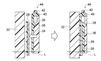
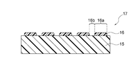
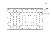
- FIG. It is a cross-sectional schematic diagram for demonstrating fixation and immersion of the 4th laminated board using a suction jig and a back plate. It is the front schematic diagram which observed the structure containing the 4th laminated board shown by FIG. 2A in the state which removed the front plate etc. from the front plate side of the suction jig. It is a cross-sectional schematic diagram which shows one aspect of the adhesive sheet prepared by this invention. It is an upper surface schematic diagram of the adhesive sheet shown by FIG. 3A.
- the method of manufacturing a semiconductor package according to the present invention includes (a) preparation of an adhesive sheet, (b) preparation of a first laminate, (c) lamination of a reinforcing sheet, (d) peeling of a first support substrate, (e) semiconductor. Each step of mounting the chip, (f) dipping in a solution, (g) dissolving or softening the adhesive layer, and (h) peeling the reinforcing sheet is included.
- pressure-sensitive adhesive sheet As shown in FIGS. 3A and 3B, pressure-sensitive adhesive including a base material sheet 15 and a soluble pressure-sensitive adhesive layer 16 provided in at least one surface of the base material sheet 15 in an intermittent pattern. Prepare the sheet 17. Details of the adhesive sheet 17 will be described later.
- the pressure-sensitive adhesive sheet includes an "adhesive pressure-sensitive adhesive sheet" used for adhering the base sheet itself to an adherend via an adhesive layer, and an adhesive layer transferred to an adherend or a second base sheet.
- transfer-type pressure-sensitive adhesive sheet used to impart adhesiveness to an adherend or a second substrate sheet by peeling the initial substrate sheet.
- the pressure-sensitive adhesive sheet 17 prepared in the present invention may be either an adhesive pressure-sensitive adhesive sheet or a transfer pressure-sensitive adhesive sheet.
- a first laminated body 14 having the rewiring layer 12 on the first support substrate 10 is prepared.
- the first support substrate 10 serves as a base for forming the redistribution layer 12.
- the first support substrate 10 may be in the form of a so-called metal foil with a carrier, and a known layer structure can be adopted.
- the first support substrate 10 may include a base material, a release layer, and a metal layer in that order.
- a laminated sheet disclosed in Patent Document 3 International Publication No. 2018/097265
- the base material of this laminated sheet can be made of a resin film, glass or ceramics).
- the redistribution layer 12 is preferably formed on the metal layer surface of the first supporting substrate 10.
- the rewiring layer means a layer including an insulating layer and a wiring layer formed inside and / or on the surface of the insulating layer.
- the chip electrodes arranged on the semiconductor chip and the terminals arranged on the printed wiring board at a pitch larger than that of the chip electrodes can be electrically connected.
- the redistribution layer 12 may be formed according to a known method and is not particularly limited.
- the rewiring layer 12 can be formed by alternately laminating the insulating layers and the wiring layers into a multi-layer by the build-up method described above.
- the second support substrate 18 has the soluble adhesive layer 16 on the surface of the first laminate 14 on the rewiring layer 12 side.
- the second stacked body 20 bonded via the is obtained.
- the second laminated body 20 can be obtained by attaching the second support substrate 18 to the surface of the first laminated body 14 on the rewiring layer 12 side using the adhesive sheet 17.
- the redistribution layer 12 can be reinforced by the second support substrate 18 so as not to be greatly curved.
- the second support substrate 18 functions as a reinforcing sheet, it is possible to avoid disconnection and peeling of the wiring layer on the surface and / or inside of the rewiring layer 12 and improve the connection reliability of the rewiring layer 12. it can. Further, since the curvature is effectively prevented or suppressed, the flatness (coplanarity) of the surface of the redistribution layer 12 can be improved.
- the pressure-sensitive adhesive sheet 17 is an adhesive pressure-sensitive adhesive sheet
- the pressure-sensitive adhesive sheet 17 is attached to the surface of the first laminate 14 on the rewiring layer 12 side, and the base material sheet 15 itself is used as the second support substrate 18.
- the pressure-sensitive adhesive sheet 17 is a transfer-type pressure-sensitive adhesive sheet
- the pressure-sensitive adhesive sheet 17 is attached to the second supporting substrate 18 or the first multilayer body 14 prior to the bonding of the first laminated body 14 and the second supporting substrate 18. It is preferable that the base material sheet 15 is peeled off while the soluble adhesive layer 16 is transferred to the second supporting substrate 18 or the first laminated body 14 by pasting.
- the transfer method is not particularly limited, and a known method such as roll lamination can be adopted.
- the second supporting substrate 18 preferably has a Vickers hardness lower than that of the first supporting substrate 10. As a result, the second support substrate 18 itself bends, so that the stress that may occur during stacking or peeling can be well escaped, and as a result, the curvature of the redistribution layer 12 can be effectively prevented or suppressed. ..
- the Vickers hardness of the second support substrate 18 is preferably 2% or more and 99% or less of the Vickers hardness of the rewiring layer 12, more preferably 6% or more and 90% or less, and further preferably 10% or more and 85% or less. ..
- the Vickers hardness of the second support substrate 18 is preferably 50 HV or more and 700 HV or less, more preferably 150 HV or more and 550 HV or less, and further preferably 170 HV or more and 500 HV or less.
- the Vickers hardness is measured according to the "Vickers hardness test" described in JIS Z 2244-2009.
- the Vickers hardness HV of various materials are illustrated below: Sapphire glass (2300 HV), cemented carbide (1700 HV), cermet (1650 HV), quartz (quartz) (1103 HV), SKH56 (high speed tool).
- the material of the second support substrate 18 is not particularly limited, but resin, metal, glass, or a combination thereof is preferable.
- the resin include an epoxy resin, a polyimide resin, a polyethylene resin, and a phenol resin, and a prepreg composed of such a resin and a fiber reinforcing material may be used.
- the metal include stainless steel and copper alloys (for example, bronze, phosphor bronze, copper nickel alloy, and copper titanium alloy) from the viewpoint of the Vickers hardness and the spring limit value Kb 0.1 , but they have chemical resistance. From the viewpoint, stainless steel is particularly preferable.
- the form of the second support substrate 18 is not limited to a sheet shape as long as the curvature of the redistribution layer 12 can be prevented or suppressed, and other forms such as a film, a plate, and a foil may be used, and preferably a sheet or a plate is used. It is a form.
- the second support substrate 18 may be a laminate of these sheets, films, plates, foils and the like. Typical examples of the second support substrate 18 include a metal sheet, a resin sheet (particularly a hard resin sheet), and a glass sheet.
- the thickness of the second support substrate 18 is preferably 10 ⁇ m or more and 1 mm or less, more preferably 50 ⁇ m or more and 800 ⁇ m or less, from the viewpoint of maintaining the strength of the second support substrate 18 and easiness of handling the second support substrate 18. It is preferably 100 ⁇ m or more and 600 ⁇ m or less.
- the second support substrate 18 is a metal sheet (for example, a stainless steel sheet)
- the ten-point average roughness Rz-jis (JIS B 0601-2001) of the surface of the metal sheet that is in close contact with the soluble adhesive layer 16 is used.
- (D) Peeling of First Support Substrate As shown in FIG. 1A (iii), the side where the first support substrate 10 is peeled from the second stacked body 20 and the redistribution layer 12 is separated from the second support substrate 18.
- the third laminated body 22 whose surface is exposed is obtained.
- the base material, the peeling layer, and the like that form the first supporting substrate 10 are peeled and removed from the rewiring layer 12.
- This peeling and removal is preferably performed by physical peeling.
- the physical peeling method is a method of separating the first support substrate 10 by peeling it from the rewiring layer 12 with a hand, a jig, a machine, or the like.
- the rewiring layer 12 can be prevented from being largely curved locally. That is, the second support substrate 18 can reinforce the rewiring layer 12 to resist the peeling force while the first support substrate 10 is peeled off, and can more effectively prevent or suppress the bending. In this way, disconnection or peeling of the wiring layer on the inside and / or the surface of the rewiring layer 12 which may be caused by the curvature can be avoided, and the connection reliability of the rewiring layer 12 can be improved. Further, since the curvature is effectively prevented or suppressed, the flatness (coplanarity) of the surface of the redistribution layer 12 can be improved.
- the metal layer that may remain on the surface of the third stacked body 22 after the peeling of the first supporting substrate 10 is removed by etching.
- the etching of the metal layer may be performed based on a known method such as flash etching.
- each end surface of the fourth stacked body 28 may be different.
- both end faces on the long side may be set as the upper end face and the lower end face, respectively, and both end faces on the short side may be set as the upper end face and the lower end face, respectively. Good.
- both ends on the long side are extended.
- the surfaces are an upper end surface and a lower end surface, respectively.
- the surface of the rewiring layer 12 on the side away from the second supporting substrate 18 may be subjected to pretreatment.
- pretreatment a chip electrode arranged on a semiconductor chip and The formation of electrodes (for example, columnar electrodes) for connection may be mentioned.
- the formation of the electrodes may be carried out by using a known method, and for example, it can be preferably carried out by selectively forming electrolytic copper plating using a dry film resist.
- Examples of the semiconductor chip 24 include semiconductor elements, chip capacitors, resistors, and the like.
- Examples of chip mounting methods include a flip chip mounting method and a die bonding method.
- the flip-chip mounting method is a method of bonding the mounting pad of the semiconductor chip 24 and the wiring layer of the rewiring layer 12.
- Columnar electrodes (pillars), solder bumps, etc. may be formed on this mounting pad, and NCF (Non-Conductive Film), which is a sealing resin film, is attached to the surface of the rewiring layer 12 before mounting. Good.
- the joining is preferably performed using a low melting point metal such as solder, but an anisotropic conductive film or the like may be used.
- the die bonding adhesion method is a method of adhering the surface of the semiconductor chip 24 opposite to the mounting pad surface to the wiring layer.
- a paste or film which is a resin composition containing a thermosetting resin and a heat conductive inorganic filler.
- the semiconductor chip 24 is resin-sealed with the sealing material 26 as shown in FIG. 1B (iv). By doing so, the rigidity of the entire stacked body of the redistribution layer 12 and the semiconductor chip 24 can be further improved.
- the encapsulating material 26 may be made of a known material (for example, epoxy resin) used for resin encapsulation of the semiconductor chip, and is not particularly limited.
- FIG. 1B Immersion in Dissolution Solution
- a part of the fourth laminate 28 is immersed in a solution capable of dissolving the soluble adhesive layer 16 (that is, a dissolution solution).
- a dissolution solution that is, a dissolution solution.
- the right end surface and the left end surface of the fourth stacked body 28 are sealed with a pair of sealing members 36, and the fourth stacked body 28 is lowered at the lower end surface.
- the lower end surface is selectively immersed in the solution L at an angle such that the upper end surface faces upward.
- the solution L permeates into the internal space between the second support substrate 18 and the rewiring layer 12 (hereinafter, may be simply referred to as “internal space”) in the step of dissolving or softening the adhesive layer described below.
- internal space the solution L spreads evenly from the lower end surface to the upper end surface without leaking from the left and right end surfaces of the fourth stacked body 28.
- the soluble adhesive layer 16 can be efficiently dissolved or softened.
- the lower end surface of the fourth stacked body 28 is selectively immersed in the solution L, contact with the solution L is made more difficult than in the case where the entire fourth stacked body 28 is immersed in the solution L.
- the damage to the semiconductor chip 24 and the sealing material 26 is effectively suppressed.
- the conventional methods have limited the types of usable dissolution liquids, such as the use of a dissolution liquid in a pH range that is unlikely to adversely affect devices and the like.
- the damage given to the semiconductor chip 24 and the like can be suppressed by adopting the above-mentioned aspect, it is possible to flexibly adopt a solution having a property capable of more effectively dissolving the soluble adhesive layer 16. It will be possible.
- the length from the lower end surface to the upper end surface of the fourth stacked body 28 is set to 100%, and only the lower region within the range of more than 0% and 90% or less of the length from the lower end surface is immersed in the solution L. More preferably, 1% or more and 70% or less, still more preferably 1% or more and 50% or less, still more preferably 1% or more and 30% or less, particularly preferably 2% or more and 20% or less, particularly preferably 2% or more. It is 10% or less, most preferably 2% or more and 5% or less.
- the lower region within the range of 200 mm in length from the lower end surface of the fourth laminate 28 into the solution L, more preferably 100 mm, further preferably 50 mm, and even more preferably still.
- Is 30 mm particularly preferably 20 mm, particularly preferably 10 mm and most preferably 5 mm.
- one surface side of the fourth stacked body 28 is fixed by contacting the back plate 32.
- the surface of the fourth stacked body 28 that is in contact with the back plate 32 may be the rewiring layer 12 side or the second support substrate 18 side.
- the fourth jig 28 is sandwiched between the suction jig 44 and the back plate 32 for sealing.
- the suction jig 44 includes a front plate 34, a pair of sealing members 36, a second sealing member 38, an upper cap 40, and a suction port 42.
- the pair of sealing members 36 are provided on the front plate 34 in parallel with each other and spaced apart from each other.
- the second sealing member 38 is provided on the front plate 34 so as to be suspended between the pair of sealing members 36, and has an internal space between the second support substrate 18 and the redistribution layer 12 of the fourth stacked body 28. It plays a role of generating a pressure difference with the solution L and promoting penetration of the solution L into the internal space.
- the upper cap 40 is connected to the upper end of the front plate 34 and / or the upper end of the pair of sealing members 36, and together with the front plate 34, the pair of sealing members 36, the second sealing member 38, and the back plate 32. It is possible to form a closed space for decompression.
- the suction port 42 is provided in the upper cap 40.
- a pump (not shown) is connected to the suction port 42. As described above, by using the suction jig 44 having a simple structure and easily attached and detached, the soluble adhesive layer 16 can be more efficiently dissolved or softened
- Preferred examples of the sealing member include a rubber member, an adhesive film, an elastomer, and a combination thereof. And more preferably a rubber member.
- the rubber constituting the rubber member include EPDM (ethylene propylene diene rubber), silicone rubber, fluorine-containing rubber, and a combination thereof. , And more preferably silicone rubber. Further, by using the sealing member having excellent surface smoothness, it is possible to further improve the adhesiveness with the fourth stacked body 28.
- the maximum height Rz of the surface of the sealing member that contacts the fourth laminate 28 is 0.01 ⁇ m or more and 500 ⁇ m or less, and more preferably the maximum height Rz is measured in accordance with JIS B0601-2001.
- the thickness is 0.02 ⁇ m or more and 100 ⁇ m or less, more preferably 0.03 ⁇ m or more and 60 ⁇ m or less, and particularly preferably 0.05 ⁇ m or more and 20 ⁇ m or less.
- the back plate 32 preferably has alkali resistance. This is because it is assumed that the back plate 32 also contacts the solution L as shown in FIGS. 2A and 2B. However, as described later, the soluble adhesive layer 16 preferably contains an alkali-soluble resin. This is because an alkaline solution is typically used as the solution L. From this viewpoint, the back plate 32 is preferably made of vinyl chloride. Further, from the viewpoint of further enhancing the adhesion with the fourth laminate 28, the maximum height Rz measured on the surface of the back plate 32 in contact with the fourth laminate 28 according to JIS B0601-2001 is 0.
- It is preferably 0.01 ⁇ m or more and 500 ⁇ m or less, more preferably 0.02 ⁇ m or more and 100 ⁇ m or less, still more preferably 0.03 ⁇ m or more and 60 ⁇ m or less, and particularly preferably 0.05 ⁇ m or more and 20 ⁇ m or less.
- the solution L may be appropriately selected according to the material of the soluble adhesive layer 16 and has a desired dissolving power, and is not particularly limited.
- the solution L may be an alkaline solution.
- alkaline solutions include sodium hydroxide solution and / or potassium hydroxide solution.
- the preferred concentration of these solutions is 0.5% by weight or more and 50% by weight or less. Within this range, the alkalinity will be high, the dissolving power will be improved, and sodium hydroxide and / or potassium hydroxide will be less likely to precipitate even when the room temperature is low when the solution is used.
- an organic substance for example, ethanolamine
- aqueous solution is alkaline
- water or an aqueous solution may be used as the solution.
- an organic solvent for example, 2-propanol
- the preferable addition amount of this organic solvent is 5% by weight or more and 50% by weight or less based on 100% by weight of the alkaline solution. Within this range, the volatilization amount during the work is reduced while the shortening of the dissolution time is desirably realized, so that the concentration of the alkaline substance can be easily controlled and the safety is improved.
- a preferred organic solvent is alcohol, and preferred examples of alcohol include 2-propanol, methanol, ethanol, and 2-butanol.
- An appropriate amount of surfactant may be added to the alkaline solution. Since the permeability and wettability of the solution with respect to the resin are improved by adding the surfactant, the dissolution time of the soluble adhesive layer 16 can be further shortened.
- the kind of the surfactant is not particularly limited and may be any kind.
- any of anionic, cationic and nonionic surfactants can be used.
- the internal space is filled with the solution L, and the soluble adhesive layer 16 existing in the internal space comes into contact with the solution L, whereby the soluble adhesive layer 16 is dissolved or softened.
- the solution L effectively permeates into the gaps in the intermittent pattern of the soluble adhesive layer 16 to promote dissolution or softening of the soluble adhesive layer 16.
- the dissolution liquid is forcibly permeated by applying a pressure difference between the internal space where the soluble adhesive layer 16 is present and the dissolution liquid, so that the entire laminate is dissolved in the dissolution liquid.
- the pressure difference between the internal space and the solution L is preferably 5 kPa or more, more preferably 20 kPa or more and 100 kPa or less, as measured by a gauge pressure gauge. It is preferably 40 kPa or more and 100 kPa or less, and particularly preferably 60 kPa or more and 100 kPa or less.
- the pressure difference may be given by pressurizing the solution L, but it is preferable to be given by depressurizing the internal space because it can be realized with a simple structure. That is, the decompression of the internal space can be preferably performed using the pump connected to the upper end surface of the fourth stacked body 28.
- preferred pumps include ejector pumps, rotary pumps, diaphragm pumps, aspirator pumps and combinations thereof.
- a pump may be directly connected to the upper end surface of the fourth stacked body 28 to perform depressurization, but as shown in FIGS. 2A and 2B, the suction jig 44 is used to seal the depressurized seal at the upper end portion of the fourth stacked body 28. It is preferable to form a space and connect a pump to the suction port 42 of the suction jig 44 to reduce the pressure.
- the second support substrate 18 can be peeled off in an extremely short time while minimizing the stress applied to the redistribution layer 12.
- the stress applied to the redistribution layer 12 disconnection of the wiring in the redistribution layer 12 or disconnection of the mounting portion can be effectively avoided.
- the adhesive sheet 17 used in the method of the present invention includes the base sheet 15 and the fusible sheet provided with an intermittent pattern on at least one surface of the base sheet 15. And an adhesive layer 16.
- the soluble adhesive layer 16 may be provided on both sides of the base material sheet 15.
- the intermittent pattern means a shape in which the soluble adhesive layer 16 is present intermittently (interruptedly), and the adhesive region 16a where the soluble adhesive layer 16 exists and the non-adhesive region 16b where the soluble adhesive layer 16 does not exist ( Space).
- the intermittent pattern is preferably an island-shaped or stripe-shaped pattern, and more preferably an island-shaped pattern.
- the island-shaped pattern means a shape in which the individual adhesive regions 16a are surrounded by the non-adhesive regions 16b existing around them.
- Specific shapes of the individual adhesive regions 16a forming the island pattern include various shapes such as polygons and circles, and polygons in which straight contour lines such as star polygons are intricate, The shape may be a complicated shape with curved contour lines.
- the diameter of the circumscribed circle of each adhesive region 16a is preferably 0.1 mm or more and 10 mm or less, more preferably 0.1 mm or more and 5.0 mm or less, More preferably, it is 0.1 mm or more and 2.0 mm or less.
- the stripe width of each adhesive region 16a is preferably 0.1 mm or more and 10 mm or less, more preferably 0.1 mm or more and 5.0 mm or less, More preferably, it is 0.1 mm or more and 2.0 mm or less.
- the island pattern is preferably a dot pattern, and the shape of each dot is typically a circle, but it may be a shape close to a circle.
- the dot diameter which is defined as the diameter of the circumscribing circle of each dot forming the dot pattern, is preferably 10 mm or less, more preferably 0.1 mm or more and 5.0 mm or less, still more preferably 0.1 mm or more. It is 0 mm or less. By doing so, the surface area of the soluble adhesive layer 16 is increased and the solubility is improved. As a result, the peelability is improved.
- the soluble adhesive layer 16 preferably has a thickness of 0.5 ⁇ m or more and 50 ⁇ m or less, more preferably 1.0 ⁇ m or more and less than 30 ⁇ m, further preferably 1.0 ⁇ m or more and 20 ⁇ m or less, particularly preferably 2.0 ⁇ m or more and 15 ⁇ m or less. , And most preferably 3.0 ⁇ m or more and 10 ⁇ m or less.
- the thickness is within the above range, the solution quickly permeates into the gaps of the pattern of the soluble adhesive layer 16, so that the dissolution or softening of the soluble adhesive layer 16 is promoted and, at the same time, the rewiring layer 12 of the intermittent pattern is formed. It is possible to reduce the indentation.
- the soluble adhesive layer 16 may remain in the rewiring layer 12, but if the thickness of the soluble adhesive layer 16 is 7.0 ⁇ m or less, there is an advantage that the indentation hardly remains in the rewiring layer 12 after compression molding. ..
- the soluble adhesive layer 16 has a dot pattern, if the dot diameter is 0.7 mm or less and the thickness of the soluble adhesive layer 16 is 1.0 ⁇ m or more and 7.0 ⁇ m or less, indentation is reduced. It is particularly preferable because both of releasability can be more effectively realized.
- the distance between the centers of the circumscribing circles of the adhesive areas 16a is preferably larger than the average diameter of the circumscribing circles, in order to ensure a sufficient gap between the individual adhesive areas 16a.
- the distance between the centers of the circumscribing circles of the adhesive region 16a is preferably more than 0.1 mm and 20 mm or less, more preferably 0.2 mm or more and 10 mm or less, and further preferably 0.3 mm or more and 5.0 mm or less. It is particularly preferably 0.4 mm or more and 2.0 mm or less. With such a range, the dissolution liquid quickly penetrates into the gaps between the patterns of the soluble pressure-sensitive adhesive layer 16, so that the releasability is improved.
- the island-like pattern may be composed of one or more clusters that result in a polygonal, circular, toric, strip-like or lattice-like pattern as a whole, each of the clusters having three or more adhesive regions. It may be composed of an assembly of 16a.
- the soluble adhesive layer 16 is, of course, a layer that exhibits adhesiveness at room temperature and can be dissolved or softened by contact with a solution. Therefore, the soluble adhesive layer 16 preferably contains a solution-soluble resin, for example, an acid-soluble resin or an alkali-soluble resin. This solution-soluble resin can be efficiently dissolved or softened by contact with a solution, so that the second support substrate 18 can be more effectively peeled from the rewiring layer 12. ..
- the -A preferred solution-soluble resin is an alkali-soluble resin. This is because it is assumed that a neutral or acidic solution is used in the washing process or the like in the manufacture of the semiconductor package, and therefore it is desired that the solution-soluble resin is not dissolved in the neutral or acidic solution.
- the alkali-soluble resin particularly preferably contains a polymer containing at least one of a carboxyl group and a phenolic hydroxyl group. Since such a polymer is particularly soluble in an alkaline solution, it promotes the dissolution of the soluble adhesive layer 16 and enables the second support substrate 18 to be peeled from the rewiring layer 12 in a shorter time.
- Examples of the polymer containing at least one of a carboxyl group and a phenolic hydroxyl group include an acrylic resin containing a carboxyl group and a phenol novolac resin containing a phenolic hydroxyl group.
- the acrylic resin-based pressure-sensitive adhesive copolymerizes an acrylic monomer having a carboxyl group and an unsaturated double bond in the molecule (for example, acrylic acid or methacrylic acid) with ethyl acrylate or butyl acrylate. It can be synthesized by By adjusting the type and ratio of the acrylic monomer during the synthesis, the adhesive strength of the soluble adhesive layer 16 and the solubility in the alkaline solution can be controlled.
- Control of the adhesive strength of the soluble adhesive layer 16 and the solubility in an alkaline solution can also be performed by adding a resin (for example, an epoxy resin) that causes a crosslinking reaction of a carboxyl group to an acrylic resin containing a carboxyl group.
- a resin for example, an epoxy resin
- a phenol novolac resin containing a phenolic hydroxyl group is used as the alkali-soluble resin, the adhesive strength of the soluble adhesive layer 16 is weakened by using this resin alone. Therefore, by mixing a tackifier such as rosin, It is preferable to impart appropriate tackiness.
- Alkali-soluble resin may be added with alkali in advance. By doing so, it becomes possible to dissolve or soften the soluble adhesive layer 16 using water or an aqueous solution as a solution. That is, when the soluble adhesive layer 16 is brought into contact with water or an aqueous solution, the liquid such as water is changed to alkaline by the alkali added in advance, and thereby the soluble adhesive layer 16 containing the alkali-soluble resin is dissolved or It becomes possible to soften.
- the form of the base material sheet 15 is not limited to what is generally called a sheet, but may be another form such as a film, a plate, or a foil.
- the base sheet 15 may be a laminate of these sheets, films, plates, foils and the like.
- the surface of the base material sheet 15 to which the soluble adhesive layer 16 is applied is subjected to a polishing treatment, a release agent application,
- the surface treatment may be performed in advance by a known method such as plasma treatment.
- the base material sheet 15 is preferably composed of at least one resin of polyethylene terephthalate (PET) and polyethylene (PE), and more preferably polyethylene terephthalate (PET).
- PET polyethylene terephthalate
- PET polyethylene
- PET polyethylene terephthalate
- the base material sheet 15 may have a function of holding the soluble adhesive layer 16 and a function of transferring the soluble adhesive layer 16 to the second supporting substrate 18 which is separately prepared.
- the base sheet 15 of this embodiment is suitable for such applications.
- the thickness of the base material sheet 15 is preferably 10 ⁇ m or more and 200 ⁇ m or less, more preferably 20 ⁇ m or more and 150 ⁇ m or less, and further preferably 25 ⁇ m or more and 75 ⁇ m or less.
- the base material sheet 15 may be similar to the second support substrate 18, and the preferable embodiment of the second support substrate 18 described above is the base material sheet 15. Is also true.
- the base material sheet 15 has a function of holding the soluble pressure-sensitive adhesive layer 16, and also improves handling of the rewiring layer 12 and prevents bending in the manufacturing process of the semiconductor package.
- the function as a reinforcing sheet is desired, but the base material sheet 15 of this embodiment is suitable for such use.
Landscapes
- Engineering & Computer Science (AREA)
- Manufacturing & Machinery (AREA)
- Microelectronics & Electronic Packaging (AREA)
- Laminated Bodies (AREA)
- Production Of Multi-Layered Print Wiring Board (AREA)
- Container, Conveyance, Adherence, Positioning, Of Wafer (AREA)
- Encapsulation Of And Coatings For Semiconductor Or Solid State Devices (AREA)
Abstract
Description
(a)基材シートと、該基材シートの少なくとも一方の面に間欠パターンで設けられた可溶性粘着層を備えた、粘着シートを用意する工程と、
(b)第1支持基板上に再配線層を備えた第1積層体を作製する工程と、
(c)前記粘着シートを用いて、前記第1積層体の前記再配線層側の表面に、第2支持基板が前記可溶性粘着層を介して結合された第2積層体を得る工程と、
(d)前記第2積層体から前記第1支持基板を剥離して、前記再配線層の前記第2支持基板から離れた側の表面が露出した第3積層体を得る工程と、
(e)前記第3積層体の前記再配線層側の表面に半導体チップを実装し、かつ、前記半導体チップを樹脂封止して、上端面、下端面、右端面及び左端面からなる外周端面を備えた第4積層体を得る工程と、
(f)前記第4積層体の前記右端面及び前記左端面を1対の封止部材で封止し、前記第4積層体を前記下端面が下にかつ前記上端面が上になるような角度で、前記下端面を溶液に選択的に浸漬させる工程と、
(g)前記第4積層体の前記第2支持基板及び前記再配線層間の内部空間と、前記溶液との間に圧力差を与えて、該圧力差により前記溶液を前記内部空間内に浸透させ、それにより前記可溶性粘着層を溶解又は軟化させる工程と、
(h)前記可溶性粘着層が溶解又は軟化された状態で、前記第4積層体から前記第2支持基板を剥離して半導体パッケージを得る工程と、
を含む、方法が提供される。
図3A及び図3Bに示されるように、基材シート15と、基材シート15の少なくとも一方の面に間欠パターンで設けられた可溶性粘着層16とを備えた、粘着シート17を用意する。粘着シート17の詳細については後述するものとする。なお、粘着シートには、粘着層を介して基材シート自体を被着体に接着させるために用いられる「接着型粘着シート」と、粘着層を被着体又は第二の基材シートに転写させて当初の基材シートを剥離することで、被着体又は第二の基材シートに粘着性を付与するために用いられる「転写型粘着シート」の2つのタイプが存在する。この点、本発明で用意する粘着シート17は接着型粘着シート及び転写型粘着シートのいずれであってもよい。
図1A(i)に示されるように、第1支持基板10上に再配線層12を備えた第1積層体14を作製する。第1支持基板10は再配線層12を形成するためのベースとなるものである。第1支持基板10は、いわゆるキャリア付金属箔の形態であってもよく、公知の層構成が採用可能である。第1支持基板10は、基材、剥離層及び金属層を順に備えるものであってもよく、例えば特許文献3(国際公開第2018/097265号)に開示される積層シートを好ましく用いることができる(この積層シートの基材は樹脂フィルム、ガラス又はセラミックスで構成されうる)。この場合、再配線層12が第1支持基板10の金属層表面に作製されるのが好ましい。
図1A(ii)に示されるように、粘着シート17を用いて、第1積層体14の再配線層12側の表面に、第2支持基板18が可溶性粘着層16を介して結合された第2積層体20を得る。例えば、第1積層体14の再配線層12側の表面に粘着シート17を用いて第2支持基板18を貼り付けることにより、第2積層体20を得ることができる。こうすることで、再配線層12は第2支持基板18によって大きく湾曲されないように補強されることができる。すなわち、第2支持基板18が補強シートとして機能するため、再配線層12の表面及び/又は内部の配線層の断線や剥離を回避して、再配線層12の接続信頼性を向上することができる。また、湾曲が効果的に防止ないし抑制されることで、再配線層12表面の平坦性(コプラナリティ)を向上することができる。
図1A(iii)に示されるように、第2積層体20から第1支持基板10を剥離して、再配線層12の第2支持基板18から離れた側の表面が露出した第3積層体22を得る。こうすることで、例えば第1支持基板10を構成する基材及び剥離層等が再配線層12から剥離除去される。この剥離除去は物理的な剥離により行われるのが好ましい。物理的剥離法は、手や治工具、機械等で第1支持基板10を再配線層12から引き剥がすことにより分離する手法である。このとき、可溶性粘着層16を介して密着した第2支持基板18が再配線層12を補強していることで、再配線層12が局部的に大きく湾曲するのを防止することができる。すなわち、第2支持基板18は、第1支持基板10が剥離される間、引き剥がし力に抗すべく再配線層12を補強し、湾曲をより一層効果的に防止ないし抑制することができる。こうして湾曲により引き起こされることがある再配線層12の内部及び/又は表面の配線層の断線や剥離を回避して、再配線層12の接続信頼性を向上することができる。また、湾曲が効果的に防止ないし抑制されることで、再配線層12表面の平坦性(コプラナリティ)を向上することができる。なお、第1支持基板10が金属層を含む場合には、第1支持基板10の剥離後に第3積層体22の表面に残留しうる金属層をエッチングにより除去するのが好ましい。金属層のエッチングはフラッシュエッチング等の公知の手法に基づき行えばよい。
図1B(iv)に示されるように、第3積層体22の再配線層12側の表面に半導体チップ24を実装し、かつ、半導体チップ24を封止材26で樹脂封止して、上端面、下端面、右端面及び左端面からなる外周端面を備えた第4積層体28を得る。本発明の方法においては、再配線層12の表面に可溶性粘着層16を介して第2支持基板18を積層することで、半導体チップ24の実装に有利となる優れた表面平坦性(コプラナリティ)を再配線層12の第2支持基板18から離れた側の表面において実現することができる。すなわち、半導体チップ24の実装時においても、再配線層12は第2支持基板18によって局部的に大きく湾曲されずに済む。その結果、半導体チップ24の接続歩留まりを高くすることができる。なお、第4積層体28の各端面の長さはそれぞれ異なっていてもよい。例えば、第4積層体28が矩形状の場合、長辺側の両端面をそれぞれ上端面及び下端面と設定してもよく、短辺側の両端面をそれぞれ上端面及び下端面と設定してもよい。この点、後述する粘着層の溶解又は軟化工程において、第4積層体28の上端面に接続されたポンプを用いて吸引を行う場合には、吸引する面積を広げる観点から、長辺側の両端面をそれぞれ上端面及び下端面とするのが好ましい。
図1B(v)に示されるように、第4積層体28の一部を、可溶性粘着層16を溶解可能な溶液(すなわち溶解液)に浸漬させる。この操作は、図2A及び図2Bに示されるように、第4積層体28の右端面及び左端面を1対の封止部材36で封止し、第4積層体28を下端面が下にかつ上端面が上になるような角度で、下端面を溶液Lに選択的に浸漬させることにより行う。こうすることで、後述する粘着層の溶解又は軟化工程において、溶液Lを第2支持基板18及び再配線層12間の内部空間(以下、単に「内部空間」と称することがある)内に浸透させた際に、溶液Lが第4積層体28の左右端面から漏れ出すことなく、下端面から上端面に向かって万遍なく行き渡る。その結果、可溶性粘着層16の溶解又は軟化を効率良く行うことが可能となる。さらに、本発明の方法では、第4積層体28の下端面を溶液Lに選択的に浸漬させるため、第4積層体28の全体を溶液Lに浸漬させる場合と比べて、溶液Lとの接触により半導体チップ24及び封止材26が受けるダメージが効果的に抑制される。この点、従来の方法では、デバイス等に悪影響を及ぼしにくいpH領域の溶解液を用いる等、使用可能な溶解液の種類が制限されていた。一方、本発明の方法では、上記態様とすることで半導体チップ24等に与えるダメージを抑制できるため、可溶性粘着層16をより効果的に溶解可能な性質を有する溶解液を柔軟に採用することが可能となる。
第4積層体28の下端面を溶液Lに浸漬させた状態で、第4積層体28の第2支持基板18及び再配線層12間の内部空間と、溶液Lとの間に圧力差を与えて、溶液Lを内部空間内に浸透させる。こうして可溶性粘着層16を溶解又は軟化させる。すなわち、第4積層体28の内部空間内を減圧する、及び/又は溶液Lを加圧することにより、第4積層体28の下端面付近に存在する溶液Lが、第4積層体28の上端面側に向かって内部空間内を上昇する。その結果、内部空間内が溶液Lで満たされ、内部空間内に存在する可溶性粘着層16と溶液Lとが接触することで、可溶性粘着層16が溶解又は軟化する。この点、可溶性粘着層16は間欠パターンで構成されているので、溶液Lが可溶性粘着層16の間欠パターンの隙間に効果的に浸透して、可溶性粘着層16の溶解又は軟化が促進される。このように、本発明の方法では、可溶性粘着層16が存在する内部空間と溶解液との間に圧力差を与えることで溶解液の浸透を強制的に行うため、積層体の全体を溶解液に浸漬させることで毛細管現象により溶解液を粘着層の隙間に徐々に浸透させる従来の方法と比べて、粘着層の溶解又は軟化を極めて短時間で行うことができる。
図1B(vi)に示されるように、可溶性粘着層16が溶解又は軟化された状態で、第4積層体28から第2支持基板18を剥離して、半導体パッケージ30を得る。第2支持基板18は可溶性粘着層16の溶解又は軟化に起因して極めて剥離しやすい状態となっているため、手や治工具、機械等で第2支持基板18を第4積層体28から軽く引き剥がすことにより極めて容易に分離することができる。なお、第2支持基板18は、可溶性粘着層16の溶解に起因して自然剥離した状態となっていてもよい。いずれにしても、本発明の方法によれば、再配線層12に与える応力を最小化しながら極めて短時間で第2支持基板18の剥離を行うことができる。こうして再配線層12に加わる応力が最小化されることで、再配線層12における配線の断線や実装部の断線を効果的に回避することができる。
図3A及び図3Bを参照しつつ上述したとおり、本発明の方法に用いられる粘着シート17は、基材シート15と、基材シート15の少なくとも一方の面に間欠パターンで設けられた可溶性粘着層16とを備える。可溶性粘着層16は基材シート15の両面に設けられてもよい。間欠パターンとは、可溶性粘着層16が間欠的(途切れ途切れ)に存在する形状を意味し、可溶性粘着層16が存在する粘着性領域16aと、可溶性粘着層16が存在しない非粘着性領域16b(例えば空間)とによって形成される。間欠パターンは島状又はストライプ状のパターンであるのが好ましく、より好ましくは島状のパターンである。島状のパターンとは、個々の粘着性領域16aが、その周りに存在する非粘着性領域16bによって取り囲まれた形状を意味する。島状のパターンを構成する個々の粘着性領域16aの具体的形状としては、多角形、円形等の様々な形状が挙げられ、星形多角形のような直線の輪郭線が入り組んだ多角形、曲線の輪郭線が入り組んだ異形状であってもよい。
Claims (19)
- 半導体パッケージの製造方法であって、
(a)基材シートと、該基材シートの少なくとも一方の面に間欠パターンで設けられた可溶性粘着層を備えた、粘着シートを用意する工程と、
(b)第1支持基板上に再配線層を備えた第1積層体を作製する工程と、
(c)前記粘着シートを用いて、前記第1積層体の前記再配線層側の表面に、第2支持基板が前記可溶性粘着層を介して結合された第2積層体を得る工程と、
(d)前記第2積層体から前記第1支持基板を剥離して、前記再配線層の前記第2支持基板から離れた側の表面が露出した第3積層体を得る工程と、
(e)前記第3積層体の前記再配線層側の表面に半導体チップを実装し、かつ、前記半導体チップを樹脂封止して、上端面、下端面、右端面及び左端面からなる外周端面を備えた第4積層体を得る工程と、
(f)前記第4積層体の前記右端面及び前記左端面を1対の封止部材で封止し、前記第4積層体を前記下端面が下にかつ前記上端面が上になるような角度で、前記下端面を溶液に選択的に浸漬させる工程と、
(g)前記第4積層体の前記第2支持基板及び前記再配線層間の内部空間と、前記溶液との間に圧力差を与えて、該圧力差により前記溶液を前記内部空間内に浸透させ、それにより前記可溶性粘着層を溶解又は軟化させる工程と、
(h)前記可溶性粘着層が溶解又は軟化された状態で、前記第4積層体から前記第2支持基板を剥離して半導体パッケージを得る工程と、
を含む、方法。 - 前記工程(f)において、前記第4積層体の前記下端面から上端面までの長さを100%として、下端面から長さ0%超90%以下の範囲内の下方領域のみを前記溶液に浸漬させる、請求項1に記載の方法。
- 前記工程(f)が、前記第4積層体の一面側を背面板に接触させて固定する工程を含む、請求項1又は請求項2に記載の方法。
- 前記工程(g)における前記圧力差が、5kPa以上である、請求項1から請求項3までのいずれか一項に記載の方法。
- 前記工程(g)における前記圧力差が、前記第4積層体の前記上端面に接続されたポンプを用いて前記内部空間を減圧することにより与えられる、請求項1から請求項4までのいずれか一項に記載の方法。
- 前記ポンプが、エジェクタポンプ、ロータリーポンプ、ダイヤフラムポンプ及びアスピレータポンプからなる群から選択される少なくとも1種である、請求項5に記載の方法。
- 前記工程(f)が、吸引冶具と前記背面板とで前記第4積層体を挟み込むことにより行われ、前記吸引冶具が、
正面板と、
前記正面板上に互いに平行に離間して設けられる、前記1対の封止部材と、
前記正面板上に前記1対の封止部材間に懸架して設けられる、第2の封止部材と、
前記正面板の上端及び/又は前記1対の封止部材の上端に接続され、前記正面板、前記1対の封止部材、前記第2の封止部材及び前記背面板と共に、減圧用密閉空間を形成可能な上部キャップと、
前記上部キャップに設けられる吸引口と、
を備えたものであり、前記吸引口に前記ポンプが接続される、請求項5又は請求項6に記載の方法。 - 前記封止部材が、ゴム製の部材、接着フィルム、エラストマーから選択される少なくとも1種である、請求項1から請求項7までのいずれか一項に記載の方法。
- 前記封止部材がゴム製の部材であり、前記ゴムが、EPDM、シリコーンゴム及びフッ素含有ゴムからなる群から選択される少なくとも1種である、請求項8に記載の方法。
- 前記封止部材の前記第4積層体と接触する面における、JIS B0601-2001に準拠して測定される最大高さRzが0.01μm以上500μm以下である、請求項1から請求項9までのいずれか一項に記載の方法。
- 前記背面板が耐アルカリ性を有する、請求項1から請求項10までのいずれか一項に記載の方法。
- 前記背面板が塩化ビニルで構成される、請求項11に記載の方法。
- 前記背面板の前記第4積層体と接触する面における、JIS B0601-2001に準拠して測定される最大高さRzが0.01μm以上500μm以下である、請求項1から請求項12までのいずれか一項に記載の方法。
- 前記可溶性粘着層が溶液可溶型樹脂を含む、請求項1から請求項13までのいずれか一項に記載の方法。
- 前記溶液可溶型樹脂がアルカリ可溶型樹脂である、請求項1から請求項14までのいずれか一項に記載の方法。
- 前記間欠パターンが島状又はストライプ状のパターンである、請求項1から請求項15までのいずれか一項に記載の方法。
- 前記島状のパターンがドットパターンである、請求項16に記載の方法。
- 前記粘着シートが接着型粘着シートであり、前記工程(c)が、前記第1積層体の前記再配線層側の表面に前記粘着シートを貼り付けて、前記基材シート自体を前記第2支持基板として用いる工程を含む、請求項1から請求項17までのいずれか一項に記載の方法。
- 前記粘着シートが転写型粘着シートであり、前記工程(c)が、前記第1積層体と前記第2支持基板との結合に先立ち、前記第2支持基板、又は前記第1積層体に前記粘着シートを貼り付けて、前記可溶性粘着層を前記第2支持基板、又は前記第1積層体に転写するとともに、前記基材シートを剥離する工程を含む、請求項1から請求項18までのいずれか一項に記載の方法。
Priority Applications (4)
| Application Number | Priority Date | Filing Date | Title |
|---|---|---|---|
| JP2020558285A JP7382342B2 (ja) | 2018-11-21 | 2019-11-11 | 半導体パッケージの製造方法 |
| US17/292,216 US11876070B2 (en) | 2018-11-21 | 2019-11-11 | Semiconductor package manufacturing method |
| KR1020217010301A KR102667581B1 (ko) | 2018-11-21 | 2019-11-11 | 반도체 패키지의 제조 방법 |
| CN201980076424.7A CN113169133B (zh) | 2018-11-21 | 2019-11-11 | 半导体封装体的制造方法 |
Applications Claiming Priority (2)
| Application Number | Priority Date | Filing Date | Title |
|---|---|---|---|
| JP2018218382 | 2018-11-21 | ||
| JP2018-218382 | 2018-11-21 |
Publications (1)
| Publication Number | Publication Date |
|---|---|
| WO2020105485A1 true WO2020105485A1 (ja) | 2020-05-28 |
Family
ID=70773428
Family Applications (1)
| Application Number | Title | Priority Date | Filing Date |
|---|---|---|---|
| PCT/JP2019/044084 Ceased WO2020105485A1 (ja) | 2018-11-21 | 2019-11-11 | 半導体パッケージの製造方法 |
Country Status (6)
| Country | Link |
|---|---|
| US (1) | US11876070B2 (ja) |
| JP (1) | JP7382342B2 (ja) |
| KR (1) | KR102667581B1 (ja) |
| CN (1) | CN113169133B (ja) |
| TW (1) | TWI711130B (ja) |
| WO (1) | WO2020105485A1 (ja) |
Families Citing this family (3)
| Publication number | Priority date | Publication date | Assignee | Title |
|---|---|---|---|---|
| CN114122203B (zh) * | 2021-11-19 | 2023-03-14 | 东莞市中麒光电技术有限公司 | 一种利用液体表面张力实现芯片转移的方法 |
| CN115274475B (zh) * | 2022-09-27 | 2022-12-16 | 江苏芯德半导体科技有限公司 | 一种具有高密度连接层的芯片封装方法及其芯片封装结构 |
| CN116230563B (zh) * | 2023-02-28 | 2026-03-13 | 深圳市矩阵多元科技有限公司 | 封装结构制造方法及封装结构 |
Citations (3)
| Publication number | Priority date | Publication date | Assignee | Title |
|---|---|---|---|---|
| JP2002206078A (ja) * | 2001-01-11 | 2002-07-26 | Keiwa Inc | 粘着シート |
| WO2018097266A1 (ja) * | 2016-11-28 | 2018-05-31 | 三井金属鉱業株式会社 | 粘着シート及びその剥離方法 |
| WO2018097264A1 (ja) * | 2016-11-28 | 2018-05-31 | 三井金属鉱業株式会社 | 多層配線板の製造方法 |
Family Cites Families (6)
| Publication number | Priority date | Publication date | Assignee | Title |
|---|---|---|---|---|
| JP2638518B2 (ja) * | 1994-11-18 | 1997-08-06 | 日本電気株式会社 | ポリイミド多層配線基板の製造方法 |
| JP4273895B2 (ja) | 2003-09-24 | 2009-06-03 | 日立化成工業株式会社 | 半導体素子搭載用パッケージ基板の製造方法 |
| JP2013140826A (ja) * | 2011-12-28 | 2013-07-18 | Tokyo Ohka Kogyo Co Ltd | 剥離方法、および剥離液 |
| WO2014142303A1 (ja) * | 2013-03-14 | 2014-09-18 | 富士電機株式会社 | 半導体デバイスの製造方法 |
| JP2015035551A (ja) | 2013-08-09 | 2015-02-19 | ルネサスエレクトロニクス株式会社 | 半導体装置の製造方法 |
| KR101676916B1 (ko) * | 2014-08-20 | 2016-11-16 | 앰코 테크놀로지 코리아 주식회사 | 반도체 디바이스의 제조 방법 및 이에 따른 반도체 디바이스 |
-
2019
- 2019-11-11 US US17/292,216 patent/US11876070B2/en active Active
- 2019-11-11 KR KR1020217010301A patent/KR102667581B1/ko active Active
- 2019-11-11 CN CN201980076424.7A patent/CN113169133B/zh active Active
- 2019-11-11 JP JP2020558285A patent/JP7382342B2/ja active Active
- 2019-11-11 WO PCT/JP2019/044084 patent/WO2020105485A1/ja not_active Ceased
- 2019-11-19 TW TW108141872A patent/TWI711130B/zh active
Patent Citations (3)
| Publication number | Priority date | Publication date | Assignee | Title |
|---|---|---|---|---|
| JP2002206078A (ja) * | 2001-01-11 | 2002-07-26 | Keiwa Inc | 粘着シート |
| WO2018097266A1 (ja) * | 2016-11-28 | 2018-05-31 | 三井金属鉱業株式会社 | 粘着シート及びその剥離方法 |
| WO2018097264A1 (ja) * | 2016-11-28 | 2018-05-31 | 三井金属鉱業株式会社 | 多層配線板の製造方法 |
Also Published As
| Publication number | Publication date |
|---|---|
| US20210327847A1 (en) | 2021-10-21 |
| TWI711130B (zh) | 2020-11-21 |
| KR102667581B1 (ko) | 2024-05-22 |
| TW202032732A (zh) | 2020-09-01 |
| US11876070B2 (en) | 2024-01-16 |
| CN113169133A (zh) | 2021-07-23 |
| JPWO2020105485A1 (ja) | 2021-09-30 |
| CN113169133B (zh) | 2024-03-08 |
| KR20210093853A (ko) | 2021-07-28 |
| JP7382342B2 (ja) | 2023-11-16 |
Similar Documents
| Publication | Publication Date | Title |
|---|---|---|
| JP6496882B2 (ja) | 粘着シート及びその剥離方法 | |
| CN1266752C (zh) | 电路装置的制造方法 | |
| JP7382342B2 (ja) | 半導体パッケージの製造方法 | |
| KR20160020407A (ko) | 배선 기판의 제조 방법 | |
| CN116709672A (zh) | 多层布线板的制造方法 | |
| TWI516178B (zh) | A composite metal layer to which a support metal foil is attached, a wiring board using the same, and a method for manufacturing the same, and a method of manufacturing the semiconductor package using the wiring board | |
| TW201019439A (en) | Package substrate for mounting semiconductor element and method for manufacturing the package substrate | |
| KR20140131572A (ko) | 캐리어붙이 금속박 | |
| KR20040027345A (ko) | 회로 장치의 제조 방법 | |
| JP7289852B2 (ja) | 半導体パッケージの製造方法及びそれに用いられる粘着シート | |
| WO2010035864A1 (ja) | 半導体素子搭載用パッケージ基板とその製法及び半導体パッケージ | |
| TW201025535A (en) | Semiconductor element-mounting package substrate, and method for manufacturing package substrate | |
| TW201842831A (zh) | 印刷電路板製造方法 | |
| WO2010035865A1 (ja) | 半導体素子搭載用パッケージ基板及びその製造方法 | |
| CN110177427A (zh) | 一种感压胶补强逃气结构及其生产工艺 | |
| JP3925258B2 (ja) | 半導体パッケージ用基板の製造方法 | |
| CN109727877A (zh) | 一种半导体封装方法及半导体封装器件 | |
| JP2005303260A (ja) | 転写配線の製造方法 | |
| CN114883292A (zh) | 用于芯片封装的ic载板及其制备方法和芯片封装结构 | |
| KR19990049639A (ko) | 패키지기판 제조방법 |
Legal Events
| Date | Code | Title | Description |
|---|---|---|---|
| 121 | Ep: the epo has been informed by wipo that ep was designated in this application |
Ref document number: 19888121 Country of ref document: EP Kind code of ref document: A1 |
|
| ENP | Entry into the national phase |
Ref document number: 2020558285 Country of ref document: JP Kind code of ref document: A |
|
| ENP | Entry into the national phase |
Ref document number: 20217010301 Country of ref document: KR Kind code of ref document: A |
|
| NENP | Non-entry into the national phase |
Ref country code: DE |
|
| 122 | Ep: pct application non-entry in european phase |
Ref document number: 19888121 Country of ref document: EP Kind code of ref document: A1 |