WO2020090219A1 - 撮像素子および撮像装置 - Google Patents
撮像素子および撮像装置 Download PDFInfo
- Publication number
- WO2020090219A1 WO2020090219A1 PCT/JP2019/034567 JP2019034567W WO2020090219A1 WO 2020090219 A1 WO2020090219 A1 WO 2020090219A1 JP 2019034567 W JP2019034567 W JP 2019034567W WO 2020090219 A1 WO2020090219 A1 WO 2020090219A1
- Authority
- WO
- WIPO (PCT)
- Prior art keywords
- electromagnetic shield
- image pickup
- adhesive
- metal film
- chip
- Prior art date
- Legal status (The legal status is an assumption and is not a legal conclusion. Google has not performed a legal analysis and makes no representation as to the accuracy of the status listed.)
- Ceased
Links
Images





Classifications
-
- H—ELECTRICITY
- H04—ELECTRIC COMMUNICATION TECHNIQUE
- H04N—PICTORIAL COMMUNICATION, e.g. TELEVISION
- H04N23/00—Cameras or camera modules comprising electronic image sensors; Control thereof
- H04N23/50—Constructional details
- H04N23/52—Elements optimising image sensor operation, e.g. for electromagnetic interference [EMI] protection or temperature control by heat transfer or cooling elements
-
- H—ELECTRICITY
- H04—ELECTRIC COMMUNICATION TECHNIQUE
- H04N—PICTORIAL COMMUNICATION, e.g. TELEVISION
- H04N23/00—Cameras or camera modules comprising electronic image sensors; Control thereof
- H04N23/50—Constructional details
- H04N23/54—Mounting of pick-up tubes, electronic image sensors, deviation or focusing coils
-
- H—ELECTRICITY
- H04—ELECTRIC COMMUNICATION TECHNIQUE
- H04N—PICTORIAL COMMUNICATION, e.g. TELEVISION
- H04N25/00—Circuitry of solid-state image sensors [SSIS]; Control thereof
- H04N25/60—Noise processing, e.g. detecting, correcting, reducing or removing noise
- H04N25/617—Noise processing, e.g. detecting, correcting, reducing or removing noise for reducing electromagnetic interference, e.g. clocking noise
-
- H—ELECTRICITY
- H10—SEMICONDUCTOR DEVICES; ELECTRIC SOLID-STATE DEVICES NOT OTHERWISE PROVIDED FOR
- H10F—INORGANIC SEMICONDUCTOR DEVICES SENSITIVE TO INFRARED RADIATION, LIGHT, ELECTROMAGNETIC RADIATION OF SHORTER WAVELENGTH OR CORPUSCULAR RADIATION
- H10F39/00—Integrated devices, or assemblies of multiple devices, comprising at least one element covered by group H10F30/00, e.g. radiation detectors comprising photodiode arrays
- H10F39/10—Integrated devices
- H10F39/12—Image sensors
-
- H—ELECTRICITY
- H10—SEMICONDUCTOR DEVICES; ELECTRIC SOLID-STATE DEVICES NOT OTHERWISE PROVIDED FOR
- H10W—GENERIC PACKAGES, INTERCONNECTIONS, CONNECTORS OR OTHER CONSTRUCTIONAL DETAILS OF DEVICES COVERED BY CLASS H10
- H10W99/00—Subject matter not provided for in other groups of this subclass
Definitions
- the present disclosure relates to an imaging device and an imaging device. More specifically, the present invention relates to an image pickup device having an image pickup chip mounted in a package and an image pickup apparatus including the image pickup device.
- imaging devices such as a digital still camera, a digital video camera (for example, a camera-integrated recorder) that captures an image of a subject to generate image data, and a surveillance camera have been popular.
- an image pickup device provided in these image pickup apparatuses, for example, there is an image pickup device in which wiring is provided inside a package in which an image pickup chip is mounted.
- specifications for flowing a large current have increased, and it is important to prevent characteristic deterioration of the image pickup element due to the influence of magnetic lines of force from the wiring provided inside the package.
- an image sensor has been proposed in which a shield is arranged between the wiring provided inside the package and the imaging chip housed in the recess of the package to prevent a magnetic field line generated in the wiring from reaching the imaging chip (for example, see Patent Document 1.).
- a bonding wire or an inner lead that electrically connects the wiring provided inside the package and the image pickup chip may be provided in the recess of the package.
- the shield described above is a magnetic substance or a conductor, it is important to prevent a short circuit between the shield and the inner lead in the recess of the package.
- the present disclosure has been made in view of the above-mentioned problems, and an object thereof is to prevent a short circuit in an image pickup element in which a shield is arranged.
- an electromagnetic shield arranged between the wiring and the imaging chip, and the imaging An image pickup device comprising: an adhesive used for mounting a chip, the adhesive being arranged so as to cover the electromagnetic shield.
- the adhesive may be arranged so as to cover all of the electromagnetic shield.
- the adhesive may be arranged so as to cover the entire outer surface of the electromagnetic shield.
- the electromagnetic shield may be formed by laminating an adhesive film on both surfaces of a metal film.
- the said adhesive agent may be arrange
- the imaging chip has a substantially rectangular shape in a top view
- the electromagnetic shield has a substantially rectangular shape in a top view
- the adhesive is provided on the entire outer surface of the electromagnetic shield. May be arranged in a square shape when viewed from above, and the imaging chip may be mounted on the upper side of the adhesive arranged in the square shape.
- the electromagnetic shield is formed by laminating an adhesive film on both surfaces of a metal film in a portion having a substantially rectangular shape in a top view, and a portion corresponding to one side of the substantially rectangular shape,
- the adhesive may be disposed so as to cover all of the metal film exposed on the outer surface of the electromagnetic shield, with the coated end formed of only the adhesive film.
- the imaging chip has a substantially rectangular shape in a top view, and the adhesive is arranged in a substantially square shape in which a portion corresponding to the covering end portion is missing in a top view.
- the image pickup chip may be mounted on the upper side of the adhesive which is arranged in the substantially square V shape.
- the size of the electromagnetic shield may be smaller than the size of the imaging chip in a top view.
- the size of the electromagnetic shield may be substantially the same as the size of the light receiving surface of the imaging chip in a top view.
- the metal film may be a soft magnetic material having a relative magnetic permeability of 100 kHz or more of 1000 or more.
- the metal film may have a relative magnetic permeability of 100 kHz or more of 5000 or more.
- the metal film may be copper or aluminum.
- the electromagnetic shield may be a magnetic shield or an electrostatic shield.
- a second aspect of the present disclosure is a package including wiring inside and provided with a recess for mounting an imaging chip, and an electromagnetic shield arranged between the wiring and the imaging chip,
- An image pickup device including an adhesive used to mount the image pickup chip and arranged so as to cover the electromagnetic shield, and a processing circuit for processing an image signal generated by the image pickup device.
- Image pickup device including an adhesive used to mount the image pickup chip and arranged so as to cover the electromagnetic shield, and a processing circuit for processing an image signal generated by the image pickup device.
- FIG. 3 is a cross-sectional view showing a configuration example of the image sensor 100 according to the first embodiment of the present disclosure.
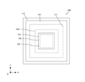
- FIG. 1 is a plan view showing a configuration example of an image sensor 100 according to a first embodiment of the present disclosure. It is a figure showing an example of a manufacturing method of electromagnetic shield 140 concerning a 1st embodiment of this indication. It is a figure showing an example of a manufacturing method of image pick-up element 100 concerning a 1st embodiment of this indication. It is sectional drawing which shows the structural example of the image sensor 500 which concerns on a comparative example.
- FIG. 4 is a cross-sectional view showing a configuration example of an image sensor 200 according to a second embodiment of the present disclosure.
- FIG. 1 is a plan view showing a configuration example of an image sensor 100 according to a first embodiment of the present disclosure. It is a figure showing an example of a manufacturing method of electromagnetic shield 140 concerning a 1st embodiment of this indication. It is a figure showing an example of a manufacturing method of image pick
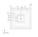
- FIG. 5 is a plan view showing a configuration example of an image sensor 200 according to a second embodiment of the present disclosure. It is a figure which shows an example of the manufacturing method of the electromagnetic shield 240 which concerns on the 2nd Embodiment of this indication.
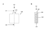
- FIG. 6 is a plan view and a cross-sectional view showing a configuration example of an electromagnetic shield 240 according to a second embodiment of the present disclosure. It is a figure which shows an example of the manufacturing method of the image pick-up element 200 which concerns on the 2nd Embodiment of this indication. It is a top view showing the example of composition of the electromagnetic shield concerning the modification of a 2nd embodiment of this indication. It is a block diagram showing an example of schematic composition of a camera which is an example of an imaging device to which this indication can be applied.
- FIG. 1 is a cross-sectional view showing a configuration example of an image sensor 100 according to the first embodiment of the present disclosure.
- FIG. 2 is a plan view showing a configuration example of the image sensor 100 according to the first embodiment of the present disclosure.
- the X direction, the Y direction, and the Z direction are three directions orthogonal to each other.
- the image pickup device 100 has a package 110, an image pickup chip 120, a seal glass 130, an electromagnetic shield 140, a die bond resin 150, bonding wires 160a and 160b, and inner leads 161a and 161b.
- the package 110 has a recess 111, and the imaging chip 120 is housed in the recess 111.
- the recess 111 is formed in the package 110 so as to be deeper than the thickness (distance in the Z direction) of the imaging chip 120 and the die bond resin 150.
- a material having an insulating property can be used as the material of the package 110.
- the package 110 may be made of a material such as synthetic resin or ceramic.
- the package 110 may be a stacked type package such as LTCC (Low Temperature Co-fired Ceramics) and HTCC (High Temperature Co-fired Ceramics). Further, inside the package 110, package wirings 112a to 112c are provided. The package wirings 112a to 112c can be provided between the layers included in the package 110.
- LTCC Low Temperature Co-fired Ceramics
- HTCC High Temperature Co-fired Ceramics
- the package wirings 112a to 112c electrically connect an external terminal (not shown) provided in the package 110 and the imaging chip 120.
- the package wirings 112a to 112c are electrically connected to the imaging chip 120 by, for example, bonding wires 160a and 160b. Further, an inner lead 161a to which the bonding wire 160a is connected and an inner lead 161b to which the bonding wire 160b is connected are formed in the recess 111 of the package 110.
- As the material of the package wirings 112a to 112c for example, tungsten, copper or the like can be used.
- the imaging chip 120 is a semiconductor chip that receives light emitted to a pixel region 121 (light receiving surface) via an optical system (not shown) and outputs an image signal according to the amount of light received by each pixel. Is.
- the imaging chip 120 has, for example, a signal processing area and a circuit area arranged around the signal processing area.
- the signal processing region includes a pixel region 121 (light receiving surface) in which a plurality of photodiodes that convert light into an electric signal are arranged one-dimensionally or two-dimensionally, and an amplifier circuit arranged in the periphery of the pixel region 121. It has a memory and so on.
- the image pickup chip 120 is mounted on the upper side (the upper side in the Z direction) of the electromagnetic shield 140 adhered to the die attach surface of the recess 111 of the package 110 by using the die bond resin 150.
- the image sensor for example, a CCD (Charge Coupled Device) or a CMOS (Complementary Metal Oxide Semiconductor) sensor can be used.
- the seal glass 130 is fixed to the package 110 so as to cover the pixel region 121 (light receiving surface) of the imaging chip 120, and hermetically seals the space 113 in which the imaging chip 120 is arranged.
- the seal glass 130 is bonded to the package 110 with an adhesive or the like, and closes the recess 111 of the package 110.
- the seal glass 130 is light transmissive and has a function of preventing scratches, dust, and the like from adhering to the imaging chip 120.
- the material of the seal glass 130 for example, borosilicate glass, quartz glass, non-alkali glass, Pyrex (registered trademark) or the like can be used.
- an IR (infrared) cut filter that blocks infrared light, a crystal low-pass filter, or the like may be used.
- the electromagnetic shield 140 is an electromagnetic shield (magnetic shield or electrostatic shield) produced by laminating the adhesive films 142 and 143 on both surfaces of the metal film 141, and is adhered to the die attach surface of the recess 111 of the package 110.
- the imaging chip 120 is mounted on the upper side of the electromagnetic shield 140 (the upper side in the Z direction) using the die bond resin 150.
- noise for example, band-shaped noise
- the electromagnetic shield 140 is arranged between the imaging chip 120 and the package wirings 112a to 112c (package 110). As a result, noise (for example, band-shaped noise) generated by magnetism from the package wirings 112a to 112c can be suppressed, and characteristic deterioration of the imaging chip 120 can be prevented.
- the size of the electromagnetic shield 140 is made smaller than the size of the imaging chip 120 in a top view (when viewed from the upper side in the Z direction). That is, the rectangular area of the electromagnetic shield 140 is made smaller than the rectangular area of the imaging chip 120 in a top view.
- the size of the electromagnetic shield 140 can be substantially the same as the size of the pixel region 121 (smaller than the size of the imaging chip 120) in a top view.
- the electromagnetic shield 140 can be configured to have a total thickness (thickness (distance in the Z direction)) of 100 ⁇ m or less. This makes it possible to reduce the height of the imaging chip 120 arranged on the die attach surface while maintaining the shield effect.
- a conductor such as a magnetic film, copper (for example, copper foil), or aluminum can be used. It is preferable that the metal film 141 is made of a material having high conductivity such as copper. This is because the electrostatic shield effect in the electromagnetic shield 140 can be improved.
- the relative magnetic permeability at 100 kHz is 1000 or more, and further, the relative magnetic permeability at 100 kHz is 5000. The above is preferable. This is because the magnetic shield effect of the electromagnetic shield 140 can be improved. A method of manufacturing the electromagnetic shield 140 will be described in detail with reference to FIG.
- the die bond resin 150 is an adhesive agent for die bonding used to mount the imaging chip 120 in the recess 111 of the package 110. Specifically, the die bond resin 150 is used to mount the imaging chip 120 on the upper side (the upper side in the Z direction) of the electromagnetic shield 140 bonded to the die attach surface of the recess 111 of the package 110. The die bond resin 150 is applied so as to cover the side surface of the electromagnetic shield 140. That is, the die bond resin 150 is applied so as to cover (protect) the metal film 141 located on the side surface of the electromagnetic shield 140 with the die bond resin 150. In this way, the die bond resin 150 is arranged in a square shape so as to cover only the outer peripheral portion of the electromagnetic shield 140.
- the die bond resin 150 is an example of the adhesive described in the claims.
- FIG. 3 is a diagram showing an example of a method for manufacturing the electromagnetic shield 140 according to the first embodiment of the present disclosure.
- FIG. 3A shows a top view of a large area electromagnetic shield formed by laminating a large area adhesive film on both sides of a large area metal film.
- FIG. 3B is a side view of the electromagnetic shield when the large-area electromagnetic shield shown in FIG. 3A is cut by the cutting members 171 to 173. Note that FIG. 3 shows an example in which a large-area electromagnetic shield is cut into six electromagnetic shields for ease of explanation, but the present invention is not limited to this.
- a dotted line shows a portion for cutting a large-area electromagnetic shield formed by laminating a large-area adhesive film on both sides of a large-area metal film.
- FIG. 3B shows the side surface of the large-area electromagnetic shield when viewed from the direction of arrow 170 shown in FIG. 3A.
- the large-area electromagnetic shield is formed by laminating adhesive films 182 and 183 having the same size (or substantially the same size) as the size of the metal film 181 on both surfaces of the large-area metal film 181. .. Then, the electromagnetic shield 140 is produced by cutting the large-area electromagnetic shield formed by the large-area metal film 181, the large-area adhesive films 182, and 183 to a desired size with the cutting members 171 to 173.
- the large-area electromagnetic shield formed by laminating the large-area adhesive films 182 and 183 on both surfaces of the large-area metal film 181 is cut to cut the image pickup device 100.
- the electromagnetic shield 140 used in the above can be manufactured. Therefore, the productivity of the electromagnetic shield 140 can be improved, and the manufacturing cost of the image sensor 100 can be reduced.
- FIG. 4 is a diagram showing an example of a method for manufacturing the image sensor 100 according to the first embodiment of the present disclosure.
- the electromagnetic shield 140 formed by laminating the adhesive films 142 and 143 on both surfaces of the metal film 141 is adhered to the die attach surface of the recess 111 of the package 110.
- the die bond resin 150 covers the side surface (the surface where the metal film 141 is exposed) of the outer periphery of the electromagnetic shield 140 adhered to the die attach surface of the recess 111 of the package 110. Apply. That is, the die bond resin 150 is applied in a square shape so as to cover the side surface of the outer peripheral portion of the electromagnetic shield 140. As a result, the metal film 141 located on the side surface of the electromagnetic shield 140 is protected by the die bond resin 150.
- the imaging chip 120 is placed on the die bond resin 150 applied to the side surface of the outer peripheral portion of the electromagnetic shield 140 adhered to the die attach surface of the recess 111 of the package 110. After mounting the imaging chip 120, the die bond resin 150 is cured. After that, wire bonding is performed, and the package wirings 112a to 112c of the package 110 and the imaging chip 120 are electrically connected by the bonding wires 160a and 160b.
- the seal glass 130 is fixed to the package 110 to hermetically seal the space 113 in which the imaging chip 120 is arranged.
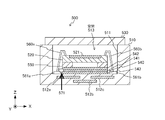
- FIG. 5 is a cross-sectional view showing a configuration example of the image sensor 500 according to the comparative example.
- the image pickup device 500 has a package 510, an image pickup chip 520, a seal glass 530, an electromagnetic shield 540, a die bond resin 550, bonding wires 560a and 560b, and inner leads 561a and 561b.
- Each part of the image sensor 500 corresponds to each part of the same name in the image sensor 100 shown in FIG. However, while the die bond resin 150 in the image pickup device 100 is applied so as to cover the side surface of the electromagnetic shield 140, the die bond resin 550 in the image pickup device 500 is applied on the upper side of the electromagnetic shield 540. That is, the electromagnetic shield 540 is installed on the die attach surface of the recess 511 of the package 510 with the metal film 541 on the side surface exposed.
- the image sensor 500 is subjected to a high temperature and high humidity test.
- the electromagnetic shield 540 since the electromagnetic shield 540 is installed in the recess 511 of the package 510 with the metal film 541 exposed on the side surface of the electromagnetic shield 540, the metal film 541 may be eluted by the high temperature and high humidity test.
- a short circuit may occur between the eluted metal film 541 and the inner lead 561a of the package 510, as indicated by an arrow 571.
- the side surface of the electromagnetic shield 140 is covered with the die bond resin 150 so that the metal film 141 is protected.
- the electromagnetic shield 140 is installed in the recess 111 of the package 110 in a state where the metal film 141 on the side surface of the electromagnetic shield 140 is protected, so that the metal film 141 is prevented from being eluted by the high temperature and high humidity test. be able to. Accordingly, it is possible to prevent the occurrence of a short circuit between the metal film 141 and the inner leads 161a and 161b of the package 110.
- the die bond resin 150 is arranged in a square shape so as to cover only the outer peripheral portion of the electromagnetic shield 140.
- the die bond resin 150 may be applied and arranged so as to cover the entire top surface and side surfaces of the electromagnetic shield 140.
- the side surface of the electromagnetic shield 140 disposed on the bottom surface of the image pickup chip 120 is covered with the die bond resin 150 adhesive, so that the electromagnetic shield 140 is formed. A short circuit with another conductor can be prevented.
- Second Embodiment> In the first embodiment, the example in which the die bond resin 150 is applied so as to cover the side surface of the electromagnetic shield 140 provided on the die attach surface of the recess 111 of the package 110 has been shown. As described above, when the die-bonding resin 150 is applied in a square shape, the space surrounded by the imaging chip 120, the die-bonding resin 150, and the electromagnetic shield 140 is sealed. Therefore, it is conceivable to provide air holes in the space in consideration of the fact that the pressure in the space becomes high.
- an example is shown in which a part of the square-shaped die-bonding resin is used as a slit, and an air hole is provided in a space surrounded by the imaging chip, the die-bonding resin, and the electromagnetic shield.
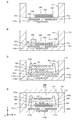
- FIG. 6 is a cross-sectional view showing a configuration example of the image sensor 200 according to the second embodiment of the present disclosure.
- FIG. 7 is a plan view showing a configuration example of the image sensor 200 according to the second embodiment of the present disclosure.
- the image pickup device 200 is different from the image pickup device 100 shown in FIGS. 1 and 2 in that an electromagnetic shield 240 having a covering end 245 is provided in place of the electromagnetic shield 140, and a die bond resin 250 is provided at a portion corresponding to the covering end 245. It is different from the image sensor 100 in that it is not applied. Note that, except for these points, the image sensor 100 is the same as the image sensor 100 shown in FIGS. 1 and 2, and therefore, the same parts as those of the image sensor 100 are designated by the same reference numerals and the description thereof will be omitted. Further, the covered end portion 245 will be described in detail with reference to FIGS. 8 and 9.
- FIG. 8 is a diagram showing an example of a method for manufacturing the electromagnetic shield 240 according to the second embodiment of the present disclosure.
- FIG. 9 is a plan view and a cross-sectional view showing a configuration example of the electromagnetic shield 240 according to the second embodiment of the present disclosure.
- FIG. 8A shows a top view of a large-area adhesive film that constitutes a large-area electromagnetic shield.
- FIG. 8B shows a top view of a large-area metal film forming a large-area electromagnetic shield.
- a portion for cutting the large-area adhesive film and the large-area metal film is shown by a dotted line. Note that, in FIG. 8, an example in which a large-area electromagnetic shield is cut into six electromagnetic shields for ease of explanation, but the present invention is not limited to this.
- the large-area metal film is manufactured in a roll shape (strip shape) with the width L1 narrower than the width L3 of the large-area adhesive film.
- the length L2 of the large area metal film may be the same (or substantially the same) as the length L2 of the large area adhesive film.
- the large-area adhesive film is cut so as to provide the coated ends (metal film-less portion, protrusion) 245 at both ends (both ends in the width direction) of the roll (band).
- the electromagnetic shield 240 having the coated end portion 245 is manufactured, it is formed by laminating the large area adhesive film shown in FIG. 8A on both surfaces of the large area metal film shown in FIG. 8B.
- Use an area electromagnetic shield In other words, the horizontal direction (the horizontal direction shown in FIG. 8) is significantly longer than the vertical direction (the vertical direction shown in FIG. 8), and there is no metal film at both ends in the vertical direction, and only the adhesive film exists.
- a roll-shaped roll having a peripheral portion portion including the coated end portion
- the peripheral portion corresponds to one side of the electromagnetic shield 240, and the peripheral portion is cut out so as to have the shape of the covered end portion 245.
- FIG. 9 shows the electromagnetic shield 240 formed by the adhesive film thus cut so as to provide the covered end 245 and the metal film cut without the covered end.
- FIG. 9A shows a plan view of an electromagnetic shield 240 formed by laminating an adhesive film having a coated end 245 on both surfaces of a metal film having no coated end.
- FIG. 9B shows a cross-sectional view of the electromagnetic shield 240 when viewed from the directions of arrows A1 and A2 in FIG. 9A.
- the adhesive film has a coated end 245, but the metal film does not have a coated end. Therefore, as shown in FIG. 9B, the layer of the metal film 241 is not formed on the coated end portion 245, and the metal film 241 is not exposed on the side surface of the coated end portion 245 of the electromagnetic shield 240. As described above, of the side surfaces of the metal film 241 in the electromagnetic shield 240, the portion corresponding to the coated end portion 245 of the electromagnetic shield 240 is protected by the adhesive films 242 formed on both surfaces of the metal film 241.
- the side surface of the tip end of the coated end 245 of the electromagnetic shield 240 the side surface of the metal film 241 is protected by the adhesive film 242 forming the coated end 245, and the metal film 241 is exposed. do not do.
- the coated end portion 245 of the electromagnetic shield 240 needs to be protected by the die bond resin 250 because the side surface of the metal film 241 is protected by the adhesive film 242 forming the coated end portion 245 and the metal film 241 is not exposed. There is no. Therefore, when the die bond resin 250 is applied to the side surface of the electromagnetic shield 240, the die bond resin 250 is not applied to the portion corresponding to the covering end portion 245 as shown in FIGS. 6 and 7. That is, the die bond resin 250 can be applied so that the coated end portion 245 becomes a slit of the die bond resin 250.
- the die bond resin 250 is arranged in a square shape so as to cover only the outer peripheral portion (outer surface) of the electromagnetic shield 240, and a slit is formed in at least one place of the square shape. Further, the coated end portion 245 of the electromagnetic shield 240 is arranged in the slit. Further, as shown in FIGS. 6 and 7, in the slit, a hole 243 can be formed on the upper side (the upper side in the Z direction) of the covering end 245. ..
- FIG. 10 is a diagram showing an example of a method for manufacturing the image sensor 200 according to the second embodiment of the present disclosure.
- the electromagnetic shield 240 formed by laminating the adhesive films 242 on both surfaces of the metal film 241 is bonded to the die attach surface of the recess 111 of the package 110.
- the coated end 245 of the electromagnetic shield 240 the side surface of the metal film 241 is protected by the adhesive film 242 forming the coated end 245.
- the side surface of the outer peripheral portion of the electromagnetic shield 240 adhered to the die attach surface of the recess 111 of the package 110 (the side surface other than the side surface of the tip of the covered end 245 of the electromagnetic shield 240) is covered.
- the die bond resin 250 is applied. That is, the die-bonding resin 250 is applied in a square shape so as to cover the side surface of the outer peripheral portion of the electromagnetic shield 240, but the die-bonding resin 250 is chipped only at the covered end portion 245 of the electromagnetic shield 240.
- the die-bonding resin 250 is applied in a square shape so as to cover the side surface of the outer peripheral portion of the electromagnetic shield 240, and a slit is formed in at least one portion of the square shape (the position of the covered end portion 245 of the electromagnetic shield 240). To be done. As described above, by forming the slits in at least one place of the die-bonding resin 250 applied in the square shape, the hole 243 is formed on the upper side (the upper side in the Z direction) of the covering end 245. This can prevent the space surrounded by the imaging chip 120, the die bond resin 250, and the electromagnetic shield 240 from being hermetically sealed. When the heat treatment is performed to cure the adhesive or the like, it is possible to prevent the imaging chip 120 from floating or being damaged due to an increase in pressure in the space.
- the metal film 241 exposed on the side surface of the electromagnetic shield 240 is protected by the die bond resin 250. Further, the coated end portion 245 of the electromagnetic shield 240 is disposed in the slit portion where the die bond resin 250 is lacking, but the metal film 241 is not exposed on the side surface of the coated end portion 245. The metal film 241 near the coated end 245 of the electromagnetic shield 240 is protected by the adhesive film 242 forming the coated end 245.
- the imaging chip 120 is placed on the die bond resin 250 applied to the side surface of the outer peripheral portion of the electromagnetic shield 240 adhered to the die attach surface of the recess 111 of the package 110.
- the die bond resin 250 is cured, and the package wirings 112a to 112c of the package 110 and the image pickup chip 120 are electrically connected by the bonding wires 160a and 160b.
- the seal glass 130 is fixed to the package 110 to hermetically seal the space 113 in which the imaging chip 120 is arranged.
- the image sensor 200 according to the second embodiment of the present disclosure can simplify the manufacturing process of the electromagnetic shield 240 by using the electromagnetic shield 240 including the clothing end 245. Further, by omitting the die-bonding resin 250 on the clothing end portion 245, it is possible to prevent damage or the like of the imaging chip 120 in the manufacturing process of the imaging element 200.
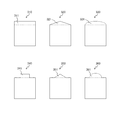
- FIG. 11 is a plan view showing a configuration example of an electromagnetic shield according to a modified example of the second embodiment of the present disclosure.
- the electromagnetic shields 310, 320, 330, 340, 350, and 360 are modifications of the electromagnetic shield 240, and the shape of the coated end portion is different from that of the electromagnetic shield 240. Therefore, here, the shape of the coated end portion will be mainly described.
- FIG. 11 a rectangular electromagnetic shield formed by laminating adhesive films on both surfaces of a metal film, and covering end portions 311, 321, 331, 341, 351 and 361 formed of only the adhesive film are shown. The boundaries are indicated by dotted lines.
- the electromagnetic shield 310 has a rectangular coated end 311 provided on one side of a rectangle of the electromagnetic shield 310 (a rectangle formed by laminating adhesive films on both surfaces of a metal film). That is, in the electromagnetic shield 310, one side of the rectangle of the electromagnetic shield 310 becomes one rectangular covered end portion 311.
- the electromagnetic shield 320 is provided with a triangular covered end 321 on one side of a rectangle (a rectangle formed by laminating adhesive films on both surfaces of a metal film) of the electromagnetic shield 320. That is, the electromagnetic shield 320 is one in which one side of the rectangle of the electromagnetic shield 320 is one covered end 321 having a triangular shape.
- the electromagnetic shield 330 is one in which an arc-shaped covered end 331 is provided on one side of a rectangle of the electromagnetic shield 330 (a rectangle formed by laminating adhesive films on both surfaces of a metal film). That is, in the electromagnetic shield 330, one side of the rectangle of the electromagnetic shield 330 becomes one arcuate covering end 331.
- the electromagnetic shield 340 has a rectangular coated end 341 provided on one side of a rectangle of the electromagnetic shield 340 (a rectangle formed by laminating adhesive films on both surfaces of a metal film). That is, the electromagnetic shield 340 is provided with the rectangular covered end 341 only on a part of one side of the rectangle of the electromagnetic shield 340. Note that the electromagnetic shield 340 is obtained by changing only the length of the electromagnetic shield 240 shown in FIG. 9 in the left-right direction (left-right direction in FIG. 11).
- the electromagnetic shield 350 is provided with a triangular covered end 351 on one side of a rectangle of the electromagnetic shield 350 (a rectangle formed by laminating adhesive films on both surfaces of a metal film). That is, the electromagnetic shield 350 is provided with the triangular covered end 351 only on a part of one side of the rectangle of the electromagnetic shield 350.
- the electromagnetic shield 360 is one in which an arc-shaped coated end 361 is provided on one side of a rectangle of the electromagnetic shield 360 (a rectangle formed by laminating adhesive films on both sides of a metal film). That is, the electromagnetic shield 360 is provided with the arcuate covering end 361 only on a part of one side of the rectangle of the electromagnetic shield 360.
- the technology according to the present disclosure (this technology) can be applied to various products.
- the present technology may be realized as an image pickup device mounted in an image pickup apparatus such as a camera.
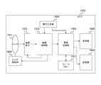
- FIG. 12 is a block diagram showing a schematic configuration example of a camera which is an example of an imaging device to which the present technology can be applied.
- the camera 1000 in the figure includes a lens 1001, an image sensor 1002, an imaging control unit 1003, a lens driving unit 1004, an image processing unit 1005, an operation input unit 1006, a frame memory 1007, and a display unit 1008. And a recording unit 1009. ..
- the lens 1001 is a taking lens of the camera 1000.
- the lens 1001 collects light from a subject and makes it incident on an image sensor 1002 described later to form an image of the subject.
- the image pickup element 1002 is a semiconductor element that picks up light from a subject condensed by the lens 1001.
- the image sensor 1002 generates an analog image signal according to the emitted light, converts it into a digital image signal, and outputs it.
- the image capturing control unit 1003 controls image capturing by the image sensor 1002.
- the imaging control unit 1003 controls the imaging element 1002 by generating a control signal and outputting the control signal to the imaging element 1002.
- the imaging control unit 1003 can also perform autofocus in the camera 1000 based on the image signal output from the image sensor 1002.
- the auto focus is a system that detects the focal position of the lens 1001 and automatically adjusts it.
- a method (image plane phase difference autofocus) of detecting a focus position by detecting an image plane phase difference by a phase difference pixel arranged in the image sensor 1002 can be used. It is also possible to apply a method (contrast autofocus) of detecting the position where the contrast of the image is the highest as the focus position.
- the imaging control unit 1003 adjusts the position of the lens 1001 via the lens driving unit 1004 based on the detected focus position, and performs autofocus.
- the imaging control unit 1003 can be configured by, for example, a DSP (Digital Signal Processor) equipped with firmware.
- DSP Digital Signal Processor
- the lens driving unit 1004 drives the lens 1001 under the control of the imaging control unit 1003.
- the lens driving unit 1004 can drive the lens 1001 by changing the position of the lens 1001 using a built-in motor.
- the image processing unit 1005 processes the image signal generated by the image sensor 1002. This processing includes, for example, demosaic for generating image signals of insufficient colors among the image signals corresponding to red, green and blue for each pixel, noise reduction for removing noise of the image signals and encoding of the image signals. Applicable
- the image processing unit 1005 can be configured by, for example, a microcomputer equipped with firmware.
- the operation input unit 1006 receives an operation input from the user of the camera 1000.
- this operation input unit 1006 for example, a push button or a touch panel can be used.
- the operation input received by the operation input unit 1006 is transmitted to the imaging control unit 1003 and the image processing unit 1005. After that, a process according to the operation input, for example, a process of capturing an image of a subject is started.
- the frame memory 1007 is a memory that stores a frame that is an image signal for one screen.
- the frame memory 1007 is controlled by the image processing unit 1005 and holds frames in the process of image processing.
- the display unit 1008 displays the image processed by the image processing unit 1005.
- a liquid crystal panel can be used for the display unit 1008.
- the recording unit 1009 records the image processed by the image processing unit 1005.
- a memory card or a hard disk can be used.
- the present technology can be applied to the image sensor 1002 among the configurations described above.
- the image pickup devices 100 and 200 described with reference to FIGS. 1, 2, 6, and 7 can be applied to the image pickup device 1002.
- the productivity of the electromagnetic shield included in the image pickup device 1002 can be increased, and the manufacturing cost of the camera 1000 can be reduced.
- the image pickup devices 100 and 200 to the image pickup device 1002 it is possible to prevent a short circuit from occurring in the recess of the package of the image pickup device 1002.
- the image processing unit 1005 is an example of the processing circuit described in the claims.
- the camera 1000 is an example of the imaging device described in the claims.
- the camera has been described as an example, but the technique according to the present invention may be applied to other devices such as a monitoring device.
- drawings in the above-described embodiments are schematic, and the dimensional ratios of the respective parts and the like do not necessarily match the actual ones. Moreover, it is needless to say that the drawings may include portions having different dimensional relationships and ratios.
- the present technology may have the following configurations.
- (1) In a package including wiring inside and provided with a recess for mounting an image pickup chip, an electromagnetic shield arranged between the wiring and the image pickup chip, An image pickup device comprising: an adhesive used to mount the image pickup chip, the adhesive being arranged so as to cover the electromagnetic shield.
- (2) The image pickup device according to (1), wherein the adhesive is arranged so as to cover all of the electromagnetic shield.
- (3) The image pickup device according to (1) or (2), wherein the adhesive is arranged so as to cover the entire outer surface of the electromagnetic shield.
- (4) The image pickup device according to any one of (1) to (3), wherein the electromagnetic shield is formed by laminating an adhesive film on both surfaces of a metal film.
- the imaging chip has a substantially rectangular shape in a top view
- the electromagnetic shield has a substantially rectangular shape in a top view
- the adhesive is arranged in a square shape in a top view so as to cover the entire outer surface of the electromagnetic shield,
- the image pickup device according to any one of (1) to (5), wherein the image pickup chip is mounted on an upper side of the adhesive arranged in the square shape.
- the electromagnetic shield is formed by laminating an adhesive film on both sides of a metal film in a substantially rectangular portion in a top view, and is formed of only the adhesive film in a portion corresponding to one side of the approximately rectangular shape.
- the imaging chip has a substantially rectangular shape in a top view, The adhesive is arranged in a substantially square V shape in which a portion corresponding to the covering end portion is cut off in a top view, and the imaging chip is arranged above the adhesive arranged in the substantially square V shape.
- the image pickup device according to (7) which is mounted.
- the image pickup device according to any one of (1) to (9), wherein the size of the electromagnetic shield is substantially the same as the size of the light receiving surface of the image pickup chip in a top view.
- the metal film is a soft magnetic material having a relative magnetic permeability of 100 or more at 1000 kHz.
- the image pickup device according to (11), wherein the metal film has a relative magnetic permeability of 5000 or more at 100 kHz.
- the image pickup device according to any one of (1) to (13), wherein the electromagnetic shield is a magnetic shield or an electrostatic shield.
- An image pickup device comprising an adhesive used and an adhesive arranged to cover the electromagnetic shield,
- An image pickup apparatus comprising: a processing circuit that processes an image signal generated by the image pickup element.
Landscapes
- Engineering & Computer Science (AREA)
- Multimedia (AREA)
- Signal Processing (AREA)
- Physics & Mathematics (AREA)
- Electromagnetism (AREA)
- Solid State Image Pick-Up Elements (AREA)
- Transforming Light Signals Into Electric Signals (AREA)
Abstract
電磁シールドが配置された撮像素子におけるショートを防止する。 撮像素子は、電磁シールドと、接着剤とを具備する撮像素子である。電磁シールドは、内部に配線を備え、撮像チップを搭載するための凹部が設けられているパッケージにおいて、配線と撮像チップとの間に配置される電磁シールドである。また、接着剤は、撮像チップを搭載するために用いる接着剤である。また、接着剤は、電磁シールドを覆うように配置される。
Description
本開示は、撮像素子および撮像装置に関する。詳しくは、パッケージ内に撮像チップが搭載される撮像素子およびこれを備える撮像装置に関する。
従来、被写体を撮像して画像データを生成するデジタルスチルカメラ、デジタルビデオカメラ(例えば、カメラ一体型レコーダ)、監視カメラ等の撮像装置が普及している。また、これらの撮像装置に備えられる撮像素子として、例えば、撮像チップが搭載されたパッケージの内部に配線が設けられている撮像素子が存在する。しかし、近年では、大電流を流す仕様が増えているため、パッケージの内部に設けられている配線からの磁力線の影響による撮像素子の特性劣化を防止することが重要となる。
そこで、例えば、パッケージの内部に備える配線とパッケージの凹部に収容される撮像チップとの間に、配線において生じる磁力線の撮像チップへの到達を防止するシールドを配置する撮像素子が提案されている(例えば、特許文献1参照。)。
上述の従来技術では、パッケージの内部に備える配線において生じる磁力線の撮像チップへの到達を防止することができる。ここで、パッケージの内部に備える配線と撮像チップとを電気的に接続するボンディングワイヤやインナーリード等がパッケージの凹部に設けられることもある。この場合には、上述のシールドが磁性体や導電体であるため、パッケージの凹部におけるシールドとインナーリード等とのショートを防止することが重要となる。
本開示は、上述した問題点に鑑みてなされたものであり、シールドが配置された撮像素子におけるショートを防止することを目的としている。
本開示の第1の態様は、内部に配線を備え、撮像チップを搭載するための凹部が設けられているパッケージにおいて、前記配線と前記撮像チップとの間に配置される電磁シールドと、前記撮像チップを搭載するために用いる接着剤であって前記電磁シールドを覆うように配置される接着剤とを具備する撮像素子である。
また、この第1の態様において、前記接着剤は、前記電磁シールドの全てを覆うように配置されてもよい。
また、この第1の態様において、前記接着剤は、前記電磁シールドの外側面の全てを覆うように配置されてもよい。
また、この第1の態様において、前記電磁シールドは、金属膜の両面に接着フィルムをラミネートして形成されてもよい。
また、この第1の態様において、前記接着剤は、前記電磁シールドの外側面に露出される前記金属膜の全てを覆うように配置されてもよい。
また、この第1の態様において、前記撮像チップは、上面視において略矩形状であり、前記電磁シールドは、上面視において略矩形状であり、前記接着剤は、前記電磁シールドの外側面の全てを覆うように、上面視においてロの字形状に配置され、前記撮像チップは、前記ロの字形状に配置される前記接着剤の上側に搭載されてもよい。
また、この第1の態様において、前記電磁シールドは、上面視において略矩形状となる部分が金属膜の両面に接着フィルムをラミネートして形成され、前記略矩形状の一辺に相当する部分に、前記接着フィルムのみで形成される被覆端部を備え、前記接着剤は、前記電磁シールドの外側面に露出される前記金属膜の全てを覆うように配置されてもよい。
また、この第1の態様において、前記撮像チップは、上面視において略矩形状であり、前記接着剤は、上面視において前記被覆端部に相当する部分が欠けている略ロの字形状に配置され、前記撮像チップは、前記略ロの字形状に配置される前記接着剤の上側に搭載されてもよい。
また、この第1の態様において、上面視において前記電磁シールドのサイズを、前記撮像チップのサイズよりも小さくしてもよい。
また、この第1の態様において、上面視において前記電磁シールドのサイズを、前記撮像チップの受光面のサイズと略同一としてもよい。
また、この第1の態様において、前記金属膜を、100kHzの比透磁率が1000以上である軟磁性体としてもよい。
また、この第1の態様において、前記金属膜を、100kHzの比透磁率が5000以上としてもよい。
また、この第1の態様において、前記金属膜を、銅またはアルミニウムとしてもよい。
また、この第1の態様において、前記電磁シールドを、磁気シールドまたは静電シールドとしてもよい。
また、本開示の第2の態様は、内部に配線を備え、撮像チップを搭載するための凹部が設けられているパッケージにおいて、前記配線と前記撮像チップとの間に配置される電磁シールドと、前記撮像チップを搭載するために用いる接着剤であって前記電磁シールドを覆うように配置される接着剤とを備える撮像素子と、前記撮像素子により生成された画像信号を処理する処理回路とを具備する撮像装置である。
このような態様を採ることにより、パッケージの凹部において、電磁シールを接着剤で覆うことにより電磁シールドと他の導電体との間でのショートの発生を防止するという作用をもたらす。
次に、図面を参照して、本開示を実施するための形態(以下、実施の形態と称する)を説明する。以下の図面において、同一または類似の部分には同一または類似の符号を付している。また、以下の順序で実施の形態の説明を行う。
1.第1の実施の形態
2.第2の実施の形態
3.変形例
4.カメラへの応用例
1.第1の実施の形態
2.第2の実施の形態
3.変形例
4.カメラへの応用例
<1.第1の実施の形態>
[撮像素子の構成]
図1は、本開示の第1の実施の形態に係る撮像素子100の構成例を示す断面図である。図2は、本開示の第1の実施の形態に係る撮像素子100の構成例を示す平面図である。なお、以下の各図において、X方向、Y方向およびZ方向は相互に直交する3方向である。
[撮像素子の構成]
図1は、本開示の第1の実施の形態に係る撮像素子100の構成例を示す断面図である。図2は、本開示の第1の実施の形態に係る撮像素子100の構成例を示す平面図である。なお、以下の各図において、X方向、Y方向およびZ方向は相互に直交する3方向である。
撮像素子100は、パッケージ110と、撮像チップ120と、シールガラス130と、電磁シールド140と、ダイボンド樹脂150と、ボンディングワイヤ160aおよび160bと、インナーリード161aおよび161bとを有する。
パッケージ110は、凹部111を有し、凹部111に撮像チップ120を収容するものである。凹部111は、撮像チップ120およびダイボンド樹脂150の厚み(Z方向の距離)よりも深くなるようにパッケージ110に形成される。なお、パッケージ110の材料として、絶縁性を有する材料を用いることができる。例えば、合成樹脂やセラミック等の材料からなるものをパッケージ110の材料とすることができる。
また、パッケージ110は、例えば、LTCC(Low Temperature Co-fired Ceramics)、HTCC(High Temperature Co-fired Ceramics)等の積層型のパッケージとすることができる。また、パッケージ110の内部には、パッケージ配線112a乃至cが設けられている。パッケージ配線112a乃至cは、パッケージ110を構成する各層の間に設けることができる。
パッケージ配線112a乃至cは、パッケージ110に設けられている外部端子(図示を省略)と、撮像チップ120とを電気的に接続する。また、パッケージ配線112a乃至cは、例えば、ボンディングワイヤ160aおよび160bにより撮像チップ120と電気的に接続されている。また、パッケージ110の凹部111には、ボンディングワイヤ160aが接続されるインナーリード161aと、ボンディングワイヤ160bが接続されるインナーリード161bとが形成される。なお、パッケージ配線112a乃至cの材料として、例えば、タングステンおよび銅等を用いることができる。
撮像チップ120は、光学系(図示を省略)を介して画素領域121(受光面)に照射される光を受光して、各画素が光を受光した光量に応じた画像信号を出力する半導体チップである。撮像チップ120は、例えば、信号処理領域と、当該信号処理領域の周辺に配置された回路領域とを有する。信号処理領域は、光を電気信号に変換する複数のフォトダイオードが一次元または二次元的に配置されている画素領域121(受光面)と、画素領域121の周辺に配置されている増幅回路やメモリ等を有する。また、撮像チップ120は、パッケージ110の凹部111のダイアタッチ面に接着される電磁シールド140の上側(Z方向の上側)に、ダイボンド樹脂150を用いて搭載される。なお、撮像素子として、例えば、CCD(Charge Coupled Device)やCMOS(Complementary Metal Oxide Semiconductor)センサ等を用いることができる。
シールガラス130は、撮像チップ120の画素領域121(受光面)を覆うように、パッケージ110に対して固定され、撮像チップ120が配置される空間113を気密封止するものである。例えば、シールガラス130は、接着剤等によりパッケージ110に接合され、パッケージ110の凹部111を閉塞する。また、シールガラス130は、光透過性を有し、撮像チップ120に傷や埃等が付着するのを防止する機能を有する。
シールガラス130の材料として、例えば、ホウケイ酸ガラス、石英ガラス、無アルカリガラス、パイレックス(登録商標)等を用いることができる。なお、シールガラス130の代わりに、赤外光を遮断するIR(infrared)カットフィルタや、水晶ローパスフィルタ等を用いるようにしてもよい。
電磁シールド140は、金属膜141の両面に接着フィルム142および143をラミネートして作製される電磁シールド(磁気シールドまたは静電シールド)であり、パッケージ110の凹部111のダイアタッチ面に接着される。また、電磁シールド140の上側(Z方向の上側)には、ダイボンド樹脂150を用いて撮像チップ120が搭載される。ここで、パッケージ110の内部に設けられているパッケージ配線112a乃至cからの磁気によりノイズ(例えば、帯状のノイズ)が発生するおそれがある。そこで、本開示では、撮像チップ120とパッケージ配線112a乃至c(パッケージ110)との間に電磁シールド140を配置する。これにより、パッケージ配線112a乃至cからの磁気により発生するノイズ(例えば、帯状のノイズ)を抑制し、撮像チップ120の特性劣化を防止することができる。
また、上面視(Z方向の上側から見た場合)において、電磁シールド140のサイズは、撮像チップ120のサイズよりも小さくなるようにする。すなわち、上面視において、電磁シールド140の矩形の面積を、撮像チップ120の矩形の面積よりも小さくなるようにする。例えば、図2に示すように、上面視において、電磁シールド140のサイズを、画素領域121のサイズ(撮像チップ120のサイズよりも小さいサイズ)と略同一とすることができる。
なお、電磁シールド140は、100um以下の総厚(厚み(Z方向の距離))に構成することができる。これにより、シールド効果を保ちながらダイアタッチ面に配置された撮像チップ120を低背化することができる。また、金属膜141の材料として、磁性体膜、銅(例えば、銅箔)、アルミニウム等の導電体を用いることができる。銅等の高い導電率を有する材料により金属膜141を構成すると好適である。電磁シールド140における静電シールド効果を向上させることができるためである。また、例えば、金属膜141の材料として、鉄を主成分とする軟磁性体を用いる場合には、100kHzの比透磁率が1000以上とすることが好ましく、さらには、100kHzの比透磁率が5000以上とすることが好ましい。電磁シールド140における磁気シールド効果を向上させることができるためである。なお、電磁シールド140の製造方法については、図3を参照して詳細に説明する。
ダイボンド樹脂150は、パッケージ110の凹部111に撮像チップ120を搭載するために用いられるダイボンディング用の接着剤である。具体的には、ダイボンド樹脂150は、パッケージ110の凹部111のダイアタッチ面に接着される電磁シールド140の上側(Z方向の上側)に、撮像チップ120を搭載するために用いられる。また、ダイボンド樹脂150は、電磁シールド140の側面を覆うように塗布される。すなわち、電磁シールド140の側面に位置する金属膜141をダイボンド樹脂150により覆うように(保護するように)、ダイボンド樹脂150が塗布される。このように、ダイボンド樹脂150は、電磁シールド140の外周部のみを覆うようにロの字形状に配置される。なお、ダイボンド樹脂150は、請求の範囲に記載の接着剤の一例である。
[電磁シールドの製造例]
図3は、本開示の第1の実施の形態に係る電磁シールド140の製造方法の一例を示す図である。図3Aには、大面積の金属膜の両面に大面積の接着フィルムをラミネートして形成される大面積の電磁シールドの上面図を示す。図3Bには、図3Aに示す大面積の電磁シールドを切断部材171乃至173で切断する場合の電磁シールドの側面図を示す。なお、図3では、説明を容易にするため、大面積の電磁シールドを6つの電磁シールドに切断する例を示すが、これに限定されるものではない。
図3は、本開示の第1の実施の形態に係る電磁シールド140の製造方法の一例を示す図である。図3Aには、大面積の金属膜の両面に大面積の接着フィルムをラミネートして形成される大面積の電磁シールドの上面図を示す。図3Bには、図3Aに示す大面積の電磁シールドを切断部材171乃至173で切断する場合の電磁シールドの側面図を示す。なお、図3では、説明を容易にするため、大面積の電磁シールドを6つの電磁シールドに切断する例を示すが、これに限定されるものではない。
図3Aには、大面積の金属膜の両面に大面積の接着フィルムをラミネートして形成される大面積の電磁シールドを切断する部分を点線で示す。
図3Bには、図3Aに示す矢印170の方向から見た場合の大面積の電磁シールドの側面を示す。図3Bに示すように、大面積の電磁シールドは、大面積の金属膜181の両面に、金属膜181のサイズと同一(または略同一)サイズの接着フィルム182および183をラミネートして形成される。そして、大面積の金属膜181、大面積の接着フィルム182および183により形成された大面積の電磁シールドを切断部材171乃至173で所望のサイズにカットすることにより電磁シールド140が作製される。
ここで、例えば、予め個片化された複数の金属膜の両面を大面積の接着フィルムでサンドイッチし、金属膜よりも大きく接着フィルムをカットして電磁シールドを製作することすることも考えられる。この場合には、大きくカットした接着フィルムにより電磁シールドの側面(金属膜の側面)を保護することができる。しかし、この場合には、予め個片化された複数の金属膜について、サンドイッチやカット等の処理をする必要があるため、生産性が低いと考えられる。
これに対して、第1の実施の形態では、大面積の金属膜181の両面に大面積の接着フィルム182および183をラミネートして形成される大面積の電磁シールドを裁断して、撮像素子100に用いられる電磁シールド140を製作することができる。このため、電磁シールド140の生産性を高めることができ、撮像素子100の製造コストを低減することができる。
しかし、大面積の電磁シールドを裁断して撮像素子に用いられる電磁シールドを製作するため、電磁シールドの側面には、金属膜が露出することになる。このように、電磁シールドの側面に金属膜が露出した状態で撮像素子に設置した場合の影響については、図5を参照して説明する。
[撮像素子の製造例]
図4は、本開示の第1の実施の形態に係る撮像素子100の製造方法の一例を示す図である。
図4は、本開示の第1の実施の形態に係る撮像素子100の製造方法の一例を示す図である。
最初に、図4Aに示すように、パッケージ110の凹部111のダイアタッチ面に、金属膜141の両面に接着フィルム142および143をラミネートして形成された電磁シールド140を接着する。
次に、図4Bに示すように、パッケージ110の凹部111のダイアタッチ面に接着された電磁シールド140の外周部の側面(金属膜141が露出している面)を覆うように、ダイボンド樹脂150を塗布する。すなわち、電磁シールド140の外周部の側面を覆うようにロの字形状にダイボンド樹脂150が塗布される。これにより、電磁シールド140の側面に位置する金属膜141がダイボンド樹脂150により保護される。
次に、図4Cに示すように、パッケージ110の凹部111のダイアタッチ面に接着された電磁シールド140の外周部の側面に塗布されたダイボンド樹脂150に撮像チップ120を載置する。この撮像チップ120の載置後に、ダイボンド樹脂150を硬化させる。その後、ワイヤボンディングを行い、パッケージ110のパッケージ配線112a乃至cと撮像チップ120とをボンディングワイヤ160aおよび160bによって電気的に接続する。
次に、図4Dに示すように、パッケージ110にシールガラス130を固定することにより、撮像チップ120が配置される空間113を気密封止する。
[ダイボンド樹脂の効果]
図1および図2に示すダイボンド樹脂150の効果について、比較例を用いて説明する。
図5は、比較例に係る撮像素子500の構成例を示す断面図である。
図1および図2に示すダイボンド樹脂150の効果について、比較例を用いて説明する。
図5は、比較例に係る撮像素子500の構成例を示す断面図である。
撮像素子500は、パッケージ510と、撮像チップ520と、シールガラス530と、電磁シールド540と、ダイボンド樹脂550と、ボンディングワイヤ560aおよび560bと、インナーリード561aおよび561bとを有する。
なお、撮像素子500における各部は、図1に示す撮像素子100における同一名称の各部に対応する。ただし、撮像素子100におけるダイボンド樹脂150は、電磁シールド140の側面を覆うように塗布されるのに対し、撮像素子500におけるダイボンド樹脂550は、電磁シールド540の上側に塗布される。すなわち、電磁シールド540は、側面の金属膜541が露出した状態でパッケージ510の凹部511のダイアタッチ面に設置される。
ここで、撮像素子500について高温高湿試験を行う場合を想定する。この場合に、電磁シールド540の側面に金属膜541が露出した状態でパッケージ510の凹部511に電磁シールド540が設置されているため、高温高湿試験により金属膜541が溶出するおそれがある。このように、金属膜541が溶出すると、矢印571に示すように、溶出した金属膜541と、パッケージ510のインナーリード561aとの間でショートが発生するおそれがある。
これに対して、図1、図2に示す撮像素子100は、電磁シールド140の側面がダイボンド樹脂150により覆われることにより金属膜141が保護されている。このように、電磁シールド140の側面の金属膜141が保護された状態でパッケージ110の凹部111に電磁シールド140が設置されているため、高温高湿試験により金属膜141が溶出することを防止することができる。これにより、金属膜141と、パッケージ110のインナーリード161aおよび161bとの間でのショートの発生を防止することができる。
なお、第1の実施の形態では、電磁シールド140の外周部のみを覆うようにロの字形状にダイボンド樹脂150を配置する例を示した。ただし、電磁シールド140の上面および側面の全てを覆うようにダイボンド樹脂150を塗布して配置するようにしてもよい。
以上説明したように、本開示の第1の実施の形態の撮像素子100は、撮像チップ120の底面に配置された電磁シールド140の側面をダイボンド樹脂150接着剤で覆うことにより、電磁シールド140と他の導電体との間のショートを防止することができる。
<2.第2の実施の形態>
第1の実施の形態では、パッケージ110の凹部111のダイアタッチ面に設置される電磁シールド140の側面を覆うようにダイボンド樹脂150を塗布する例を示した。このように、ロの字形状にダイボンド樹脂150を塗布する場合には、撮像チップ120とダイボンド樹脂150と電磁シールド140とで囲まれる空間が密閉されることになる。このため、その空間内の圧力が高くなることも考慮して、その空間に空気孔を設けることが考えられる。そこで、第2の実施の形態では、ロの字形状のダイボンド樹脂の一部をスリットとし、撮像チップとダイボンド樹脂と電磁シールドとで囲まれる空間に空気孔を設ける例を示す。
第1の実施の形態では、パッケージ110の凹部111のダイアタッチ面に設置される電磁シールド140の側面を覆うようにダイボンド樹脂150を塗布する例を示した。このように、ロの字形状にダイボンド樹脂150を塗布する場合には、撮像チップ120とダイボンド樹脂150と電磁シールド140とで囲まれる空間が密閉されることになる。このため、その空間内の圧力が高くなることも考慮して、その空間に空気孔を設けることが考えられる。そこで、第2の実施の形態では、ロの字形状のダイボンド樹脂の一部をスリットとし、撮像チップとダイボンド樹脂と電磁シールドとで囲まれる空間に空気孔を設ける例を示す。
[撮像素子の構成]
図6は、本開示の第2の実施の形態に係る撮像素子200の構成例を示す断面図である。図7は、本開示の第2の実施の形態に係る撮像素子200の構成例を示す平面図である。
図6は、本開示の第2の実施の形態に係る撮像素子200の構成例を示す断面図である。図7は、本開示の第2の実施の形態に係る撮像素子200の構成例を示す平面図である。
撮像素子200は、図1および図2に示す撮像素子100において、電磁シールド140の代わりに、被覆端部245を有する電磁シールド240を設け、被覆端部245に相当する部分にはダイボンド樹脂250を塗布しない点が、撮像素子100とは異なる。なお、これらの点以外は、図1および図2に示す撮像素子100と同様であるため、撮像素子100と共通する部分については、同一の符号を付してこれらの説明を省略する。また、被覆端部245については、図8および図9を参照して詳細に説明する。
[電磁シールドの構成例]
図8は、本開示の第2の実施の形態に係る電磁シールド240の製造方法の一例を示す図である。図9は、本開示の第2の実施の形態に係る電磁シールド240の構成例を示す平面図および断面図である。
図8は、本開示の第2の実施の形態に係る電磁シールド240の製造方法の一例を示す図である。図9は、本開示の第2の実施の形態に係る電磁シールド240の構成例を示す平面図および断面図である。
図8Aには、大面積の電磁シールドを構成する大面積の接着フィルムの上面図を示す。図8Bには、大面積の電磁シールドを構成する大面積の金属膜の上面図を示す。図8Aおよび図8Bでは、大面積の接着フィルムおよび大面積の金属膜を切断する部分を点線で示す。なお、図8では、説明を容易にするため、大面積の電磁シールドを6つの電磁シールドに切断する例を示すが、これに限定されるものではない。
図8Bに示すように、大面積の金属膜は、その幅L1を大面積の接着フィルムの幅L3よりも狭くしてロール状(帯状)に製作される。なお、大面積の金属膜の長さL2は、大面積の接着フィルムの長さL2と同じ(または略同じ)とすることができる。
また、図8Aに示すように、大面積の接着フィルムは、ロール(帯)の両端(幅方向の両端)に被覆端部(金属膜無し部、突起部)245を設けるようにカットされる。
このように、被覆端部245を有する電磁シールド240を作製する場合には、図8Bに示す大面積の金属膜の両面に、図8Aに示す大面積の接着フィルムをラミネートして形成される大面積の電磁シールドを用いる。言い換えると、左右方向(図8に示す左右方向)が上下方向(図8に示す上下方向)よりも大幅に長く、かつ、上下方向の両端には金属膜が存在せず、接着フィルムのみが存在する周辺部(被覆端部を含む部分)を有するロール形状のものを用いる。そして、その周辺部が電磁シールド240の一辺に相当するとともに、その周辺部が被覆端部245の形状となるように切り出されて作製される。
このように、被覆端部245を設けるようにカットされる接着フィルムと、被覆端部を設けずにカットされる金属膜とにより形成される電磁シールド240を図9に示す。
図9Aには、被覆端部が設けられていない金属膜の両面に、被覆端部245が設けられている接着フィルムをラミネートして形成される電磁シールド240の平面図を示す。図9Bには、図9Aの矢印A1、A2方向から見た場合の電磁シールド240の断面図を示す。
図8に示すように、接着フィルムには被覆端部245が設けられるが、金属膜には被覆端部が設けられない。このため、図9Bに示すように、被覆端部245には、金属膜241の層が形成されず、電磁シールド240の被覆端部245の側面には、金属膜241が露出しない。このように、電磁シールド240における金属膜241の側面のうち、電磁シールド240の被覆端部245に相当する部分は、金属膜241の両面に形成される接着フィルム242により保護されている。特に、電磁シールド240の被覆端部245の先端部の側面(矢印A3で示す側面)には、被覆端部245を形成する接着フィルム242により金属膜241の側面が保護され、金属膜241が露出しない。
このように、電磁シールド240の被覆端部245については、被覆端部245を形成する接着フィルム242により金属膜241の側面が保護され、金属膜241が露出しないため、ダイボンド樹脂250により保護する必要がない。そこで、電磁シールド240の側面にダイボンド樹脂250を塗布する場合に、図6および図7に示すように、被覆端部245に相当する部分には、ダイボンド樹脂250を塗布しないようにする。すなわち、被覆端部245がダイボンド樹脂250のスリットになるようにダイボンド樹脂250を塗布することができる。
このように、ダイボンド樹脂250は、電磁シールド240の外周部(外側面)のみを覆うようにロの字形状に配置され、かつ、ロの字の少なくとも1箇所にスリットが形成される。また、そのスリットには、電磁シールド240の被覆端部245が配置される。また、図6および図7に示すように、そのスリットにおいて、被覆端部245の上側(Z方向の上側)に、孔243を形成することができる。
[撮像素子の製造例]
図10は、本開示の第2の実施の形態に係る撮像素子200の製造方法の一例を示す図である。
図10は、本開示の第2の実施の形態に係る撮像素子200の製造方法の一例を示す図である。
最初に、図10Aに示すように、パッケージ110の凹部111のダイアタッチ面に、金属膜241の両面に接着フィルム242をラミネートして形成された電磁シールド240を接着する。なお、電磁シールド240の被覆端部245については、被覆端部245を形成する接着フィルム242により金属膜241の側面が保護されている。
次に、図10Bに示すように、パッケージ110の凹部111のダイアタッチ面に接着された電磁シールド240の外周部の側面(電磁シールド240の被覆端部245の先端の側面以外の側面)を覆うように、ダイボンド樹脂250を塗布する。すなわち、電磁シールド240の外周部の側面を覆うように、ロの字形状にダイボンド樹脂250が塗布されるが、電磁シールド240の被覆端部245の部分だけダイボンド樹脂250が欠けることになる。すなわち、電磁シールド240の外周部の側面を覆うように、ロの字形状にダイボンド樹脂250が塗布され、ロの字の少なくとも1箇所(電磁シールド240の被覆端部245の位置)にスリットが形成される。このように、ロの字形状に塗布されるダイボンド樹脂250の少なくとも1箇所にスリットを形成することにより、被覆端部245の上側(Z方向の上側)には、孔243が形成される。これにより、撮像チップ120とダイボンド樹脂250と電磁シールド240とで囲まれる空間が密閉されることを防止することができる。接着剤の硬化等のために加熱処理が行われる場合、その空間内の圧力の上昇による撮像チップ120の浮きの発生や破損を防止することができる。
このように、電磁シールド240の側面に露出している金属膜241については、ダイボンド樹脂250により保護される。また、ダイボンド樹脂250が欠けているスリット部分には、電磁シールド240の被覆端部245が配置されるが、被覆端部245の側面には金属膜241は露出していない。また、電磁シールド240の被覆端部245付近の金属膜241については、被覆端部245を形成する接着フィルム242により保護される。
次に、図10Cに示すように、パッケージ110の凹部111のダイアタッチ面に接着された電磁シールド240の外周部の側面に塗布されたダイボンド樹脂250に撮像チップ120を載置する。この撮像チップ120の載置後にダイボンド樹脂250を硬化させ、パッケージ110のパッケージ配線112a乃至cと撮像チップ120とをボンディングワイヤ160a、160bによって電気的に接続する。
次に、図10Dに示すように、パッケージ110にシールガラス130を固定することにより、撮像チップ120が配置される空間113を気密封止する。
以上説明したように、本開示の第2の実施の形態の撮像素子200は、被服端部245を備える電磁シールド240を使用することにより、電磁シールド240の製造工程を簡略化することができる。また、被服端部245の上のダイボンド樹脂250を省略することにより、撮像素子200の製造工程における撮像チップ120の破損等を防止することができる。
<3.変形例>
上述の電磁シールド240は、被覆端部245の形状が矩形状(各辺が電磁シールド240の一辺よりも小さい)である例を示したが、被覆端部は他の形状を採用することもできる。そこで、以下では、電磁シールドに設ける被覆端部の変形例を示す。
上述の電磁シールド240は、被覆端部245の形状が矩形状(各辺が電磁シールド240の一辺よりも小さい)である例を示したが、被覆端部は他の形状を採用することもできる。そこで、以下では、電磁シールドに設ける被覆端部の変形例を示す。
図11は、本開示の第2の実施の形態の変形例に係る電磁シールドの構成例を示す平面図である。
電磁シールド310、320、330、340、350および360は、電磁シールド240の変形例であり、被覆端部の形状が電磁シールド240とは異なる。そこで、ここでは、主に、被覆端部の形状について説明する。なお、図11では、金属膜の両面に接着フィルムがラミネートされて形成される矩形状の電磁シールドと、接着フィルムのみで形成される被覆端部311、321、331、341、351および361との境界を点線で示す。
電磁シールド310は、電磁シールド310の矩形(金属膜の両面に接着フィルムがラミネートされて形成される矩形)の一辺に、矩形状の被覆端部311を設けたものである。すなわち、電磁シールド310は、電磁シールド310の矩形の一辺の全てが1つの矩形状の被覆端部311となるものである。
電磁シールド320は、電磁シールド320の矩形(金属膜の両面に接着フィルムがラミネートされて形成される矩形)の一辺に、三角形状の被覆端部321を設けたものである。すなわち、電磁シールド320は、電磁シールド320の矩形の一辺の全てが1つの三角形状の被覆端部321となるものである。
電磁シールド330は、電磁シールド330の矩形(金属膜の両面に接着フィルムがラミネートされて形成される矩形)の一辺に、円弧形状の被覆端部331を設けたものである。すなわち、電磁シールド330は、電磁シールド330の矩形の一辺の全てが1つの円弧形状の被覆端部331となるものである。
電磁シールド340は、電磁シールド340の矩形(金属膜の両面に接着フィルムがラミネートされて形成される矩形)の一辺に、矩形状の被覆端部341を設けたものである。すなわち、電磁シールド340は、電磁シールド340の矩形の一辺の一部のみに矩形状の被覆端部341を備えるものである。なお、電磁シールド340は、図9に示す電磁シールド240の左右方向(図11の左右方向)の長さのみを変更したものである。
電磁シールド350は、電磁シールド350の矩形(金属膜の両面に接着フィルムがラミネートされて形成される矩形)の一辺に、三角形状の被覆端部351を設けたものである。すなわち、電磁シールド350は、電磁シールド350の矩形の一辺の一部のみに三角形状の被覆端部351を備えるものである。
電磁シールド360は、電磁シールド360の矩形(金属膜の両面に接着フィルムがラミネートされて形成される矩形)の一辺に、円弧形状の被覆端部361を設けたものである。すなわち、電磁シールド360は、電磁シールド360の矩形の一辺の一部のみに円弧形状の被覆端部361を備えるものである。
<4.カメラへの応用例>
本開示に係る技術(本技術)は、様々な製品に応用することができる。例えば、本技術は、カメラ等の撮像装置に搭載される撮像素子として実現されてもよい。
本開示に係る技術(本技術)は、様々な製品に応用することができる。例えば、本技術は、カメラ等の撮像装置に搭載される撮像素子として実現されてもよい。
図12は、本技術が適用され得る撮像装置の一例であるカメラの概略的な構成例を示すブロック図である。同図のカメラ1000は、レンズ1001と、撮像素子1002と、撮像制御部1003と、レンズ駆動部1004と、画像処理部1005と、操作入力部1006と、フレームメモリ1007と、表示部1008と、記録部1009とを備える。
レンズ1001は、カメラ1000の撮影レンズである。このレンズ1001は、被写体からの光を集光し、後述する撮像素子1002に入射させて被写体を結像させる。
撮像素子1002は、レンズ1001により集光された被写体からの光を撮像する半導体素子である。この撮像素子1002は、照射された光に応じたアナログの画像信号を生成し、デジタルの画像信号に変換して出力する。
撮像制御部1003は、撮像素子1002における撮像を制御するものである。この撮像制御部1003は、制御信号を生成して撮像素子1002に対して出力することにより、撮像素子1002の制御を行う。また、撮像制御部1003は、撮像素子1002から出力された画像信号に基づいてカメラ1000におけるオートフォーカスを行うことができる。ここでオートフォーカスとは、レンズ1001の焦点位置を検出して、自動的に調整するシステムである。このオートフォーカスとして、撮像素子1002に配置された位相差画素により像面位相差を検出して焦点位置を検出する方式(像面位相差オートフォーカス)を使用することができる。また、画像のコントラストが最も高くなる位置を焦点位置として検出する方式(コントラストオートフォーカス)を適用することもできる。撮像制御部1003は、検出した焦点位置に基づいてレンズ駆動部1004を介してレンズ1001の位置を調整し、オートフォーカスを行う。なお、撮像制御部1003は、例えば、ファームウェアを搭載したDSP(Digital Signal Processor)により構成することができる。
レンズ駆動部1004は、撮像制御部1003の制御に基づいて、レンズ1001を駆動するものである。このレンズ駆動部1004は、内蔵するモータを使用してレンズ1001の位置を変更することによりレンズ1001を駆動することができる。
画像処理部1005は、撮像素子1002により生成された画像信号を処理するものである。この処理には、例えば、画素毎の赤色、緑色および青色に対応する画像信号のうち不足する色の画像信号を生成するデモザイク、画像信号のノイズを除去するノイズリダクションおよび画像信号の符号化等が該当する。画像処理部1005は、例えば、ファームウェアを搭載したマイコンにより構成することができる。
操作入力部1006は、カメラ1000の使用者からの操作入力を受け付けるものである。この操作入力部1006には、例えば、押しボタンやタッチパネルを使用することができる。操作入力部1006により受け付けられた操作入力は、撮像制御部1003や画像処理部1005に伝達される。その後、操作入力に応じた処理、例えば、被写体の撮像等の処理が起動される。
フレームメモリ1007は、1画面分の画像信号であるフレームを記憶するメモリである。このフレームメモリ1007は、画像処理部1005により制御され、画像処理の過程におけるフレームの保持を行う。
表示部1008は、画像処理部1005により処理された画像を表示するものである。この表示部1008には、例えば、液晶パネルを使用することができる。
記録部1009は、画像処理部1005により処理された画像を記録するものである。この記録部1009には、例えば、メモリカードやハードディスクを使用することができる。
以上、本発明が適用され得るカメラについて説明した。本技術は以上において説明した構成のうち、撮像素子1002に適用され得る。具体的には、図1、図2、図6および図7等において説明した撮像素子100および200は、撮像素子1002に適用することができる。撮像素子1002に撮像素子100および200を適用することにより、撮像素子1002が備える電磁シールドの生産性を高めることができ、カメラ1000の製造コストを低減することができる。また、撮像素子1002に撮像素子100および200を適用することにより、撮像素子1002のパッケージの凹部におけるショートの発生を防止することができる。なお、画像処理部1005は、請求の範囲に記載の処理回路の一例である。カメラ1000は、請求の範囲に記載の撮像装置の一例である。
なお、ここでは、一例としてカメラについて説明したが、本発明に係る技術は、その他、例えば監視装置等に適用されてもよい。
最後に、上述した各実施の形態の説明は本開示の一例であり、本開示は上述の実施の形態に限定されることはない。このため、上述した各実施の形態以外であっても、本開示に係る技術的思想を逸脱しない範囲であれば、設計等に応じて種々の変更が可能であることは勿論である。
また、上述の実施の形態における図面は、模式的なものであり、各部の寸法の比率等は現実のものとは必ずしも一致しない。また、図面相互間においても互いの寸法の関係や比率が異なる部分が含まれることは勿論である。
なお、本技術は以下のような構成もとることができる。
(1)内部に配線を備え、撮像チップを搭載するための凹部が設けられているパッケージにおいて、前記配線と前記撮像チップとの間に配置される電磁シールドと、
前記撮像チップを搭載するために用いる接着剤であって前記電磁シールドを覆うように配置される接着剤と
を具備する撮像素子。
(2)前記接着剤は、前記電磁シールドの全てを覆うように配置される前記(1)に記載の撮像素子。
(3)前記接着剤は、前記電磁シールドの外側面の全てを覆うように配置される前記(1)または(2)に記載の撮像素子。
(4)前記電磁シールドは、金属膜の両面に接着フィルムをラミネートして形成される前記(1)から(3)のいずれかに記載の撮像素子。
(5)前記接着剤は、前記電磁シールドの外側面に露出される前記金属膜の全てを覆うように配置される前記(4)に記載の撮像素子。
(6)前記撮像チップは、上面視において略矩形状であり、
前記電磁シールドは、上面視において略矩形状であり、
前記接着剤は、前記電磁シールドの外側面の全てを覆うように、上面視においてロの字形状に配置され、
前記撮像チップは、前記ロの字形状に配置される前記接着剤の上側に搭載される
前記(1)から(5)のいずれかに記載の撮像素子。
(7)前記電磁シールドは、上面視において略矩形状となる部分が金属膜の両面に接着フィルムをラミネートして形成され、前記略矩形状の一辺に相当する部分に、前記接着フィルムのみで形成される被覆端部を備え、
前記接着剤は、前記電磁シールドの外側面に露出される前記金属膜の全てを覆うように配置される
前記(1)から(5)のいずれかに記載の撮像素子。
(8)前記撮像チップは、上面視において略矩形状であり、
前記接着剤は、上面視において前記被覆端部に相当する部分が欠けている略ロの字形状に配置され、 前記撮像チップは、前記略ロの字形状に配置される前記接着剤の上側に搭載される
前記(7)に記載の撮像素子。
(9)上面視において前記電磁シールドのサイズは、前記撮像チップのサイズよりも小さい前記(1)から(8)のいずれかに記載の撮像素子。
(10)上面視において前記電磁シールドのサイズは、前記撮像チップの受光面のサイズと略同一である前記(1)から(9)のいずれかに記載の撮像素子。
(11)前記金属膜は、100kHzの比透磁率が1000以上である軟磁性体である前記(4)または(5)に記載の撮像素子。
(12)前記金属膜は、100kHzの比透磁率が5000以上である前記(11)に記載の撮像素子。
(13)前記金属膜は、銅またはアルミニウムである前記(4)、(5)、(11)、(12)のいずれかに記載の撮像素子。
(14)前記電磁シールドは、磁気シールドまたは静電シールドである前記(1)から(13)のいずれかに記載の撮像素子。
(15)内部に配線を備え、撮像チップを搭載するための凹部が設けられているパッケージにおいて、前記配線と前記撮像チップとの間に配置される電磁シールドと、前記撮像チップを搭載するために用いる接着剤であって前記電磁シールドを覆うように配置される接着剤とを備える撮像素子と、
前記撮像素子により生成された画像信号を処理する処理回路と
を具備する撮像装置。
(1)内部に配線を備え、撮像チップを搭載するための凹部が設けられているパッケージにおいて、前記配線と前記撮像チップとの間に配置される電磁シールドと、
前記撮像チップを搭載するために用いる接着剤であって前記電磁シールドを覆うように配置される接着剤と
を具備する撮像素子。
(2)前記接着剤は、前記電磁シールドの全てを覆うように配置される前記(1)に記載の撮像素子。
(3)前記接着剤は、前記電磁シールドの外側面の全てを覆うように配置される前記(1)または(2)に記載の撮像素子。
(4)前記電磁シールドは、金属膜の両面に接着フィルムをラミネートして形成される前記(1)から(3)のいずれかに記載の撮像素子。
(5)前記接着剤は、前記電磁シールドの外側面に露出される前記金属膜の全てを覆うように配置される前記(4)に記載の撮像素子。
(6)前記撮像チップは、上面視において略矩形状であり、
前記電磁シールドは、上面視において略矩形状であり、
前記接着剤は、前記電磁シールドの外側面の全てを覆うように、上面視においてロの字形状に配置され、
前記撮像チップは、前記ロの字形状に配置される前記接着剤の上側に搭載される
前記(1)から(5)のいずれかに記載の撮像素子。
(7)前記電磁シールドは、上面視において略矩形状となる部分が金属膜の両面に接着フィルムをラミネートして形成され、前記略矩形状の一辺に相当する部分に、前記接着フィルムのみで形成される被覆端部を備え、
前記接着剤は、前記電磁シールドの外側面に露出される前記金属膜の全てを覆うように配置される
前記(1)から(5)のいずれかに記載の撮像素子。
(8)前記撮像チップは、上面視において略矩形状であり、
前記接着剤は、上面視において前記被覆端部に相当する部分が欠けている略ロの字形状に配置され、 前記撮像チップは、前記略ロの字形状に配置される前記接着剤の上側に搭載される
前記(7)に記載の撮像素子。
(9)上面視において前記電磁シールドのサイズは、前記撮像チップのサイズよりも小さい前記(1)から(8)のいずれかに記載の撮像素子。
(10)上面視において前記電磁シールドのサイズは、前記撮像チップの受光面のサイズと略同一である前記(1)から(9)のいずれかに記載の撮像素子。
(11)前記金属膜は、100kHzの比透磁率が1000以上である軟磁性体である前記(4)または(5)に記載の撮像素子。
(12)前記金属膜は、100kHzの比透磁率が5000以上である前記(11)に記載の撮像素子。
(13)前記金属膜は、銅またはアルミニウムである前記(4)、(5)、(11)、(12)のいずれかに記載の撮像素子。
(14)前記電磁シールドは、磁気シールドまたは静電シールドである前記(1)から(13)のいずれかに記載の撮像素子。
(15)内部に配線を備え、撮像チップを搭載するための凹部が設けられているパッケージにおいて、前記配線と前記撮像チップとの間に配置される電磁シールドと、前記撮像チップを搭載するために用いる接着剤であって前記電磁シールドを覆うように配置される接着剤とを備える撮像素子と、
前記撮像素子により生成された画像信号を処理する処理回路と
を具備する撮像装置。
100、200、500 撮像素子
110、510 パッケージ
111、511 凹部
112a~112c、512a~512c パッケージ配線
113、513 空間
120、520 撮像チップ
121、521 画素領域
130、530 シールガラス
140、240、310、320、330、340、350、360、540 電磁シールド
141、241、181、541 金属膜
142、143、182、183、242、542、543 接着フィルム
150、250、550 ダイボンド樹脂
160a、160b、560a、560b ボンディングワイヤ
161a、161b、561a、561b インナーリード
243 孔
245、311、321、331、341、351、361 被覆端部
1000 カメラ
1002 撮像素子
1005 画像処理部
110、510 パッケージ
111、511 凹部
112a~112c、512a~512c パッケージ配線
113、513 空間
120、520 撮像チップ
121、521 画素領域
130、530 シールガラス
140、240、310、320、330、340、350、360、540 電磁シールド
141、241、181、541 金属膜
142、143、182、183、242、542、543 接着フィルム
150、250、550 ダイボンド樹脂
160a、160b、560a、560b ボンディングワイヤ
161a、161b、561a、561b インナーリード
243 孔
245、311、321、331、341、351、361 被覆端部
1000 カメラ
1002 撮像素子
1005 画像処理部
Claims (15)
- 内部に配線を備え、撮像チップを搭載するための凹部が設けられているパッケージにおいて、前記配線と前記撮像チップとの間に配置される電磁シールドと、
前記撮像チップを搭載するために用いる接着剤であって前記電磁シールドを覆うように配置される接着剤と
を具備する撮像素子。 - 前記接着剤は、前記電磁シールドの全てを覆うように配置される請求項1に記載の撮像素子。
- 前記接着剤は、前記電磁シールドの外側面の全てを覆うように配置される請求項1に記載の撮像素子。
- 前記電磁シールドは、金属膜の両面に接着フィルムをラミネートして形成される請求項1に記載の撮像素子。
- 前記接着剤は、前記電磁シールドの外側面に露出される前記金属膜の全てを覆うように配置される請求項4に記載の撮像素子。
- 前記撮像チップは、上面視において略矩形状であり、
前記電磁シールドは、上面視において略矩形状であり、
前記接着剤は、前記電磁シールドの外側面の全てを覆うように、上面視においてロの字形状に配置され、
前記撮像チップは、前記ロの字形状に配置される前記接着剤の上側に搭載される
請求項1に記載の撮像素子。 - 前記電磁シールドは、上面視において略矩形状となる部分が金属膜の両面に接着フィルムをラミネートして形成され、前記略矩形状の一辺に相当する部分に、前記接着フィルムのみで形成される被覆端部を備え、
前記接着剤は、前記電磁シールドの外側面に露出される前記金属膜の全てを覆うように配置される
請求項1に記載の撮像素子。 - 前記撮像チップは、上面視において略矩形状であり、
前記接着剤は、上面視において前記被覆端部に相当する部分が欠けている略ロの字形状に配置され、
前記撮像チップは、前記略ロの字形状に配置される前記接着剤の上側に搭載される
請求項7に記載の撮像素子。 - 上面視において前記電磁シールドのサイズは、前記撮像チップのサイズよりも小さい請求項1に記載の撮像素子。
- 上面視において前記電磁シールドのサイズは、前記撮像チップの受光面のサイズと略同一である請求項1に記載の撮像素子。
- 前記金属膜は、100kHzの比透磁率が1000以上である軟磁性体である請求項4に記載の撮像素子。
- 前記金属膜は、100kHzの比透磁率が5000以上である請求項11に記載の撮像素子。
- 前記金属膜は、銅またはアルミニウムである請求項4に記載の撮像素子。
- 前記電磁シールドは、磁気シールドまたは静電シールドである請求項1に記載の撮像素子。
- 内部に配線を備え、撮像チップを搭載するための凹部が設けられているパッケージにおいて、前記配線と前記撮像チップとの間に配置される電磁シールドと、前記撮像チップを搭載するために用いる接着剤であって前記電磁シールドを覆うように配置される接着剤とを備える撮像素子と、
前記撮像素子により生成された画像信号を処理する処理回路と
を具備する撮像装置。
Priority Applications (2)
| Application Number | Priority Date | Filing Date | Title |
|---|---|---|---|
| CN201980069969.5A CN112913023B (zh) | 2018-10-29 | 2019-09-03 | 摄像元件和摄像装置 |
| US17/287,566 US20210392253A1 (en) | 2018-10-29 | 2019-09-03 | Imaging element and imaging apparatus |
Applications Claiming Priority (2)
| Application Number | Priority Date | Filing Date | Title |
|---|---|---|---|
| JP2018202719A JP2020072110A (ja) | 2018-10-29 | 2018-10-29 | 撮像素子および撮像装置 |
| JP2018-202719 | 2018-10-29 |
Publications (1)
| Publication Number | Publication Date |
|---|---|
| WO2020090219A1 true WO2020090219A1 (ja) | 2020-05-07 |
Family
ID=70462187
Family Applications (1)
| Application Number | Title | Priority Date | Filing Date |
|---|---|---|---|
| PCT/JP2019/034567 Ceased WO2020090219A1 (ja) | 2018-10-29 | 2019-09-03 | 撮像素子および撮像装置 |
Country Status (4)
| Country | Link |
|---|---|
| US (1) | US20210392253A1 (ja) |
| JP (1) | JP2020072110A (ja) |
| CN (1) | CN112913023B (ja) |
| WO (1) | WO2020090219A1 (ja) |
Cited By (1)
| Publication number | Priority date | Publication date | Assignee | Title |
|---|---|---|---|---|
| CN113766096A (zh) * | 2020-06-05 | 2021-12-07 | 宁波舜宇光电信息有限公司 | 线路板、感光组件、摄像模组和感光组件的制备方法 |
Families Citing this family (1)
| Publication number | Priority date | Publication date | Assignee | Title |
|---|---|---|---|---|
| JP7189073B2 (ja) * | 2019-04-22 | 2022-12-13 | 京セラ株式会社 | 電子機器、撮像装置、移動体、及び撮像装置の製造方法 |
Citations (4)
| Publication number | Priority date | Publication date | Assignee | Title |
|---|---|---|---|---|
| JP2005032970A (ja) * | 2003-07-11 | 2005-02-03 | Mitsui Chemicals Inc | 半導体素子接着用電磁波遮断シートおよび半導体装置 |
| JP2012124466A (ja) * | 2010-11-18 | 2012-06-28 | Nitto Denko Corp | 半導体装置用接着フィルム、及び、半導体装置 |
| WO2017081840A1 (ja) * | 2015-11-12 | 2017-05-18 | ソニー株式会社 | 固体撮像装置及び固体撮像機器 |
| JP2017212239A (ja) * | 2016-05-23 | 2017-11-30 | 株式会社豊田中央研究所 | 電磁シールド材および電磁シールド材の製造方法 |
Family Cites Families (4)
| Publication number | Priority date | Publication date | Assignee | Title |
|---|---|---|---|---|
| KR100499289B1 (ko) * | 2003-02-07 | 2005-07-04 | 삼성전자주식회사 | 패턴 리드를 갖는 반도체 패키지 및 그 제조 방법 |
| JP2007199049A (ja) * | 2005-12-27 | 2007-08-09 | Yamaha Corp | 半導体装置 |
| KR100909970B1 (ko) * | 2007-11-01 | 2009-07-29 | 삼성전자주식회사 | 카메라 모듈 |
| US9983342B2 (en) * | 2015-05-01 | 2018-05-29 | Apple Inc. | Backlight structures for an electronic device with sensor circuitry |
-
2018
- 2018-10-29 JP JP2018202719A patent/JP2020072110A/ja active Pending
-
2019
- 2019-09-03 WO PCT/JP2019/034567 patent/WO2020090219A1/ja not_active Ceased
- 2019-09-03 US US17/287,566 patent/US20210392253A1/en not_active Abandoned
- 2019-09-03 CN CN201980069969.5A patent/CN112913023B/zh active Active
Patent Citations (4)
| Publication number | Priority date | Publication date | Assignee | Title |
|---|---|---|---|---|
| JP2005032970A (ja) * | 2003-07-11 | 2005-02-03 | Mitsui Chemicals Inc | 半導体素子接着用電磁波遮断シートおよび半導体装置 |
| JP2012124466A (ja) * | 2010-11-18 | 2012-06-28 | Nitto Denko Corp | 半導体装置用接着フィルム、及び、半導体装置 |
| WO2017081840A1 (ja) * | 2015-11-12 | 2017-05-18 | ソニー株式会社 | 固体撮像装置及び固体撮像機器 |
| JP2017212239A (ja) * | 2016-05-23 | 2017-11-30 | 株式会社豊田中央研究所 | 電磁シールド材および電磁シールド材の製造方法 |
Cited By (1)
| Publication number | Priority date | Publication date | Assignee | Title |
|---|---|---|---|---|
| CN113766096A (zh) * | 2020-06-05 | 2021-12-07 | 宁波舜宇光电信息有限公司 | 线路板、感光组件、摄像模组和感光组件的制备方法 |
Also Published As
| Publication number | Publication date |
|---|---|
| CN112913023B (zh) | 2025-07-18 |
| US20210392253A1 (en) | 2021-12-16 |
| CN112913023A (zh) | 2021-06-04 |
| JP2020072110A (ja) | 2020-05-07 |
Similar Documents
| Publication | Publication Date | Title |
|---|---|---|
| CN108475686B (zh) | 图像传感器、制造方法和电子设备 | |
| TWI394269B (zh) | 電子元件晶圓模組、電子元件晶圓模組之製造方法、電子元件模組及電子資訊裝置 | |
| EP1081944B1 (en) | Imaging element, imaging device, camera module and camera system | |
| US9455413B2 (en) | Image pickup device and electronic apparatus | |
| JP2006032886A (ja) | 固体撮像装置及びその製造方法及びカメラモジュール | |
| US20080296577A1 (en) | Camera module package | |
| CN112913023B (zh) | 摄像元件和摄像装置 | |
| JP2010165939A (ja) | 固体撮像装置及びその製造方法 | |
| JP2011187482A (ja) | 固体撮像装置、光学装置用モジュール、及び固体撮像装置の製造方法 | |
| CN109716229B (zh) | 照相机模块、制造方法和电子装置 | |
| WO2016203923A1 (ja) | モジュール、モジュールの製造方法、及び、電子機器 | |
| JP2014053512A (ja) | 固体撮像装置及びその製造方法 | |
| JP2010147200A (ja) | 固体撮像装置及びその製造方法 | |
| JP6990317B2 (ja) | 撮像ユニット及び撮像装置 | |
| JP2009049290A (ja) | 撮像装置及びその製造方法 | |
| KR20010099831A (ko) | 고체 촬상 디바이스 | |
| JP2013085095A (ja) | 撮像デバイス | |
| WO2023188849A1 (ja) | 半導体装置 | |
| JP7214870B2 (ja) | 撮像素子ユニット及び撮像装置 | |
| WO2022085326A1 (ja) | 撮像装置、電子機器および撮像装置の製造方法 | |
| JPH11243187A (ja) | 固体撮像素子、固体撮像素子用光学素子、固体撮像素子の製造方法及び電子カメラ | |
| US20250006755A1 (en) | Semiconductor device and electronic equipment | |
| JP2002100751A (ja) | 固体撮像装置 | |
| JP2009111130A (ja) | 撮像装置及びその製造方法 | |
| JP2000307907A (ja) | 撮像装置および写真撮影装置 |
Legal Events
| Date | Code | Title | Description |
|---|---|---|---|
| 121 | Ep: the epo has been informed by wipo that ep was designated in this application |
Ref document number: 19880069 Country of ref document: EP Kind code of ref document: A1 |
|
| NENP | Non-entry into the national phase |
Ref country code: DE |
|
| 122 | Ep: pct application non-entry in european phase |
Ref document number: 19880069 Country of ref document: EP Kind code of ref document: A1 |
|
| WWG | Wipo information: grant in national office |
Ref document number: 201980069969.5 Country of ref document: CN |