WO2020075001A1 - 測定装置 - Google Patents
測定装置 Download PDFInfo
- Publication number
- WO2020075001A1 WO2020075001A1 PCT/IB2019/058320 IB2019058320W WO2020075001A1 WO 2020075001 A1 WO2020075001 A1 WO 2020075001A1 IB 2019058320 W IB2019058320 W IB 2019058320W WO 2020075001 A1 WO2020075001 A1 WO 2020075001A1
- Authority
- WO
- WIPO (PCT)
- Prior art keywords
- insulator
- oxide
- conductor
- unit
- signal
- Prior art date
- Legal status (The legal status is an assumption and is not a legal conclusion. Google has not performed a legal analysis and makes no representation as to the accuracy of the status listed.)
- Ceased
Links
Images















Classifications
-
- G—PHYSICS
- G01—MEASURING; TESTING
- G01N—INVESTIGATING OR ANALYSING MATERIALS BY DETERMINING THEIR CHEMICAL OR PHYSICAL PROPERTIES
- G01N29/00—Investigating or analysing materials by the use of ultrasonic, sonic or infrasonic waves; Visualisation of the interior of objects by transmitting ultrasonic or sonic waves through the object
- G01N29/34—Generating the ultrasonic, sonic or infrasonic waves, e.g. electronic circuits specially adapted therefor
- G01N29/341—Generating the ultrasonic, sonic or infrasonic waves, e.g. electronic circuits specially adapted therefor with time characteristics
- G01N29/343—Generating the ultrasonic, sonic or infrasonic waves, e.g. electronic circuits specially adapted therefor with time characteristics pulse waves, e.g. particular sequence of pulses, bursts
-
- G—PHYSICS
- G01—MEASURING; TESTING
- G01N—INVESTIGATING OR ANALYSING MATERIALS BY DETERMINING THEIR CHEMICAL OR PHYSICAL PROPERTIES
- G01N29/00—Investigating or analysing materials by the use of ultrasonic, sonic or infrasonic waves; Visualisation of the interior of objects by transmitting ultrasonic or sonic waves through the object
- G01N29/44—Processing the detected response signal, e.g. electronic circuits specially adapted therefor
-
- G—PHYSICS
- G01—MEASURING; TESTING
- G01N—INVESTIGATING OR ANALYSING MATERIALS BY DETERMINING THEIR CHEMICAL OR PHYSICAL PROPERTIES
- G01N29/00—Investigating or analysing materials by the use of ultrasonic, sonic or infrasonic waves; Visualisation of the interior of objects by transmitting ultrasonic or sonic waves through the object
- G01N29/44—Processing the detected response signal, e.g. electronic circuits specially adapted therefor
- G01N29/4472—Mathematical theories or simulation
-
- G—PHYSICS
- G01—MEASURING; TESTING
- G01N—INVESTIGATING OR ANALYSING MATERIALS BY DETERMINING THEIR CHEMICAL OR PHYSICAL PROPERTIES
- G01N29/00—Investigating or analysing materials by the use of ultrasonic, sonic or infrasonic waves; Visualisation of the interior of objects by transmitting ultrasonic or sonic waves through the object
- G01N29/04—Analysing solids
-
- G—PHYSICS
- G01—MEASURING; TESTING
- G01N—INVESTIGATING OR ANALYSING MATERIALS BY DETERMINING THEIR CHEMICAL OR PHYSICAL PROPERTIES
- G01N29/00—Investigating or analysing materials by the use of ultrasonic, sonic or infrasonic waves; Visualisation of the interior of objects by transmitting ultrasonic or sonic waves through the object
- G01N29/04—Analysing solids
- G01N29/043—Analysing solids in the interior, e.g. by shear waves
-
- G—PHYSICS
- G01—MEASURING; TESTING
- G01N—INVESTIGATING OR ANALYSING MATERIALS BY DETERMINING THEIR CHEMICAL OR PHYSICAL PROPERTIES
- G01N29/00—Investigating or analysing materials by the use of ultrasonic, sonic or infrasonic waves; Visualisation of the interior of objects by transmitting ultrasonic or sonic waves through the object
- G01N29/04—Analysing solids
- G01N29/06—Visualisation of the interior, e.g. acoustic microscopy
- G01N29/0654—Imaging
- G01N29/069—Defect imaging, localisation and sizing using, e.g. time of flight diffraction [TOFD], synthetic aperture focusing technique [SAFT], Amplituden-Laufzeit-Ortskurven [ALOK] technique
-
- G—PHYSICS
- G01—MEASURING; TESTING
- G01N—INVESTIGATING OR ANALYSING MATERIALS BY DETERMINING THEIR CHEMICAL OR PHYSICAL PROPERTIES
- G01N29/00—Investigating or analysing materials by the use of ultrasonic, sonic or infrasonic waves; Visualisation of the interior of objects by transmitting ultrasonic or sonic waves through the object
- G01N29/04—Analysing solids
- G01N29/07—Analysing solids by measuring propagation velocity or propagation time of acoustic waves
-
- G—PHYSICS
- G01—MEASURING; TESTING
- G01N—INVESTIGATING OR ANALYSING MATERIALS BY DETERMINING THEIR CHEMICAL OR PHYSICAL PROPERTIES
- G01N29/00—Investigating or analysing materials by the use of ultrasonic, sonic or infrasonic waves; Visualisation of the interior of objects by transmitting ultrasonic or sonic waves through the object
- G01N29/22—Details, e.g. general constructional or apparatus details
- G01N29/24—Probes
-
- G—PHYSICS
- G01—MEASURING; TESTING
- G01N—INVESTIGATING OR ANALYSING MATERIALS BY DETERMINING THEIR CHEMICAL OR PHYSICAL PROPERTIES
- G01N29/00—Investigating or analysing materials by the use of ultrasonic, sonic or infrasonic waves; Visualisation of the interior of objects by transmitting ultrasonic or sonic waves through the object
- G01N29/34—Generating the ultrasonic, sonic or infrasonic waves, e.g. electronic circuits specially adapted therefor
-
- G—PHYSICS
- G01—MEASURING; TESTING
- G01N—INVESTIGATING OR ANALYSING MATERIALS BY DETERMINING THEIR CHEMICAL OR PHYSICAL PROPERTIES
- G01N29/00—Investigating or analysing materials by the use of ultrasonic, sonic or infrasonic waves; Visualisation of the interior of objects by transmitting ultrasonic or sonic waves through the object
- G01N29/36—Detecting the response signal, e.g. electronic circuits specially adapted therefor
-
- G—PHYSICS
- G01—MEASURING; TESTING
- G01N—INVESTIGATING OR ANALYSING MATERIALS BY DETERMINING THEIR CHEMICAL OR PHYSICAL PROPERTIES
- G01N29/00—Investigating or analysing materials by the use of ultrasonic, sonic or infrasonic waves; Visualisation of the interior of objects by transmitting ultrasonic or sonic waves through the object
- G01N29/44—Processing the detected response signal, e.g. electronic circuits specially adapted therefor
- G01N29/4409—Processing the detected response signal, e.g. electronic circuits specially adapted therefor by comparison
- G01N29/4427—Processing the detected response signal, e.g. electronic circuits specially adapted therefor by comparison with stored values, e.g. threshold values
-
- G—PHYSICS
- G01—MEASURING; TESTING
- G01N—INVESTIGATING OR ANALYSING MATERIALS BY DETERMINING THEIR CHEMICAL OR PHYSICAL PROPERTIES
- G01N2291/00—Indexing codes associated with group G01N29/00
- G01N2291/02—Indexing codes associated with the analysed material
- G01N2291/023—Solids
- G01N2291/0231—Composite or layered materials
-
- G—PHYSICS
- G01—MEASURING; TESTING
- G01N—INVESTIGATING OR ANALYSING MATERIALS BY DETERMINING THEIR CHEMICAL OR PHYSICAL PROPERTIES
- G01N2291/00—Indexing codes associated with group G01N29/00
- G01N2291/04—Wave modes and trajectories
- G01N2291/044—Internal reflections (echoes), e.g. on walls or defects
Definitions
- One aspect of the present invention relates to a measuring device.
- One aspect of the present invention relates to an inspection device.
- One embodiment of the present invention relates to an inspection device using ultrasonic waves.
- the technical field of one embodiment of the present invention disclosed in this specification and the like includes a semiconductor device, a display device, a light-emitting device, a power storage device, a storage device, an electronic device, a lighting device, an input device, an input / output device, and a driving method thereof. , Or their manufacturing method can be given as an example.
- a semiconductor device refers to all devices that can function by utilizing semiconductor characteristics.
- Ultrasonic flaw detection which is a non-destructive inspection using ultrasonic waves, is a means for checking whether there are scratches in vehicles such as automobiles, trains, airplanes, and buildings, iron bridges, tunnels, and other structures. .
- the ultrasonic flaw detection uses the fact that when ultrasonic waves are propagated from a measurement terminal called a probe to an object to be measured, the arrival time of a reflected wave is different between a scratched portion and a flawless portion, This is an inspection method for checking the presence or absence of scratches and the position of the scratches.
- Patent Document 1 discloses an ultrasonic inspection method that enables more reliable inspection by changing the pulse repetition frequency.
- One aspect of the present invention is to reduce the cost of a measurement device. Another object is to simplify the configuration of the measurement device. Another object is to provide a measuring device that can perform measurement with higher accuracy. Alternatively, it is an object of one embodiment of the present invention to provide a measuring device having a novel structure.
- One aspect of the present invention is a measurement device including a transmission unit, a reception unit, a control unit, and a display unit.
- the control unit has a storage unit and a calculation unit.
- the transmitter has a function of outputting a pulse signal for causing the probe to generate an ultrasonic wave.
- the reception unit has a function of generating a first signal including first analog data based on an input signal input from the probe and outputting the first signal to the control unit.
- the storage unit has a function of storing the first analog data.
- the calculation unit has a function of generating an image signal to be output to the display unit based on the first analog data held in the storage unit.
- the display unit has a function of displaying an image based on the image signal.
- the receiving unit has an amplifying unit.
- the amplification section preferably has a function of amplifying the potential of the input signal and generating the potential of the first analog data.
- the timing circuit has a function of generating a first timing signal and a second timing signal in response to an instruction from the control unit.
- the transmitting unit has a function of outputting a pulse signal based on the first timing signal, and the receiving unit samples the signal input from the probe based on the second timing signal, It is preferable to generate a first signal containing one analog data.
- the first signal selection unit has a function of selecting a pulse signal to be output to the probe from among the plurality of pulse signals input from the plurality of transmission units.
- the second signal selection unit has a function of selecting an input signal to be input to the reception unit from among a plurality of input signals input from the probe.
- the display unit has a plurality of pixels.
- the image signal output by the control unit preferably includes second analog data associated with the coordinates of the pixel. Furthermore, it is preferable that the potential of the second analog data is equal to the potential of the first analog data.
- the display unit has a level shift circuit.
- the level shift circuit preferably has a function of level-shifting the potential of the second analog data and generating a potential to be input to the pixel.
- the display unit has a function of displaying a two-dimensional mapping image based on the second analog data.
- the storage unit can be configured to have a memory cell.
- the memory cell preferably includes a first transistor including an oxide semiconductor.
- the arithmetic unit has a configuration having an arithmetic circuit capable of executing analog arithmetic.
- the arithmetic circuit preferably includes a second transistor including an oxide semiconductor.
- the cost of the measuring device can be reduced.
- the configuration of the measuring device can be simplified.
- One embodiment of the present invention can provide a measuring device having a novel structure.
- FIG. 1 is a diagram illustrating a configuration example of a measuring device.
- FIG. 2 is a diagram illustrating a configuration example of the measuring device.
- 3A and 3B are diagrams illustrating a configuration example of the measuring device.
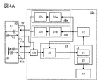
- 4A and 4B are diagrams illustrating a configuration example of the measuring device.
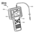
- 5A and 5B are diagrams illustrating a configuration example of the measuring device.
- 6A to 6C are diagrams illustrating a configuration example of the probe.
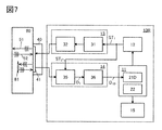
- FIG. 7 is a diagram illustrating a configuration example of the measuring device.
- 8A and 8B are diagrams illustrating a configuration example of a storage device.
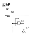
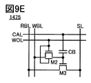
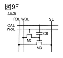
- 9A to 9H are diagrams illustrating a configuration example of a storage device.
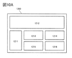
- 10A and 10B are diagrams illustrating a configuration example of a storage device.
- FIG. 11 is a diagram illustrating a configuration example of a semiconductor device.
- FIG. 12 is a diagram illustrating a configuration example of a semiconductor device.
- One aspect of the present invention is a measuring apparatus that can be used as a nondestructive inspection apparatus using ultrasonic waves such as an ultrasonic flaw detection apparatus.
- a thickness measurement device, a hardness measurement device, a sound velocity measurement device, or the like using ultrasonic waves can be realized.
- FIG. 1 is a block diagram showing a configuration of a measuring device 10 according to one embodiment of the present invention. Further, in FIG. 1, a probe 40 connected to the measuring device 10 and a sample 80 as a measurement target are clearly shown.
- the measuring device 10 includes a control unit 11, a timing circuit unit 12, a transmission unit 13, a reception unit 14, and a display unit 15.
- the measuring device 10 has the display unit 15 as the output means here, the display unit 15 does not necessarily have to be provided.
- the measuring device 10 may have an output unit such as an external output terminal or a wireless communication unit for outputting measurement data, an image signal described later, or the like to an external device, instead of the display unit 15.
- the measuring device 10 may have both the display unit 15 and the output unit.
- the probe 40 that can be connected to the measuring device 10 has a piezoelectric element 41.
- the probe 40 can generate an ultrasonic wave 51 by the piezoelectric element 41 based on the pulse signal input from the measuring device 10. Further, the piezoelectric element 41 can receive the reflected wave 52 from the specimen 80 and convert it into an electric signal.
- the probe 40 can output the electric signal to the measuring device 10 as an input signal of the measuring device 10.
- ultrasonic waves are generated while the probe 40 is in contact with the sample 80, and the ultrasonic wave 51 propagates inside the sample 80, and a reflected wave 52 from the sample 80 to the probe 40.
- the state of input is schematically shown.
- the ultrasonic wave 51 is reflected by the surface of the specimen 80 opposite to the contact surface of the probe 40.
- the ultrasonic wave 51 is reflected by the scratch 81.
- the period from the time when the ultrasonic wave 51 is generated until the reflected wave 52 reaches the piezoelectric element 41 differs depending on the presence or absence of the scratch 81, not only the presence or absence of the scratch 81 but also the position or depth of the scratch 81 You can find out. Further, by analyzing the difference in amplitude of the reflected wave 52 when the probe 40 is moved along the surface of the sample 80, the shape and size of the scratch 81 can be estimated.
- the control unit 11 has a function of comprehensively controlling each component of the measuring device 10.
- the control unit 11 includes at least a storage unit 21 and a calculation unit 22.
- the timing circuit unit 12 has a function of outputting a timing signal ST 1 and a timing signal ST 2 to the transmission unit 13 and the reception unit 14, respectively, in response to a command from the control unit 11.
- the transmitter 13 has a function of generating and outputting a pulse signal to be output to the probe 40.
- the transmission unit 13 has a configuration including a pulse signal generation unit 31 and an amplification unit 32.
- the pulse signal generator 31 generates a pulse signal according to the timing signal ST 1 and outputs it to the amplifier 32.
- the amplification unit 32 has a function of amplifying the amplitude of the pulse signal generated by the pulse signal generation unit 31 and outputting it to the probe 40.
- the receiving unit 14 has a function of sampling the analog signal input from the probe 40 to generate analog data, and a potential suitable for inputting the potential of the sampled analog data to the storage unit 21 of the control unit 11. adjust (also referred to as amplification) to have a function of generating an analog data D 1, and a function of outputting the analog data D 1 to the control unit 11 generated, and.
- the receiving unit 14 has a configuration including an amplifying unit 35.
- the amplification unit 35 samples the analog signal input from the probe 40 according to the timing signal ST 2 , and further amplifies the potential of the analog data obtained by sampling to generate the analog data D 1 . Output to the control unit 11.
- the user can set the amplitude, frequency, duty ratio, pulse shape, and the like of the pulse signal output by the transmission unit 13.
- the control unit 11 can output a desired pulse signal by controlling the timing circuit unit 12 based on information preset by the user.
- the sampling timing of the receiving unit 14 is also preferably settable by the user.
- the control unit 11 controls the timing circuit unit 12 based on the information preset by the user, so that the input analog signal can be sampled at a desired timing.
- the storage unit 21 included in the control unit 11 has a function of storing analog data as an analog value.
- the control unit 11 can store the analog data D 1 input from the receiving unit 14 in the storage unit 21 as it is, without converting the analog data D 1 into digital data.
- analog data refers to data that represents information in a continuous amount (for example, data potential).
- digital data refers to data that represents information in discrete quantities. Therefore, not only the data expressed in binary, but also the multi-valued data of three or more values are included in the digital data.
- the storage unit 21 preferably has a configuration capable of storing an analog value in one memory cell.
- the amount of information per memory cell can be significantly increased as compared with a storage unit to which a memory cell that stores binary digital data of 0 or 1 is applied. Therefore, the occupied area of the memory cell array applied to the storage unit 21 can be made extremely small. Further, the writing speed and the reading speed of the data of the storage unit 21 can be significantly increased for the same amount of information, and the power consumption can be reduced.
- FIG. 7 illustrates a configuration including a storage unit 21D that stores digital data instead of the storage unit 21 in FIG.
- the receiving unit 14 needs to be provided with an analog-digital conversion unit 36 for converting the analog data D 1 generated by the amplification unit 35 into digital data D 1D . Therefore, not only the circuit scale of the receiving unit 14 is expanded, but also the power consumption of the receiving unit 14 is increased.
- the measuring device 10 shown in FIG. 1 compared with the configuration shown in FIG. 7, not only can the circuit scale of the receiving unit 14 be reduced, but also the power consumption can be reduced. Furthermore, the circuit scale and power consumption of the control unit 11 may be reduced in some cases. With such a configuration, the number of parts of the measuring device 10 can be reduced, and the measuring device 10 can be manufactured at low cost. In addition, the measuring device 10 can be made smaller and lighter, and can be easily carried. In particular, for the purpose of flaw detection inspection, since the inspection target may be a large-scale object such as a building or a tunnel, it is extremely important to reduce the size and weight of the device.
- a memory circuit also referred to as an analog memory
- a transistor including an oxide semiconductor can have extremely low leakage current (off current) in an off state as compared with a transistor including silicon, so that power consumption in standby can be suppressed.
- an analog potential input to the memory cell can be held for a long time; thus, an analog memory in which data fluctuation is less likely to occur is formed. be able to.
- the calculation unit 22 included in the control unit 11 has a function of generating the image signal S 0 based on the analog data D 1 stored in the storage unit 21.
- the control unit 11 can output the image signal S 0 generated by the calculation unit 22 to the display unit 15.
- the arithmetic unit 22 may be configured to be capable of digital arithmetic processing, but is particularly preferably configured to be capable of analog arithmetic processing. As a result, it is not necessary to convert the analog data D 1 stored in the storage unit 21 into digital data for processing, so that the circuit scale of the control unit 11 can be reduced.
- the image that can be displayed on the display unit 15 includes an image including the waveform of the received ultrasonic wave and a two-dimensional mapping image obtained by analyzing the waveform. It is preferable that the user can select the information to be displayed on the display unit 15.
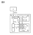
- FIG. 2 is a block diagram showing an example of the configuration of the display unit 15.
- the display unit 15 includes a pixel unit 61, a source driver circuit 62, a gate driver circuit 63, a timing circuit 64, and the like.
- the pixel portion 61 has a plurality of pixels 75 arranged in a matrix.
- a plurality of source lines SL to which a signal S 2 is input as an image signal (also referred to as a video signal) from a source driver circuit 62 and a plurality of signals to which a signal G is input as a selection signal from a gate driver circuit 63 are input.
- the timing circuit 64 outputs a signal (clock signal CLK S , clock signal CLK G and start signal) to the source driver circuit 62 or the gate driver circuit 63 based on the synchronization signal included in the image signal S 0 input from the control unit 11. Pulse signal).
- the timing circuit 64 also has a function of generating a signal S 1 to be output to the source driver circuit 62 from the image signal S 0 .
- the source driver circuit 62 has a function of generating a signal S 2 to be output to each source line SL from the signal S 1 and sequentially outputting the signal S 2 to each source line SL according to the timing signal CLK S.
- the gate driver circuit 63 in accordance with the timing signal CLK G, has a function of sequentially selecting each gate line GL, and outputs a signal G to the gate line GL selected.
- FIG. 2 shows an example in which the source driver circuit 62 has a sequential circuit 71 and a level shift circuit 72. Note that the source driver circuit 62 may have a buffer circuit or the like. Further, when the signal S 1 input from the timing circuit 64 is digital data, a configuration including a DA conversion circuit may be used.
- the sequential circuit 71 includes, for example, a shift register circuit and a latch circuit.
- the signal S 1 input to the sequential circuit 71 is sampled based on the timing signal generated by the shift register circuit and output to the level shift circuit 72.
- the level shift circuit 72 has a function of converting the potential of the signal input from the sequential circuit 71 into a potential output to the source line SL.
- the level shift circuit 72 can increase the amplitude of the voltage of the input signal and output it.
- the circuits located upstream of the level shift circuit 72 for example, the sequential circuit 71, the timing circuit 64, etc.
- the circuits located upstream of the level shift circuit 72 can be driven with a low voltage, and thus high-speed operation becomes easy.
- the image signal S 0 input from the control unit 11 includes an analog signal. That is, the image signal S 0 is preferably a signal including the analog data D 2 associated with the coordinates of each pixel of the pixel unit 61. As a result, it is not necessary to provide the D / A conversion circuit in the source driver circuit 62, so that the circuit configuration can be simplified.
- the potential of the analog data D 2 included in the image signal S 0 is preferably equal to the potential of the analog data D 1 stored in the storage unit 21.
- the drive voltage (or power supply voltage) of the timing circuit 64 or the sequential circuit 71 of the source driver circuit 62 can be made common with the drive voltage of the storage unit 21.
- the information of the two-dimensional map can be represented by the brightness of each pixel 75.
- the gradation (that is, the brightness) of the pixel 75 is determined based on the potential of the analog data D 2 included in the image signal S 0 , so that the image signal in the arithmetic unit 22 included in the control unit 11 is determined. It is possible to reduce the load of calculation processing in the generation of.
- the source driver circuit 62 is preferably configured to convert the potential of the analog data D 2 input from the sequential circuit 71 by the level shift circuit 72 and output it to the source line SL.
- FIG. 3A shows a block diagram of the measuring apparatus 10a to which the probe 40 having two piezoelectric elements (piezoelectric element 41a and piezoelectric element 41b) is connected.
- the measuring device 10a mainly includes two transmitting units (transmitting units 13a and 13b) and two receiving units (receiving units 14a and 14b) as compared with the measuring device 10 described above. It's different. It should be noted that although the configuration has two transmitting units and two receiving units here for ease of explanation, three or more transmitting units and three receiving units may be provided depending on the configuration of the probe 40.
- the transmitter 13a has a pulse signal generator 31a and an amplifier 32a.
- the transmitter 13b has a pulse signal generator 31b and an amplifier 32b.
- the transmitter 13a has a function of generating and outputting a pulse signal to be output to the piezoelectric element 41a of the probe 40.
- the transmitter 13b has a function of generating and outputting a pulse signal to be output to the piezoelectric element 41b.
- Each of the pulse signal generation unit 31a and the pulse signal generation unit 31b can generate a pulse signal according to a timing signal (not shown) individually input from the timing circuit unit 12. Therefore, not only can the amplitude, frequency, duty ratio, and pulse shape of the pulse signal output to each of the piezoelectric element 41a and the piezoelectric element 41b be set individually, but also the timing of the pulse signal output to two can be set individually. Thereby, various measuring methods can be selected, and the measuring device 10a having higher versatility can be obtained.
- the receiver 14a has an amplifier 35a.
- the reception unit 14b has an amplification unit 35b.
- the reception unit 14a receives the signal received by the piezoelectric element 41a, amplifies the signal, and outputs the amplified signal to the control unit 11.
- the receiving unit 14b receives the signal received by the piezoelectric element 41b, amplifies the signal, and outputs it as an analog signal to the control unit 11.
- the receiving unit 14a and the receiving unit 14b can individually receive signals and output them to the control unit 11. Therefore, the data of the reflected waves 52 respectively received by the two piezoelectric elements 41a and 41b at different positions can be acquired at the same time. As a result, more diverse measuring methods can be realized and the measuring device 10a with high accuracy can be obtained.
- the measuring apparatus 10b shown in FIG. 3B mainly differs from the measuring apparatus 10 in that it has two selection circuits (selection circuit 15a and selection circuit 15b).
- the selection circuits 15a and 15b each have a function of selecting and outputting a signal, and can also be referred to as a signal selection unit.
- the selection circuit 15a has a function of selecting which of the piezoelectric element 41a and the piezoelectric element 41b the pulse signal input from the transmission unit 13 is output to.
- the selection circuit 15a one transmitting unit 13 can output a pulse signal to a plurality of piezoelectric elements, so that the configuration of the measuring device can be simplified.
- the selection circuit 15b has a function of selecting which of the signals input from each of the piezoelectric element 41a and the piezoelectric element 41b to be output to the receiving unit 14. Since it is not necessary to provide a plurality of receiving units 14 by the selection circuit 15b, the configuration of the measuring device can be simplified.
- the measuring apparatus 10b shown in FIG. 3B can preferably use a measuring method in which a plurality of piezoelectric elements included in the probe 40 are sequentially operated to acquire data.
- the measuring apparatus 10c shown in FIG. 4A mainly differs from the measuring apparatus 10 in that it has two transmitting units (transmitting unit 13a and transmitting unit 13b) and a selection circuit 15b.
- the measuring device 10c has a configuration in which pulse signals are supplied to the piezoelectric element 41a and the piezoelectric element 41b from different transmitters, and the signal from one of the piezoelectric elements is output to the controller 11 as an analog signal.
- the measuring apparatus 10d shown in FIG. 4B mainly differs from the measuring apparatus 10 in that it has a selection circuit 15a and two receiving sections (receiving section 14a and receiving section 14b).
- the measuring device 10d can preferably use a measuring method in which ultrasonic waves are sequentially generated from the piezoelectric element 41a and the piezoelectric element 41b, and information of the two piezoelectric elements is acquired at the same time.
- one piezoelectric element is used for both transmission and reception has been described, but one of the two piezoelectric elements may be used for transmission and the other may be used for reception. Good. Further, a plurality of transmitting piezoelectric elements and a plurality of receiving piezoelectric elements may be arranged side by side. At this time, the number of transmitting piezoelectric elements may differ from the number of receiving piezoelectric elements, or only one of them may be provided. For example, one piezoelectric element for transmission and a plurality of piezoelectric elements for reception may be arranged.
- FIG. 5A shows an external view of the measuring device 100a.
- the measuring device 100a can be driven by, for example, a built-in battery (preferably a secondary battery such as a lithium ion battery) and can be carried. Since the measuring device 100a is small and lightweight, it is possible to easily perform ultrasonic flaw detection even in a place where it is difficult to carry a large device.
- a built-in battery preferably a secondary battery such as a lithium ion battery
- the measuring device 100a has a housing 101, a display unit 102, operation buttons 103, and the like.
- a connector cable 107 for connecting to the probe is connected to the measuring device 100a.
- a protective member 104 for protecting the casing 101 of the measuring device 100a is attached.
- a material having high impact resistance, weather resistance, and chemical resistance, such as rubber, as the protective member 104 it is possible to have a structure that can withstand use in various environments.
- the measuring device 100a has a supporting member 105.
- the support member 105 can rotate around the shaft portion, and can hold the housing 101 in a state of being inclined at a desired angle. Further, by rotating the support member 105 above the housing 101, the support member 105 can be used also as a handle, which facilitates carrying.
- FIG. 5A as an example of the image displayed on the display unit 102, an image of the ultrasonic waveform detected by the probe is shown. Three waveforms are observed here, from the left, the waveform of the ultrasonic wave output from the probe, the waveform of the reflected wave (also called echo) from the scratch inside the specimen, and the reflected wave from the back surface of the specimen. Waveforms are respectively shown, and it can be seen from this image that there are scratches inside the specimen.
- the measuring device 100b shown in FIG. 5B is an example of a handy type measuring device.
- the measuring device 100b can be grasped and operated with one hand, and does not require a space for installation, so that the width of an object that can be inspected can be widened. Further, since the measuring device 100b is extremely lightweight and can be miniaturized, the burden on the user can be reduced even in the case of a long-term inspection.
- the portion where the display unit 102 is provided is provided with the operation buttons 103 and the like, and has a shape that is horizontally longer than the portion that the user holds. This increases the area of the display unit 102, which is preferable because the amount of information that can be provided to the user can be increased and larger characters and images can be displayed.
- the display unit 102 may also have a function as a touch panel.
- FIG. 5B shows an example of measurement results using a bevel probe as an example of an image displayed on the display unit 102.
- the distribution of echo waveform intensities in the depth direction is shown.
- a measurement range and an image visualizing the position and intensity of the observed echo waveform are shown.
- the position and intensity of the observed echo waveform are shown as a two-dimensional mapping image parallel to the surface of the sample.
- a probe also called a probe or a transducer
- the vibrator has a configuration in which a dielectric having piezoelectricity is sandwiched between a pair of electrodes.
- a vertical probe or a bevel probe there is a vertical probe or a bevel probe.
- a water immersion probe can be used.
- the vertical probe is an element that emits ultrasonic waves in a direction perpendicular to the contact surface, and a flaw detection method using such a probe is also called vertical flaw detection.
- the bevel probe is an element that emits ultrasonic waves obliquely to the contact surface, and a flaw detection method using such a probe is also called bevel flaw detection.
- the water immersion probe is an element for measuring a sample submerged in a liquid such as water via the liquid, and a flaw detection method using such a probe is also called water immersion flaw detection.
- the element serves both for transmission and reception.
- the two-transducer probe including two transducers can be divided into one for transmission and the other for reception, and can be suitably used for a specimen relatively thinner than the single-transducer probe.
- a probe in which a plurality of transducers are arranged in a one-dimensional or two-dimensional array may be used.
- FIG. 6A shows a configuration example of a probe 110a that can be used as a vertical probe.
- the probe 110a includes a vibrator 111, a case 112, a contact portion 113, a terminal portion 114, a pair of wirings 115, a damper 116, and the like.
- a vibrator 111 Inside the case 112, a vibrator 111, a damper 116, etc. are provided inside the case 112. Further, a terminal portion 114 for connecting the connector cable 107 is provided on a part of the case 112. In FIG. 6A, the connector cable 107 connected to the terminal portion 114 is indicated by a broken line.
- the pair of wirings 115 are respectively connected to a pair of electrodes (not shown) of the vibrator 111.
- the pair of wirings 115 are connected to the terminal portion 114.
- the contact part 113 is a part in contact with the sample, and can transmit the ultrasonic wave generated by the transducer 111 to the sample.
- FIG. 6B shows a configuration example of the probe 110b that functions as a bevel probe.
- the probe 110b includes a transmission member 117 and a sound absorbing member 118.
- the transmission member 117 is provided in contact with the vibrator 111 and the contact portion 113.
- the surface of the transmission member 117 that contacts the vibrator 111 has a shape that is obliquely cut with respect to the surface of the contact portion 113. Thereby, ultrasonic waves can be emitted in an oblique direction with respect to the contact surface with the sample.
- a sound absorbing member 118 is provided on the surface of the transmission member 117 that does not contact the vibrator 111 and the contact portion 113.
- the sound absorbing member 118 can prevent ultrasonic waves from being scattered on the surface of the transmitting member 117 and detected as noise, and can perform more accurate measurement.
- FIG. 6C shows a configuration example of the probe 110c that functions as a dual element probe.
- the probe 110c has a transducer 111a on the transmission side, a transducer 111b on the reception side, an acoustic isolation member 119, a pair of acoustic delay members 121, and the like.
- Each of the pair of acoustic delay members 121 has a shape in which the surface in contact with the vibrator is cut obliquely with respect to the surface of the contact portion 113.
- the vibrator 111a and the vibrator 111b are arranged in an inclined state such that the surfaces in contact with the acoustic delay member 121 face each other.
- a predetermined time difference can be provided between the time when the vibrator 111a emits an ultrasonic wave and the time when the vibrator 111b receives the ultrasonic wave. As a result, highly accurate measurement can be performed.
- an acoustic isolation member 119 is provided between the pair of acoustic delay members 121.
- the acoustic isolation member 119 can prevent ultrasonic waves emitted from the transmitter 111a on the transmission side from being directly transmitted to the vibrator 111b on the reception side.
- a transistor including an oxide as a semiconductor (hereinafter also referred to as an OS transistor) and a capacitor according to one embodiment of the present invention are applied with reference to FIGS.
- a storage device (hereinafter, sometimes referred to as an OS memory device) that is installed will be described.
- An OS memory device is a storage device including at least a capacitor and an OS transistor which controls charge and discharge of the capacitor. Since the off-state current of the OS transistor is extremely small, the OS memory device has excellent retention characteristics and can function as a nonvolatile memory.
- FIG. 8A shows an example of the configuration of the OS memory device.
- the memory device 1400 includes a peripheral circuit 1411 and a memory cell array 1470.
- the peripheral circuit 1411 includes a row circuit 1420, a column circuit 1430, an output circuit 1440, and a control logic circuit 1460.
- the column circuit 1430 has, for example, a column decoder, a precharge circuit, a sense amplifier, a write circuit, and the like.
- the precharge circuit has a function of precharging the wiring.
- the sense amplifier has a function of amplifying the data signal read from the memory cell. Note that the wiring is a wiring connected to a memory cell included in the memory cell array 1470 and will be described later in detail.
- the amplified data signal is output to the outside of the storage device 1400 as the data signal RDATA via the output circuit 1440.
- the row circuit 1420 has a row decoder, a word line driver circuit, and the like, for example, and can select a row to be accessed.
- a low power supply voltage (VSS), a high power supply voltage (VDD) for the peripheral circuit 1411, and a high power supply voltage (VIL) for the memory cell array 1470 are externally supplied to the storage device 1400. Further, a control signal (CE, WE, RE), an address signal ADDR, and a data signal WDATA are externally input to the memory device 1400.
- the address signal ADDR is input to a row decoder and a column decoder, and WDATA is input to a write circuit.
- the control logic circuit 1460 processes an external input signal (CE, WE, RE) to generate a control signal for a row decoder and a column decoder.
- CE is a chip enable signal
- WE is a write enable signal
- RE is a read enable signal.
- the signal processed by the control logic circuit 1460 is not limited to this, and another control signal may be input as necessary.
- the memory cell array 1470 has a plurality of memory cells MC and a plurality of wirings arranged in a matrix. Note that the number of wirings connecting the memory cell array 1470 and the row circuit 1420 is determined by the structure of the memory cells MC, the number of memory cells MC in one column, and the like. The number of wirings connecting the memory cell array 1470 and the column circuit 1430 is determined by the configuration of the memory cell MC, the number of memory cells MC in one row, and the like.
- FIG. 8A shows an example in which the peripheral circuit 1411 and the memory cell array 1470 are formed on the same plane
- the present embodiment is not limited to this.
- a memory cell array 1470 may be provided so as to overlap a part of the peripheral circuit 1411.
- a sense amplifier may be provided so as to overlap under the memory cell array 1470.
- FIG. 9 illustrates a configuration example of a memory cell applicable to the above memory cell MC.
- [DOSRAM] 9A to 9C show examples of circuit configurations of memory cells of DRAM.
- a DRAM including a 1-OS transistor 1-capacitive element memory cell may be referred to as a DOSRAM (Dynamic Oxide Semiconductor Random Access Memory).
- the memory cell 1471 illustrated in FIG. 9A includes the transistor M1 and the capacitor CA. Note that the transistor M1 has a gate (sometimes referred to as a top gate) and a back gate.
- a first terminal of the transistor M1 is connected to a first terminal of the capacitor CA, a second terminal of the transistor M1 is connected to a wiring BIL, a gate of the transistor M1 is connected to a wiring WOL, and a back gate of the transistor M1. Are connected to the wiring BGL.
- the second terminal of the capacitor CA is connected to the wiring CAL.
- the wiring BIL functions as a bit line
- the wiring WOL functions as a word line.
- the wiring CAL functions as a wiring for applying a predetermined potential to the second terminal of the capacitor CA. It is preferable to apply a low-level potential to the wiring CAL at the time of writing and reading data.
- the wiring BGL functions as a wiring for applying a potential to the back gate of the transistor M1. By applying an arbitrary potential to the wiring BGL, the threshold voltage of the transistor M1 can be controlled.
- the memory cell MC is not limited to the memory cell 1471, and the circuit configuration can be changed.
- the memory cell MC may have a structure in which the back gate of the transistor M1 is connected to the wiring WOL instead of the wiring BGL like the memory cell 1472 illustrated in FIG. 9B.
- the memory cell MC may be a memory cell including a transistor having a single gate structure, that is, a transistor M1 having no back gate, like the memory cell 1473 illustrated in FIG. 9C.
- the leak current of the transistor M1 can be made extremely low. That is, since the written data can be held for a long time by the transistor M1, the frequency of refreshing the memory cell can be reduced. Further, the refresh operation of the memory cell can be made unnecessary. Further, since the leak current is extremely low, multi-valued data or analog data can be held in the memory cell 1471, the memory cell 1472, and the memory cell 1473.
- the sense amplifier is provided so as to overlap under the memory cell array 1470, the bit line can be shortened. As a result, the bit line capacity is reduced and the storage capacity of the memory cell can be reduced.
- [NOSRAM] 9D to 9G show circuit configuration examples of a gain cell type memory cell having two transistors and one capacitor.
- the memory cell 1474 illustrated in FIG. 9D includes a transistor M2, a transistor M3, and a capacitor CB.
- the transistor M2 has a top gate (may be simply referred to as a gate) and a back gate.
- NOSRAM Nonvolatile Oxide Semiconductor RAM
- a first terminal of the transistor M2 is connected to a first terminal of the capacitor CB, a second terminal of the transistor M2 is connected to a wiring WBL, a gate of the transistor M2 is connected to a wiring WOL, and a back gate of the transistor M2.
- the second terminal of the capacitor CB is connected to the wiring CAL.
- the first terminal of the transistor M3 is connected to the wiring RBL, the second terminal of the transistor M3 is connected to the wiring SL, and the gate of the transistor M3 is connected to the first terminal of the capacitive element CB.
- the wiring WBL functions as a write bit line
- the wiring RBL functions as a read bit line
- the wiring WOL functions as a word line.
- the wiring CAL functions as a wiring for applying a predetermined potential to the second terminal of the capacitor CB. It is preferable that a low-level potential be applied to the wiring CAL during data writing, during data retention, and during data reading.
- the wiring BGL functions as a wiring for applying a potential to the back gate of the transistor M2. By applying an arbitrary potential to the wiring BGL, the threshold voltage of the transistor M2 can be increased or decreased.
- the memory cell MC is not limited to the memory cell 1474, and the circuit configuration can be changed as appropriate.
- the memory cell MC may have a structure in which the back gate of the transistor M2 is connected to the wiring WOL instead of the wiring BGL like the memory cell 1475 illustrated in FIG. 9E.
- the memory cell MC may be a memory cell including a transistor having a single gate structure, that is, a transistor M2 having no back gate, like the memory cell 1476 illustrated in FIG. 9F.
- the memory cell MC may have a configuration in which the wiring WBL and the wiring RBL are combined into one wiring BIL like the memory cell 1477 illustrated in FIG. 9G.
- the leak current of the transistor M2 can be made extremely low. Accordingly, the written data can be held for a long time by the transistor M2, so that the frequency of refreshing the memory cell can be reduced. Further, the refresh operation of the memory cell can be made unnecessary. Further, since the leakage current is extremely low, multi-valued data or analog data can be held in the memory cell 1474. The same applies to the memory cells 1475 to 1477.
- the transistor M3 may be a transistor including silicon in a channel formation region (hereinafter, may be referred to as a Si transistor).
- the conductivity type of the Si transistor may be an n-channel type or a p-channel type.
- the Si transistor may have higher field effect mobility than the OS transistor. Therefore, a Si transistor may be used as the transistor M3 that functions as a read transistor. Further, by using a Si transistor for the transistor M3, the transistor M2 can be provided by being stacked over the transistor M3; thus, the area occupied by the memory cell can be reduced and high integration of the memory device can be achieved.
- the transistor M3 may be an OS transistor.
- OS transistors are used for the transistors M2 and M3, the memory cell array 1470 can be formed using only n-type transistors.
- FIG. 9H shows an example of a gain cell type memory cell having three transistors and one capacitive element.
- the memory cell 1478 illustrated in FIG. 9H includes the transistors M4 to M6 and the capacitor CC.
- the capacitive element CC is provided as appropriate.
- the memory cell 1478 is electrically connected to the wiring BIL, the wiring RWL, the wiring WWL, the wiring BGL, and the wiring GNDL.
- the wiring GNDL is a wiring which gives a low-level potential. Note that the memory cell 1478 may be electrically connected to the wiring RBL and the wiring WBL instead of the wiring BIL.
- the transistor M4 is an OS transistor having a back gate, and the back gate is electrically connected to the wiring BGL. Note that the back gate and the gate of the transistor M4 may be electrically connected to each other. Alternatively, the transistor M4 may not have a back gate.
- the transistors M5 and M6 may be n-channel Si transistors or p-channel Si transistors, respectively.
- the transistors M4 to M6 may be OS transistors.
- the memory cell array 1470 can be formed using only n-type transistors.
- the leak current of the transistor M4 can be made extremely low.
- peripheral circuit 1411 the memory cell array 1470, and the like shown in this embodiment are not limited to the above. Arrangement or function of these circuits and wirings, circuit elements, and the like connected to the circuits may be changed, deleted, or added as necessary.
- an example of the chip 1200 is shown with reference to FIG.
- a plurality of circuits (systems) are mounted on the chip 1200.
- the technology for integrating a plurality of circuits (systems) into one chip in this way is sometimes called system on chip (SoC).
- SoC system on chip
- the chip 1200 includes a CPU 1211, a GPU 1212, one or more analog arithmetic units 1213, one or more memory controllers 1214, one or more interfaces 1215, one or more network circuits 1216, and the like.
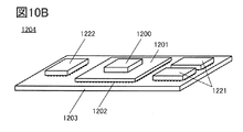
- a bump (not shown) is provided on the chip 1200 and is connected to the first surface of a printed circuit board (Printed Circuit Board: PCB) 1201 as shown in FIG. 10B. Further, a plurality of bumps 1202 are provided on the back surface of the first surface of the PCB 1201 and are connected to the mother board 1203.
- PCB printed Circuit Board
- the motherboard 1203 may be provided with a storage device such as a DRAM 1221, a flash memory 1222, or the like.
- a storage device such as a DRAM 1221, a flash memory 1222, or the like.
- the DOSRAM described in any of the above embodiments can be used as the DRAM 1221.
- the NOSRAM described in any of the above embodiments can be used for the flash memory 1222.
- the CPU 1211 preferably has a plurality of CPU cores.
- the GPU 1212 preferably has a plurality of GPU cores.
- the CPU 1211 and the GPU 1212 may each have a memory that temporarily stores data.
- a memory common to the CPU 1211 and the GPU 1212 may be provided in the chip 1200.
- the above-mentioned NOSRAM or DOSRAM can be used.
- the GPU 1212 is suitable for parallel calculation of a large number of data and can be used for image processing and product-sum calculation. By providing the GPU 1212 with an image processing circuit using the oxide semiconductor of the present invention or a product-sum operation circuit, image processing and product-sum operation can be performed with low power consumption.
- the CPU 1211 and the GPU 1212 can also suitably execute analog calculation.
- the CPU 1211 and the GPU 1212 are provided on the same chip, wiring between the CPU 1211 and the GPU 1212 can be shortened, data transfer from the CPU 1211 to the GPU 1212, data transfer between the memories of the CPU 1211 and the GPU 1212, After the calculation by the GPU 1212, the calculation result can be transferred from the GPU 1212 to the CPU 1211 at high speed.
- the analog operation unit 1213 has one or both of an A / D (analog / digital) conversion circuit and a D / A (digital / analog) conversion circuit. Further, the above-described product-sum operation circuit may be provided in the analog operation unit 1213.
- the memory controller 1214 includes a circuit functioning as a controller of the DRAM 1221 and a circuit functioning as an interface of the flash memory 1222.
- the memory controller 1214 has a function of communicating analog data with the DRAM 1221 or the flash memory 1222.
- the interface 1215 has an interface circuit with an externally connected device such as a display device, a speaker, a microphone, a camera, and a controller.
- the controller includes a mouse, a keyboard, a game controller, and the like.
- USB Universal Serial Bus
- HDMI registered trademark
- High-Definition Multimedia Interface or the like can be used.
- the network circuit 1216 has a network circuit such as a LAN (Local Area Network). Further, a circuit for network security may be included.
- LAN Local Area Network
- the above circuit (system) can be formed on the chip 1200 by the same manufacturing process. Therefore, even if the number of circuits required for the chip 1200 increases, it is not necessary to increase the manufacturing process, and the chip 1200 can be manufactured at low cost.
- the PCB 1201 provided with the chip 1200 having the GPU 1212, the DRAM 1221, and the motherboard 1203 provided with the flash memory 1222 can be referred to as a GPU module 1204.
- the GPU module 1204 Since the GPU module 1204 has the chip 1200 using the SoC technology, its size can be reduced. Further, since it is excellent in image processing, it is suitable for use in portable electronic devices such as smartphones, tablet terminals, laptop PCs, portable (carry-out) game machines, and the like.
- a product-sum operation circuit using the GPU 1212 enables deep neural networks (DNN), convolutional neural networks (CNN), recurrent neural networks (RNN), self-encoders, deep Boltzmann machines (DBM), deep belief networks (
- DNN deep neural networks
- CNN convolutional neural networks
- RNN recurrent neural networks
- DBM deep Boltzmann machines
- the chip 1200 can be used as an AI chip, or the GPU module 1204 can be used as an AI system module because a technique such as DBN) can be performed.
- the semiconductor device illustrated in FIG. 11 includes a transistor 300, a transistor 500, and a capacitor 800.
- 13A is a cross-sectional view of the transistor 500 in the channel length direction
- FIG. 13B is a cross-sectional view of the transistor 500 in the channel width direction
- FIG. 13C is a cross-sectional view of the transistor 300 in the channel width direction.
- the transistor 500 is a transistor (OS transistor) having a metal oxide in a channel formation region. Since the off-state current of the transistor 500 is small, writing data can be held for a long time by using the transistor 500 as an OS transistor included in a semiconductor device.
- OS transistor transistor having a metal oxide in a channel formation region. Since the off-state current of the transistor 500 is small, writing data can be held for a long time by using the transistor 500 as an OS transistor included in a semiconductor device.
- the semiconductor device described in this embodiment includes a transistor 300, a transistor 500, and a capacitor 800 as illustrated in FIG.
- the transistor 500 is provided above the transistor 300
- the capacitor 800 is provided above the transistor 300 and the transistor 500.
- the transistor 300 is provided over the substrate 311, and includes a conductor 316, an insulator 315, a semiconductor region 313 formed of part of the substrate 311, a low resistance region 314a which functions as a source region or a drain region, and a low resistance region 314b. .
- the transistor 300 can be applied to, for example, the transistor included in the memory in any of the above embodiments.
- the transistor 300 As shown in FIG. 13C, in the transistor 300, the upper surface of the semiconductor region 313 and the side surface in the channel width direction are covered with the conductor 316 with the insulator 315 interposed therebetween. As described above, when the transistor 300 is a Fin type, the effective channel width is increased, so that the on-state characteristics of the transistor 300 can be improved. In addition, since the electric field contribution of the gate electrode can be increased, the off characteristics of the transistor 300 can be improved.
- the transistor 300 may be either a p-channel type or an n-channel type.
- a region of the semiconductor region 313 in which a channel is formed, a region in the vicinity thereof, a low-resistance region 314a serving as a source region or a drain region, a low-resistance region 314b, or the like preferably contains a semiconductor such as a silicon-based semiconductor. It preferably includes crystalline silicon. Alternatively, it may be formed of a material having Ge (germanium), SiGe (silicon germanium), GaAs (gallium arsenide), GaAlAs (gallium aluminum arsenide), or the like. It is also possible to adopt a configuration using silicon in which the effective mass is controlled by applying stress to the crystal lattice and changing the lattice spacing. Alternatively, the transistor 300 may be a HEMT (High Electron Mobility Transistor) by using GaAs and GaAlAs.
- HEMT High Electron Mobility Transistor
- the low-resistance region 314a and the low-resistance region 314b impart an n-type conductivity imparting element such as arsenic or phosphorus, or a p-type conductivity imparting boron, in addition to the semiconductor material applied to the semiconductor region 313. Including the element to do.
- the conductor 316 functioning as a gate electrode is a semiconductor material such as silicon, a metal material, or an alloy containing an element imparting n-type conductivity such as arsenic or phosphorus, or an element imparting p-type conductivity such as boron.
- a material or a conductive material such as a metal oxide material can be used.
- the threshold voltage of the transistor can be adjusted by selecting the material of the conductor. Specifically, it is preferable to use a material such as titanium nitride or tantalum nitride for the conductor. Further, in order to achieve both conductivity and embedding properties, it is preferable to use a metal material such as tungsten or aluminum as a laminate for the conductor, and it is particularly preferable to use tungsten in terms of heat resistance.
- the transistor 300 illustrated in FIG. 11 is an example, and the structure thereof is not limited, and an appropriate transistor may be used depending on a circuit configuration or a driving method.
- the transistor 300 may have a structure similar to that of the transistor 500 including an oxide semiconductor as illustrated in FIG. Note that details of the transistor 500 will be described later.
- An insulator 320, an insulator 322, an insulator 324, and an insulator 326 are sequentially stacked so as to cover the transistor 300.
- the insulator 320, the insulator 322, the insulator 324, and the insulator 326 for example, silicon oxide, silicon oxynitride, silicon nitride oxide, silicon nitride, aluminum oxide, aluminum oxynitride, aluminum nitride oxide, aluminum nitride, or the like is used. Good.
- silicon oxynitride refers to a material having a higher oxygen content than nitrogen as its composition
- silicon oxynitride means a material having a higher nitrogen content than oxygen as its composition.
- aluminum oxynitride refers to a material having a higher oxygen content than nitrogen as its composition
- aluminum oxynitride as a material having a higher nitrogen content than oxygen as its composition. Indicates.
- the insulator 322 may have a function as a flattening film for flattening a step caused by the transistor 300 and the like provided below the insulator 322.
- the upper surface of the insulator 322 may be planarized by a planarization process using a chemical mechanical polishing (CMP) method or the like to improve planarity.
- CMP chemical mechanical polishing
- the insulator 324 it is preferable to use a film having a barrier property such that hydrogen and impurities do not diffuse from the substrate 311, the transistor 300, or the like to a region where the transistor 500 is provided.
- a film having a barrier property against hydrogen for example, silicon nitride formed by a CVD method can be used.
- silicon nitride formed by a CVD method when hydrogen is diffused into a semiconductor element including an oxide semiconductor, such as the transistor 500, characteristics of the semiconductor element might be deteriorated in some cases. Therefore, it is preferable to use a film which suppresses diffusion of hydrogen between the transistor 500 and the transistor 300.
- the film that suppresses the diffusion of hydrogen is a film in which the amount of released hydrogen is small.
- the amount of desorbed hydrogen can be analyzed using, for example, a thermal desorption gas analysis (TDS).
- TDS thermal desorption gas analysis
- the amount of desorbed hydrogen in the insulator 324 is calculated by converting the desorbed amount into hydrogen atoms per area of the insulator 324. Therefore, it may be 10 ⁇ 10 15 atoms / cm 2 or less, preferably 5 ⁇ 10 15 atoms / cm 2 or less.
- the insulator 326 preferably has a lower dielectric constant than the insulator 324.
- the dielectric constant of the insulator 326 is preferably less than 4, and more preferably less than 3.
- the relative permittivity of the insulator 326 is preferably 0.7 times or less, and more preferably 0.6 times or less that of the insulator 324.
- a conductor 328 which is connected to the capacitor 800 or the transistor 500, a conductor 330, and the like are embedded.
- the conductor 328 and the conductor 330 have a function as a plug or a wiring.
- the conductor having a function as a plug or a wiring may have a plurality of structures collectively given the same reference numeral. In this specification and the like, the wiring and the plug connected to the wiring may be integrated. That is, part of the conductor may function as a wiring, and part of the conductor may function as a plug.
- a conductive material such as a metal material, an alloy material, a metal nitride material, or a metal oxide material is used as a single layer or a laminated layer. be able to. It is preferable to use a high melting point material such as tungsten or molybdenum, which has both heat resistance and conductivity, and it is preferable to use tungsten. Alternatively, it is preferably formed of a low resistance conductive material such as aluminum or copper. Wiring resistance can be reduced by using a low-resistance conductive material.
- a wiring layer may be provided on the insulator 326 and the conductor 330.
- an insulator 350, an insulator 352, and an insulator 354 are sequentially stacked and provided.
- a conductor 356 is formed over the insulator 350, the insulator 352, and the insulator 354.
- the conductor 356 has a function of a plug connected to the transistor 300 or a wiring. Note that the conductor 356 can be provided using a material similar to that of the conductor 328 and the conductor 330.
- the insulator 350 is preferably an insulator having a barrier property against hydrogen, like the insulator 324.
- the conductor 356 preferably contains a conductor having a barrier property against hydrogen.
- a conductor having a hydrogen barrier property is formed in the opening of the insulator 350 having a hydrogen barrier property.
- tantalum nitride or the like may be used as the conductor having a barrier property against hydrogen. Further, by stacking tantalum nitride and tungsten having high conductivity, diffusion of hydrogen from the transistor 300 can be suppressed while maintaining conductivity as a wiring. In this case, it is preferable that the tantalum nitride layer having a hydrogen barrier property is in contact with the insulator 350 having a hydrogen barrier property.
- a wiring layer may be provided on the insulator 354 and the conductor 356.
- an insulator 360, an insulator 362, and an insulator 364 are sequentially stacked and provided.
- a conductor 366 is formed over the insulator 360, the insulator 362, and the insulator 364.
- the conductor 366 has a function as a plug or a wiring. Note that the conductor 366 can be provided using a material similar to that of the conductor 328 and the conductor 330.
- the insulator 360 is preferably an insulator having a barrier property against hydrogen, like the insulator 324.
- the conductor 366 preferably contains a conductor having a barrier property against hydrogen.
- a conductor having a barrier property against hydrogen is formed in the opening portion of the insulator 360 having a barrier property against hydrogen.
- a wiring layer may be provided on the insulator 364 and the conductor 366.
- an insulator 370, an insulator 372, and an insulator 374 are sequentially stacked and provided.
- a conductor 376 is formed over the insulator 370, the insulator 372, and the insulator 374.
- the conductor 376 has a function as a plug or a wiring. Note that the conductor 376 can be provided using a material similar to that of the conductor 328 and the conductor 330.
- the insulator 370 is preferably an insulator having a barrier property against hydrogen, like the insulator 324.
- the conductor 376 preferably includes a conductor having a barrier property against hydrogen.
- a conductor having a hydrogen barrier property is formed in the opening of the insulator 370 having a hydrogen barrier property.
- a wiring layer may be provided on the insulator 374 and the conductor 376.
- an insulator 380, an insulator 382, and an insulator 384 are sequentially stacked and provided.
- a conductor 386 is formed over the insulator 380, the insulator 382, and the insulator 384.
- the conductor 386 has a function as a plug or a wiring. Note that the conductor 386 can be provided using a material similar to that of the conductor 328 and the conductor 330.
- the insulator 380 it is preferable to use an insulator having a barrier property against hydrogen, like the insulator 324.
- the conductor 386 preferably contains a conductor having a barrier property against hydrogen.
- a conductor having a hydrogen barrier property is formed in the opening of the insulator 380 having a hydrogen barrier property.
- the semiconductor device has been described above, the semiconductor device according to this embodiment It is not limited to this.
- the number of wiring layers similar to the wiring layer including the conductor 356 may be three or less, or the number of wiring layers similar to the wiring layer including the conductor 356 may be five or more.
- An insulator 510, an insulator 512, an insulator 514, and an insulator 516 are sequentially stacked on the insulator 384. Any of the insulator 510, the insulator 512, the insulator 514, and the insulator 516 is preferably formed using a substance having a barrier property against oxygen and hydrogen.
- insulator 510 and the insulator 514 for example, a film having a barrier property in which hydrogen and impurities do not diffuse from the substrate 311 or a region where the transistor 300 is provided to a region where the transistor 500 is provided is used. Is preferred. Therefore, a material similar to that of the insulator 324 can be used.
- silicon nitride formed by a CVD method can be used as an example of a film having a barrier property against hydrogen.
- silicon nitride formed by a CVD method when hydrogen is diffused into a semiconductor element including an oxide semiconductor, such as the transistor 500, characteristics of the semiconductor element might be deteriorated in some cases. Therefore, it is preferable to use a film which suppresses diffusion of hydrogen between the transistor 500 and the transistor 300.
- the film that suppresses the diffusion of hydrogen is a film in which the amount of released hydrogen is small.
- a metal oxide such as aluminum oxide, hafnium oxide, or tantalum oxide is preferably used for the insulator 510 and the insulator 514.
- aluminum oxide has a high blocking effect that does not allow the film to permeate both oxygen and impurities such as hydrogen and moisture that cause fluctuations in the electrical characteristics of the transistor. Therefore, aluminum oxide can prevent impurities such as hydrogen and moisture from entering the transistor 500 during and after the manufacturing process of the transistor. In addition, release of oxygen from the oxide included in the transistor 500 can be suppressed. Therefore, it is suitable to be used as a protective film for the transistor 500.
- the same material as that of the insulator 320 can be used for the insulator 512 and the insulator 516. Further, by applying a material having a relatively low dielectric constant to these insulators, it is possible to reduce the parasitic capacitance generated between the wirings.
- a silicon oxide film, a silicon oxynitride film, or the like can be used as the insulator 512 and the insulator 516.
- a conductor 518, a conductor (eg, a conductor 503) included in the transistor 500, and the like are embedded in the insulator 510, the insulator 512, the insulator 514, and the insulator 516.
- the conductor 518 has a function of a plug connected to the capacitor 800 or the transistor 300, or a wiring.
- the conductor 518 can be provided using a material similar to that of the conductor 328 and the conductor 330.
- the conductor 510 in a region which is in contact with the insulator 510 and the insulator 514 be a conductor having a barrier property against oxygen, hydrogen, and water.
- the transistor 300 and the transistor 500 can be separated by a layer having a barrier property against oxygen, hydrogen, and water, and diffusion of hydrogen from the transistor 300 to the transistor 500 can be suppressed.
- the transistor 500 is provided above the insulator 516.
- the transistor 500 includes a conductor 503 arranged so as to be embedded in an insulator 514 and an insulator 516, and an insulator 520 arranged over the insulator 516 and the conductor 503.
- the oxide 530b arranged, the conductor 542a and the conductor 542b which are arranged apart from each other on the oxide 530b, and the conductor 542a and the conductor 542b which are arranged between the conductor 542a and the conductor 542b.
- An insulator 580 having an opening formed so as to overlap with each other, an oxide 530c provided on the bottom and side surfaces of the opening, and an insulator 550 provided on a surface where the oxide 530c is formed. Having a conductor 560 disposed on the forming surface of the insulator 550, a.
- an insulator 544 be provided between the oxide 530a, the oxide 530b, the conductor 542a, and the insulator 580 and the insulator 580.
- the conductor 560 includes a conductor 560a provided inside the insulator 550 and a conductor 560b provided so as to be embedded inside the conductor 560a. It is preferable to have.
- an insulator 574 is preferably provided over the insulator 580, the conductor 560, and the insulator 550.
- the oxide 530a, the oxide 530b, and the oxide 530c may be collectively referred to as the oxide 530.
- the transistor 500 has a structure in which three layers of an oxide 530a, an oxide 530b, and an oxide 530c are stacked in a region where a channel is formed and in the vicinity thereof, the present invention is not limited to this. Not a thing.
- a single layer of the oxide 530b, a two-layer structure of the oxide 530b and the oxide 530a, a two-layer structure of the oxide 530b and the oxide 530c, or a stacked structure of four or more layers may be provided.
- the conductor 560 is shown as a stacked structure of two layers, but the present invention is not limited to this.
- the conductor 560 may have a single-layer structure or a stacked structure including three or more layers.
- the transistor 500 illustrated in FIGS. 11 and 13A is an example, and the structure is not limited thereto, and an appropriate transistor may be used depending on a circuit configuration or a driving method.
- the conductor 560 functions as a gate electrode of the transistor, and the conductors 542a and 542b function as a source electrode or a drain electrode, respectively.
- the conductor 560 is formed so as to be embedded in the opening of the insulator 580 and the region between the conductor 542a and the conductor 542b.
- the arrangement of the conductor 560, the conductor 542a, and the conductor 542b is selected in a self-aligned manner with respect to the opening of the insulator 580. That is, in the transistor 500, the gate electrode can be arranged in a self-aligned manner between the source electrode and the drain electrode. Therefore, the conductor 560 can be formed without providing a positioning margin, so that the area occupied by the transistor 500 can be reduced. Thereby, miniaturization and high integration of the semiconductor device can be achieved.
- the conductor 560 is formed in a region between the conductor 542a and the conductor 542b in a self-aligned manner, the conductor 560 does not have a region overlapping with the conductor 542a or the conductor 542b. Accordingly, parasitic capacitance formed between the conductor 560 and the conductors 542a and 542b can be reduced. Therefore, the switching speed of the transistor 500 can be improved and high frequency characteristics can be provided.
- the conductor 560 may function as a first gate (also referred to as a top gate) electrode. Further, the conductor 503 may function as a second gate (also referred to as a bottom gate) electrode. In that case, the threshold voltage of the transistor 500 can be controlled by changing the potential applied to the conductor 503 independently of the potential applied to the conductor 560 without depending on the potential. In particular, by applying a negative potential to the conductor 503, the threshold voltage of the transistor 500 can be made higher than 0 V and off-state current can be reduced. Therefore, applying a negative potential to the conductor 503 can reduce the drain current when the potential applied to the conductor 560 is 0 V, as compared to the case where no potential is applied.
- the conductor 503 is arranged so as to overlap with the oxide 530 and the conductor 560. Thus, when a potential is applied to the conductor 560 and the conductor 503, the electric field generated from the conductor 560 and the electric field generated from the conductor 503 are connected to cover a channel formation region formed in the oxide 530.
- a structure of a transistor that electrically surrounds a channel formation region by an electric field of a first gate electrode and a second gate electrode is referred to as a surrounded channel (S-channel) structure.
- the conductor 503 has the same structure as the conductor 518, and the conductor 503a is formed in contact with the inner walls of the openings of the insulator 514 and the insulator 516, and the conductor 503b is formed further inside.
- the transistor 500 has a structure in which the conductor 503a and the conductor 503b are stacked, the present invention is not limited to this.
- the conductor 503 may be provided as a single layer or a stacked structure including three or more layers.
- the conductor 503a be made of a conductive material having a function of suppressing diffusion of impurities such as hydrogen atoms, hydrogen molecules, water molecules, and copper atoms (the above impurities are difficult to permeate).
- impurities such as hydrogen atoms, hydrogen molecules, water molecules, and copper atoms
- a conductive material having a function of suppressing diffusion of oxygen eg, at least one of oxygen atoms and oxygen molecules
- the function of suppressing the diffusion of impurities or oxygen means the function of suppressing the diffusion of any one or all of the impurities or oxygen.
- the conductor 503a since the conductor 503a has a function of suppressing diffusion of oxygen, it is possible to prevent the conductor 503b from being oxidized and decreasing in conductivity.
- the conductor 503b is preferably formed using a highly conductive conductive material containing tungsten, copper, or aluminum as its main component. In that case, the conductor 505 is not necessarily provided. Although the conductor 503b is shown as a single layer, it may have a laminated structure, for example, a laminate of titanium or titanium nitride and the above conductive material.
- the insulator 520, the insulator 522, the insulator 524, and the insulator 550 have a function as a second gate insulating film.
- the insulator 524 which is in contact with the oxide 530, it is preferable to use an insulator containing more oxygen than the oxygen which satisfies the stoichiometric composition. That is, it is preferable that the insulator 524 be formed with an excess oxygen region. By providing such an insulator containing excess oxygen in contact with the oxide 530, oxygen vacancies in the oxide 530 can be reduced and the reliability of the transistor 500 can be improved.
- an oxide material from which part of oxygen is released by heating as the insulator having an excess oxygen region.
- the oxide that desorbs oxygen by heating means that the amount of desorbed oxygen in terms of oxygen atoms is 1.0 ⁇ 10 18 atoms / cm 3 or more, preferably 1 or more in TDS (Thermal Desorption Spectroscopy) analysis.
- the surface temperature of the film during the TDS analysis is preferably 100 ° C. or higher and 700 ° C. or lower, or 100 ° C. or higher and 400 ° C. or lower.
- the insulator 522 when the insulator 524 has an excess oxygen region, the insulator 522 preferably has a function of suppressing diffusion of oxygen (eg, oxygen atoms, oxygen molecules) (the oxygen is less likely to permeate).
- oxygen eg, oxygen atoms, oxygen molecules
- the insulator 522 has a function of suppressing diffusion of oxygen and impurities, oxygen contained in the oxide 530 does not diffuse to the insulator 520 side, which is preferable. Further, the conductor 503 can be prevented from reacting with the insulator 524 and oxygen contained in the oxide 530.
- the insulator 522 is, for example, aluminum oxide, hafnium oxide, an oxide containing aluminum and hafnium (hafnium aluminate), tantalum oxide, zirconium oxide, lead zirconate titanate (PZT), strontium titanate (SrTiO 3 ), or It is preferable to use an insulator containing a so-called high-k material such as (Ba, Sr) TiO 3 (BST) in a single layer or a laminated layer. As miniaturization and higher integration of transistors progress, problems such as leakage current may occur due to thinning of the gate insulating film. By using a high-k material for the insulator functioning as a gate insulating film, it is possible to reduce the gate potential during transistor operation while maintaining the physical film thickness.
- a so-called high-k material such as (Ba, Sr) TiO 3 (BST)
- an insulator containing an oxide of one or both of aluminum and hafnium which is an insulating material having a function of suppressing diffusion of impurities and oxygen and the like (the above oxygen is difficult to permeate).
- the insulator containing one or both oxides of aluminum and hafnium it is preferable to use aluminum oxide, hafnium oxide, an oxide containing aluminum and hafnium (hafnium aluminate), or the like.
- the insulator 522 is formed using such a material, the insulator 522 suppresses release of oxygen from the oxide 530 and entry of impurities such as hydrogen from the peripheral portion of the transistor 500 into the oxide 530. Functions as a layer.
- aluminum oxide, bismuth oxide, germanium oxide, niobium oxide, silicon oxide, titanium oxide, tungsten oxide, yttrium oxide, or zirconium oxide may be added to these insulators.
- these insulators may be nitrided. Silicon oxide, silicon oxynitride, or silicon nitride may be stacked on the above insulator and used.
- the insulator 520 is preferably thermally stable.
- silicon oxide and silicon oxynitride are preferable because they are thermally stable.
- the insulator 520 and the insulator 526 which are thermally stable and have a high relative dielectric constant can be obtained.
- the insulator 520, the insulator 522, and the insulator 524 are illustrated as the second gate insulating film having a stacked-layer structure of three layers.
- the insulating film may have a single layer, two layers, or a laminated structure of four or more layers.
- the laminated structure is not limited to the same material, and may be a laminated structure made of different materials.
- a metal oxide functioning as an oxide semiconductor be used for the oxide 530 including a channel formation region.
- an In-M-Zn oxide (the element M is aluminum, gallium, yttrium, copper, vanadium, beryllium, boron, titanium, iron, nickel, germanium, zirconium, molybdenum, lanthanum, cerium, neodymium).
- the In-M-Zn oxide that can be used as the oxide 530 is preferably a CAAC-OS or a CAC-OS described later.
- an In—Ga oxide or an In—Zn oxide may be used.
- a metal oxide having a bandgap of 2 eV or more, preferably 2.5 eV or more as the metal oxide functioning as a channel formation region in the oxide 530.
- the oxide 530 has the oxide 530a below the oxide 530b, diffusion of impurities from the structure formed below the oxide 530a into the oxide 530b can be suppressed. Further, by including the oxide 530c over the oxide 530b, diffusion of impurities from the structure formed above the oxide 530c into the oxide 530b can be suppressed.
- the oxide 530 preferably has a stacked structure due to oxides in which the atomic ratio of each metal atom is different.
- the atomic ratio of the element M in the constituent elements is higher than the atomic ratio of the element M in the constituent elements in the metal oxide used for the oxide 530b. It is preferable.
- the atomic ratio of the element M to In is preferably higher than the atomic ratio of the element M to In in the metal oxide used for the oxide 530b.
- the atomic ratio of In to the element M is preferably higher than the atomic ratio of In to the element M in the metal oxide used for the oxide 530a.
- a metal oxide that can be used for the oxide 530a or the oxide 530b can be used.
- the energy at the bottom of the conduction band of the oxide 530a and the oxide 530c be higher than the energy at the bottom of the conduction band of the oxide 530b.
- the electron affinity of the oxide 530a and the oxide 530c be smaller than the electron affinity of the oxide 530b.
- the energy level at the bottom of the conduction band changes gently at the junction of the oxide 530a, the oxide 530b, and the oxide 530c.
- the energy level at the bottom of the conduction band at the junction of the oxide 530a, the oxide 530b, and the oxide 530c is continuously changed or continuously joined.
- the oxide 530a and the oxide 530b, and the oxide 530b and the oxide 530c have a common element other than oxygen (as a main component), so that a mixed layer with low density of defect states is formed.
- the oxide 530b is an In—Ga—Zn oxide
- an In—Ga—Zn oxide, a Ga—Zn oxide, gallium oxide, or the like may be used as the oxide 530a and the oxide 530c.
- the main carrier path is the oxide 530b.
- the oxide 530a and the oxide 530c have the above structure, the density of defect states in the interface between the oxide 530a and the oxide 530b and the interface between the oxide 530b and the oxide 530c can be reduced. Therefore, the influence of interface scattering on carrier conduction is reduced, and the transistor 500 can obtain high on-state current.
- the conductor 542a and the conductor 542b which function as a source electrode and a drain electrode are provided over the oxide 530b.
- Examples of the conductor 542a and the conductor 542b include aluminum, chromium, copper, silver, gold, platinum, tantalum, nickel, titanium, molybdenum, tungsten, hafnium, vanadium, niobium, manganese, magnesium, zirconium, beryllium, indium, and ruthenium. It is preferable to use a metal element selected from iridium, strontium, and lanthanum, an alloy containing the above metal element as a component, an alloy in which the above metal elements are combined, or the like.
- tantalum nitride, titanium nitride, tungsten, a nitride containing titanium and aluminum, a nitride containing tantalum and aluminum, ruthenium oxide, ruthenium nitride, an oxide containing strontium and ruthenium, an oxide containing lanthanum and nickel, and the like are used. Is preferred.
- tantalum nitride, titanium nitride, nitride containing titanium and aluminum, nitride containing tantalum and aluminum, ruthenium oxide, ruthenium nitride, oxide containing strontium and ruthenium, and oxide containing lanthanum and nickel are difficult to oxidize. It is preferable because it is a conductive material or a material that maintains conductivity even when absorbing oxygen. Further, a metal nitride film such as tantalum nitride is preferable because it has a barrier property against hydrogen or oxygen.
- the conductor 542a and the conductor 542b are shown as a single-layer structure in FIG. 13, a stacked structure of two or more layers may be used.
- a tantalum nitride film and a tungsten film may be stacked.
- a titanium film and an aluminum film may be stacked.
- a two-layer structure in which an aluminum film is stacked over a tungsten film a two-layer structure in which a copper film is stacked over a copper-magnesium-aluminum alloy film, a two-layer structure in which a copper film is stacked over a titanium film, and a tungsten film is formed over the tungsten film.
- a two-layer structure in which copper films are laminated may be used.
- a titanium film or a titanium nitride film a three-layer structure in which an aluminum film or a copper film is stacked over the titanium film or the titanium nitride film, and a titanium film or a titanium nitride film is further formed thereover, a molybdenum film, or
- a molybdenum nitride film and an aluminum film or a copper film are stacked over the molybdenum film or the molybdenum nitride film and a molybdenum film or a molybdenum nitride film is formed thereover.
- a transparent conductive material containing indium oxide, tin oxide, or zinc oxide may be used.
- regions 543a and 543b may be formed as low resistance regions at the interface of the oxide 530 with the conductor 542a (conductor 542b) and in the vicinity thereof.
- the region 543a functions as one of the source region and the drain region
- the region 543b functions as the other of the source region and the drain region.
- a channel formation region is formed in a region between the region 543a and the region 543b.
- the oxygen concentration in the region 543a (region 543b) may be reduced.
- a metal compound layer containing a metal contained in the conductor 542a (conductor 542b) and a component of the oxide 530 may be formed in the region 543a (region 543b). In such a case, the carrier concentration of the region 543a (region 543b) increases, and the region 543a (region 543b) becomes a low resistance region.
- the insulator 544 is provided so as to cover the conductors 542a and 542b and suppresses oxidation of the conductors 542a and 542b. At this time, the insulator 544 may be provided so as to cover a side surface of the oxide 530 and be in contact with the insulator 524.
- insulator 544 a metal oxide containing one kind or two or more kinds selected from hafnium, aluminum, gallium, yttrium, zirconium, tungsten, titanium, tantalum, nickel, germanium, neodymium, lanthanum, magnesium, or the like. Can be used. Alternatively, as the insulator 544, silicon nitride oxide, silicon nitride, or the like can be used.
- the insulator 544 an oxide containing one or both of aluminum and hafnium, such as aluminum oxide, hafnium oxide, aluminum, or an oxide containing hafnium (hafnium aluminate).
- hafnium aluminate has higher heat resistance than a hafnium oxide film. Therefore, crystallization is less likely to occur in heat treatment in a later step, which is preferable.
- the insulator 544 is not an essential component when the conductors 542a and 542b are materials having oxidation resistance or when the conductivity does not significantly decrease even when oxygen is absorbed. It may be appropriately designed depending on the desired transistor characteristics.
- impurities such as water and hydrogen contained in the insulator 580 can be suppressed from diffusing into the oxide 530b through the oxide 530c and the insulator 550.
- the insulator 550 functions as a first gate insulating film.
- the insulator 550 is preferably arranged in contact with the inside (top surface and side surface) of the oxide 530c.
- the insulator 550 is preferably formed using an insulator which contains excess oxygen and releases oxygen by heating.
- silicon oxide containing excess oxygen, silicon oxynitride, silicon nitride oxide, silicon nitride, silicon oxide containing fluorine, silicon oxide containing carbon, silicon oxide containing carbon and nitrogen, and vacancy are formed.
- the silicon oxide which it has can be used.
- silicon oxide and silicon oxynitride are preferable because they are stable to heat.
- oxygen is effectively supplied from the insulator 550 to the channel formation region of the oxide 530b through the oxide 530c. Can be supplied.
- the concentration of impurities such as water or hydrogen in the insulator 550 is preferably reduced.
- the thickness of the insulator 550 is preferably 1 nm or more and 20 nm or less.
- a metal oxide may be provided between the insulator 550 and the conductor 560 in order to efficiently supply the excess oxygen of the insulator 550 to the oxide 530.
- the metal oxide preferably suppresses oxygen diffusion from the insulator 550 to the conductor 560.
- diffusion of excess oxygen from the insulator 550 to the conductor 560 is suppressed. That is, a decrease in the excess oxygen amount supplied to the oxide 530 can be suppressed.
- oxidation of the conductor 560 due to excess oxygen can be suppressed.
- a material that can be used for the insulator 544 may be used.
- the insulator 550 may have a stacked-layer structure like the second gate insulating film.
- an insulator functioning as a gate insulating film is preferably formed using a high-k material and a thermal insulator.
- a layered structure of a stable material it is possible to reduce the gate potential during transistor operation while maintaining the physical film thickness. Further, it is possible to form a laminated structure that is thermally stable and has a high relative dielectric constant.
- the conductor 560 functioning as the first gate electrode is shown as a two-layer structure in FIGS. 13A and 13B, it may have a single-layer structure or a stacked structure of three or more layers.
- the conductor 560a has a function of suppressing diffusion of impurities such as hydrogen atoms, hydrogen molecules, water molecules, nitrogen atoms, nitrogen molecules, nitric oxide molecules (N 2 O, NO, NO 2, etc.), and copper atoms. It is preferable to use materials. Alternatively, a conductive material having a function of suppressing diffusion of oxygen (eg, at least one of oxygen atoms and oxygen molecules) is preferably used. Since the conductor 560a has a function of suppressing diffusion of oxygen, oxygen contained in the insulator 550 can prevent the conductor 560b from being oxidized and decreasing in conductivity.
- impurities such as hydrogen atoms, hydrogen molecules, water molecules, nitrogen atoms, nitrogen molecules, nitric oxide molecules (N 2 O, NO, NO 2, etc.), and copper atoms. It is preferable to use materials. Alternatively, a conductive material having a function of suppressing diffusion of oxygen (eg, at least one of oxygen atoms and oxygen molecules) is preferably used. Since
- the conductive material having a function of suppressing diffusion of oxygen for example, tantalum, tantalum nitride, ruthenium, ruthenium oxide, or the like is preferably used.
- an oxide semiconductor which can be applied to the oxide 530 can be used as the conductor 560a. In that case, by forming a film of the conductor 560b by a sputtering method, the electric resistance value of the conductor 560a can be reduced to be a conductor. This can be called an OC (Oxide Conductor) electrode.
- the conductor 560b is preferably made of a conductive material containing tungsten, copper, or aluminum as a main component. Since the conductor 560b also functions as a wiring, it is preferable to use a conductor having high conductivity. For example, a conductive material containing tungsten, copper, or aluminum as its main component can be used. Further, the conductor 560b may have a stacked structure, for example, a stacked structure of titanium or titanium nitride and the above conductive material.
- the insulator 580 is provided on the conductors 542a and 542b through the insulator 544.
- the insulator 580 preferably has an excess oxygen region.
- silicon oxide, silicon oxynitride, silicon nitride oxide, silicon nitride, fluorine-added silicon oxide, carbon-added silicon oxide, carbon-nitrogen-added silicon oxide, or void-containing oxide is used as the insulator 580. It is preferable to have silicon, resin, or the like.
- silicon oxide and silicon oxynitride are preferable because they are thermally stable.
- silicon oxide and silicon oxide having vacancies are preferable because an excess oxygen region can be easily formed in a later step.
- the insulator 580 preferably has an excess oxygen region. By providing the insulator 580 from which oxygen is released by heating in contact with the oxide 530c, oxygen in the insulator 580 can be efficiently supplied to the oxide 530 through the oxide 530c. Note that the concentration of impurities such as water or hydrogen in the insulator 580 is preferably reduced.
- the opening of the insulator 580 is formed so as to overlap with a region between the conductor 542a and the conductor 542b.
- the conductor 560 is formed so as to be embedded in the opening of the insulator 580 and the region between the conductors 542a and 542b.
- the conductor 560 When miniaturizing semiconductor devices, it is necessary to shorten the gate length, but it is necessary to prevent the conductivity of the conductor 560 from decreasing. Therefore, when the thickness of the conductor 560 is increased, the conductor 560 can have a shape with a high aspect ratio. In this embodiment mode, the conductor 560 is provided so as to be embedded in the opening of the insulator 580; therefore, even if the conductor 560 has a high aspect ratio, the conductor 560 can be formed without being destroyed during the process. You can
- the insulator 574 is preferably provided in contact with the top surface of the insulator 580, the top surface of the conductor 560, and the top surface of the insulator 550.
- an excess oxygen region can be provided in the insulator 550 and the insulator 580. Accordingly, oxygen can be supplied into the oxide 530 from the excess oxygen region.
- insulator 574 a metal oxide containing one kind or two or more kinds selected from hafnium, aluminum, gallium, yttrium, zirconium, tungsten, titanium, tantalum, nickel, germanium, magnesium, or the like is used. You can
- aluminum oxide has a high barrier property and can suppress the diffusion of hydrogen and nitrogen even if it is a thin film of 0.5 nm or more and 3.0 nm or less. Therefore, aluminum oxide formed by a sputtering method can have a function as a barrier film against impurities such as hydrogen as well as an oxygen supply source.
- the insulator 581 functioning as an interlayer film over the insulator 574.
- the insulator 581 preferably has a reduced concentration of impurities such as water or hydrogen in the film.
- the conductors 540a and 540b are arranged in the openings formed in the insulator 581, the insulator 574, the insulator 580, and the insulator 544.
- the conductor 540a and the conductor 540b are provided to face each other with the conductor 560 interposed therebetween.
- the conductors 540a and 540b have the same structures as conductors 546 and 548 described later.
- An insulator 582 is provided on the insulator 581.
- the insulator 582 it is preferable to use a substance having a barrier property against oxygen and hydrogen. Therefore, a material similar to that of the insulator 514 can be used for the insulator 582.
- the insulator 582 is preferably formed using a metal oxide such as aluminum oxide, hafnium oxide, or tantalum oxide.
- aluminum oxide has a high blocking effect that does not allow the film to permeate both oxygen and impurities such as hydrogen and moisture that cause fluctuations in the electrical characteristics of the transistor. Therefore, aluminum oxide can prevent impurities such as hydrogen and moisture from entering the transistor 500 during and after the manufacturing process of the transistor. In addition, release of oxygen from the oxide included in the transistor 500 can be suppressed. Therefore, it is suitable to be used as a protective film for the transistor 500.
- an insulator 586 is provided on the insulator 582.
- a material similar to that of the insulator 320 can be used.
- a material having a relatively low dielectric constant to these insulators, it is possible to reduce the parasitic capacitance generated between the wirings.
- a silicon oxide film, a silicon oxynitride film, or the like can be used as the insulator 586.
- the insulator 520, the insulator 522, the insulator 524, the insulator 544, the insulator 580, the insulator 574, the insulator 581, the insulator 582, and the insulator 586 include the conductor 546, the conductor 548, and the like. Is embedded.
- the conductor 546 and the conductor 548 have a function as a plug connected to the capacitor 800, the transistor 500, or the transistor 300, or a wiring.
- the conductor 546 and the conductor 548 can be provided using a material similar to that of the conductor 328 and the conductor 330.
- the capacitor 800 is provided above the transistor 500.
- the capacitor 800 includes a conductor 810, a conductor 820, and an insulator 830.
- the conductor 812 may be provided over the conductor 546 and the conductor 548.
- the conductor 812 has a function as a plug connected to the transistor 500 or a wiring.
- the conductor 810 has a function as an electrode of the capacitor 800. Note that the conductor 812 and the conductor 810 can be formed at the same time.
- a metal film containing an element selected from molybdenum, titanium, tantalum, tungsten, aluminum, copper, chromium, neodymium, and scandium, or a metal nitride film containing the above element as a component (Tantalum nitride film, titanium nitride film, molybdenum nitride film, tungsten nitride film) or the like can be used.
- indium tin oxide, indium oxide containing tungsten oxide, indium zinc oxide containing tungsten oxide, indium oxide containing titanium oxide, indium tin oxide containing titanium oxide, indium zinc oxide, or silicon oxide is added. It is also possible to apply a conductive material such as indium tin oxide.
- the conductor 812 and the conductor 810 have a single-layer structure in FIG. 11, the structure is not limited thereto and a stacked structure of two or more layers may be used.
- a conductor having a barrier property and a conductor having high adhesion to the conductor having high conductivity may be formed between the conductor having barrier property and the conductor having high conductivity.
- a conductor 820 is provided so as to overlap with the conductor 810 through the insulator 830.
- the conductor 820 can be formed using a conductive material such as a metal material, an alloy material, or a metal oxide material. It is preferable to use a high melting point material such as tungsten or molybdenum, which has both heat resistance and conductivity, and it is particularly preferable to use tungsten.
- a low resistance metal material such as Cu (copper) or Al (aluminum) may be used.
- An insulator 840 is provided on the conductor 820 and the insulator 830.
- the insulator 840 can be provided using a material similar to that of the insulator 320. Further, the insulator 840 may function as a flattening film that covers the uneven shape below the insulator 840.
- Metal oxide Hereinafter, metal oxides that can be used for the semiconductor layer (oxide 530) in which the channel of the transistor is formed will be described.
- a metal oxide containing nitrogen may be collectively referred to as a metal oxide. Further, a metal oxide containing nitrogen may be referred to as metal oxynitride. For example, a metal oxide containing nitrogen such as zinc oxynitride (ZnON) may be used for the semiconductor layer.
- ZnON zinc oxynitride
- CAAC c-axis aligned crystal
- CAC Cloud-Aligned composite
- CAC Cloud-Aligned Composite
- OS can be used for the semiconductor layer.
- CAC-OS or CAC-metal oxide has a conductive function in a part of the material and an insulating function in a part of the material, and the whole material has a function as a semiconductor.
- a conductive function is a function of flowing electrons (or holes) serving as carriers
- an insulating function is a function of electrons serving as carriers. It is a function that does not flow.
- a function of switching (a function of turning on / off) can be imparted to the CAC-OS or the CAC-metal oxide by causing the conductive function and the insulating function to act in a complementary manner.
- the CAC-OS or CAC-metal oxide has a conductive region and an insulating region.
- the conductive region has the above-mentioned conductive function
- the insulating region has the above-mentioned insulating function.
- a conductive region and an insulating region are separated at a nanoparticle level in a material.
- the conductive region and the insulating region may be unevenly distributed in the material.
- the conductive region is observed with its periphery blurred and connected in a cloud shape.
- the conductive region and the insulating region are dispersed in the material in a size of 0.5 nm to 10 nm, preferably 0.5 nm to 3 nm. There is.
- CAC-OS or CAC-metal oxide is composed of components having different band gaps.
- the CAC-OS or the CAC-metal oxide is composed of a component having a wide gap due to the insulating region and a component having a narrow gap due to the conductive region.
- the carrier when the carrier flows, the carrier mainly flows in the component having the narrow gap.
- the component having the narrow gap acts complementarily to the component having the wide gap, and the carrier flows to the component having the wide gap in conjunction with the component having the narrow gap. Therefore, when the CAC-OS or CAC-metal oxide is used in the channel formation region of a transistor, a high current driving force, that is, a large on-current and a high field-effect mobility can be obtained in the on state of the transistor.
- CAC-OS or CAC-metal oxide can also be referred to as a matrix composite material or a metal matrix composite material.
- the oxide semiconductor (metal oxide) is classified into a single crystal oxide semiconductor and other non-single crystal oxide semiconductors.
- the non-single-crystal oxide semiconductor include a CAAC-OS (c-axis aligned crystal line oxide semiconductor), a polycrystalline oxide semiconductor, an nc-OS (nanocrystal oxide semiconductor), and a pseudo-amorphous oxide semiconductor (a-like).
- OS amorphous-like oxide semiconductor
- amorphous oxide semiconductor amorphous oxide semiconductor.
- CAAC-OS has a crystal structure having a c-axis orientation and a plurality of nanocrystals connected in the ab plane direction and having a strain.
- the strain refers to a portion in which the orientation of the lattice arrangement is changed between a region where the lattice arrangement is uniform and another region where the lattice arrangement is uniform in the region where a plurality of nanocrystals are connected.
- Nanocrystals are basically hexagonal, but are not limited to regular hexagons, and may be non-regular hexagons.
- the strain may have a lattice arrangement such as a pentagon and a heptagon.
- a lattice arrangement such as a pentagon and a heptagon.
- the CAAC-OS is a layered crystal in which a layer containing indium and oxygen (hereinafter, an In layer) and a layer containing elements M, zinc, and oxygen (hereinafter, a (M, Zn) layer) are stacked. It tends to have a structure (also called a layered structure).
- indium and the element M can be replaced with each other, and when the element M of the (M, Zn) layer is replaced with indium, it can be expressed as an (In, M, Zn) layer.
- the indium in the In layer is replaced with the element M, it can be expressed as an (In, M) layer.
- CAAC-OS is a metal oxide with high crystallinity.
- CAAC-OS since it is difficult to confirm a clear crystal grain boundary, it can be said that a decrease in electron mobility due to the crystal grain boundary is unlikely to occur.
- CAAC-OS impurities and defects oxygen deficiency (V O:. Oxygen vacancy also referred) etc.) with less metal It can be said to be an oxide. Therefore, a metal oxide having a CAAC-OS has stable physical properties. Therefore, the metal oxide including the CAAC-OS is resistant to heat and has high reliability.
- Nc-OS has a periodic atomic arrangement in a minute region (for example, a region of 1 nm or more and 10 nm or less, particularly a region of 1 nm or more and 3 nm or less). Moreover, in the nc-OS, no regularity is found in the crystal orientation between different nanocrystals. Therefore, no orientation is observed in the entire film. Therefore, the nc-OS may not be distinguished from an a-like @ OS or an amorphous oxide semiconductor depending on an analysis method.
- indium-gallium-zinc oxide which is a kind of metal oxide including indium, gallium, and zinc
- IGZO indium-gallium-zinc oxide
- a smaller crystal for example, the above-described nanocrystal
- a large crystal here, a crystal of several mm or a crystal of several cm.
- it may be structurally stable.
- ⁇ A-like ⁇ OS is a metal oxide having a structure between an nc-OS and an amorphous oxide semiconductor.
- a-like @ OS has voids or low density regions. That is, the crystallinity of the a-like OS is lower than that of the nc-OS and the CAAC-OS.
- Oxide semiconductors have various structures, and each has different characteristics.
- the oxide semiconductor of one embodiment of the present invention may include two or more of an amorphous oxide semiconductor, a polycrystalline oxide semiconductor, an a-like @ OS, an nc-OS, and a CAAC-OS.
- the metal oxide film functioning as a semiconductor layer can be formed by using one or both of an inert gas and an oxygen gas.
- an inert gas oxygen gas
- oxygen gas oxygen gas
- the flow rate ratio of oxygen (oxygen partial pressure) at the time of forming the metal oxide film is preferably 0% to 30%, preferably 5% to 30%. Is more preferable, and 7% or more and 15% or less is further preferable.
- the oxygen flow rate ratio is high, and for example, the oxygen flow rate ratio (oxygen partial pressure) is preferably 30% or more and 100% or less. , 50% or more and 100% or less, more preferably 60% or more and 100% or less.
- the energy gap of the metal oxide is preferably 2 eV or more, more preferably 2.5 eV or more, and further preferably 3 eV or more.
- the substrate temperature at the time of forming the metal oxide film is preferably 350 ° C. or lower, more preferably room temperature or higher and 200 ° C. or lower, and further preferably room temperature or higher and 130 ° C. or lower.
- productivity can be improved, which is preferable.
- the higher the temperature during film formation the higher the crystallinity.
- the metal oxide film can be formed by a sputtering method. Besides, for example, a PLD method, a PECVD method, a thermal CVD method, an ALD method, a vacuum evaporation method, or the like may be used.
- a metal oxide having a low carrier concentration In the case of reducing the carrier concentration of the metal oxide, the concentration of impurities in the metal oxide may be lowered and the density of defect states may be lowered. In this specification and the like, low impurity concentration and low defect level density are referred to as high-purity intrinsic or substantially high-purity intrinsic.
- the impurities in the metal oxide include, for example, hydrogen, nitrogen, alkali metals, alkaline earth metals, iron, nickel, silicon and the like.
- hydrogen contained in the metal oxide reacts with oxygen bonded to the metal atom to become water, which may form oxygen deficiency in the metal oxide. If the channel formation region in the metal oxide contains oxygen vacancies, the transistor might have normally-on characteristics. Further, a defect in which hydrogen is contained in an oxygen vacancy functions as a donor, and an electron serving as a carrier may be generated. In addition, part of hydrogen may be bonded to oxygen which is bonded to a metal atom to generate an electron which is a carrier. Therefore, a transistor including a metal oxide containing a large amount of hydrogen is likely to have normally-on characteristics.
- the metal oxide may be evaluated by the carrier concentration instead of the donor concentration. Therefore, in this specification and the like, the carrier concentration which is assumed to be a state where no electric field is applied may be used as the parameter of the metal oxide, instead of the donor concentration. That is, the “carrier concentration” described in this specification and the like can be called the “donor concentration” in some cases.
- the hydrogen concentration obtained by secondary ion mass spectrometry is less than 1 ⁇ 10 20 atoms / cm 3 , preferably 1 ⁇ 10 19 atoms / cm 3. It is less than 3 , more preferably less than 5 ⁇ 10 18 atoms / cm 3 , further preferably less than 1 ⁇ 10 18 atoms / cm 3 .
- a metal oxide in which impurities such as hydrogen are sufficiently reduced is used for a channel formation region of a transistor, stable electric characteristics can be provided.
- the carrier concentration of the metal oxide in the channel formation region is preferably 1 ⁇ 10 18 cm ⁇ 3 or less, more preferably less than 1 ⁇ 10 17 cm ⁇ 3 , and more preferably 1 ⁇ 10 16 cm ⁇ 3. It is more preferably less than 1 ⁇ 10 13 cm ⁇ 3 , further preferably less than 1 ⁇ 10 12 cm ⁇ 3 .
- the lower limit of the carrier concentration in the channel formation region of the metal oxide is not particularly limited, but can be set to 1 ⁇ 10 ⁇ 9 cm ⁇ 3 , for example.
- 10, 10a to d measuring device, 11: control unit, 12: timing circuit unit, 13, 13a, 13b: transmitting unit, 14, 14a, 14b: receiving unit, 15: display unit, 15a, 15b: selecting circuit, 21: storage unit, 21D: storage unit, 22: calculation unit, 31, 31a, 31b: pulse signal generation unit, 32, 32a, 32b, 35, 35a, 35b: amplification unit, 36: analog-digital conversion unit, 40: Probe, 41, 41a, 41b: piezoelectric element, 51: ultrasonic wave, 52: reflected wave, 61: pixel portion, 62: source driver circuit, 63: gate driver circuit, 64: timing circuit, 71: sequential circuit, 72: level shift circuit, 75: pixels, 80: sample, 81: scratch, 100a, 100b: measuring device, 101: housing, 102: display section, 103: operation button, 104: protective member, 1 05: Support member, 107: Connector cable, 110a, 110b, 110c: Probe, 111,
Landscapes
- Physics & Mathematics (AREA)
- General Physics & Mathematics (AREA)
- General Health & Medical Sciences (AREA)
- Pathology (AREA)
- Life Sciences & Earth Sciences (AREA)
- Chemical & Material Sciences (AREA)
- Analytical Chemistry (AREA)
- Biochemistry (AREA)
- Health & Medical Sciences (AREA)
- Immunology (AREA)
- Acoustics & Sound (AREA)
- Signal Processing (AREA)
- Engineering & Computer Science (AREA)
- Algebra (AREA)
- Mathematical Analysis (AREA)
- Mathematical Optimization (AREA)
- Mathematical Physics (AREA)
- Pure & Applied Mathematics (AREA)
- Investigating Or Analyzing Materials By The Use Of Ultrasonic Waves (AREA)
Priority Applications (4)
| Application Number | Priority Date | Filing Date | Title |
|---|---|---|---|
| KR1020217010339A KR102959194B1 (ko) | 2018-10-11 | 2019-10-01 | 측정 장치 |
| US17/280,327 US12066409B2 (en) | 2018-10-11 | 2019-10-01 | Testing device |
| CN201980066607.0A CN112840208B (zh) | 2018-10-11 | 2019-10-01 | 测定装置 |
| JP2020550952A JP7314163B2 (ja) | 2018-10-11 | 2019-10-01 | 測定装置 |
Applications Claiming Priority (2)
| Application Number | Priority Date | Filing Date | Title |
|---|---|---|---|
| JP2018-192526 | 2018-10-11 | ||
| JP2018192526 | 2018-10-11 |
Publications (1)
| Publication Number | Publication Date |
|---|---|
| WO2020075001A1 true WO2020075001A1 (ja) | 2020-04-16 |
Family
ID=70163831
Family Applications (1)
| Application Number | Title | Priority Date | Filing Date |
|---|---|---|---|
| PCT/IB2019/058320 Ceased WO2020075001A1 (ja) | 2018-10-11 | 2019-10-01 | 測定装置 |
Country Status (4)
| Country | Link |
|---|---|
| US (1) | US12066409B2 (https=) |
| JP (1) | JP7314163B2 (https=) |
| CN (1) | CN112840208B (https=) |
| WO (1) | WO2020075001A1 (https=) |
Citations (4)
| Publication number | Priority date | Publication date | Assignee | Title |
|---|---|---|---|---|
| JPS53120874A (en) * | 1977-03-28 | 1978-10-21 | Tokyo Shibaura Electric Co | Ultrasonic diagnosing device |
| JPH04301559A (ja) * | 1991-03-29 | 1992-10-26 | Fujitsu Ltd | 超音波影像装置 |
| JP2014079569A (ja) * | 2012-09-27 | 2014-05-08 | Fujifilm Corp | 超音波診断装置、超音波画像生成方法およびプログラム |
| JP2018152399A (ja) * | 2017-03-10 | 2018-09-27 | 株式会社半導体エネルギー研究所 | 半導体装置、および半導体装置の作製方法 |
Family Cites Families (10)
| Publication number | Priority date | Publication date | Assignee | Title |
|---|---|---|---|---|
| US6128092A (en) * | 1999-07-13 | 2000-10-03 | National Research Council Of Canada | Method and system for high resolution ultrasonic imaging of small defects or anomalies. |
| EP1905073A4 (en) | 2005-06-24 | 2011-05-11 | Semiconductor Energy Lab | SEMICONDUCTOR DEVICE AND WIRELESS COMMUNICATION SYSTEM |
| DE102008042278A1 (de) | 2008-06-13 | 2009-12-24 | Ge Inspection Technologies Gmbh | Verfahren zur zerstörungsfreien Ultraschalluntersuchung sowie Vorrichtung zur Durchführung des Verfahrens |
| WO2011122280A1 (en) | 2010-03-31 | 2011-10-06 | Semiconductor Energy Laboratory Co., Ltd. | Semiconductor display device |
| US9638671B2 (en) * | 2012-05-25 | 2017-05-02 | Fbs, Inc. | Systems and methods for damage detection in structures using guided wave phased arrays |
| US10613206B2 (en) | 2014-02-26 | 2020-04-07 | Hitachi, Ltd. | Ultrasound probe and ultrasound imaging apparatus using the same |
| KR102267237B1 (ko) | 2014-03-07 | 2021-06-18 | 가부시키가이샤 한도오따이 에네루기 켄큐쇼 | 반도체 장치 및 전자 기기 |
| US9689844B2 (en) * | 2015-07-27 | 2017-06-27 | The Boeing Company | Ultrasonic inspection using flexible two-dimensional array applied on surface of article |
| KR20170084020A (ko) | 2015-10-23 | 2017-07-19 | 가부시키가이샤 한도오따이 에네루기 켄큐쇼 | 반도체 장치 및 전자 기기 |
| WO2018172881A1 (ja) | 2017-03-24 | 2018-09-27 | 株式会社半導体エネルギー研究所 | 半導体装置、表示システム及び電子機器 |
-
2019
- 2019-10-01 JP JP2020550952A patent/JP7314163B2/ja active Active
- 2019-10-01 WO PCT/IB2019/058320 patent/WO2020075001A1/ja not_active Ceased
- 2019-10-01 US US17/280,327 patent/US12066409B2/en active Active
- 2019-10-01 CN CN201980066607.0A patent/CN112840208B/zh active Active
Patent Citations (4)
| Publication number | Priority date | Publication date | Assignee | Title |
|---|---|---|---|---|
| JPS53120874A (en) * | 1977-03-28 | 1978-10-21 | Tokyo Shibaura Electric Co | Ultrasonic diagnosing device |
| JPH04301559A (ja) * | 1991-03-29 | 1992-10-26 | Fujitsu Ltd | 超音波影像装置 |
| JP2014079569A (ja) * | 2012-09-27 | 2014-05-08 | Fujifilm Corp | 超音波診断装置、超音波画像生成方法およびプログラム |
| JP2018152399A (ja) * | 2017-03-10 | 2018-09-27 | 株式会社半導体エネルギー研究所 | 半導体装置、および半導体装置の作製方法 |
Also Published As
| Publication number | Publication date |
|---|---|
| CN112840208A (zh) | 2021-05-25 |
| JP7314163B2 (ja) | 2023-07-25 |
| US20220034851A1 (en) | 2022-02-03 |
| JPWO2020075001A1 (ja) | 2021-10-14 |
| KR20210074292A (ko) | 2021-06-21 |
| US12066409B2 (en) | 2024-08-20 |
| CN112840208B (zh) | 2024-04-09 |
Similar Documents
| Publication | Publication Date | Title |
|---|---|---|
| JP7615370B2 (ja) | 半導体装置 | |
| US12426378B2 (en) | Semiconductor device and electronic device having stacked element layers on driver-circuit substrate | |
| WO2021053473A1 (ja) | 半導体装置、および半導体装置の作製方法 | |
| JP7639207B2 (ja) | 半導体装置 | |
| WO2019220259A1 (ja) | 記憶装置、半導体装置、および電子機器 | |
| JP7689533B2 (ja) | 半導体装置 | |
| JP7167038B2 (ja) | 半導体装置 | |
| WO2020170067A1 (ja) | 半導体装置および当該半導体装置を有する電気機器 | |
| WO2020157553A1 (ja) | 記憶装置 | |
| JP2025094087A (ja) | 記憶装置 | |
| JP2020102622A (ja) | 半導体装置、および半導体装置の作製方法 | |
| CN115867968A (zh) | 半导体装置的驱动方法 | |
| JP2020017327A (ja) | 記憶装置、半導体装置、および電子機器 | |
| WO2020084415A1 (ja) | 半導体装置、および半導体装置の作製方法 | |
| CN115152021A (zh) | 半导体装置 | |
| JP2024110947A (ja) | 記憶装置及び電子機器 | |
| CN114258586A (zh) | 存储单元及存储装置 | |
| TW202335185A (zh) | 記憶體裝置 | |
| JP7314163B2 (ja) | 測定装置 | |
| KR102959194B1 (ko) | 측정 장치 | |
| JP2022044110A (ja) | 記憶装置、cpu、及び電子機器 | |
| WO2020225641A1 (ja) | 半導体装置 | |
| WO2020109923A1 (ja) | 半導体装置、および半導体装置の作製方法 | |
| WO2024089571A1 (ja) | 半導体装置、半導体装置の作製方法、及び電子機器 | |
| WO2023156875A1 (ja) | 記憶装置 |
Legal Events
| Date | Code | Title | Description |
|---|---|---|---|
| 121 | Ep: the epo has been informed by wipo that ep was designated in this application |
Ref document number: 19870834 Country of ref document: EP Kind code of ref document: A1 |
|
| ENP | Entry into the national phase |
Ref document number: 2020550952 Country of ref document: JP Kind code of ref document: A |
|
| ENP | Entry into the national phase |
Ref document number: 20217010339 Country of ref document: KR Kind code of ref document: A |
|
| NENP | Non-entry into the national phase |
Ref country code: DE |
|
| 122 | Ep: pct application non-entry in european phase |
Ref document number: 19870834 Country of ref document: EP Kind code of ref document: A1 |