WO2020049956A1 - Transistor en couches minces organiques et procédé de fabrication de transistor en couches minces organiques - Google Patents
Transistor en couches minces organiques et procédé de fabrication de transistor en couches minces organiques Download PDFInfo
- Publication number
- WO2020049956A1 WO2020049956A1 PCT/JP2019/031628 JP2019031628W WO2020049956A1 WO 2020049956 A1 WO2020049956 A1 WO 2020049956A1 JP 2019031628 W JP2019031628 W JP 2019031628W WO 2020049956 A1 WO2020049956 A1 WO 2020049956A1
- Authority
- WO
- WIPO (PCT)
- Prior art keywords
- film
- organic
- layer
- sinh
- organic thin
- Prior art date
Links
Images


Classifications
-
- H—ELECTRICITY
- H10—SEMICONDUCTOR DEVICES; ELECTRIC SOLID-STATE DEVICES NOT OTHERWISE PROVIDED FOR
- H10K—ORGANIC ELECTRIC SOLID-STATE DEVICES
- H10K10/00—Organic devices specially adapted for rectifying, amplifying, oscillating or switching; Organic capacitors or resistors having a potential-jump barrier or a surface barrier
- H10K10/40—Organic transistors
- H10K10/46—Field-effect transistors, e.g. organic thin-film transistors [OTFT]
- H10K10/462—Insulated gate field-effect transistors [IGFETs]
- H10K10/468—Insulated gate field-effect transistors [IGFETs] characterised by the gate dielectrics
- H10K10/472—Insulated gate field-effect transistors [IGFETs] characterised by the gate dielectrics the gate dielectric comprising only inorganic materials
-
- H—ELECTRICITY
- H10—SEMICONDUCTOR DEVICES; ELECTRIC SOLID-STATE DEVICES NOT OTHERWISE PROVIDED FOR
- H10K—ORGANIC ELECTRIC SOLID-STATE DEVICES
- H10K10/00—Organic devices specially adapted for rectifying, amplifying, oscillating or switching; Organic capacitors or resistors having a potential-jump barrier or a surface barrier
- H10K10/40—Organic transistors
- H10K10/46—Field-effect transistors, e.g. organic thin-film transistors [OTFT]
- H10K10/462—Insulated gate field-effect transistors [IGFETs]
- H10K10/468—Insulated gate field-effect transistors [IGFETs] characterised by the gate dielectrics
- H10K10/474—Insulated gate field-effect transistors [IGFETs] characterised by the gate dielectrics the gate dielectric comprising a multilayered structure
-
- H—ELECTRICITY
- H10—SEMICONDUCTOR DEVICES; ELECTRIC SOLID-STATE DEVICES NOT OTHERWISE PROVIDED FOR
- H10K—ORGANIC ELECTRIC SOLID-STATE DEVICES
- H10K71/00—Manufacture or treatment specially adapted for the organic devices covered by this subclass
- H10K71/10—Deposition of organic active material
- H10K71/12—Deposition of organic active material using liquid deposition, e.g. spin coating
-
- H—ELECTRICITY
- H10—SEMICONDUCTOR DEVICES; ELECTRIC SOLID-STATE DEVICES NOT OTHERWISE PROVIDED FOR
- H10K—ORGANIC ELECTRIC SOLID-STATE DEVICES
- H10K71/00—Manufacture or treatment specially adapted for the organic devices covered by this subclass
- H10K71/10—Deposition of organic active material
- H10K71/18—Deposition of organic active material using non-liquid printing techniques, e.g. thermal transfer printing from a donor sheet
Definitions
- the present invention relates to an organic thin-film transistor and a method for manufacturing the organic thin-film transistor.
- organic semiconductors are composed of organic molecules that can be dissolved in various solvents, and can be formed by coating and printing techniques. Therefore, it can be used for various devices manufactured by roll-to-roll (hereinafter also referred to as RtoR).
- RtoR roll-to-roll
- Various organic thin film transistors using such an organic semiconductor have been proposed.
- a general configuration of an organic thin film transistor includes a gate electrode formed on a substrate, an insulating film covering the gate electrode, an organic semiconductor layer formed on the insulating film, a source electrode and a drain formed on the organic semiconductor layer. It has electrodes.
- many proposals have been made to make an organic thin film transistor flexible by using an organic semiconductor as a semiconductor.
- it is necessary for other materials constituting the organic thin film transistor to exhibit performance while having flexibility.
- an insulating film separating the organic semiconductor layer and the gate electrode becomes a problem. If a crack occurs in the insulating film, the current is short-circuited and a desired response speed cannot be obtained.
- an inorganic film such as a SiO 2 film and a SiN film is formed by vapor deposition as an insulating film.
- Patent Document 1 a gate electrode, an organic semiconductor film facing the gate electrode, a protective film covering a part of the organic semiconductor film, and a pair of electrodes electrically connected to the organic semiconductor film with a gap therebetween. And a source / drain electrode.
- Patent Document 1 describes that an inorganic insulating material such as silicon oxide (SiO x ) or silicon nitride (SiN x ) is used as a gate insulating film for insulating a gate electrode and an organic semiconductor film. .
- the insulating film is formed using an insulating organic material.
- Patent Document 1 describes that an organic insulating material such as polyvinyl phenol (PVP) or polyimide is used as an insulating film.
- PVP polyvinyl phenol
- polyimide polyimide
- An object of the present invention is to solve such a problem, and has high flexibility, an organic thin film transistor capable of suppressing a decrease in carrier mobility due to a pinhole or planarity of an insulating film, and an organic thin film transistor. It is to provide a manufacturing method.
- the present invention solves the problem by the following configuration.
- a gate electrode An insulating film formed over the gate electrode; An organic semiconductor layer formed on the insulating film, Having a source electrode formed on the organic semiconductor layer, and a drain electrode,
- the insulating film is an organic thin film transistor including an inorganic film made of SiNH.
- the organic thin-film transistor according to [1] wherein the ratio of the number of atoms of SiN to H in the inorganic film, SiN: H, is 1: 0.7 to 2.
- the organic thin film transistor according to [1] or [2], wherein the thickness of the inorganic film is 1 nm to 100 nm.
- the insulating film laminating step includes: After laminating a transfer type laminated film having a substrate and a transfer layer including an inorganic layer formed on the substrate on the gate electrode, The method for manufacturing an organic thin film transistor according to [9], wherein the insulating film is laminated on the gate electrode by peeling the substrate from the transfer layer.
- an organic thin film transistor having high flexibility and capable of suppressing a decrease in carrier mobility due to a pinhole or planarity of an insulating film, and a method of manufacturing the organic thin film transistor.
- FIG. 2 is a cross-sectional view conceptually illustrating an example of the organic thin film transistor of the present invention. It is sectional drawing which shows notionally another example of the organic thin-film transistor of this invention. It is sectional drawing which shows notionally another example of the organic thin-film transistor of this invention. It is sectional drawing which shows notionally another example of the organic thin-film transistor of this invention. It is sectional drawing which shows notionally another example of the organic thin-film transistor of this invention. It is a figure for explaining an example of a manufacturing method of an organic thin film transistor of the present invention. It is a figure for explaining an example of a manufacturing method of an organic thin film transistor of the present invention. It is a figure for explaining an example of a manufacturing method of an organic thin film transistor of the present invention.
- a numerical range represented by using “to” means a range including numerical values described before and after “to” as a lower limit and an upper limit.
- thickness means a length in a direction (hereinafter, a thickness direction) in which a support, a gate electrode, an insulating film, an organic semiconductor layer, and the like, which will be described later, are arranged (laminated).
- Organic thin film transistor The organic thin film transistor of the present invention, A gate electrode; An insulating film formed over the gate electrode; An organic semiconductor layer formed on the insulating film, Having a source electrode formed on the organic semiconductor layer, and a drain electrode,
- the insulating film is an organic thin film transistor including an inorganic film made of SiNH.
- FIG. 1 conceptually shows an example of the organic thin film transistor of the present invention.
- FIG. 1 is a cross-sectional view schematically showing a cross section in a direction perpendicular to the main surface of the organic thin film transistor of the present invention.
- the main surface is the largest surface of a sheet (film, plate).
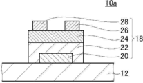
- the organic thin film transistor 10 a shown in FIG. 1 includes a support 12 and a transistor element 18 formed on the support 12.
- the transistor element 18 includes a gate electrode 20 formed on the surface of the support 12, an inorganic film (insulating film) 22 formed to cover the gate electrode 20, and an organic semiconductor layer formed on the inorganic film 22. 24, and a source electrode 26 and a drain electrode 28 formed separately on the organic semiconductor layer 24. That is, the transistor element 18 is a so-called bottom gate-top contact type transistor element.
- the support 12 side will be described as a lower side and the source electrode 26 and the drain electrode 28 side as an upper side for convenience.
- the insulating film includes an inorganic film made of SiNH (silicon hydronitride).
- the inorganic film 22 made of SiNH is an insulating film.
- the inorganic film 22 made of SiNH (hereinafter also referred to as SiNH film) is more flexible than inorganic films such as SiO (silicon oxide) film and SiN (silicon nitride) film used as an insulating film in a conventional organic thin film transistor. Excellent in nature. Further, the SiNH film is excellent in flexibility and hard to be broken, so that the insulating property due to cracks or the like is hardly reduced.
- the insulating film can have excellent insulating properties and excellent flexibility. As a result, the flexibility of the organic thin film transistor can be increased, and a decrease in carrier mobility due to pinholes and flatness of the insulating film can be suppressed.
- the ratio SiN: H of the number of atoms of SiN and H in the SiNH film 22 is preferably 1: 0.7 to 2, and more preferably 1: 0.8 to 1.8. , 1: 0.9-1.5.
- the ratio of H in the SiNH film 22 is high, the flexibility of the film is increased because the film density is reduced.
- the ratio of H is too high, the denseness of the film becomes too low, and the insulating property may be lowered.
- SiN: H by setting the ratio of the number of atoms between SiN and H, SiN: H, within the above range, both flexibility and insulation can be achieved.
- the ratio of the number of atoms between SiN and H can be measured using the RBS / HFS method (Rutherford Backscattering Spectrometry / Hydrogen Forward scattering Spectrometry). More specifically, the ratio of the number of atoms may be calculated by detecting the amounts (numbers) of the respective atoms of silicon, hydrogen, and nitrogen in the entire region in the thickness direction of the SiNH film 22 by the RBS / HFS method. . Alternatively, the number of Si, N, and H atoms on the surface of the SiNH film 22 can be measured by XPS measurement (X-ray photoelectron spectroscopy measurement), and can be calculated as the ratio between SiN and H atoms.
- the SiNH film 22 needs to have a certain thickness. From the above viewpoints, the thickness of the SiNH film 22 is preferably 1 nm to 100 nm, more preferably 5 nm to 80 nm, and still more preferably 10 nm to 50 nm.
- the structure in which the SiNH film 22 is directly laminated on the gate electrode 20 is not limited to this, and another layer is provided between the gate electrode 20 and the SiNH film 22. May be provided.
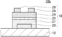
- the organic thin film transistor 10 b shown in FIG. 2 is formed on the gate electrode 20 formed on the surface of the support 12, the organic layer 21 formed so as to include the gate electrode 20, and formed on the organic layer 21. It has a SiNH film 22, an organic semiconductor layer 24 formed on the SiNH film 22, and a source electrode 26 and a drain electrode 28 formed separately on the organic semiconductor layer 24.
- the organic layer 21 is a layer serving as a base of the SiNH film 22.
- the SiNH film 22 is preferably formed by plasma CVD (Chemical Vapor Deposition). When the SiNH film 22 is formed by plasma CVD, it is difficult to form the SiNH film 22 directly on the gate electrode 20 which is a conductor.
- the SiNH film 22 can be formed by plasma CVD.
- the organic layer 21 embeds irregularities on the surface on which the SiNH film 22 is formed and foreign substances adhering to the surface.
- the surface on which the SiNH film 22 is formed is made appropriate, and the SiNH film 22 having a uniform thickness and no pinholes can be formed properly.
- the SiNH film 22 can be formed by being stacked on the gate electrode 20 by transfer.
- a transfer-type laminated film (see FIG. 7) from which the substrate can be peeled off is prepared, the substrate is peeled off from the transfer-type laminated film, and the transfer layer including the SiNH film 22 is transferred onto the gate electrode 20.
- the SiNH film 22 is formed on the organic layer 21 formed on the substrate so that the transfer layer can be peeled from the substrate.
- the organic thin film transistor having the configuration shown in FIG. 2 can be obtained by transferring the organic layer 21 toward the gate electrode 20.
- the SiNH film 22 can be formed by a desired method and conditions such as plasma CVD regardless of the configurations of the support 12 and the gate electrode 20.
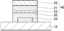
- the organic thin film transistor of the present invention includes a gate electrode 20 formed on the surface of the support 12 and an adhesive layer 30 formed so as to include the gate electrode 20, as in the organic thin film transistor 10c shown in FIG.
- the transfer type laminated film is bonded to the SiNH film 22 side via the adhesive layer 30, and then the substrate of the transfer type laminated film is separated from the transfer layer.
- the SiNH film 22 can be stacked on the gate electrode 20.
- the configuration is such that the SiNH film 22 as an insulating film is sandwiched between the adhesive layer 30 and the organic layer 21.
- the organic layer 21 is a layer serving as a base of the SiNH film 22, and it is sufficient that the organic layer 21 can be properly formed by embedding irregularities and the like on the surface on which the SiNH film 22 is formed, and does not have to have insulating properties.
- the adhesive layer 30 only needs to be able to bond the transfer layer including the SiNH film 22 onto the gate electrode 20, and does not need to have insulating properties.
- ⁇ Circle around (2) ⁇ In the case of the configuration having the organic layer 21 serving as the underlayer of the SiNH film 22, two or more combinations of the SiNH film 22 and the organic layer 21 may be provided. That is, for example, a configuration having two or more organic layers and SiNH films such as the organic layer 21, the SiNH film 22, the organic layer 21, and the SiNH film 22 on the gate electrode 20 may be adopted.
- the insulating film has a configuration including the inorganic film 22 made of SiNH.
- the present invention is not limited to this, and may have another layer.
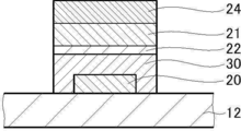
- the organic thin film transistor 10d illustrated in FIG. 4 includes an inorganic film 22 made of SiNH and a second inorganic film 23 as insulating films. Note that the organic thin film transistor 10d has the same configuration as the organic thin film transistor 10a shown in FIG. 1 except that the organic thin film transistor 10d has the second inorganic film 23.
- the second inorganic film 23 can be a known inorganic film such as a SiO (silicon oxide) film or a SiN (silicon nitride) film.
- a SiO (silicon oxide) film or a SiN (silicon nitride) film By having the second inorganic film 23, high insulating properties can be obtained. At this time, since the second inorganic film 23 is thin, the insulating property can be ensured and the flexibility is not impaired because of the presence of the SiNH film 22.
- the second inorganic film 23 it is preferable to have a SiO 2 film on the organic semiconductor layer 24 side (hereinafter also referred to as a surface layer) of the SiNH film 22.
- a SiO 2 film on the surface of the SiNH film 22 a conventionally known surface treatment performed on a surface on which an organic semiconductor such as a SAM (self-assemble monolayer) is formed can be performed. Accordingly, an organic semiconductor layer having high crystallinity is easily formed on the surface of the insulating film, and the performance of the organic thin film transistor can be improved.
- another SiNH film 22 and a second inorganic film 23 are formed so as to have a clear interface. It may be formed as a layer, or may be formed as one layer so that the ratio of SiO 2 in the surface layer of the SiNH film 22 is increased.
- the thickness of the SiO 2 film is preferably 0.1 nm to 5 nm, more preferably 0.2 nm to 3 nm, and still more preferably 0.1 nm to 1 nm.
- ⁇ Support> As the support 12, a known sheet-like material (film, plate-like material) used as a support in various organic thin film transistors can be used.
- the material of the support 12 is not limited, and various materials can be used as long as the transistor element 18 can be formed.
- the material of the support 12 include a plastic material, a silicon material, a glass material, quartz, and a ceramic material. Among them, a glass material or a plastic material is preferable from the viewpoint of applicability to each device and cost.
- the plastic material include polyester films such as polyethylene naphthalate (PEN) and polyethylene terephthalate (PET), cycloolefin polymer films, polycarbonate films, triacetyl cellulose (TAC) films, and polyimide films. Further, those obtained by bonding these plastic films to glass can also be used.
- the thickness of the substrate is not particularly limited. For example, it is preferably 10 mm or less, more preferably 2 mm or less, and particularly preferably 1.5 mm or less. On the other hand, it is preferably at least 0.01 mm, more preferably at least 0.05 mm.
- a conventionally known electrode used as a gate electrode of an organic thin film transistor can be used.
- the conductive material (also referred to as an electrode material) forming the gate electrode is not particularly limited.
- metals such as platinum, gold, silver, aluminum, chromium, nickel, copper, molybdenum, titanium, magnesium, calcium, barium, sodium, palladium, iron, and manganese; InO 2 , SnO 2 , indium tin oxide (ITO) ), Conductive metal oxides such as fluorine-doped tin oxide (FTO), aluminum-doped zinc oxide (AZO), and gallium-doped zinc oxide (GZO); polyaniline, polypyrrole, polythiophene, polyacetylene, poly (3,4-ethylenedioxy) Conductive polymers such as thiophene) / polystyrenesulfonic acid (PEDOT / PSS); acids such as hydrochloric acid, sulfuric acid and
- a film formed by a physical vapor deposition method such as a vacuum vapor deposition method, a chemical vapor deposition method (CVD method), a sputtering method, a printing method (coating method), a transfer method, a sol-gel method, or a plating method is required.
- PVD physical vapor deposition method
- CVD method chemical vapor deposition method
- sputtering method a sputtering method
- a printing method coating method
- a transfer method a sol-gel method
- a plating method There is a method of patterning a desired shape according to the method.
- a solution, a paste, or a dispersion of the above materials is prepared and applied, and a film is formed by drying, baking, photocuring, aging, or the like, or an electrode can be directly formed.
- inkjet printing can perform desired patterning, simplifying the process, reducing costs, and increasing speed. It is preferable in terms of conversion. Even when a spin coating method, a die coating method, a microgravure coating method, or a dip coating method is adopted, patterning can be performed in combination with the following photolithography method or the like.
- Examples of the photolithography method include a method of combining patterning of a photoresist with etching such as wet etching with an etchant or dry etching with reactive plasma, a lift-off method, and the like.
- etching such as wet etching with an etchant or dry etching with reactive plasma
- a lift-off method a method of irradiating the above-mentioned material with an energy beam such as a laser or an electron beam to polish or change the conductivity of the material.
- an energy beam such as a laser or an electron beam
- the thickness of the gate electrode 20 is arbitrary, but is preferably 1 nm or more, and particularly preferably 10 nm or more. Further, it is preferably at most 500 nm, particularly preferably at most 200 nm.
- the source electrode 26 is an electrode in the organic thin film transistor through which a current flows from the outside through a wiring.
- the drain electrode 28 is an electrode for sending a current to the outside through a wiring, and is usually provided in contact with the organic semiconductor layer 24.
- a conductive material used for a conventional organic thin film transistor can be used, and examples thereof include the conductive materials described for the gate electrode.
- the source electrode and the drain electrode can each be formed by a method similar to the method of forming the gate electrode.
- a lift-off method or an etching method can be employed.
- the source electrode and the drain electrode can be suitably formed by an etching method.
- the etching method is a method of removing unnecessary portions by etching after forming a conductive material.
- the conductive material remaining on the base at the time of removing the resist can be peeled off, and the resist residue and the removed conductive material can be prevented from reattaching to the base, and the shape of the electrode edge portion is excellent. In this respect, it is preferable to the lift-off method.
- a resist is applied to a part of a base, a conductive material is formed thereon, and the resist or the like is removed or removed by eluting or peeling off the resist with a solvent.
- the thickness of the source electrode 26 and the drain electrode 28 is arbitrary, but is preferably 1 nm or more, and particularly preferably 10 nm or more. Further, it is preferably at most 500 nm, particularly preferably at most 300 nm.
- the organic semiconductor layer 24 is a layer having semiconductor properties and capable of storing carriers.
- the organic semiconductor layer 24 may be a layer containing an organic semiconductor.
- the organic semiconductor is not particularly limited, and examples thereof include an organic polymer and a derivative thereof, and a low-molecular compound.
- the low molecular compound means a compound other than the organic polymer and its derivative. That is, it refers to a compound having no repeating unit.
- the molecular weight of the low molecular weight compound is not particularly limited as long as it is such a compound.
- the molecular weight of the low molecular weight compound is preferably from 300 to 2,000, more preferably from 400 to 1,000.
- Examples of the material of the organic semiconductor layer 24 include the materials described in paragraphs [0063] to [0160] of JP-A-2015-170760. Further, examples of the material of the organic semiconductor layer 24 include an organic semiconductor described in JP-A-2015-195361 and an organic semiconductor described in JP-A-2018-006745.
- the method for forming the organic semiconductor layer 24 is not particularly limited, and a conventionally known method for forming an organic semiconductor layer can be used.
- a method of forming a semiconductor active layer by dissolving a material to be an organic semiconductor layer in a solvent, applying the solution on an insulating film, and drying the solution.
- the thickness of the organic semiconductor layer 24 is arbitrary, but is preferably 0.001 ⁇ m or more, and particularly preferably 0.01 ⁇ m or more. Further, it is preferably 1 ⁇ m or less, particularly preferably 0.5 ⁇ m or less.
- SiNH film 22 is laminated between the gate electrode 20 and the organic semiconductor layer 24 and is a layer that insulates the gate electrode 20 from the organic semiconductor layer 24.
- the SiNH film 22 As described above, by using the SiNH film 22 as the insulating film, flexibility is higher than that of an inorganic film such as a SiO (silicon oxide) film or a SiN (silicon nitride) film used as an insulating film in a conventional organic thin film transistor. It is possible to obtain an excellent insulating film.
- an inorganic film such as a SiO (silicon oxide) film or a SiN (silicon nitride) film used as an insulating film in a conventional organic thin film transistor. It is possible to obtain an excellent insulating film.
- the two or more SiNH films 22 may have the same composition ratio or different composition ratios. Further, the thickness may be the same or different.
- the SiNH film 22 can be formed by a known method according to a material.
- plasma CVD such as CCP (Capacitively Coupled Plasma) -CVD and ICP (Inductively Coupled Plasm) -CVD, atomic layer deposition (ALD), sputtering such as magnetron sputtering and reactive sputtering, and vacuum
- vapor-phase film forming methods such as vapor deposition are preferably exemplified.
- plasma CVD such as CCP-CVD and ICP-CVD are preferably used.
- the second inorganic film 23 is a thin film containing an inorganic compound.
- the second inorganic film 23 has an insulating property.
- the surface properties can be made different from those of the SiNH film, and a conventionally known surface treatment performed on a surface on which an organic semiconductor is formed can be performed. it can.
- the material of the second inorganic film 23 there is no limitation on the material of the second inorganic film 23, and various types of inorganic compounds used for known organic thin film transistors, which are made of an inorganic compound exhibiting insulating properties, can be used.
- the material of the second inorganic film 23 include metal oxides such as aluminum oxide, magnesium oxide, tantalum oxide, zirconium oxide, titanium oxide, indium tin oxide (ITO); metal nitrides such as aluminum nitride; aluminum carbide Metal oxides such as silicon oxide; silicon oxides such as silicon oxide, silicon oxynitride, silicon oxycarbide, silicon oxynitride carbide; silicon nitrides such as silicon nitride and silicon nitride carbide; silicon carbides such as silicon carbide; hydrides thereof; Inorganic compounds such as mixtures of two or more of these; and hydrogen-containing substances thereof. Also, a mixture of two or more of these can be used.
- the thickness of the second inorganic film 23 is preferably 50 nm or less, more preferably 5 to 50 nm, and still more preferably 10 to 30 nm. It is preferable that the thickness of the second inorganic film 23 be 2 nm or more, since sufficient desired insulating properties and surface properties can be obtained.
- the second inorganic film 23 is generally brittle, and if it is too thick, there is a possibility that cracks, cracks, peeling, and the like may occur, and the flexibility is reduced, but the thickness of the second inorganic film 23 is reduced. By setting the thickness to 50 nm or less, it is possible to prevent the occurrence of cracks and suppress a decrease in flexibility.
- the second inorganic film 23 can be formed by a known method according to a material.
- plasma CVD such as CCP (Capacitively Coupled Plasma) -CVD and ICP (Inductively Coupled Plasm) -CVD, atomic layer deposition (ALD), sputtering such as magnetron sputtering and reactive sputtering, and vacuum
- vapor-phase film forming methods such as vapor deposition are preferably exemplified.
- plasma CVD such as CCP-CVD and ICP-CVD are preferably used.
- the organic layer 21 is a layer serving as a base layer for appropriately forming the SiNH film 22.
- the SiNH film 22 formed on the surface of the organic layer 21 is preferably formed by plasma CVD (Chemical Vapor Deposition). Therefore, when the SiNH film 22 is formed, the organic layer 21 is etched by plasma, and a mixture of the component of the organic layer 21 and the component of the SiNH film 22 is provided between the organic layer 21 and the SiNH film 22. A layer, such as a layer, is formed. As a result, the organic layer 21 and the SiNH film 22 are adhered with a very strong adhesion.
- the thickness of the organic layer 21 is a thickness of a layer that does not include the above-described mixed layer and that is formed only of the components forming the organic layer 21.
- the organic layer 21 is a base layer for properly forming the SiNH film 22
- the organic layer 21 formed on the surface of the gate electrode 20 has unevenness and surface irregularities on the surface of the gate electrode 20 and the support 12. Embed foreign substances and the like attached to As a result, the surface on which the SiNH film 22 is formed is made appropriate, and the SiNH film 22 can be formed properly.
- the organic layer 21 is a layer to which the substrate 32 is removably attached (see FIG. 7). That is, the organic layer 21 is a layer that can be separated from the substrate 32. Therefore, the adhesion between the organic layer 21 and the SiNH film 22 is stronger than the adhesion between the substrate 32 and the organic layer 21.
- the SiNH film 22 is formed by plasma CVD, the organic layer 21 is etched by plasma to form a mixed layer, and the adhesion between the organic layer 21 and the SiNH film 22 becomes extremely high. .
- the adhesion between the organic layer 21 and the SiNH film 22 is much stronger than the adhesion between the substrate 32 and the organic layer 21, and even when the substrate 32 is separated from the organic layer 21, the organic layer 21 and the SiNH film 22 are separated. 22 does not peel off.
- the transfer type laminated film from which the substrate 32 can be peeled off is realized by forming the SiNH film 22 on the organic layer 21 which makes the substrate 32 peelable.
- the organic layer 21 preferably has high heat resistance. Specifically, the organic layer 21 preferably has a glass transition temperature (Tg) of 175 ° C. or higher, more preferably 200 ° C. or higher, even more preferably 250 ° C. or higher. As described above, the SiNH film 22 formed on the surface of the organic layer 21 is preferably formed by plasma CVD. By setting the Tg of the organic layer 21 to 175 ° C. or higher, the etching and volatilization of the organic layer 21 by plasma during the formation of the SiNH film 22 are preferably suppressed, and the appropriate organic layer 21 and SiNH film 22 are preferably formed. It is preferable in that it can be formed into a non-woven fabric. The upper limit of the Tg of the organic layer 21 is not limited, but is preferably 500 ° C. or lower.
- the resin forming the organic layer 21 preferably has a large molecular weight to some extent.
- the resin forming the organic layer 21 preferably has a molecular weight (weight average molecular weight (Mw)) of 500 or more, more preferably 1000 or more, and even more preferably 1500 or more.
- the Tg of the organic layer 21 may be specified by a known method using a differential scanning calorimeter (DSC) or the like. Also, the molecular weight may be measured by a known method using gel permeation chromatography (GPC) or the like. When a commercially available product is used, the Tg and molecular weight of the organic layer 21 may be catalog values. Regarding the above points, the same applies to an adhesive layer 30 described later.
- the organic layer 21 is a layer made of, for example, an organic compound obtained by polymerizing (crosslinking, curing) a monomer, a dimer, an oligomer, and the like.
- the composition for forming the organic layer 21 may include only one type of organic compound, or may include two or more types of organic compounds.
- the organic layer 21 contains, for example, a thermoplastic resin and an organic silicon compound.
- Thermoplastic resins include, for example, polyester, (meth) acrylic resin, methacrylic acid-maleic acid copolymer, polystyrene, transparent fluororesin, polyimide, fluorinated polyimide, polyamide, polyamideimide, polyetherimide, cellulose acylate, polyurethane Polyether ether ketone, polycarbonate, alicyclic polyolefin, polyarylate, polyether sulfone, polysulfone, fluorene ring-modified polycarbonate, alicyclic modified polycarbonate, fluorene ring-modified polyester, and acrylic compound.
- the organosilicon compound include polysiloxane.
- the organic layer 21 preferably contains a polymer of a radical curable compound and / or a cationic curable compound having an ether group from the viewpoint of excellent strength and the viewpoint of a glass transition point. From the viewpoint of lowering the refractive index of the organic layer 21, the organic layer 21 preferably contains a (meth) acrylic resin whose main component is a polymer such as a (meth) acrylate monomer or oligomer. By lowering the refractive index of the organic layer 21, the transparency increases, and the light transmittance improves.
- the organic layer 21 is more preferably bifunctional or more, such as dipropylene glycol di (meth) acrylate (DPGDA), trimethylolpropane tri (meth) acrylate (TMPTA), and dipentaerythritol hexa (meth) acrylate (DPHA).
- DPGDA dipropylene glycol di (meth) acrylate
- TMPTA trimethylolpropane tri (meth) acrylate
- DPHA dipentaerythritol hexa
- acrylic resin containing as a main component a polymer such as a (meth) acrylate monomer, dimer or oligomer, and more preferably a polymer such as a trifunctional or higher-functional (meth) acrylate monomer, dimer or oligomer.
- acrylic resin containing as a main component Further, a plurality of these (meth) acrylic resins may be used.
- the main component is a component having the largest content mass ratio
- the organic layer 21 preferably contains a resin containing a bisphenol structure as a main component. More preferably, the organic layer 21 contains polyarylate (polyarylate resin (PAR)) as a main component.
- polyarylate is an aromatic polyester made of a polycondensate of a dihydric phenol such as bisphenol represented by bisphenol A and a dibasic acid such as phthalic acid (terephthalic acid, isophthalic acid). .
- the adhesion between the substrate 32 and the organic layer 21 is appropriate and easy.
- the substrate 32 can be peeled off.
- it since it has appropriate flexibility, it is possible to prevent the SiNH film 22 from being damaged (cracked or cracked) when the substrate 32 is peeled off, and it is possible to stably form an appropriate SiNH film 22 because of its high heat resistance. This is preferable in that the performance degradation of the organic thin film transistor can be prevented and the elasticity of the organic thin film transistor can be increased.
- a main component means the component with the largest content mass ratio among the components contained.
- the organic layer 21 When the organic layer 21 is formed of various resins having an aromatic ring, the organic layer 21 may be formed using a commercially available resin as long as the resin has an aromatic ring.
- Commercially available resins that can be used to form the organic layer 21 include Unifiner (registered trademark) and U Polymer (registered trademark) manufactured by Unitika Ltd., and Neoprim (registered trademark) manufactured by Mitsubishi Gas Chemical Company, Ltd. ) Are exemplified.
- the organic layer 21 can be formed by a known method according to a material.
- the organic layer 21 is prepared by preparing a composition (resin composition) in which a resin (organic compound) or the like to be the organic layer 21 is dissolved in a solvent, applying the composition to the substrate 32, and drying the composition. Can be formed.
- the resin (organic compound) in the composition may be polymerized (cross-linked) by irradiating the dried composition with ultraviolet rays as necessary.
- the composition for forming the organic layer 21 preferably contains an organic solvent, a surfactant, a silane coupling agent, and the like, in addition to the organic compound.
- the thickness of the organic layer 21 is not particularly limited. However, since the organic layer 21 serves as a base layer of the SiNH film 22, the organic layer 21 is formed by forming the SiNH film 22 to form a dense, defect-free SiNH film 22.
- the surface on which the SiNH film 22 is formed needs to be a flat surface by embedding irregularities and foreign substances on the surface of the surface.
- the SiNH film 22 is laminated on the gate electrode 20 by transfer, when the substrate 32 is peeled, it is necessary to maintain mechanical strength so that the substrate 32 is not torn at the time of peeling. Therefore, the organic layer 21 needs to have a certain thickness.
- the thickness of the organic layer 21 is preferably in the range of 0.01 ⁇ m to 1 ⁇ m, more preferably in the range of 0.03 ⁇ m to 0.8 ⁇ m, and more preferably in the range of 0.05 ⁇ m to 0.5 ⁇ m. More preferably,
- the plurality of organic layers 21 may be formed of the same material or different materials. Further, the thickness may be the same or different.
- the organic layer 21 needs to be formed so as to be peelable from the substrate 32. Therefore, a material having releasability may be used as the material of the organic layer 21 as described above, or a release layer may be provided between the organic layer 21 and the substrate 32. As the release layer, a conventionally known release layer can be appropriately used.
- the adhesive layer 30 is for bonding a transfer layer having the SiNH film 22 and the organic layer 21 onto the gate electrode 20 when the SiNH film 22 is laminated on the gate electrode 20 by transfer.
- the adhesive layer 30 is formed between the SiNH film 22 and the gate electrode 20 and the support 12 so as to embed the gate electrode 20. Further, the adhesive layer 30 also functions as a protective layer for protecting the SiNH film 22 exhibiting insulating properties.
- the adhesive layer 30 may be a conventionally known OCA (optically transparent adhesive) or an adhesive layer using a hot melt adhesive (HMA (Hot Melting Adhesive)).
- the hot melt adhesive layer is an adhesive layer that is solid at normal temperature, flows when heated, and exhibits adhesiveness.
- normal temperature is 23 degreeC.
- the adhesive layer 30 preferably flows at 30 to 200 ° C. to exhibit adhesiveness, and the adhesive layer 30 flows at 40 to 180 ° C. to exhibit adhesiveness. It is more preferable that the adhesive be flowed at 50 to 150 ° C. to exhibit adhesiveness.
- the adhesive layer 30 flows at room temperature to exhibit adhesiveness, the above-described foiling tends to occur at the time of cutting and transferring the transfer-type laminated film, resulting in a decrease in insulation performance and the like. Further, if the temperature at which the adhesive flows to develop the adhesive property is too high, the heating temperature required for attachment to the object to be attached becomes high, and the substrate 32, the organic layer 21 and the object to be attached are thermally damaged. I will.
- the Tg of the adhesive layer 30 is not limited, but is preferably 130 ° C. or lower, more preferably 100 ° C. or lower, even more preferably 60 ° C. or lower, It is particularly preferred that the temperature is 30 ° C. or lower.
- the lower limit of the Tg of the adhesive layer 30 is not limited, but is preferably ⁇ 150 ° C. or higher.
- the material of the adhesive layer 30 is not limited as long as it is solid at room temperature and can be heated to flow and exhibit adhesiveness.
- the adhesive layer 30 is preferably made of an amorphous resin as a main component, more preferably an acrylic resin as a main component, and a resin obtained by polymerizing a single acrylate monomer. (Acrylic homopolymer (homoacryl polymer)) is more preferably a main component.
- the use of an amorphous resin, particularly an acrylic resin, as the main component of the adhesive layer 30 is preferable in that a highly transparent gas barrier film can be obtained.
- the main component of the adhesive layer 30 an acrylic homopolymer, in addition to the above-mentioned advantages, transferability by heat can be improved, foil pulling can be prevented, and blocking during winding after curing is difficult. It is preferred in that respect.
- the adhesive layer 30 can be a layer that flows at a relatively low temperature to exhibit adhesiveness. Therefore, when high heat resistance is not required for the laminated film, the adhesive layer 30 made of an acrylic homopolymer is preferably used.
- the adhesive layer 30 is selected from the group consisting of a styrene acrylic copolymer (styrene-modified acrylic resin), a urethane acrylic copolymer (urethane-modified acrylic resin), and an acrylic resin for adjusting the glass transition point. May be included.
- a styrene acrylic copolymer styrene-modified acrylic resin
- a urethane acrylic copolymer urethane-modified acrylic resin
- the amounts of these components are not particularly limited, and may be appropriately determined according to the components to be added and the desired Tg. However, it is preferable that the addition amount of these components is such that the main component of the adhesive layer 30 becomes the above-mentioned amorphous resin and acrylic resin.
- the styrene acrylic copolymer, the urethane acrylic copolymer, and the acrylic resin for adjusting the glass transition point are not limited, and various resins used for adjusting Tg such as resins can be used. These components are also available as commercial products.
- the styrene acrylic copolymer is exemplified by # 7000 series manufactured by Taisei Fine Chemical Co., Ltd.
- the urethane acrylic copolymer include Acryt (registered trademark) 8UA series manufactured by Taisei Fine Chemical Co., Ltd.
- the acrylic resin for adjusting the glass transition point include PMMA (for example, Dianal (registered trademark) manufactured by Mitsubishi Chemical Corporation) and the like.
- the thickness of the adhesive layer 30 is not particularly limited, but the adhesive layer 30 needs to have a certain thickness from the viewpoint of obtaining sufficient adhesion.
- the thickness of the adhesive layer 30 is preferably small from the viewpoint of reducing the weight and thickness of the entire organic thin film transistor. From the above viewpoint, the thickness of the adhesive layer is preferably in the range of 20 ⁇ m to 0.1 ⁇ m, more preferably in the range of 5 ⁇ m to 0.3 ⁇ m, and further preferably in the range of 2 ⁇ m to 0.5 ⁇ m. preferable.
- the method for manufacturing an organic thin film transistor of the present invention includes: A gate electrode forming step of forming a gate electrode on the support, An insulating film laminating step of laminating an insulating film on the gate electrode, An organic semiconductor layer forming step of forming an organic semiconductor layer on the insulating film and a source / drain electrode forming step of forming a source electrode and a drain electrode on the organic semiconductor layer,
- the insulating film is a method for manufacturing an organic thin film transistor including an inorganic layer made of SiNH.
- the manufacturing method described below is a method for manufacturing an organic thin film transistor 10c having an adhesive layer 30 and an organic layer 21 above and below a SiNH film 22, as shown in FIG.
- a gate electrode is formed on the support 12 as shown in FIG.
- the material and forming method of the gate electrode 20 are as described above.
- an insulating film is stacked on the gate electrode 20 in an insulating film stacking step.
- an adhesive layer 30 is formed on the gate electrode 20.
- a transfer type laminated film 40 having a substrate 32 as shown in FIG. 7 and a transfer layer having the organic layer 21 and the SiNH film 22 is prepared.
- the transfer type laminated film 40 can peel the substrate 32 from the transfer layer.
- the substrate 32 a known sheet-like material (film, plate-like material) used as a substrate (support) in various laminated functional films or the like can be used. Further, as the substrate 32, various sheet materials used as separators (light release separators and heavy release separators) in various optical transparent adhesives (OCA (Optical Clear Adhesive)) can be used.
- OCA optical Clear Adhesive
- Such a transfer type laminated film 40 is produced by forming the organic layer 21 on the substrate 32 by the above-described method, and further forming the SiNH film 22 on the organic layer 21 by the above-mentioned method. Can be.
- the transfer type laminated film 40 may have a protective film on the SiNH film 22.
- the protective film may be peeled off before the transfer.
- such a transfer type laminated film 40 is laminated by bonding the SiNH film 22 side to the adhesive layer 30. Heating, pressure bonding, etc. may be performed as necessary.
- the substrate 32 is peeled off, and the SiNH film 22 as an insulating film is laminated on the gate electrode.
- an organic semiconductor layer 24 is formed on the SiNH film 22 and, in the example shown, on the organic layer 21.
- the organic semiconductor layer 24 can be formed by a conventionally known method.
- a source electrode 26 and a drain electrode 28 are formed on the organic semiconductor layer 24.
- the source electrode 26 and the drain electrode 28 can be formed by a conventionally known method. Thereby, the organic thin film transistor 10c shown in FIG. 3 is manufactured.
- the SiNH film 22 and the organic layer 21 are transferred onto the gate electrode 20 and laminated using a transfer-type laminated film having the SiNH film 22 and the organic layer 21 on the substrate 32.
- the present invention is not limited to this.
- the SiNH film 22 may be formed directly on the gate electrode 20.
- the organic layer 21 may be formed on the gate electrode 20, and the SiNH film 22 may be formed on the organic layer 21.
- each step may be performed by roll-to-roll (RtoR), or may be performed by a batch method using a cut transfer type laminated film. Further, all steps of the production of the transfer type laminated film 40 and the respective steps of the method for producing the organic thin film transistor may be performed by a series of RtoR.
- RtoR roll-to-roll
- Example 1 ⁇ Preparation of organic thin film transistor> Using a PEN (manufactured by Teijin Film Solutions Ltd.) having a thickness of 0.1 mm as the support 12, an organic thin film transistor as shown in FIG. 1 was produced as follows.
- Gate electrode 20 Gold was vacuum-deposited on a glass substrate to form a gate electrode 20.
- the gate electrode 20 had a width of 10 mm and a thickness of 50 nm.
- the CVD apparatus includes a film forming apparatus using CCP-CVD, a drum serving as a counter electrode for winding and transporting a substrate, a guide roller for peeling a protective film laminated on a resin layer, a collecting roll for winding the peeled protective film, and a length. It has a loading section of a roll around which a long protective film is wound, a guide roller for laminating the protective film on the surface of the formed inorganic layer, and the like. Note that a CVD apparatus having two or more film forming units (film forming apparatuses) was used.
- the support 12 on which the gate electrode 20 was formed was sent out from the roll loaded in the loading section, and the SiNH film 22 was formed.
- two electrodes (film formation units) were used, and silane gas, ammonia gas, and hydrogen gas were used as source gases.
- the supply amounts of the source gas were set to 150 sccm of silane gas, 300 sccm of ammonia gas and 800 sccm of hydrogen gas in the first film formation unit, and 150 sccm of silane gas, 350 sccm of ammonia gas and 800 sccm of hydrogen gas in the second film formation unit.
- the plasma excitation power was 2.5 kW, and the frequency of the plasma excitation power was 13.56 MHz.
- a bias power of a frequency of 0.4 MHz and 0.5 kW was supplied to the drum.
- the temperature of the drum was controlled at 30 ° C. by a cooling means.
- the deposition pressure was 50 Pa.
- the thickness of the SiNH film 22 was 20 nm.
- the ratio of the number of atoms of SiN to H in the SiNH film 22 was measured by the RBS / HFS method using a Rutherford backscattering analyzer (HRBS-V500, manufactured by KOBELCO). H was 1: 1.2.
- Source electrode 26 and drain electrode 28 were vacuum-deposited on the organic semiconductor layer 24 to form a source electrode 26 and a drain electrode 28.
- the source electrode 26 and the drain electrode 28 each had a channel length of 30 ⁇ m, a thickness of 50 nm, and a channel width of 10 mm. Thus, an organic thin film transistor was manufactured.
- Example 2 An organic thin film transistor as shown in FIG. 2 was produced in the same manner as in Example 1, except that the organic layer 21 was formed by the following steps before the formation of the SiNH film 22.
- Example 3 An organic thin film transistor as shown in FIG. 3 was manufactured in the same manner as in Example 1 except that the SiNH film 22 was laminated by transfer.
- a PET film (A4100, manufactured by Toyobo Co., Ltd., thickness 100 ⁇ m, width 1000 mm, length 100 m) is used as the substrate 32, and the organic layer 21 and the SiNH film 22 are formed on the unprimed surface according to the following procedure. Produced.
- a polyarylate (Unifina (registered trademark) M-2000H manufactured by Unitika Ltd.) and cyclohexanone were prepared, weighed at a weight ratio of 5:95, dissolved at room temperature, and coated with a coating solution having a solid concentration of 5%. did.
- the Tg of the polyarylate used is 275 ° C. (catalog value).
- the coating liquid was applied to the substrate 32 by RtoR using a die coater, and passed through a drying zone at 130 ° C. for 3 minutes. Before touching the first film-surface touch roll, a protective film of PE (polyethylene) was bonded and wound up later.
- the thickness of the organic layer 21 formed on the substrate 32 was 0.5 ⁇ m.
- the CVD apparatus includes a film forming apparatus using CCP-CVD, a drum serving as a counter electrode for winding and transporting a substrate, a guide roller for peeling a protective film laminated on a resin layer, a collecting roll for winding the peeled protective film, and a length. It has a loading section of a roll around which a long protective film is wound, a guide roller for laminating the protective film on the surface of the formed inorganic layer, and the like. Note that a CVD apparatus having two or more film forming units (film forming apparatuses) was used.
- the substrate 32 on which the organic layer 21 is formed is sent out from the roll loaded in the loading section, the protective film is peeled off after passing through the last film surface touch roll before film formation, and the SiNH film is exposed on the exposed organic layer 21.
- No. 22 was formed.
- two electrodes (film formation units) were used, and silane gas, ammonia gas, and hydrogen gas were used as source gases.
- the supply amounts of the source gas were set to 150 sccm of silane gas, 300 sccm of ammonia gas and 800 sccm of hydrogen gas in the first film formation unit, and 150 sccm of silane gas, 350 sccm of ammonia gas and 800 sccm of hydrogen gas in the second film formation unit.
- the plasma excitation power was 2.5 kW, and the frequency of the plasma excitation power was 13.56 MHz.
- a bias power of a frequency of 0.4 MHz and 0.5 kW was supplied to the drum.
- the temperature of the drum was controlled at 30 ° C. by a cooling means.
- the deposition pressure was 50 Pa.
- a PE protective film was bonded to the film surface of the SiNH film 22 immediately after the film formation, and was wound up later.
- the thickness of the SiNH film 22 was 20 nm.
- SiN: H was 1: 1.2.
- Example 4 An organic thin film transistor was manufactured in the same manner as in Example 1, except that the conditions for forming the SiNH film 22 were changed as follows.
- the supply amounts of the raw material gas were set to 150 sccm of silane gas, 300 sccm of ammonia gas and 500 sccm of hydrogen gas in the first film formation unit, and to 150 sccm of silane gas, 350 sccm of ammonia gas and 500 sccm of hydrogen gas in the second film formation unit.
- the plasma excitation power was 2.5 kW
- the frequency of the plasma excitation power was 13.56 MHz.
- a bias power of a frequency of 0.4 MHz and 0.5 kW was supplied to the drum.
- the thickness of the SiNH film 22 was 20 nm.
- the ratio of the number of atoms between SiN and H in the SiNH film 22 was SiN: H of 1: 0.75.
- Example 5 An organic thin film transistor was manufactured in the same manner as in Example 1, except that the conditions for forming the SiNH film 22 were changed as follows.
- the supply amounts of the raw material gas were 150 sccm of silane gas, 100 sccm of ammonia gas, and 1000 sccm of hydrogen gas in the first film formation unit, and 150 sccm of silane gas, 100 sccm of ammonia gas, and 1000 sccm of hydrogen gas in the second film formation unit.
- the plasma excitation power was 2.5 kW
- the frequency of the plasma excitation power was 13.56 MHz.
- a bias power of a frequency of 0.4 MHz and 0.5 kW was supplied to the drum.
- the thickness of the SiNH film 22 was 20 nm.
- the ratio of the number of atoms between SiN and H in the SiNH film 22 was SiN: H of 1: 1.8.
- Example 6 An organic thin film transistor was manufactured in the same manner as in Example 1, except that the conditions for forming the SiNH film 22 were changed as follows.
- the supply amount of the source gas was set to 75 sccm of silane gas, 180 sccm of ammonia gas and 300 sccm of hydrogen gas in the first film formation unit, and to 75 sccm of silane gas, 180 sccm of ammonia gas and 300 sccm of hydrogen gas in the second film formation unit.
- the plasma excitation power was 2.5 kW
- the frequency of the plasma excitation power was 13.56 MHz.
- a bias power of a frequency of 0.4 MHz and 0.5 kW was supplied to the drum.
- the thickness of the SiNH film 22 was 9 nm.
- SiN: H was 1: 1.2.
- Example 7 An organic thin-film transistor was manufactured in the same manner as in Example 1, except that the SiO 2 film 23 was provided on the SiNH film 22.
- a SiO 2 film was formed on the SiNH film 22 in the third film forming unit of the CVD apparatus used for forming the SiNH film 22.
- the supply amounts of the source gas in the third film formation unit were 150 sccm of silane gas, 300 sccm of ammonia gas, and 0 sccm of hydrogen gas.
- the plasma excitation power was 2.5 kW, and the frequency of the plasma excitation power was 13.56 MHz.
- the surface was oxidized by exposure to air to obtain a SiO 2 film.
- the thickness of the SiO 2 film 23 was 2 nm.
- Example 1 An organic thin film transistor was manufactured in the same manner as in Example 1 except that a SiN film was formed as an insulating film.
- a SiN film was formed on the surface of the organic layer 21 by using a general RtoR CVD apparatus that forms a film by winding a substrate around a drum.
- the support 12 on which the gate electrode 20 was formed was sent out from the roll loaded in the loading section to form a SiN film.
- Two electrodes (film formation units) were used for forming the SiN film, and silane gas, ammonia gas, and nitrogen gas were used as source gases.
- the supply amounts of the raw material gas were 150 sccm of silane gas, 300 sccm of ammonia gas, and 100 sccm of nitrogen gas in the first film formation unit, and 150 sccm of silane gas, 350 sccm of ammonia gas, and 500 sccm of nitrogen gas in the second film formation unit.
- the plasma excitation power was 2.5 kW, and the frequency of the plasma excitation power was 13.56 MHz.
- a bias power of a frequency of 0.4 MHz and 0.5 kW was supplied to the drum.
- the temperature of the drum was controlled at 30 ° C. by a cooling means.
- the deposition pressure was 50 Pa.
- the thickness of the SiN film was 20 nm.
- Table 1 shows that the organic thin film transistor of the present invention has a smaller decrease in carrier mobility after the bending test and a higher flexibility than the comparative example. From the comparison between Example 1 and Example 2, it can be seen that it is preferable to have an organic layer serving as a base layer of the inorganic film. Further, a comparison between Example 2 and Example 3 indicates that it is preferable to stack the inorganic films by transfer. Also, from the comparison between Example 1, Example 4, and Example 5, it is understood that the ratio of the number of atoms between SiN and H, SiN: H, is more preferably 1: 0.9 to 1.5. . Also, from the comparison between Example 1 and Example 6, it is understood that the thickness of the inorganic film is preferably 10 nm or more. Further, from the comparison between Example 1 and Example 7, it can be seen that it is preferable to have the second inorganic film. From the above results, the effect of the present invention is clear.
- Organic thin film transistor 10a to 10d Organic thin film transistor 12 Support 18 Transistor element 20 Gate electrode 21 Organic layer 22 SiNH film (inorganic film, insulating film) 23 Second inorganic film (SiO 2 film) Reference Signs List 24 organic semiconductor layer 26 source electrode 28 drain electrode 30 resin layer 32 substrate 40 transfer-type laminated film
Abstract
L'invention concerne un transistor à film mince organique ayant une aptitude à la flexion élevée et étant capable d'empêcher des trous d'épingle d'un film isolant et de réduire la mobilité des porteurs en raison de la planéité, et un procédé de fabrication du transistor à film mince organique. Le transistor à film mince organique comprend une électrode de grille, un film isolant qui est formé de manière à recouvrir l'électrode de grille, une couche semi-conductrice organique qui est formée sur le film isolant, une électrode de source qui est formée sur la couche de semi-conducteur organique, et une électrode de drain, le film isolant comprenant un film inorganique comprenant du SiNH.
Priority Applications (3)
| Application Number | Priority Date | Filing Date | Title |
|---|---|---|---|
| JP2020541090A JP7083396B2 (ja) | 2018-09-03 | 2019-08-09 | 有機薄膜トランジスタ、および、有機薄膜トランジスタの製造方法 |
| EP19858491.4A EP3848977A4 (fr) | 2018-09-03 | 2019-08-09 | Transistor en couches minces organiques et procédé de fabrication de transistor en couches minces organiques |
| US17/186,275 US20210184142A1 (en) | 2018-09-03 | 2021-02-26 | Organic thin film transistor and method of manufacturing organic thin film transistor |
Applications Claiming Priority (2)
| Application Number | Priority Date | Filing Date | Title |
|---|---|---|---|
| JP2018164317 | 2018-09-03 | ||
| JP2018-164317 | 2018-09-03 |
Related Child Applications (1)
| Application Number | Title | Priority Date | Filing Date |
|---|---|---|---|
| US17/186,275 Continuation US20210184142A1 (en) | 2018-09-03 | 2021-02-26 | Organic thin film transistor and method of manufacturing organic thin film transistor |
Publications (1)
| Publication Number | Publication Date |
|---|---|
| WO2020049956A1 true WO2020049956A1 (fr) | 2020-03-12 |
Family
ID=69722458
Family Applications (1)
| Application Number | Title | Priority Date | Filing Date |
|---|---|---|---|
| PCT/JP2019/031628 WO2020049956A1 (fr) | 2018-09-03 | 2019-08-09 | Transistor en couches minces organiques et procédé de fabrication de transistor en couches minces organiques |
Country Status (4)
| Country | Link |
|---|---|
| US (1) | US20210184142A1 (fr) |
| EP (1) | EP3848977A4 (fr) |
| JP (1) | JP7083396B2 (fr) |
| WO (1) | WO2020049956A1 (fr) |
Citations (10)
| Publication number | Priority date | Publication date | Assignee | Title |
|---|---|---|---|---|
| JP2005311365A (ja) * | 2004-04-20 | 2005-11-04 | Applied Materials Inc | 膜形成先駆物質の制御による窒化シリコン膜の特性及び均一性の制御 |
| JP2006013480A (ja) * | 2004-05-28 | 2006-01-12 | Semiconductor Energy Lab Co Ltd | 薄膜トランジスタ、表示装置及びそれらの作製方法、並びにテレビジョン装置 |
| JP2006093667A (ja) * | 2004-08-23 | 2006-04-06 | Semiconductor Energy Lab Co Ltd | 半導体装置の作製方法 |
| JP2007027525A (ja) * | 2005-07-20 | 2007-02-01 | Sony Corp | 半導体装置の製造方法、および半導体装置、ならびに絶縁膜の形成方法 |
| JP2013084725A (ja) * | 2011-10-07 | 2013-05-09 | Sumitomo Electric Ind Ltd | 半導体素子 |
| JP2015170760A (ja) | 2014-03-07 | 2015-09-28 | 富士フイルム株式会社 | 有機薄膜トランジスタ |
| JP2015177099A (ja) | 2014-03-17 | 2015-10-05 | ソニー株式会社 | トランジスタおよび表示装置 |
| JP2015195361A (ja) | 2014-03-26 | 2015-11-05 | 富士フイルム株式会社 | 非発光性有機半導体デバイス用塗布液、有機トランジスタ、化合物、非発光性有機半導体デバイス用有機半導体材料、有機トランジスタ用材料、有機トランジスタの製造方法および有機半導体膜の製造方法の提供 |
| JP2017171736A (ja) * | 2016-03-22 | 2017-09-28 | 日産化学工業株式会社 | 熱伝導性樹脂膜の製造方法 |
| JP2018006745A (ja) | 2016-06-27 | 2018-01-11 | 富士フイルム株式会社 | 有機薄膜トランジスタ、有機半導体膜、化合物、有機薄膜トランジスタ用組成物及び有機薄膜トランジスタの製造方法 |
Family Cites Families (3)
| Publication number | Priority date | Publication date | Assignee | Title |
|---|---|---|---|---|
| JP5055844B2 (ja) * | 2006-06-05 | 2012-10-24 | コニカミノルタホールディングス株式会社 | 有機薄膜トランジスタ及び有機薄膜トランジスタの製造方法 |
| CN102683593B (zh) * | 2012-03-29 | 2015-02-18 | 京东方科技集团股份有限公司 | 一种有机薄膜晶体管阵列基板的制作方法 |
| JP2016058682A (ja) * | 2014-09-12 | 2016-04-21 | 株式会社東芝 | 半導体装置 |
-
2019
- 2019-08-09 EP EP19858491.4A patent/EP3848977A4/fr active Pending
- 2019-08-09 JP JP2020541090A patent/JP7083396B2/ja active Active
- 2019-08-09 WO PCT/JP2019/031628 patent/WO2020049956A1/fr unknown
-
2021
- 2021-02-26 US US17/186,275 patent/US20210184142A1/en not_active Abandoned
Patent Citations (10)
| Publication number | Priority date | Publication date | Assignee | Title |
|---|---|---|---|---|
| JP2005311365A (ja) * | 2004-04-20 | 2005-11-04 | Applied Materials Inc | 膜形成先駆物質の制御による窒化シリコン膜の特性及び均一性の制御 |
| JP2006013480A (ja) * | 2004-05-28 | 2006-01-12 | Semiconductor Energy Lab Co Ltd | 薄膜トランジスタ、表示装置及びそれらの作製方法、並びにテレビジョン装置 |
| JP2006093667A (ja) * | 2004-08-23 | 2006-04-06 | Semiconductor Energy Lab Co Ltd | 半導体装置の作製方法 |
| JP2007027525A (ja) * | 2005-07-20 | 2007-02-01 | Sony Corp | 半導体装置の製造方法、および半導体装置、ならびに絶縁膜の形成方法 |
| JP2013084725A (ja) * | 2011-10-07 | 2013-05-09 | Sumitomo Electric Ind Ltd | 半導体素子 |
| JP2015170760A (ja) | 2014-03-07 | 2015-09-28 | 富士フイルム株式会社 | 有機薄膜トランジスタ |
| JP2015177099A (ja) | 2014-03-17 | 2015-10-05 | ソニー株式会社 | トランジスタおよび表示装置 |
| JP2015195361A (ja) | 2014-03-26 | 2015-11-05 | 富士フイルム株式会社 | 非発光性有機半導体デバイス用塗布液、有機トランジスタ、化合物、非発光性有機半導体デバイス用有機半導体材料、有機トランジスタ用材料、有機トランジスタの製造方法および有機半導体膜の製造方法の提供 |
| JP2017171736A (ja) * | 2016-03-22 | 2017-09-28 | 日産化学工業株式会社 | 熱伝導性樹脂膜の製造方法 |
| JP2018006745A (ja) | 2016-06-27 | 2018-01-11 | 富士フイルム株式会社 | 有機薄膜トランジスタ、有機半導体膜、化合物、有機薄膜トランジスタ用組成物及び有機薄膜トランジスタの製造方法 |
Non-Patent Citations (1)
| Title |
|---|
| See also references of EP3848977A4 |
Also Published As
| Publication number | Publication date |
|---|---|
| JPWO2020049956A1 (ja) | 2021-08-12 |
| EP3848977A4 (fr) | 2021-11-03 |
| EP3848977A1 (fr) | 2021-07-14 |
| US20210184142A1 (en) | 2021-06-17 |
| JP7083396B2 (ja) | 2022-06-10 |
Similar Documents
| Publication | Publication Date | Title |
|---|---|---|
| US9282648B2 (en) | Composite electrode and method of manufacture thereof | |
| CN107405880B (zh) | 透明导电层叠层用膜、其制造方法及透明导电膜 | |
| JP5691175B2 (ja) | ガスバリアフィルムの製造方法、ガスバリアフィルム及び有機光電変換素子 | |
| TWI686454B (zh) | 黏著片、雙面黏著片及光學構件 | |
| KR20130024965A (ko) | 적층 필름의 제조 방법 | |
| TWI757255B (zh) | 透明導電層層合用薄膜、該製造方法及透明導電性薄膜 | |
| WO2013081003A1 (fr) | Procédé de fabrication d'un film de barrière aux gaz et élément électronique ou élément optique doté du film de barrière aux gaz | |
| WO2020049956A1 (fr) | Transistor en couches minces organiques et procédé de fabrication de transistor en couches minces organiques | |
| JP6816916B2 (ja) | 透明導電積層体の製造方法及び透明導電積層体 | |
| JP7112505B2 (ja) | 電子デバイス積層体の製造方法、および、電子デバイス積層体 | |
| JP7158485B2 (ja) | 有機薄膜トランジスタ、および、有機薄膜トランジスタの製造方法 | |
| JP6603811B2 (ja) | ガスバリアフィルムおよびガスバリアフィルムの製造方法 | |
| JP6924893B2 (ja) | ガスバリアフィルム、光学素子およびガスバリアフィルムの製造方法 | |
| WO2018207508A1 (fr) | Film barrière contre les gaz et procédé de fabrication de film barrière contre les gaz | |
| JP2004058049A (ja) | 膜形成方法 | |
| WO2021132030A1 (fr) | Corps stratifié optique | |
| JP6802842B2 (ja) | 透明電極の製造方法 | |
| WO2018180961A1 (fr) | Stratifié conducteur transparent et son procédé de procuction | |
| JP2008238660A (ja) | 平坦性基板 |
Legal Events
| Date | Code | Title | Description |
|---|---|---|---|
| 121 | Ep: the epo has been informed by wipo that ep was designated in this application |
Ref document number: 19858491 Country of ref document: EP Kind code of ref document: A1 |
|
| ENP | Entry into the national phase |
Ref document number: 2020541090 Country of ref document: JP Kind code of ref document: A |
|
| NENP | Non-entry into the national phase |
Ref country code: DE |
|
| ENP | Entry into the national phase |
Ref document number: 2019858491 Country of ref document: EP Effective date: 20210406 |