WO2020049956A1 - Organic thin film transistor and method of manufacturing organic thin film transistor - Google Patents
Organic thin film transistor and method of manufacturing organic thin film transistor Download PDFInfo
- Publication number
- WO2020049956A1 WO2020049956A1 PCT/JP2019/031628 JP2019031628W WO2020049956A1 WO 2020049956 A1 WO2020049956 A1 WO 2020049956A1 JP 2019031628 W JP2019031628 W JP 2019031628W WO 2020049956 A1 WO2020049956 A1 WO 2020049956A1
- Authority
- WO
- WIPO (PCT)
- Prior art keywords
- film
- organic
- layer
- sinh
- organic thin
- Prior art date
Links
Images


Classifications
-
- H—ELECTRICITY
- H10—SEMICONDUCTOR DEVICES; ELECTRIC SOLID-STATE DEVICES NOT OTHERWISE PROVIDED FOR
- H10K—ORGANIC ELECTRIC SOLID-STATE DEVICES
- H10K10/00—Organic devices specially adapted for rectifying, amplifying, oscillating or switching; Organic capacitors or resistors having a potential-jump barrier or a surface barrier
- H10K10/40—Organic transistors
- H10K10/46—Field-effect transistors, e.g. organic thin-film transistors [OTFT]
- H10K10/462—Insulated gate field-effect transistors [IGFETs]
- H10K10/468—Insulated gate field-effect transistors [IGFETs] characterised by the gate dielectrics
- H10K10/472—Insulated gate field-effect transistors [IGFETs] characterised by the gate dielectrics the gate dielectric comprising only inorganic materials
-
- H—ELECTRICITY
- H10—SEMICONDUCTOR DEVICES; ELECTRIC SOLID-STATE DEVICES NOT OTHERWISE PROVIDED FOR
- H10K—ORGANIC ELECTRIC SOLID-STATE DEVICES
- H10K10/00—Organic devices specially adapted for rectifying, amplifying, oscillating or switching; Organic capacitors or resistors having a potential-jump barrier or a surface barrier
- H10K10/40—Organic transistors
- H10K10/46—Field-effect transistors, e.g. organic thin-film transistors [OTFT]
- H10K10/462—Insulated gate field-effect transistors [IGFETs]
- H10K10/468—Insulated gate field-effect transistors [IGFETs] characterised by the gate dielectrics
- H10K10/474—Insulated gate field-effect transistors [IGFETs] characterised by the gate dielectrics the gate dielectric comprising a multilayered structure
-
- H—ELECTRICITY
- H10—SEMICONDUCTOR DEVICES; ELECTRIC SOLID-STATE DEVICES NOT OTHERWISE PROVIDED FOR
- H10K—ORGANIC ELECTRIC SOLID-STATE DEVICES
- H10K71/00—Manufacture or treatment specially adapted for the organic devices covered by this subclass
- H10K71/10—Deposition of organic active material
- H10K71/12—Deposition of organic active material using liquid deposition, e.g. spin coating
-
- H—ELECTRICITY
- H10—SEMICONDUCTOR DEVICES; ELECTRIC SOLID-STATE DEVICES NOT OTHERWISE PROVIDED FOR
- H10K—ORGANIC ELECTRIC SOLID-STATE DEVICES
- H10K71/00—Manufacture or treatment specially adapted for the organic devices covered by this subclass
- H10K71/10—Deposition of organic active material
- H10K71/18—Deposition of organic active material using non-liquid printing techniques, e.g. thermal transfer printing from a donor sheet
Abstract
Provided are an organic thin film transistor which has high bendability and is capable of preventing pinholes of an insulating film and reduction in carrier mobility due to planarity, and a method of manufacturing the organic thin film transistor. The organic thin film transistor includes a gate electrode, an insulating film that is formed so as to cover the gate electrode, an organic semiconductor layer that is formed on the insulating film, a source electrode that is formed on the organic semiconductor layer, and a drain electrode, the insulating film including an inorganic film comprising SiNH.
Description
本発明は、有機薄膜トランジスタ、および、この有機薄膜トランジスタを製造する製造方法に関する。
The present invention relates to an organic thin-film transistor and a method for manufacturing the organic thin-film transistor.
有機半導体は、従来の無機半導体とは異なり、各種溶剤に溶かすことができる有機分子からなるため、塗布および印刷技術等によって形成することができる。そのため、ロール・トゥ・ロール(以下、RtoRともいう)で製造する各種デバイスに用いることができる。このような有機半導体を用いた有機薄膜トランジスタが各種提案されている。
Unlike conventional inorganic semiconductors, organic semiconductors are composed of organic molecules that can be dissolved in various solvents, and can be formed by coating and printing techniques. Therefore, it can be used for various devices manufactured by roll-to-roll (hereinafter also referred to as RtoR). Various organic thin film transistors using such an organic semiconductor have been proposed.
有機薄膜トランジスタの一般的な構成としては、基板上に形成されるゲート電極、このゲート電極を覆う絶縁膜、絶縁膜上に形成される有機半導体層、有機半導体層上に形成されるソース電極およびドレイン電極を有する。
このように半導体として有機半導体を用いることで、有機薄膜トランジスタにフレキシブル性を持たせることが多数提案されている。しかしながら、有機薄膜トランジスタにフレキシブル性を持たせるためには、有機薄膜トランジスタを構成する他の材料も屈曲性を持ちつつ性能を発現する必要がある。 A general configuration of an organic thin film transistor includes a gate electrode formed on a substrate, an insulating film covering the gate electrode, an organic semiconductor layer formed on the insulating film, a source electrode and a drain formed on the organic semiconductor layer. It has electrodes.
As described above, many proposals have been made to make an organic thin film transistor flexible by using an organic semiconductor as a semiconductor. However, in order to impart flexibility to the organic thin film transistor, it is necessary for other materials constituting the organic thin film transistor to exhibit performance while having flexibility.
特に、有機半導体層とゲート電極とを隔てている絶縁膜が問題となる。絶縁膜にクラックが発生すると、電流が短絡し、所望の応答速度を得られなくなるためである。
Particularly, an insulating film separating the organic semiconductor layer and the gate electrode becomes a problem. If a crack occurs in the insulating film, the current is short-circuited and a desired response speed cannot be obtained.
絶縁膜としては、SiO2膜およびSiN膜等の無機膜を気相成膜で形成することが知られている。
It is known that an inorganic film such as a SiO 2 film and a SiN film is formed by vapor deposition as an insulating film.
例えば、特許文献1には、ゲート電極と、ゲート電極に対向する有機半導体膜と、有機半導体膜の一部を覆う保護膜と、有機半導体膜に電気的に接続され、間隙を間にして対をなすソース・ドレイン電極とを備えるトランジスタが記載されている。この特許文献1には、ゲート電極と有機半導体膜とを絶縁するためのゲート絶縁膜として、酸化ケイ素(SiOx)、窒化ケイ素(SiNx)等の無機絶縁材料を用いることが記載されている。
For example, in Patent Document 1, a gate electrode, an organic semiconductor film facing the gate electrode, a protective film covering a part of the organic semiconductor film, and a pair of electrodes electrically connected to the organic semiconductor film with a gap therebetween. And a source / drain electrode. Patent Document 1 describes that an inorganic insulating material such as silicon oxide (SiO x ) or silicon nitride (SiN x ) is used as a gate insulating film for insulating a gate electrode and an organic semiconductor film. .
また、絶縁膜として絶縁性の有機材料を用いて形成することも開示されている。
Also, it is disclosed that the insulating film is formed using an insulating organic material.
例えば、特許文献1には、ポリビニルフェノール(PVP)、ポリイミド等の有機絶縁材料を絶縁膜として用いることが記載されている。
For example, Patent Document 1 describes that an organic insulating material such as polyvinyl phenol (PVP) or polyimide is used as an insulating film.
しかしながら、絶縁膜として有機膜を用いる場合、物質としての密度が低いので、ピンホールにより短絡したり、形成時に用いる溶剤等が残留して有機半導体に影響を与えるといった問題があり、また、均一に薄く塗るのも難しいという問題があるため、実用化には課題が残る。
However, when an organic film is used as an insulating film, since the density as a substance is low, there is a problem that a short circuit occurs due to a pinhole, a solvent or the like used at the time of formation remains and affects an organic semiconductor, and the uniformity is also caused. Since there is a problem that it is difficult to apply thinly, problems remain for practical use.
絶縁膜として無機膜を用いる場合、無機膜の厚みを薄くするとピンホールが形成されてゲート電極と有機半導体層とが短絡してしまう。そのため、無機膜にピンホールが生じることを抑制するために、例えば、1μm程度以上の厚い無機膜とする必要があった。しかしながら、無機膜を厚くすると屈曲性が低下してしまうという問題があった。
(4) In the case where an inorganic film is used as the insulating film, when the thickness of the inorganic film is reduced, a pinhole is formed and the gate electrode and the organic semiconductor layer are short-circuited. Therefore, in order to suppress the occurrence of pinholes in the inorganic film, it is necessary to form the inorganic film with a thickness of, for example, about 1 μm or more. However, there is a problem that the flexibility is reduced when the inorganic film is thickened.
本発明の課題は、このような問題点を解決することにあり、屈曲性が高く、絶縁膜のピンホールあるいは平面性に起因するキャリア移動度の低下を抑制できる有機薄膜トランジスタ、および、有機薄膜トランジスタの製造方法を提供することにある。
An object of the present invention is to solve such a problem, and has high flexibility, an organic thin film transistor capable of suppressing a decrease in carrier mobility due to a pinhole or planarity of an insulating film, and an organic thin film transistor. It is to provide a manufacturing method.
本発明は、以下の構成によって課題を解決する。
[1] ゲート電極と、
ゲート電極を覆って形成される絶縁膜と、
絶縁膜上に形成される有機半導体層と、
有機半導体層上に形成されるソース電極、および、ドレイン電極を有し、
絶縁膜は、SiNHからなる無機膜を含む有機薄膜トランジスタ。
[2] 無機膜中のSiNとHとの原子数の比率SiN:Hが、1:0.7~2である[1]に記載の有機薄膜トランジスタ。
[3] 無機膜の厚みが1nm~100nmである[1]または[2]に記載の有機薄膜トランジスタ。
[4] 無機膜のゲート電極側に有機層を有する[1]~[3]のいずれかに記載の有機薄膜トランジスタ。
[5] 有機層の厚みが0.01μm~1μmである[4]に記載の有機薄膜トランジスタ。
[6] 有機層のガラス転移温度が200℃以上である[4]または[5]に記載の有機薄膜トランジスタ。
[7] 無機膜の有機半導体層側の表面にSiO2をからなる第2の無機膜を有する[1]~[6]のいずれかに記載の有機薄膜トランジスタ。
[8] ゲート電極、絶縁膜、有機半導体層、ソース電極、および、ドレイン電極を支持する支持体を有する[1]~[7]のいずれかに記載の有機薄膜トランジスタ。
[9] [1]~[8]のいずれかに記載の有機薄膜トランジスタの製造方法であって、
支持体上にゲート電極を形成するゲート電極形成工程と、
ゲート電極の上に絶縁膜を積層する絶縁膜積層工程と、
絶縁膜の上に有機半導体層を形成する有機半導体層形成工程と
有機半導体層の上にソース電極およびドレイン電極を形成するソースドレイン電極形成工程とを有し、
絶縁膜は、SiNHからなる無機層を含む有機薄膜トランジスタの製造方法。
[10] 絶縁膜積層工程は、
基板と、基板上に形成された無機層を含む転写層とを有する転写型積層フィルムをゲート電極の上に積層した後に、
転写層から基板を剥離することで、ゲート電極の上に絶縁膜を積層する[9]に記載の有機薄膜トランジスタの製造方法。 The present invention solves the problem by the following configuration.
[1] a gate electrode;
An insulating film formed over the gate electrode;
An organic semiconductor layer formed on the insulating film,
Having a source electrode formed on the organic semiconductor layer, and a drain electrode,
The insulating film is an organic thin film transistor including an inorganic film made of SiNH.
[2] The organic thin-film transistor according to [1], wherein the ratio of the number of atoms of SiN to H in the inorganic film, SiN: H, is 1: 0.7 to 2.
[3] The organic thin film transistor according to [1] or [2], wherein the thickness of the inorganic film is 1 nm to 100 nm.
[4] The organic thin film transistor according to any one of [1] to [3], having an organic layer on the gate electrode side of the inorganic film.
[5] The organic thin film transistor according to [4], wherein the thickness of the organic layer is 0.01 μm to 1 μm.
[6] The organic thin-film transistor according to [4] or [5], wherein the glass transition temperature of the organic layer is 200 ° C. or higher.
[7] The organic thin film transistor according to any one of [1] to [6], having a second inorganic film made of SiO 2 on a surface of the inorganic film on the organic semiconductor layer side.
[8] The organic thin-film transistor according to any one of [1] to [7], having a support for supporting a gate electrode, an insulating film, an organic semiconductor layer, a source electrode, and a drain electrode.
[9] The method for producing an organic thin film transistor according to any one of [1] to [8],
A gate electrode forming step of forming a gate electrode on the support,
An insulating film laminating step of laminating an insulating film on the gate electrode,
An organic semiconductor layer forming step of forming an organic semiconductor layer on the insulating film and a source / drain electrode forming step of forming a source electrode and a drain electrode on the organic semiconductor layer,
A method for manufacturing an organic thin film transistor, wherein the insulating film includes an inorganic layer made of SiNH.
[10] The insulating film laminating step includes:
After laminating a transfer type laminated film having a substrate and a transfer layer including an inorganic layer formed on the substrate on the gate electrode,
The method for manufacturing an organic thin film transistor according to [9], wherein the insulating film is laminated on the gate electrode by peeling the substrate from the transfer layer.
本発明によれば、屈曲性が高く、絶縁膜のピンホールあるいは平面性に起因するキャリア移動度の低下を抑制できる有機薄膜トランジスタ、および、有機薄膜トランジスタの製造方法を提供することができる。
According to the present invention, it is possible to provide an organic thin film transistor having high flexibility and capable of suppressing a decrease in carrier mobility due to a pinhole or planarity of an insulating film, and a method of manufacturing the organic thin film transistor.
以下、本発明の有機薄膜トランジスタ、および、有機薄膜トランジスタの製造方法の実施形態について、図面に基づいて説明する。本明細書の図面において、視認しやすくするために各部の縮尺を適宜変更して示している。
本明細書において、「~」を用いて表される数値範囲は、「~」の前後に記載される数値を下限値および上限値として含む範囲を意味する。
以下の説明において、「厚み」とは、後述する支持体、ゲート電極、絶縁膜および有機半導体層等が並ぶ(積層される)方向(以下、厚み方向)における長さを意味する。 Hereinafter, embodiments of an organic thin film transistor and a method for manufacturing an organic thin film transistor of the present invention will be described with reference to the drawings. In the drawings of this specification, the scale of each part is appropriately changed and shown for easy recognition.
In this specification, a numerical range represented by using “to” means a range including numerical values described before and after “to” as a lower limit and an upper limit.
In the following description, “thickness” means a length in a direction (hereinafter, a thickness direction) in which a support, a gate electrode, an insulating film, an organic semiconductor layer, and the like, which will be described later, are arranged (laminated).
[有機薄膜トランジスタ]
本発明の有機薄膜トランジスタは、
ゲート電極と、
ゲート電極を覆って形成される絶縁膜と、
絶縁膜上に形成される有機半導体層と、
有機半導体層上に形成されるソース電極、および、ドレイン電極を有し、
絶縁膜は、SiNHからなる無機膜を含む有機薄膜トランジスタである。 [Organic thin film transistor]
The organic thin film transistor of the present invention,
A gate electrode;
An insulating film formed over the gate electrode;
An organic semiconductor layer formed on the insulating film,
Having a source electrode formed on the organic semiconductor layer, and a drain electrode,
The insulating film is an organic thin film transistor including an inorganic film made of SiNH.
図1に、本発明の有機薄膜トランジスタの一例を概念的に示す。
図1は、本発明の有機薄膜トランジスタの主面に垂直な方向の断面を模式的に示す断面図である。主面とは、シート状物(フィルム、板状物)の最大面である。 FIG. 1 conceptually shows an example of the organic thin film transistor of the present invention.
FIG. 1 is a cross-sectional view schematically showing a cross section in a direction perpendicular to the main surface of the organic thin film transistor of the present invention. The main surface is the largest surface of a sheet (film, plate).
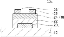
図1に示す有機薄膜トランジスタ10aは、支持体12と、支持体12上に形成されたトランジスタ素子18と、を有して構成される。
有機 The organic thin film transistor 10 a shown in FIG. 1 includes a support 12 and a transistor element 18 formed on the support 12.
トランジスタ素子18は、支持体12の表面に形成されたゲート電極20と、ゲート電極20を包含するように形成された無機膜(絶縁膜)22と、無機膜22上に形成された有機半導体層24と、有機半導体層24上にそれぞれ離間して形成されるソース電極26およびドレイン電極28と、を有する。すなわち、トランジスタ素子18は、いわゆるボトムゲート-トップコンタクト型のトランジスタ素子である。
なお、以下の説明において、便宜的に支持体12側を下側、ソース電極26およびドレイン電極28側を上側として説明を行う。 Thetransistor element 18 includes a gate electrode 20 formed on the surface of the support 12, an inorganic film (insulating film) 22 formed to cover the gate electrode 20, and an organic semiconductor layer formed on the inorganic film 22. 24, and a source electrode 26 and a drain electrode 28 formed separately on the organic semiconductor layer 24. That is, the transistor element 18 is a so-called bottom gate-top contact type transistor element.
In the following description, thesupport 12 side will be described as a lower side and the source electrode 26 and the drain electrode 28 side as an upper side for convenience.
なお、以下の説明において、便宜的に支持体12側を下側、ソース電極26およびドレイン電極28側を上側として説明を行う。 The
In the following description, the
ここで、本発明において、絶縁膜は、SiNH(水素化窒化ケイ素)からなる無機膜を含む。図1に示す例では、SiNHからなる無機膜22が絶縁膜である。
SiNHからなる無機膜(以下、SiNH膜ともいう)22は、従来の有機薄膜トランジスタで絶縁膜として用いられているSiO(酸化ケイ素)膜、SiN(窒化ケイ素)膜等の無機膜と比較して柔軟性に優れている。また、SiNH膜は、柔軟性に優れており割れにくいためクラック等による絶縁性の低下も起きにくい。そのため、本発明の有機薄膜トランジスタは、絶縁膜として、SiNHからなる無機膜22を用いることで、絶縁膜を絶縁性に優れ、かつ、柔軟性に優れるものとすることができる。これによって、有機薄膜トランジスタとして屈曲性を高くすることができ、また、絶縁膜のピンホールおよび平面性等に起因するキャリア移動度の低下を抑制できる。 Here, in the present invention, the insulating film includes an inorganic film made of SiNH (silicon hydronitride). In the example shown in FIG. 1, theinorganic film 22 made of SiNH is an insulating film.
Theinorganic film 22 made of SiNH (hereinafter also referred to as SiNH film) is more flexible than inorganic films such as SiO (silicon oxide) film and SiN (silicon nitride) film used as an insulating film in a conventional organic thin film transistor. Excellent in nature. Further, the SiNH film is excellent in flexibility and hard to be broken, so that the insulating property due to cracks or the like is hardly reduced. Therefore, in the organic thin film transistor of the present invention, by using the inorganic film 22 made of SiNH as the insulating film, the insulating film can have excellent insulating properties and excellent flexibility. As a result, the flexibility of the organic thin film transistor can be increased, and a decrease in carrier mobility due to pinholes and flatness of the insulating film can be suppressed.
SiNHからなる無機膜(以下、SiNH膜ともいう)22は、従来の有機薄膜トランジスタで絶縁膜として用いられているSiO(酸化ケイ素)膜、SiN(窒化ケイ素)膜等の無機膜と比較して柔軟性に優れている。また、SiNH膜は、柔軟性に優れており割れにくいためクラック等による絶縁性の低下も起きにくい。そのため、本発明の有機薄膜トランジスタは、絶縁膜として、SiNHからなる無機膜22を用いることで、絶縁膜を絶縁性に優れ、かつ、柔軟性に優れるものとすることができる。これによって、有機薄膜トランジスタとして屈曲性を高くすることができ、また、絶縁膜のピンホールおよび平面性等に起因するキャリア移動度の低下を抑制できる。 Here, in the present invention, the insulating film includes an inorganic film made of SiNH (silicon hydronitride). In the example shown in FIG. 1, the
The
ここで、SiNH膜22中のSiNとHとの原子数の比率SiN:Hは、1:0.7~2であるのが好ましく、1:0.8~1.8であるのがより好ましく、1:0.9~1.5であるのがさらに好ましい。
SiNH膜22中のHの比率が高いと膜の緻密さが低下するため屈曲性は高くなる。一方、Hの比率が高すぎると膜の緻密さが低くなりすぎて、絶縁性が低くなるおそれがある。これに対して、SiNとHとの原子数の比率SiN:Hを上記範囲とすることで、屈曲性と絶縁性を両立することができる。 Here, the ratio SiN: H of the number of atoms of SiN and H in theSiNH film 22 is preferably 1: 0.7 to 2, and more preferably 1: 0.8 to 1.8. , 1: 0.9-1.5.
When the ratio of H in theSiNH film 22 is high, the flexibility of the film is increased because the film density is reduced. On the other hand, if the ratio of H is too high, the denseness of the film becomes too low, and the insulating property may be lowered. On the other hand, by setting the ratio of the number of atoms between SiN and H, SiN: H, within the above range, both flexibility and insulation can be achieved.
SiNH膜22中のHの比率が高いと膜の緻密さが低下するため屈曲性は高くなる。一方、Hの比率が高すぎると膜の緻密さが低くなりすぎて、絶縁性が低くなるおそれがある。これに対して、SiNとHとの原子数の比率SiN:Hを上記範囲とすることで、屈曲性と絶縁性を両立することができる。 Here, the ratio SiN: H of the number of atoms of SiN and H in the
When the ratio of H in the
SiNとHとの原子数の比率は、RBS/HFS法(Rutherford Backscattering Spectrometry/Hydrogen Forward scattering Spectrometry(ラザフォード後方散乱分析/水素前方散乱分析法))を利用して測定できる。
具体的には、RBS/HFS法によって、SiNH膜22の厚さ方向の全域においてケイ素、水素、および、窒素の各原子の量(数)を検出して、原子数の比率を算出すればよい。
あるいは、XPS測定(X線光電子分光測定)により、SiNH膜22の表面におけるSi、N、Hの原子数を測定し、これからSiNとH原子の比率として算出することもできる。 The ratio of the number of atoms between SiN and H can be measured using the RBS / HFS method (Rutherford Backscattering Spectrometry / Hydrogen Forward scattering Spectrometry).
More specifically, the ratio of the number of atoms may be calculated by detecting the amounts (numbers) of the respective atoms of silicon, hydrogen, and nitrogen in the entire region in the thickness direction of theSiNH film 22 by the RBS / HFS method. .
Alternatively, the number of Si, N, and H atoms on the surface of theSiNH film 22 can be measured by XPS measurement (X-ray photoelectron spectroscopy measurement), and can be calculated as the ratio between SiN and H atoms.
具体的には、RBS/HFS法によって、SiNH膜22の厚さ方向の全域においてケイ素、水素、および、窒素の各原子の量(数)を検出して、原子数の比率を算出すればよい。
あるいは、XPS測定(X線光電子分光測定)により、SiNH膜22の表面におけるSi、N、Hの原子数を測定し、これからSiNとH原子の比率として算出することもできる。 The ratio of the number of atoms between SiN and H can be measured using the RBS / HFS method (Rutherford Backscattering Spectrometry / Hydrogen Forward scattering Spectrometry).
More specifically, the ratio of the number of atoms may be calculated by detecting the amounts (numbers) of the respective atoms of silicon, hydrogen, and nitrogen in the entire region in the thickness direction of the
Alternatively, the number of Si, N, and H atoms on the surface of the
また、屈曲性の観点では、SiNH膜22は薄いほど好ましい。一方、絶縁性の観点では、SiNH膜22はある程度の厚みが必要である。以上の観点から、SiNH膜22の厚みは、1nm~100nmであるのが好ましく、5nm~80nmであるのがより好ましく、10nm~50nmであるのがさらに好ましい。
From the viewpoint of flexibility, the thinner the SiNH film 22, the more preferable. On the other hand, from the viewpoint of insulating properties, the SiNH film 22 needs to have a certain thickness. From the above viewpoints, the thickness of the SiNH film 22 is preferably 1 nm to 100 nm, more preferably 5 nm to 80 nm, and still more preferably 10 nm to 50 nm.
ここで、図1に示す例では、ゲート電極20の上に直接、SiNH膜22が積層された構成としたがこれに限定はされず、ゲート電極20とSiNH膜22との間に他の層を有していてもよい。
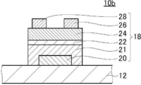
例えば、図2に示す有機薄膜トランジスタ10bは、支持体12の表面に形成されたゲート電極20と、ゲート電極20を包含するように形成された有機層21と、有機層21の上に形成されたSiNH膜22と、SiNH膜22上に形成された有機半導体層24と、有機半導体層24上にそれぞれ離間して形成されるソース電極26およびドレイン電極28と、を有する。 Here, in the example shown in FIG. 1, the structure in which theSiNH film 22 is directly laminated on the gate electrode 20 is not limited to this, and another layer is provided between the gate electrode 20 and the SiNH film 22. May be provided.
For example, the organicthin film transistor 10 b shown in FIG. 2 is formed on the gate electrode 20 formed on the surface of the support 12, the organic layer 21 formed so as to include the gate electrode 20, and formed on the organic layer 21. It has a SiNH film 22, an organic semiconductor layer 24 formed on the SiNH film 22, and a source electrode 26 and a drain electrode 28 formed separately on the organic semiconductor layer 24.
例えば、図2に示す有機薄膜トランジスタ10bは、支持体12の表面に形成されたゲート電極20と、ゲート電極20を包含するように形成された有機層21と、有機層21の上に形成されたSiNH膜22と、SiNH膜22上に形成された有機半導体層24と、有機半導体層24上にそれぞれ離間して形成されるソース電極26およびドレイン電極28と、を有する。 Here, in the example shown in FIG. 1, the structure in which the
For example, the organic
有機層21はSiNH膜22の下地となる層である。後述するが、SiNH膜22は、好ましくは、プラズマCVD(Chemical Vapor Deposition)によって形成される。SiNH膜22をプラズマCVDで形成する場合には、SiNH膜22を導体であるゲート電極20の上に直接形成することは難しい。
The organic layer 21 is a layer serving as a base of the SiNH film 22. As will be described later, the SiNH film 22 is preferably formed by plasma CVD (Chemical Vapor Deposition). When the SiNH film 22 is formed by plasma CVD, it is difficult to form the SiNH film 22 directly on the gate electrode 20 which is a conductor.
これに対して、ゲート電極20の上に有機層21を設けることで、SiNH膜22をプラズマCVDで形成することができる。また、有機層21は、SiNH膜22の形成面の凹凸および表面に付着する異物等を包埋する。その結果、SiNH膜22の形成面を適正にして、均一な厚みでピンホール等のないSiNH膜22を適正に形成することを可能にする。
In contrast, by providing the organic layer 21 on the gate electrode 20, the SiNH film 22 can be formed by plasma CVD. In addition, the organic layer 21 embeds irregularities on the surface on which the SiNH film 22 is formed and foreign substances adhering to the surface. As a result, the surface on which the SiNH film 22 is formed is made appropriate, and the SiNH film 22 having a uniform thickness and no pinholes can be formed properly.
また、後述するように、SiNH膜22は転写によってゲート電極20の上に積層して形成することができる。この場合は、基板を剥離可能な転写型の積層フィルム(図7参照)を作製し、転写型積層フィルムから基板を剥離してSiNH膜22を含む転写層をゲート電極20上に転写する。転写型積層フィルムにおいて、転写層を基板から剥離可能にするために、SiNH膜22は、基板の上に形成された有機層21上に形成されている。この有機層21側をゲート電極20側に向けて転写することで図2に示す構成の有機薄膜トランジスタとすることができる。
As described later, the SiNH film 22 can be formed by being stacked on the gate electrode 20 by transfer. In this case, a transfer-type laminated film (see FIG. 7) from which the substrate can be peeled off is prepared, the substrate is peeled off from the transfer-type laminated film, and the transfer layer including the SiNH film 22 is transferred onto the gate electrode 20. In the transfer type laminated film, the SiNH film 22 is formed on the organic layer 21 formed on the substrate so that the transfer layer can be peeled from the substrate. The organic thin film transistor having the configuration shown in FIG. 2 can be obtained by transferring the organic layer 21 toward the gate electrode 20.
SiNH膜22を転写によって形成する構成とすることで、支持体12およびゲート電極20の構成によらず、SiNH膜22をプラズマCVD等の所望の方法、条件で形成することが可能となる。
With the configuration in which the SiNH film 22 is formed by transfer, the SiNH film 22 can be formed by a desired method and conditions such as plasma CVD regardless of the configurations of the support 12 and the gate electrode 20.
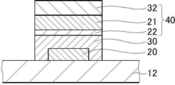
また、本発明の有機薄膜トランジスタは、図3に示す有機薄膜トランジスタ10cのように、支持体12の表面に形成されたゲート電極20と、ゲート電極20を包含するように形成された接着層30と、接着層30の上に形成されたSiNH膜22と、SiNH膜22上に形成された有機層21と、有機層21上に形成された有機半導体層24と、有機半導体層24上にそれぞれ離間して形成されるソース電極26およびドレイン電極28と、を有する構成としてもよい。
Further, the organic thin film transistor of the present invention includes a gate electrode 20 formed on the surface of the support 12 and an adhesive layer 30 formed so as to include the gate electrode 20, as in the organic thin film transistor 10c shown in FIG. The SiNH film 22 formed on the adhesive layer 30, the organic layer 21 formed on the SiNH film 22, the organic semiconductor layer 24 formed on the organic layer 21, and the organic semiconductor layer 24 And a source electrode 26 and a drain electrode 28 that are formed.
SiNH膜22を転写によってゲート電極20の上に積層する場合は、転写型積層フィルムのSiNH膜22側を接着層30を介して貼り合わせて、その後、転写型積層フィルムの基板を転写層から剥離することで、SiNH膜22をゲート電極20の上に積層することもできる。この場合、図3に示すように、絶縁膜であるSiNH膜22が接着層30と有機層21とに挟まれた構成となる。
When the SiNH film 22 is laminated on the gate electrode 20 by transfer, the transfer type laminated film is bonded to the SiNH film 22 side via the adhesive layer 30, and then the substrate of the transfer type laminated film is separated from the transfer layer. By doing so, the SiNH film 22 can be stacked on the gate electrode 20. In this case, as shown in FIG. 3, the configuration is such that the SiNH film 22 as an insulating film is sandwiched between the adhesive layer 30 and the organic layer 21.
なお、有機層21はSiNH膜22の下地となる層であり、SiNH膜22の形成面の凹凸等を包埋して適正にできればよく、絶縁性は有していなくてもよい。
同様に、接着層30は、SiNH膜22を含む転写層をゲート電極20上に貼合することができればよく、絶縁性は有していなくてもよい。 Note that theorganic layer 21 is a layer serving as a base of the SiNH film 22, and it is sufficient that the organic layer 21 can be properly formed by embedding irregularities and the like on the surface on which the SiNH film 22 is formed, and does not have to have insulating properties.
Similarly, theadhesive layer 30 only needs to be able to bond the transfer layer including the SiNH film 22 onto the gate electrode 20, and does not need to have insulating properties.
同様に、接着層30は、SiNH膜22を含む転写層をゲート電極20上に貼合することができればよく、絶縁性は有していなくてもよい。 Note that the
Similarly, the
また、SiNH膜22の下地層となる有機層21を有する構成の場合には、SiNH膜22と有機層21との組み合わせを2以上有していてもよい。すなわち、例えば、ゲート電極20の上に有機層21、SiNH膜22、有機層21、SiNH膜22のように有機層およびSiNH膜を2層以上有する構成としてもよい。
{Circle around (2)} In the case of the configuration having the organic layer 21 serving as the underlayer of the SiNH film 22, two or more combinations of the SiNH film 22 and the organic layer 21 may be provided. That is, for example, a configuration having two or more organic layers and SiNH films such as the organic layer 21, the SiNH film 22, the organic layer 21, and the SiNH film 22 on the gate electrode 20 may be adopted.
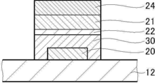
また、図1に示す例では、絶縁膜はSiNHからなる無機膜22を有する構成としたが、これに限定はされず、他の層を有していてもよい。
例えば、図4に示す有機薄膜トランジスタ10dは、絶縁膜として、SiNHからなる無機膜22と、第2の無機膜23とを有する。なお、有機薄膜トランジスタ10dは第2の無機膜23を有する以外は、図1に示す有機薄膜トランジスタ10aと同様の構成を有する。 Further, in the example shown in FIG. 1, the insulating film has a configuration including theinorganic film 22 made of SiNH. However, the present invention is not limited to this, and may have another layer.
For example, the organicthin film transistor 10d illustrated in FIG. 4 includes an inorganic film 22 made of SiNH and a second inorganic film 23 as insulating films. Note that the organic thin film transistor 10d has the same configuration as the organic thin film transistor 10a shown in FIG. 1 except that the organic thin film transistor 10d has the second inorganic film 23.
例えば、図4に示す有機薄膜トランジスタ10dは、絶縁膜として、SiNHからなる無機膜22と、第2の無機膜23とを有する。なお、有機薄膜トランジスタ10dは第2の無機膜23を有する以外は、図1に示す有機薄膜トランジスタ10aと同様の構成を有する。 Further, in the example shown in FIG. 1, the insulating film has a configuration including the
For example, the organic
第2の無機膜23は、SiO(酸化ケイ素)膜、SiN(窒化ケイ素)膜等の公知の無機膜とすることができる。第2の無機膜23を有することにより、高い絶縁性を得ることができる。その際、SiNH膜22を有するので、第2の無機膜23は薄くても絶縁性を確保でき、屈曲性も損なわない。
The second inorganic film 23 can be a known inorganic film such as a SiO (silicon oxide) film or a SiN (silicon nitride) film. By having the second inorganic film 23, high insulating properties can be obtained. At this time, since the second inorganic film 23 is thin, the insulating property can be ensured and the flexibility is not impaired because of the presence of the SiNH film 22.
また、第2の無機膜23として、SiNH膜22の有機半導体層24側(以下、表層ともいう)に、SiO2膜を有することが好ましい。SiNH膜22の表層にSiO2膜を有することで、SAM(self-assemble monolayer)等の有機半導体を形成する面に対して行われている従来公知の表面処理を行うことができる。これによって、絶縁膜の表面上で結晶性の高い有機半導体層が形成されやすくなり、有機薄膜トランジスタの性能を向上できる。
なお、第2の無機膜23としてSiO2膜、および、SiN膜等のケイ素化合物膜を形成する場合には、SiNH膜22と第2の無機膜23とは明確な界面を有するように別の層として形成されていてもよいし、SiNH膜22の表層においてSiO2の割合が高くなるように、一つの層として形成されていてもよい。 Further, as the secondinorganic film 23, it is preferable to have a SiO 2 film on the organic semiconductor layer 24 side (hereinafter also referred to as a surface layer) of the SiNH film 22. By providing a SiO 2 film on the surface of the SiNH film 22, a conventionally known surface treatment performed on a surface on which an organic semiconductor such as a SAM (self-assemble monolayer) is formed can be performed. Accordingly, an organic semiconductor layer having high crystallinity is easily formed on the surface of the insulating film, and the performance of the organic thin film transistor can be improved.
When a SiO 2 film or a silicon compound film such as a SiN film is formed as the secondinorganic film 23, another SiNH film 22 and a second inorganic film 23 are formed so as to have a clear interface. It may be formed as a layer, or may be formed as one layer so that the ratio of SiO 2 in the surface layer of the SiNH film 22 is increased.
なお、第2の無機膜23としてSiO2膜、および、SiN膜等のケイ素化合物膜を形成する場合には、SiNH膜22と第2の無機膜23とは明確な界面を有するように別の層として形成されていてもよいし、SiNH膜22の表層においてSiO2の割合が高くなるように、一つの層として形成されていてもよい。 Further, as the second
When a SiO 2 film or a silicon compound film such as a SiN film is formed as the second
表面処理の効果を十分に得られる観点から、SiO2膜の厚みは0.1nm~5nmが好ましく、0.2nm~3nmがより好ましく、0.1nm~1nmがさらに好ましい。
From the viewpoint of sufficiently obtaining the effect of the surface treatment, the thickness of the SiO 2 film is preferably 0.1 nm to 5 nm, more preferably 0.2 nm to 3 nm, and still more preferably 0.1 nm to 1 nm.
以下、有機薄膜トランジスタを構成する部位について詳細に説明する。
<支持体>
支持体12は、各種の有機薄膜トランジスタにおいて支持体として利用される、公知のシート状物(フィルム、板状物)を用いることができる。 Hereinafter, the parts constituting the organic thin film transistor will be described in detail.
<Support>
As thesupport 12, a known sheet-like material (film, plate-like material) used as a support in various organic thin film transistors can be used.
<支持体>
支持体12は、各種の有機薄膜トランジスタにおいて支持体として利用される、公知のシート状物(フィルム、板状物)を用いることができる。 Hereinafter, the parts constituting the organic thin film transistor will be described in detail.
<Support>
As the
支持体12の材料には、制限はなく、トランジスタ素子18を形成可能であれば、各種の材料が利用可能である。支持体12の材料としては、プラスチック材料、シリコン材料、ガラス材料、石英、および、セラミック材料等が挙げられる。中でも、各デバイスへの適用性及びコストの観点から、ガラス材料又はプラスチック材料であることが好ましい。
プラスチック材料としては、ポリエチレンナフタレート(PEN)、ポリエチレンテレフタレート(PET)などのポリエステルフィルム、シクロオレフィンポリマーフィルム、ポリカーボネートフィルム、トリアセチルセルロース(TAC)フィルム、ポリイミドフィルムが例示される。また、これらプラスチックフィルムをガラスに貼り合わせたものを用いることもできる。 The material of thesupport 12 is not limited, and various materials can be used as long as the transistor element 18 can be formed. Examples of the material of the support 12 include a plastic material, a silicon material, a glass material, quartz, and a ceramic material. Among them, a glass material or a plastic material is preferable from the viewpoint of applicability to each device and cost.
Examples of the plastic material include polyester films such as polyethylene naphthalate (PEN) and polyethylene terephthalate (PET), cycloolefin polymer films, polycarbonate films, triacetyl cellulose (TAC) films, and polyimide films. Further, those obtained by bonding these plastic films to glass can also be used.
プラスチック材料としては、ポリエチレンナフタレート(PEN)、ポリエチレンテレフタレート(PET)などのポリエステルフィルム、シクロオレフィンポリマーフィルム、ポリカーボネートフィルム、トリアセチルセルロース(TAC)フィルム、ポリイミドフィルムが例示される。また、これらプラスチックフィルムをガラスに貼り合わせたものを用いることもできる。 The material of the
Examples of the plastic material include polyester films such as polyethylene naphthalate (PEN) and polyethylene terephthalate (PET), cycloolefin polymer films, polycarbonate films, triacetyl cellulose (TAC) films, and polyimide films. Further, those obtained by bonding these plastic films to glass can also be used.
基板の厚みは、特に限定されない。例えば、10mm以下であるのが好ましく、2mm以下であるのが更に好ましく、1.5mm以下であるのが特に好ましい。一方、0.01mm以上であるのが好ましく、0.05mm以上であるのが更に好ましい。
厚 み The thickness of the substrate is not particularly limited. For example, it is preferably 10 mm or less, more preferably 2 mm or less, and particularly preferably 1.5 mm or less. On the other hand, it is preferably at least 0.01 mm, more preferably at least 0.05 mm.
<ゲート電極>
ゲート電極20は、有機薄膜トランジスタのゲート電極として用いられている従来公知の電極を用いることができる。
ゲート電極を構成する導電性材料(電極材料ともいう)としては、特に限定されない。例えば、白金、金、銀、アルミニウム、クロム、ニッケル、銅、モリブデン、チタン、マグネシウム、カルシウム、バリウム、ナトリウム、パラジウム、鉄、マンガン等の金属;InO2、SnO2、インジウム・錫酸化物(ITO)、フッ素ドープ酸化錫(FTO)、アルミニウムドープ酸化亜鉛(AZO)、ガリウムドープ酸化亜鉛(GZO)等の導電性金属酸化物;ポリアニリン、ポリピロール、ポリチオフェン、ポリアセチレン、ポリ(3,4-エチレンジオキシチオフェン)/ポリスチレンスルホン酸(PEDOT/PSS)等の導電性高分子;塩酸、硫酸、スルホン酸等の酸、PF6、AsF5、FeCl3等のルイス酸、ヨウ素等のハロゲン原子、ナトリウム、カリウム等の金属原子等のドーパントを添加した上記導電性高分子、並びに、カーボンブラック、グラファイト粉、金属微粒子等を分散した導電性の複合材料等が挙げられる。これらの材料は、1種のみを用いても、2種以上を任意の組み合わせ及び比率で併用してもよい。
また、ゲート電極は、上記導電性材料からなる1層でもよく、2層以上を積層してもよい。 <Gate electrode>
As thegate electrode 20, a conventionally known electrode used as a gate electrode of an organic thin film transistor can be used.
The conductive material (also referred to as an electrode material) forming the gate electrode is not particularly limited. For example, metals such as platinum, gold, silver, aluminum, chromium, nickel, copper, molybdenum, titanium, magnesium, calcium, barium, sodium, palladium, iron, and manganese; InO 2 , SnO 2 , indium tin oxide (ITO) ), Conductive metal oxides such as fluorine-doped tin oxide (FTO), aluminum-doped zinc oxide (AZO), and gallium-doped zinc oxide (GZO); polyaniline, polypyrrole, polythiophene, polyacetylene, poly (3,4-ethylenedioxy) Conductive polymers such as thiophene) / polystyrenesulfonic acid (PEDOT / PSS); acids such as hydrochloric acid, sulfuric acid and sulfonic acid; Lewis acids such as PF 6 , AsF 5 and FeCl 3 ; halogen atoms such as iodine; sodium and potassium The above-mentioned conductive polymer added with a dopant such as a metal atom such as , As well as carbon black, graphite powder, a composite material of the conductive dispersed metal fine particles and the like. One of these materials may be used alone, or two or more thereof may be used in an optional combination and ratio.
The gate electrode may be a single layer made of the above conductive material, or may be a stack of two or more layers.
ゲート電極20は、有機薄膜トランジスタのゲート電極として用いられている従来公知の電極を用いることができる。
ゲート電極を構成する導電性材料(電極材料ともいう)としては、特に限定されない。例えば、白金、金、銀、アルミニウム、クロム、ニッケル、銅、モリブデン、チタン、マグネシウム、カルシウム、バリウム、ナトリウム、パラジウム、鉄、マンガン等の金属;InO2、SnO2、インジウム・錫酸化物(ITO)、フッ素ドープ酸化錫(FTO)、アルミニウムドープ酸化亜鉛(AZO)、ガリウムドープ酸化亜鉛(GZO)等の導電性金属酸化物;ポリアニリン、ポリピロール、ポリチオフェン、ポリアセチレン、ポリ(3,4-エチレンジオキシチオフェン)/ポリスチレンスルホン酸(PEDOT/PSS)等の導電性高分子;塩酸、硫酸、スルホン酸等の酸、PF6、AsF5、FeCl3等のルイス酸、ヨウ素等のハロゲン原子、ナトリウム、カリウム等の金属原子等のドーパントを添加した上記導電性高分子、並びに、カーボンブラック、グラファイト粉、金属微粒子等を分散した導電性の複合材料等が挙げられる。これらの材料は、1種のみを用いても、2種以上を任意の組み合わせ及び比率で併用してもよい。
また、ゲート電極は、上記導電性材料からなる1層でもよく、2層以上を積層してもよい。 <Gate electrode>
As the
The conductive material (also referred to as an electrode material) forming the gate electrode is not particularly limited. For example, metals such as platinum, gold, silver, aluminum, chromium, nickel, copper, molybdenum, titanium, magnesium, calcium, barium, sodium, palladium, iron, and manganese; InO 2 , SnO 2 , indium tin oxide (ITO) ), Conductive metal oxides such as fluorine-doped tin oxide (FTO), aluminum-doped zinc oxide (AZO), and gallium-doped zinc oxide (GZO); polyaniline, polypyrrole, polythiophene, polyacetylene, poly (3,4-ethylenedioxy) Conductive polymers such as thiophene) / polystyrenesulfonic acid (PEDOT / PSS); acids such as hydrochloric acid, sulfuric acid and sulfonic acid; Lewis acids such as PF 6 , AsF 5 and FeCl 3 ; halogen atoms such as iodine; sodium and potassium The above-mentioned conductive polymer added with a dopant such as a metal atom such as , As well as carbon black, graphite powder, a composite material of the conductive dispersed metal fine particles and the like. One of these materials may be used alone, or two or more thereof may be used in an optional combination and ratio.
The gate electrode may be a single layer made of the above conductive material, or may be a stack of two or more layers.
ゲート電極の形成方法に制限は無い。例えば、真空蒸着法等の物理蒸着法(PVD)、化学蒸着法(CVD法)、スパッタ法、印刷法(塗布法)、転写法、ゾルゲル法、メッキ法等により形成された膜を、必要に応じて所望の形状にパターンニングする方法が挙げられる。
塗布法では、上記材料の溶液、ペースト又は分散液を調製、塗布し、乾燥、焼成、光硬化又はエージング等により、膜を形成し、又は直接電極を形成できる。
また、インクジェット印刷、スクリーン印刷、(反転)オフセット印刷、凸版印刷、凹版印刷、平版印刷、熱転写印刷、マイクロコンタクトプリンティング法等は、所望のパターニングが可能であり、工程の簡素化、コスト低減、高速化の点で好ましい。
スピンコート法、ダイコート法、マイクログラビアコート法、ディップコート法を採用する場合も、下記フォトリソグラフィー法等と組み合わせてパターニングすることができる。 There is no limitation on the method for forming the gate electrode. For example, a film formed by a physical vapor deposition method (PVD) such as a vacuum vapor deposition method, a chemical vapor deposition method (CVD method), a sputtering method, a printing method (coating method), a transfer method, a sol-gel method, or a plating method is required. There is a method of patterning a desired shape according to the method.
In the application method, a solution, a paste, or a dispersion of the above materials is prepared and applied, and a film is formed by drying, baking, photocuring, aging, or the like, or an electrode can be directly formed.
In addition, inkjet printing, screen printing, (reverse) offset printing, letterpress printing, intaglio printing, lithographic printing, thermal transfer printing, microcontact printing, etc., can perform desired patterning, simplifying the process, reducing costs, and increasing speed. It is preferable in terms of conversion.
Even when a spin coating method, a die coating method, a microgravure coating method, or a dip coating method is adopted, patterning can be performed in combination with the following photolithography method or the like.
フォトリソグラフィー法としては、例えば、フォトレジストのパターニングと、エッチング液によるウェットエッチングや反応性のプラズマによるドライエッチング等のエッチングやリフトオフ法等とを組み合わせる方法等が挙げられる。
他のパターニング方法として、上記材料に、レーザーや電子線等のエネルギー線を照射して、研磨し、又は材料の導電性を変化させる方法も挙げられる。
さらに、支持体以外の基板に印刷したゲート電極用組成物を転写させる方法も挙げられる。 Examples of the photolithography method include a method of combining patterning of a photoresist with etching such as wet etching with an etchant or dry etching with reactive plasma, a lift-off method, and the like.
As another patterning method, a method of irradiating the above-mentioned material with an energy beam such as a laser or an electron beam to polish or change the conductivity of the material may be used.
Furthermore, there is a method of transferring the composition for a gate electrode printed on a substrate other than the support.
ゲート電極20の厚みは、任意であるが、1nm以上が好ましく、10nm以上が特に好ましい。また、500nm以下が好ましく、200nm以下が特に好ましい。
The thickness of the gate electrode 20 is arbitrary, but is preferably 1 nm or more, and particularly preferably 10 nm or more. Further, it is preferably at most 500 nm, particularly preferably at most 200 nm.
<ソース電極、ドレイン電極>
ソース電極26は、有機薄膜トランジスタにおいて、配線を通じて外部から電流が流入する電極である。また、ドレイン電極28は、配線を通じて外部に電流を送り出す電極であり、通常、有機半導体層24に接して設けられる。
ソース電極及びドレイン電極の材料としては、従来の有機薄膜トランジスタに用いられている導電性材料を用いることができ、例えば、上記ゲート電極で説明した導電性材料等が挙げられる <Source electrode, drain electrode>
Thesource electrode 26 is an electrode in the organic thin film transistor through which a current flows from the outside through a wiring. Further, the drain electrode 28 is an electrode for sending a current to the outside through a wiring, and is usually provided in contact with the organic semiconductor layer 24.
As a material for the source electrode and the drain electrode, a conductive material used for a conventional organic thin film transistor can be used, and examples thereof include the conductive materials described for the gate electrode.
ソース電極26は、有機薄膜トランジスタにおいて、配線を通じて外部から電流が流入する電極である。また、ドレイン電極28は、配線を通じて外部に電流を送り出す電極であり、通常、有機半導体層24に接して設けられる。
ソース電極及びドレイン電極の材料としては、従来の有機薄膜トランジスタに用いられている導電性材料を用いることができ、例えば、上記ゲート電極で説明した導電性材料等が挙げられる <Source electrode, drain electrode>
The
As a material for the source electrode and the drain electrode, a conductive material used for a conventional organic thin film transistor can be used, and examples thereof include the conductive materials described for the gate electrode.
ソース電極及びドレイン電極は、それぞれ、上記ゲート電極の形成方法と同様の方法により形成することができる。
The source electrode and the drain electrode can each be formed by a method similar to the method of forming the gate electrode.
上記フォトリソグラフィー法としては、リフトオフ法又はエッチング法を採用できる。
特に、ソース電極及びドレイン電極はエッチング法でも好適に形成することができる。エッチング法は、導電性材料を成膜した後に不要部分をエッチングにより除去する方法である。エッチング法によりパターニングすると、レジスト除去時に下地に残った導電性材料の剥がれ、レジスト残渣や除去された導電性材料の下地への再付着を防止でき、電極エッジ部の形状に優れる。この点で、リフトオフ法よりも好ましい。 As the photolithography method, a lift-off method or an etching method can be employed.
In particular, the source electrode and the drain electrode can be suitably formed by an etching method. The etching method is a method of removing unnecessary portions by etching after forming a conductive material. When patterning is performed by the etching method, the conductive material remaining on the base at the time of removing the resist can be peeled off, and the resist residue and the removed conductive material can be prevented from reattaching to the base, and the shape of the electrode edge portion is excellent. In this respect, it is preferable to the lift-off method.
リフトオフ法は、下地の一部にレジストを塗布し、この上に導電性材料を成膜し、レジスト等を溶媒により溶出又は剥離等することにより、レジスト上の導電性材料ごと除去して、レジストが塗布されていなかった部分にのみ導電性材料の膜を形成する方法である。
In the lift-off method, a resist is applied to a part of a base, a conductive material is formed thereon, and the resist or the like is removed or removed by eluting or peeling off the resist with a solvent. Is a method of forming a film of a conductive material only on a portion to which no has been applied.
ソース電極26及びドレイン電極28の厚みは、任意であるが、それぞれ、1nm以上が好ましく、10nm以上が特に好ましい。また、500nm以下が好ましく、300nm以下が特に好ましい。
The thickness of the source electrode 26 and the drain electrode 28 is arbitrary, but is preferably 1 nm or more, and particularly preferably 10 nm or more. Further, it is preferably at most 500 nm, particularly preferably at most 300 nm.
<有機半導体層>
有機半導体層24は、半導体性を示し、キャリアを蓄積可能な層である。有機半導体層24は、有機半導体を含有する層であればよい。
有機半導体としては、特に限定されず、有機ポリマー及びその誘導体、低分子化合物等が挙げられる。
本発明において、低分子化合物は、有機ポリマー及びその誘導体以外の化合物を意味する。すなわち、繰り返し単位を有さない化合物をいう。低分子化合物は、このような化合物である限り、分子量は特に限定されるものではない。低分子化合物の分子量は、好ましくは300~2000であり、さらに好ましくは400~1000である。 <Organic semiconductor layer>
Theorganic semiconductor layer 24 is a layer having semiconductor properties and capable of storing carriers. The organic semiconductor layer 24 may be a layer containing an organic semiconductor.
The organic semiconductor is not particularly limited, and examples thereof include an organic polymer and a derivative thereof, and a low-molecular compound.
In the present invention, the low molecular compound means a compound other than the organic polymer and its derivative. That is, it refers to a compound having no repeating unit. The molecular weight of the low molecular weight compound is not particularly limited as long as it is such a compound. The molecular weight of the low molecular weight compound is preferably from 300 to 2,000, more preferably from 400 to 1,000.
有機半導体層24は、半導体性を示し、キャリアを蓄積可能な層である。有機半導体層24は、有機半導体を含有する層であればよい。
有機半導体としては、特に限定されず、有機ポリマー及びその誘導体、低分子化合物等が挙げられる。
本発明において、低分子化合物は、有機ポリマー及びその誘導体以外の化合物を意味する。すなわち、繰り返し単位を有さない化合物をいう。低分子化合物は、このような化合物である限り、分子量は特に限定されるものではない。低分子化合物の分子量は、好ましくは300~2000であり、さらに好ましくは400~1000である。 <Organic semiconductor layer>
The
The organic semiconductor is not particularly limited, and examples thereof include an organic polymer and a derivative thereof, and a low-molecular compound.
In the present invention, the low molecular compound means a compound other than the organic polymer and its derivative. That is, it refers to a compound having no repeating unit. The molecular weight of the low molecular weight compound is not particularly limited as long as it is such a compound. The molecular weight of the low molecular weight compound is preferably from 300 to 2,000, more preferably from 400 to 1,000.
有機半導体層24の材料としては、特開2015-170760号公報の段落[0063]~[0160]に記載の材料が例示される。また、有機半導体層24の材料として、特開2015-195361に記載の有機半導体、特開2018-006745号に記載の有機半導体も例示される。
材料 Examples of the material of the organic semiconductor layer 24 include the materials described in paragraphs [0063] to [0160] of JP-A-2015-170760. Further, examples of the material of the organic semiconductor layer 24 include an organic semiconductor described in JP-A-2015-195361 and an organic semiconductor described in JP-A-2018-006745.
有機半導体層24の形成方法は特に限定はされず、従来公知の有機半導体層の形成方法が利用可能である。例えば、有機半導体層となる材料を溶媒に溶解してその溶液を絶縁膜上に塗布し、乾燥させることにより半導体活性層を形成する方法がある。
The method for forming the organic semiconductor layer 24 is not particularly limited, and a conventionally known method for forming an organic semiconductor layer can be used. For example, there is a method of forming a semiconductor active layer by dissolving a material to be an organic semiconductor layer in a solvent, applying the solution on an insulating film, and drying the solution.
有機半導体層24の厚みは、任意であるが、0.001μm以上が好ましく、0.01μm以上が特に好ましい。また、1μm以下が好ましく、0.5μm以下が特に好ましい。
(4) The thickness of the organic semiconductor layer 24 is arbitrary, but is preferably 0.001 μm or more, and particularly preferably 0.01 μm or more. Further, it is preferably 1 μm or less, particularly preferably 0.5 μm or less.
<無機膜(SiNH膜)>
SiNH膜22は、ゲート電極20と有機半導体層24との間に積層され、ゲート電極20と有機半導体層24とを絶縁する層である。 <Inorganic film (SiNH film)>
TheSiNH film 22 is laminated between the gate electrode 20 and the organic semiconductor layer 24 and is a layer that insulates the gate electrode 20 from the organic semiconductor layer 24.
SiNH膜22は、ゲート電極20と有機半導体層24との間に積層され、ゲート電極20と有機半導体層24とを絶縁する層である。 <Inorganic film (SiNH film)>
The
前述のとおり、絶縁膜としてSiNH膜22を用いることで、従来の有機薄膜トランジスタで絶縁膜として用いられているSiO(酸化ケイ素)膜、SiN(窒化ケイ素)膜等の無機膜と比較して柔軟性に優れた絶縁膜とすることができる。
As described above, by using the SiNH film 22 as the insulating film, flexibility is higher than that of an inorganic film such as a SiO (silicon oxide) film or a SiN (silicon nitride) film used as an insulating film in a conventional organic thin film transistor. It is possible to obtain an excellent insulating film.
なお、SiNH膜22を2層以上有する場合には、2層以上のSiNH膜22は、同じ組成比であってもよいし、異なる組成比であってもよい。また、厚みも同じであっても異なっていてもよい。
When two or more SiNH films 22 are provided, the two or more SiNH films 22 may have the same composition ratio or different composition ratios. Further, the thickness may be the same or different.
SiNH膜22は、材料に応じた公知の方法で形成できる。
例えば、CCP(Capacitively Coupled Plasma)-CVDおよびICP(Inductively Coupled Plasm)-CVD等のプラズマCVD、原子層堆積法(ALD(Atomic Layer Deposition))、マグネトロンスパッタリングおよび反応性スパッタリング等のスパッタリング、ならびに、真空蒸着などの各種の気相成膜法が好適に挙げられる。
中でも、CCP-CVDおよびICP-CVD等のプラズマCVDは、好適に利用される。 TheSiNH film 22 can be formed by a known method according to a material.
For example, plasma CVD such as CCP (Capacitively Coupled Plasma) -CVD and ICP (Inductively Coupled Plasm) -CVD, atomic layer deposition (ALD), sputtering such as magnetron sputtering and reactive sputtering, and vacuum Various vapor-phase film forming methods such as vapor deposition are preferably exemplified.
Among them, plasma CVD such as CCP-CVD and ICP-CVD are preferably used.
例えば、CCP(Capacitively Coupled Plasma)-CVDおよびICP(Inductively Coupled Plasm)-CVD等のプラズマCVD、原子層堆積法(ALD(Atomic Layer Deposition))、マグネトロンスパッタリングおよび反応性スパッタリング等のスパッタリング、ならびに、真空蒸着などの各種の気相成膜法が好適に挙げられる。
中でも、CCP-CVDおよびICP-CVD等のプラズマCVDは、好適に利用される。 The
For example, plasma CVD such as CCP (Capacitively Coupled Plasma) -CVD and ICP (Inductively Coupled Plasm) -CVD, atomic layer deposition (ALD), sputtering such as magnetron sputtering and reactive sputtering, and vacuum Various vapor-phase film forming methods such as vapor deposition are preferably exemplified.
Among them, plasma CVD such as CCP-CVD and ICP-CVD are preferably used.
<第2の無機膜>
第2の無機膜23は、無機化合物を含む薄膜である。第2の無機膜23は、絶縁性を発現する。また、第2の無機膜23を有することで、表面性状をSiNH膜とは異なるものとすることができ、有機半導体を形成する面に対して行われている従来公知の表面処理を行うことができる。 <Second inorganic film>
The secondinorganic film 23 is a thin film containing an inorganic compound. The second inorganic film 23 has an insulating property. In addition, by having the second inorganic film 23, the surface properties can be made different from those of the SiNH film, and a conventionally known surface treatment performed on a surface on which an organic semiconductor is formed can be performed. it can.
第2の無機膜23は、無機化合物を含む薄膜である。第2の無機膜23は、絶縁性を発現する。また、第2の無機膜23を有することで、表面性状をSiNH膜とは異なるものとすることができ、有機半導体を形成する面に対して行われている従来公知の表面処理を行うことができる。 <Second inorganic film>
The second
第2の無機膜23の材料には、制限はなく、絶縁性を発現する無機化合物からなる、公知の有機薄膜トランジスタに用いられる無機化合物が、各種、利用可能である。
第2の無機膜23の材料としては、例えば、酸化アルミニウム、酸化マグネシウム、酸化タンタル、酸化ジルコニウム、酸化チタン、酸化インジウムスズ(ITO)などの金属酸化物; 窒化アルミニウムなどの金属窒化物; 炭化アルミニウムなどの金属炭化物; 酸化ケイ素、酸化窒化ケイ素、酸炭化ケイ素、酸化窒化炭化ケイ素などのケイ素酸化物; 窒化ケイ素、窒化炭化ケイ素などのケイ素窒化物; 炭化ケイ素等のケイ素炭化物; これらの水素化物; これら2種以上の混合物; および、これらの水素含有物等、の無機化合物が挙げられる。また、これらの2種以上の混合物も、利用可能である。 There is no limitation on the material of the secondinorganic film 23, and various types of inorganic compounds used for known organic thin film transistors, which are made of an inorganic compound exhibiting insulating properties, can be used.
Examples of the material of the secondinorganic film 23 include metal oxides such as aluminum oxide, magnesium oxide, tantalum oxide, zirconium oxide, titanium oxide, indium tin oxide (ITO); metal nitrides such as aluminum nitride; aluminum carbide Metal oxides such as silicon oxide; silicon oxides such as silicon oxide, silicon oxynitride, silicon oxycarbide, silicon oxynitride carbide; silicon nitrides such as silicon nitride and silicon nitride carbide; silicon carbides such as silicon carbide; hydrides thereof; Inorganic compounds such as mixtures of two or more of these; and hydrogen-containing substances thereof. Also, a mixture of two or more of these can be used.
第2の無機膜23の材料としては、例えば、酸化アルミニウム、酸化マグネシウム、酸化タンタル、酸化ジルコニウム、酸化チタン、酸化インジウムスズ(ITO)などの金属酸化物; 窒化アルミニウムなどの金属窒化物; 炭化アルミニウムなどの金属炭化物; 酸化ケイ素、酸化窒化ケイ素、酸炭化ケイ素、酸化窒化炭化ケイ素などのケイ素酸化物; 窒化ケイ素、窒化炭化ケイ素などのケイ素窒化物; 炭化ケイ素等のケイ素炭化物; これらの水素化物; これら2種以上の混合物; および、これらの水素含有物等、の無機化合物が挙げられる。また、これらの2種以上の混合物も、利用可能である。 There is no limitation on the material of the second
Examples of the material of the second
第2の無機膜23の厚さには、制限はなく、材料に応じて、目的とする絶縁性および表面性状を発現できる厚さを、適宜、設定できる。
第2の無機膜23の厚さは、50nm以下が好ましく、5~50nmがより好ましく、10~30nmがさらに好ましい。
第2の無機膜23の厚さを2nm以上とすることにより、十分な目的とする絶縁性および表面性状得られる点で好ましい。また、第2の無機膜23は、一般的に脆く、厚過ぎると、割れ、ヒビ、および、剥がれ等を生じる可能性が有り屈曲性が低下するが、第2の無機膜23の厚さを50nm以下とすることにより、割れが発生することを防止して屈曲性の低下を抑制できる。 There is no limitation on the thickness of the secondinorganic film 23, and a thickness that can achieve desired insulating properties and surface properties can be appropriately set according to the material.
The thickness of the secondinorganic film 23 is preferably 50 nm or less, more preferably 5 to 50 nm, and still more preferably 10 to 30 nm.
It is preferable that the thickness of the secondinorganic film 23 be 2 nm or more, since sufficient desired insulating properties and surface properties can be obtained. In addition, the second inorganic film 23 is generally brittle, and if it is too thick, there is a possibility that cracks, cracks, peeling, and the like may occur, and the flexibility is reduced, but the thickness of the second inorganic film 23 is reduced. By setting the thickness to 50 nm or less, it is possible to prevent the occurrence of cracks and suppress a decrease in flexibility.
第2の無機膜23の厚さは、50nm以下が好ましく、5~50nmがより好ましく、10~30nmがさらに好ましい。
第2の無機膜23の厚さを2nm以上とすることにより、十分な目的とする絶縁性および表面性状得られる点で好ましい。また、第2の無機膜23は、一般的に脆く、厚過ぎると、割れ、ヒビ、および、剥がれ等を生じる可能性が有り屈曲性が低下するが、第2の無機膜23の厚さを50nm以下とすることにより、割れが発生することを防止して屈曲性の低下を抑制できる。 There is no limitation on the thickness of the second
The thickness of the second
It is preferable that the thickness of the second
第2の無機膜23は、材料に応じた公知の方法で形成できる。
例えば、CCP(Capacitively Coupled Plasma)-CVDおよびICP(Inductively Coupled Plasm)-CVD等のプラズマCVD、原子層堆積法(ALD(Atomic Layer Deposition))、マグネトロンスパッタリングおよび反応性スパッタリング等のスパッタリング、ならびに、真空蒸着などの各種の気相成膜法が好適に挙げられる。
中でも、CCP-CVDおよびICP-CVD等のプラズマCVDは、好適に利用される。 The secondinorganic film 23 can be formed by a known method according to a material.
For example, plasma CVD such as CCP (Capacitively Coupled Plasma) -CVD and ICP (Inductively Coupled Plasm) -CVD, atomic layer deposition (ALD), sputtering such as magnetron sputtering and reactive sputtering, and vacuum Various vapor-phase film forming methods such as vapor deposition are preferably exemplified.
Among them, plasma CVD such as CCP-CVD and ICP-CVD are preferably used.
例えば、CCP(Capacitively Coupled Plasma)-CVDおよびICP(Inductively Coupled Plasm)-CVD等のプラズマCVD、原子層堆積法(ALD(Atomic Layer Deposition))、マグネトロンスパッタリングおよび反応性スパッタリング等のスパッタリング、ならびに、真空蒸着などの各種の気相成膜法が好適に挙げられる。
中でも、CCP-CVDおよびICP-CVD等のプラズマCVDは、好適に利用される。 The second
For example, plasma CVD such as CCP (Capacitively Coupled Plasma) -CVD and ICP (Inductively Coupled Plasm) -CVD, atomic layer deposition (ALD), sputtering such as magnetron sputtering and reactive sputtering, and vacuum Various vapor-phase film forming methods such as vapor deposition are preferably exemplified.
Among them, plasma CVD such as CCP-CVD and ICP-CVD are preferably used.
<有機層>
有機層21は、SiNH膜22を適正に形成するための下地層となる層である。
有機層21の表面に形成されるSiNH膜22は、好ましくは、プラズマCVD(Chemical Vapor Deposition)によって形成される。そのため、SiNH膜22を形成する際に、有機層21がプラズマによってエッチングされて、有機層21とSiNH膜22との間には、有機層21の成分とSiNH膜22の成分とを有する、混合層のような層が形成される。その結果、有機層21とSiNH膜22とは、非常に強い密着力で密着される。
なお、有機層21の厚さとは、上述の混合層を含まない、有機層21の形成成分のみからなる層の厚さである。 <Organic layer>
Theorganic layer 21 is a layer serving as a base layer for appropriately forming the SiNH film 22.
TheSiNH film 22 formed on the surface of the organic layer 21 is preferably formed by plasma CVD (Chemical Vapor Deposition). Therefore, when the SiNH film 22 is formed, the organic layer 21 is etched by plasma, and a mixture of the component of the organic layer 21 and the component of the SiNH film 22 is provided between the organic layer 21 and the SiNH film 22. A layer, such as a layer, is formed. As a result, the organic layer 21 and the SiNH film 22 are adhered with a very strong adhesion.
In addition, the thickness of theorganic layer 21 is a thickness of a layer that does not include the above-described mixed layer and that is formed only of the components forming the organic layer 21.
有機層21は、SiNH膜22を適正に形成するための下地層となる層である。
有機層21の表面に形成されるSiNH膜22は、好ましくは、プラズマCVD(Chemical Vapor Deposition)によって形成される。そのため、SiNH膜22を形成する際に、有機層21がプラズマによってエッチングされて、有機層21とSiNH膜22との間には、有機層21の成分とSiNH膜22の成分とを有する、混合層のような層が形成される。その結果、有機層21とSiNH膜22とは、非常に強い密着力で密着される。
なお、有機層21の厚さとは、上述の混合層を含まない、有機層21の形成成分のみからなる層の厚さである。 <Organic layer>
The
The
In addition, the thickness of the
また、有機層21は、SiNH膜22を適正に形成するための下地層であるので、ゲート電極20の表面に形成される有機層21は、ゲート電極20および支持体12の表面の凹凸および表面に付着する異物等を包埋する。その結果、SiNH膜22の形成面を適正にして、適正にSiNH膜22を形成することを可能にする。
Further, since the organic layer 21 is a base layer for properly forming the SiNH film 22, the organic layer 21 formed on the surface of the gate electrode 20 has unevenness and surface irregularities on the surface of the gate electrode 20 and the support 12. Embed foreign substances and the like attached to As a result, the surface on which the SiNH film 22 is formed is made appropriate, and the SiNH film 22 can be formed properly.
また、SiNH膜22および有機層21を転写にてゲート電極20上に形成する場合には、有機層21は、基板32が剥離可能に貼着される層である(図7参照)。すなわち、有機層21は、基板32から剥離可能な層である。従って、有機層21とSiNH膜22との密着力が、基板32と有機層21との密着力よりも強い。
上述のとおり、SiNH膜22をプラズマCVDによって形成する場合には、有機層21がプラズマによってエッチングされて、混合層が形成され、有機層21とSiNH膜22との密着力は、非常に高くなる。従って、有機層21とSiNH膜22との密着力は、基板32と有機層21との密着力よりも、遥かに強く、有機層21から基板32を剥離しても、有機層21とSiNH膜22とが剥離することは無い。
基板32を剥離可能にする有機層21にSiNH膜22を形成することにより、基板32が剥離可能な転写型積層フィルムを実現している。 When theSiNH film 22 and the organic layer 21 are formed on the gate electrode 20 by transfer, the organic layer 21 is a layer to which the substrate 32 is removably attached (see FIG. 7). That is, the organic layer 21 is a layer that can be separated from the substrate 32. Therefore, the adhesion between the organic layer 21 and the SiNH film 22 is stronger than the adhesion between the substrate 32 and the organic layer 21.
As described above, when theSiNH film 22 is formed by plasma CVD, the organic layer 21 is etched by plasma to form a mixed layer, and the adhesion between the organic layer 21 and the SiNH film 22 becomes extremely high. . Therefore, the adhesion between the organic layer 21 and the SiNH film 22 is much stronger than the adhesion between the substrate 32 and the organic layer 21, and even when the substrate 32 is separated from the organic layer 21, the organic layer 21 and the SiNH film 22 are separated. 22 does not peel off.
The transfer type laminated film from which thesubstrate 32 can be peeled off is realized by forming the SiNH film 22 on the organic layer 21 which makes the substrate 32 peelable.
上述のとおり、SiNH膜22をプラズマCVDによって形成する場合には、有機層21がプラズマによってエッチングされて、混合層が形成され、有機層21とSiNH膜22との密着力は、非常に高くなる。従って、有機層21とSiNH膜22との密着力は、基板32と有機層21との密着力よりも、遥かに強く、有機層21から基板32を剥離しても、有機層21とSiNH膜22とが剥離することは無い。
基板32を剥離可能にする有機層21にSiNH膜22を形成することにより、基板32が剥離可能な転写型積層フィルムを実現している。 When the
As described above, when the
The transfer type laminated film from which the
SiNH膜22の形成の際に有機層21には高い温度がかかるため、有機層21は、耐熱性が高いのが好ましい。具体的には、有機層21は、ガラス転移温度(Tg)が175℃以上であるのが好ましく、200℃以上であるのがより好ましく、250℃以上であるのがさらに好ましい。
上述のように、有機層21の表面に形成されるSiNH膜22は、好ましくは、プラズマCVDによって形成される。有機層21のTgを175℃以上とすることにより、SiNH膜22を形成する際における、プラズマによる有機層21のエッチングおよび揮発を好適に抑制して、適正な有機層21およびSiNH膜22を好適に形成できる等の点で好ましい。
有機層21のTgの上限には、制限はないが、500℃以下であるのが好ましい。 Since a high temperature is applied to theorganic layer 21 when the SiNH film 22 is formed, the organic layer 21 preferably has high heat resistance. Specifically, the organic layer 21 preferably has a glass transition temperature (Tg) of 175 ° C. or higher, more preferably 200 ° C. or higher, even more preferably 250 ° C. or higher.
As described above, theSiNH film 22 formed on the surface of the organic layer 21 is preferably formed by plasma CVD. By setting the Tg of the organic layer 21 to 175 ° C. or higher, the etching and volatilization of the organic layer 21 by plasma during the formation of the SiNH film 22 are preferably suppressed, and the appropriate organic layer 21 and SiNH film 22 are preferably formed. It is preferable in that it can be formed into a non-woven fabric.
The upper limit of the Tg of theorganic layer 21 is not limited, but is preferably 500 ° C. or lower.
上述のように、有機層21の表面に形成されるSiNH膜22は、好ましくは、プラズマCVDによって形成される。有機層21のTgを175℃以上とすることにより、SiNH膜22を形成する際における、プラズマによる有機層21のエッチングおよび揮発を好適に抑制して、適正な有機層21およびSiNH膜22を好適に形成できる等の点で好ましい。
有機層21のTgの上限には、制限はないが、500℃以下であるのが好ましい。 Since a high temperature is applied to the
As described above, the
The upper limit of the Tg of the
また、Tgと同様の理由で、有機層21を形成する樹脂は、ある程度、分子量が大きいのが好ましい。
具体的には、有機層21を形成する樹脂は、分子量(重量平均分子量(Mw))が500以上であるのが好ましく、1000以上であるのがより好ましく、1500以上であるのがさらに好ましい。 In addition, for the same reason as Tg, the resin forming theorganic layer 21 preferably has a large molecular weight to some extent.
Specifically, the resin forming theorganic layer 21 preferably has a molecular weight (weight average molecular weight (Mw)) of 500 or more, more preferably 1000 or more, and even more preferably 1500 or more.
具体的には、有機層21を形成する樹脂は、分子量(重量平均分子量(Mw))が500以上であるのが好ましく、1000以上であるのがより好ましく、1500以上であるのがさらに好ましい。 In addition, for the same reason as Tg, the resin forming the
Specifically, the resin forming the
なお、有機層21のTgは、示差走査熱量計(DSC)等を用いる公知の方法で特定すればよい。また、分子量も、ゲル浸透クロマトグラフィ(GPC)等を用いる公知の方法で測定すればよい。また、市販品を用いる場合には、有機層21のTgおよび分子量は、カタログ値を用いればよい。
以上の点に関しては、後述する接着層30も同様である。 Note that the Tg of theorganic layer 21 may be specified by a known method using a differential scanning calorimeter (DSC) or the like. Also, the molecular weight may be measured by a known method using gel permeation chromatography (GPC) or the like. When a commercially available product is used, the Tg and molecular weight of the organic layer 21 may be catalog values.
Regarding the above points, the same applies to anadhesive layer 30 described later.
以上の点に関しては、後述する接着層30も同様である。 Note that the Tg of the
Regarding the above points, the same applies to an
有機層21の形成材料としては、公知のガスバリアフィルムで無機層の下地層として用いられている、有機層(有機層)が各種利用可能である。有機層21は、例えば、モノマー、ダイマーおよびオリゴマー等を重合(架橋、硬化)した有機化合物からなる層である。有機層21を形成するための組成物は、有機化合物を1種のみ含んでもよく、2種以上含んでもよい。
有機層21は、例えば、熱可塑性樹脂および有機ケイ素化合物等を含有する。熱可塑性樹脂は、例えば、ポリエステル、(メタ)アクリル樹脂、メタクリル酸-マレイン酸共重合体、ポリスチレン、透明フッ素樹脂、ポリイミド、フッ素化ポリイミド、ポリアミド、ポリアミドイミド、ポリエーテルイミド、セルロースアシレート、ポリウレタン、ポリエーテルエーテルケトン、ポリカーボネート、脂環式ポリオレフィン、ポリアリレート、ポリエーテルスルホン、ポリスルホン、フルオレン環変性ポリカーボネート、脂環変性ポリカーボネート、フルオレン環変性ポリエステル、および、アクリル化合物等が挙げられる。有機ケイ素化合物は、例えば、ポリシロキサンが挙げられる。 As the material for forming theorganic layer 21, various types of organic layers (organic layers) used as a base layer of the inorganic layer in a known gas barrier film can be used. The organic layer 21 is a layer made of, for example, an organic compound obtained by polymerizing (crosslinking, curing) a monomer, a dimer, an oligomer, and the like. The composition for forming the organic layer 21 may include only one type of organic compound, or may include two or more types of organic compounds.
Theorganic layer 21 contains, for example, a thermoplastic resin and an organic silicon compound. Thermoplastic resins include, for example, polyester, (meth) acrylic resin, methacrylic acid-maleic acid copolymer, polystyrene, transparent fluororesin, polyimide, fluorinated polyimide, polyamide, polyamideimide, polyetherimide, cellulose acylate, polyurethane Polyether ether ketone, polycarbonate, alicyclic polyolefin, polyarylate, polyether sulfone, polysulfone, fluorene ring-modified polycarbonate, alicyclic modified polycarbonate, fluorene ring-modified polyester, and acrylic compound. Examples of the organosilicon compound include polysiloxane.
有機層21は、例えば、熱可塑性樹脂および有機ケイ素化合物等を含有する。熱可塑性樹脂は、例えば、ポリエステル、(メタ)アクリル樹脂、メタクリル酸-マレイン酸共重合体、ポリスチレン、透明フッ素樹脂、ポリイミド、フッ素化ポリイミド、ポリアミド、ポリアミドイミド、ポリエーテルイミド、セルロースアシレート、ポリウレタン、ポリエーテルエーテルケトン、ポリカーボネート、脂環式ポリオレフィン、ポリアリレート、ポリエーテルスルホン、ポリスルホン、フルオレン環変性ポリカーボネート、脂環変性ポリカーボネート、フルオレン環変性ポリエステル、および、アクリル化合物等が挙げられる。有機ケイ素化合物は、例えば、ポリシロキサンが挙げられる。 As the material for forming the
The
有機層21は、強度が優れる観点と、ガラス転移点の観点とから、好ましくは、ラジカル硬化性化合物および/またはエーテル基を有するカチオン硬化性化合物の重合物を含む。
有機層21は、有機層21の屈折率を低くする観点から、好ましくは、(メタ)アクリレートのモノマー、オリゴマー等の重合体を主成分とする(メタ)アクリル樹脂を含む。有機層21は、屈折率を低くすることにより、透明性が高くなり、光透過性が向上する。 Theorganic layer 21 preferably contains a polymer of a radical curable compound and / or a cationic curable compound having an ether group from the viewpoint of excellent strength and the viewpoint of a glass transition point.
From the viewpoint of lowering the refractive index of theorganic layer 21, the organic layer 21 preferably contains a (meth) acrylic resin whose main component is a polymer such as a (meth) acrylate monomer or oligomer. By lowering the refractive index of the organic layer 21, the transparency increases, and the light transmittance improves.
有機層21は、有機層21の屈折率を低くする観点から、好ましくは、(メタ)アクリレートのモノマー、オリゴマー等の重合体を主成分とする(メタ)アクリル樹脂を含む。有機層21は、屈折率を低くすることにより、透明性が高くなり、光透過性が向上する。 The
From the viewpoint of lowering the refractive index of the
有機層21は、より好ましくは、ジプロピレングリコールジ(メタ)アクリレート(DPGDA)、トリメチロールプロパントリ(メタ)アクリレート(TMPTA)、ジペンタエリスリトールヘキサ(メタ)アクリレート(DPHA)などの、2官能以上の(メタ)アクリレートのモノマー、ダイマーおよびオリゴマー等の重合体を主成分とする(メタ)アクリル樹脂を含み、さらに好ましくは、3官能以上の(メタ)アクリレートのモノマー、ダイマーおよびオリゴマー等の重合体を主成分とする(メタ)アクリル樹脂を含む。また、これらの(メタ)アクリル樹脂を、複数用いてもよい。主成分とは、含有する成分のうち、最も含有質量比が大きい成分をいう。
The organic layer 21 is more preferably bifunctional or more, such as dipropylene glycol di (meth) acrylate (DPGDA), trimethylolpropane tri (meth) acrylate (TMPTA), and dipentaerythritol hexa (meth) acrylate (DPHA). (Meth) acrylic resin containing as a main component a polymer such as a (meth) acrylate monomer, dimer or oligomer, and more preferably a polymer such as a trifunctional or higher-functional (meth) acrylate monomer, dimer or oligomer. (Meth) acrylic resin containing as a main component. Further, a plurality of these (meth) acrylic resins may be used. The main component is a component having the largest content mass ratio among the components contained.
また、有機層21は、芳香族環を有する樹脂によって形成することで、基板32を剥離可能にすることができる。
有機層21は、好ましくは、ビスフェノール構造を含む樹脂を主成分とする。有機層21は、より好ましくは、ポリアリレート(ポリアリレート樹脂(PAR))を主成分とする。周知のように、ポリアリレートとは、ビスフェノールAに代表されるビスフェノールなどの2価フェノールと、フタル酸(テレフタル酸、イソフタル酸)などの2塩基酸との重縮合体からなる芳香族ポリエステルである。
有機層21をビスフェノール構造を含む樹脂を主成分とすることにより、特に、有機層21をポリアリレートを主成分とすることにより、基板32と有機層21との密着力が適正で、かつ、容易に基板32を剥離可能とすることができる。また、適度な柔軟性を有するので基板32を剥離する際のSiNH膜22の損傷(割れおよびヒビ等)を防止できる、耐熱性が高いため適正なSiNH膜22を安定して形成できる、転写後の性能劣化を防止できる、有機薄膜トランジスタとしての伸縮性を高くすることができる等の点で好ましい。
なお、主成分とは、含有する成分のうち、最も含有質量比が大きい成分をいう。 Further, by forming theorganic layer 21 from a resin having an aromatic ring, the substrate 32 can be peeled off.
Theorganic layer 21 preferably contains a resin containing a bisphenol structure as a main component. More preferably, the organic layer 21 contains polyarylate (polyarylate resin (PAR)) as a main component. As is well known, polyarylate is an aromatic polyester made of a polycondensate of a dihydric phenol such as bisphenol represented by bisphenol A and a dibasic acid such as phthalic acid (terephthalic acid, isophthalic acid). .
When theorganic layer 21 is mainly composed of a resin having a bisphenol structure, particularly when the organic layer 21 is mainly composed of polyarylate, the adhesion between the substrate 32 and the organic layer 21 is appropriate and easy. The substrate 32 can be peeled off. In addition, since it has appropriate flexibility, it is possible to prevent the SiNH film 22 from being damaged (cracked or cracked) when the substrate 32 is peeled off, and it is possible to stably form an appropriate SiNH film 22 because of its high heat resistance. This is preferable in that the performance degradation of the organic thin film transistor can be prevented and the elasticity of the organic thin film transistor can be increased.
In addition, a main component means the component with the largest content mass ratio among the components contained.
有機層21は、好ましくは、ビスフェノール構造を含む樹脂を主成分とする。有機層21は、より好ましくは、ポリアリレート(ポリアリレート樹脂(PAR))を主成分とする。周知のように、ポリアリレートとは、ビスフェノールAに代表されるビスフェノールなどの2価フェノールと、フタル酸(テレフタル酸、イソフタル酸)などの2塩基酸との重縮合体からなる芳香族ポリエステルである。
有機層21をビスフェノール構造を含む樹脂を主成分とすることにより、特に、有機層21をポリアリレートを主成分とすることにより、基板32と有機層21との密着力が適正で、かつ、容易に基板32を剥離可能とすることができる。また、適度な柔軟性を有するので基板32を剥離する際のSiNH膜22の損傷(割れおよびヒビ等)を防止できる、耐熱性が高いため適正なSiNH膜22を安定して形成できる、転写後の性能劣化を防止できる、有機薄膜トランジスタとしての伸縮性を高くすることができる等の点で好ましい。
なお、主成分とは、含有する成分のうち、最も含有質量比が大きい成分をいう。 Further, by forming the
The
When the
In addition, a main component means the component with the largest content mass ratio among the components contained.
有機層21を芳香族環を有する各種の樹脂で形成する場合には、有機層21は、芳香族環を有する樹脂であれば、市販品を用いて形成してもよい。
有機層21の形成に利用可能な市販品の樹脂としては、ユニチカ株式会社製のユニファイナー(unifiner:登録商標)およびUポリマー(登録商標)、ならびに、三菱ガス化学株式会社製のネオプリム(登録商標)等が例示される。 When theorganic layer 21 is formed of various resins having an aromatic ring, the organic layer 21 may be formed using a commercially available resin as long as the resin has an aromatic ring.
Commercially available resins that can be used to form theorganic layer 21 include Unifiner (registered trademark) and U Polymer (registered trademark) manufactured by Unitika Ltd., and Neoprim (registered trademark) manufactured by Mitsubishi Gas Chemical Company, Ltd. ) Are exemplified.
有機層21の形成に利用可能な市販品の樹脂としては、ユニチカ株式会社製のユニファイナー(unifiner:登録商標)およびUポリマー(登録商標)、ならびに、三菱ガス化学株式会社製のネオプリム(登録商標)等が例示される。 When the
Commercially available resins that can be used to form the
有機層21は、材料に応じた公知の方法で形成できる。
例えば、有機層21は、有機層21となる樹脂(有機化合物)等を溶剤に溶解した組成物(樹脂組成物)を調製して、基板32に塗布し、組成物を乾燥させる、塗布法で形成できる。塗布法による有機層21の形成では、必要に応じて、さらに、乾燥した組成物に、紫外線を照射することにより、成物中の樹脂(有機化合物)を重合(架橋)させてもよい。
有機層21を形成するための組成物は、有機化合物に加え、好ましくは、有機溶剤、界面活性剤、および、シランカップリング剤などを含む。 Theorganic layer 21 can be formed by a known method according to a material.
For example, theorganic layer 21 is prepared by preparing a composition (resin composition) in which a resin (organic compound) or the like to be the organic layer 21 is dissolved in a solvent, applying the composition to the substrate 32, and drying the composition. Can be formed. In the formation of the organic layer 21 by the coating method, the resin (organic compound) in the composition may be polymerized (cross-linked) by irradiating the dried composition with ultraviolet rays as necessary.
The composition for forming theorganic layer 21 preferably contains an organic solvent, a surfactant, a silane coupling agent, and the like, in addition to the organic compound.
例えば、有機層21は、有機層21となる樹脂(有機化合物)等を溶剤に溶解した組成物(樹脂組成物)を調製して、基板32に塗布し、組成物を乾燥させる、塗布法で形成できる。塗布法による有機層21の形成では、必要に応じて、さらに、乾燥した組成物に、紫外線を照射することにより、成物中の樹脂(有機化合物)を重合(架橋)させてもよい。
有機層21を形成するための組成物は、有機化合物に加え、好ましくは、有機溶剤、界面活性剤、および、シランカップリング剤などを含む。 The
For example, the
The composition for forming the
有機層21の厚みには特に限定はないが、有機層21はSiNH膜22の下地層となるため、欠陥のない緻密なSiNH膜22を形成するためには、有機層21がSiNH膜22形成面の表面の凹凸および異物を包埋して、SiNH膜22の形成面を平坦な表面とする必要がある。また、SiNH膜22を転写にてゲート電極20上に積層する場合には、基板32を剥離する際に、剥離時に引き裂かれない機械強度を維持する必要がある。そのため、有機層21の厚みはある程度の厚みが必要である。
以上の観点から、有機層21の厚みは、0.01μm~1μmの範囲とするのが好ましく、0.03μm~0.8μmの範囲とするのがより好ましく、0.05μm~0.5μmの範囲とするのがさらに好ましい。 The thickness of theorganic layer 21 is not particularly limited. However, since the organic layer 21 serves as a base layer of the SiNH film 22, the organic layer 21 is formed by forming the SiNH film 22 to form a dense, defect-free SiNH film 22. The surface on which the SiNH film 22 is formed needs to be a flat surface by embedding irregularities and foreign substances on the surface of the surface. When the SiNH film 22 is laminated on the gate electrode 20 by transfer, when the substrate 32 is peeled, it is necessary to maintain mechanical strength so that the substrate 32 is not torn at the time of peeling. Therefore, the organic layer 21 needs to have a certain thickness.
From the above viewpoint, the thickness of theorganic layer 21 is preferably in the range of 0.01 μm to 1 μm, more preferably in the range of 0.03 μm to 0.8 μm, and more preferably in the range of 0.05 μm to 0.5 μm. More preferably,
以上の観点から、有機層21の厚みは、0.01μm~1μmの範囲とするのが好ましく、0.03μm~0.8μmの範囲とするのがより好ましく、0.05μm~0.5μmの範囲とするのがさらに好ましい。 The thickness of the
From the above viewpoint, the thickness of the
なお、有機層21を複数有する場合には、複数の有機層21は、同じ材料で形成されていてもよいし、異なる材料で形成されていてもよい。また、厚みも同じであっても異なっていてもよい。
When a plurality of organic layers 21 are provided, the plurality of organic layers 21 may be formed of the same material or different materials. Further, the thickness may be the same or different.
また、SiNH膜22を転写にてゲート電極20上に積層する場合には、有機層21は基板32と剥離可能に形成される必要がある。そのため、上述のように有機層21の材料として剥離性を有する材料を用いてもよいし、有機層21と基板32との間に剥離層を設けてもよい。剥離層としては、従来公知の剥離層が適宜利用可能である。
In the case where the SiNH film 22 is stacked on the gate electrode 20 by transfer, the organic layer 21 needs to be formed so as to be peelable from the substrate 32. Therefore, a material having releasability may be used as the material of the organic layer 21 as described above, or a release layer may be provided between the organic layer 21 and the substrate 32. As the release layer, a conventionally known release layer can be appropriately used.
<接着層>
接着層30は、SiNH膜22を転写にてゲート電極20上に積層する場合に、SiNH膜22と有機層21とを有する転写層をゲート電極20上に貼り合わせるためのものである。接着層30は、SiNH膜22とゲート電極20および支持体12との間に、ゲート電極20を包埋するように形成される。
また、接着層30は、絶縁性を発現するSiNH膜22を保護する保護層としても作用する。 <Adhesive layer>
Theadhesive layer 30 is for bonding a transfer layer having the SiNH film 22 and the organic layer 21 onto the gate electrode 20 when the SiNH film 22 is laminated on the gate electrode 20 by transfer. The adhesive layer 30 is formed between the SiNH film 22 and the gate electrode 20 and the support 12 so as to embed the gate electrode 20.
Further, theadhesive layer 30 also functions as a protective layer for protecting the SiNH film 22 exhibiting insulating properties.
接着層30は、SiNH膜22を転写にてゲート電極20上に積層する場合に、SiNH膜22と有機層21とを有する転写層をゲート電極20上に貼り合わせるためのものである。接着層30は、SiNH膜22とゲート電極20および支持体12との間に、ゲート電極20を包埋するように形成される。
また、接着層30は、絶縁性を発現するSiNH膜22を保護する保護層としても作用する。 <Adhesive layer>
The
Further, the
接着層30は、従来公知のOCA(光学透明接着剤)でもよいし、ホットメルト接着剤(HMA(Hot Melting Adhesive))を用いる接着層であってもよい。具体的には、ホットメルト接着層は、常温では固体で、加熱することで流動して、接着性を発現する接着層である。なお、本発明において、常温とは23℃である。
The adhesive layer 30 may be a conventionally known OCA (optically transparent adhesive) or an adhesive layer using a hot melt adhesive (HMA (Hot Melting Adhesive)). Specifically, the hot melt adhesive layer is an adhesive layer that is solid at normal temperature, flows when heated, and exhibits adhesiveness. In addition, in this invention, normal temperature is 23 degreeC.
ホットメルト接着剤を用いる場合は、接着層30は、30~200℃で流動して接着性を発現するのが好ましく、接着層30は、40~180℃で流動して接着性を発現するのがより好ましく、50~150℃で流動して接着性を発現するのがさらに好ましい。
接着層30が常温で流動して接着性を発現する場合には、転写型積層フィルムの切断時および転写時に、上述した箔引きが生じやすく、絶縁性能の低下等を生じる。
また、流動して接着性を発現する温度が高すぎると、貼着対象への貼着時に必要な加熱温度が高くなってしまい、基板32、有機層21および貼着対象に熱ダメージを与えてしまう。 When a hot-melt adhesive is used, theadhesive layer 30 preferably flows at 30 to 200 ° C. to exhibit adhesiveness, and the adhesive layer 30 flows at 40 to 180 ° C. to exhibit adhesiveness. It is more preferable that the adhesive be flowed at 50 to 150 ° C. to exhibit adhesiveness.
When theadhesive layer 30 flows at room temperature to exhibit adhesiveness, the above-described foiling tends to occur at the time of cutting and transferring the transfer-type laminated film, resulting in a decrease in insulation performance and the like.
Further, if the temperature at which the adhesive flows to develop the adhesive property is too high, the heating temperature required for attachment to the object to be attached becomes high, and thesubstrate 32, the organic layer 21 and the object to be attached are thermally damaged. I will.
接着層30が常温で流動して接着性を発現する場合には、転写型積層フィルムの切断時および転写時に、上述した箔引きが生じやすく、絶縁性能の低下等を生じる。
また、流動して接着性を発現する温度が高すぎると、貼着対象への貼着時に必要な加熱温度が高くなってしまい、基板32、有機層21および貼着対象に熱ダメージを与えてしまう。 When a hot-melt adhesive is used, the
When the
Further, if the temperature at which the adhesive flows to develop the adhesive property is too high, the heating temperature required for attachment to the object to be attached becomes high, and the
ホットメルト接着剤を用いる場合は、接着層30のTgには制限は無いが、130℃以下であるのが好ましく、100℃以下であるのがより好ましく、60℃以下であるのがさらに好ましく、30℃以下であるのが特に好ましい。
接着層30のTgを130℃以下とすることにより、熱流動性が得やすいため、加熱による接着性および転写性を向上して上述した箔引きを防止できる、低温で接着でき生産性を向上できる等の点で好ましい。
接着層30のTgの下限にも制限はないが、-150℃以上であるのが好ましい。 When a hot melt adhesive is used, the Tg of theadhesive layer 30 is not limited, but is preferably 130 ° C. or lower, more preferably 100 ° C. or lower, even more preferably 60 ° C. or lower, It is particularly preferred that the temperature is 30 ° C. or lower.
By setting the Tg of theadhesive layer 30 to 130 ° C. or lower, thermal fluidity can be easily obtained, so that the adhesiveness and transferability by heating can be improved to prevent the above-described foil drawing, and the bonding can be performed at a low temperature to improve the productivity. It is preferable from the point of view.
The lower limit of the Tg of theadhesive layer 30 is not limited, but is preferably −150 ° C. or higher.
接着層30のTgを130℃以下とすることにより、熱流動性が得やすいため、加熱による接着性および転写性を向上して上述した箔引きを防止できる、低温で接着でき生産性を向上できる等の点で好ましい。
接着層30のTgの下限にも制限はないが、-150℃以上であるのが好ましい。 When a hot melt adhesive is used, the Tg of the
By setting the Tg of the
The lower limit of the Tg of the
ホットメルト接着剤を用いる場合は、接着層30は、常温では固体で、加熱により流動して接着性を発現できれば、材料に制限はない。
ホットメルト接着剤を用いる場合は、接着層30は、非晶性樹脂を主成分とするのが好ましく、アクリル樹脂を主成分とするのがより好ましく、単一のアクリレートモノマーを重合してなる樹脂(アクリルホモポリマー(ホモアクリルポリマー))を主成分とするのがさらに好ましい。
接着層30の主成分を非晶性樹脂、特にアクリル樹脂とすることにより、透明性が高いガスバリアフィルムが得られる等の点で好ましい。
さらに、接着層30の主成分をアクリルホモポリマーとすることにより、上述した利点に加え、熱による転写性を良好にできる、箔引きを防止できる、硬化した後の巻き取り時にブロッキングしにくい等の点で好ましい。また、接着層30をアクリルホモポリマーで形成することにより、上述した利点に加え、接着層30を、比較的、低い温度で流動して接着性を発現する層にできる。従って、積層フィルムに高い耐熱性を要求されない場合には、アクリルホモポリマーからなる接着層30は、好適に利用される。 In the case of using a hot melt adhesive, the material of theadhesive layer 30 is not limited as long as it is solid at room temperature and can be heated to flow and exhibit adhesiveness.
When using a hot melt adhesive, theadhesive layer 30 is preferably made of an amorphous resin as a main component, more preferably an acrylic resin as a main component, and a resin obtained by polymerizing a single acrylate monomer. (Acrylic homopolymer (homoacryl polymer)) is more preferably a main component.
The use of an amorphous resin, particularly an acrylic resin, as the main component of theadhesive layer 30 is preferable in that a highly transparent gas barrier film can be obtained.
Further, by making the main component of theadhesive layer 30 an acrylic homopolymer, in addition to the above-mentioned advantages, transferability by heat can be improved, foil pulling can be prevented, and blocking during winding after curing is difficult. It is preferred in that respect. In addition, by forming the adhesive layer 30 from an acrylic homopolymer, in addition to the above-described advantages, the adhesive layer 30 can be a layer that flows at a relatively low temperature to exhibit adhesiveness. Therefore, when high heat resistance is not required for the laminated film, the adhesive layer 30 made of an acrylic homopolymer is preferably used.
ホットメルト接着剤を用いる場合は、接着層30は、非晶性樹脂を主成分とするのが好ましく、アクリル樹脂を主成分とするのがより好ましく、単一のアクリレートモノマーを重合してなる樹脂(アクリルホモポリマー(ホモアクリルポリマー))を主成分とするのがさらに好ましい。
接着層30の主成分を非晶性樹脂、特にアクリル樹脂とすることにより、透明性が高いガスバリアフィルムが得られる等の点で好ましい。
さらに、接着層30の主成分をアクリルホモポリマーとすることにより、上述した利点に加え、熱による転写性を良好にできる、箔引きを防止できる、硬化した後の巻き取り時にブロッキングしにくい等の点で好ましい。また、接着層30をアクリルホモポリマーで形成することにより、上述した利点に加え、接着層30を、比較的、低い温度で流動して接着性を発現する層にできる。従って、積層フィルムに高い耐熱性を要求されない場合には、アクリルホモポリマーからなる接着層30は、好適に利用される。 In the case of using a hot melt adhesive, the material of the
When using a hot melt adhesive, the
The use of an amorphous resin, particularly an acrylic resin, as the main component of the
Further, by making the main component of the
ホットメルト接着剤を用いる場合は、常温では固体で、加熱により流動して接着性を発現する接着層30を形成できれば、公知の各種の樹脂が利用可能であり、また、市販品も利用可能である。
具体的には、大成ファインケミカル株式会社製の0415BA(アクリルホモポリマー)および#7000シリーズ等が例示される。 In the case of using a hot melt adhesive, various known resins can be used as long as theadhesive layer 30 which is solid at room temperature and flows by heating to exhibit adhesiveness can be used, and a commercially available product can also be used. is there.
Specifically, 0415BA (acryl homopolymer) and # 7000 series manufactured by Taisei Fine Chemical Co., Ltd. are exemplified.
具体的には、大成ファインケミカル株式会社製の0415BA(アクリルホモポリマー)および#7000シリーズ等が例示される。 In the case of using a hot melt adhesive, various known resins can be used as long as the
Specifically, 0415BA (acryl homopolymer) and # 7000 series manufactured by Taisei Fine Chemical Co., Ltd. are exemplified.
接着層30には、必要に応じて、スチレンアクリル共重合体(スチレン変性アクリル樹脂)、ウレタンアクリル共重合体(ウレタン変性アクリル樹脂)、および、ガラス転移点調節用のアクリル樹脂からなる群より選択される1以上を含んでもよい。
接着層30に、これらの成分を添加することで、接着層30のTgを向上できる。従って、用途等に応じて、有機薄膜トランジスタに耐熱性が要求される場合には、これらの成分を添加した接着層30は、好適に例示される。
また、接着層30にスチレンアクリル共重合体と添加することで、接着層30の硬さを調節できるので、貼着対象との硬さのバランスを調節できる。接着層30にウレタンアクリル共重合体を添加することにより、SiNH膜22との密着性を向上できる。 If necessary, theadhesive layer 30 is selected from the group consisting of a styrene acrylic copolymer (styrene-modified acrylic resin), a urethane acrylic copolymer (urethane-modified acrylic resin), and an acrylic resin for adjusting the glass transition point. May be included.
By adding these components to theadhesive layer 30, the Tg of the adhesive layer 30 can be improved. Therefore, when heat resistance is required for the organic thin film transistor according to the use or the like, the adhesive layer 30 to which these components are added is preferably exemplified.
In addition, since the hardness of theadhesive layer 30 can be adjusted by adding the styrene acrylic copolymer to the adhesive layer 30, the balance of the hardness with the object to be adhered can be adjusted. By adding a urethane acrylic copolymer to the adhesive layer 30, the adhesion to the SiNH film 22 can be improved.
接着層30に、これらの成分を添加することで、接着層30のTgを向上できる。従って、用途等に応じて、有機薄膜トランジスタに耐熱性が要求される場合には、これらの成分を添加した接着層30は、好適に例示される。
また、接着層30にスチレンアクリル共重合体と添加することで、接着層30の硬さを調節できるので、貼着対象との硬さのバランスを調節できる。接着層30にウレタンアクリル共重合体を添加することにより、SiNH膜22との密着性を向上できる。 If necessary, the
By adding these components to the
In addition, since the hardness of the
なお、これらの成分の添加量には、制限はなく、添加する成分および目的とするTgに応じて、適宜、すればよい。しかしながら、これらの成分の添加量は、接着層30の主成分が、上述した非晶性樹脂およびアクリル樹脂等となる量とするのが好ましい。
The amounts of these components are not particularly limited, and may be appropriately determined according to the components to be added and the desired Tg. However, it is preferable that the addition amount of these components is such that the main component of the adhesive layer 30 becomes the above-mentioned amorphous resin and acrylic resin.
スチレンアクリル共重合体、ウレタンアクリル共重合体、および、ガラス転移点調節用のアクリル樹脂には、制限はなく、樹脂等のTg調節に使用される、各種の樹脂が利用可能である。また、これらの成分は、市販品も利用可能である。
一例として、スチレンアクリル共重合体としては、大成ファインケミカル株式会社製の#7000シリーズ等が例示される。
ウレタンアクリル共重合体としては、大成ファインケミカル株式会社製のアクリット(登録商標)8UAシリーズ等が例示される。
ガラス転移点調節用のアクリル樹脂としては、PMMA(例えば、三菱化学株式会社製のダイヤナール(登録商標)など)等が例示される。 The styrene acrylic copolymer, the urethane acrylic copolymer, and the acrylic resin for adjusting the glass transition point are not limited, and various resins used for adjusting Tg such as resins can be used. These components are also available as commercial products.
As an example, the styrene acrylic copolymer is exemplified by # 7000 series manufactured by Taisei Fine Chemical Co., Ltd.
Examples of the urethane acrylic copolymer include Acryt (registered trademark) 8UA series manufactured by Taisei Fine Chemical Co., Ltd.
Examples of the acrylic resin for adjusting the glass transition point include PMMA (for example, Dianal (registered trademark) manufactured by Mitsubishi Chemical Corporation) and the like.
接着層30の厚みは特に限定はないが、十分な密着性を得られる観点から接着層30はある程度の厚みが必要である。有機薄膜トランジスタ全体の軽量化および薄手化を図れる観点からは、接着層30の厚みは薄いのが好ましい。
以上の観点から、接着層の厚みは、20μm~0.1μmの範囲とするのが好ましく、5μm~0.3μmの範囲とするのがより好ましく、2μm~0.5μmの範囲とするのがさらに好ましい。 The thickness of theadhesive layer 30 is not particularly limited, but the adhesive layer 30 needs to have a certain thickness from the viewpoint of obtaining sufficient adhesion. The thickness of the adhesive layer 30 is preferably small from the viewpoint of reducing the weight and thickness of the entire organic thin film transistor.
From the above viewpoint, the thickness of the adhesive layer is preferably in the range of 20 μm to 0.1 μm, more preferably in the range of 5 μm to 0.3 μm, and further preferably in the range of 2 μm to 0.5 μm. preferable.
以上の観点から、接着層の厚みは、20μm~0.1μmの範囲とするのが好ましく、5μm~0.3μmの範囲とするのがより好ましく、2μm~0.5μmの範囲とするのがさらに好ましい。 The thickness of the
From the above viewpoint, the thickness of the adhesive layer is preferably in the range of 20 μm to 0.1 μm, more preferably in the range of 5 μm to 0.3 μm, and further preferably in the range of 2 μm to 0.5 μm. preferable.
[有機薄膜トランジスタの製造方法]
本発明の有機薄膜トランジスタの製造方法は、
支持体上にゲート電極を形成するゲート電極形成工程と、
ゲート電極の上に絶縁膜を積層する絶縁膜積層工程と、
絶縁膜の上に有機半導体層を形成する有機半導体層形成工程と
有機半導体層の上にソース電極およびドレイン電極を形成するソースドレイン電極形成工程とを有し、
絶縁膜は、SiNHからなる無機層を含む有機薄膜トランジスタの製造方法である。 [Method of Manufacturing Organic Thin Film Transistor]
The method for manufacturing an organic thin film transistor of the present invention includes:
A gate electrode forming step of forming a gate electrode on the support,
An insulating film laminating step of laminating an insulating film on the gate electrode,
An organic semiconductor layer forming step of forming an organic semiconductor layer on the insulating film and a source / drain electrode forming step of forming a source electrode and a drain electrode on the organic semiconductor layer,
The insulating film is a method for manufacturing an organic thin film transistor including an inorganic layer made of SiNH.
以下、図5~図10の概念図を参照して、本発明の有機薄膜トランジスタの製造方法の一例を説明する。なお、以下に説明する製造方法は、図3に示すように、SiNH膜22の上下に、接着層30と有機層21とを有する有機薄膜トランジスタ10cの製造方法である。
Hereinafter, an example of the method for manufacturing the organic thin film transistor of the present invention will be described with reference to the conceptual diagrams of FIGS. The manufacturing method described below is a method for manufacturing an organic thin film transistor 10c having an adhesive layer 30 and an organic layer 21 above and below a SiNH film 22, as shown in FIG.
まず、ゲート電極形成工程として、図5に示すように、支持体12の上にゲート電極を形成する。ゲート電極20の材料および形成方法は前述のとおりである。
First, as a gate electrode forming step, a gate electrode is formed on the support 12 as shown in FIG. The material and forming method of the gate electrode 20 are as described above.
次に、絶縁膜積層工程において、ゲート電極20の上に絶縁膜を積層する。
まず、図6に示すように、ゲート電極20の上に接着層30を形成する。 Next, an insulating film is stacked on thegate electrode 20 in an insulating film stacking step.
First, as shown in FIG. 6, anadhesive layer 30 is formed on the gate electrode 20.
まず、図6に示すように、ゲート電極20の上に接着層30を形成する。 Next, an insulating film is stacked on the
First, as shown in FIG. 6, an
一方で、図7に示すような基板32と、有機層21およびSiNH膜22を有する転写層とを有する転写型積層フィルム40を準備する。この転写型積層フィルム40は、転写層から基板32を剥離可能なものである。
{Circle over (1)} On the other hand, a transfer type laminated film 40 having a substrate 32 as shown in FIG. 7 and a transfer layer having the organic layer 21 and the SiNH film 22 is prepared. The transfer type laminated film 40 can peel the substrate 32 from the transfer layer.
基板32は、各種の積層型の機能性フィルムなどにおいて基板(支持体)として利用される、公知のシート状物(フィルム、板状物)を用いることができる。また、基板32は、各種の光学透明接着剤(OCA(Optical Clear Adhesive))においてセパレータ(軽剥離セパレータおよび重剥離セパレータ)として用いられている各種のシート状物も利用可能である。
As the substrate 32, a known sheet-like material (film, plate-like material) used as a substrate (support) in various laminated functional films or the like can be used. Further, as the substrate 32, various sheet materials used as separators (light release separators and heavy release separators) in various optical transparent adhesives (OCA (Optical Clear Adhesive)) can be used.
このような転写型積層フィルム40は、基板32の上に前述の方法で有機層21を形成し、さらに、有機層21の上に、前述の方法でSiNH膜22を形成することで作製することができる。
Such a transfer type laminated film 40 is produced by forming the organic layer 21 on the substrate 32 by the above-described method, and further forming the SiNH film 22 on the organic layer 21 by the above-mentioned method. Can be.
また、転写型積層フィルム40は、SiNH膜22の上に保護フィルムを有していてもよい。転写型積層フィルム40が保護フィルムを有する場合には、転写の前に保護フィルムを剥離しておけばよい。
転 写 Moreover, the transfer type laminated film 40 may have a protective film on the SiNH film 22. When the transfer type laminated film 40 has a protective film, the protective film may be peeled off before the transfer.
図8に示すように、このような転写型積層フィルム40を、SiNH膜22側を接着層30に接着させて積層する。必要に応じて加熱、圧着等を行ってもよい。
よ う As shown in FIG. 8, such a transfer type laminated film 40 is laminated by bonding the SiNH film 22 side to the adhesive layer 30. Heating, pressure bonding, etc. may be performed as necessary.
その後、図9に示すように、基板32を剥離して絶縁膜であるSiNH膜22をゲート電極上に積層する。
Then, as shown in FIG. 9, the substrate 32 is peeled off, and the SiNH film 22 as an insulating film is laminated on the gate electrode.
次に、図10に示すように、有機半導体層形成工程において、SiNH膜22の上層に、図示例では有機層21の上に有機半導体層24を形成する。上述のとおり、有機半導体層24は従来公知の方法で形成することができる。
Next, as shown in FIG. 10, in the organic semiconductor layer forming step, an organic semiconductor layer 24 is formed on the SiNH film 22 and, in the example shown, on the organic layer 21. As described above, the organic semiconductor layer 24 can be formed by a conventionally known method.
次に、ソースドレイン電極形成工程において、有機半導体層24上にソース電極26およびドレイン電極28を形成する。上述のとおり、ソース電極26およびドレイン電極28は従来公知の方法で形成することができる。これにより、図3に示す有機薄膜トランジスタ10cが作製される。
Next, in a source / drain electrode formation step, a source electrode 26 and a drain electrode 28 are formed on the organic semiconductor layer 24. As described above, the source electrode 26 and the drain electrode 28 can be formed by a conventionally known method. Thereby, the organic thin film transistor 10c shown in FIG. 3 is manufactured.
なお、上記例では、絶縁膜積層工程において、SiNH膜22および有機層21を基板32上に有する転写型積層フィルムを用いて、SiNH膜22および有機層21をゲート電極20上に転写して積層する構成としたが、これに限定はされない。
例えば、絶縁膜積層工程において、ゲート電極20上に直接、SiNH膜22を形成する構成としてもよい。あるいは、ゲート電極20上に有機層21を形成し、この有機層21上にSiNH膜22を形成する構成としてもよい。 In the above example, in the insulating film laminating step, theSiNH film 22 and the organic layer 21 are transferred onto the gate electrode 20 and laminated using a transfer-type laminated film having the SiNH film 22 and the organic layer 21 on the substrate 32. However, the present invention is not limited to this.
For example, in the insulating film laminating step, theSiNH film 22 may be formed directly on the gate electrode 20. Alternatively, the organic layer 21 may be formed on the gate electrode 20, and the SiNH film 22 may be formed on the organic layer 21.
例えば、絶縁膜積層工程において、ゲート電極20上に直接、SiNH膜22を形成する構成としてもよい。あるいは、ゲート電極20上に有機層21を形成し、この有機層21上にSiNH膜22を形成する構成としてもよい。 In the above example, in the insulating film laminating step, the
For example, in the insulating film laminating step, the
また、上記有機薄膜トランジスタの製造方法は、各工程をロール・トゥ・ロール(RtoR)によって行ってもよいし、カットされた転写型積層フィルムを用いて、バッチ式で行ってもよい。また、転写型積層フィルム40の作製、および、上記有機薄膜トランジスタの製造方法の各工程のすべてを一連のRtoRによって行ってもよい。
In the method of manufacturing the organic thin film transistor, each step may be performed by roll-to-roll (RtoR), or may be performed by a batch method using a cut transfer type laminated film. Further, all steps of the production of the transfer type laminated film 40 and the respective steps of the method for producing the organic thin film transistor may be performed by a series of RtoR.
以上、本発明の有機薄膜トランジスタ、および、有機薄膜トランジスタの製造方法について詳細に説明したが、本発明は上記の態様に限定はされず、本発明の要旨を逸脱しない範囲において、種々、改良や変更を行ってもよい。
As described above, the organic thin-film transistor of the present invention and the method for manufacturing the organic thin-film transistor have been described in detail. However, the present invention is not limited to the above-described embodiment, and various modifications and changes can be made without departing from the spirit of the present invention. May go.
以下に実施例を挙げて本発明を具体的に説明する。本発明は、以下に示す具体例に限定されない。
(4) The present invention will be specifically described below with reference to examples. The present invention is not limited to the specific examples described below.
[実施例1]
<有機薄膜トランジスタの作製>
支持体12として、厚み0.1mmのPEN(帝人フィルムソリューション株式会社製)を用い、以下のようにして図1に示すような有機薄膜トランジスタを作製した。 [Example 1]
<Preparation of organic thin film transistor>
Using a PEN (manufactured by Teijin Film Solutions Ltd.) having a thickness of 0.1 mm as thesupport 12, an organic thin film transistor as shown in FIG. 1 was produced as follows.
<有機薄膜トランジスタの作製>
支持体12として、厚み0.1mmのPEN(帝人フィルムソリューション株式会社製)を用い、以下のようにして図1に示すような有機薄膜トランジスタを作製した。 [Example 1]
<Preparation of organic thin film transistor>
Using a PEN (manufactured by Teijin Film Solutions Ltd.) having a thickness of 0.1 mm as the
(ゲート電極の形成)
ガラス基板上に、金を真空蒸着し、ゲート電極20を形成した。ゲート電極20は幅10mm、厚さ50nmとした。 (Formation of gate electrode)
Gold was vacuum-deposited on a glass substrate to form agate electrode 20. The gate electrode 20 had a width of 10 mm and a thickness of 50 nm.
ガラス基板上に、金を真空蒸着し、ゲート電極20を形成した。ゲート電極20は幅10mm、厚さ50nmとした。 (Formation of gate electrode)
Gold was vacuum-deposited on a glass substrate to form a
(絶縁膜の形成)
CVD装置を用いて、ゲート電極20が形成された支持体12上に、SiNH膜を形成した。
CVD装置は、CCP-CVDによる成膜装置、基板を巻き掛けて搬送する対向電極となるドラム、樹脂層に積層された保護フィルムを剥離するガイドローラ、剥離した保護フィルムを巻き取る回収ロール、長尺な保護フィルムを巻回したロールの装填部、および、成膜済の無機層の表面に保護フィルムを積層するガイドローラ等を有する。なお、CVD装置は2つ以上の成膜ユニット(成膜装置)を有するものを用いた。 (Formation of insulating film)
Using a CVD apparatus, a SiNH film was formed on thesupport 12 on which the gate electrode 20 was formed.
The CVD apparatus includes a film forming apparatus using CCP-CVD, a drum serving as a counter electrode for winding and transporting a substrate, a guide roller for peeling a protective film laminated on a resin layer, a collecting roll for winding the peeled protective film, and a length. It has a loading section of a roll around which a long protective film is wound, a guide roller for laminating the protective film on the surface of the formed inorganic layer, and the like. Note that a CVD apparatus having two or more film forming units (film forming apparatuses) was used.
CVD装置を用いて、ゲート電極20が形成された支持体12上に、SiNH膜を形成した。
CVD装置は、CCP-CVDによる成膜装置、基板を巻き掛けて搬送する対向電極となるドラム、樹脂層に積層された保護フィルムを剥離するガイドローラ、剥離した保護フィルムを巻き取る回収ロール、長尺な保護フィルムを巻回したロールの装填部、および、成膜済の無機層の表面に保護フィルムを積層するガイドローラ等を有する。なお、CVD装置は2つ以上の成膜ユニット(成膜装置)を有するものを用いた。 (Formation of insulating film)
Using a CVD apparatus, a SiNH film was formed on the
The CVD apparatus includes a film forming apparatus using CCP-CVD, a drum serving as a counter electrode for winding and transporting a substrate, a guide roller for peeling a protective film laminated on a resin layer, a collecting roll for winding the peeled protective film, and a length. It has a loading section of a roll around which a long protective film is wound, a guide roller for laminating the protective film on the surface of the formed inorganic layer, and the like. Note that a CVD apparatus having two or more film forming units (film forming apparatuses) was used.
装填部に装填されたロールからゲート電極20が形成された支持体12を送り出し、SiNH膜22を形成した。SiNH膜22の形成には、2つの電極(成膜ユニット)を使用し、原料ガスは、シランガス、アンモニアガスおよび水素ガスを用いた。原料ガスの供給量は、第1成膜ユニットは、シランガス150sccm、アンモニアガス300sccmおよび水素ガス800sccmとし、第2成膜ユニットは、シランガス150sccm、アンモニアガス350sccmおよび水素ガス800sccmとした。第1成膜ユニットおよび第2成膜ユニットにおいて、プラズマ励起電力は2.5kW、プラズマ励起電力の周波数は13.56MHzとした。ドラムには、周波数0.4MHz、0.5kWのバイアス電力を供給した。また、ドラムは、冷却手段によって30℃に温度制御した。成膜圧力は50Paとした。SiNH膜22の膜厚は20nmであった。
支持 The support 12 on which the gate electrode 20 was formed was sent out from the roll loaded in the loading section, and the SiNH film 22 was formed. In forming the SiNH film 22, two electrodes (film formation units) were used, and silane gas, ammonia gas, and hydrogen gas were used as source gases. The supply amounts of the source gas were set to 150 sccm of silane gas, 300 sccm of ammonia gas and 800 sccm of hydrogen gas in the first film formation unit, and 150 sccm of silane gas, 350 sccm of ammonia gas and 800 sccm of hydrogen gas in the second film formation unit. In the first film forming unit and the second film forming unit, the plasma excitation power was 2.5 kW, and the frequency of the plasma excitation power was 13.56 MHz. A bias power of a frequency of 0.4 MHz and 0.5 kW was supplied to the drum. The temperature of the drum was controlled at 30 ° C. by a cooling means. The deposition pressure was 50 Pa. The thickness of the SiNH film 22 was 20 nm.
また、SiNH膜22中のSiNとHとの原子数の比率SiN:Hを、ラザフォード後方散乱分析装置(KOBELCO社製、HRBS-V500)を用いて、RBS/HFS法によって測定したところ、SiN:Hは、1:1.2であった。
The ratio of the number of atoms of SiN to H in the SiNH film 22 was measured by the RBS / HFS method using a Rutherford backscattering analyzer (HRBS-V500, manufactured by KOBELCO). H was 1: 1.2.
(有機半導体層の形成)
下記に示す有機半導体bを0.5wt%濃度で溶解したトルエン溶液を調製した。この溶液をSiNH膜22の上にスピンコート(500回転で20秒及び1000回転で20秒)し、乾燥後の層厚が150nmとなるように有機半導体層24を形成した。 (Formation of organic semiconductor layer)
A toluene solution in which the following organic semiconductor b was dissolved at a concentration of 0.5 wt% was prepared. This solution was spin-coated (500 rotations for 20 seconds and 1000 rotations for 20 seconds) on theSiNH film 22 to form the organic semiconductor layer 24 so that the layer thickness after drying was 150 nm.
下記に示す有機半導体bを0.5wt%濃度で溶解したトルエン溶液を調製した。この溶液をSiNH膜22の上にスピンコート(500回転で20秒及び1000回転で20秒)し、乾燥後の層厚が150nmとなるように有機半導体層24を形成した。 (Formation of organic semiconductor layer)
A toluene solution in which the following organic semiconductor b was dissolved at a concentration of 0.5 wt% was prepared. This solution was spin-coated (500 rotations for 20 seconds and 1000 rotations for 20 seconds) on the

(ソース電極およびドレイン電極の形成)
有機半導体層24の上に金を真空蒸着し、ソース電極26およびドレイン電極28を形成した。ソース電極26およびドレイン電極28はそれぞれ、チャネル長30μm、厚さ50nmとし、チャネル幅は10mmとした。
以上により有機薄膜トランジスタを作製した。 (Formation of source electrode and drain electrode)
Gold was vacuum-deposited on theorganic semiconductor layer 24 to form a source electrode 26 and a drain electrode 28. The source electrode 26 and the drain electrode 28 each had a channel length of 30 μm, a thickness of 50 nm, and a channel width of 10 mm.
Thus, an organic thin film transistor was manufactured.
有機半導体層24の上に金を真空蒸着し、ソース電極26およびドレイン電極28を形成した。ソース電極26およびドレイン電極28はそれぞれ、チャネル長30μm、厚さ50nmとし、チャネル幅は10mmとした。
以上により有機薄膜トランジスタを作製した。 (Formation of source electrode and drain electrode)
Gold was vacuum-deposited on the
Thus, an organic thin film transistor was manufactured.
[実施例2]
SiNH膜22を形成する前に下記の工程によって有機層21を形成した以外は実施例1と同様にして図2に示すような有機薄膜トランジスタを作製した。 [Example 2]
An organic thin film transistor as shown in FIG. 2 was produced in the same manner as in Example 1, except that theorganic layer 21 was formed by the following steps before the formation of the SiNH film 22.
SiNH膜22を形成する前に下記の工程によって有機層21を形成した以外は実施例1と同様にして図2に示すような有機薄膜トランジスタを作製した。 [Example 2]
An organic thin film transistor as shown in FIG. 2 was produced in the same manner as in Example 1, except that the
(有機層形成工程)
TMPTA(ダイセル・オルネクス株式会社製)および光重合開始剤(ランベルティ社製、ESACURE(登録商標) KTO46)を用意し、重量比率として95:5となるように秤量し、これらをメチルエチルケトンに溶解させ、固形分濃度15%の塗布液とした。この塗布液を、スピンコーターを用いて、ゲート電極20を形成した支持体12上に塗布し、50℃で3分間乾燥した。その後、紫外線を照射(積算照射量約600mJ/cm2)し後にUV硬化にて硬化させた。有機層21の厚みは0.5μmとなった。
その後、有機層21の上に実施例1と同様にしてSiNH膜22を形成した。 (Organic layer forming step)
TMPTA (manufactured by Daicel Ornex Co., Ltd.) and a photopolymerization initiator (manufactured by Lamberti, ESACURE (registered trademark) KTO46) were prepared, weighed to a weight ratio of 95: 5, and dissolved in methyl ethyl ketone. And a coating solution having a solid content of 15%. This coating solution was applied on thesupport 12 on which the gate electrode 20 was formed using a spin coater, and dried at 50 ° C. for 3 minutes. Thereafter, the resultant was irradiated with ultraviolet rays (integrated irradiation amount: about 600 mJ / cm 2 ), and then cured by UV curing. The thickness of the organic layer 21 was 0.5 μm.
Thereafter, aSiNH film 22 was formed on the organic layer 21 in the same manner as in Example 1.
TMPTA(ダイセル・オルネクス株式会社製)および光重合開始剤(ランベルティ社製、ESACURE(登録商標) KTO46)を用意し、重量比率として95:5となるように秤量し、これらをメチルエチルケトンに溶解させ、固形分濃度15%の塗布液とした。この塗布液を、スピンコーターを用いて、ゲート電極20を形成した支持体12上に塗布し、50℃で3分間乾燥した。その後、紫外線を照射(積算照射量約600mJ/cm2)し後にUV硬化にて硬化させた。有機層21の厚みは0.5μmとなった。
その後、有機層21の上に実施例1と同様にしてSiNH膜22を形成した。 (Organic layer forming step)
TMPTA (manufactured by Daicel Ornex Co., Ltd.) and a photopolymerization initiator (manufactured by Lamberti, ESACURE (registered trademark) KTO46) were prepared, weighed to a weight ratio of 95: 5, and dissolved in methyl ethyl ketone. And a coating solution having a solid content of 15%. This coating solution was applied on the
Thereafter, a
[実施例3]
SiNH膜22を転写によって積層した以外は実施例1と同様にして図3に示すような有機薄膜トランジスタを作製した。 [Example 3]
An organic thin film transistor as shown in FIG. 3 was manufactured in the same manner as in Example 1 except that theSiNH film 22 was laminated by transfer.
SiNH膜22を転写によって積層した以外は実施例1と同様にして図3に示すような有機薄膜トランジスタを作製した。 [Example 3]
An organic thin film transistor as shown in FIG. 3 was manufactured in the same manner as in Example 1 except that the
<転写型積層フィルムの作製>
基板32としてPETフィルム(東洋紡株式会社製 A4100、厚み100μm、幅1000mm、長さ100m)を用い、未下塗り面に以下の手順で有機層21およびSiNH膜22を形成し、転写型積層フィルム40を作製した。 <Preparation of transfer type laminated film>
A PET film (A4100, manufactured by Toyobo Co., Ltd., thickness 100 μm, width 1000 mm, length 100 m) is used as thesubstrate 32, and the organic layer 21 and the SiNH film 22 are formed on the unprimed surface according to the following procedure. Produced.
基板32としてPETフィルム(東洋紡株式会社製 A4100、厚み100μm、幅1000mm、長さ100m)を用い、未下塗り面に以下の手順で有機層21およびSiNH膜22を形成し、転写型積層フィルム40を作製した。 <Preparation of transfer type laminated film>
A PET film (A4100, manufactured by Toyobo Co., Ltd., thickness 100 μm, width 1000 mm, length 100 m) is used as the
(有機層の形成)
ポリアリレート(ユニチカ社製ユニファイナ―(登録商標)M-2000H)とシクロヘキサノンを用意し、重量比率として5:95となるように秤量し、常温で溶解させ、固形分濃度5%の塗布液とした。使用したポリアリレートのTgは275℃(カタログ値)である。
この塗布液を、ダイコーターを用いてRtoRにより上記基板32に塗布し、130℃の乾燥ゾーンを3分間通過させた。最初の膜面タッチロールに触れる前に、PE(ポリエチレン)の保護フィルムを貼合し、後に巻き取った。基板32上に形成された有機層21の厚さは、0.5μmであった。 (Formation of organic layer)
A polyarylate (Unifina (registered trademark) M-2000H manufactured by Unitika Ltd.) and cyclohexanone were prepared, weighed at a weight ratio of 5:95, dissolved at room temperature, and coated with a coating solution having a solid concentration of 5%. did. The Tg of the polyarylate used is 275 ° C. (catalog value).
The coating liquid was applied to thesubstrate 32 by RtoR using a die coater, and passed through a drying zone at 130 ° C. for 3 minutes. Before touching the first film-surface touch roll, a protective film of PE (polyethylene) was bonded and wound up later. The thickness of the organic layer 21 formed on the substrate 32 was 0.5 μm.
ポリアリレート(ユニチカ社製ユニファイナ―(登録商標)M-2000H)とシクロヘキサノンを用意し、重量比率として5:95となるように秤量し、常温で溶解させ、固形分濃度5%の塗布液とした。使用したポリアリレートのTgは275℃(カタログ値)である。
この塗布液を、ダイコーターを用いてRtoRにより上記基板32に塗布し、130℃の乾燥ゾーンを3分間通過させた。最初の膜面タッチロールに触れる前に、PE(ポリエチレン)の保護フィルムを貼合し、後に巻き取った。基板32上に形成された有機層21の厚さは、0.5μmであった。 (Formation of organic layer)
A polyarylate (Unifina (registered trademark) M-2000H manufactured by Unitika Ltd.) and cyclohexanone were prepared, weighed at a weight ratio of 5:95, dissolved at room temperature, and coated with a coating solution having a solid concentration of 5%. did. The Tg of the polyarylate used is 275 ° C. (catalog value).
The coating liquid was applied to the
(SiNH膜の形成)
ドラムに基板を巻きかけて成膜を行う、RtoRの一般的なCVD装置を用いて、有機層21の表面にSiNH膜22を形成した。
CVD装置は、CCP-CVDによる成膜装置、基板を巻き掛けて搬送する対向電極となるドラム、樹脂層に積層された保護フィルムを剥離するガイドローラ、剥離した保護フィルムを巻き取る回収ロール、長尺な保護フィルムを巻回したロールの装填部、および、成膜済の無機層の表面に保護フィルムを積層するガイドローラ等を有する。なお、CVD装置は2つ以上の成膜ユニット(成膜装置)を有するものを用いた。 (Formation of SiNH film)
AnSiNH film 22 was formed on the surface of the organic layer 21 by using a general RtoR CVD apparatus that forms a film by winding a substrate around a drum.
The CVD apparatus includes a film forming apparatus using CCP-CVD, a drum serving as a counter electrode for winding and transporting a substrate, a guide roller for peeling a protective film laminated on a resin layer, a collecting roll for winding the peeled protective film, and a length. It has a loading section of a roll around which a long protective film is wound, a guide roller for laminating the protective film on the surface of the formed inorganic layer, and the like. Note that a CVD apparatus having two or more film forming units (film forming apparatuses) was used.
ドラムに基板を巻きかけて成膜を行う、RtoRの一般的なCVD装置を用いて、有機層21の表面にSiNH膜22を形成した。
CVD装置は、CCP-CVDによる成膜装置、基板を巻き掛けて搬送する対向電極となるドラム、樹脂層に積層された保護フィルムを剥離するガイドローラ、剥離した保護フィルムを巻き取る回収ロール、長尺な保護フィルムを巻回したロールの装填部、および、成膜済の無機層の表面に保護フィルムを積層するガイドローラ等を有する。なお、CVD装置は2つ以上の成膜ユニット(成膜装置)を有するものを用いた。 (Formation of SiNH film)
An
The CVD apparatus includes a film forming apparatus using CCP-CVD, a drum serving as a counter electrode for winding and transporting a substrate, a guide roller for peeling a protective film laminated on a resin layer, a collecting roll for winding the peeled protective film, and a length. It has a loading section of a roll around which a long protective film is wound, a guide roller for laminating the protective film on the surface of the formed inorganic layer, and the like. Note that a CVD apparatus having two or more film forming units (film forming apparatuses) was used.
装填部に装填されたロールから有機層21が形成された基板32を送り出し、成膜前の最後の膜面タッチロールを通過後に保護フィルムを剥離し、暴露された有機層21の上にSiNH膜22を形成した。SiNH膜22の形成には、2つの電極(成膜ユニット)を使用し、原料ガスは、シランガス、アンモニアガスおよび水素ガスを用いた。原料ガスの供給量は、第1成膜ユニットは、シランガス150sccm、アンモニアガス300sccmおよび水素ガス800sccmとし、第2成膜ユニットは、シランガス150sccm、アンモニアガス350sccmおよび水素ガス800sccmとした。第1成膜ユニットおよび第2成膜ユニットにおいて、プラズマ励起電力は2.5kW、プラズマ励起電力の周波数は13.56MHzとした。ドラムには、周波数0.4MHz、0.5kWのバイアス電力を供給した。また、ドラムは、冷却手段によって30℃に温度制御した。成膜圧力は50Paとした。成膜直後のSiNH膜22の膜面にPEの保護フィルムを貼合し、後に巻き取った。SiNH膜22の膜厚は20nmであった。
また、SiN:Hは、1:1.2であった。 Thesubstrate 32 on which the organic layer 21 is formed is sent out from the roll loaded in the loading section, the protective film is peeled off after passing through the last film surface touch roll before film formation, and the SiNH film is exposed on the exposed organic layer 21. No. 22 was formed. In forming the SiNH film 22, two electrodes (film formation units) were used, and silane gas, ammonia gas, and hydrogen gas were used as source gases. The supply amounts of the source gas were set to 150 sccm of silane gas, 300 sccm of ammonia gas and 800 sccm of hydrogen gas in the first film formation unit, and 150 sccm of silane gas, 350 sccm of ammonia gas and 800 sccm of hydrogen gas in the second film formation unit. In the first film forming unit and the second film forming unit, the plasma excitation power was 2.5 kW, and the frequency of the plasma excitation power was 13.56 MHz. A bias power of a frequency of 0.4 MHz and 0.5 kW was supplied to the drum. The temperature of the drum was controlled at 30 ° C. by a cooling means. The deposition pressure was 50 Pa. A PE protective film was bonded to the film surface of the SiNH film 22 immediately after the film formation, and was wound up later. The thickness of the SiNH film 22 was 20 nm.
SiN: H was 1: 1.2.
また、SiN:Hは、1:1.2であった。 The
SiN: H was 1: 1.2.
<SiNH膜の転写>
上記で作製した転写型積層フィルム40から基板32を剥離して、SiNH膜22および有機層21をゲート電極20上に、有機層21をゲート電極側にして接着剤を用いて貼合した。 <Transfer of SiNH film>
Thesubstrate 32 was peeled off from the transfer-type laminated film 40 produced above, and the SiNH film 22 and the organic layer 21 were bonded on the gate electrode 20 with the organic layer 21 facing the gate electrode using an adhesive.
上記で作製した転写型積層フィルム40から基板32を剥離して、SiNH膜22および有機層21をゲート電極20上に、有機層21をゲート電極側にして接着剤を用いて貼合した。 <Transfer of SiNH film>
The
[実施例4]
SiNH膜22を形成する際の条件を以下のように変更した以外は、実施例1と同様にして有機薄膜トランジスタを作製した。 [Example 4]
An organic thin film transistor was manufactured in the same manner as in Example 1, except that the conditions for forming theSiNH film 22 were changed as follows.
SiNH膜22を形成する際の条件を以下のように変更した以外は、実施例1と同様にして有機薄膜トランジスタを作製した。 [Example 4]
An organic thin film transistor was manufactured in the same manner as in Example 1, except that the conditions for forming the
原料ガスの供給量は、第1成膜ユニットは、シランガス150sccm、アンモニアガス300sccmおよび水素ガス500sccmとし、第2成膜ユニットは、シランガス150sccm、アンモニアガス350sccmおよび水素ガス500sccmとした。第1成膜ユニットおよび第2成膜ユニットにおいて、プラズマ励起電力は2.5kW、プラズマ励起電力の周波数は13.56MHzとした。ドラムには、周波数0.4MHz、0.5kWのバイアス電力を供給した。
SiNH膜22の膜厚は20nmであった。また、SiNH膜22中のSiNとHとの原子数の比率SiN:Hは、1:0.75であった。 The supply amounts of the raw material gas were set to 150 sccm of silane gas, 300 sccm of ammonia gas and 500 sccm of hydrogen gas in the first film formation unit, and to 150 sccm of silane gas, 350 sccm of ammonia gas and 500 sccm of hydrogen gas in the second film formation unit. In the first film forming unit and the second film forming unit, the plasma excitation power was 2.5 kW, and the frequency of the plasma excitation power was 13.56 MHz. A bias power of a frequency of 0.4 MHz and 0.5 kW was supplied to the drum.
The thickness of theSiNH film 22 was 20 nm. The ratio of the number of atoms between SiN and H in the SiNH film 22 was SiN: H of 1: 0.75.
SiNH膜22の膜厚は20nmであった。また、SiNH膜22中のSiNとHとの原子数の比率SiN:Hは、1:0.75であった。 The supply amounts of the raw material gas were set to 150 sccm of silane gas, 300 sccm of ammonia gas and 500 sccm of hydrogen gas in the first film formation unit, and to 150 sccm of silane gas, 350 sccm of ammonia gas and 500 sccm of hydrogen gas in the second film formation unit. In the first film forming unit and the second film forming unit, the plasma excitation power was 2.5 kW, and the frequency of the plasma excitation power was 13.56 MHz. A bias power of a frequency of 0.4 MHz and 0.5 kW was supplied to the drum.
The thickness of the
[実施例5]
SiNH膜22を形成する際の条件を以下のように変更した以外は、実施例1と同様にして有機薄膜トランジスタを作製した。 [Example 5]
An organic thin film transistor was manufactured in the same manner as in Example 1, except that the conditions for forming theSiNH film 22 were changed as follows.
SiNH膜22を形成する際の条件を以下のように変更した以外は、実施例1と同様にして有機薄膜トランジスタを作製した。 [Example 5]
An organic thin film transistor was manufactured in the same manner as in Example 1, except that the conditions for forming the
原料ガスの供給量は、第1成膜ユニットは、シランガス150sccm、アンモニアガス100sccmおよび水素ガス1000sccmとし、第2成膜ユニットは、シランガス150sccm、アンモニアガス100sccmおよび水素ガス1000sccmとした。第1成膜ユニットおよび第2成膜ユニットにおいて、プラズマ励起電力は2.5kW、プラズマ励起電力の周波数は13.56MHzとした。ドラムには、周波数0.4MHz、0.5kWのバイアス電力を供給した。
SiNH膜22の膜厚は20nmであった。また、SiNH膜22中のSiNとHとの原子数の比率SiN:Hは、1:1.8であった。 The supply amounts of the raw material gas were 150 sccm of silane gas, 100 sccm of ammonia gas, and 1000 sccm of hydrogen gas in the first film formation unit, and 150 sccm of silane gas, 100 sccm of ammonia gas, and 1000 sccm of hydrogen gas in the second film formation unit. In the first film forming unit and the second film forming unit, the plasma excitation power was 2.5 kW, and the frequency of the plasma excitation power was 13.56 MHz. A bias power of a frequency of 0.4 MHz and 0.5 kW was supplied to the drum.
The thickness of theSiNH film 22 was 20 nm. The ratio of the number of atoms between SiN and H in the SiNH film 22 was SiN: H of 1: 1.8.
SiNH膜22の膜厚は20nmであった。また、SiNH膜22中のSiNとHとの原子数の比率SiN:Hは、1:1.8であった。 The supply amounts of the raw material gas were 150 sccm of silane gas, 100 sccm of ammonia gas, and 1000 sccm of hydrogen gas in the first film formation unit, and 150 sccm of silane gas, 100 sccm of ammonia gas, and 1000 sccm of hydrogen gas in the second film formation unit. In the first film forming unit and the second film forming unit, the plasma excitation power was 2.5 kW, and the frequency of the plasma excitation power was 13.56 MHz. A bias power of a frequency of 0.4 MHz and 0.5 kW was supplied to the drum.
The thickness of the
[実施例6]
SiNH膜22を形成する際の条件を以下のように変更した以外は、実施例1と同様にして有機薄膜トランジスタを作製した。 [Example 6]
An organic thin film transistor was manufactured in the same manner as in Example 1, except that the conditions for forming theSiNH film 22 were changed as follows.
SiNH膜22を形成する際の条件を以下のように変更した以外は、実施例1と同様にして有機薄膜トランジスタを作製した。 [Example 6]
An organic thin film transistor was manufactured in the same manner as in Example 1, except that the conditions for forming the
原料ガスの供給量は、第1成膜ユニットは、シランガス75sccm、アンモニアガス180sccmおよび水素ガス300sccmとし、第2成膜ユニットは、シランガス75sccm、アンモニアガス180sccmおよび水素ガス300sccmとした。第1成膜ユニットおよび第2成膜ユニットにおいて、プラズマ励起電力は2.5kW、プラズマ励起電力の周波数は13.56MHzとした。ドラムには、周波数0.4MHz、0.5kWのバイアス電力を供給した。
SiNH膜22の膜厚は9nmであった。また、SiN:Hは、1:1.2であった。 The supply amount of the source gas was set to 75 sccm of silane gas, 180 sccm of ammonia gas and 300 sccm of hydrogen gas in the first film formation unit, and to 75 sccm of silane gas, 180 sccm of ammonia gas and 300 sccm of hydrogen gas in the second film formation unit. In the first film forming unit and the second film forming unit, the plasma excitation power was 2.5 kW, and the frequency of the plasma excitation power was 13.56 MHz. A bias power of a frequency of 0.4 MHz and 0.5 kW was supplied to the drum.
The thickness of theSiNH film 22 was 9 nm. SiN: H was 1: 1.2.
SiNH膜22の膜厚は9nmであった。また、SiN:Hは、1:1.2であった。 The supply amount of the source gas was set to 75 sccm of silane gas, 180 sccm of ammonia gas and 300 sccm of hydrogen gas in the first film formation unit, and to 75 sccm of silane gas, 180 sccm of ammonia gas and 300 sccm of hydrogen gas in the second film formation unit. In the first film forming unit and the second film forming unit, the plasma excitation power was 2.5 kW, and the frequency of the plasma excitation power was 13.56 MHz. A bias power of a frequency of 0.4 MHz and 0.5 kW was supplied to the drum.
The thickness of the
[実施例7]
SiNH膜22の上にSiO2膜23を有する構成とした以外は、実施例1と同様にして有機薄膜トランジスタを作製した。 [Example 7]
An organic thin-film transistor was manufactured in the same manner as in Example 1, except that the SiO 2 film 23 was provided on theSiNH film 22.
SiNH膜22の上にSiO2膜23を有する構成とした以外は、実施例1と同様にして有機薄膜トランジスタを作製した。 [Example 7]
An organic thin-film transistor was manufactured in the same manner as in Example 1, except that the SiO 2 film 23 was provided on the
SiNH膜22の形成後、SiNH膜22の形成に用いたCVD装置の第3成膜ユニットにおいて、SiNH膜22上にSiO2膜を形成した。
第3成膜ユニットにおける原料ガスの供給量は、シランガス150sccm、アンモニアガス300sccmおよび水素ガス0sccmとした。第3成膜ユニットにおいて、プラズマ励起電力は2.5kW、プラズマ励起電力の周波数は13.56MHzとした。大気に暴露して表面を酸化させ、SiO2膜を得た。
SiO2膜23の膜厚は2nmであった。 After the formation of theSiNH film 22, a SiO 2 film was formed on the SiNH film 22 in the third film forming unit of the CVD apparatus used for forming the SiNH film 22.
The supply amounts of the source gas in the third film formation unit were 150 sccm of silane gas, 300 sccm of ammonia gas, and 0 sccm of hydrogen gas. In the third film forming unit, the plasma excitation power was 2.5 kW, and the frequency of the plasma excitation power was 13.56 MHz. The surface was oxidized by exposure to air to obtain a SiO 2 film.
The thickness of the SiO 2 film 23 was 2 nm.
第3成膜ユニットにおける原料ガスの供給量は、シランガス150sccm、アンモニアガス300sccmおよび水素ガス0sccmとした。第3成膜ユニットにおいて、プラズマ励起電力は2.5kW、プラズマ励起電力の周波数は13.56MHzとした。大気に暴露して表面を酸化させ、SiO2膜を得た。
SiO2膜23の膜厚は2nmであった。 After the formation of the
The supply amounts of the source gas in the third film formation unit were 150 sccm of silane gas, 300 sccm of ammonia gas, and 0 sccm of hydrogen gas. In the third film forming unit, the plasma excitation power was 2.5 kW, and the frequency of the plasma excitation power was 13.56 MHz. The surface was oxidized by exposure to air to obtain a SiO 2 film.
The thickness of the SiO 2 film 23 was 2 nm.
[比較例1]
絶縁膜として、SiN膜を形成した以外は実施例1と同様にして有機薄膜トランジスタを作製した。 [Comparative Example 1]
An organic thin film transistor was manufactured in the same manner as in Example 1 except that a SiN film was formed as an insulating film.
絶縁膜として、SiN膜を形成した以外は実施例1と同様にして有機薄膜トランジスタを作製した。 [Comparative Example 1]
An organic thin film transistor was manufactured in the same manner as in Example 1 except that a SiN film was formed as an insulating film.
(SiN膜の形成)
ドラムに基板を巻きかけて成膜を行う、RtoRの一般的なCVD装置を用いて、有機層21の表面にSiN膜を形成した。 (Formation of SiN film)
A SiN film was formed on the surface of theorganic layer 21 by using a general RtoR CVD apparatus that forms a film by winding a substrate around a drum.
ドラムに基板を巻きかけて成膜を行う、RtoRの一般的なCVD装置を用いて、有機層21の表面にSiN膜を形成した。 (Formation of SiN film)
A SiN film was formed on the surface of the
装填部に装填されたロールからゲート電極20が形成された支持体12を送り出し、SiN膜を形成した。SiN膜の形成には、2つの電極(成膜ユニット)を使用し、原料ガスは、シランガス、アンモニアガスおよび窒素ガスを用いた。原料ガスの供給量は、第1成膜ユニットは、シランガス150sccm、アンモニアガス300sccmおよび窒素ガス100sccmとし、第2成膜ユニットは、シランガス150sccm、アンモニアガス350sccmおよび窒素ガス500sccmとした。第1成膜ユニットおよび第2成膜ユニットにおいて、プラズマ励起電力は2.5kW、プラズマ励起電力の周波数は13.56MHzとした。ドラムには、周波数0.4MHz、0.5kWのバイアス電力を供給した。また、ドラムは、冷却手段によって30℃に温度制御した。成膜圧力は50Paとした。SiN膜の膜厚は20nmであった。
(4) The support 12 on which the gate electrode 20 was formed was sent out from the roll loaded in the loading section to form a SiN film. Two electrodes (film formation units) were used for forming the SiN film, and silane gas, ammonia gas, and nitrogen gas were used as source gases. The supply amounts of the raw material gas were 150 sccm of silane gas, 300 sccm of ammonia gas, and 100 sccm of nitrogen gas in the first film formation unit, and 150 sccm of silane gas, 350 sccm of ammonia gas, and 500 sccm of nitrogen gas in the second film formation unit. In the first film forming unit and the second film forming unit, the plasma excitation power was 2.5 kW, and the frequency of the plasma excitation power was 13.56 MHz. A bias power of a frequency of 0.4 MHz and 0.5 kW was supplied to the drum. The temperature of the drum was controlled at 30 ° C. by a cooling means. The deposition pressure was 50 Pa. The thickness of the SiN film was 20 nm.
[評価]
<キャリア移動度>
上記で作製した各実施例および比較例の有機薄膜トランジスタについて、キャリア移動度を下記方法により評価した。
ソース電極-ドレイン電極間に-40Vの電圧を印加し、ゲート電圧を40V~-40Vの範囲で変化させ、ドレイン電流Idを表わす下記式を用いてキャリア移動度μを算出した。
Id=(w/2L)μCi(Vg-Vth)2
(式中、Lはゲート長、wはゲート幅、Ciは絶縁層の単位面積当たりの容量、Vgはゲート電圧、Vthは閾値電圧) [Evaluation]
<Carrier mobility>
The carrier mobility of each of the organic thin film transistors of the examples and the comparative examples produced above was evaluated by the following method.
A voltage of −40 V was applied between the source electrode and the drain electrode, the gate voltage was changed in a range of 40 V to −40 V, and the carrier mobility μ was calculated by using the following equation representing the drain current Id.
Id = (w / 2L) μCi (Vg−Vth) 2
(Where L is the gate length, w is the gate width, Ci is the capacitance per unit area of the insulating layer, Vg is the gate voltage, and Vth is the threshold voltage)
<屈曲性>
各実施例および比較例の有機薄膜トランジスタを、φ8mmで10万回外曲げした後に、先と同様に、キャリア移動度(表1中、「移動度」)を測定し、曲げ試験前のキャリア移動度に対する比率を算出した。
結果を、下記の表に示す。 <Flexibility>
After the organic thin film transistors of each of the examples and comparative examples were bent outside by 100,000 times at φ8 mm, the carrier mobility (“mobility” in Table 1) was measured as before, and the carrier mobility before the bending test was measured. Was calculated.
The results are shown in the table below.
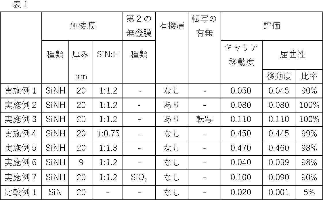
表1から本発明の有機薄膜トランジスタは、比較例に比べて、屈曲試験後のキャリア移動度の低下が小さく、屈曲性が高いことがわかる。
また、実施例1と実施例2との対比から、無機膜の下地層となる有機層を有するのが好ましいことがわかる。
また、実施例2と実施例3との対比から、無機膜を転写によって積層するのが好ましいことがわかる。
また、実施例1、実施例4、および実施例5の対比から、SiNとHとの原子数の比率SiN:Hは、1:0.9~1.5であるのがより好ましいことがわかる。
また、実施例1と実施例6との対比から無機膜の厚みは、10nm以上であるのが好ましいことがわかる。
また、実施例1と実施例7との対比から、第2の無機膜を有するのが好ましいことがわかる。
以上の結果より、本発明の効果は明らかである。 Table 1 shows that the organic thin film transistor of the present invention has a smaller decrease in carrier mobility after the bending test and a higher flexibility than the comparative example.
From the comparison between Example 1 and Example 2, it can be seen that it is preferable to have an organic layer serving as a base layer of the inorganic film.
Further, a comparison between Example 2 and Example 3 indicates that it is preferable to stack the inorganic films by transfer.
Also, from the comparison between Example 1, Example 4, and Example 5, it is understood that the ratio of the number of atoms between SiN and H, SiN: H, is more preferably 1: 0.9 to 1.5. .
Also, from the comparison between Example 1 and Example 6, it is understood that the thickness of the inorganic film is preferably 10 nm or more.
Further, from the comparison between Example 1 and Example 7, it can be seen that it is preferable to have the second inorganic film.
From the above results, the effect of the present invention is clear.
10、10a~10d 有機薄膜トランジスタ
12 支持体
18 トランジスタ素子
20 ゲート電極
21 有機層
22 SiNH膜(無機膜、絶縁膜)
23 第2の無機膜(SiO2膜)
24 有機半導体層
26 ソース電極
28 ドレイン電極
30 樹脂層
32 基板
40 転写型積層フィルム 10, 10a to 10d Organicthin film transistor 12 Support 18 Transistor element 20 Gate electrode 21 Organic layer 22 SiNH film (inorganic film, insulating film)
23 Second inorganic film (SiO 2 film)
Reference Signs List 24 organic semiconductor layer 26 source electrode 28 drain electrode 30 resin layer 32 substrate 40 transfer-type laminated film
12 支持体
18 トランジスタ素子
20 ゲート電極
21 有機層
22 SiNH膜(無機膜、絶縁膜)
23 第2の無機膜(SiO2膜)
24 有機半導体層
26 ソース電極
28 ドレイン電極
30 樹脂層
32 基板
40 転写型積層フィルム 10, 10a to 10d Organic
23 Second inorganic film (SiO 2 film)
Claims (10)
- ゲート電極と、
前記ゲート電極を覆って形成される絶縁膜と、
前記絶縁膜上に形成される有機半導体層と、
前記有機半導体層上に形成されるソース電極、および、ドレイン電極を有し、
前記絶縁膜は、SiNHからなる無機膜を含む有機薄膜トランジスタ。 A gate electrode;
An insulating film formed to cover the gate electrode;
An organic semiconductor layer formed on the insulating film,
Having a source electrode and a drain electrode formed on the organic semiconductor layer,
An organic thin film transistor, wherein the insulating film includes an inorganic film made of SiNH. - 前記無機膜中のSiNとHとの原子数の比率SiN:Hが、1:0.7~2である請求項1に記載の有機薄膜トランジスタ。 The organic thin film transistor according to claim 1, wherein the ratio SiN: H of the number of atoms between SiN and H in the inorganic film is 1: 0.7 to 2.
- 前記無機膜の厚みが1nm~100nmである請求項1または2に記載の有機薄膜トランジスタ。 (3) The organic thin film transistor according to (1) or (2), wherein the thickness of the inorganic film is 1 nm to 100 nm.
- 前記無機膜の前記ゲート電極側に有機層を有する請求項1~3のいずれか一項に記載の有機薄膜トランジスタ。 4. The organic thin-film transistor according to claim 1, further comprising an organic layer on the side of the gate electrode of the inorganic film.
- 前記有機層の厚みが0.01μm~1μmである請求項4に記載の有機薄膜トランジスタ。 The organic thin-film transistor according to claim 4, wherein the thickness of the organic layer is 0.01 μm to 1 μm.
- 前記有機層のガラス転移温度が200℃以上である請求項4または5に記載の有機薄膜トランジスタ。 The organic thin-film transistor according to claim 4 or 5, wherein the organic layer has a glass transition temperature of 200 ° C or higher.
- 前記無機膜の前記有機半導体層側の表面にSiO2をからなる第2の無機膜を有する請求項1~6のいずれか一項に記載の有機薄膜トランジスタ。 7. The organic thin-film transistor according to claim 1, further comprising a second inorganic film made of SiO 2 on a surface of the inorganic film on the side of the organic semiconductor layer.
- 前記ゲート電極、前記絶縁膜、前記有機半導体層、前記ソース電極、および、前記ドレイン電極を支持する支持体を有する請求項1~7のいずれか一項に記載の有機薄膜トランジスタ。 8. The organic thin-film transistor according to claim 1, further comprising a support for supporting the gate electrode, the insulating film, the organic semiconductor layer, the source electrode, and the drain electrode.
- 請求項1~8のいずれか一項に記載の有機薄膜トランジスタの製造方法であって、
支持体上にゲート電極を形成するゲート電極形成工程と、
前記ゲート電極の上に絶縁膜を積層する絶縁膜積層工程と、
前記絶縁膜の上に有機半導体層を形成する有機半導体層形成工程と
前記有機半導体層の上にソース電極およびドレイン電極を形成するソースドレイン電極形成工程とを有し、
前記絶縁膜は、SiNHからなる無機層を含む有機薄膜トランジスタの製造方法。 A method for producing an organic thin film transistor according to any one of claims 1 to 8,
A gate electrode forming step of forming a gate electrode on the support,
An insulating film laminating step of laminating an insulating film on the gate electrode,
An organic semiconductor layer forming step of forming an organic semiconductor layer on the insulating film, and a source / drain electrode forming step of forming a source electrode and a drain electrode on the organic semiconductor layer,
The method for manufacturing an organic thin film transistor, wherein the insulating film includes an inorganic layer made of SiNH. - 前記絶縁膜積層工程は、
基板と、基板上に形成された前記無機層を含む転写層とを有する転写型積層フィルムを前記ゲート電極の上に積層した後に、
前記転写層から前記基板を剥離することで、前記ゲート電極の上に前記絶縁膜を積層する請求項9に記載の有機薄膜トランジスタの製造方法。 The insulating film laminating step,
After laminating a transfer type laminated film having a substrate and a transfer layer including the inorganic layer formed on the substrate on the gate electrode,
The method according to claim 9, wherein the insulating film is stacked on the gate electrode by peeling the substrate from the transfer layer.
Priority Applications (3)
| Application Number | Priority Date | Filing Date | Title |
|---|---|---|---|
| EP19858491.4A EP3848977A4 (en) | 2018-09-03 | 2019-08-09 | Organic thin film transistor and method of manufacturing organic thin film transistor |
| JP2020541090A JP7083396B2 (en) | 2018-09-03 | 2019-08-09 | Organic thin film transistor and manufacturing method of organic thin film transistor |
| US17/186,275 US20210184142A1 (en) | 2018-09-03 | 2021-02-26 | Organic thin film transistor and method of manufacturing organic thin film transistor |
Applications Claiming Priority (2)
| Application Number | Priority Date | Filing Date | Title |
|---|---|---|---|
| JP2018-164317 | 2018-09-03 | ||
| JP2018164317 | 2018-09-03 |
Related Child Applications (1)
| Application Number | Title | Priority Date | Filing Date |
|---|---|---|---|
| US17/186,275 Continuation US20210184142A1 (en) | 2018-09-03 | 2021-02-26 | Organic thin film transistor and method of manufacturing organic thin film transistor |
Publications (1)
| Publication Number | Publication Date |
|---|---|
| WO2020049956A1 true WO2020049956A1 (en) | 2020-03-12 |
Family
ID=69722458
Family Applications (1)
| Application Number | Title | Priority Date | Filing Date |
|---|---|---|---|
| PCT/JP2019/031628 WO2020049956A1 (en) | 2018-09-03 | 2019-08-09 | Organic thin film transistor and method of manufacturing organic thin film transistor |
Country Status (4)
| Country | Link |
|---|---|
| US (1) | US20210184142A1 (en) |
| EP (1) | EP3848977A4 (en) |
| JP (1) | JP7083396B2 (en) |
| WO (1) | WO2020049956A1 (en) |
Citations (10)
| Publication number | Priority date | Publication date | Assignee | Title |
|---|---|---|---|---|
| JP2005311365A (en) * | 2004-04-20 | 2005-11-04 | Applied Materials Inc | Control of characteristics and uniformity of silicon nitride film by controlling film forming precursor |
| JP2006013480A (en) * | 2004-05-28 | 2006-01-12 | Semiconductor Energy Lab Co Ltd | Thin film transistor, display, methods of manufacturing them, and television device |
| JP2006093667A (en) * | 2004-08-23 | 2006-04-06 | Semiconductor Energy Lab Co Ltd | Method for manufacturing semiconductor devices |
| JP2007027525A (en) * | 2005-07-20 | 2007-02-01 | Sony Corp | Method of manufacturing semiconductor device, semiconductor device, and method of forming insulation film |
| JP2013084725A (en) * | 2011-10-07 | 2013-05-09 | Sumitomo Electric Ind Ltd | Semiconductor element |
| JP2015170760A (en) | 2014-03-07 | 2015-09-28 | 富士フイルム株式会社 | organic thin film transistor |
| JP2015177099A (en) | 2014-03-17 | 2015-10-05 | ソニー株式会社 | Transistor and display device |
| JP2015195361A (en) | 2014-03-26 | 2015-11-05 | 富士フイルム株式会社 | Provision of coating liquid for nonluminous organic semiconductor devices, organic transistor, compound, organic semiconductor material for nonluminous organic semiconductor devices, material for organic transistors, method for manufacturing organic transistor, and method for manufacturing organic semiconductor film |
| JP2017171736A (en) * | 2016-03-22 | 2017-09-28 | 日産化学工業株式会社 | Manufacturing method of heat conductive resin film |
| JP2018006745A (en) | 2016-06-27 | 2018-01-11 | 富士フイルム株式会社 | Organic thin film transistor, organic semiconductor film, compound, composition for organic thin film transistor, and method for manufacturing organic thin film transistor |
Family Cites Families (3)
| Publication number | Priority date | Publication date | Assignee | Title |
|---|---|---|---|---|
| JP5055844B2 (en) | 2006-06-05 | 2012-10-24 | コニカミノルタホールディングス株式会社 | Organic thin film transistor and method for producing organic thin film transistor |
| CN102683593B (en) * | 2012-03-29 | 2015-02-18 | 京东方科技集团股份有限公司 | Manufacturing method of organic thin-film transistor array substrate |
| JP2016058682A (en) * | 2014-09-12 | 2016-04-21 | 株式会社東芝 | Semiconductor device |
-
2019
- 2019-08-09 EP EP19858491.4A patent/EP3848977A4/en active Pending
- 2019-08-09 WO PCT/JP2019/031628 patent/WO2020049956A1/en unknown
- 2019-08-09 JP JP2020541090A patent/JP7083396B2/en active Active
-
2021
- 2021-02-26 US US17/186,275 patent/US20210184142A1/en not_active Abandoned
Patent Citations (10)
| Publication number | Priority date | Publication date | Assignee | Title |
|---|---|---|---|---|
| JP2005311365A (en) * | 2004-04-20 | 2005-11-04 | Applied Materials Inc | Control of characteristics and uniformity of silicon nitride film by controlling film forming precursor |
| JP2006013480A (en) * | 2004-05-28 | 2006-01-12 | Semiconductor Energy Lab Co Ltd | Thin film transistor, display, methods of manufacturing them, and television device |
| JP2006093667A (en) * | 2004-08-23 | 2006-04-06 | Semiconductor Energy Lab Co Ltd | Method for manufacturing semiconductor devices |
| JP2007027525A (en) * | 2005-07-20 | 2007-02-01 | Sony Corp | Method of manufacturing semiconductor device, semiconductor device, and method of forming insulation film |
| JP2013084725A (en) * | 2011-10-07 | 2013-05-09 | Sumitomo Electric Ind Ltd | Semiconductor element |
| JP2015170760A (en) | 2014-03-07 | 2015-09-28 | 富士フイルム株式会社 | organic thin film transistor |
| JP2015177099A (en) | 2014-03-17 | 2015-10-05 | ソニー株式会社 | Transistor and display device |
| JP2015195361A (en) | 2014-03-26 | 2015-11-05 | 富士フイルム株式会社 | Provision of coating liquid for nonluminous organic semiconductor devices, organic transistor, compound, organic semiconductor material for nonluminous organic semiconductor devices, material for organic transistors, method for manufacturing organic transistor, and method for manufacturing organic semiconductor film |
| JP2017171736A (en) * | 2016-03-22 | 2017-09-28 | 日産化学工業株式会社 | Manufacturing method of heat conductive resin film |
| JP2018006745A (en) | 2016-06-27 | 2018-01-11 | 富士フイルム株式会社 | Organic thin film transistor, organic semiconductor film, compound, composition for organic thin film transistor, and method for manufacturing organic thin film transistor |
Non-Patent Citations (1)
| Title |
|---|
| See also references of EP3848977A4 |
Also Published As
| Publication number | Publication date |
|---|---|
| US20210184142A1 (en) | 2021-06-17 |
| JPWO2020049956A1 (en) | 2021-08-12 |
| JP7083396B2 (en) | 2022-06-10 |
| EP3848977A1 (en) | 2021-07-14 |
| EP3848977A4 (en) | 2021-11-03 |
Similar Documents
| Publication | Publication Date | Title |
|---|---|---|
| US9282648B2 (en) | Composite electrode and method of manufacture thereof | |
| CN107405880B (en) | Film for laminating transparent conductive layer, method for producing same, and transparent conductive film | |
| JP5691175B2 (en) | Method for producing gas barrier film, gas barrier film, and organic photoelectric conversion element | |
| TWI686454B (en) | Adhesive sheet, two-sided adhesive sheet and optical element | |
| KR20130024965A (en) | Method for producing laminated film | |
| JPWO2020138206A1 (en) | Gas barrier laminate | |
| TWI757255B (en) | Transparent conductive layer lamination film, method for producing the same, and transparent conductive film | |
| WO2013081003A1 (en) | Manufacturing method for gas barrier film, and electronic member or optical member provided with gas barrier film | |
| WO2020049956A1 (en) | Organic thin film transistor and method of manufacturing organic thin film transistor | |
| JP6816916B2 (en) | Manufacturing method of transparent conductive laminate and transparent conductive laminate | |
| JP7112505B2 (en) | Electronic device laminate manufacturing method and electronic device laminate | |
| JP7158485B2 (en) | Organic thin film transistor and method for manufacturing organic thin film transistor | |
| JP6603811B2 (en) | Gas barrier film and method for producing gas barrier film | |
| JP6924893B2 (en) | Manufacturing method of gas barrier film, optical element and gas barrier film | |
| WO2018207508A1 (en) | Gas barrier film and method for producing gas barrier film | |
| JP2004058049A (en) | Film formation method | |
| JP6802842B2 (en) | Manufacturing method of transparent electrode | |
| WO2018180961A1 (en) | Transparent conductive laminate and production method therefor | |
| JP2008238660A (en) | Planar substrate |
Legal Events
| Date | Code | Title | Description |
|---|---|---|---|
| 121 | Ep: the epo has been informed by wipo that ep was designated in this application |
Ref document number: 19858491 Country of ref document: EP Kind code of ref document: A1 |
|
| ENP | Entry into the national phase |
Ref document number: 2020541090 Country of ref document: JP Kind code of ref document: A |
|
| NENP | Non-entry into the national phase |
Ref country code: DE |
|
| ENP | Entry into the national phase |
Ref document number: 2019858491 Country of ref document: EP Effective date: 20210406 |