WO2020049397A1 - 表示装置、表示モジュール、及び電子機器 - Google Patents
表示装置、表示モジュール、及び電子機器 Download PDFInfo
- Publication number
- WO2020049397A1 WO2020049397A1 PCT/IB2019/057136 IB2019057136W WO2020049397A1 WO 2020049397 A1 WO2020049397 A1 WO 2020049397A1 IB 2019057136 W IB2019057136 W IB 2019057136W WO 2020049397 A1 WO2020049397 A1 WO 2020049397A1
- Authority
- WO
- WIPO (PCT)
- Prior art keywords
- conductive layer
- emitting diode
- light emitting
- electrode
- transistor
- Prior art date
Links
- 229910044991 metal oxide Inorganic materials 0.000 claims description 66
- 150000004706 metal oxides Chemical class 0.000 claims description 56
- 230000015572 biosynthetic process Effects 0.000 claims description 14
- 239000003086 colorant Substances 0.000 claims description 5
- 239000010410 layer Substances 0.000 description 447
- 230000006870 function Effects 0.000 description 78
- 239000000758 substrate Substances 0.000 description 77
- 239000004065 semiconductor Substances 0.000 description 69
- 238000000034 method Methods 0.000 description 26
- 239000000463 material Substances 0.000 description 24
- 239000013078 crystal Substances 0.000 description 20
- 238000006243 chemical reaction Methods 0.000 description 19
- 230000003287 optical effect Effects 0.000 description 18
- 239000004020 conductor Substances 0.000 description 17
- 229910052738 indium Inorganic materials 0.000 description 16
- APFVFJFRJDLVQX-UHFFFAOYSA-N indium atom Chemical compound [In] APFVFJFRJDLVQX-UHFFFAOYSA-N 0.000 description 16
- 239000002096 quantum dot Substances 0.000 description 16
- 239000010949 copper Substances 0.000 description 15
- 229920005989 resin Polymers 0.000 description 15
- 239000011347 resin Substances 0.000 description 15
- RYGMFSIKBFXOCR-UHFFFAOYSA-N Copper Chemical compound [Cu] RYGMFSIKBFXOCR-UHFFFAOYSA-N 0.000 description 14
- 229910052802 copper Inorganic materials 0.000 description 14
- 229910052782 aluminium Inorganic materials 0.000 description 13
- XAGFODPZIPBFFR-UHFFFAOYSA-N aluminium Chemical compound [Al] XAGFODPZIPBFFR-UHFFFAOYSA-N 0.000 description 13
- QVGXLLKOCUKJST-UHFFFAOYSA-N atomic oxygen Chemical compound [O] QVGXLLKOCUKJST-UHFFFAOYSA-N 0.000 description 13
- 229910052760 oxygen Inorganic materials 0.000 description 13
- 239000001301 oxygen Substances 0.000 description 13
- 150000001875 compounds Chemical class 0.000 description 12
- 239000011701 zinc Substances 0.000 description 12
- XUIMIQQOPSSXEZ-UHFFFAOYSA-N Silicon Chemical compound [Si] XUIMIQQOPSSXEZ-UHFFFAOYSA-N 0.000 description 11
- 239000012790 adhesive layer Substances 0.000 description 11
- 229910052710 silicon Inorganic materials 0.000 description 11
- 239000010703 silicon Substances 0.000 description 11
- 229910052719 titanium Inorganic materials 0.000 description 11
- 239000010936 titanium Substances 0.000 description 11
- RTAQQCXQSZGOHL-UHFFFAOYSA-N Titanium Chemical compound [Ti] RTAQQCXQSZGOHL-UHFFFAOYSA-N 0.000 description 10
- GYHNNYVSQQEPJS-UHFFFAOYSA-N Gallium Chemical compound [Ga] GYHNNYVSQQEPJS-UHFFFAOYSA-N 0.000 description 9
- 229910052733 gallium Inorganic materials 0.000 description 9
- 238000004519 manufacturing process Methods 0.000 description 9
- 238000007789 sealing Methods 0.000 description 9
- PXHVJJICTQNCMI-UHFFFAOYSA-N Nickel Chemical compound [Ni] PXHVJJICTQNCMI-UHFFFAOYSA-N 0.000 description 8
- 229910052751 metal Inorganic materials 0.000 description 8
- 239000011241 protective layer Substances 0.000 description 8
- BUGBHKTXTAQXES-UHFFFAOYSA-N Selenium Chemical compound [Se] BUGBHKTXTAQXES-UHFFFAOYSA-N 0.000 description 7
- HCHKCACWOHOZIP-UHFFFAOYSA-N Zinc Chemical compound [Zn] HCHKCACWOHOZIP-UHFFFAOYSA-N 0.000 description 7
- 238000004040 coloring Methods 0.000 description 7
- 238000004891 communication Methods 0.000 description 7
- 239000012535 impurity Substances 0.000 description 7
- 229910052711 selenium Inorganic materials 0.000 description 7
- 239000011669 selenium Substances 0.000 description 7
- 229910052725 zinc Inorganic materials 0.000 description 7
- IJGRMHOSHXDMSA-UHFFFAOYSA-N Atomic nitrogen Chemical compound N#N IJGRMHOSHXDMSA-UHFFFAOYSA-N 0.000 description 6
- UFHFLCQGNIYNRP-UHFFFAOYSA-N Hydrogen Chemical compound [H][H] UFHFLCQGNIYNRP-UHFFFAOYSA-N 0.000 description 6
- VYPSYNLAJGMNEJ-UHFFFAOYSA-N Silicium dioxide Chemical compound O=[Si]=O VYPSYNLAJGMNEJ-UHFFFAOYSA-N 0.000 description 6
- -1 copper-magnesium-aluminum Chemical compound 0.000 description 6
- 229910052739 hydrogen Inorganic materials 0.000 description 6
- 239000001257 hydrogen Substances 0.000 description 6
- 239000011159 matrix material Substances 0.000 description 6
- 239000002184 metal Substances 0.000 description 6
- 239000002159 nanocrystal Substances 0.000 description 6
- 229910052721 tungsten Inorganic materials 0.000 description 6
- ZOKXTWBITQBERF-UHFFFAOYSA-N Molybdenum Chemical compound [Mo] ZOKXTWBITQBERF-UHFFFAOYSA-N 0.000 description 5
- OAICVXFJPJFONN-UHFFFAOYSA-N Phosphorus Chemical compound [P] OAICVXFJPJFONN-UHFFFAOYSA-N 0.000 description 5
- 229910052581 Si3N4 Inorganic materials 0.000 description 5
- BQCADISMDOOEFD-UHFFFAOYSA-N Silver Chemical compound [Ag] BQCADISMDOOEFD-UHFFFAOYSA-N 0.000 description 5
- XLOMVQKBTHCTTD-UHFFFAOYSA-N Zinc monoxide Chemical compound [Zn]=O XLOMVQKBTHCTTD-UHFFFAOYSA-N 0.000 description 5
- 239000000956 alloy Substances 0.000 description 5
- 239000003990 capacitor Substances 0.000 description 5
- 239000011521 glass Substances 0.000 description 5
- 229910052750 molybdenum Inorganic materials 0.000 description 5
- 239000011733 molybdenum Substances 0.000 description 5
- HQVNEWCFYHHQES-UHFFFAOYSA-N silicon nitride Chemical compound N12[Si]34N5[Si]62N3[Si]51N64 HQVNEWCFYHHQES-UHFFFAOYSA-N 0.000 description 5
- 229910052709 silver Inorganic materials 0.000 description 5
- 239000004332 silver Substances 0.000 description 5
- WFKWXMTUELFFGS-UHFFFAOYSA-N tungsten Chemical compound [W] WFKWXMTUELFFGS-UHFFFAOYSA-N 0.000 description 5
- 239000010937 tungsten Substances 0.000 description 5
- XEEYBQQBJWHFJM-UHFFFAOYSA-N Iron Chemical compound [Fe] XEEYBQQBJWHFJM-UHFFFAOYSA-N 0.000 description 4
- 229910045601 alloy Inorganic materials 0.000 description 4
- 230000004888 barrier function Effects 0.000 description 4
- 229910052796 boron Inorganic materials 0.000 description 4
- 229910052800 carbon group element Inorganic materials 0.000 description 4
- 239000000919 ceramic Substances 0.000 description 4
- PCHJSUWPFVWCPO-UHFFFAOYSA-N gold Chemical compound [Au] PCHJSUWPFVWCPO-UHFFFAOYSA-N 0.000 description 4
- 229910052737 gold Inorganic materials 0.000 description 4
- 239000010931 gold Substances 0.000 description 4
- 230000007246 mechanism Effects 0.000 description 4
- 229910052759 nickel Inorganic materials 0.000 description 4
- TWNQGVIAIRXVLR-UHFFFAOYSA-N oxo(oxoalumanyloxy)alumane Chemical compound O=[Al]O[Al]=O TWNQGVIAIRXVLR-UHFFFAOYSA-N 0.000 description 4
- HBMJWWWQQXIZIP-UHFFFAOYSA-N silicon carbide Chemical compound [Si+]#[C-] HBMJWWWQQXIZIP-UHFFFAOYSA-N 0.000 description 4
- 229910052814 silicon oxide Inorganic materials 0.000 description 4
- 229910052727 yttrium Inorganic materials 0.000 description 4
- 229910002601 GaN Inorganic materials 0.000 description 3
- JMASRVWKEDWRBT-UHFFFAOYSA-N Gallium nitride Chemical compound [Ga]#N JMASRVWKEDWRBT-UHFFFAOYSA-N 0.000 description 3
- KDLHZDBZIXYQEI-UHFFFAOYSA-N Palladium Chemical compound [Pd] KDLHZDBZIXYQEI-UHFFFAOYSA-N 0.000 description 3
- 239000004642 Polyimide Substances 0.000 description 3
- ATJFFYVFTNAWJD-UHFFFAOYSA-N Tin Chemical compound [Sn] ATJFFYVFTNAWJD-UHFFFAOYSA-N 0.000 description 3
- QCWXUUIWCKQGHC-UHFFFAOYSA-N Zirconium Chemical compound [Zr] QCWXUUIWCKQGHC-UHFFFAOYSA-N 0.000 description 3
- 230000001133 acceleration Effects 0.000 description 3
- NIXOWILDQLNWCW-UHFFFAOYSA-N acrylic acid group Chemical group C(C=C)(=O)O NIXOWILDQLNWCW-UHFFFAOYSA-N 0.000 description 3
- 229910052785 arsenic Inorganic materials 0.000 description 3
- 150000001495 arsenic compounds Chemical class 0.000 description 3
- 229910052798 chalcogen Inorganic materials 0.000 description 3
- 238000001514 detection method Methods 0.000 description 3
- 230000000694 effects Effects 0.000 description 3
- 230000005669 field effect Effects 0.000 description 3
- 229910052732 germanium Inorganic materials 0.000 description 3
- GNPVGFCGXDBREM-UHFFFAOYSA-N germanium atom Chemical compound [Ge] GNPVGFCGXDBREM-UHFFFAOYSA-N 0.000 description 3
- UQSXHKLRYXJYBZ-UHFFFAOYSA-N iron oxide Inorganic materials [Fe]=O UQSXHKLRYXJYBZ-UHFFFAOYSA-N 0.000 description 3
- 229910021421 monocrystalline silicon Inorganic materials 0.000 description 3
- 229910052757 nitrogen Inorganic materials 0.000 description 3
- 229910052698 phosphorus Inorganic materials 0.000 description 3
- 239000011574 phosphorus Substances 0.000 description 3
- 229910052696 pnictogen Inorganic materials 0.000 description 3
- 229920001721 polyimide Polymers 0.000 description 3
- 230000001681 protective effect Effects 0.000 description 3
- 229910010271 silicon carbide Inorganic materials 0.000 description 3
- 239000000126 substance Substances 0.000 description 3
- 229910052715 tantalum Inorganic materials 0.000 description 3
- GUVRBAGPIYLISA-UHFFFAOYSA-N tantalum atom Chemical compound [Ta] GUVRBAGPIYLISA-UHFFFAOYSA-N 0.000 description 3
- 229910052718 tin Inorganic materials 0.000 description 3
- XLYOFNOQVPJJNP-UHFFFAOYSA-N water Substances O XLYOFNOQVPJJNP-UHFFFAOYSA-N 0.000 description 3
- VWQVUPCCIRVNHF-UHFFFAOYSA-N yttrium atom Chemical compound [Y] VWQVUPCCIRVNHF-UHFFFAOYSA-N 0.000 description 3
- 239000011787 zinc oxide Substances 0.000 description 3
- 229910052726 zirconium Inorganic materials 0.000 description 3
- ZOXJGFHDIHLPTG-UHFFFAOYSA-N Boron Chemical compound [B] ZOXJGFHDIHLPTG-UHFFFAOYSA-N 0.000 description 2
- OKTJSMMVPCPJKN-UHFFFAOYSA-N Carbon Chemical compound [C] OKTJSMMVPCPJKN-UHFFFAOYSA-N 0.000 description 2
- 229910052684 Cerium Inorganic materials 0.000 description 2
- 239000004593 Epoxy Substances 0.000 description 2
- FYYHWMGAXLPEAU-UHFFFAOYSA-N Magnesium Chemical compound [Mg] FYYHWMGAXLPEAU-UHFFFAOYSA-N 0.000 description 2
- 229910052779 Neodymium Inorganic materials 0.000 description 2
- 229910000577 Silicon-germanium Inorganic materials 0.000 description 2
- NINIDFKCEFEMDL-UHFFFAOYSA-N Sulfur Chemical compound [S] NINIDFKCEFEMDL-UHFFFAOYSA-N 0.000 description 2
- NRTOMJZYCJJWKI-UHFFFAOYSA-N Titanium nitride Chemical compound [Ti]#N NRTOMJZYCJJWKI-UHFFFAOYSA-N 0.000 description 2
- LEVVHYCKPQWKOP-UHFFFAOYSA-N [Si].[Ge] Chemical compound [Si].[Ge] LEVVHYCKPQWKOP-UHFFFAOYSA-N 0.000 description 2
- RQNWIZPPADIBDY-UHFFFAOYSA-N arsenic atom Chemical compound [As] RQNWIZPPADIBDY-UHFFFAOYSA-N 0.000 description 2
- 125000004429 atom Chemical group 0.000 description 2
- GPBUGPUPKAGMDK-UHFFFAOYSA-N azanylidynemolybdenum Chemical compound [Mo]#N GPBUGPUPKAGMDK-UHFFFAOYSA-N 0.000 description 2
- 229910052795 boron group element Inorganic materials 0.000 description 2
- 229910052793 cadmium Inorganic materials 0.000 description 2
- BDOSMKKIYDKNTQ-UHFFFAOYSA-N cadmium atom Chemical compound [Cd] BDOSMKKIYDKNTQ-UHFFFAOYSA-N 0.000 description 2
- 229910052799 carbon Inorganic materials 0.000 description 2
- 239000000969 carrier Substances 0.000 description 2
- ZMIGMASIKSOYAM-UHFFFAOYSA-N cerium Chemical compound [Ce][Ce][Ce][Ce][Ce][Ce][Ce][Ce][Ce][Ce][Ce][Ce][Ce][Ce][Ce][Ce][Ce][Ce][Ce][Ce][Ce][Ce][Ce][Ce][Ce][Ce][Ce][Ce][Ce][Ce][Ce][Ce][Ce][Ce][Ce][Ce][Ce][Ce] ZMIGMASIKSOYAM-UHFFFAOYSA-N 0.000 description 2
- PMHQVHHXPFUNSP-UHFFFAOYSA-M copper(1+);methylsulfanylmethane;bromide Chemical compound Br[Cu].CSC PMHQVHHXPFUNSP-UHFFFAOYSA-M 0.000 description 2
- 230000007547 defect Effects 0.000 description 2
- 238000010586 diagram Methods 0.000 description 2
- 238000009792 diffusion process Methods 0.000 description 2
- 238000006073 displacement reaction Methods 0.000 description 2
- 230000005684 electric field Effects 0.000 description 2
- 238000000295 emission spectrum Methods 0.000 description 2
- 239000003822 epoxy resin Substances 0.000 description 2
- 229910052735 hafnium Inorganic materials 0.000 description 2
- VBJZVLUMGGDVMO-UHFFFAOYSA-N hafnium atom Chemical compound [Hf] VBJZVLUMGGDVMO-UHFFFAOYSA-N 0.000 description 2
- 229910000449 hafnium oxide Inorganic materials 0.000 description 2
- WIHZLLGSGQNAGK-UHFFFAOYSA-N hafnium(4+);oxygen(2-) Chemical compound [O-2].[O-2].[Hf+4] WIHZLLGSGQNAGK-UHFFFAOYSA-N 0.000 description 2
- 229910052736 halogen Inorganic materials 0.000 description 2
- 210000003128 head Anatomy 0.000 description 2
- AMWRITDGCCNYAT-UHFFFAOYSA-L hydroxy(oxo)manganese;manganese Chemical compound [Mn].O[Mn]=O.O[Mn]=O AMWRITDGCCNYAT-UHFFFAOYSA-L 0.000 description 2
- 238000007654 immersion Methods 0.000 description 2
- 229910052742 iron Inorganic materials 0.000 description 2
- 235000013980 iron oxide Nutrition 0.000 description 2
- 238000002955 isolation Methods 0.000 description 2
- 229910052746 lanthanum Inorganic materials 0.000 description 2
- FZLIPJUXYLNCLC-UHFFFAOYSA-N lanthanum atom Chemical compound [La] FZLIPJUXYLNCLC-UHFFFAOYSA-N 0.000 description 2
- 239000010985 leather Substances 0.000 description 2
- 239000007788 liquid Substances 0.000 description 2
- 229910052749 magnesium Inorganic materials 0.000 description 2
- 239000011777 magnesium Substances 0.000 description 2
- 230000005389 magnetism Effects 0.000 description 2
- QEFYFXOXNSNQGX-UHFFFAOYSA-N neodymium atom Chemical compound [Nd] QEFYFXOXNSNQGX-UHFFFAOYSA-N 0.000 description 2
- 230000001151 other effect Effects 0.000 description 2
- BASFCYQUMIYNBI-UHFFFAOYSA-N platinum Chemical compound [Pt] BASFCYQUMIYNBI-UHFFFAOYSA-N 0.000 description 2
- 229910021420 polycrystalline silicon Inorganic materials 0.000 description 2
- 229920000647 polyepoxide Polymers 0.000 description 2
- 229920001296 polysiloxane Polymers 0.000 description 2
- 230000008569 process Effects 0.000 description 2
- 238000012545 processing Methods 0.000 description 2
- 125000006239 protecting group Chemical group 0.000 description 2
- 239000003223 protective agent Substances 0.000 description 2
- 239000010453 quartz Substances 0.000 description 2
- 230000005855 radiation Effects 0.000 description 2
- 230000009257 reactivity Effects 0.000 description 2
- 229910052594 sapphire Inorganic materials 0.000 description 2
- 239000010980 sapphire Substances 0.000 description 2
- UKGBSHWRVFPDKV-UHFFFAOYSA-N selanylideneberyllium Chemical compound [Se]=[Be] UKGBSHWRVFPDKV-UHFFFAOYSA-N 0.000 description 2
- 239000002356 single layer Substances 0.000 description 2
- 238000003860 storage Methods 0.000 description 2
- 229910052717 sulfur Inorganic materials 0.000 description 2
- 239000011593 sulfur Substances 0.000 description 2
- XSOKHXFFCGXDJZ-UHFFFAOYSA-N telluride(2-) Chemical compound [Te-2] XSOKHXFFCGXDJZ-UHFFFAOYSA-N 0.000 description 2
- OGIDPMRJRNCKJF-UHFFFAOYSA-N titanium oxide Inorganic materials [Ti]=O OGIDPMRJRNCKJF-UHFFFAOYSA-N 0.000 description 2
- SKJCKYVIQGBWTN-UHFFFAOYSA-N (4-hydroxyphenyl) methanesulfonate Chemical compound CS(=O)(=O)OC1=CC=C(O)C=C1 SKJCKYVIQGBWTN-UHFFFAOYSA-N 0.000 description 1
- PFNQVRZLDWYSCW-UHFFFAOYSA-N (fluoren-9-ylideneamino) n-naphthalen-1-ylcarbamate Chemical compound C12=CC=CC=C2C2=CC=CC=C2C1=NOC(=O)NC1=CC=CC2=CC=CC=C12 PFNQVRZLDWYSCW-UHFFFAOYSA-N 0.000 description 1
- IHGSAQHSAGRWNI-UHFFFAOYSA-N 1-(4-bromophenyl)-2,2,2-trifluoroethanone Chemical compound FC(F)(F)C(=O)C1=CC=C(Br)C=C1 IHGSAQHSAGRWNI-UHFFFAOYSA-N 0.000 description 1
- WUPHOULIZUERAE-UHFFFAOYSA-N 3-(oxolan-2-yl)propanoic acid Chemical compound OC(=O)CCC1CCCO1 WUPHOULIZUERAE-UHFFFAOYSA-N 0.000 description 1
- QIHHYQWNYKOHEV-UHFFFAOYSA-N 4-tert-butyl-3-nitrobenzoic acid Chemical compound CC(C)(C)C1=CC=C(C(O)=O)C=C1[N+]([O-])=O QIHHYQWNYKOHEV-UHFFFAOYSA-N 0.000 description 1
- MARUHZGHZWCEQU-UHFFFAOYSA-N 5-phenyl-2h-tetrazole Chemical compound C1=CC=CC=C1C1=NNN=N1 MARUHZGHZWCEQU-UHFFFAOYSA-N 0.000 description 1
- 229910001316 Ag alloy Inorganic materials 0.000 description 1
- 229910000838 Al alloy Inorganic materials 0.000 description 1
- JBRZTFJDHDCESZ-UHFFFAOYSA-N AsGa Chemical compound [As]#[Ga] JBRZTFJDHDCESZ-UHFFFAOYSA-N 0.000 description 1
- 229910052582 BN Inorganic materials 0.000 description 1
- PZNSFCLAULLKQX-UHFFFAOYSA-N Boron nitride Chemical compound N#B PZNSFCLAULLKQX-UHFFFAOYSA-N 0.000 description 1
- VYZAMTAEIAYCRO-UHFFFAOYSA-N Chromium Chemical compound [Cr] VYZAMTAEIAYCRO-UHFFFAOYSA-N 0.000 description 1
- QPLDLSVMHZLSFG-UHFFFAOYSA-N Copper oxide Chemical compound [Cu]=O QPLDLSVMHZLSFG-UHFFFAOYSA-N 0.000 description 1
- 239000005751 Copper oxide Substances 0.000 description 1
- 229910021594 Copper(II) fluoride Inorganic materials 0.000 description 1
- MYMOFIZGZYHOMD-UHFFFAOYSA-N Dioxygen Chemical compound O=O MYMOFIZGZYHOMD-UHFFFAOYSA-N 0.000 description 1
- JOYRKODLDBILNP-UHFFFAOYSA-N Ethyl urethane Chemical compound CCOC(N)=O JOYRKODLDBILNP-UHFFFAOYSA-N 0.000 description 1
- MBMLMWLHJBBADN-UHFFFAOYSA-N Ferrous sulfide Chemical compound [Fe]=S MBMLMWLHJBBADN-UHFFFAOYSA-N 0.000 description 1
- 229910005540 GaP Inorganic materials 0.000 description 1
- 229910001218 Gallium arsenide Inorganic materials 0.000 description 1
- 206010021143 Hypoxia Diseases 0.000 description 1
- 229910000673 Indium arsenide Inorganic materials 0.000 description 1
- GPXJNWSHGFTCBW-UHFFFAOYSA-N Indium phosphide Chemical compound [In]#P GPXJNWSHGFTCBW-UHFFFAOYSA-N 0.000 description 1
- 229910002668 Pd-Cu Inorganic materials 0.000 description 1
- UCKMPCXJQFINFW-UHFFFAOYSA-N Sulphide Chemical compound [S-2] UCKMPCXJQFINFW-UHFFFAOYSA-N 0.000 description 1
- GWEVSGVZZGPLCZ-UHFFFAOYSA-N Titan oxide Chemical compound O=[Ti]=O GWEVSGVZZGPLCZ-UHFFFAOYSA-N 0.000 description 1
- 239000005083 Zinc sulfide Substances 0.000 description 1
- DBKNIEBLJMAJHX-UHFFFAOYSA-N [As]#B Chemical compound [As]#B DBKNIEBLJMAJHX-UHFFFAOYSA-N 0.000 description 1
- XHCLAFWTIXFWPH-UHFFFAOYSA-N [O-2].[O-2].[O-2].[O-2].[O-2].[V+5].[V+5] Chemical compound [O-2].[O-2].[O-2].[O-2].[O-2].[V+5].[V+5] XHCLAFWTIXFWPH-UHFFFAOYSA-N 0.000 description 1
- 239000000853 adhesive Substances 0.000 description 1
- 230000001070 adhesive effect Effects 0.000 description 1
- 230000002776 aggregation Effects 0.000 description 1
- 238000004220 aggregation Methods 0.000 description 1
- LVQULNGDVIKLPK-UHFFFAOYSA-N aluminium antimonide Chemical compound [Sb]#[Al] LVQULNGDVIKLPK-UHFFFAOYSA-N 0.000 description 1
- MDPILPRLPQYEEN-UHFFFAOYSA-N aluminium arsenide Chemical compound [As]#[Al] MDPILPRLPQYEEN-UHFFFAOYSA-N 0.000 description 1
- PNEYBMLMFCGWSK-UHFFFAOYSA-N aluminium oxide Inorganic materials [O-2].[O-2].[O-2].[Al+3].[Al+3] PNEYBMLMFCGWSK-UHFFFAOYSA-N 0.000 description 1
- COOGPNLGKIHLSK-UHFFFAOYSA-N aluminium sulfide Chemical compound [Al+3].[Al+3].[S-2].[S-2].[S-2] COOGPNLGKIHLSK-UHFFFAOYSA-N 0.000 description 1
- 229910021417 amorphous silicon Inorganic materials 0.000 description 1
- 238000004458 analytical method Methods 0.000 description 1
- MRPWWVMHWSDJEH-UHFFFAOYSA-N antimony telluride Chemical compound [SbH3+3].[SbH3+3].[TeH2-2].[TeH2-2].[TeH2-2] MRPWWVMHWSDJEH-UHFFFAOYSA-N 0.000 description 1
- 230000003190 augmentative effect Effects 0.000 description 1
- NWAIGJYBQQYSPW-UHFFFAOYSA-N azanylidyneindigane Chemical compound [In]#N NWAIGJYBQQYSPW-UHFFFAOYSA-N 0.000 description 1
- CJDPJFRMHVXWPT-UHFFFAOYSA-N barium sulfide Chemical compound [S-2].[Ba+2] CJDPJFRMHVXWPT-UHFFFAOYSA-N 0.000 description 1
- RJWLRCHYHHXJLX-UHFFFAOYSA-N barium(2+);selenium(2-) Chemical compound [Se-2].[Ba+2] RJWLRCHYHHXJLX-UHFFFAOYSA-N 0.000 description 1
- QWTSUIVNFZQZJV-UHFFFAOYSA-H barium(2+);titanium(4+);diphosphate Chemical compound [Ti+4].[Ba+2].[O-]P([O-])([O-])=O.[O-]P([O-])([O-])=O QWTSUIVNFZQZJV-UHFFFAOYSA-H 0.000 description 1
- 230000005540 biological transmission Effects 0.000 description 1
- 229910052797 bismuth Inorganic materials 0.000 description 1
- JCXGWMGPZLAOME-UHFFFAOYSA-N bismuth atom Chemical compound [Bi] JCXGWMGPZLAOME-UHFFFAOYSA-N 0.000 description 1
- 230000000903 blocking effect Effects 0.000 description 1
- FFBGYFUYJVKRNV-UHFFFAOYSA-N boranylidynephosphane Chemical compound P#B FFBGYFUYJVKRNV-UHFFFAOYSA-N 0.000 description 1
- 210000000481 breast Anatomy 0.000 description 1
- ODWXUNBKCRECNW-UHFFFAOYSA-M bromocopper(1+) Chemical compound Br[Cu+] ODWXUNBKCRECNW-UHFFFAOYSA-M 0.000 description 1
- 229940065285 cadmium compound Drugs 0.000 description 1
- 150000001662 cadmium compounds Chemical class 0.000 description 1
- 229910052980 cadmium sulfide Inorganic materials 0.000 description 1
- UHYPYGJEEGLRJD-UHFFFAOYSA-N cadmium(2+);selenium(2-) Chemical compound [Se-2].[Cd+2] UHYPYGJEEGLRJD-UHFFFAOYSA-N 0.000 description 1
- JGIATAMCQXIDNZ-UHFFFAOYSA-N calcium sulfide Chemical compound [Ca]=S JGIATAMCQXIDNZ-UHFFFAOYSA-N 0.000 description 1
- NNLOHLDVJGPUFR-UHFFFAOYSA-L calcium;3,4,5,6-tetrahydroxy-2-oxohexanoate Chemical compound [Ca+2].OCC(O)C(O)C(O)C(=O)C([O-])=O.OCC(O)C(O)C(O)C(=O)C([O-])=O NNLOHLDVJGPUFR-UHFFFAOYSA-L 0.000 description 1
- QDVBBRPDXBHZFM-UHFFFAOYSA-N calcium;selenium(2-) Chemical compound [Ca+2].[Se-2] QDVBBRPDXBHZFM-UHFFFAOYSA-N 0.000 description 1
- 238000004364 calculation method Methods 0.000 description 1
- 150000004770 chalcogenides Chemical class 0.000 description 1
- 229910052804 chromium Inorganic materials 0.000 description 1
- 239000011651 chromium Substances 0.000 description 1
- 238000004140 cleaning Methods 0.000 description 1
- 238000000576 coating method Methods 0.000 description 1
- 229910000428 cobalt oxide Inorganic materials 0.000 description 1
- INPLXZPZQSLHBR-UHFFFAOYSA-N cobalt(2+);sulfide Chemical compound [S-2].[Co+2] INPLXZPZQSLHBR-UHFFFAOYSA-N 0.000 description 1
- IVMYJDGYRUAWML-UHFFFAOYSA-N cobalt(ii) oxide Chemical compound [Co]=O IVMYJDGYRUAWML-UHFFFAOYSA-N 0.000 description 1
- 239000002131 composite material Substances 0.000 description 1
- 238000011109 contamination Methods 0.000 description 1
- 229910000431 copper oxide Inorganic materials 0.000 description 1
- ORTQZVOHEJQUHG-UHFFFAOYSA-L copper(II) chloride Chemical compound Cl[Cu]Cl ORTQZVOHEJQUHG-UHFFFAOYSA-L 0.000 description 1
- GWFAVIIMQDUCRA-UHFFFAOYSA-L copper(ii) fluoride Chemical compound [F-].[F-].[Cu+2] GWFAVIIMQDUCRA-UHFFFAOYSA-L 0.000 description 1
- GBRBMTNGQBKBQE-UHFFFAOYSA-L copper;diiodide Chemical compound I[Cu]I GBRBMTNGQBKBQE-UHFFFAOYSA-L 0.000 description 1
- 239000011258 core-shell material Substances 0.000 description 1
- 229910021419 crystalline silicon Inorganic materials 0.000 description 1
- 230000007423 decrease Effects 0.000 description 1
- 238000013461 design Methods 0.000 description 1
- ZZEMEJKDTZOXOI-UHFFFAOYSA-N digallium;selenium(2-) Chemical compound [Ga+3].[Ga+3].[Se-2].[Se-2].[Se-2] ZZEMEJKDTZOXOI-UHFFFAOYSA-N 0.000 description 1
- 229910001882 dioxygen Inorganic materials 0.000 description 1
- 238000009826 distribution Methods 0.000 description 1
- 229920001971 elastomer Polymers 0.000 description 1
- 238000005530 etching Methods 0.000 description 1
- 230000001747 exhibiting effect Effects 0.000 description 1
- 239000004744 fabric Substances 0.000 description 1
- 210000001061 forehead Anatomy 0.000 description 1
- VTGARNNDLOTBET-UHFFFAOYSA-N gallium antimonide Chemical compound [Sb]#[Ga] VTGARNNDLOTBET-UHFFFAOYSA-N 0.000 description 1
- HZXMRANICFIONG-UHFFFAOYSA-N gallium phosphide Chemical compound [Ga]#P HZXMRANICFIONG-UHFFFAOYSA-N 0.000 description 1
- BIXHRBFZLLFBFL-UHFFFAOYSA-N germanium nitride Chemical compound N#[Ge]N([Ge]#N)[Ge]#N BIXHRBFZLLFBFL-UHFFFAOYSA-N 0.000 description 1
- GPMBECJIPQBCKI-UHFFFAOYSA-N germanium telluride Chemical compound [Te]=[Ge]=[Te] GPMBECJIPQBCKI-UHFFFAOYSA-N 0.000 description 1
- 230000017525 heat dissipation Effects 0.000 description 1
- 125000005842 heteroatom Chemical group 0.000 description 1
- WPYVAWXEWQSOGY-UHFFFAOYSA-N indium antimonide Chemical compound [Sb]#[In] WPYVAWXEWQSOGY-UHFFFAOYSA-N 0.000 description 1
- RPQDHPTXJYYUPQ-UHFFFAOYSA-N indium arsenide Chemical compound [In]#[As] RPQDHPTXJYYUPQ-UHFFFAOYSA-N 0.000 description 1
- 229910003437 indium oxide Inorganic materials 0.000 description 1
- AKUCEXGLFUSJCD-UHFFFAOYSA-N indium(3+);selenium(2-) Chemical compound [Se-2].[Se-2].[Se-2].[In+3].[In+3] AKUCEXGLFUSJCD-UHFFFAOYSA-N 0.000 description 1
- PJXISJQVUVHSOJ-UHFFFAOYSA-N indium(iii) oxide Chemical compound [O-2].[O-2].[O-2].[In+3].[In+3] PJXISJQVUVHSOJ-UHFFFAOYSA-N 0.000 description 1
- 239000011261 inert gas Substances 0.000 description 1
- 229910010272 inorganic material Inorganic materials 0.000 description 1
- 239000011147 inorganic material Substances 0.000 description 1
- 239000011810 insulating material Substances 0.000 description 1
- VBMVTYDPPZVILR-UHFFFAOYSA-N iron(2+);oxygen(2-) Chemical class [O-2].[Fe+2] VBMVTYDPPZVILR-UHFFFAOYSA-N 0.000 description 1
- 229910000464 lead oxide Inorganic materials 0.000 description 1
- 229910052981 lead sulfide Inorganic materials 0.000 description 1
- 229940056932 lead sulfide Drugs 0.000 description 1
- 239000002649 leather substitute Substances 0.000 description 1
- QENHCSSJTJWZAL-UHFFFAOYSA-N magnesium sulfide Chemical compound [Mg+2].[S-2] QENHCSSJTJWZAL-UHFFFAOYSA-N 0.000 description 1
- AZUPEYZKABXNLR-UHFFFAOYSA-N magnesium;selenium(2-) Chemical compound [Mg+2].[Se-2] AZUPEYZKABXNLR-UHFFFAOYSA-N 0.000 description 1
- WPBNNNQJVZRUHP-UHFFFAOYSA-L manganese(2+);methyl n-[[2-(methoxycarbonylcarbamothioylamino)phenyl]carbamothioyl]carbamate;n-[2-(sulfidocarbothioylamino)ethyl]carbamodithioate Chemical compound [Mn+2].[S-]C(=S)NCCNC([S-])=S.COC(=O)NC(=S)NC1=CC=CC=C1NC(=S)NC(=O)OC WPBNNNQJVZRUHP-UHFFFAOYSA-L 0.000 description 1
- VCEXCCILEWFFBG-UHFFFAOYSA-N mercury telluride Chemical compound [Hg]=[Te] VCEXCCILEWFFBG-UHFFFAOYSA-N 0.000 description 1
- 239000007769 metal material Substances 0.000 description 1
- 239000011156 metal matrix composite Substances 0.000 description 1
- 150000002739 metals Chemical class 0.000 description 1
- 239000000203 mixture Substances 0.000 description 1
- CWQXQMHSOZUFJS-UHFFFAOYSA-N molybdenum disulfide Chemical compound S=[Mo]=S CWQXQMHSOZUFJS-UHFFFAOYSA-N 0.000 description 1
- HWJHZLJIIWOTGZ-UHFFFAOYSA-N n-(hydroxymethyl)acetamide Chemical compound CC(=O)NCO HWJHZLJIIWOTGZ-UHFFFAOYSA-N 0.000 description 1
- 239000002105 nanoparticle Substances 0.000 description 1
- 229910000480 nickel oxide Inorganic materials 0.000 description 1
- QGLKJKCYBOYXKC-UHFFFAOYSA-N nonaoxidotritungsten Chemical compound O=[W]1(=O)O[W](=O)(=O)O[W](=O)(=O)O1 QGLKJKCYBOYXKC-UHFFFAOYSA-N 0.000 description 1
- 238000007645 offset printing Methods 0.000 description 1
- 230000003647 oxidation Effects 0.000 description 1
- 238000007254 oxidation reaction Methods 0.000 description 1
- YEXPOXQUZXUXJW-UHFFFAOYSA-N oxolead Chemical compound [Pb]=O YEXPOXQUZXUXJW-UHFFFAOYSA-N 0.000 description 1
- GNRSAWUEBMWBQH-UHFFFAOYSA-N oxonickel Chemical compound [Ni]=O GNRSAWUEBMWBQH-UHFFFAOYSA-N 0.000 description 1
- 125000004430 oxygen atom Chemical group O* 0.000 description 1
- BPUBBGLMJRNUCC-UHFFFAOYSA-N oxygen(2-);tantalum(5+) Chemical compound [O-2].[O-2].[O-2].[O-2].[O-2].[Ta+5].[Ta+5] BPUBBGLMJRNUCC-UHFFFAOYSA-N 0.000 description 1
- SOQBVABWOPYFQZ-UHFFFAOYSA-N oxygen(2-);titanium(4+) Chemical class [O-2].[O-2].[Ti+4] SOQBVABWOPYFQZ-UHFFFAOYSA-N 0.000 description 1
- RVTZCBVAJQQJTK-UHFFFAOYSA-N oxygen(2-);zirconium(4+) Chemical compound [O-2].[O-2].[Zr+4] RVTZCBVAJQQJTK-UHFFFAOYSA-N 0.000 description 1
- 229910052763 palladium Inorganic materials 0.000 description 1
- 230000000737 periodic effect Effects 0.000 description 1
- 150000003018 phosphorus compounds Chemical class 0.000 description 1
- 230000000704 physical effect Effects 0.000 description 1
- 239000000049 pigment Substances 0.000 description 1
- 238000000623 plasma-assisted chemical vapour deposition Methods 0.000 description 1
- 229910052697 platinum Inorganic materials 0.000 description 1
- 238000005498 polishing Methods 0.000 description 1
- 229920005591 polysilicon Polymers 0.000 description 1
- 238000007639 printing Methods 0.000 description 1
- 239000003530 quantum well junction Substances 0.000 description 1
- 230000009467 reduction Effects 0.000 description 1
- 238000002310 reflectometry Methods 0.000 description 1
- 238000012827 research and development Methods 0.000 description 1
- 238000007650 screen-printing Methods 0.000 description 1
- OQRNKLRIQBVZHK-UHFFFAOYSA-N selanylideneantimony Chemical compound [Sb]=[Se] OQRNKLRIQBVZHK-UHFFFAOYSA-N 0.000 description 1
- OMEPJWROJCQMMU-UHFFFAOYSA-N selanylidenebismuth;selenium Chemical compound [Se].[Bi]=[Se].[Bi]=[Se] OMEPJWROJCQMMU-UHFFFAOYSA-N 0.000 description 1
- IRPLSAGFWHCJIQ-UHFFFAOYSA-N selanylidenecopper Chemical compound [Se]=[Cu] IRPLSAGFWHCJIQ-UHFFFAOYSA-N 0.000 description 1
- GGYFMLJDMAMTAB-UHFFFAOYSA-N selanylidenelead Chemical compound [Pb]=[Se] GGYFMLJDMAMTAB-UHFFFAOYSA-N 0.000 description 1
- YQMLDSWXEQOSPP-UHFFFAOYSA-N selanylidenemercury Chemical compound [Hg]=[Se] YQMLDSWXEQOSPP-UHFFFAOYSA-N 0.000 description 1
- 229940065287 selenium compound Drugs 0.000 description 1
- MFIWAIVSOUGHLI-UHFFFAOYSA-N selenium;tin Chemical compound [Sn]=[Se] MFIWAIVSOUGHLI-UHFFFAOYSA-N 0.000 description 1
- 230000035939 shock Effects 0.000 description 1
- 229920002050 silicone resin Polymers 0.000 description 1
- 229920002379 silicone rubber Polymers 0.000 description 1
- 239000004945 silicone rubber Substances 0.000 description 1
- 239000007779 soft material Substances 0.000 description 1
- 229910000679 solder Inorganic materials 0.000 description 1
- 239000002904 solvent Substances 0.000 description 1
- 238000001228 spectrum Methods 0.000 description 1
- 229910052566 spinel group Inorganic materials 0.000 description 1
- 238000004544 sputter deposition Methods 0.000 description 1
- 238000006467 substitution reaction Methods 0.000 description 1
- YPMOSINXXHVZIL-UHFFFAOYSA-N sulfanylideneantimony Chemical compound [Sb]=S YPMOSINXXHVZIL-UHFFFAOYSA-N 0.000 description 1
- VDNSGQQAZRMTCI-UHFFFAOYSA-N sulfanylidenegermanium Chemical compound [Ge]=S VDNSGQQAZRMTCI-UHFFFAOYSA-N 0.000 description 1
- QXKXDIKCIPXUPL-UHFFFAOYSA-N sulfanylidenemercury Chemical compound [Hg]=S QXKXDIKCIPXUPL-UHFFFAOYSA-N 0.000 description 1
- 150000003464 sulfur compounds Chemical class 0.000 description 1
- 238000010897 surface acoustic wave method Methods 0.000 description 1
- 229910001936 tantalum oxide Inorganic materials 0.000 description 1
- UCMJLSDIXYLIDJ-UHFFFAOYSA-N tellanylidenebarium Chemical compound [Ba]=[Te] UCMJLSDIXYLIDJ-UHFFFAOYSA-N 0.000 description 1
- PUZSUGPVBHGJRE-UHFFFAOYSA-N tellanylideneberyllium Chemical compound [Te]=[Be] PUZSUGPVBHGJRE-UHFFFAOYSA-N 0.000 description 1
- UFTQLBVSSQWOKD-UHFFFAOYSA-N tellanylidenecalcium Chemical compound [Te]=[Ca] UFTQLBVSSQWOKD-UHFFFAOYSA-N 0.000 description 1
- OCGWQDWYSQAFTO-UHFFFAOYSA-N tellanylidenelead Chemical compound [Pb]=[Te] OCGWQDWYSQAFTO-UHFFFAOYSA-N 0.000 description 1
- 229910052714 tellurium Inorganic materials 0.000 description 1
- PORWMNRCUJJQNO-UHFFFAOYSA-N tellurium atom Chemical compound [Te] PORWMNRCUJJQNO-UHFFFAOYSA-N 0.000 description 1
- 150000003498 tellurium compounds Chemical class 0.000 description 1
- XPDICGYEJXYUDW-UHFFFAOYSA-N tetraarsenic tetrasulfide Chemical compound S1[As]2S[As]3[As]1S[As]2S3 XPDICGYEJXYUDW-UHFFFAOYSA-N 0.000 description 1
- 238000002230 thermal chemical vapour deposition Methods 0.000 description 1
- XOLBLPGZBRYERU-UHFFFAOYSA-N tin dioxide Chemical compound O=[Sn]=O XOLBLPGZBRYERU-UHFFFAOYSA-N 0.000 description 1
- 229910001887 tin oxide Inorganic materials 0.000 description 1
- WYUZTTNXJUJWQQ-UHFFFAOYSA-N tin telluride Chemical compound [Te]=[Sn] WYUZTTNXJUJWQQ-UHFFFAOYSA-N 0.000 description 1
- AFNRRBXCCXDRPS-UHFFFAOYSA-N tin(ii) sulfide Chemical compound [Sn]=S AFNRRBXCCXDRPS-UHFFFAOYSA-N 0.000 description 1
- 150000003608 titanium Chemical class 0.000 description 1
- 238000002834 transmittance Methods 0.000 description 1
- 229910001930 tungsten oxide Inorganic materials 0.000 description 1
- 238000001771 vacuum deposition Methods 0.000 description 1
- 229910001935 vanadium oxide Inorganic materials 0.000 description 1
- 150000003752 zinc compounds Chemical class 0.000 description 1
- 229910052984 zinc sulfide Inorganic materials 0.000 description 1
- DRDVZXDWVBGGMH-UHFFFAOYSA-N zinc;sulfide Chemical compound [S-2].[Zn+2] DRDVZXDWVBGGMH-UHFFFAOYSA-N 0.000 description 1
- 229910001928 zirconium oxide Inorganic materials 0.000 description 1
Images


Classifications
-
- H—ELECTRICITY
- H01—ELECTRIC ELEMENTS
- H01L—SEMICONDUCTOR DEVICES NOT COVERED BY CLASS H10
- H01L25/00—Assemblies consisting of a plurality of individual semiconductor or other solid state devices ; Multistep manufacturing processes thereof
- H01L25/16—Assemblies consisting of a plurality of individual semiconductor or other solid state devices ; Multistep manufacturing processes thereof the devices being of types provided for in two or more different main groups of groups H01L27/00 - H01L33/00, or in a single subclass of H10K, H10N, e.g. forming hybrid circuits
- H01L25/167—Assemblies consisting of a plurality of individual semiconductor or other solid state devices ; Multistep manufacturing processes thereof the devices being of types provided for in two or more different main groups of groups H01L27/00 - H01L33/00, or in a single subclass of H10K, H10N, e.g. forming hybrid circuits comprising optoelectronic devices, e.g. LED, photodiodes
-
- G—PHYSICS
- G09—EDUCATION; CRYPTOGRAPHY; DISPLAY; ADVERTISING; SEALS
- G09F—DISPLAYING; ADVERTISING; SIGNS; LABELS OR NAME-PLATES; SEALS
- G09F9/00—Indicating arrangements for variable information in which the information is built-up on a support by selection or combination of individual elements
- G09F9/30—Indicating arrangements for variable information in which the information is built-up on a support by selection or combination of individual elements in which the desired character or characters are formed by combining individual elements
- G09F9/301—Indicating arrangements for variable information in which the information is built-up on a support by selection or combination of individual elements in which the desired character or characters are formed by combining individual elements flexible foldable or roll-able electronic displays, e.g. thin LCD, OLED
-
- G—PHYSICS
- G09—EDUCATION; CRYPTOGRAPHY; DISPLAY; ADVERTISING; SEALS
- G09F—DISPLAYING; ADVERTISING; SIGNS; LABELS OR NAME-PLATES; SEALS
- G09F9/00—Indicating arrangements for variable information in which the information is built-up on a support by selection or combination of individual elements
- G09F9/30—Indicating arrangements for variable information in which the information is built-up on a support by selection or combination of individual elements in which the desired character or characters are formed by combining individual elements
- G09F9/33—Indicating arrangements for variable information in which the information is built-up on a support by selection or combination of individual elements in which the desired character or characters are formed by combining individual elements being semiconductor devices, e.g. diodes
-
- H—ELECTRICITY
- H01—ELECTRIC ELEMENTS
- H01L—SEMICONDUCTOR DEVICES NOT COVERED BY CLASS H10
- H01L25/00—Assemblies consisting of a plurality of individual semiconductor or other solid state devices ; Multistep manufacturing processes thereof
- H01L25/03—Assemblies consisting of a plurality of individual semiconductor or other solid state devices ; Multistep manufacturing processes thereof all the devices being of a type provided for in the same subgroup of groups H01L27/00 - H01L33/00, or in a single subclass of H10K, H10N, e.g. assemblies of rectifier diodes
- H01L25/10—Assemblies consisting of a plurality of individual semiconductor or other solid state devices ; Multistep manufacturing processes thereof all the devices being of a type provided for in the same subgroup of groups H01L27/00 - H01L33/00, or in a single subclass of H10K, H10N, e.g. assemblies of rectifier diodes the devices having separate containers
- H01L25/13—Assemblies consisting of a plurality of individual semiconductor or other solid state devices ; Multistep manufacturing processes thereof all the devices being of a type provided for in the same subgroup of groups H01L27/00 - H01L33/00, or in a single subclass of H10K, H10N, e.g. assemblies of rectifier diodes the devices having separate containers the devices being of a type provided for in group H01L33/00
-
- H—ELECTRICITY
- H01—ELECTRIC ELEMENTS
- H01L—SEMICONDUCTOR DEVICES NOT COVERED BY CLASS H10
- H01L27/00—Devices consisting of a plurality of semiconductor or other solid-state components formed in or on a common substrate
- H01L27/02—Devices consisting of a plurality of semiconductor or other solid-state components formed in or on a common substrate including semiconductor components specially adapted for rectifying, oscillating, amplifying or switching and having at least one potential-jump barrier or surface barrier; including integrated passive circuit elements with at least one potential-jump barrier or surface barrier
- H01L27/12—Devices consisting of a plurality of semiconductor or other solid-state components formed in or on a common substrate including semiconductor components specially adapted for rectifying, oscillating, amplifying or switching and having at least one potential-jump barrier or surface barrier; including integrated passive circuit elements with at least one potential-jump barrier or surface barrier the substrate being other than a semiconductor body, e.g. an insulating body
- H01L27/1203—Devices consisting of a plurality of semiconductor or other solid-state components formed in or on a common substrate including semiconductor components specially adapted for rectifying, oscillating, amplifying or switching and having at least one potential-jump barrier or surface barrier; including integrated passive circuit elements with at least one potential-jump barrier or surface barrier the substrate being other than a semiconductor body, e.g. an insulating body the substrate comprising an insulating body on a semiconductor body, e.g. SOI
- H01L27/1207—Devices consisting of a plurality of semiconductor or other solid-state components formed in or on a common substrate including semiconductor components specially adapted for rectifying, oscillating, amplifying or switching and having at least one potential-jump barrier or surface barrier; including integrated passive circuit elements with at least one potential-jump barrier or surface barrier the substrate being other than a semiconductor body, e.g. an insulating body the substrate comprising an insulating body on a semiconductor body, e.g. SOI combined with devices in contact with the semiconductor body, i.e. bulk/SOI hybrid circuits
-
- H—ELECTRICITY
- H01—ELECTRIC ELEMENTS
- H01L—SEMICONDUCTOR DEVICES NOT COVERED BY CLASS H10
- H01L27/00—Devices consisting of a plurality of semiconductor or other solid-state components formed in or on a common substrate
- H01L27/02—Devices consisting of a plurality of semiconductor or other solid-state components formed in or on a common substrate including semiconductor components specially adapted for rectifying, oscillating, amplifying or switching and having at least one potential-jump barrier or surface barrier; including integrated passive circuit elements with at least one potential-jump barrier or surface barrier
- H01L27/12—Devices consisting of a plurality of semiconductor or other solid-state components formed in or on a common substrate including semiconductor components specially adapted for rectifying, oscillating, amplifying or switching and having at least one potential-jump barrier or surface barrier; including integrated passive circuit elements with at least one potential-jump barrier or surface barrier the substrate being other than a semiconductor body, e.g. an insulating body
- H01L27/1214—Devices consisting of a plurality of semiconductor or other solid-state components formed in or on a common substrate including semiconductor components specially adapted for rectifying, oscillating, amplifying or switching and having at least one potential-jump barrier or surface barrier; including integrated passive circuit elements with at least one potential-jump barrier or surface barrier the substrate being other than a semiconductor body, e.g. an insulating body comprising a plurality of TFTs formed on a non-semiconducting substrate, e.g. driving circuits for AMLCDs
- H01L27/1222—Devices consisting of a plurality of semiconductor or other solid-state components formed in or on a common substrate including semiconductor components specially adapted for rectifying, oscillating, amplifying or switching and having at least one potential-jump barrier or surface barrier; including integrated passive circuit elements with at least one potential-jump barrier or surface barrier the substrate being other than a semiconductor body, e.g. an insulating body comprising a plurality of TFTs formed on a non-semiconducting substrate, e.g. driving circuits for AMLCDs with a particular composition, shape or crystalline structure of the active layer
- H01L27/1225—Devices consisting of a plurality of semiconductor or other solid-state components formed in or on a common substrate including semiconductor components specially adapted for rectifying, oscillating, amplifying or switching and having at least one potential-jump barrier or surface barrier; including integrated passive circuit elements with at least one potential-jump barrier or surface barrier the substrate being other than a semiconductor body, e.g. an insulating body comprising a plurality of TFTs formed on a non-semiconducting substrate, e.g. driving circuits for AMLCDs with a particular composition, shape or crystalline structure of the active layer with semiconductor materials not belonging to the group IV of the periodic table, e.g. InGaZnO
-
- H—ELECTRICITY
- H01—ELECTRIC ELEMENTS
- H01L—SEMICONDUCTOR DEVICES NOT COVERED BY CLASS H10
- H01L27/00—Devices consisting of a plurality of semiconductor or other solid-state components formed in or on a common substrate
- H01L27/15—Devices consisting of a plurality of semiconductor or other solid-state components formed in or on a common substrate including semiconductor components with at least one potential-jump barrier or surface barrier specially adapted for light emission
- H01L27/153—Devices consisting of a plurality of semiconductor or other solid-state components formed in or on a common substrate including semiconductor components with at least one potential-jump barrier or surface barrier specially adapted for light emission in a repetitive configuration, e.g. LED bars
- H01L27/156—Devices consisting of a plurality of semiconductor or other solid-state components formed in or on a common substrate including semiconductor components with at least one potential-jump barrier or surface barrier specially adapted for light emission in a repetitive configuration, e.g. LED bars two-dimensional arrays
-
- H—ELECTRICITY
- H01—ELECTRIC ELEMENTS
- H01L—SEMICONDUCTOR DEVICES NOT COVERED BY CLASS H10
- H01L29/00—Semiconductor devices adapted for rectifying, amplifying, oscillating or switching, or capacitors or resistors with at least one potential-jump barrier or surface barrier, e.g. PN junction depletion layer or carrier concentration layer; Details of semiconductor bodies or of electrodes thereof ; Multistep manufacturing processes therefor
- H01L29/66—Types of semiconductor device ; Multistep manufacturing processes therefor
- H01L29/68—Types of semiconductor device ; Multistep manufacturing processes therefor controllable by only the electric current supplied, or only the electric potential applied, to an electrode which does not carry the current to be rectified, amplified or switched
- H01L29/76—Unipolar devices, e.g. field effect transistors
- H01L29/772—Field effect transistors
- H01L29/78—Field effect transistors with field effect produced by an insulated gate
- H01L29/786—Thin film transistors, i.e. transistors with a channel being at least partly a thin film
- H01L29/78645—Thin film transistors, i.e. transistors with a channel being at least partly a thin film with multiple gate
- H01L29/78648—Thin film transistors, i.e. transistors with a channel being at least partly a thin film with multiple gate arranged on opposing sides of the channel
-
- H—ELECTRICITY
- H01—ELECTRIC ELEMENTS
- H01L—SEMICONDUCTOR DEVICES NOT COVERED BY CLASS H10
- H01L29/00—Semiconductor devices adapted for rectifying, amplifying, oscillating or switching, or capacitors or resistors with at least one potential-jump barrier or surface barrier, e.g. PN junction depletion layer or carrier concentration layer; Details of semiconductor bodies or of electrodes thereof ; Multistep manufacturing processes therefor
- H01L29/66—Types of semiconductor device ; Multistep manufacturing processes therefor
- H01L29/68—Types of semiconductor device ; Multistep manufacturing processes therefor controllable by only the electric current supplied, or only the electric potential applied, to an electrode which does not carry the current to be rectified, amplified or switched
- H01L29/76—Unipolar devices, e.g. field effect transistors
- H01L29/772—Field effect transistors
- H01L29/78—Field effect transistors with field effect produced by an insulated gate
- H01L29/786—Thin film transistors, i.e. transistors with a channel being at least partly a thin film
- H01L29/7869—Thin film transistors, i.e. transistors with a channel being at least partly a thin film having a semiconductor body comprising an oxide semiconductor material, e.g. zinc oxide, copper aluminium oxide, cadmium stannate
-
- H—ELECTRICITY
- H01—ELECTRIC ELEMENTS
- H01L—SEMICONDUCTOR DEVICES NOT COVERED BY CLASS H10
- H01L33/00—Semiconductor devices with at least one potential-jump barrier or surface barrier specially adapted for light emission; Processes or apparatus specially adapted for the manufacture or treatment thereof or of parts thereof; Details thereof
- H01L33/48—Semiconductor devices with at least one potential-jump barrier or surface barrier specially adapted for light emission; Processes or apparatus specially adapted for the manufacture or treatment thereof or of parts thereof; Details thereof characterised by the semiconductor body packages
- H01L33/62—Arrangements for conducting electric current to or from the semiconductor body, e.g. lead-frames, wire-bonds or solder balls
-
- H—ELECTRICITY
- H01—ELECTRIC ELEMENTS
- H01L—SEMICONDUCTOR DEVICES NOT COVERED BY CLASS H10
- H01L25/00—Assemblies consisting of a plurality of individual semiconductor or other solid state devices ; Multistep manufacturing processes thereof
- H01L25/03—Assemblies consisting of a plurality of individual semiconductor or other solid state devices ; Multistep manufacturing processes thereof all the devices being of a type provided for in the same subgroup of groups H01L27/00 - H01L33/00, or in a single subclass of H10K, H10N, e.g. assemblies of rectifier diodes
- H01L25/04—Assemblies consisting of a plurality of individual semiconductor or other solid state devices ; Multistep manufacturing processes thereof all the devices being of a type provided for in the same subgroup of groups H01L27/00 - H01L33/00, or in a single subclass of H10K, H10N, e.g. assemblies of rectifier diodes the devices not having separate containers
- H01L25/075—Assemblies consisting of a plurality of individual semiconductor or other solid state devices ; Multistep manufacturing processes thereof all the devices being of a type provided for in the same subgroup of groups H01L27/00 - H01L33/00, or in a single subclass of H10K, H10N, e.g. assemblies of rectifier diodes the devices not having separate containers the devices being of a type provided for in group H01L33/00
- H01L25/0753—Assemblies consisting of a plurality of individual semiconductor or other solid state devices ; Multistep manufacturing processes thereof all the devices being of a type provided for in the same subgroup of groups H01L27/00 - H01L33/00, or in a single subclass of H10K, H10N, e.g. assemblies of rectifier diodes the devices not having separate containers the devices being of a type provided for in group H01L33/00 the devices being arranged next to each other
Definitions
- One embodiment of the present invention relates to a display device, a display module, and an electronic device.
- one embodiment of the present invention is not limited to the above technical field.
- Technical fields of one embodiment of the present invention include a semiconductor device, a display device, a light-emitting device, a power storage device, a storage device, an electronic device, a lighting device, an input device (eg, a touch sensor), an input / output device (eg, a touch panel, and the like). ), Their driving method, or their manufacturing method.
- a display device using a micro light emitting diode (micro LED (Light Emitting Diode)) as a display element has been proposed (for example, Patent Document 1).
- a display device using a micro LED as a display element has advantages such as high brightness, high contrast, and a long life, and research and development are being actively conducted as a next-generation display device.
- An object of one embodiment of the present invention is to provide a display device with high definition.
- An object of one embodiment of the present invention is to provide a display device with high display quality.
- An object of one embodiment of the present invention is to provide a display device with low power consumption.
- An object of one embodiment of the present invention is to provide a highly reliable display device.
- a pixel in a display device of one embodiment of the present invention, includes a first transistor, a second transistor, a first conductive layer, and a light-emitting diode package.
- the light emitting diode package has a first light emitting diode, a second light emitting diode, a second conductive layer, a third conductive layer, and a fourth conductive layer.
- the first light emitting diode has a first electrode and a second electrode.
- the second light emitting diode has a third electrode and a fourth electrode.
- One of a source and a drain of the first transistor is electrically connected to the first electrode through the second conductive layer.
- One of the source and the drain of the second transistor is electrically connected to the third electrode through the third conductive layer.
- the first conductive layer is electrically connected to the second electrode through the fourth conductive layer.
- the first conductive layer is electrically connected to the fourth electrode through the fourth conductive layer.
- a constant potential is supplied to the
- a pixel in a display device of one embodiment of the present invention, includes a first transistor, a second transistor, a third transistor, a first conductive layer, and a light-emitting diode package.
- the light emitting diode package has a first light emitting diode, a second light emitting diode, a third light emitting diode, a second conductive layer, a third conductive layer, a fourth conductive layer, and a fifth conductive layer.
- the first light emitting diode has a first electrode and a second electrode.
- the second light emitting diode has a third electrode and a fourth electrode.
- the third light emitting diode has a fifth electrode and a sixth electrode.
- One of a source and a drain of the first transistor is electrically connected to the first electrode through the second conductive layer.
- One of the source and the drain of the second transistor is electrically connected to the third electrode through the third conductive layer.
- One of a source and a drain of the third transistor is electrically connected to a fifth electrode through a fifth conductive layer.
- the first conductive layer is electrically connected to the second electrode through the fourth conductive layer.
- the first conductive layer is electrically connected to the fourth electrode through the fourth conductive layer.
- the first conductive layer is electrically connected to the sixth electrode via the fourth conductive layer.
- a constant potential is supplied to the first conductive layer.
- each of the first light emitting diode, the second light emitting diode, and the third light emitting diode is a mini light emitting diode.
- each of the first light emitting diode, the second light emitting diode, and the third light emitting diode is preferably a micro light emitting diode.
- the first light emitting diode, the second light emitting diode, and the third light emitting diode emit light of different colors.
- the first light emitting diode emits red light
- the second light emitting diode emits green light
- the third light emitting diode emits blue light.
- Each of the first transistor, the second transistor, and the third transistor preferably includes a metal oxide in a channel formation region.
- the fourth conductive layer and the second electrode are electrically connected to each other via the first wire.
- the fourth conductive layer and the fourth electrode are electrically connected to each other via a second wire.
- the second conductive layer and the first electrode are in contact with each other.
- the third conductive layer and the third electrode are electrically connected to each other via a third wire.
- One embodiment of the present invention is a module including a display device having the above structure, to which a connector such as a flexible printed circuit board (hereinafter, referred to as FPC) or a connector such as TCP (Tape Carrier Package) is attached, or a COG.
- a module such as a module in which an integrated circuit (IC) is mounted by a (Chip On Glass) method, a COF (Chip On Film) method, or the like.
- One embodiment of the present invention is an electronic device including the above module and at least one of an antenna, a battery, a housing, a camera, a speaker, a microphone, and an operation button.
- a display device with high definition can be provided.
- a display device with high display quality can be provided.
- a display device with low power consumption can be provided.
- a highly reliable display device can be provided.
- FIG. 4 is a top view illustrating an example of a display device.
- FIG. 1A is a cross-sectional view illustrating an example of a display device.
- B A cross-sectional view illustrating an example of an LED package.
- FIG. 3C is a cross-sectional view illustrating an example of an LED chip.
- FIG. 1A is a cross-sectional view illustrating an example of a display device.
- B (D) Sectional drawing which shows an example of an LED package.
- FIG. 3C is a cross-sectional view illustrating an example of an LED chip.
- FIG. 4 is a cross-sectional view illustrating an example of a display device.
- FIG. 4 is a cross-sectional view illustrating an example of a display device.
- FIG. 4 is a cross-sectional view illustrating an example of a display device.
- FIG. 4 is a cross-sectional view illustrating an example of a display device.
- FIG. 4 is a cross-sectional view
- FIG. 4 is a cross-sectional view illustrating an example of a display device.
- FIG. 4 is a circuit diagram illustrating an example of a pixel of a display device.
- 6A and 6B illustrate an example of an electronic device.
- 6A and 6B illustrate an example of an electronic device.
- 6A and 6B illustrate an example of an electronic device.
- 6A to 6C illustrate examples of electronic devices.
- 6A to 6C illustrate examples of electronic devices.
- 4 is a display photograph of the display device of the example.
- the word “film” and the word “layer” can be interchanged with each other depending on the case or the situation.
- the term “conductive layer” can be changed to the term “conductive film”.
- the term “insulating film” can be changed to the term “insulating layer”.
- the display device of this embodiment mode includes a pixel including a first transistor, a second transistor, a first conductive layer, and a light-emitting diode package (also referred to as an LED package).
- the LED package has a configuration in which one or more light-emitting diodes (or light-emitting diode chips (also referred to as LED chips)) are sealed in a lead frame, a board, a case, or the like.
- the LED package has a first light emitting diode, a second light emitting diode, a second conductive layer, a third conductive layer, and a fourth conductive layer.
- the first light emitting diode has a first electrode and a second electrode.
- the first electrode functions as a pixel electrode of the first light emitting diode.
- One of a source and a drain of the first transistor is electrically connected to the first electrode through the second conductive layer.
- the second light emitting diode has a third electrode and a fourth electrode.
- the third electrode functions as a pixel electrode of the second light emitting diode.
- One of the source and the drain of the second transistor is electrically connected to the third electrode through the third conductive layer.
- the second electrode functions as a common electrode of the first light emitting diode
- the fourth electrode functions as a common electrode of the second light emitting diode.
- the first conductive layer is electrically connected to the second electrode through the fourth conductive layer.
- the first conductive layer is electrically connected to the fourth electrode through the fourth conductive layer.
- a constant potential is supplied to the first conductive layer.
- the display device of this embodiment can be manufactured by mounting an LED package on a circuit board on which a plurality of transistors are formed. Therefore, as compared with the method of mounting the light emitting diodes (or LED chips) one by one on the circuit board, the manufacturing time of the display device can be reduced, and the difficulty of the manufacturing can be reduced. Thus, the yield of manufacturing the display device can be increased. Further, higher definition and larger size of the display device can be achieved.
- the display device of this embodiment has a function of displaying an image using a light-emitting diode. Since the light-emitting diode is a self-light-emitting element, when a light-emitting diode is used as a display element, the display device does not require a backlight and does not need to include a polarizing plate. Therefore, the power consumption of the display device can be reduced, and the display device can be reduced in thickness and weight. In addition, a display device using a light-emitting diode as a display element has high contrast and a wide viewing angle, so that high display quality can be obtained. In addition, by using an inorganic material as a light-emitting material, the life of a display device can be extended and reliability can be improved.
- a light emitting diode having an outer dimension of 100 ⁇ m 2 or less can be said to be a micro LED (micro LED chip).
- a micro LED chip or a mini LED chip can be used for a 1 mm square LED package.
- any of a micro LED, a mini LED, and a macro LED may be used.
- the display device of one embodiment of the present invention preferably has a micro LED or a mini LED, and more preferably has a micro LED.
- Area of the chip of the light emitting diode is preferably 1 mm 2 or less, more preferably 10000 2 or less, more preferably 3000 .mu.m 2 or less, more preferably 700 .mu.m 2 or less.
- Area of the region that emits light emitting diode is preferably 1 mm 2 or less, more preferably 10000 2 or less, more preferably 3000 .mu.m 2 or less, more preferably 700 .mu.m 2 or less.
- a micro LED is used as a light emitting diode.
- a micro LED having a double hetero junction will be described.
- the light emitting diode is not particularly limited, and for example, a micro LED having a quantum well junction, an LED using a nano column, or the like may be used.
- the transistor included in the display device preferably includes a metal oxide in a channel formation region.
- a transistor including a metal oxide can have low power consumption. Therefore, by combining with a micro LED, a display device with extremely low power consumption can be realized.
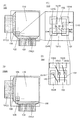
- FIG. 1A is a top view of the display device 100.
- the display device 100 includes a plurality of pixels 130 in the display unit 110.
- the display unit 110 includes a plurality of pixels 130 arranged in a matrix. Signals and power are supplied to the display unit 110 from the FPC 1 and the FPC 2 via the wiring 108.
- FIG. 1B is a top view of the display device 100A.
- the display device 100A includes a circuit 109 between the display portion 110 and the wiring 108. Signals and power are supplied to the display portion 110 and the circuit 109 from the FPC 1 or the FPC 2 through the wiring 108.
- the display device of one embodiment of the present invention can include one or both of a scan line driver circuit (gate driver) and a signal line driver circuit (source driver).
- the display device of one embodiment of the present invention can have a structure in which one or both of a gate driver and a source driver are not incorporated and a driver is externally provided.
- an IC functioning as a gate driver or a source driver can be electrically connected to a display device.
- the IC can be mounted on a display device by a COG method or a COF method.
- an FPC on which an IC is mounted, a TAB (Tape Automated Bonding) tape, a TCP, or the like can be connected to the display device.
- circuit 109 for example, one or both of a gate driver and a source driver can be applied.
- FIG. 1C illustrates a top view of the pixel 130 included in the display device 100.
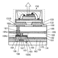
- One pixel 130 is provided with one LED package 150. That is, the display portion 110 illustrated in FIG. 1A includes a plurality of LED packages 150 provided in a matrix.
- the pixel 130 includes a conductive layer 131R, a conductive layer 131G, a conductive layer 131B, a conductive layer 132, and an LED package 150.
- FIG. 1D illustrates a top view of the LED package 150 included in the pixel 130.
- the LED package 150 has at least one LED chip.
- the LED package 150 includes a red LED chip 151R, a green LED chip 151G, and a blue LED chip 151B. That is, in the present embodiment, a configuration in which one color is represented by three sub-pixels of R (red), G (green), and B (blue) is applied to the pixel 130.
- the pixel 130 has a configuration in which one color is expressed by R, G, B, and W (white) sub-pixels, or a four-color R, G, B, and Y (yellow) sub-pixel.
- a configuration for expressing one color can be applied.
- the color elements are not limited, and colors other than RGBWY (for example, cyan or magenta) may be used.
- the LED package 150 further includes a heat sink 154, an electrode 152R, an electrode 152G, an electrode 152B, and an electrode 153.
- the red LED chip 151R is located on the electrode 152R.
- the green LED chip 151G and the blue LED chip 151B are located on the heat sink 154.
- the red LED chip 151R, the green LED chip 151G, and the blue LED chip 151B are electrically connected to the electrodes 153 via the wires 143, respectively.
- the red LED chip 151R, the green LED chip 151G, and the blue LED chip 151B include light emitting diodes that emit light of different colors. Thereby, the step of forming the color conversion layer becomes unnecessary. Therefore, the manufacturing cost of the LED chip can be reduced.
- the red LED chip 151R, the green LED chip 151G, and the blue LED chip 151B may include light emitting diodes that emit light of the same color. At this time, light emitted from the light emitting diode may be extracted to the outside of the display device via one or both of the color conversion layer and the coloring layer. One or both of the color conversion layer and the coloring layer can be provided inside or above the LED package 150.
- the display device of this embodiment may include a light-emitting diode that emits infrared light.
- a light emitting diode that emits infrared light can be used, for example, as a light source of an infrared light sensor.
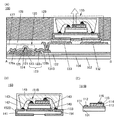
- FIG. 2A is a cross-sectional view taken along a dashed-dotted line AB in FIG. That is, FIG. 2A is a cross-sectional view including the blue LED chip 151B and the conductive layers 131B and 132 that are electrically connected to the blue LED chip 151B. Note that in FIG. 2A, some components such as wiring are omitted for clarity.
- the transistor 120 is electrically connected to the LED package 150 via the conductive layer 131B.
- the transistor 120 includes a conductive layer 121 functioning as a back gate, an insulating layer 122 functioning as a gate insulating layer, a metal oxide layer 123 functioning as a semiconductor layer (a channel formation region 123i and a pair of low-resistance regions 123n).
- the semiconductor device includes a pair of conductive layers 126a and 126b electrically connected to the region 123n, an insulating layer 124 functioning as a gate insulating layer, and a conductive layer 125 functioning as a gate.
- the conductive layer 121 and the metal oxide layer 123 overlap with the insulating layer 122 interposed therebetween.
- the conductive layer 125 and the metal oxide layer 123 overlap with the insulating layer 124 interposed therebetween.
- An insulating layer 127 is provided over the transistor 120, and a conductive layer 131B and a conductive layer 132 are provided over the insulating layer 127.
- the conductive layer 131B is electrically connected to the conductive layer 126b through an opening provided in the insulating layer 127.
- At least one of the insulating layer 124 and the insulating layer 127 is preferably formed using a material to which impurities such as water or hydrogen are unlikely to diffuse. Diffusion of impurities from the outside into the transistor can be effectively suppressed, and the reliability of the display device can be improved.
- the insulating layer 127 has a function as a planarization layer.
- a transistor 120 is provided over a substrate 102 with an insulating layer 104 interposed therebetween.
- the insulating layer 104 has a function as a base film.
- the insulating layer 104 functions as a barrier layer which prevents diffusion of impurities such as water and hydrogen from the substrate 102 into the transistor 120 and release of oxygen from the metal oxide layer 123 to the insulating layer 104 side.
- a film such as an aluminum oxide film, a hafnium oxide film, or a silicon nitride film, to which hydrogen and oxygen are less likely to diffuse than a silicon oxide film can be used.
- the transistor 120 may be formed directly over the substrate 102 without providing the insulating layer 104.
- the end of the conductive layer 131B and the end of the conductive layer 132 are covered with a protective layer 128.
- the protective layer 128 has an opening reaching the upper surface of the conductive layer 131B and an opening reaching the upper surface of the conductive layer 132. In the opening, the conductive layer 131B and the conductive layer 132 are electrically connected to the LED package 150 via the conductor 133, respectively.
- the protective layer 1208 As a material of the protective layer 128, a resin such as acrylic, polyimide, epoxy, or silicone is preferable. With the provision of the protective layer 128, the conductor 133 on the conductive layer 131B and the conductor 133 on the conductive layer 132 can be prevented from being short-circuited due to contact. Note that the protective layer 128 need not be provided.
- each of the conductive layers 131R, 131G, 131B, and 132 connected to the conductor 133 and the electrodes 152R, 152G, 152B, and 153 be formed using a conductive material having low contact resistance with the conductor 133.
- the conductive material connected thereto is aluminum, titanium, copper, an alloy of silver (Ag), palladium (Pd), and copper (Cu) (Ag-Pd-Cu ( APC)) and the like are preferable because the contact resistance is low.
- the conductor 133 may be provided on the substrate 102 or may be provided on the LED package 150 side. For example, mounting the LED package 150 on the substrate 102 by providing the conductor 133 on each of the conductive layers 131R, 131G, 131B, and 132, and then connecting the conductor 133 and the LED package 150. Can be.
- a plurality of light-emitting diodes may be electrically connected to one transistor.
- the side surface of the LED package 150 may be covered with the resin 129. It is preferable to use a black resin as the resin 129 because display contrast can be increased. Further, a surface protection layer, a shock absorbing layer, and the like may be provided on the upper surface of the LED package 150. Since the LED package 150 is configured to extract light upward, it is preferable that a layer provided on the upper surface of the LED package 150 has transparency to visible light.
- an insulating substrate such as a glass substrate, a quartz substrate, a sapphire substrate, or a ceramic substrate, a single crystal semiconductor substrate made of silicon, silicon carbide, or the like, a polycrystalline semiconductor substrate, or a compound semiconductor substrate such as silicon germanium And a semiconductor substrate such as an SOI substrate.
- the substrate 102 preferably blocks visible light (has non-transparency with respect to visible light). When the substrate 102 blocks visible light, light can be prevented from entering the transistor 120 formed over the substrate 102 from the outside. Note that one embodiment of the present invention is not limited thereto, and the substrate 102 may have a property of transmitting visible light.
- the substrate 102 may include one or both of a reflective layer that reflects light of the light emitting diode and a light blocking layer that blocks the light.
- the plurality of light emitting diodes (LED chips) included in the LED package 150 may be driven by transistors having the same configuration, or may be driven by transistors having different configurations.
- a transistor for driving the red LED chip 151R, a transistor for driving the green LED chip 151G, and a transistor for driving the blue LED chip 151B include a transistor size, a channel length, a channel width, a structure, and the like. May be different from each other. Specifically, one or both of the channel length and the channel width of the transistor may be changed for each color in accordance with the amount of current required to emit light with desired luminance.
- materials that can be used for various conductive layers included in the display device of this embodiment include metals such as aluminum, titanium, chromium, nickel, copper, yttrium, zirconium, molybdenum, silver, tantalum, and tungsten; Alternatively, an alloy containing this as a main component may be used. Further, a film containing any of these materials can be used as a single layer or a stacked structure. For example, a single-layer structure of an aluminum film containing silicon, a two-layer structure of stacking an aluminum film on a titanium film, a two-layer structure of stacking an aluminum film on a tungsten film, and a copper film on a copper-magnesium-aluminum alloy film.
- a two-layer structure in which a copper film is stacked on a titanium film a two-layer structure in which a copper film is stacked on a tungsten film, a titanium film or a titanium nitride film, and an aluminum film or a copper film stacked thereon
- an oxide such as indium oxide, tin oxide, or zinc oxide may be used.
- it is preferable to use copper containing manganese since the controllability of the shape by etching is improved.
- materials that can be used for various insulating layers included in the display device of this embodiment include resins such as acrylic, polyimide, epoxy, and silicone; silicon oxide; silicon oxynitride; silicon nitride oxide; silicon nitride; An inorganic insulating material such as aluminum is used.
- the LED package 150 will be described in more detail with reference to FIG. Further, the blue LED chip 151B will be described in more detail with reference to FIG.
- the LED package 150 illustrated in FIG. 2B includes a substrate 141, a blue LED chip 151B, an electrode 152B, an electrode 153, a heat sink 154, an adhesive layer 146, a case 142, a wire 143, a wire 144, and a sealing layer 145. .
- the blue LED chip 151B is attached on the substrate 141 by the adhesive layer 146.
- the blue LED chip 151B is provided so as to overlap the heat sink 154 via the adhesive layer 146.
- the material of the adhesive layer 146 is not particularly limited. However, as described later, the red LED chip 151R is bonded to the electrode 152R so as to be electrically connected to the electrode 152R. Then, the material of the adhesive layer 146 can be made uniform for the LED chips of each color, which is preferable. Further, in the blue LED chip and the green LED chip, it is preferable to use a conductive adhesive as the adhesive layer 146 because heat dissipation is improved.
- the heat sink 154 can be formed using the same material and the same process as the electrodes 152B and 153.
- a glass epoxy resin substrate a polyimide substrate, a ceramic substrate, an alumina substrate, an aluminum nitride substrate, or the like can be used.
- the blue LED chip 151B illustrated in FIG. 2C has a structure in which a light-emitting diode (LED) is provided over a substrate 101.
- the light-emitting diode includes a semiconductor layer 111, an electrode 112, a light-emitting layer 113, a semiconductor layer 114, an electrode 115, and an electrode 116.
- the electrode 112 is electrically connected to the semiconductor layer 111.
- the electrode 116 is electrically connected to the semiconductor layer 114 through the electrode 115. Only one of the electrode 115 and the electrode 116 may be provided.
- the light emitting layer 113 is sandwiched between the semiconductor layers 111 and 114. In the light emitting layer 113, electrons and holes are combined to emit light.
- One of the semiconductor layer 111 and the semiconductor layer 114 is an n-type semiconductor layer, and the other is a p-type semiconductor layer.
- a stacked structure including the semiconductor layer 111, the light emitting layer 113, and the semiconductor layer 114 is formed so as to emit blue light.
- each light-emitting diode a stacked structure including a pair of semiconductor layers and a light-emitting layer between the pair of semiconductor layers is formed to emit light of red, yellow, green, or blue, or the like.
- the laminated structure includes, for example, a gallium / phosphorus compound, a gallium / arsenic compound, a gallium / aluminum / arsenic compound, an aluminum / gallium / indium / phosphorous compound, a gallium nitride, an indium / gallium nitride compound, a selenium / zinc compound, and the like. Can be used.
- a single crystal substrate such as a sapphire (Al 2 O 3 ) substrate, a silicon carbide (SiC) substrate, a silicon (Si) substrate, and a gallium nitride (GaN) substrate can be used.
- the electrode 112 is electrically connected to the electrode 152B via the wire 143.
- the electrode 112 functions as a pixel electrode of the light emitting diode.
- the electrode 116 is electrically connected to the electrode 153 via the wire 144.
- the electrode 116 functions as a common electrode of the light emitting diode.
- Each of the electrode 152B and the electrode 153 can be formed using one element selected from nickel, copper, silver, platinum, and gold, or an alloy material containing 50% or more of the element.
- connection between the electrode 152B and the electrode 112 and the connection between the electrode 153 and the electrode 116 can be performed by a wire bonding method using a thermocompression bonding method or an ultrasonic bonding method, respectively.
- each of the wires 143 and 144 a thin metal wire formed of gold, an alloy containing gold, copper, an alloy containing copper, or the like can be used.
- the case 142 As the material of the case 142, a resin can be used.
- the case 142 only needs to cover at least the side surface of the blue LED chip 151B, and does not have to overlap the upper surface of the blue LED chip 151B.
- the sealing layer 145 may be exposed on the upper surface side of the blue LED chip 151B. It is preferable to provide a reflector made of ceramic or the like on the inner side surface of the case 142, specifically, around the blue LED chip 151B. A part of the light emitted by the blue LED chip 151B is reflected by the reflector, so that more light can be extracted from the LED package 150.
- the inside of the case 142 is filled with a sealing layer 145.
- a resin having transparency to visible light is preferable.
- an ultraviolet curable resin such as an epoxy resin or a silicone resin, a visible light curable resin, or the like can be used.
- FIG. 3A is a cross-sectional view taken along dashed-dotted line CD in FIG. 1C. That is, FIG. 3A is a cross-sectional view including the red LED chip 151R, and the conductive layers 131R and 132 electrically connected to the red LED chip 151R. Note that in FIG. 3A, some components such as wiring are omitted for clarity.
- the transistor 120A is electrically connected to the LED package 150 via the conductive layer 131R.
- the transistor 120A has a structure similar to that of the transistor 120 illustrated in FIG. 2A, and thus detailed description is omitted.
- An insulating layer 127 is provided over the transistor 120A, and a conductive layer 131R and a conductive layer 132 are provided over the insulating layer 127.
- the conductive layer 131R is electrically connected to the conductive layer 126b through an opening provided in the insulating layer 127.
- the conductive layer 131R and the conductive layer 132 are each electrically connected to the LED package 150 via the conductor 133.
- the LED package 150 will be described in more detail with reference to FIG. Further, the red LED chip 151R will be described in more detail with reference to FIG.
- the LED package 150 illustrated in FIG. 3B includes a substrate 141, a red LED chip 151R, an electrode 152R, an electrode 153, an adhesive layer 146, a case 142, a wire 144, and a sealing layer 145.
- the red LED chip 151R is electrically connected to the electrode 152R via a conductive adhesive layer 146.
- the red LED chip 151R illustrated in FIG. 3C includes the electrode 103, the semiconductor layer 117, the light-emitting layer 118, the semiconductor layer 119, and the electrode 106.
- the red LED chip 151R can also be called a light emitting diode (LED). Further, the red LED chip may have a configuration in which a light emitting diode is provided on a conductive substrate.
- the electrode 103 is electrically connected to the semiconductor layer 117.
- the electrode 106 is electrically connected to the semiconductor layer 119.
- the light-emitting layer 118 is sandwiched between the semiconductor layers 117 and 119. In the light emitting layer 118, electrons and holes are combined to emit light.
- One of the semiconductor layer 117 and the semiconductor layer 119 is an n-type semiconductor layer, and the other is a p-type semiconductor layer.
- the electrode 103 is electrically connected to the electrode 152R via the adhesive layer 146.
- the electrode 103 functions as a pixel electrode of the light emitting diode.
- the electrode 106 is electrically connected to the electrode 153 via the wire 144.
- the electrode 106 functions as a common electrode of the light emitting diode.
- a color conversion layer 147 may be provided inside the case 142.
- the light of the light emitting diode is emitted to the outside of the LED package 155 via the color conversion layer 147.
- FIG. 3D illustrates a structure in which the color conversion layer 147 is provided over the sealing layer 145; however, the arrangement of the color conversion layer 147 is not limited to this.
- the color conversion layer 147 may be dispersed inside the sealing layer 145.
- quantum dots have narrow emission spectrum peak widths and can emit light with good color purity. Thereby, the display quality of the display device can be improved.
- the color conversion layer 147 is preferably provided inside or above the LED package 155.
- a color conversion layer 147 for converting blue light to red is provided at a position overlapping the red LED chip 151R, and a color for converting blue light to green is provided at a position overlapping the green LED chip 151G.
- a conversion layer 147 is provided.
- the light emitted from the light emitting diode is converted from blue to red by the color conversion layer 147 and emitted to the outside of the display device.
- the green sub-pixel light emitted from the light-emitting diode is converted from blue to green by the color conversion layer 147 and emitted to the outside of the display device.
- the blue sub-pixel the blue light emitted from the light emitting diode is directly emitted to the outside of the display device.
- the color conversion layer 147 can be formed by a droplet discharge method (for example, an inkjet method), a coating method, an imprint method, various printing methods (screen printing, offset printing), or the like. Further, a color conversion film such as a quantum dot film may be used.
- a droplet discharge method for example, an inkjet method
- a coating method for example, an imprint method
- various printing methods screen printing, offset printing
- a color conversion film such as a quantum dot film may be used.
- an organic resin layer having a surface printed or painted with the phosphor, an organic resin layer in which the phosphor is mixed, or the like can be used.
- the material constituting the quantum dot is not particularly limited, and may be, for example, a group 14 element, a group 15 element, a group 16 element, a compound comprising a plurality of group 14 elements, or a group 4 to group 14 element.
- a compound of an element and a group 16 element, a compound of a group 2 element and a group 16 element, a compound of a group 13 element and a group 15 element, a compound of a group 13 element and a group 17 element examples include a compound of a Group 14 element and a Group 15 element, a compound of a Group 11 element and a Group 17 element, iron oxides, titanium oxides, chalcogenide spinels, and semiconductor clusters.
- quantum dots examples include a core type, a core-shell type, and a core-multi-shell type.
- quantum dots have a high ratio of surface atoms, and therefore have high reactivity and are likely to aggregate. Therefore, it is preferable that a protective agent is attached to the surface of the quantum dot or a protective group is provided. When the protective agent is attached or the protective group is provided, aggregation can be prevented and solubility in a solvent can be increased. It is also possible to reduce reactivity and improve electrical stability.
- the size of the quantum dot is appropriately adjusted so that light of a desired wavelength is obtained.
- the emission of the quantum dot shifts to the blue side, that is, to the higher energy side.
- the size (diameter) of the quantum dot is, for example, 0.5 nm or more and 20 nm or less, preferably 1 nm or more and 10 nm or less.
- the shape of the quantum dot is not particularly limited, and may be spherical, rod-shaped, disk-shaped, or other shapes.
- a quantum rod, which is a rod-like quantum dot, has a function of exhibiting directional light.
- a stacked structure of the color conversion layer 147 and the coloring layer may be provided inside or above the LED package 155. Accordingly, the light converted by the color conversion layer 147 passes through the coloring layer, so that the purity of the light can be increased.
- a blue colored layer may be provided at a position overlapping with the blue LED chip 151B. When a blue coloring layer is provided, the purity of blue light can be increased. When a blue colored layer is not provided, the manufacturing process can be simplified.
- the coloring layer is a colored layer that transmits light in a specific wavelength range.
- a color filter that transmits light in a red, green, blue, or yellow wavelength range can be used.
- a material that can be used for the coloring layer a metal material, a resin material, a resin material containing a pigment or a dye, or the like can be given.
- [Configuration Example 2 of Display Device] 4 to 6 show cross-sectional configuration examples of the display device, which are different from the first configuration example of the display device.
- the display devices illustrated in FIGS. 4 to 6 are different from FIG. 2A mainly in the structure of a transistor electrically connected to the LED package 150.
- the transistor 120B is electrically connected to the LED package 150 through the conductive layer 131B.
- the transistor 120B includes a conductive layer 121 functioning as a gate, an insulating layer 122 functioning as a gate insulating layer, a metal oxide layer 123 functioning as a semiconductor layer, a pair of conductive layers 126a and 126b functioning as a source and a drain, and a gate insulating layer. Insulating layers 124a and 124b functioning as a gate, and a conductive layer 125 functioning as a back gate.
- the conductive layer 121 and the metal oxide layer 123 overlap with the insulating layer 122 interposed therebetween.
- the conductive layer 125 and the metal oxide layer 123 overlap with each other with the insulating layer 124a and the insulating layer 124b interposed therebetween.
- An insulating layer 127 is provided over the transistor 120B, and a conductive layer 131B and a conductive layer 132 are provided over the insulating layer 127.
- the conductive layer 131B is electrically connected to the conductive layer 126b through an opening provided in the insulating layer 127.
- the transistor 120C is electrically connected to the LED package 150 through the conductive layer 131B and the like.
- An insulating layer 175, a transistor 120C, a conductive layer 184a, a conductive layer 184b, a conductive layer 187, a conductive layer 189, an insulating layer 186, an insulating layer 188, a conductive layer 131B, a conductive layer 132, and the like are provided over the substrate 174. ing. On the substrate 174, insulating layers such as an insulating layer 162, an insulating layer 181, an insulating layer 182, an insulating layer 183, and an insulating layer 185 are provided. One or more of these insulating layers may be regarded as a component of the transistor in some cases; however, in this embodiment, description will be made without including the component in the transistor.
- an insulating substrate such as a glass substrate, a quartz substrate, a sapphire substrate, or a ceramic substrate, a single crystal semiconductor substrate made of a material such as silicon or silicon carbide, a polycrystalline semiconductor substrate, or a compound semiconductor substrate such as silicon germanium And a semiconductor substrate such as an SOI substrate.
- the substrate 151 preferably blocks visible light (has non-transparency with respect to visible light). When the substrate 151 blocks visible light, light can be prevented from entering the transistor 120C formed in the substrate 151 from the outside. Note that one embodiment of the present invention is not limited thereto, and the substrate 151 may have a property of transmitting visible light.
- An insulating layer 175 is provided over the substrate 174.
- the insulating layer 175 functions as a barrier layer that prevents impurities such as water and hydrogen from diffusing from the substrate 174 into the transistor 120C and preventing oxygen from being released from the metal oxide layer 165 to the insulating layer 175 side.
- a film such as an aluminum oxide film, a hafnium oxide film, or a silicon nitride film, to which hydrogen and oxygen are less likely to diffuse than a silicon oxide film can be used.
- the transistor 120C includes a conductive layer 161, an insulating layer 163, an insulating layer 164, a metal oxide layer 165, a pair of conductive layers 166, an insulating layer 167, a conductive layer 168, and the like.
- the metal oxide layer 165 has a channel formation region.
- the metal oxide layer 165 includes a first region overlapping with one of the pair of conductive layers 166, a second region overlapping with the other of the pair of conductive layers 166, and a region between the first region and the second region. And a third region.
- a conductive layer 161 and an insulating layer 162 are provided over the insulating layer 175, and an insulating layer 163 and an insulating layer 164 are provided so as to cover the conductive layer 161 and the insulating layer 162.
- the metal oxide layer 165 is provided over the insulating layer 164.
- the conductive layer 161 functions as a gate electrode, and the insulating layers 163 and 164 function as gate insulating layers.
- the conductive layer 161 overlaps with the metal oxide layer 165 with the insulating layer 163 and the insulating layer 164 interposed therebetween.
- the insulating layer 163 preferably functions as a barrier layer, similarly to the insulating layer 175.
- an oxide insulating film such as a silicon oxide film is preferably used.
- the height of the upper surface of the conductive layer 161 is approximately equal to the height of the upper surface of the insulating layer 162.
- an opening is provided in the insulating layer 162, the conductive layer 161 is formed so as to fill the opening, and then planarization is performed by a CMP method or the like, so that the height of the upper surface of the conductive layer 161 and the height of the insulating layer 162 are reduced.
- the height of the upper surface can be made uniform.
- the size of the transistor 120C can be reduced.
- the pair of conductive layers 166 is provided separately over the metal oxide layer 165.
- the pair of conductive layers 166 functions as a source and a drain.
- An insulating layer 181 is provided so as to cover the metal oxide layer 165 and the pair of conductive layers 166.
- An insulating layer 182 is provided over the insulating layer 181.
- An opening reaching the metal oxide layer 165 is provided in the insulating layers 181 and 182, and the insulating layer 167 and the conductive layer 168 are embedded in the openings. The opening overlaps the third region.
- the insulating layer 167 overlaps with a side surface of the insulating layer 181 and a side surface of the insulating layer 182.
- the conductive layer 168 overlaps with a side surface of the insulating layer 181 and a side surface of the insulating layer 182 with the insulating layer 167 provided therebetween.
- the conductive layer 168 functions as a gate electrode, and the insulating layer 167 functions as a gate insulating layer.
- the conductive layer 168 overlaps with the metal oxide layer 165 with the insulating layer 167 provided therebetween.
- the height of the upper surface of the conductive layer 168 is approximately equal to the height of the upper surface of the insulating layer 182.
- an opening is provided in the insulating layer 182, the insulating layer 167 and the conductive layer 168 are formed so as to fill the opening, and then planarization treatment is performed, so that the height of the upper surface of the conductive layer 168 and the height of the upper surface of the insulating layer 182 are reduced. Height can be aligned. Thus, the size of the transistor 120C can be reduced.
- an insulating layer 183 and an insulating layer 185 are provided so as to cover upper surfaces of the insulating layer 182, the insulating layer 167, and the conductive layer 168.
- the insulating layers 181 and 183 preferably function as barrier layers, similarly to the insulating layer 175.
- a plug electrically connected to one of the pair of conductive layers 166 and the conductive layer 187 is embedded in an opening provided in the insulating layer 181, the insulating layer 182, the insulating layer 183, and the insulating layer 185.
- the plug preferably has a conductive layer 184a in contact with a side surface of the opening and one upper surface of the pair of conductive layers 166, and a conductive layer 184b embedded inside the conductive layer 184a.
- the conductive layer 184a is preferably formed using a conductive material to which hydrogen and oxygen are unlikely to diffuse.
- the conductive layer 187 is provided over the insulating layer 185, and the insulating layer 186 is provided over the conductive layer 187.
- An opening reaching the conductive layer 187 is provided in the insulating layer 186, and the conductive layer 189 is embedded in the opening.
- the conductive layer 189 functions as a plug that electrically connects the conductive layer 187 and the conductive layer 131B.
- One of the pair of conductive layers 166 is electrically connected to the conductive layer 131B through the conductive layers 184a, 184b, 187, and 189.
- the height of the upper surface of the conductive layer 161 is approximately equal to the height of the upper surface of the insulating layer 162.
- the height of the upper surface of the conductive layer 168 is approximately equal to the height of the upper surface of the insulating layer 182.
- the display device of this embodiment include a transistor in which the height of the upper surface of the gate electrode is approximately equal to the height of the upper surface of the insulating layer.
- the upper surface of the gate electrode and the upper surface of the insulating layer are flattened, and the height of the upper surface of the gate electrode is made equal to the height of the upper surface of the insulating layer. be able to.
- the transistor having such a structure can be easily reduced in size. Since the size of the pixel can be reduced by reducing the size of the transistor, the definition of the display device can be increased.
- the transistor 120C is electrically connected to the LED package 150 through the conductive layer 131B and the like.
- the display device illustrated in FIG. 6 includes a stack of a transistor 190 having a channel formation region over a substrate 191 and a transistor 120C having a channel formation region over a metal oxide.
- the transistor 190 includes a conductive layer 195, an insulating layer 194, an insulating layer 196, and a pair of low-resistance regions 193.
- the conductive layer 195 functions as a gate.
- the insulating layer 194 is located between the conductive layer 195 and the substrate 191, and functions as a gate insulating layer.
- the insulating layer 196 is provided to cover a side surface of the conductive layer 195 and functions as a sidewall.
- the pair of low-resistance regions 193 is a region of the substrate 191 to which an impurity is doped, and one functions as a source of the transistor 190 and the other functions as a drain of the transistor 190.
- an element isolation layer 192 is provided between two adjacent transistors so as to be embedded in the substrate 191.
- An insulating layer 199 is provided to cover the transistor 190, and a conductive layer 198 is provided over the insulating layer 199. Through the opening in the insulating layer 199, the conductive layer 198 is electrically connected to one of the pair of low-resistance regions 193.
- An insulating layer 171 is provided to cover the conductive layer 198, and a conductive layer 172 is provided over the insulating layer 171.
- the conductive layers 198 and 172 each function as a wiring.
- An insulating layer 173 and an insulating layer 175 are provided to cover the conductive layer 172, and the transistor 120C is provided over the insulating layer 175. Since the laminated structure from the insulating layer 175 to the LED package 150 is the same as that of the display device shown in FIG. 5, detailed description will be omitted.
- the transistor 120C can be used as a transistor included in a pixel circuit.
- the transistor 190 can be used as a transistor included in a pixel circuit or a transistor included in a driver circuit for driving the pixel circuit (one or both of a gate driver and a source driver).
- the transistor 120C and the transistor 190 can be used as transistors included in various circuits such as an arithmetic circuit and a memory circuit, respectively.
- a pixel circuit not only a pixel circuit but also a driver circuit and the like can be formed directly below the light-emitting diode, so that the size of the display device is reduced as compared to a case where a driver circuit is provided outside the display portion. be able to. Further, a display device with a narrow frame (a narrow non-display area) can be realized.
- the display device of one embodiment of the present invention may be a display device provided with a touch sensor (also referred to as an input / output device or a touch panel).
- a touch sensor also referred to as an input / output device or a touch panel.
- the configuration of each display device described above can be applied to a touch panel.
- sensing element also referred to as a sensor element
- Various sensors capable of detecting the proximity or contact of a detection target such as a finger or a stylus can be applied as the detection element.
- a sensor system various systems such as a capacitance system, a resistive film system, a surface acoustic wave system, an infrared system, an optical system, and a pressure-sensitive system can be used.
- Examples of the capacitance type include a surface type capacitance type and a projection type capacitance type.
- the projection type capacitance method there are a self capacitance method, a mutual capacitance method, and the like. It is preferable to use the mutual capacitance method because simultaneous multipoint detection becomes possible.
- the touch panel of one embodiment of the present invention has a structure in which a display device and a sensing element which are separately manufactured are bonded to each other, an electrode which forms a sensing element is provided on one or both of a substrate supporting the display element and a counter substrate, or the like.
- Various configurations can be applied.
- the display device of this embodiment can be manufactured by mounting an LED package on a substrate over which a plurality of transistors are formed, the difficulty in manufacturing the display device is reduced and the yield is improved. Can be planned.
- a display device with reduced power consumption can be realized by combining a micro LED with a transistor including a metal oxide.
- the size of the transistor can be reduced in the display device of this embodiment, the definition can be easily increased and application to an electronic device having a relatively small display portion can be easily performed.
- the display device of this embodiment includes a plurality of pixels arranged in a matrix of m rows and n columns (m and n are each an integer of 1 or more).
- FIG. 7 illustrates an example of a circuit diagram of a pixel 200 (i, j) (i is an integer of 1 to m, and j is an integer of 1 to n).
- the pixel 200 (i, j) illustrated in FIG. 7 includes a light-emitting element 210, a switch SW21, a switch SW22, a transistor M, and a capacitor C1.
- the gate of the switch SW21 is electrically connected to the scanning line GL1 (i).
- One of a source and a drain of the switch SW21 is electrically connected to the signal line SL (j), and the other is electrically connected to the gate of the transistor M.
- the gate of the switch SW22 is electrically connected to the scanning line GL2 (i).
- One of a source and a drain of the switch SW22 is electrically connected to the wiring COM, and the other is electrically connected to a gate of the transistor M.
- the gate of the transistor M is electrically connected to one electrode of the capacitor C1, the other of the source and the drain of the switch SW21, and the other of the source and the drain of the switch SW22.
- One of a source and a drain of the transistor M is electrically connected to the wiring CATHODE, and the other is electrically connected to a cathode of the light-emitting element 210.
- the other electrode of the capacitor C1 is electrically connected to the wiring CATHODE.
- the anode of the light-emitting element 210 is electrically connected to the wiring ANODE.
- the scanning line GL1 (i) has a function of supplying a selection signal.
- the scanning line GL2 (i) has a function of supplying a control signal.
- the signal line SL (j) has a function of supplying an image signal.
- a constant potential is supplied to the wiring VCOM, the wiring CATHODE, and the wiring ANODE.
- the anode side of the light emitting element 210 can be set to a high potential, and the cathode side can be set to a lower potential than the anode side.
- the switch SW21 is controlled by a selection signal and functions as a selection transistor for controlling the selection state of the pixel 200.
- the transistor M functions as a driving transistor that controls a current flowing to the light-emitting element 210 according to a potential supplied to a gate.
- the switch SW21 When the switch SW21 is on, the image signal supplied to the signal line SL (j) is supplied to the gate of the transistor M, and the luminance of the light emitting element 210 can be controlled in accordance with the potential.
- the switch SW22 has a function of controlling the gate potential of the transistor M based on a control signal. Specifically, the switch SW22 can supply a potential which makes the transistor M non-conductive to the gate of the transistor M.
- the switch SW22 can be used for controlling a pulse width, for example.
- a current can be supplied from the transistor M to the light-emitting element 210 during a period based on the control signal.
- the light emitting element 210 can express a gray scale based on an image signal and a control signal.
- a transistor including a metal oxide (oxide semiconductor) for a semiconductor layer in which a channel is formed is preferably used.
- a transistor including a metal oxide with a wider band gap and lower carrier density than silicon can achieve extremely low off-state current. Therefore, with the small off-state current, electric charge accumulated in a capacitor connected in series with the transistor can be held for a long time. Therefore, it is particularly preferable to use a transistor to which an oxide semiconductor is applied for the switches SW21 and SW22 connected in series to the capacitor C1. In addition, by using a transistor to which an oxide semiconductor is similarly applied for other transistors, manufacturing cost can be reduced.
- the transistor included in the pixel 200 (i, j) a transistor in which silicon is used for a semiconductor in which a channel is formed can be used. It is particularly preferable to use silicon having high crystallinity, such as single crystal silicon or polycrystalline silicon, because high field-effect mobility can be realized and higher-speed operation can be performed.
- a transistor including an oxide semiconductor may be used for at least one of the transistors, and a transistor including silicon may be used for the other transistors.
- the transistor is described as an n-channel transistor; however, a p-channel transistor can be used.
- Transistor Next, a transistor that can be used for a display device is described.
- the structure of the transistor included in the display device is not particularly limited.
- a planar transistor, a staggered transistor, or an inverted staggered transistor may be used.
- a top gate structure or a bottom gate structure may be employed.
- gate electrodes may be provided above and below a channel.
- a transistor included in the display device for example, a transistor including a metal oxide for a channel formation region can be used. Thus, a transistor with extremely low off-state current can be realized.
- a transistor including silicon in a channel formation region may be used as a transistor included in the display device.
- the transistor include a transistor including amorphous silicon, a transistor including crystalline silicon (typically, low-temperature polysilicon), and a transistor including single crystal silicon.
- Metal oxide Hereinafter, a metal oxide applicable to the semiconductor layer will be described.
- the metal oxide preferably contains at least indium or zinc. In particular, it preferably contains indium and zinc. In addition, it is preferable that aluminum, gallium, yttrium, tin, or the like be contained in addition thereto. In addition, one or more kinds selected from boron, titanium, iron, nickel, germanium, zirconium, molybdenum, lanthanum, cerium, neodymium, hafnium, tantalum, tungsten, magnesium, and the like may be included.
- the metal oxide is an In-M-Zn oxide including indium, the element M, and zinc is considered.
- the element M is aluminum, gallium, yttrium, tin, or the like.
- Other elements applicable to the element M include boron, titanium, iron, nickel, germanium, zirconium, molybdenum, lanthanum, cerium, neodymium, hafnium, tantalum, tungsten, and magnesium.
- a combination of a plurality of the aforementioned elements may be used as the element M.
- the metal oxide film can be formed by a sputtering method.
- a PLD method a PECVD method, a thermal CVD method, an ALD method, a vacuum evaporation method, or the like may be used.
- a metal oxide containing nitrogen may be collectively referred to as a metal oxide (metal oxide). Further, a metal oxide containing nitrogen may be referred to as metal oxynitride. For example, a metal oxide containing nitrogen such as zinc oxynitride (ZnON) may be used for the semiconductor layer.
- metal oxide metal oxide
- ZnON zinc oxynitride
- CAAC c-axis @ aligned crystal
- CAC Cloud-Aligned @ Composite
- CAC Cloud-Aligned @ Composite
- OS can be used for the semiconductor layer.
- the CAC-OS or CAC-metal oxide includes a conductive function in part of a material, an insulating function in part of a material, and a semiconductor function as a whole of the material.
- a conductive function is a function of flowing electrons (or holes) serving as carriers
- an insulating function is a function of flowing electrons serving as carriers. It is a function that does not flow.
- the CAC-OS or CAC-metal oxide includes a conductive region and an insulating region.
- the conductive region has the above-described conductive function
- the insulating region has the above-described insulating function.
- a conductive region and an insulating region are separated at a nanoparticle level in a material. Further, the conductive region and the insulating region may be unevenly distributed in the material. In some cases, the conductive region is observed with its periphery blurred and connected in a cloud shape.
- the conductive region and the insulating region each have a size of 0.5 nm to 10 nm, preferably 0.5 nm to 3 nm, and are dispersed in a material. There is.
- CAC-OS or CAC-metal oxide includes components having different band gaps.
- a CAC-OS or a CAC-metal oxide includes a component having a wide gap due to an insulating region and a component having a narrow gap due to a conductive region.
- the carrier when the carrier flows, the carrier mainly flows in the component having the narrow gap.
- the component having the narrow gap acts complementarily to the component having the wide gap, and the carrier flows to the component having the wide gap in conjunction with the component having the narrow gap. Therefore, in the case where the CAC-OS or CAC-metal oxide is used for a channel formation region of a transistor, high current driving capability, that is, a high on-state current and high field-effect mobility can be obtained when the transistor is on.
- CAC-OS or the CAC-metal oxide may be referred to as a matrix composite (metal @ composite) or a metal matrix composite (metal @ matrix @ composite).
- An oxide semiconductor is classified into a single crystal oxide semiconductor and a non-single-crystal oxide semiconductor.
- a non-single-crystal oxide semiconductor for example, a CAAC-OS (c-axis aligned crystalline oxide semiconductor), a polycrystalline oxide semiconductor, an nc-OS (nanocrystalline oxide semiconductor), and a pseudo-amorphous oxide semiconductor (a-like) OS: amorphous-like oxide semiconductor, an amorphous oxide semiconductor, or the like.
- the CAAC-OS has a c-axis orientation and a crystal structure in which a plurality of nanocrystals are connected in an ab plane direction and has a strain.
- the strain refers to a region where the orientation of the lattice arrangement changes between a region where the lattice arrangement is uniform and a region where another lattice arrangement is uniform in a region where a plurality of nanocrystals are connected.
- the nanocrystal is basically a hexagon, but is not limited to a regular hexagon and may be a non-regular hexagon.
- distortion may have a lattice arrangement such as a pentagon and a heptagon.
- a clear crystal grain boundary also referred to as a grain boundary
- the formation of crystal grain boundaries is suppressed by the distortion of the lattice arrangement. This is because the CAAC-OS can tolerate distortion because the arrangement of oxygen atoms is not dense in the ab plane direction, or the bonding distance between atoms changes by substitution with a metal element. That's why.
- the CAAC-OS is a layered crystal in which a layer containing indium and oxygen (hereinafter, an In layer) and a layer containing elements M, zinc, and oxygen (hereinafter, an (M, Zn) layer) are stacked. It tends to have a structure (also called a layered structure).
- indium and the element M can be replaced with each other, and when the element M in the (M, Zn) layer is replaced with indium, it can also be referred to as an (In, M, Zn) layer.
- indium in the In layer is replaced with the element M, it can be referred to as an (In, M) layer.
- CAAC-OS is a metal oxide with high crystallinity.
- CAAC-OS it is difficult to confirm a clear crystal grain boundary; thus, it can be said that electron mobility due to the crystal grain boundary is not easily reduced.
- CAAC-OS impurities and defects oxygen deficiency (V O:. Oxygen vacancy also referred) etc.) with less metal It can also be called an oxide. Therefore, a metal oxide having a CAAC-OS has stable physical properties. Therefore, the metal oxide including the CAAC-OS is resistant to heat and has high reliability.
- the nc-OS has a periodic atomic arrangement in a minute region (for example, a region with a thickness of 1 nm to 10 nm, particularly, a region with a size of 1 nm to 3 nm).
- a minute region for example, a region with a thickness of 1 nm to 10 nm, particularly, a region with a size of 1 nm to 3 nm.
- the nc-OS may not be distinguished from an a-like @ OS or an amorphous oxide semiconductor depending on an analysis method.
- indium-gallium-zinc oxide which is a kind of metal oxide including indium, gallium, and zinc
- IGZO indium-gallium-zinc oxide
- a smaller crystal for example, the above-described nanocrystal
- a large crystal here, a crystal of several mm or a crystal of several cm.
- it may be structurally stable.
- a-like @ OS is a metal oxide having a structure between an nc-OS and an amorphous oxide semiconductor.
- a-like @ OS has voids or low density regions. That is, a-like @ OS has lower crystallinity than the nc-OS and the CAAC-OS.
- Oxide semiconductors have various structures and each have different characteristics.
- the oxide semiconductor of one embodiment of the present invention may include two or more of an amorphous oxide semiconductor, a polycrystalline oxide semiconductor, an a-like @ OS, an nc-OS, and a CAAC-OS.
- the metal oxide film functioning as a semiconductor layer can be formed using one or both of an inert gas and an oxygen gas.
- an inert gas an oxygen gas
- an oxygen gas an oxygen gas
- the flow rate ratio of oxygen (oxygen partial pressure) at the time of forming the metal oxide film is preferably 0% or more and 30% or less, and 5% or more and 30% or less. Is more preferable, and 7% or more and 15% or less are still more preferable.
- the metal oxide preferably has an energy gap of 2 eV or more, more preferably 2.5 eV or more, and still more preferably 3 eV or more.
- the electronic device of this embodiment includes the display device of one embodiment of the present invention in the display portion.
- the display device of one embodiment of the present invention has high display quality and low power consumption.
- the display device of one embodiment of the present invention can easily have high definition and large size. Therefore, it can be used for display portions of various electronic devices.
- Examples of the electronic device include a television device, a desktop or notebook personal computer, a monitor for a computer, a digital signage, an electronic device having a relatively large screen such as a large game machine such as a pachinko machine, and a digital device.
- Examples include a camera, a digital video camera, a digital photo frame, a mobile phone, a portable game machine, a portable information terminal, and a sound reproducing device.
- the display device of one embodiment of the present invention can have higher definition and can be preferably used for an electronic device having a relatively small display portion.
- electronic devices include wristwatch-type or bracelet-type information terminals (wearable devices), devices for VR (Virtual Reality) such as head-mounted displays, glasses-type devices for AR (Augmented Reality), and MR. (Mixed Reality) and other wearable devices that can be worn on the head.
- the electronic device includes sensors (force, displacement, position, speed, acceleration, angular velocity, rotation speed, distance, light, liquid, magnetism, temperature, chemical substance, sound, time, hardness, electric field, current, voltage Including a function of measuring power, radiation, flow rate, humidity, gradient, vibration, smell or infrared light).
- the electronic device of this embodiment can have various functions. For example, a function of displaying various information (still images, moving images, text images, etc.) on the display unit, a touch panel function, a function of displaying a calendar, date or time, a function of executing various software (programs), a wireless communication It can have a function, a function of reading a program or data recorded on a recording medium, and the like.
- FIG. 8A is a perspective view of a glasses-type electronic device 900.
- the electronic device 900 includes a pair of display panels 901, a pair of housings 902, a pair of optical members 903, a pair of mounting portions 904, and the like.
- the electronic device 900 can project an image displayed on the display panel 901 onto a display area 906 of the optical member 903. Since the optical member 903 has a light-transmitting property, a user can see an image displayed in the display area 906 in a manner superimposed on a transmitted image visually recognized through the optical member 903. Therefore, electronic device 900 is an electronic device capable of performing AR display.
- the display panel 901 included in the electronic device 900 preferably has a function of capturing an image in addition to a function of displaying an image.
- the electronic device 900 can receive light incident on the display panel 901 via the optical member 903, convert the light into an electric signal, and output the electric signal.
- the user's eyes, or the eyes and their surroundings can be imaged and output as image information to an external unit or a calculation unit included in the electronic device 900.
- One housing 902 is provided with a camera 905 that can capture an image of the front.
- one of the housings 902 is provided with a connector to which a wireless receiver or a cable can be connected, so that a video signal or the like can be supplied to the housing 902.
- an acceleration sensor such as a gyro sensor
- the housing 902 is preferably provided with a battery, and can be charged wirelessly or by wire.
- a method for projecting an image on the display area 906 of the electronic device 900 will be described with reference to FIG.
- a display panel 901, a lens 911, and a reflection plate 912 are provided inside the housing 902.
- a portion corresponding to the display area 906 of the optical member 903 has a reflection surface 913 functioning as a half mirror.
- Light 915 emitted from the display panel 901 passes through the lens 911 and is reflected by the reflector 912 toward the optical member 903. Inside the optical member 903, the light 915 repeats total reflection at the end face of the optical member 903, and reaches the reflection surface 913, whereby an image is projected on the reflection surface 913. Accordingly, the user can visually recognize both the light 915 reflected on the reflection surface 913 and the transmitted light 916 transmitted through the optical member 903 (including the reflection surface 913).
- FIG. 8 illustrates an example in which the reflection plate 912 and the reflection surface 913 each have a curved surface.
- the degree of freedom in optical design can be increased and the thickness of the optical member 903 can be reduced as compared with the case where these are flat surfaces.
- the reflecting plate 912 and the reflecting surface 913 may be flat surfaces.
- the reflecting plate 912 a member having a mirror surface can be used, and it is preferable that the reflectivity is high.
- the reflection surface 913 a half mirror using reflection of a metal film may be used. However, if a prism or the like using total reflection is used, the transmittance of the transmitted light 916 can be increased.
- the electronic device 900 preferably has a mechanism for adjusting one or both of the distance and the angle between the lens 911 and the display panel 901. This makes it possible to perform focus adjustment, enlargement and reduction of an image, and the like.
- one or both of the lens 911 and the display panel 901 may be configured to be movable in the optical axis direction.
- Electronic device 900 preferably has a mechanism capable of adjusting the angle of reflection plate 912. By changing the angle of the reflector 912, the position of the display area 906 where an image is displayed can be changed. This makes it possible to arrange the display area 906 at an optimum position according to the position of the user's eyes.
- the display device of one embodiment of the present invention can be applied to the display panel 901. Therefore, the electronic device 900 can perform display with extremely high definition.
- FIG. 9A and 9B are perspective views of a goggle-type electronic device 950.
- FIG. 9A is a perspective view illustrating the front, plan, and left side surfaces of the electronic device 950
- FIG. 9B is a perspective view illustrating the back surface, the bottom surface, and the right side surface of the electronic device 950.
- the electronic device 950 includes a pair of display panels 951, a housing 952, a pair of mounting portions 954, a buffer member 955, a pair of lenses 956, and the like.
- the pair of display panels 951 are provided in positions inside the housing 952 that can be visually recognized through the lens 956.
- the electronic device 950 is an electronic device for VR.
- a user wearing the electronic device 950 can visually recognize an image displayed on the display panel 951 through the lens 956. Further, by displaying different images on the pair of display panels 951, three-dimensional display using parallax can be performed.
- An input terminal 957 and an output terminal 958 are provided on the back side of the housing 952.
- a cable that supplies a video signal from a video output device or the like, power for charging a battery provided in the housing 952, and the like can be connected to the input terminal 957.
- the output terminal 958 can function as, for example, an audio output terminal, and can be connected to an earphone, headphones, or the like. Note that the audio output terminal does not need to be provided when the configuration is such that audio data can be output by wireless communication or when audio is output from an external video output device.
- the electronic device 900 preferably has a mechanism capable of adjusting the left and right positions of the lens 956 and the display panel 951 such that the lens 956 and the display panel 951 are at optimal positions according to the position of the user's eyes. Further, it is preferable to have a mechanism for adjusting the focus by changing the distance between the lens 956 and the display panel 951.
- the display device of one embodiment of the present invention can be applied to the display panel 951. Therefore, the electronic device 950 can perform display with extremely high definition. Thereby, the user can be made to feel high immersion.
- the buffer member 955 is a part that comes into contact with the user's face (forehead, cheek, etc.). When the buffer member 955 is in close contact with the user's face, light leakage can be prevented, and the sense of immersion can be further enhanced. It is preferable to use a soft material for the cushioning member 955 so that the cushioning member 955 adheres to the user's face when the user wears the electronic device 950.
- materials such as rubber, silicone rubber, urethane, and sponge can be used.
- the cushioning member 955 When a material such as a sponge whose surface is covered with cloth or leather (natural leather or synthetic leather) or the like is used as the cushioning member 955, a gap is not easily generated between the user's face and the cushioning member 955, and light leakage is suitable. Can be prevented. It is preferable that a member that touches the user's skin, such as the buffer member 955 and the mounting portion 954, be configured to be removable because cleaning and replacement are easy.
- An electronic device 6500 illustrated in FIG. 10A is a portable information terminal that can be used as a smartphone.
- the electronic device 6500 includes a housing 6501, a display portion 6502, a power button 6503, a button 6504, a speaker 6505, a microphone 6506, a camera 6507, a light source 6508, and the like.
- the display portion 6502 has a touch panel function.
- the display device of one embodiment of the present invention can be applied to the display portion 6502.
- FIG. 10B is a schematic cross-sectional view including the end of the housing 6501 on the microphone 6506 side.
- a protective member 6510 having a light-transmitting property is provided on the display surface side of the housing 6501, and a display panel 6511, an optical member 6512, a touch sensor panel 6513, and a print are provided in a space surrounded by the housing 6501 and the protective member 6510.
- a substrate 6517, a battery 6518, and the like are provided.
- a display panel 6511, an optical member 6512, and a touch sensor panel 6513 are fixed to the protection member 6510 with an adhesive layer (not illustrated).
- a part of the display panel 6511 is folded, and the FPC 6515 is connected to the folded portion.
- An IC 6516 is mounted on the FPC 6515.
- the FPC 6515 is connected to a terminal provided on the printed board 6517.
- the flexible display of one embodiment of the present invention can be applied to the display panel 6511. Therefore, an extremely lightweight electronic device can be realized. Further, since the display panel 6511 is extremely thin, a large-capacity battery 6518 can be mounted while suppressing the thickness of the electronic device. Further, by folding a part of the display panel 6511 and disposing a connection portion with the FPC 6515 behind the pixel portion, an electronic device with a narrow frame can be realized.
- FIG. 11A illustrates an example of a television device.
- a display portion 7000 is incorporated in a housing 7101.
- a structure in which the housing 7101 is supported by the stand 7103 is shown.
- the display device of one embodiment of the present invention can be applied to the display portion 7000.
- the television device 7100 illustrated in FIG. 11A can be operated with an operation switch of the housing 7101 or a separate remote controller 7111.
- the display portion 7000 may be provided with a touch sensor, and the television device 7100 may be operated by touching the display portion 7000 with a finger or the like.
- the remote controller 7111 may include a display unit that displays information output from the remote controller 7111. Channel and volume operations can be performed with an operation key or a touch panel included in the remote controller 7111, and images displayed on the display portion 7000 can be operated.
- the television set 7100 is provided with a receiver, a modem, and the like.
- a general television broadcast can be received by the receiver.
- a modem by connecting to a wired or wireless communication network via a modem, one-way (from sender to receiver) or two-way (such as between sender and receiver, or between receivers) information communication is performed. It is also possible.
- FIG. 11B illustrates an example of a notebook personal computer.
- the laptop personal computer 7200 includes a housing 7211, a keyboard 7212, a pointing device 7213, an external connection port 7214, and the like.
- a display portion 7000 is incorporated in the housing 7211.
- the display device of one embodiment of the present invention can be applied to the display portion 7000.
- FIGS. 11C and 11D show examples of digital signage.
- a digital signage 7300 illustrated in FIG. 11C includes a housing 7301, a display portion 7000, a speaker 7303, and the like. Further, it can have an LED lamp, an operation key (including a power switch or an operation switch), a connection terminal, various sensors, a microphone, and the like.
- FIG. 11D illustrates a digital signage 7400 attached to a column 7401.
- Digital signage 7400 has display portion 7000 provided along the curved surface of column 7401.
- the display device of one embodiment of the present invention can be applied to the display portion 7000.
- the display portion 7000 As the display portion 7000 is wider, the amount of information that can be provided at one time can be increased. In addition, the wider the display portion 7000 is, the more easily it can be noticed by humans, and for example, the advertising effect of the advertisement can be enhanced.
- Applying a touch panel to the display portion 7000 is preferable because not only images or moving images can be displayed on the display portion 7000 but also the user can intuitively operate. In addition, when used for providing information such as route information or traffic information, usability can be improved by intuitive operation.
- the digital signage 7300 or the digital signage 7400 can cooperate with the information terminal 7311 or the information terminal 7411 such as a smartphone owned by the user by wireless communication.
- advertisement information displayed on the display portion 7000 can be displayed on the screen of the information terminal 7311 or the information terminal 7411.
- the display on the display portion 7000 can be switched by operating the information terminal 7311 or the information terminal 7411.
- the digital signage 7300 or the digital signage 7400 can also execute a game using the screen of the information terminal 7311 or the information terminal 7411 as an operation means (controller).
- an unspecified number of users can simultaneously participate in the game and enjoy it.
- a housing 9000 a display portion 9001, a speaker 9003, operation keys 9005 (including a power switch or an operation switch), a connection terminal 9006, a sensor 9007 (power , Displacement, position, speed, acceleration, angular velocity, rotation speed, distance, light, liquid, magnetism, temperature, chemical substance, sound, time, hardness, electric field, current, voltage, power, radiation, flow, humidity, gradient, vibration , Including a function of measuring odor or infrared light), a microphone 9008, and the like.
- the electronic devices illustrated in FIGS. 12A to 12F have various functions. For example, a function of displaying various information (still images, moving images, text images, and the like) on the display unit, a touch panel function, a function of displaying a calendar, date or time, a function of controlling processing by various software (programs), It can have a wireless communication function, a function of reading and processing a program or data recorded on a recording medium, and the like. Note that the functions of the electronic device are not limited to these, and can have various functions.
- the electronic device may have a plurality of display units.
- a camera or the like provided in an electronic device may have a function of capturing a still image or a moving image and storing it on a recording medium (external or built-in to the camera), a function of displaying the captured image on a display unit, and the like. Good.
- FIGS. 12A to 12F Details of the electronic devices illustrated in FIGS. 12A to 12F are described below.
- FIG. 12A is a perspective view illustrating the portable information terminal 9101.
- the portable information terminal 9101 can be used, for example, as a smartphone.
- the portable information terminal 9101 may include a speaker 9003, a connection terminal 9006, a sensor 9007, and the like.
- the portable information terminal 9101 can display characters and image information on a plurality of surfaces thereof.
- FIG. 12A illustrates an example in which three icons 9050 are displayed. Further, information 9051 indicated by a dashed rectangle can be displayed on another surface of the display portion 9001.
- Examples of the information 9051 include notification of an incoming call such as an e-mail, an SNS, and a telephone, a title of an e-mail or an SNS, a sender name, a date and time, a time, a remaining battery level, and an antenna reception intensity.
- an icon 9050 or the like may be displayed at a position where the information 9051 is displayed.
- FIG. 12B is a perspective view illustrating the portable information terminal 9102.
- the portable information terminal 9102 has a function of displaying information on three or more surfaces of the display portion 9001.
- information 9052, information 9053, and information 9054 are displayed on different surfaces.
- the user can check the information 9053 displayed at a position observable from above the portable information terminal 9102 with the portable information terminal 9102 stored in the breast pocket of the clothes. The user can check the display without taking out the portable information terminal 9102 from his pocket, and can determine, for example, whether or not to receive a call.
- FIG. 12C is a perspective view illustrating a wristwatch-type portable information terminal 9200.
- the portable information terminal 9200 can be used, for example, as a smart watch.
- the display portion 9001 is provided with a curved display surface, and can perform display along the curved display surface.
- the portable information terminal 9200 can perform a hands-free call by, for example, intercommunicating with a headset capable of wireless communication.
- the portable information terminal 9200 can also perform data transmission and charging with another information terminal through the connection terminal 9006. Note that the charging operation may be performed by wireless power supply.
- FIGS. 12D, 12E, and 12F are perspective views showing a foldable portable information terminal 9201.
- FIG. FIG. 12D illustrates a state in which the portable information terminal 9201 is expanded
- FIG. 12F illustrates a state in which the portable information terminal 9201 is folded
- FIG. 12E illustrates a state in which one of FIG. 12D and FIG. It is a perspective view of the state in the middle of doing.
- the portable information terminal 9201 has excellent portability in a folded state, and has excellent display browsability due to a seamless large display area in an expanded state.
- a display portion 9001 included in the portable information terminal 9201 is supported by three housings 9000 connected by hinges 9055.
- the display portion 9001 can be bent at a radius of curvature of 0.1 mm or more and 150 mm or less.
- Example 1 results of manufacturing a display device of one embodiment of the present invention will be described.
- an active matrix type display device in which the size of the display unit is 2.23 inches diagonally, the number of effective pixels is 20 ⁇ 20, and the pixel size is 2000 ⁇ m ⁇ 2000 ⁇ m (LED package mounting pitch) is manufactured. .
- a 1 mm square LED package having mini LED chips of three colors of red, green, and blue was used as the display element.
- a transistor having a self-aligned top gate (Top SA Gate-Alignment, TGSA) structure using a crystalline metal oxide for a semiconductor layer was used.
- TGSA Top SA Gate-Alignment
- the metal oxide an In-Ga-Zn-based oxide was used.
- the gate driver and the source driver were not built.
- the pixel circuit of the display device of this embodiment corresponds to the pixel circuit shown in FIG.
- the display device of this embodiment has a top structure shown in FIGS. 1A to 1C and a cross-sectional structure shown in FIGS. 2A to 3C and 3A to 3C. Note that the insulating layer 104 and the resin 129 are not provided.
- a glass substrate was used as the substrate 102.
- the conductive layers 131R, 131G, 131B, and 132 a stacked structure of a titanium film having a thickness of about 100 nm, an aluminum film having a thickness of about 400 nm, and a titanium film having a thickness of about 100 nm was used. That is, in each of the conductive layers 131R, 131G, 131B, and 132, a layer in contact with the conductor 133 is a titanium film.
- an acrylic film having a thickness of about 2 ⁇ m was used.
- a silver paste is applied as the conductor 133 over the conductive layer 131R, the conductive layer 131G, the conductive layer 131B, and the conductive layer 132. Then, the LED package 150 was mounted.
- FIG. 13 shows a display photograph of the display device of this example.
- an active matrix display device was manufactured by mounting an LED package on a substrate on which a transistor using a metal oxide for a semiconductor layer was formed.
- good display results could be obtained.
- C1 capacitance element, GL1: scanning line, GL2: scanning line, SW21: switch, SW22: switch, 100: display device, 100A: display device, 101: substrate, 102: substrate, 103: electrode, 104: insulating layer, 106: electrode, 108: wiring, 109: circuit, 110: display unit, 111: semiconductor layer, 112: electrode, 113: light emitting layer, 114: semiconductor layer, 115: electrode, 116: electrode, 117: semiconductor layer, 118 : Light emitting layer, 119: semiconductor layer, 120: transistor, 120A: transistor, 120B: transistor, 120C: transistor, 121: conductive layer, 122: insulating layer, 123: metal oxide layer, 123i: channel formation region, 123n: Low resistance region, 124: insulating layer, 124a: insulating layer, 124b: insulating layer, 125: conductive layer, 126a: conductive Layer, 126b: conductive layer, 127: insulating layer,
Priority Applications (6)
| Application Number | Priority Date | Filing Date | Title |
|---|---|---|---|
| CN201980058182.9A CN112673411B (zh) | 2018-09-07 | 2019-08-26 | 显示装置、显示模块及电子设备 |
| KR1020217006677A KR20210043604A (ko) | 2018-09-07 | 2019-08-26 | 표시 장치, 표시 모듈, 및 전자 기기 |
| JP2020540869A JP7313358B2 (ja) | 2018-09-07 | 2019-08-26 | 表示装置、表示モジュール、及び電子機器 |
| US17/270,722 US20220005790A1 (en) | 2018-09-07 | 2019-08-26 | Display device, display module, and electronic device |
| CN202311199580.7A CN117316973A (zh) | 2018-09-07 | 2019-08-26 | 显示装置、显示模块及电子设备 |
| JP2023113497A JP2023139062A (ja) | 2018-09-07 | 2023-07-11 | 表示装置 |
Applications Claiming Priority (2)
| Application Number | Priority Date | Filing Date | Title |
|---|---|---|---|
| JP2018-167554 | 2018-09-07 | ||
| JP2018167554 | 2018-09-07 |
Publications (1)
| Publication Number | Publication Date |
|---|---|
| WO2020049397A1 true WO2020049397A1 (ja) | 2020-03-12 |
Family
ID=69721815
Family Applications (1)
| Application Number | Title | Priority Date | Filing Date |
|---|---|---|---|
| PCT/IB2019/057136 WO2020049397A1 (ja) | 2018-09-07 | 2019-08-26 | 表示装置、表示モジュール、及び電子機器 |
Country Status (6)
| Country | Link |
|---|---|
| US (1) | US20220005790A1 (zh) |
| JP (2) | JP7313358B2 (zh) |
| KR (1) | KR20210043604A (zh) |
| CN (2) | CN117316973A (zh) |
| TW (1) | TW202025113A (zh) |
| WO (1) | WO2020049397A1 (zh) |
Cited By (3)
| Publication number | Priority date | Publication date | Assignee | Title |
|---|---|---|---|---|
| WO2022137015A1 (ja) * | 2020-12-25 | 2022-06-30 | 株式会社半導体エネルギー研究所 | 表示装置、表示モジュール、及び、電子機器 |
| WO2022180481A1 (ja) * | 2021-02-26 | 2022-09-01 | 株式会社半導体エネルギー研究所 | 表示装置および電子機器 |
| KR20240007656A (ko) | 2021-05-13 | 2024-01-16 | 가부시키가이샤 한도오따이 에네루기 켄큐쇼 | 전자 기기 |
Families Citing this family (6)
| Publication number | Priority date | Publication date | Assignee | Title |
|---|---|---|---|---|
| KR101857405B1 (ko) * | 2009-07-10 | 2018-05-11 | 가부시키가이샤 한도오따이 에네루기 켄큐쇼 | 반도체 장치 및 그 제조 방법 |
| WO2019230229A1 (ja) * | 2018-05-31 | 2019-12-05 | 株式会社ジャパンディスプレイ | 表示装置及びアレイ基板 |
| US11710760B2 (en) | 2019-06-21 | 2023-07-25 | Semiconductor Energy Laboratory Co., Ltd. | Display device, display module, electronic device, and manufacturing method of display device |
| US11476299B2 (en) * | 2020-08-31 | 2022-10-18 | Hong Kong Beida Jade Bird Display Limited | Double color micro LED display panel |
| CN112038375B (zh) * | 2020-09-02 | 2022-11-15 | 昆山国显光电有限公司 | 显示面板和显示装置 |
| CN115083278A (zh) * | 2022-06-24 | 2022-09-20 | 维沃移动通信有限公司 | 显示组件和电子设备 |
Citations (6)
| Publication number | Priority date | Publication date | Assignee | Title |
|---|---|---|---|---|
| JP2003209295A (ja) * | 2002-01-16 | 2003-07-25 | Sony Corp | 電子部品及びその製造方法、これを用いた画像表示装置 |
| JP2015023220A (ja) * | 2013-07-22 | 2015-02-02 | ローム株式会社 | 表示装置 |
| WO2017005225A2 (zh) * | 2015-07-09 | 2017-01-12 | 林谊 | Led发光组件、led发光面板和led显示屏 |
| WO2017043216A1 (ja) * | 2015-09-11 | 2017-03-16 | シャープ株式会社 | 画像表示装置 |
| WO2018003027A1 (ja) * | 2016-06-29 | 2018-01-04 | 三菱電機株式会社 | 表示装置および表示装置の製造方法 |
| JP2018101785A (ja) * | 2016-12-20 | 2018-06-28 | エルジー ディスプレイ カンパニー リミテッド | 発光ダイオードチップ及びこれを含む発光ダイオードディスプレイ装置 |
Family Cites Families (34)
| Publication number | Priority date | Publication date | Assignee | Title |
|---|---|---|---|---|
| TW540251B (en) * | 1999-09-24 | 2003-07-01 | Semiconductor Energy Lab | EL display device and method for driving the same |
| US7230374B2 (en) * | 2003-09-22 | 2007-06-12 | Samsung Sdi Co., Ltd. | Full color organic light-emitting device having color modulation layer |
| CN100448040C (zh) * | 2006-01-12 | 2008-12-31 | 聚鼎科技股份有限公司 | 具有温度控制功能的发光二极管装置 |
| JP5268267B2 (ja) | 2007-02-28 | 2013-08-21 | コーア株式会社 | 発光部品およびその製造法 |
| CN101060152A (zh) * | 2007-05-15 | 2007-10-24 | 佛山市国星光电科技有限公司 | 一种片式发光二极管 |
| JP5317712B2 (ja) * | 2008-01-22 | 2013-10-16 | 株式会社半導体エネルギー研究所 | 半導体装置及び半導体装置の作製方法 |
| KR101670695B1 (ko) * | 2008-09-19 | 2016-10-31 | 가부시키가이샤 한도오따이 에네루기 켄큐쇼 | 반도체장치 |
| TWI389295B (zh) * | 2009-02-18 | 2013-03-11 | Chi Mei Lighting Tech Corp | 發光二極體光源模組 |
| KR101857405B1 (ko) * | 2009-07-10 | 2018-05-11 | 가부시키가이샤 한도오따이 에네루기 켄큐쇼 | 반도체 장치 및 그 제조 방법 |
| KR101155903B1 (ko) * | 2010-03-09 | 2012-06-21 | 삼성모바일디스플레이주식회사 | 유기 발광 표시 장치 및 이의 제조 방법 |
| US20150014738A1 (en) * | 2012-02-21 | 2015-01-15 | Peiching Ling | Light emitting diode package and method of fabricating the same |
| US8803185B2 (en) * | 2012-02-21 | 2014-08-12 | Peiching Ling | Light emitting diode package and method of fabricating the same |
| TWI611582B (zh) * | 2013-04-10 | 2018-01-11 | 半導體能源研究所股份有限公司 | 半導體裝置及其製造方法 |
| US8987765B2 (en) | 2013-06-17 | 2015-03-24 | LuxVue Technology Corporation | Reflective bank structure and method for integrating a light emitting device |
| US9318663B2 (en) * | 2013-07-10 | 2016-04-19 | Epistar Corporation | Light-emitting element |
| JP6280710B2 (ja) * | 2013-09-02 | 2018-02-14 | 新光電気工業株式会社 | 配線基板、発光装置及び配線基板の製造方法 |
| WO2015083042A1 (ja) * | 2013-12-03 | 2015-06-11 | 株式会社半導体エネルギー研究所 | 半導体装置およびその作製方法 |
| JP6402017B2 (ja) * | 2013-12-26 | 2018-10-10 | 株式会社半導体エネルギー研究所 | 半導体装置 |
| KR102116986B1 (ko) * | 2014-02-17 | 2020-05-29 | 삼성전자 주식회사 | 발광 다이오드 패키지 |
| TWI726843B (zh) * | 2014-05-30 | 2021-05-11 | 日商半導體能源研究所股份有限公司 | 觸控面板 |
| KR20160141301A (ko) * | 2015-05-29 | 2016-12-08 | 삼성전자주식회사 | 반도체 발광 소자 패키지 |
| KR20170087091A (ko) * | 2016-01-19 | 2017-07-28 | 삼성디스플레이 주식회사 | 표시 장치 |
| JP2018077376A (ja) * | 2016-11-10 | 2018-05-17 | 株式会社半導体エネルギー研究所 | 表示装置 |
| JP7050460B2 (ja) * | 2016-11-22 | 2022-04-08 | 株式会社半導体エネルギー研究所 | 表示装置 |
| KR102374754B1 (ko) * | 2017-09-27 | 2022-03-15 | 엘지디스플레이 주식회사 | 터치 구조물을 포함하는 디스플레이 장치 |
| CN110504282B (zh) * | 2019-08-27 | 2021-11-23 | 京东方科技集团股份有限公司 | 一种显示基板及其制作方法、显示装置 |
| KR20210081512A (ko) * | 2019-12-23 | 2021-07-02 | 삼성디스플레이 주식회사 | 표시 장치 및 제조 방법 |
| KR20210145553A (ko) * | 2020-05-25 | 2021-12-02 | 삼성전자주식회사 | 발광 소자, 광원 모듈 및 발광 소자 제조 방법 |
| CN112669714B (zh) * | 2020-12-22 | 2022-09-20 | 业成科技(成都)有限公司 | 发光二极体显示器及其制作方法 |
| CN113160758B (zh) * | 2021-03-03 | 2022-12-02 | 华源智信半导体(深圳)有限公司 | 直下式mini-LED背光模组及显示装置的亮度补偿方法和校正系统 |
| US11961822B2 (en) * | 2022-01-17 | 2024-04-16 | Samsung Display Co., Ltd. | Display device, and tiled display device including the display device |
| KR20230113474A (ko) * | 2022-01-21 | 2023-07-31 | 삼성디스플레이 주식회사 | 표시 장치 및 이를 포함하는 타일형 표시 장치 |
| US20230238496A1 (en) * | 2022-01-21 | 2023-07-27 | Samsung Display Co., Ltd. | Display device and tiled display device |
| US20230246147A1 (en) * | 2022-01-28 | 2023-08-03 | Samsung Display Co., Ltd. | Display device and tiled display device |
-
2019
- 2019-08-26 CN CN202311199580.7A patent/CN117316973A/zh active Pending
- 2019-08-26 KR KR1020217006677A patent/KR20210043604A/ko unknown
- 2019-08-26 JP JP2020540869A patent/JP7313358B2/ja active Active
- 2019-08-26 CN CN201980058182.9A patent/CN112673411B/zh active Active
- 2019-08-26 WO PCT/IB2019/057136 patent/WO2020049397A1/ja active Application Filing
- 2019-08-26 US US17/270,722 patent/US20220005790A1/en active Pending
- 2019-08-29 TW TW108130993A patent/TW202025113A/zh unknown
-
2023
- 2023-07-11 JP JP2023113497A patent/JP2023139062A/ja active Pending
Patent Citations (6)
| Publication number | Priority date | Publication date | Assignee | Title |
|---|---|---|---|---|
| JP2003209295A (ja) * | 2002-01-16 | 2003-07-25 | Sony Corp | 電子部品及びその製造方法、これを用いた画像表示装置 |
| JP2015023220A (ja) * | 2013-07-22 | 2015-02-02 | ローム株式会社 | 表示装置 |
| WO2017005225A2 (zh) * | 2015-07-09 | 2017-01-12 | 林谊 | Led发光组件、led发光面板和led显示屏 |
| WO2017043216A1 (ja) * | 2015-09-11 | 2017-03-16 | シャープ株式会社 | 画像表示装置 |
| WO2018003027A1 (ja) * | 2016-06-29 | 2018-01-04 | 三菱電機株式会社 | 表示装置および表示装置の製造方法 |
| JP2018101785A (ja) * | 2016-12-20 | 2018-06-28 | エルジー ディスプレイ カンパニー リミテッド | 発光ダイオードチップ及びこれを含む発光ダイオードディスプレイ装置 |
Cited By (3)
| Publication number | Priority date | Publication date | Assignee | Title |
|---|---|---|---|---|
| WO2022137015A1 (ja) * | 2020-12-25 | 2022-06-30 | 株式会社半導体エネルギー研究所 | 表示装置、表示モジュール、及び、電子機器 |
| WO2022180481A1 (ja) * | 2021-02-26 | 2022-09-01 | 株式会社半導体エネルギー研究所 | 表示装置および電子機器 |
| KR20240007656A (ko) | 2021-05-13 | 2024-01-16 | 가부시키가이샤 한도오따이 에네루기 켄큐쇼 | 전자 기기 |
Also Published As
| Publication number | Publication date |
|---|---|
| JPWO2020049397A1 (ja) | 2021-10-14 |
| CN112673411B (zh) | 2023-10-10 |
| JP7313358B2 (ja) | 2023-07-24 |
| CN117316973A (zh) | 2023-12-29 |
| JP2023139062A (ja) | 2023-10-03 |
| TW202025113A (zh) | 2020-07-01 |
| CN112673411A (zh) | 2021-04-16 |
| KR20210043604A (ko) | 2021-04-21 |
| US20220005790A1 (en) | 2022-01-06 |
Similar Documents
| Publication | Publication Date | Title |
|---|---|---|
| WO2020049397A1 (ja) | 表示装置、表示モジュール、及び電子機器 | |
| JP7292276B2 (ja) | 表示装置 | |
| US20230378399A1 (en) | Display Device | |
| TW202105797A (zh) | 顯示裝置、顯示模組、電子裝置及顯示裝置之製造方法 | |
| TWI829746B (zh) | 顯示裝置、顯示模組、電子裝置及顯示裝置的製造方法 | |
| US20220367775A1 (en) | Display unit, display module, electronic device, and method for manufacturing the display unit | |
| KR20210006409A (ko) | 표시 장치, 표시 모듈, 및 전자 기기 | |
| KR20210010520A (ko) | 표시 장치, 표시 모듈, 전자 기기, 및 표시 장치의 제작 방법 | |
| WO2021161126A1 (ja) | 表示装置および電子機器 | |
| WO2021099880A1 (ja) | 表示装置、表示モジュール、電子機器、及び表示装置の作製方法 | |
| KR20230113765A (ko) | 표시 시스템의 동작 방법 | |
| CN116583896A (zh) | 显示系统 |
Legal Events
| Date | Code | Title | Description |
|---|---|---|---|
| 121 | Ep: the epo has been informed by wipo that ep was designated in this application |
Ref document number: 19856999 Country of ref document: EP Kind code of ref document: A1 |
|
| ENP | Entry into the national phase |
Ref document number: 2020540869 Country of ref document: JP Kind code of ref document: A |
|
| ENP | Entry into the national phase |
Ref document number: 20217006677 Country of ref document: KR Kind code of ref document: A |
|
| NENP | Non-entry into the national phase |
Ref country code: DE |
|
| 122 | Ep: pct application non-entry in european phase |
Ref document number: 19856999 Country of ref document: EP Kind code of ref document: A1 |