WO2020045049A1 - 粒子状物質検出センサ素子 - Google Patents
粒子状物質検出センサ素子 Download PDFInfo
- Publication number
- WO2020045049A1 WO2020045049A1 PCT/JP2019/031580 JP2019031580W WO2020045049A1 WO 2020045049 A1 WO2020045049 A1 WO 2020045049A1 JP 2019031580 W JP2019031580 W JP 2019031580W WO 2020045049 A1 WO2020045049 A1 WO 2020045049A1
- Authority
- WO
- WIPO (PCT)
- Prior art keywords
- conductor
- noble metal
- detection
- sensor element
- particulate matter
- Prior art date
- Legal status (The legal status is an assumption and is not a legal conclusion. Google has not performed a legal analysis and makes no representation as to the accuracy of the status listed.)
- Ceased
Links
Images

Classifications
-
- G—PHYSICS
- G01—MEASURING; TESTING
- G01N—INVESTIGATING OR ANALYSING MATERIALS BY DETERMINING THEIR CHEMICAL OR PHYSICAL PROPERTIES
- G01N27/00—Investigating or analysing materials by the use of electric, electrochemical, or magnetic means
- G01N27/02—Investigating or analysing materials by the use of electric, electrochemical, or magnetic means by investigating impedance
- G01N27/04—Investigating or analysing materials by the use of electric, electrochemical, or magnetic means by investigating impedance by investigating resistance
- G01N27/14—Investigating or analysing materials by the use of electric, electrochemical, or magnetic means by investigating impedance by investigating resistance of an electrically-heated body in dependence upon change of temperature
- G01N27/16—Investigating or analysing materials by the use of electric, electrochemical, or magnetic means by investigating impedance by investigating resistance of an electrically-heated body in dependence upon change of temperature caused by burning or catalytic oxidation of surrounding material to be tested, e.g. of gas
-
- G—PHYSICS
- G01—MEASURING; TESTING
- G01N—INVESTIGATING OR ANALYSING MATERIALS BY DETERMINING THEIR CHEMICAL OR PHYSICAL PROPERTIES
- G01N15/00—Investigating characteristics of particles; Investigating permeability, pore-volume or surface-area of porous materials
- G01N15/06—Investigating concentration of particle suspensions
- G01N15/0606—Investigating concentration of particle suspensions by collecting particles on a support
-
- G—PHYSICS
- G01—MEASURING; TESTING
- G01N—INVESTIGATING OR ANALYSING MATERIALS BY DETERMINING THEIR CHEMICAL OR PHYSICAL PROPERTIES
- G01N15/00—Investigating characteristics of particles; Investigating permeability, pore-volume or surface-area of porous materials
- G01N15/06—Investigating concentration of particle suspensions
- G01N15/0656—Investigating concentration of particle suspensions using electric, e.g. electrostatic methods or magnetic methods
-
- G—PHYSICS
- G01—MEASURING; TESTING
- G01N—INVESTIGATING OR ANALYSING MATERIALS BY DETERMINING THEIR CHEMICAL OR PHYSICAL PROPERTIES
- G01N1/00—Sampling; Preparing specimens for investigation
- G01N1/02—Devices for withdrawing samples
- G01N1/22—Devices for withdrawing samples in the gaseous state
- G01N1/2247—Sampling from a flowing stream of gas
- G01N1/2252—Sampling from a flowing stream of gas in a vehicle exhaust
-
- G—PHYSICS
- G01—MEASURING; TESTING
- G01N—INVESTIGATING OR ANALYSING MATERIALS BY DETERMINING THEIR CHEMICAL OR PHYSICAL PROPERTIES
- G01N15/00—Investigating characteristics of particles; Investigating permeability, pore-volume or surface-area of porous materials
- G01N2015/0042—Investigating dispersion of solids
- G01N2015/0046—Investigating dispersion of solids in gas, e.g. smoke
Definitions
- the present invention relates to a particulate matter detection sensor element for detecting particulate matter in a gas to be measured.
- an electric resistance type particulate matter detection sensor (hereinafter, also referred to as PM sensor as appropriate) Is used.
- Patent Document 1 discloses a particulate matter detection sensor element (hereinafter, also referred to as a PM sensor element as appropriate) having a detection unit for detecting particulate matter on the surface of an insulating substrate having a laminated structure. I have. The detection electrode is exposed in the detection unit. Further, the extraction electrode is embedded in the insulating base. Further, a heater for heating the detection unit is embedded in the insulating base.
- Patent Document 2 discloses a sensor element having a detection electrode mainly composed of platinum and an extraction electrode mainly composed of molybdenum or tungsten.
- PM sensor elements are required to have improved durability. Specifically, it is required to improve durability such as temperature cycle resistance and oxidation resistance. That is, the PM sensor element measures the detection of particulate matter in a state where the PM sensor element is heated to a high temperature of, for example, 600 to 800 ° C. by the heater unit. Therefore, the PM sensor element repeats a temperature cycle between the normal temperature and the above high temperature.
- the detection conductor of the PM sensor element needs to have durability for long-term use even when affected by a temperature cycle.
- the entirety of the detection conductor is basically formed of the same material.
- the detection conductor in the PM sensor element disclosed in Patent Literature 1 reduces the stress due to the influence of the temperature cycle (hereinafter referred to as “improved temperature cycle resistance” as appropriate) and improves the oxidation resistance. Compatibility is difficult. That is, when a temperature cycle is performed on the PM sensor element disclosed in Patent Document 1, when a certain material (for example, Au) is used for the entire detection conductor, the influence of stress generated by the temperature cycle is reduced. When another material (for example, W) is used, it is difficult to secure oxidation resistance when exposed to a high temperature.
- a certain material for example, Au
- W another material
- the detection electrode and the extraction electrode are formed of different materials.
- the extraction electrode is made of tungsten or molybdenum.
- connection reliability at the joint between the parts made of different materials Therefore, even in the PM sensor element disclosed in Patent Literature 2, it is not possible to achieve both the improvement of the temperature cycle resistance and the improvement of the oxidation resistance.
- the present invention has been made in view of such a background, and an object of the present invention is to provide a particulate matter detection sensor element that can achieve both improvement in temperature cycle resistance and oxidation resistance.
- One embodiment of the present invention is a particulate matter detection sensor element that detects particulate matter in a gas to be measured, An insulating substrate having a detection surface to which particulate matter is attached, A plurality of detection conductors having different polarities formed on the insulating base, And a heater portion formed on the insulating base, The detection conductor, a detection electrode portion at least partially exposed on the detection surface, While electrically connected to the detection electrode portion, a terminal portion formed on the outer surface of the insulating base, A connection portion for electrically connecting the detection electrode portion and the terminal portion, Among the detection conductors, at least a portion including the detection electrode portion is made of a noble metal conductor mainly containing at least one noble metal selected from Pt, Au, Pd, Rh, and Ir, At least a part of the connection portion is made of a low-expansion conductor whose main component is a low-expansion metal having a smaller linear expansion coefficient than the noble metal,
- the particulate matter detection sensor wherein
- a portion of the detection conductor including the detection electrode portion is formed of the noble metal conductor. That is, a portion of the detection conductor exposed to the gas to be measured is formed of a noble metal conductor. Therefore, the oxidation resistance of the detection conductor can be improved.
- At least a part of the connecting portion is made of a low expansion conductor mainly composed of a low expansion coefficient metal having a smaller linear expansion coefficient than the noble metal.
- the noble metal conductor and the low-expansion conductor are joined on the insulating layer constituting the insulating base by overlapping portions that partially overlap each other in the normal direction of the insulating layer.
- the connection reliability of the joint between the noble metal conductor and the low expansion conductor can be improved. That is, by providing the overlapping portion, it is easy to secure a connection area between the noble metal conductor and the low expansion conductor, and it is easy to suppress stress concentration at the joint. As a result, the connection reliability of the joint between the noble metal conductor and the low expansion conductor can be improved.
- the detection conductor as described above, it is possible to achieve both the temperature cycle resistance and the oxidation resistance of the detection conductor.
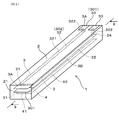
- FIG. 2 is a perspective view of a particulate matter detection sensor element (PM sensor element) according to the first embodiment.
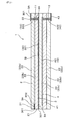
- FIG. 2 is an explanatory sectional view taken along line II-II in FIG. 1.
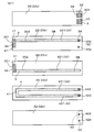
- FIG. 2 is an exploded plan view of the PM sensor element according to the first embodiment.
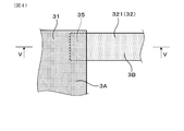
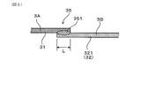
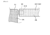
- FIG. 3 is an explanatory plan view of a connection portion between a detection electrode portion and a long wiring portion in the first embodiment.
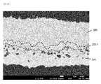
- FIG. 5 is a sectional view taken along line VV in FIG. 4. 4 is a cross-sectional photograph (approximately 5000 times) of an overlapping portion in the first embodiment.
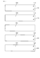
- FIG. 5 is an explanatory diagram of the method for manufacturing the PM sensor element according to the first embodiment, and is a plan view of a plurality of green sheets.
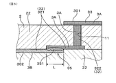
- FIG. 10 is a cross-sectional explanatory view of a base end portion of a long wiring portion, a conductor in a via, and a terminal portion according to the second embodiment.
- FIG. 13 is an exploded plan view of a PM sensor element according to the third embodiment.
- FIG. 10 is a plan view illustrating a connection portion between a detection electrode portion and a long wiring portion in a modified embodiment.
- the noble metal conductor has, as a main component, at least one or more noble metals selected from Pt (platinum), Au (gold), Pd (palladium), Rh (rhodium), and Ir (iridium).
- “having at least one or more noble metals selected from Pt, Au, Pd, Rh, and Ir as main components” means that the total mass of Pt, Au, Pd, Rh, and Ir is the total of the noble metal conductors. It means that it is 50% or more based on the mass.
- the noble metal conductor may include only one of Pt, Au, Pd, Rh, and Ir, or may include a plurality of types. Further, the noble metal conductor may include a ceramic such as alumina. However, the noble metal conductor may not include a ceramic such as alumina. When the noble metal conductor contains ceramic, its content is preferably, for example, 20% by weight or less.
- the low expansion conductor is mainly composed of a low expansion coefficient metal having a smaller linear expansion coefficient than a noble metal.
- “having a low expansion coefficient metal as a main component” means that the total mass of the low expansion metal is 50% or more of the total mass of the low expansion conductor.
- the low expansion coefficient metal is preferably at least one metal selected from W and Mo. This is because W and Mo are metals having a sufficiently smaller linear expansion coefficient than the noble metal. In addition, since W and Mo have a higher melting point than the noble metal conductor, not only the temperature cycle resistance but also the heat resistance and the strength can be improved in the detection conductor.
- the low expansion conductor may include only one of W and Mo, or may include both.
- the low expansion conductor may include a ceramic such as alumina. However, the low expansion conductor may not include a ceramic such as alumina. When the low expansion conductor contains ceramic, the content thereof is preferably, for example, 20% by weight or less.
- non-noble metal refers to Pt, Au, Pd, Rh, and Ir.
- the low expansion coefficient metal has a smaller linear expansion coefficient than the above-mentioned noble metals (that is, Pt, Au, Pd, Rh, and Ir).
- the linear expansion coefficient is JIS A value measured at a temperature of 20 ° C. in accordance with Z 2285 (2003, a method for measuring the coefficient of linear expansion of a metal material).
- the linear expansion coefficient of each metal, W: 4.5 ⁇ 10 -6 /K,Mo:4.0 ⁇ 10 -6 /K,Pt:8.8 ⁇ 10 -6 / K, Au: 14.2 is a ⁇ 10 -6 /K,Pd:11.8 ⁇ 10 -6 /K,Rh:8.2 ⁇ 10 -6 /K,Ir:6.2 ⁇ 10 -6 / K.
- the terminal portion be formed of the noble metal conductor.
- the oxidation resistance of the terminal portion can be improved. Since the terminal portion is also a portion exposed on the element surface, by configuring this portion with a noble metal conductor, the oxidation resistance of the detection conductor can be further improved.
- the PM sensor element performs sensing at a position closer to the center of the exhaust pipe than other sensor elements such as a gas sensor. Accordingly, not only the detection electrode part but also the terminal part of the PM sensor element are easily exposed to high temperatures. Therefore, in the PM sensor element, particularly, not only the detection electrode portion but also the terminal portion are required to have sufficient heat resistance and oxidation resistance. Therefore, by forming the terminal portion from a noble metal conductor as described above, its heat resistance and oxidation resistance can be improved, and it can meet the demands of the market.
- the low expansion conductor may be formed inside the insulating base.
- compatibility between the temperature cycle resistance and the oxidation resistance can be more effectively obtained. That is, since the low-expansion conductor is arranged inside the insulating base, the low-expansion conductor is less likely to be exposed to the gas containing oxygen, and the oxidation resistance of the detection conductor is easily improved.
- the temperature of the inside of the insulating base tends to rise when heated by the heater. Therefore, by using the low expansion conductor as a portion of the detection conductor formed inside the insulating base, the temperature cycle resistance can be effectively improved.
- the detection electrode portion may be formed between the plurality of insulating layers, and the detection surface may be formed on an end surface in a direction orthogonal to a laminating direction of the plurality of insulating layers. .
- the oxidation resistance of the detection conductor can be further improved. That is, when the detection electrode unit is formed between the plurality of insulating layers, the detection electrode unit is in a state of being sandwiched from the stacking direction. Therefore, when the insulating layer is fired, the detection electrode portion is compressed in the stacking direction. As a result, fine pores between the particles of the detection electrode portion are more likely to be smaller, and the intrusion of gas is more easily prevented. Therefore, the low expansion conductor in the insulating base is protected. Therefore, the oxidation resistance of the detection conductor can be improved.
- the detection conductor has an inner conductor formed between a plurality of the insulating layers, and an outer conductor formed on an outer surface of the insulating base in a laminating direction, and the inner conductor and the outer conductor Are provided between the inner and outer interlayer vias, and the conductors in the vias in the inner and outer interlayer vias may be the above-mentioned noble metal conductors.
- the outer layer conductor and the via conductor can both be formed of a noble metal conductor, the connection reliability between the two can be improved.
- the part of the inner layer conductor that is directly connected to the inner and outer interlayer vias connected to the outer layer conductor may be the noble metal conductor.
- the connection between the via conductor and the inner layer conductor is made to be a connection between the noble metal conductors, so that the connection reliability between the two can be improved.
- the overlapping portion has a solid solution layer of the noble metal and the low expansion coefficient metal.
- the stress at the joint interface between the noble metal conductor and the low expansion conductor can be further alleviated, and the connection reliability can be improved.
- the terminal portion is formed of the porous noble metal conductor.
- the contact resistance between the terminal portion and the external electrode can be reduced, and the electrical connection reliability can be improved.
- stress between the insulating substrate and the insulating base can be reduced.
- the adhesiveness of the terminal portion from the insulating base can be further improved.
- the detection conductor at least a part of a portion between the connection portion and the terminal portion configured by the low expansion conductor is configured by the noble metal conductor having a closed pore. Is preferred. In this case, it is possible to alleviate the stress between the conductor and the insulating base while preventing the gas from entering the low expansion conductor.
- having closed pores means a state in which pores are included in the noble metal conductor, and the pores are not communicated with the insulating base.
- the PM sensor element 1 of the present embodiment is an element that detects particulate matter in a gas to be measured.
- the PM sensor element 1 includes an insulating base 2, a detection conductor 3 formed on the insulating base 2, and a heater unit 4 formed on the insulating base 2.
- the PM sensor element 1 has a plurality of detection conductors 3 having different polarities from each other.
- the insulating base 2 has a detection surface 21 to which the particulate matter adheres.
- the detection conductor 3 has a detection electrode part 31, a terminal part 33, and a connection part 32. At least a part of the detection electrode unit 31 is exposed on the detection surface 21.
- the terminal section 33 is electrically connected to the detection electrode section 31 and is formed on the outer surface of the insulating base 2.
- the connection part 32 electrically connects the detection electrode part 31 and the terminal part 33.
- a portion of the detection conductor 3 including the detection electrode portion 31 is formed of a noble metal conductor 3A mainly containing at least one noble metal selected from Pt, Au, Pd, Rh, and Ir.
- a part of the connection portion 32 of the detection conductor 3 is formed of a low expansion conductor 3B mainly composed of a low expansion coefficient metal having a smaller linear expansion coefficient than a noble metal.
- the low expansion coefficient metal is made of at least one selected from W and Mo.
- the noble metal conductor 3A and the low expansion conductor 3B are overlapped with each other on the insulating layer 22 constituting the insulating base 2 in the normal direction of the insulating layer 22 to partially overlap each other.
- the detection conductor 3 has an exposed conductor portion 301 exposed on the element surface and a non-exposed conductor portion 302 not exposed on the element surface.
- the low expansion conductor 3 ⁇ / b> B is formed inside the insulating base 2. That is, the low expansion conductor 3B forms at least a part of the non-exposed conductor portion 302.
- the terminal portion 33 of the detection conductor 3 is also formed of the noble metal conductor 3A.
- the detection electrode section 31 and the terminal section 33 are made of the noble metal conductor 3A.
- the connection part 32 has the low expansion conductor 3B.
- the entire terminal portion 33 is also the exposed conductor portion 301, and is entirely made of the noble metal conductor 3A.
- a portion exposed on the detection surface 21 becomes an exposed conductor portion 301, and the other portion becomes a non-exposed conductor portion 302.
- the entirety of the detection electrode portion 31 including the non-exposed conductor portion 302 is made of the noble metal conductor 3A.
- the entirety of the connecting portion 32 is not made of the low expansion conductor 3B, but a part of the connecting portion 32 is made of the noble metal conductor 3A. Details of this point will be described later.
- the insulating base 2 has a long shape, and the connecting portion 32 has a long wiring portion 321 formed along the longitudinal direction of the insulating base 2.
- the long wiring portion 321 is made of the low expansion conductor 3B.
- the PM sensor element 1 of the present embodiment has a long, substantially rectangular parallelepiped shape.
- the insulating base 2 can be made of, for example, a ceramic containing alumina (Al 2 O 3 ) as a main component.
- the outer shape of the insulating base 2 has a substantially rectangular parallelepiped shape.
- the insulating base 2 is formed by laminating a plurality of insulating layers 22.
- the detection electrode unit 31 is formed between the plurality of insulating layers 22.
- the detection surface 21 is formed on an end surface in a direction orthogonal to the direction in which the plurality of insulating layers 22 are stacked. In the present embodiment, a detection surface 21 is provided on a surface on one end side in the longitudinal direction of the insulating base 2.
- FIG. 3 is an explanatory plan view showing a disassembled PM sensor element 1 between the insulating layers 22 as viewed from the laminating direction. Further, of the outer surfaces of the insulating base 2, a plane facing the laminating direction is the widest plane, and this plane is appropriately referred to as a main surface.
- a terminal portion 33 is formed at the base end of the insulating base 2.
- the terminal portion 33 is formed at the base end of the main surface of the insulating base 2.
- the connection part 32 is formed so that the detection electrode part 31 and the terminal part 33 which were each arrange
- a part of the connecting portion 32 is an inner conductor formed between the plurality of insulating layers 22.
- the PM sensor element 1 has an inner conductor as a non-exposed conductor portion 302.
- the detection conductor 3 has, as an exposed conductor portion 301, an outer layer conductor formed on the outer surface of the insulating base 2 in the laminating direction.
- An inner / outer interlayer via 11 is provided for interlayer connection between the inner conductor and the outer conductor.
- the in-via conductor 322 in the inner / outer interlayer via 11 is a noble metal conductor 3A.
- the connecting portion 32 includes the long wiring portion 321 and the via conductor 322. Further, the long wiring portion 321 is a part of the inner layer conductor.
- the inner layer conductor has a long wiring portion 321 and a detection electrode portion 31 connected to a tip portion thereof.
- the in-via conductor 322 that is a part of the connection portion 32 is made of the noble metal conductor 3A.
- the long wiring portion 321 other than the conductor 322 in the connecting portion 32 is formed of the low expansion conductor 3B.
- connection between the detection electrode section 31 and the long wiring section 321 is a connection between the noble metal conductor 3A and the low expansion conductor 3B.
- the noble metal conductor 3A and the low-expansion conductor 3B are located between the insulating layers 22 adjacent to each other in the laminating direction in the overlapping portion 35 partially overlapping each other in the thickness direction of the insulating layer 22.
- the length L of the overlapping portion 35 in the longitudinal direction of the long wiring portion 321 can be, for example, about 1 to 120 times the thickness of the noble metal conductor 3A.
- the overlapping portion 35 has a solid solution layer 351 of a noble metal and a low expansion metal.
- FIG. 6 shows a cross-sectional photograph of the overlapping portion 35. It can be confirmed that the solid solution layer 351 is formed between the noble metal Pt and the low expansion coefficient metal W. Note that the broken line shown in the photograph is an outline of the region where the solid solution layer 351 exists, which is assigned by the applicant.
- the PM sensor element 1 has a built-in heater unit 4. That is, the heater section 4 is formed inside the insulating base 2. The heater section 4 is formed at the interface between the plurality of insulating layers 22. The heater section 4 can also be constituted by the low expansion conductor 3B described above. Further, the heater section 4 has a heat generating section 41 and a pair of lead sections 42 connected to the heat generating section 41.
- Each lead 42 is connected to a pair of heater terminals 43 exposed on the element surface.
- the lead portion 42 has a long wiring portion 421 that is an inner layer conductor, and a via conductor 422 that connects the long wiring portion 421 and the heater terminal portion 43.
- the pair of heater terminal portions 43 are formed on the main surface of the insulating base 2 opposite to the side on which the terminal portions 33 of the detection conductor 3 are arranged. Further, the heater terminal section 43 is disposed at the base end of the insulating base 2, and the heat generating section 41 is disposed near the front end of the insulating base 2.
- the heating section 41 When the heater section 4 is energized, the heating section 41 generates heat, and the PM sensor element 1 is heated.
- the PM sensor element 1 can be used, for example, by being installed in an exhaust system of an internal combustion engine. Then, the amount of PM in the exhaust gas can be detected.
- the heater unit 4 When detecting PM, the heater unit 4 is energized to heat the PM sensor element 1 to, for example, about 600 to 800 ° C., as described above.
- a predetermined voltage is applied between the plurality of detection conductors 3 having different polarities. That is, a predetermined voltage is applied between the pair of terminal portions 33.
- the PM amount can be detected based on a change in the resistance value between the plurality of detection electrode portions 31 exposed on the detection surface 21.
- the PM sensor element 1 can be manufactured by performing the following green sheet forming step, through hole forming step, pattern printing step, degreasing / firing step, outer shape processing step, and pad forming step.
- the insulating base 2 can be obtained using a ceramic green sheet (hereinafter, appropriately referred to as a “green sheet”) formed by molding a raw material composition including a ceramic material, a binder resin, and the like.
- a ceramic green sheet hereinafter, appropriately referred to as a “green sheet” formed by molding a raw material composition including a ceramic material, a binder resin, and the like.
- Examples of the ceramic material include oxide ceramics, nitride ceramics, and carbide ceramics.
- Examples of the nitride ceramic include, for example, aluminum nitride, silicon nitride, boron nitride, and titanium nitride.
- Examples of the carbide ceramic include silicon carbide, zirconium carbide, titanium carbide, tantalum carbide, and tungsten carbide.
- Examples of the oxide ceramic include alumina, zirconia, cordierite, and mullite. Among these, it is preferable to use a ceramic containing alumina.
- an acrylic resin, an epoxy resin, or the like can be used as the binder resin.
- a solvent can be used to adjust the viscosity, and acetone, ethanol, and the like can be used as the solvent.
- a sintering aid can be added. Inorganic oxides such as SiO 2 , MgO, and CaO can be used as the sintering aid.
- a green sheet forming material is obtained by mixing a ceramic material, a binder resin, and the like, which are raw material compositions of the green sheet.
- a paste containing 70 to 95% by weight of Al 2 O 3 particles and further containing a binder resin and a solvent can be used.
- a green sheet is obtained by forming the green sheet forming material into a predetermined shape by screen printing, a doctor blade method, or the like, and drying the green sheet. A plurality of green sheets having substantially the same shape are obtained.
- FIG. 7 As shown in FIG. 7, among the green sheets 22a to 22e obtained by the green sheet forming step, through holes 110 and 120 penetrating in the thickness direction are formed in the green sheets 22a, 22b, 22d and 22e.
- the through holes 110 and 120 become the inner and outer interlayer vias 11 and 12 in the insulating base 2.
- the formation of the through holes 110 and 120 can be performed by punching, drilling, laser or the like. From the viewpoint of the accuracy of the inner diameter of the through hole, the formation of the through holes 110 and 120 is preferably performed by punching.
- a wiring pattern to be the detection conductor 3 or the heater unit 4 is formed by printing using a conductive paste on the green sheets 22a to 22e having the through holes 110 and 120 formed in the through hole forming step.
- the conductive paste used for pattern printing be made of metal particles, ceramic powder, binder resin, or the like.
- the binder resin include an acrylic resin and an epoxy resin.
- the solvent include acetone, ethanol, and the like.
- the average particle size of the metal particles contained in the conductive paste is preferably 0.1 to 10 ⁇ m.
- the average particle size of the metal particles is preferably 0.1 ⁇ m or more from the viewpoint of the ease of forming the wiring pattern, and 10 ⁇ m from the viewpoint of the ease of forming the wiring pattern and suppressing the variation in the electrical resistance of the wiring pattern. It is preferable to set the following.
- the ceramic powder for example, it is preferable to use alumina powder.
- the average particle size of the alumina powder may be, for example, about 0.1 to 10 ⁇ m, and the content thereof may be about 1 to 15 wt%.
- the conductive paste used in the pattern printing process is classified into a conductive paste for the noble metal conductor 3A, a conductive paste for the low expansion conductor 3B, and a conductive paste for the heater unit 4.
- a conductive paste for the noble metal conductor 3A a noble metal mainly selected from Pt, Au, Pd, Rh, and Ir can be used.
- a metal mainly selected from W and Mo can be used as the metal particles contained in the conductive paste for the low expansion conductor 3B.
- the metal particles contained in the conductive paste for the heater section 4 a metal selected from W and Mo can be used.
- the conductive paste for the low expansion conductor 3B of the detection conductor 3 and the conductive paste for the heater unit 4 may have the same composition.
- a mask having a screen mesh and having holes of a predetermined wiring pattern is used.
- a mask is set, and a wiring pattern is printed on the green sheets 22a to 22e using a squeegee (see FIG. 3).
- the printed conductive paste layer preferably has a thickness of 10 to 100 ⁇ m.
- the thickness of the conductive paste layer is preferably 10 ⁇ m or more from the viewpoint of ease of detection, and is preferably 100 ⁇ m or less from the viewpoint of ease of lamination.
- the pattern of the terminal portion 33 of the detection conductor 3 is printed on the green sheet 22a. This pattern printing is performed using a conductive paste for the noble metal conductor 3A. On the green sheets 22b and 22c, pattern printing of the inner layer conductor of the detection conductor 3 is performed. That is, the pattern of the detection electrode portion 31 and the pattern of the long wiring portion 321 of the connecting portion 32 are printed on the green sheets 22b and 22c.
- the pattern printing of the inner layer conductor of the detection conductor 3 is performed, for example, by first printing the detection electrode portion 31 with the conductive paste for the noble metal conductor 3A, and then printing the long length with the conductive paste for the low expansion conductor 3B.
- the wiring unit 321 is printed.
- the long wiring portion 321 may be printed with the conductive paste for the low expansion conductor 3B, and then the detection electrode portion 31 may be printed with the conductive paste for the noble metal conductor 3A.
- printing is performed so that the detection electrode unit 31 and the long wiring unit 321 form an overlapping portion 35 (see FIGS. 4 and 5) where the overlapping portion 35 partially overlaps.
- the pattern of the heater section 4 is printed on the green sheet 22d. As described above, this pattern printing can use the same conductive paste as the conductive paste for the low expansion conductor 3B.
- the pattern of the heater terminal 43 is printed on the green sheet 22e. This pattern printing can use the same thing as the conductive paste for the noble metal conductor 3A.
- the conductors are also filled in the through holes 110 and 120 in each of the green sheets 22a, 22b, 22d and 22e. That is, the conductor to be the conductor 322 in the via is filled in the through hole 110 of the green sheets 22a and 22b, and the conductor to be the conductor 422 in the via is filled in the through hole 120 of the green sheets 22d and 22e.
- a conductive paste for the noble metal conductor 3A can be used.
- the conductors in the through holes 110 and 120 may be formed at the same time by filling the insides of the through holes 110 and 120 with a conductive paste at the time of printing the wiring pattern on the surface of each of the green sheets 22a to 22e. It may be performed separately from printing. As described above, as shown in FIG. 3, the conductor pattern is printed on each of the green sheets 22a to 22e.
- the conductive paste formed on the green sheets 22a to 22e is dried by drying the pattern-printed green sheets 22a to 22e. Drying can be performed, for example, at 40 to 130 ° C. for 1 to 60 minutes.
- the green sheets 22a to 22e (see FIG. 3) on which the pattern is formed in the pattern printing step are appropriately laminated. Thereby, a laminate of the green sheets 22a to 22e on which the conductive paste is formed is obtained.
- the laminate obtained in the laminating step is degreased and fired.
- the degreasing step can be performed, for example, at 80 to 800 ° C. for 1 to 30 hours in an N 2 -containing atmosphere or a humidified H 2 O / H 2 atmosphere.
- the firing step is preferably performed, for example, at 1000 to 1600 ° C. for 1 to 40 hours in an inert atmosphere.
- the degreasing / firing step is preferably performed in a state where the laminate is pressed in the lamination direction in order to improve the adhesion between the insulating layers 22.
- Pad forming step A conductive paste such as Pt mixed with borosilicate glass is printed on the heater terminal 43 exposed from the insulating base 2 in order to prevent the heater terminal 43 from deteriorating. Thereafter, baking is performed at 800 to 1000 ° C.
- a portion including the detection electrode portion 31 in the detection conductor 3 is formed of the noble metal conductor 3A. That is, the portion of the detection conductor 3 exposed to the gas to be measured is formed of the noble metal conductor 3A. Therefore, the oxidation resistance of the detection conductor 3 can be improved.
- the connecting portion 32 is formed of the low-expansion conductor 3B whose main component is a low-expansion metal having a lower linear expansion coefficient than the noble metal.
- the connecting portion 32 is exposed to the temperature cycle, the influence of the stress generated by expansion and contraction thereof can be suppressed. That is, the connection portion 32 formed over a relatively wide range is likely to be subjected to stress due to expansion during heating by the heater portion. Therefore, by making at least a part of the connecting portion 32 of the detection conductor 3 a low expansion conductor 3B having a small linear expansion coefficient, the temperature cycle resistance can be effectively improved.
- the noble metal conductor 3 ⁇ / b> A and the low expansion conductor 3 ⁇ / b> B are joined on the insulating layer 22 forming the insulating base 2 by overlapping portions 35 partially overlapping each other in the normal direction of the insulating layer 22.
- the connection reliability of the joint between the noble metal conductor 3A and the low expansion conductor 3B can be improved. That is, by providing the overlapping portion 35, it is easy to secure a connection area between the noble metal conductor 3A and the low expansion conductor 3B, and it is easy to suppress stress concentration at the joint. As a result, the connection reliability of the joint between the noble metal conductor 3A and the low expansion conductor 3B can be improved.
- the detection conductor 3 as described above, it is possible to achieve both the temperature cycle resistance and the oxidation resistance of the detection conductor 3.
- the terminal portion 33 of the detection conductor 3 is formed of the noble metal conductor 3A.
- the oxidation resistance of the terminal portion 33 can be improved. Since the terminal portion 33 is also the exposed conductor portion 301, the oxidation resistance of the detection conductor 3 can be further improved by configuring this portion with the noble metal conductor 3A.
- the low expansion conductor 3B is formed inside the insulating base 2. This makes it possible to more effectively achieve both the temperature cycle resistance and the oxidation resistance. That is, since the low-expansion conductor 3B is arranged inside the insulating base 2, the low-expansion conductor 3B is less likely to be exposed to a gas containing oxygen, and the oxidation resistance of the detection conductor 3 is easily improved. On the other hand, the temperature of the inside of the insulating base 2 tends to rise when heated by the heater unit 4. Therefore, by making the low expansion conductor 3B a part of the detection conductor 3 formed inside the insulating base 2, the temperature cycle resistance can be effectively improved.
- the detection electrode portion 31 is formed between the plurality of insulating layers 22, and the detection surface 21 is formed on an end surface of the plurality of insulating layers 22 in a direction orthogonal to the laminating direction. Thereby, the oxidation resistance of the detection conductor 3 can be further improved. That is, when the detection electrode unit 31 is formed between the plurality of insulating layers 22, the detection electrode unit 31 is in a state of being sandwiched from the stacking direction. Therefore, when the insulating layer 22 is fired, the detection electrode unit 31 is compressed in the stacking direction. As a result, fine pores between particles in the detection electrode unit 31 are more likely to be smaller, and gas intrusion is more easily prevented. Therefore, the low expansion conductor 3B in the insulating base 2 is protected. Therefore, the oxidation resistance of the detection conductor 3 can be improved.
- the via conductor 322 is the noble metal conductor 3A.
- the connection reliability between the outer conductor and the via conductor 322 can be improved. That is, although the via conductor 322 is covered with the outer conductor (the terminal portion 33 in the present embodiment) and becomes the non-exposed conductor portion 302, gas may enter through the fine pores in the outer conductor. . It is conceivable that this gas reaches the interface between the outer conductor and the via conductor 322. Therefore, by forming the via conductor 322 with the noble metal conductor 3A, the oxidation resistance can be improved and the connection reliability can be improved. In particular, by configuring the terminal portion 33 and the via conductor 322 with the same type of noble metal conductor 3A, the connection reliability between them can be further improved.
- the overlapping portion 35 has a solid solution layer 351 of a noble metal and a low expansion coefficient metal.
- the noble metal conductor 3A From the viewpoint of oxidation resistance, it is particularly preferable to use at least one noble metal selected from Pt, Rh, and Ir as the noble metal conductor 3A. Further, from the viewpoint of further improving the oxidation resistance and the temperature cycle resistance, it is particularly preferable to use the noble metal conductor 3A mainly containing Pt and the low expansion conductor 3B mainly containing W.
- the present embodiment is a form of the PM sensor element 1 in which a portion of the inner layer conductor directly connected to the inner and outer interlayer vias 11 connected to the outer layer conductor is made of the noble metal conductor 3A. .
- a part of the base wiring side of the long wiring portion 321 as the inner layer conductor is formed of the noble metal conductor 3A.
- the in-via conductor 322 is connected to a portion of the long wiring portion 321 constituted by the noble metal conductor 3A.
- the via conductor 322 is made of the noble metal conductor 3A, as in the first embodiment.
- the via conductor 322 and the noble metal conductor 3A in the long wiring portion 321 are made of the same kind of noble metal.
- connection between the noble metal conductor 3A and the low expansion conductor 3B in the long wiring portion 321 is formed by the overlapping portion 35. That is, the noble metal conductor 3A at the base end of the long wiring portion 321 and the low-expansion conductor 3B at the tip end thereof form an overlapping portion 35 that partially overlaps in the laminating direction.
- the overlapping portion 35 can be the same as the overlapping portion 35 between the tip of the long wiring portion 321 and the detection electrode portion 31 in the first embodiment.
- the length L of the overlapping portion 35 in the long wiring portion 321 is twice or more the thickness of the noble metal conductor 3A.
- the length L of the overlapping portion 35 is preferably equal to or larger than the inner diameter of the inner / outer interlayer via 11.
- the inner and outer interlayer vias 11 and the overlapping portion 35 do not overlap in the stacking direction.
- the connection reliability between the via conductor 322 and the inner layer conductor can be improved.
- the joint area between the via conductor 322 formed of the noble metal conductor 3A and the inner layer conductor (the long wiring portion 321) is equal to or less than the opening area of the inner and outer interlayer via 11, and depending on the size of the inner and outer interlayer via 11 The area is limited. Therefore, if the joint between the via conductor 322 and the long wiring portion 321 is a joint between the noble metal conductor 3A and the low expansion conductor 3B, there is a possibility that the joining reliability may be disadvantageous. Therefore, by making this connection the connection between the noble metal conductors 3A, the connection reliability of the detection conductor 3 can be improved.
- the third embodiment has the same functions and effects as the first embodiment.
- FIG. 9 is an exploded explanatory view in which the PM sensor element 1 is disassembled at the interface of the insulating layer 22.
- Reference numerals 22a, 22b, 22d, and 22e shown in FIG. 4 roughly correspond to the green sheets 22a, 22b, 22d, and 22e in the manufacturing method described in the first embodiment.
- the pattern of the detection conductor 3 formed on the green sheets 22a and 22b is different from that of the first embodiment.
- the detection electrode portion 31 of the detection conductor 3 is provided on the main surface of the insulating base 2. Two detection electrode portions 31 having different polarities are formed adjacent to each other on the same main surface of the insulating base 2 while providing a predetermined interval.
- Each detection conductor 3 is formed in a substantially comb-teeth shape. That is, each detection electrode section 31 has a base 311 extending in the longitudinal direction of the insulating base 2 and a plurality of branch sections 312 branched from the base 311 and protruding inward. The branch portions 312 of one detection electrode portion 31 and the branch portions 312 of the other detection electrode portion 31 are alternately arranged in the longitudinal direction of the insulating base 2 while providing a predetermined interval.
- the terminal portion 33 of each detection conductor 3 is formed at the base end of the main surface of the insulating base 2 as in the first embodiment.
- the detection electrode section 31 and the terminal section 33 are provided on the same main surface of the insulating base 2.
- the connecting portion 32 connecting the detection electrode portion 31 and the terminal portion 33 is mainly buried inside the insulating base 2.
- both of the long wiring portions 321 of the pair of connecting portions 32 are formed of the insulating layer 22 on which the detection electrode portion 31 and the terminal portion 33 are formed and the insulating layer 22 laminated on the inner surface thereof. It is formed between them.
- the pair of long wiring portions 321 are connected to the pair of detection electrode portions 31 via the via conductors 322 at the respective distal ends. Further, the pair of long wiring portions 321 are respectively connected to the pair of terminal portions 33 via the via conductors 322 at the respective base end portions.
- the entirety of the detection electrode portion 31 and the entirety of the terminal portion 33 become the exposed conductor portion 301.
- the connecting portion 32 becomes the non-exposed conductor portion 302.
- the detection electrode part 31 and the terminal part 33 consist of a noble metal conductor 3A.
- the via conductor 322 is made of the noble metal conductor 3A.
- the long wiring portion 321 of the connecting portion 32 is made of the low expansion conductor 3B except for both end portions.
- both ends of the long wiring portion 321 are formed of the noble metal conductor 3A.
- the overlapping portion 35 is formed at the joint between the low expansion conductor 3B and the noble metal conductor 3A in the long wiring portion 321.
- the present embodiment is a form of the PM sensor element 1 in which the terminal portion 33 is formed of a porous noble metal conductor 3A and the via conductor 322 is formed of a noble metal conductor 3A having closed pores. That is, the terminal portion 33 is formed of the porous noble metal conductor 3A, and at least a part of the portion of the detection conductor 3 between the connecting portion 32 formed of the low expansion conductor 3B and the terminal portion 33. Is composed of a noble metal conductor 3A having closed pores.
- the noble metal conductor 3A has a large number of pores. Some of the pores are open on the surface.
- the noble metal conductor 3A has closed pores, that is, isolated pores that do not communicate with the outside.
- the via conductor 322 is in a state where no ventilation path is formed between both open ends of the inner and outer interlayer vias 11.
- the heater terminal portion 43 is formed of a porous noble metal conductor, similarly to the terminal portion 33, and the via conductor 422 is formed of a noble metal conductor having closed pores, similarly to the via conductor 322. ing.
- the detection electrode portion 31 is formed of a noble metal conductor 3A having closed pores, similarly to the conductor 322 in the via. Other configurations are the same as in the first embodiment.
- the conductive paste used for the terminal portion 33 and the heater terminal portion 43 is different from the conductive paste used for the detection electrode portion 31 and the like.
- the conductive paste used for the terminal portion 33 and the heater terminal portion 43 a material in which glass frit or the like is mixed in addition to metal particles and ceramic powder can be used.
- the formation of the terminal portion 33 and the heater terminal portion 43 is performed after the [degreasing / firing step]. That is, in the [pattern printing step] of the first embodiment, the terminal portion 33 and the heater terminal portion 43 have the same conductivity as the other detection conductors 3 (detection electrode portions 31 and the like) on the green sheet before firing. Although it has been described that the conductive paste is printed, in the present embodiment, the printing of the terminal portion 33 and the terminal portion 43 for the heater is performed after firing of the laminate.
- the pattern of the terminal portion 33 and the heater terminal portion 43 is printed on the fired laminate on which other portions of the conductor are formed.
- the porous terminal portions 33 and the heater terminal portions 43 are formed.
- the relative density of the fired terminal 33 and the heater terminal 43 is preferably 50 to 95%.
- the relative density is less than 50%, the strength of the terminal portion 33 and the terminal portion 43 for the heater (hereinafter, also appropriately referred to as the terminal portion 33 or the like) may be insufficient, and the electric resistance may be too large.
- the relative density is greater than 95%, it may be difficult to sufficiently obtain the effect of stress relaxation described below.
- the terminal portion 33 and the like are formed of the porous noble metal conductor 3A, the stress between the terminal portion 33 and the insulating base 2 can be reduced. As a result, the adhesion of the terminal portion 33 and the like to the insulating base 2 can be improved.
- the terminal portion 33 and the like are made porous, there is a concern that gas (air or the like) from the outside may permeate the terminal portion 33 and enter the connecting portion 32.
- gas air or the like
- the low-expansion conductor 3B in the connecting portion 32 there is a concern that oxidation may occur.
- the in-via conductors 322 and 422 are formed of the noble metal conductor 3A having closed pores, it is possible to prevent gas from entering the low expansion conductor 3B. Further, since the in-via conductors 322 and 422 are formed of the noble metal conductor 3A having closed pores, the stress of the in-via conductors 322 and 422 in the inner and outer interlayer vias 11 and 12 can be reduced. Therefore, the thermal cycling resistance can be further improved.
- the third embodiment has the same functions and effects as the first embodiment.
- the terminal portion 33 is formed by forming a portion of the base end side of the long wiring portion 321 as the connecting portion 32 with the noble metal conductor 3A. It is a porous form.
- At least one of the noble metal conductor 3A forming the via conductor 322 and the noble metal conductor 3A forming the base end of the long wiring portion 321 has closed pores.
- Both the noble metal conductor 3A forming the via conductor 322 and the noble metal conductor 3A forming the base end of the long wiring portion 321 may be the noble metal conductor 3A having closed pores.
- Other configurations are the same as those of the second embodiment.
- the porous noble metal conductor 3A and the noble metal conductor 3A having closed pores have the same configuration as that of the fourth embodiment, and can be formed by the same method as that of the fourth embodiment.
- At least one of the noble metal conductor 3A forming the via conductor 322 and the noble metal conductor 3A forming the base end of the long wiring portion 321 is the noble metal conductor 3A having closed pores. Therefore, even if the gas permeates the terminal portion 33, it is possible to prevent the gas from reaching at least the low expansion conductor 3B of the connecting portion 32.
- the third embodiment has the same functions and effects as those of the second and fourth embodiments.
- the sample 1 is the PM sensor element 1 of the first embodiment, and a specific manufacturing method thereof will be described together with specific materials, specific dimensions, and the like in the following ⁇ Sample 1>.
- the sample 2 is a PM sensor element in which the entirety of the detection conductor is made of the same material containing Pt as a main component. Others are the same as the sample 1.
- Sample 3 is a PM sensor element in which the entirety of the detection conductor is made of the same material containing W as a main component. Others are the same as the sample 1.
- the molding material was measured by a doctor blade method to have a size of length: 4 mm x width: 50 mm x thickness: 0.02 mm, and dried at 80 ° C for 60 minutes to form a green sheet. Note that a total of five green sheets 22a to 22e were prepared. Each of the green sheets 22a, 22b, 22d, and 22e was provided with through holes 110 and 120 (inner and outer interlayer vias 11 and 12) having a diameter of 6 mm by punching.
- conductive pastes A, B, and D using Pt particles and a conductive paste C using W particles were produced.
- the details of each conductive paste are shown below.
- Alumina powder (average particle diameter: 0.3 ⁇ m) 15 wt% 30 parts by weight of an acrylic resin as a binder and 10 parts by weight of terpineol as a solvent were mixed with 100 parts by weight of a mixed powder of Pt particles and alumina powder.
- the conductive paste A was filled into the through holes 110 of the green sheet 22b by printing. As a result, a part of the via conductor 322 was formed. Further, using a mask provided with a screen mesh on which the pattern of the long wiring portion 321 of the detection conductor 3 for the positive electrode is drawn, the long wiring portion is formed on the main surface of the green sheet 22b with the conductive paste C. 321 was printed. After that, using a mask provided with a screen mesh on which the pattern of the detection electrode portion 31 for the positive electrode was drawn, the detection electrode portion 31 for the positive electrode was printed on the main surface of the green sheet 22b with the conductive paste B. .
- the detection electrode portion 31 for the positive electrode has a length of 3 mm, a width of 0.6 mm, and a thickness of 0.03 mm, and the long wiring portion 321 has a line width of 0.4 mm and a thickness of 0.03 mm.
- the detection electrode portion 31 for the negative electrode has a length of 3 mm, a width of 0.6 mm and a thickness of 0.03 mm, and the long wiring portion 321 has a line width of 0.4 mm and a thickness of 0.03 mm.
- the conductive paste A was filled into the through holes 120 of the green sheet 22d by printing. Thereby, a part of the via conductor 422 was formed. After that, the heater 4 was printed on the main surface of the green sheet 22d with the conductive paste C using a mask provided with a screen mesh on which the pattern of the heater 4 was drawn.
- the heater section 4 had a width of 0.4 mm and a thickness of 0.03 mm.
- Green sheets 22a, 22b, 22c, 22d, and 22e were laminated in this order to obtain a laminate. It should be noted that only the green sheet 22e was laminated with the surface on which the conductive paste was printed facing the other green sheet 22a to 22d opposite to the other green sheets 22a to 22d.
- the laminate was degreased at 600 ° C. for 4 hours under a humidified H 2 O / H 2 atmosphere, and baked at 1400 ° C. for 5 hours under an inert atmosphere. Thus, a sintered body of the laminate was obtained.
- Terminal part forming step By grinding both main surfaces of the sintered body, the conductors 322 and 422 in the via were exposed. Then, the conductive paste D was printed on the surface of the sintered body where the conductor 422 in the via was exposed, and heated at 900 ° C. for 1 hour to form the heater terminal portion 43. Similarly, the conductive paste D was printed on the surface of the sintered body where the conductor 322 in the via was exposed, and heated at 900 ° C. for 1 hour to form the heater terminal portion 43. The printing of the conductive paste D was performed using a mask provided with a screen mesh on which a pattern of the heater terminal portion 43 or the terminal portion 33 was drawn.
- the heater terminal portion 43 was formed in two dimensions, one for the positive electrode and one for the negative electrode, with a size of 2 mm in length, 2 mm in width, and 0.03 mm in thickness.
- the terminal portion 33 was formed in two dimensions, one for the positive electrode and the other for the negative electrode, with a size of 2 mm in length ⁇ 2 mm in width ⁇ 0.03 mm in thickness.
- the PM sensor element 1 of the sample 1 was obtained.
- the PM sensor element 1 of the sample 1 was obtained.
- Temperature cycle evaluation The initial evaluation is performed by heating the PM sensor element between room temperature and 800 ° C., stopping the heating 3 minutes after reaching 800 ° C., and returning to room temperature. This cycle was repeated 100 times. After confirming that the PM sensor element after the temperature cycle was heated to 800 ° C., a predetermined voltage was applied at this temperature state for 100 hours. The PM sensor element to which the voltage application was completed was operated, and the operation state, current value, and appearance of the PM sensor were checked.
- two detection electrode units are shown. However, for example, three or more detection electrode units may be provided.
- the form in which the noble metal conductor 3 ⁇ / b> A was formed from above the low expansion conductor 3 ⁇ / b> B as the overlapping portion 35 was described, Is not particularly limited. That is, as shown in FIG. 10, for example, the low expansion conductor 3B may be overlaid on the noble metal conductor 3A to form an overlapping portion.
- a convex pattern 313 protruding toward the low expansion conductor 3B is formed on a part of the detection electrode portion 31 made of the noble metal conductor 3A so that a part thereof overlaps the convex pattern 313.
- a long wiring portion 321 made of the low expansion conductor 3B is formed.
- the low expansion conductor 3B is formed so as to press down three sides of the convex pattern 313.
- the present invention is not limited to the above embodiments, and can be applied to various embodiments without departing from the gist thereof.
Landscapes
- Chemical & Material Sciences (AREA)
- Analytical Chemistry (AREA)
- Physics & Mathematics (AREA)
- Health & Medical Sciences (AREA)
- Life Sciences & Earth Sciences (AREA)
- Biochemistry (AREA)
- General Health & Medical Sciences (AREA)
- General Physics & Mathematics (AREA)
- Immunology (AREA)
- Pathology (AREA)
- Dispersion Chemistry (AREA)
- Electrochemistry (AREA)
- Chemical Kinetics & Catalysis (AREA)
- Investigating Or Analyzing Materials By The Use Of Electric Means (AREA)
Abstract
耐温度サイクル性の向上と耐酸化性の向上との両立を図ることができる粒子状物質検出センサ素子を提供する。粒子状物質検出センサ素子は、検出面を有する絶縁基体と、絶縁基体に形成された複数の検出用導体と、絶縁基体に形成されたヒータ部と、を有する。検出用導体は、検出電極部(31)と端子部と連結部(32)とを有する。検出用導体のうち、検出電極部(31)を含む部位は、Pt、Au、Pd、Rh、Irから選ばれる少なくとも一種以上の貴金属を主成分とする貴金属導体(3A)にて構成されている。連結部(32)の少なくとも一部は、貴金属よりも線膨張係数が小さい低膨張率金属を主成分とする低膨張導体(3B)にて構成されている。貴金属導体(3A)と低膨張導体(3B)とは、絶縁基体を構成する絶縁層上において、絶縁層の法線方向に、部分的に互いに重なり合った重複部(35)によって接合されている。
Description
本発明は、被測定ガス中の粒子状物質を検出する粒子状物質検出センサ素子に関する。
例えば、内燃機関から排出される排ガス中の粒子状物質(すなわち、Particulate Matter:PM)の量を検出するために、電気抵抗式の粒子状物質検出センサ(以下において、適宜、PMセンサともいう)が使用されている。
特許文献1には、積層構造の絶縁性基体の表面に、粒子状物質を検出するための検出部を有する粒子状物質検出センサ素子(以下において、適宜、PMセンサ素子ともいう)が開示されている。検出部には、検出電極が露出している。また、引出電極が絶縁性基体に埋設されている。また、検出部を加熱するためのヒータが、絶縁性基体に埋設されている。
特許文献2には、白金を主原料とする検出電極と、モリブデン又はタングステンを主原料とする引き出し電極とを有するセンサ素子が開示されている。
しかしながら、PMセンサ素子には、耐久性の向上が求められている。具体的には、耐温度サイクル性、耐酸化性等の耐久性を向上させることが求められている。すなわち、PMセンサ素子は、ヒータ部によって、例えば600~800℃という高温に加熱された状態にて粒子状物質検出の測定を行なう。そのため、PMセンサ素子は、常温と、上記の高温との間の温度サイクルを繰り返すこととなる。
それゆえ、PMセンサ素子の検出用導体は、温度サイクルの影響を受けても、長期使用に対する耐久性を有することが必要である。その一方で、検出用導体は、高温下に晒されても、酸化の影響を受けないで、粒子状物質を検出する機能を維持することが必要である。
特許文献1に開示されたPMセンサ素子においては、基本的に同一材料にて、検出用導体の全体が形成されることとなる。そうすると、特許文献1に開示されたPMセンサ素子における検出用導体は、温度サイクルの影響による応力の低減(以下において、適宜「耐温度サイクル性の向上」という)と、耐酸化性の向上との両立は困難といえる。つまり、特許文献1に開示されたPMセンサ素子に温度サイクルを行なったとき、検出用導体の全体に、ある材料(例えばAu)を用いた場合は、温度サイクルによって発生する応力の影響を低減させ難く、他のある材料(例えばW)を用いた場合には、高温下に晒されたときの耐酸化性を確保し難くなる。
特許文献2に開示されたPMセンサ素子においては、検出電極と、引き出し電極とを、互いに異なる材料にて形成している。そして、引き出し電極をタングステン又はモリブデンにて構成している。ところが、異なる材料からなる部位同士の接合部分において、接続信頼性が懸念される。したがって、特許文献2に開示されたPMセンサ素子においても、耐温度サイクル性の向上と耐酸化性の向上との両立を図ることはできていない。
本発明は、かかる背景に鑑みてなされたものであり、耐温度サイクル性の向上と耐酸化性の向上との両立を図ることができる粒子状物質検出センサ素子を提供しようとするものである。
本発明の一態様は、被測定ガス中の粒子状物質を検出する粒子状物質検出センサ素子であって、
粒子状物質を付着させる検出面を有する絶縁基体と、
上記絶縁基体に形成された互いに極性の異なる複数の検出用導体と、
上記絶縁基体に形成されたヒータ部と、を有し、
上記検出用導体は、少なくとも一部が上記検出面に露出した検出電極部と、
上記検出電極部に電気的に接続されると共に、上記絶縁基体の外表面に形成された端子部と、
上記検出電極部と上記端子部とを電気的に接続する連結部と、を有し、
上記検出用導体のうち、少なくとも、上記検出電極部を含む部位は、Pt、Au、Pd、Rh、Irから選ばれる少なくとも一種以上の貴金属を主成分とする貴金属導体にて構成されており、
上記連結部の少なくとも一部は、上記貴金属よりも線膨張係数が小さい低膨張率金属を主成分とする低膨張導体にて構成されており、
上記貴金属導体と上記低膨張導体とは、上記絶縁基体を構成する絶縁層上において、該絶縁層の法線方向に、部分的に互いに重なり合った重複部によって接合されている、粒子状物質検出センサ素子にある。
粒子状物質を付着させる検出面を有する絶縁基体と、
上記絶縁基体に形成された互いに極性の異なる複数の検出用導体と、
上記絶縁基体に形成されたヒータ部と、を有し、
上記検出用導体は、少なくとも一部が上記検出面に露出した検出電極部と、
上記検出電極部に電気的に接続されると共に、上記絶縁基体の外表面に形成された端子部と、
上記検出電極部と上記端子部とを電気的に接続する連結部と、を有し、
上記検出用導体のうち、少なくとも、上記検出電極部を含む部位は、Pt、Au、Pd、Rh、Irから選ばれる少なくとも一種以上の貴金属を主成分とする貴金属導体にて構成されており、
上記連結部の少なくとも一部は、上記貴金属よりも線膨張係数が小さい低膨張率金属を主成分とする低膨張導体にて構成されており、
上記貴金属導体と上記低膨張導体とは、上記絶縁基体を構成する絶縁層上において、該絶縁層の法線方向に、部分的に互いに重なり合った重複部によって接合されている、粒子状物質検出センサ素子にある。
上記粒子状物質検出センサ素子においては、上記検出用導体のうち、上記検出電極部を含む部位が、上記貴金属導体にて構成されている。すなわち、検出用導体のうち、被測定ガスに曝される箇所は、貴金属導体にて構成されている。それゆえ、検出用導体の耐酸化性を向上させることができる。
上記連結部の少なくとも一部は、上記貴金属よりも線膨張係数が小さい低膨張率金属を主成分とする低膨張導体にて構成されている。これにより、連結部が、温度サイクルに曝されたとき、その膨脹、収縮により発生した応力の影響を抑制することができる。つまり、比較的広範囲にわたって形成される連結部は、ヒータ部による加熱時における膨張によって、応力が作用しやすい。そこで、検出用導体のうち、連結部の少なくとも一部を、線膨張係数の小さい低膨張導体とすることで、効果的に耐温度サイクル性を向上させることができる。
そして、貴金属導体と低膨張導体とは、上記絶縁基体を構成する絶縁層上において、該絶縁層の法線方向に、部分的に互いに重なり合った重複部によって接合されている。これにより、貴金属導体と低膨張導体との接合部の接続信頼性を向上させることができる。すなわち、重複部を設けることにより、貴金属導体と低膨張導体との接続面積を確保しやすく、また、接合部における応力集中を抑制しやすい。その結果、貴金属導体と低膨張導体との接合部の接続信頼性を向上させることができる。
このように、検出用導体の構成を上記のようにすることにより、検出用導体の耐温度サイクル性と耐酸化性との両立を図ることができる。
このように、検出用導体の構成を上記のようにすることにより、検出用導体の耐温度サイクル性と耐酸化性との両立を図ることができる。
以上のごとく、上記態様によれば、耐温度サイクル性の向上と耐酸化性の向上との両立を図ることができる粒子状物質検出センサ素子を提供することができる。
上記貴金属導体は、上述のように、Pt(白金)、Au(金)、Pd(パラジウム)、Rh(ロジウム)、Ir(イリジウム)から選ばれる少なくとも一種以上の貴金属を主成分とする。ここで、「Pt、Au、Pd、Rh、Irから選ばれる少なくとも一種以上の貴金属を主成分とする」とは、Pt、Au、Pd、Rh、Irの質量の合計が、貴金属導体の全体の質量に対して、50%以上であることを意味する。貴金属導体は、Pt、Au、Pd、Rh、Irのうちの一種のみを含んでいてもよいし、複数種類を含んでいてもよい。また、貴金属導体は、アルミナ等のセラミックが含まれているものとすることができる。ただし、貴金属導体は、アルミナ等のセラミックが含まれていないものとすることもできる。貴金属導体にセラミックが含まれる場合には、その含有量は、例えば、20重量%以下であることが好ましい
。
。
上記低膨張導体は、貴金属よりも線膨張係数が小さい低膨張率金属を主成分とする。ここで、「低膨張率金属を主成分とする」とは、低膨張率金属の質量の合計が、低膨張導体の全体の質量に対して、50%以上であることを意味する。
上記低膨張率金属は、W、Moから選ばれる少なくとも一種以上の金属であることが好ましい。W、Moは、貴金属よりも充分に線膨張係数が小さい金属であるからである。また、W、Moは、貴金属導体よりも高融点であるため、耐温度サイクル性だけでなく、耐熱性の向上、強度向上を、検出用導体にもたらすことができる。
低膨張導体は、W、Moのいずれか一方のみを含んでいてもよいし、双方を含んでいてもよい。また、低膨張導体は、アルミナ等のセラミックを含んでいるものとすることができる。ただし、低膨張導体は、アルミナ等のセラミックを含まないものとすることもできる。低膨張導体にセラミックが含まれる場合には、その含有量は、例えば、20重量%以下であることが好ましい
。
低膨張導体は、W、Moのいずれか一方のみを含んでいてもよいし、双方を含んでいてもよい。また、低膨張導体は、アルミナ等のセラミックを含んでいるものとすることができる。ただし、低膨張導体は、アルミナ等のセラミックを含まないものとすることもできる。低膨張導体にセラミックが含まれる場合には、その含有量は、例えば、20重量%以下であることが好ましい
。
なお、本明細書において、「貴金属」というときは、Pt、Au、Pd、Rh、Irのことをいう。そして、低膨張率金属は、上記の貴金属(すなわち、Pt、Au、Pd、Rh、Ir)よりも線膨張係数が小さい。
また、線膨張係数は、JIS
Z 2285(2003 金属材料の線膨張係数の測定方法)に準拠して、温度20℃にて測定を行なった値とする。その一例として、各金属の線膨張係数は、W:4.5×10⁻⁶/K、Mo:4.0×10-6/K、Pt:8.8×10-6/K、Au:14.2×10-6/K、Pd:11.8×10-6/K、Rh:8.2×10-6/K、Ir:6.2×10-6/Kである。
また、線膨張係数は、JIS
Z 2285(2003 金属材料の線膨張係数の測定方法)に準拠して、温度20℃にて測定を行なった値とする。その一例として、各金属の線膨張係数は、W:4.5×10⁻⁶/K、Mo:4.0×10-6/K、Pt:8.8×10-6/K、Au:14.2×10-6/K、Pd:11.8×10-6/K、Rh:8.2×10-6/K、Ir:6.2×10-6/Kである。
また、上記検出用導体のうち、上記端子部は、上記貴金属導体にて構成されていることが好ましい。この場合には、端子部の耐酸化性を向上させることができる。端子部も、素子表面に露出する部分であるため、この部位を貴金属導体にて構成することで、検出用導体の耐酸化性を一層向上させることができる。また、PMセンサ素子は、例えばガスセンサ等、他のセンサ素子に比べて、排気管のより中央に近い位置においてセンシングを行うことが望まれる。それに伴い、PMセンサ素子は、検出電極部のみならず、端子部も、高温にさらされやすくなる。それゆえ、PMセンサ素子においては、特に、検出電極部のみならず、端子部にも、充分な耐熱性、耐酸化性が求められやすい。そこで、上記のように端子部も貴金属導体にて構成することによって、その耐熱性、耐酸化性を向上させ、市場の要求に応えることができる。
また、上記低膨張導体は、上記絶縁基体の内部に形成されているものとすることができる。この場合には、耐温度サイクル性と耐酸化性との両立を、より効果的に得ることができる。つまり、低膨張導体が絶縁基体の内部に配置されていることで、低膨張導体が酸素を含むガスに曝され難くなり、検出用導体の耐酸化性を向上させやすい。その一方で、絶縁基体の内部は、ヒータ部による加熱時において、温度上昇しやすい。そこで、低膨張導体が、検出用導体のうち絶縁基体の内部に形成された部位とすることで、効果的に耐温度サイクル性を向上させることができる。
また、検出電極部は、複数の上記絶縁層の間に形成されており、上記検出面は、複数の上記絶縁層の積層方向に直交する方向の端面に形成されているものとすることができる。この場合には、検出用導体の耐酸化性を一層向上させることができる。すなわち、検出電極部が複数の絶縁層の間に形成されている場合、検出電極部が積層方向から挟持された状態にある。それゆえ、絶縁層の焼成時において、検出電極部が積層方向に圧縮される。その結果、検出電極部の粒子間の微細な気孔がより小さくなりやすく、ガスの侵入をより阻止しやすくなる。それゆえ、絶縁基体内の低膨張導体を保護することとなる。したがって、検出用導体の耐酸化性を向上させることができる。
また、上記検出用導体は、複数の上記絶縁層の間に形成された内層導体と、積層方向における上記絶縁基体の外表面に形成された外層導体とを有し、上記内層導体と上記外層導体とを層間接続する内外層間ビアが設けてあり、該内外層間ビア内のビア内導体は、上記貴金属導体であるものとすることができる。この場合には、外層導体とビア内導体とを共に貴金属導体にて構成することができるため、両者の間の接続信頼性を向上させることができる。
また、上記内層導体のうち、上記外層導体に接続された上記内外層間ビアに直接接続される部位は、上記貴金属導体であるものとすることができる。この場合には、ビア内導体と内層導体との接合を、貴金属導体同士の接合とすることになるため、両者間の接続信頼性を向上させることができる。
また、上記重複部は、上記貴金属と上記低膨張率金属との固溶体層を有することが好ましい。この場合には、貴金属導体と低膨張導体との間の接合界面における応力を一層緩和して、接続信頼性を向上させることができる。
また、上記端子部は、多孔質の上記貴金属導体にて構成されていることが好ましい。この場合には、端子部における、外部電極との接触抵抗を低減することができ、電気的接続信頼性を向上させることができる。また、絶縁基体との間の応力を緩和することができる。その結果、絶縁基体からの端子部の密着性を、より向上させることができる。
また、上記検出用導体のうち、上記低膨張導体にて構成された上記連結部と上記端子部との間の部分の少なくとも一部は、閉気孔を有する上記貴金属導体にて構成されていることが好ましい。この場合には、低膨張導体までガスが侵入することを阻止しつつ、絶縁基体との間の応力を緩和することができる。なお、閉気孔を有するとは、貴金属導体中に気孔を含み、その気孔が絶縁基体と連通されていない状態のことをいう。
(実施形態1)
粒子状物質検出センサ素子(すなわちPMセンサ素子)の実施形態につき、図面を参照して、説明する。
本形態のPMセンサ素子1は、被測定ガス中の粒子状物質を検出する素子である。
PMセンサ素子1は、図1~図3に示すごとく、絶縁基体2と、絶縁基体2に形成された検出用導体3と、絶縁基体2に形成されたヒータ部4と、を有する。PMセンサ素子1は、互いに極性の異なる複数の検出用導体3を有する。絶縁基体2は、粒子状物質を付着させる検出面21を有する。
粒子状物質検出センサ素子(すなわちPMセンサ素子)の実施形態につき、図面を参照して、説明する。
本形態のPMセンサ素子1は、被測定ガス中の粒子状物質を検出する素子である。
PMセンサ素子1は、図1~図3に示すごとく、絶縁基体2と、絶縁基体2に形成された検出用導体3と、絶縁基体2に形成されたヒータ部4と、を有する。PMセンサ素子1は、互いに極性の異なる複数の検出用導体3を有する。絶縁基体2は、粒子状物質を付着させる検出面21を有する。
検出用導体3は、検出電極部31と、端子部33と、連結部32と、を有する。検出電極部31は、少なくとも一部が検出面21に露出している。端子部33は、検出電極部31に電気的に接続されると共に、絶縁基体2の外表面に形成されている。連結部32は、検出電極部31と端子部33とを電気的に接続する。
検出用導体3のうち、検出電極部31を含む部位は、Pt、Au、Pd、Rh、Irから選ばれる少なくとも一種以上の貴金属を主成分とする貴金属導体3Aにて構成されている。
検出用導体3のうち、連結部32の少なくとも一部は、貴金属よりも線膨張係数が小さい低膨張率金属を主成分とする低膨張導体3Bにて構成されている。本形態においては、低膨張率金属は、W、Moから選ばれる少なくとも一種以上からなる。
検出用導体3のうち、連結部32の少なくとも一部は、貴金属よりも線膨張係数が小さい低膨張率金属を主成分とする低膨張導体3Bにて構成されている。本形態においては、低膨張率金属は、W、Moから選ばれる少なくとも一種以上からなる。
図4、図5に示すごとく、貴金属導体3Aと低膨張導体3Bとは、絶縁基体2を構成する絶縁層22上において、絶縁層22の法線方向に、部分的に互いに重なり合った重複部35によって接合されている。
図1、図2に示すごとく、検出用導体3は、素子表面に露出した露出導体部301と、素子表面に露出しない非露出導体部302とを有する。低膨張導体3Bは、絶縁基体2の内部に形成されている。すなわち、低膨張導体3Bは、非露出導体部302の少なくとも一部を構成する。
図2、図3に示すごとく、検出用導体3のうち、端子部33も、貴金属導体3Aにて構成されている。本形態において、検出電極部31及び端子部33は、貴金属導体3Aからなる。連結部32は、低膨張導体3Bを有する。ここで、端子部33は、その全体が露出導体部301でもあり、全体が貴金属導体3Aからなる。また、検出電極部31においては、検出面21に露出した部分が露出導体部301となり、その他の部分が非露出導体部302となる。しかし、この非露出導体部302も含めて、検出電極部31の全体が、貴金属導体3Aからなる。また、連結部32は、その全体が低膨張導体3Bからなるわけではなく、連結部32の一部は貴金属導体3Aによって構成されている。この点の詳細については、後述する。
絶縁基体2は、長尺形状を有し、連結部32は、絶縁基体2の長手方向に沿って形成された長尺配線部321を有する。そして、長尺配線部321は、低膨張導体3Bからなる。
本形態のPMセンサ素子1は、図1に示すごとく、長尺の略直方体形状を有する。絶縁基体2は、例えば、アルミナ(Al2O3)を主成分とするセラミックにより構成することができる。この絶縁基体2の外形が、略直方体形状を有する。
図2、図3に示すごとく、絶縁基体2は、複数の絶縁層22を積層してなる。検出電極部31は、複数の絶縁層22の間に形成されている。検出面21は、複数の絶縁層22の積層方向に直交する方向の端面に形成されている。本形態においては、絶縁基体2の長手方向の一端側の面に、検出面21が設けられている。
以下において、絶縁基体2の長手方向において、検出面21が設けられた側を先端側といい、その反対側を基端側という。なお、図3は、絶縁層22の層間において、PMセンサ素子1を分解したものを積層方向から見た、平面説明図である。また、絶縁基体2の外表面のうち、積層方向を向いた平面が、最も広い平面であり、この平面を、適宜、主面という。
また、絶縁基体2の基端部に、端子部33が形成されている。端子部33は、絶縁基体2の主面における基端部に形成されている。そして、絶縁基体2の長手方向の両端部にそれぞれ配された、検出電極部31と端子部33とを連結するように、連結部32が形成されている。連結部32の一部は、複数の絶縁層22の間に形成された内層導体である。
PMセンサ素子1は、内層導体を、非露出導体部302として有する。また、検出用導体3は、積層方向における絶縁基体2の外表面に形成された外層導体を、露出導体部301として有する。内層導体と外層導体とを層間接続する内外層間ビア11が設けてある。内外層間ビア11内のビア内導体322は、貴金属導体3Aである。
本形態においては、連結部32は、長尺配線部321とビア内導体322とからなる。また、長尺配線部321は、内層導体の一部である。内層導体は、長尺配線部321とその先端部に接続された検出電極部31とを有する。上述のように、連結部32の一部であるビア内導体322は、貴金属導体3Aからなる。そして、連結部32におけるビア内導体322以外の部位である長尺配線部321は、低膨張導体3Bからなる。
検出電極部31と長尺配線部321との接続は、貴金属導体3Aと低膨張導体3Bとの接続となる。図4、図5に示すごとく、貴金属導体3Aと低膨張導体3Bとは、積層方向に隣り合う絶縁層22の間において、絶縁層22の厚み方向に、部分的に互いに重なり合った重複部35において接合されている。すなわち、本形態においては、検出電極部31と長尺配線部321とが、重複部35によって接合されている。
長尺配線部321の長手方向における重複部35の長さLは、例えば、貴金属導体3Aの厚みの1~120倍程度とすることができる。
重複部35は、貴金属と低膨張率金属との固溶体層351を有する。図6において、重複部35の断面写真を示した。貴金属であるPtと低膨張率金属であるWとの間に、固溶体層351が形成されていることを確認することができる。なお、写真中に示した破線は、固溶体層351の存在領域の概略を、出願人が付したものである。
重複部35は、貴金属と低膨張率金属との固溶体層351を有する。図6において、重複部35の断面写真を示した。貴金属であるPtと低膨張率金属であるWとの間に、固溶体層351が形成されていることを確認することができる。なお、写真中に示した破線は、固溶体層351の存在領域の概略を、出願人が付したものである。
図1~図3に示すごとく、PMセンサ素子1は、ヒータ部4を内蔵している。すなわち、絶縁基体2の内部に、ヒータ部4が形成されている。複数の絶縁層22の間の界面に、ヒータ部4が形成されている。ヒータ部4も、上述の低膨張導体3Bによって構成することができる。また、ヒータ部4は、発熱部41と、発熱部41に接続された一対のリード部42とを有する。
各リード部42は、素子表面に露出した一対のヒータ用端子部43に、それぞれ接続されている。リード部42は、内層導体である長尺配線部421と、長尺配線部421とヒータ用端子部43とを繋ぐビア内導体422とを有する。
一対のヒータ用端子部43は、絶縁基体2における、検出用導体3の端子部33が配された側と反対側の主面に、形成されている。また、ヒータ用端子部43は、絶縁基体2の基端部に配され、発熱部41は、絶縁基体2の先端部付近に配されている。
ヒータ部4に通電することにより、発熱部41が発熱し、PMセンサ素子1が加熱される。PMセンサ素子1は、例えば、内燃機関の排気系に設置されて用いることができる。そして、排ガス中のPMの量を検出することができる。PMの検出を行う際には、上述のように、ヒータ部4に通電して、例えば、PMセンサ素子1を600~800℃程度に加熱する。
そして、この状態で、互いに極性の異なる複数の検出用導体3の間に、所定の電圧をかける。つまり、一対の端子部33の間に所定の電圧をかける。これにより、検出面21に露出した複数の検出電極部31の間における抵抗値の変化に基づき、PM量を検出することができる。
次に、本形態のPMセンサ素子1の製造方法の一例につき、説明する。
すなわち、以下の、グリーンシート成形工程、スルーホール形成工程、パターン印刷工程、脱脂・焼成工程、外形加工工程、パッド形成工程を行うことにより、PMセンサ素子1を製造することができる。
すなわち、以下の、グリーンシート成形工程、スルーホール形成工程、パターン印刷工程、脱脂・焼成工程、外形加工工程、パッド形成工程を行うことにより、PMセンサ素子1を製造することができる。
〔グリーンシート成形工程〕
絶縁基体2は、セラミック材料、バインダー樹脂等からなる原料組成物を成形したセラミックグリーンシート(以下、適宜「グリーンシート」という。)を用いて得ることができる。
絶縁基体2は、セラミック材料、バインダー樹脂等からなる原料組成物を成形したセラミックグリーンシート(以下、適宜「グリーンシート」という。)を用いて得ることができる。
セラミック材料としては、酸化物セラミック、窒化物セラミック、炭化物セラミック等が挙げられる。窒化物セラミックとしては、例えば、窒化アルミニウム、窒化ケイ素、窒化ホウ素、窒化チタン等が挙げられ、炭化物セラミックとしては、例えば、炭化珪素、炭化ジルコニウム、炭化チタン、炭化タンタル、炭化タングステン等が挙げられ、酸化物セラミックとしては、例えば、アルミナ、ジルコニア、コージュライト、ムライト等が挙げられる。これらの中では、アルミナを含むセラミックを用いることが好ましい。
バインダー樹脂としては、アクリル樹脂、エポキシ樹脂等を用いることができる。
また、粘度を調整するために溶剤を用いることができ、溶剤としては、アセトン、エタノール等を用いることができる。
その他、焼結助剤を添加することもできる。焼結助剤としては、SiO2、MgO、CaO等の無機酸化物を用いることができる。
また、粘度を調整するために溶剤を用いることができ、溶剤としては、アセトン、エタノール等を用いることができる。
その他、焼結助剤を添加することもできる。焼結助剤としては、SiO2、MgO、CaO等の無機酸化物を用いることができる。
まず、グリーンシートの原料組成物であるセラミック材料、バインダー樹脂等を混合し、グリーンシート成形用材料を得る。グリーンシートの原料組成物の一例として、Al2O3粒子を70~95重量%、さらにバインダー樹脂と溶剤とを含有するペースト状のものを用いることができる。グリーンシート成形用材料を、スクリーン印刷やドクターブレード法等により、所定の形状に成形し、乾燥を経ることで、グリーンシートが得られる。
グリーンシートは、略同形状のものを、複数枚得る。
グリーンシートは、略同形状のものを、複数枚得る。
〔スルーホール形成工程〕
図7に示すごとく、上記グリーンシート成形工程により得られるグリーンシート22a~22eのうち、グリーンシート22a、22b、22d、22eに、厚み方向に貫通するスルーホール110、120を形成する。スルーホール110、120は、絶縁基体2における内外層間ビア11、12となる。
スルーホール110、120の形成は、パンチング、ドリル、レーザ等により行なうことができる。スルーホールの内径の正確性の観点においては、スルーホール110、120の形成は、パンチングにて行なうことが望ましい。
図7に示すごとく、上記グリーンシート成形工程により得られるグリーンシート22a~22eのうち、グリーンシート22a、22b、22d、22eに、厚み方向に貫通するスルーホール110、120を形成する。スルーホール110、120は、絶縁基体2における内外層間ビア11、12となる。
スルーホール110、120の形成は、パンチング、ドリル、レーザ等により行なうことができる。スルーホールの内径の正確性の観点においては、スルーホール110、120の形成は、パンチングにて行なうことが望ましい。
〔パターン印刷工程〕
スルーホール形成工程にて得られるスルーホール110、120が形成されたグリーンシート22a~22eに、導電性ペーストを用い、印刷により、検出用導体3もしくはヒータ部4となる配線パターンを形成する。
スルーホール形成工程にて得られるスルーホール110、120が形成されたグリーンシート22a~22eに、導電性ペーストを用い、印刷により、検出用導体3もしくはヒータ部4となる配線パターンを形成する。
パターン印刷に用いられる導電性ペーストは、金属粒子、セラミック粉末、バインダー樹脂等からなるものを用いることが望ましい。バインダー樹脂としては、アクリル樹脂、エポキシ樹脂等が挙げられる。溶剤としては、アセトン、エタノール等が挙げられる。導電性ペーストに含まれる金属粒子の平均粒径は、0.1~10μmとすることが好ましい。金属粒子の平均粒径は、配線パターンの成形しやすさの観点において、0.1μm以上とすることが好ましく、配線パターンの成形しやすさと配線パターンの電気抵抗のばらつきを抑制する観点において、10μm以下とすることが好ましい。また、セラミック粉末としては、例えば、アルミナ粉末を用いることが好ましい。アルミナ粉末の平均粒径は、例えば、0.1~10μm程度とし、その含有量は1~15wt%程度とすることができる。
このパターン印刷工程において用いられる導電性ペーストとしては、貴金属導体3A用の導電性ペーストと、低膨張導体3B用の導電性ペーストと、ヒータ部4用の導電性ペーストと、に分けられる。
貴金属導体3A用の導電性ペーストに含まれる金属粒子は、主にPt、Au、Pd、Rh、Irから選ばれる貴金属を用いることができる。
低膨張導体3B用の導電性ペーストに含まれる金属粒子は、主にW、Moから選ばれる金属を用いることができる。
貴金属導体3A用の導電性ペーストに含まれる金属粒子は、主にPt、Au、Pd、Rh、Irから選ばれる貴金属を用いることができる。
低膨張導体3B用の導電性ペーストに含まれる金属粒子は、主にW、Moから選ばれる金属を用いることができる。
ヒータ部4用の導電性ペーストに含まれる金属粒子は、W、Moから選ばれる金属を用いることができる。
検出用導体3の低膨張導体3B用の導電性ペーストと、ヒータ部4用の導電性ペーストとは、同一の組成のものを用いてもよい。
検出用導体3の低膨張導体3B用の導電性ペーストと、ヒータ部4用の導電性ペーストとは、同一の組成のものを用いてもよい。
このパターン印刷工程では、スクリーンメッシュを備えたマスクであって、所定の配線パターン状の孔が形成されたものを用いる。マスクをセットし、スキージを用いてグリーンシート22a~22e上に配線パターンを印刷する(図3参照)。印刷した導電性ペースト層の厚さは、10~100μmとすることが好ましい。導電性ペースト層の厚さは、検出しやすさの観点において、10μm以上とすることが好ましく、積層しやすさの観点において、100μm以下とすることが好ましい。
グリーンシート22aには、検出用導体3の端子部33のパターンを印刷する。このパターン印刷は、貴金属導体3A用の導電性ペーストにて行う。
グリーンシート22b、22cには、検出用導体3の内層導体のパターン印刷を行う。すなわち、検出電極部31のパターンと、連結部32の長尺配線部321のパターンとを、グリーンシート22b、22cに印刷する。
グリーンシート22b、22cには、検出用導体3の内層導体のパターン印刷を行う。すなわち、検出電極部31のパターンと、連結部32の長尺配線部321のパターンとを、グリーンシート22b、22cに印刷する。
検出用導体3の内層導体のパターン印刷は、例えば、最初に、貴金属導体3A用の導電性ペーストにて検出電極部31を印刷し、その後、低膨張導体3B用の導電性ペーストにて長尺配線部321を印刷する。或いは、最初に、低膨張導体3B用の導電性ペーストにて長尺配線部321を印刷し、その後、貴金属導体3A用の導電性ペーストにて検出電極部31を印刷してもよい。
このとき、検出電極部31と長尺配線部321とが、一部重なる重複部35(図4、図5参照)が形成されるように、印刷を行う。
このとき、検出電極部31と長尺配線部321とが、一部重なる重複部35(図4、図5参照)が形成されるように、印刷を行う。
グリーンシート22dには、ヒータ部4のパターン印刷を行う。このパターン印刷は、上述のように、低膨張導体3B用の導電性ペーストと同様のものを用いることができる。
グリーンシート22eには、ヒータ用端子部43のパターン印刷を行う。このパターン印刷は、貴金属導体3A用の導電性ペーストと同様のものを用いることができる。
なお、各グリーンシート22a、22b、22d、22eにおけるスルーホール110、120内にも、導体を充填する。つまり、ビア内導体322となる導体を、グリーンシート22a、22bのスルーホール110に充填し、ビア内導体422となる導体を、グリーンシート22d、22eのスルーホール120に充填する。これらの導体の形成は、貴金属導体3A用の導電性ペーストを用いることができる。
スルーホール110、120内の導体の形成は、各グリーンシート22a~22eの表面における配線パターンの印刷時に、スルーホール110、120内を導電性ペーストで充填して同時に行ってもよいし、配線パターン印刷とは別に、行ってもよい。
以上により、図3に示すように、各グリーンシート22a~22eに、導体パターンが印刷される。パターン印刷されたグリーンシート22a~22eを、乾燥させることで、グリーンシート22a~22eに形成された導電性ペーストを乾燥させる。乾燥条件は、例えば、40~130℃、1~60分にて、行うことができる。
以上により、図3に示すように、各グリーンシート22a~22eに、導体パターンが印刷される。パターン印刷されたグリーンシート22a~22eを、乾燥させることで、グリーンシート22a~22eに形成された導電性ペーストを乾燥させる。乾燥条件は、例えば、40~130℃、1~60分にて、行うことができる。
〔ラミネート工程〕
上記パターン印刷工程にてパターン形成された各グリーンシート22a~22e(図3参照)を、適切に積層する。これにより、導電性ペーストが形成されたグリーンシート22a~22eの積層体が得られる。
上記パターン印刷工程にてパターン形成された各グリーンシート22a~22e(図3参照)を、適切に積層する。これにより、導電性ペーストが形成されたグリーンシート22a~22eの積層体が得られる。
〔脱脂・焼成工程〕
ラミネート工程において得られた積層体を、脱脂、焼成する。
脱脂工程は、例えば、80~800℃、1~30時間、N2含有雰囲気あるいは加湿H2O/H2雰囲気にて行うこととすることができる。焼成工程は、例えば、1000~1600℃、1~40時間、不活性雰囲気にて行うことが好ましい。
脱脂・焼成工程は、絶縁層22の同士の密着性を向上させるために、積層体を積層方向に加圧した状態にて行なうことが好ましい。
ラミネート工程において得られた積層体を、脱脂、焼成する。
脱脂工程は、例えば、80~800℃、1~30時間、N2含有雰囲気あるいは加湿H2O/H2雰囲気にて行うこととすることができる。焼成工程は、例えば、1000~1600℃、1~40時間、不活性雰囲気にて行うことが好ましい。
脱脂・焼成工程は、絶縁層22の同士の密着性を向上させるために、積層体を積層方向に加圧した状態にて行なうことが好ましい。
〔外形加工工程〕
絶縁層22が積層された絶縁基体2の外周端面を整えたり、外形寸法を調整したりするために、絶縁基体2の外形加工を行なう。
絶縁層22が積層された絶縁基体2の外周端面を整えたり、外形寸法を調整したりするために、絶縁基体2の外形加工を行なう。
〔パッド形成工程〕
絶縁基体2から露出したヒータ用端子部43に、ヒータ用端子部43の劣化を防止するために、ホウケイ酸ガラスを混入したPt等の導電性ペーストを印刷する。その後、800~1000℃の間で焼成を行なう。
絶縁基体2から露出したヒータ用端子部43に、ヒータ用端子部43の劣化を防止するために、ホウケイ酸ガラスを混入したPt等の導電性ペーストを印刷する。その後、800~1000℃の間で焼成を行なう。
次に、本実施形態の作用効果につき説明する。
上記粒子状物質検出センサ素子1においては、検出用導体3のうち、検出電極部31を含む部位が、貴金属導体3Aにて構成されている。すなわち、検出用導体3のうち、被測定ガスに曝される箇所は、貴金属導体3Aにて構成されている。それゆえ、検出用導体3の耐酸化性を向上させることができる。
上記粒子状物質検出センサ素子1においては、検出用導体3のうち、検出電極部31を含む部位が、貴金属導体3Aにて構成されている。すなわち、検出用導体3のうち、被測定ガスに曝される箇所は、貴金属導体3Aにて構成されている。それゆえ、検出用導体3の耐酸化性を向上させることができる。
連結部32の少なくとも一部は、貴金属よりも線膨張係数が小さい低膨張率金属を主成分とする低膨張導体3Bにて構成されている。これにより、連結部32が、温度サイクルに曝されたとき、その膨脹、収縮により発生した応力の影響を抑制することができる。つまり、比較的広範囲にわたって形成される連結部32は、ヒータ部による加熱時における膨張によって、応力が作用しやすい。そこで、検出用導体3のうち、連結部32の少なくとも一部を、線膨張係数の小さい低膨張導体3Bとすることで、効果的に耐温度サイクル性を向上させることができる。
そして、貴金属導体3Aと低膨張導体3Bとは、絶縁基体2を構成する絶縁層22上において、該絶縁層22の法線方向に、部分的に互いに重なり合った重複部35によって接合されている。これにより、貴金属導体3Aと低膨張導体3Bとの接合部の接続信頼性を向上させることができる。すなわち、重複部35を設けることにより、貴金属導体3Aと低膨張導体3Bとの接続面積を確保しやすく、また、接合部における応力集中を抑制しやすい。その結果、貴金属導体3Aと低膨張導体3Bとの接合部の接続信頼性を向上させることができる。
このように、検出用導体3の構成を上記のようにすることにより、検出用導体3の耐温度サイクル性と耐酸化性との両立を図ることができる。
このように、検出用導体3の構成を上記のようにすることにより、検出用導体3の耐温度サイクル性と耐酸化性との両立を図ることができる。
また、検出用導体3のうち、端子部33は、貴金属導体3Aにて構成されている。これにより、端子部33の耐酸化性を向上させることができる。端子部33も、露出導体部301であるため、この部位を貴金属導体3Aにて構成することで、検出用導体3の耐酸化性を一層向上させることができる。
また、低膨張導体3Bは、絶縁基体2の内部に形成されている。これにより、耐温度サイクル性と耐酸化性との両立を、より効果的に得ることができる。つまり、低膨張導体3Bが絶縁基体2の内部に配置されていることで、低膨張導体3Bが酸素を含むガスに曝され難くなり、検出用導体3の耐酸化性を向上させやすい。その一方で、絶縁基体2の内部は、ヒータ部4による加熱時において、温度上昇しやすい。そこで、低膨張導体3Bが、検出用導体3のうち絶縁基体2の内部に形成された部位とすることで、効果的に耐温度サイクル性を向上させることができる。
また、検出電極部31は、複数の絶縁層22の間に形成されており、検出面21は、複数の絶縁層22の積層方向に直交する方向の端面に形成されている。これにより、検出用導体3の耐酸化性を一層向上させることができる。すなわち、検出電極部31が複数の絶縁層22の間に形成されている場合、検出電極部31が積層方向から挟持された状態にある。それゆえ、絶縁層22の焼成時において、検出電極部31が積層方向に圧縮される。その結果、検出電極部31における粒子間の微細な気孔がより小さくなりやすく、ガスの侵入をより阻止しやすくなる。それゆえ、絶縁基体2内の低膨張導体3Bを保護することとなる。したがって、検出用導体3の耐酸化性を向上させることができる。
また、ビア内導体322は、貴金属導体3Aである。これにより、外層導体とビア内導体322との間の接続信頼性を向上させることができる。すなわち、ビア内導体322は、外層導体(本形態においては、端子部33)にて覆われて非露出導体部302となっているものの、外層導体における微細気孔からガスが侵入することもあり得る。このガスが外層導体とビア内導体322との間の界面に到達することも考えられる。そこで、ビア内導体322を貴金属導体3Aにて構成することで、耐酸化性を向上させ、接続信頼性を向上させることができる。また、特に、端子部33とビア内導体322とを、同種の貴金属導体3Aにて構成することで、両者の接続信頼性を一層向上させることができる。
また、重複部35は、貴金属と低膨張率金属との固溶体層351を有する。これにより、貴金属導体3Aと低膨張導体3Bとの間の接合界面における応力を一層緩和して、接続信頼性を向上させることができる。
なお、耐酸化性の観点において、貴金属導体3Aとしては、特に、Pt、Rh、Irから選ばれる一種以上の貴金属を用いることが好ましい。さらに、耐酸化性及び耐温度サイクル性を一層向上させる観点において、特に、Ptを主成分とする貴金属導体3Aと、Wを主成分とする低膨張導体3Bとを用いることが好ましい。
以上のごとく、本実施形態によれば、耐温度サイクル性の向上と耐酸化性の向上との両立を図ることができる粒子状物質検出センサ素子を提供することができる。
(実施形態2)
本実施形態は、図8に示すごとく、内層導体のうち、外層導体に接続された内外層間ビア11に直接接続される部位を、貴金属導体3Aにて構成した、PMセンサ素子1の形態である。
本実施形態は、図8に示すごとく、内層導体のうち、外層導体に接続された内外層間ビア11に直接接続される部位を、貴金属導体3Aにて構成した、PMセンサ素子1の形態である。
すなわち、内層導体である長尺配線部321の基端側の一部を、貴金属導体3Aにて構成してある。この長尺配線部321における貴金属導体3Aにて構成した部分に、ビア内導体322が接続されている。ビア内導体322は、実施形態1と同様に、貴金属導体3Aにて構成されている。そして、ビア内導体322と長尺配線部321における貴金属導体3Aとは、同種の貴金属にて構成されていることが好ましい。
また、長尺配線部321における、貴金属導体3Aと低膨張導体3Bとの間の接続は、重複部35によって形成されている。つまり、長尺配線部321の基端部の貴金属導体3Aと、その先端側の低膨張導体3Bとが、積層方向に部分的に重なり合った重複部35を形成している。
この重複部35は、実施形態1における、長尺配線部321の先端部と検出電極部31との重複部35と同様とすることができる。長尺配線部321における重複部35の長さLは、貴金属導体3Aの厚みの2倍以上である。また、重複部35の長さLは、内外層間ビア11の内径以上であることが好ましい。また、内外層間ビア11と重複部35とは、積層方向において重なっていない。
その他の構成は、実施形態1と同様である。なお、実施形態2以降において用いた符号のうち、既出の実施形態において用いた符号と同一のものは、特に示さない限り、既出の実施形態におけるものと同様の構成要素等を表す。
本形態においては、ビア内導体322と内層導体(すなわち長尺配線部321)との間の接続信頼性を向上させることができる。貴金属導体3Aにて構成したビア内導体322と、内層導体(長尺配線部321)との接合面積は、内外層間ビア11の開口面積と同等以下となり、内外層間ビア11の大きさによっては接合面積に限界が生じる。それゆえ、ビア内導体322と長尺配線部321との接合を、貴金属導体3Aと低膨張導体3Bとの接合とすると、その接合信頼性において不利となるおそれがある。そこで、この接合を貴金属導体3A同士の接合とすることで、検出用導体3の接続信頼性を向上させることができる。
その他、実施形態1と同様の作用効果を有する。
その他、実施形態1と同様の作用効果を有する。
(実施形態3)
本実施形態は、図9に示すごとく、複数の絶縁層22の積層方向を向いた、絶縁基体2の主面に、検出面21を設けた形態である。図9は、PMセンサ素子1を、絶縁層22の界面において分解した分解説明図である。また、同図に示した符号22a、22b、22d、22eは、実施形態1に記載した製造方法におけるグリーンシート22a、22b、22d、22eに、概略対応するものである。ただし、グリーンシート22a、22bに形成された検出用導体3のパターンは、実施形態1と異なる。
本実施形態は、図9に示すごとく、複数の絶縁層22の積層方向を向いた、絶縁基体2の主面に、検出面21を設けた形態である。図9は、PMセンサ素子1を、絶縁層22の界面において分解した分解説明図である。また、同図に示した符号22a、22b、22d、22eは、実施形態1に記載した製造方法におけるグリーンシート22a、22b、22d、22eに、概略対応するものである。ただし、グリーンシート22a、22bに形成された検出用導体3のパターンは、実施形態1と異なる。
検出用導体3の検出電極部31は、絶縁基体2の主面に設けてある。そして、互いに極性の異なる2つの検出電極部31が、絶縁基体2における同じ主面において、所定の間隔を設けつつ、隣り合うように形成されている。
各検出用導体3は、略櫛歯状に形成されている。すなわち、各検出電極部31は、絶縁基体2の長手方向に沿った基部311と、基部311から分岐して内側へ突出した複数の分岐部312とを有する。そして、一方の検出電極部31の分岐部312と、他方の検出電極部31の分岐部312とが、所定の間隔を設けつつ、絶縁基体2の長手方向に交互に配列されている。
各検出用導体3の端子部33は、実施形態1と同様に、絶縁基体2の主面における基端部に形成されている。検出電極部31と端子部33とは、絶縁基体2の同じ側の主面に設けてある。
検出電極部31と端子部33とを連結する連結部32は、主として、絶縁基体2の内部に埋設されている。一対の連結部32の長尺配線部321の双方が、図9に示すごとく、検出電極部31及び端子部33が形成された絶縁層22と、その内側面に積層された絶縁層22との間に形成されている。
検出電極部31と端子部33とを連結する連結部32は、主として、絶縁基体2の内部に埋設されている。一対の連結部32の長尺配線部321の双方が、図9に示すごとく、検出電極部31及び端子部33が形成された絶縁層22と、その内側面に積層された絶縁層22との間に形成されている。
この一対の長尺配線部321は、それぞれの先端部において、ビア内導体322を介して、一対の検出電極部31にそれぞれ接続されている。また、一対の長尺配線部321は、それぞれの基端部において、ビア内導体322を介して、一対の端子部33にそれぞれ接続されている。
このような構成のPMセンサ素子1においては、検出電極部31の全体及び端子部33の全体が、露出導体部301となる。また、連結部32は、非露出導体部302となる。そして、検出電極部31及び端子部33が、貴金属導体3Aからなる。また、ビア内導体322は、貴金属導体3Aからなる。また、連結部32の長尺配線部321は、その両端部を除いて、低膨張導体3Bからなる。
すなわち、長尺配線部321は、その両端部を、貴金属導体3Aによって構成してある。そして、長尺配線部321における低膨張導体3Bと貴金属導体3Aとのつなぎ目において、重複部35が形成されている。
その他の構成は、実施形態1と同様である。
本形態の場合にも、実施形態1と同様に、耐温度サイクル性の向上と耐酸化性の向上との両立を図ることができる。
本形態の場合にも、実施形態1と同様に、耐温度サイクル性の向上と耐酸化性の向上との両立を図ることができる。
(実施形態4)
本実施形態は、端子部33が、多孔質の貴金属導体3Aにて形成され、ビア内導体322が、閉気孔を有する貴金属導体3Aにて形成された、PMセンサ素子1の形態である。
すなわち、端子部33は、多孔質の貴金属導体3Aにて構成され、検出用導体3のうち、低膨張導体3Bにて構成された連結部32と端子部33との間の部分の少なくとも一部は、閉気孔を有する貴金属導体3Aにて構成されている。
本実施形態は、端子部33が、多孔質の貴金属導体3Aにて形成され、ビア内導体322が、閉気孔を有する貴金属導体3Aにて形成された、PMセンサ素子1の形態である。
すなわち、端子部33は、多孔質の貴金属導体3Aにて構成され、検出用導体3のうち、低膨張導体3Bにて構成された連結部32と端子部33との間の部分の少なくとも一部は、閉気孔を有する貴金属導体3Aにて構成されている。
端子部33においては、貴金属導体3Aが、多数の気孔を有している。そして、気孔の一部は、表面に開口している。
一方、ビア内導体322においては、貴金属導体3Aが閉気孔、すなわち、外部と連通しない、孤立した気孔を有する。そして、ビア内導体322は、内外層間ビア11の両方の開口端同士の間に、通気路が形成されない状態となっている。
また、ヒータ用端子部43は、端子部33と同様に、多孔質の貴金属導体にて形成され、ビア内導体422は、ビア内導体322と同様に、閉気孔を有する貴金属導体にて形成されている。
また、検出電極部31は、ビア内導体322と同様に、閉気孔を有する貴金属導体3Aにて形成されている。
その他の構成は、実施形態1と同様である。
その他の構成は、実施形態1と同様である。
本形態のPMセンサ素子1を製造する際には、実施形態1とは異なり、端子部33及びヒータ用端子部43に用いる導電性ペーストを、検出電極部31等に用いる導電性ペーストとは異なる組成のものとする。すなわち、端子部33及びヒータ用端子部43に用いる導電性ペーストとしては、金属粒子及びセラミック粉末の他に、ガラスフリット等が混入したものを用いることができる。
また、端子部33及びヒータ用端子部43の形成を、〔脱脂・焼成工程〕の後に行う。すなわち、実施形態1における〔パターン印刷工程〕においては、端子部33及びヒータ用端子部43についても、他の検出用導体3(検出電極部31等)と同じく、焼成前のグリーンシートに、導電性ペーストを印刷する旨を示したが、本形態においては、端子部33及びヒータ用端子部43の印刷は、積層体の焼成後に行う。
そして、他の部分の導体が形成された焼成後の積層体に対して、端子部33及びヒータ用端子部43のパターンを印刷する。この端子部33及びヒータ用端子部43のパターンが印刷された積層体を焼成することで、多孔質の端子部33及びヒータ用端子部43が形成される。
なお、焼成後の端子部33及びヒータ用端子部43の相対密度は50~95%であることが好ましい。相対密度が50%未満の場合、端子部33及びヒータ用端子部43(以下において、適宜、端子部33等ともいう)の強度が不足し、電気抵抗が大きくなりすぎるおそれがある。一方相対密度が95%より大きい場合は、後述する応力緩和の効果を十分に得ることが困難となるおそれがある。
本形態においては、端子部33等が多孔質の貴金属導体3Aにて形成されているため、絶縁基体2との間の応力を緩和することができる。その結果、絶縁基体2に対する端子部33等の密着性を向上させることができる。
また、端子部33等を多孔質とすると、外部からガス(空気等)が端子部33を透過して、連結部32へ侵入することが懸念される。そして、連結部32のうち、低膨張導体3Bまでガスが達すると、酸化のおそれが懸念される。しかし、本形態においては、ビア内導体322、422が、閉気孔を有する貴金属導体3Aによって形成されているため、低膨張導体3Bまでガスが侵入することを阻止することができる。また、ビア内導体322、422が、閉気孔を有する貴金属導体3Aによって形成されていることで、内外層間ビア11、12におけるビア内導体322、422の応力を緩和することができる。それゆえ、耐冷熱サイクル性を一層向上させることができる。
その他、実施形態1と同様の作用効果を有する。
その他、実施形態1と同様の作用効果を有する。
(実施形態5)
本形態は、上記実施形態2(図8)に示したように、連結部32である長尺配線部321の基端側の一部を貴金属導体3Aにて形成したものにおいて、端子部33を多孔質とした形態である。
本形態は、上記実施形態2(図8)に示したように、連結部32である長尺配線部321の基端側の一部を貴金属導体3Aにて形成したものにおいて、端子部33を多孔質とした形態である。
本形態においては、ビア内導体322を構成する貴金属導体3Aと、長尺配線部321の基端部を構成する貴金属導体3Aとの少なくとも一方が、閉気孔を有する。ビア内導体322を構成する貴金属導体3Aと、長尺配線部321の基端部を構成する貴金属導体3Aとの双方が、閉気孔を有する貴金属導体3Aであってもよい。
その他の構成は、実施形態2と同様である。また、多孔質の貴金属導体3A及び閉気孔を有する貴金属導体3Aは、実施形態4と同様の構成であり、実施形態4と同様の方法によって形成することができる。
その他の構成は、実施形態2と同様である。また、多孔質の貴金属導体3A及び閉気孔を有する貴金属導体3Aは、実施形態4と同様の構成であり、実施形態4と同様の方法によって形成することができる。
本形態においては、ビア内導体322を構成する貴金属導体3Aと、長尺配線部321の基端部を構成する貴金属導体3Aとの少なくとも一方が、閉気孔を有する貴金属導体3Aである。それゆえ、ガスが端子部33を透過したとしても、少なくとも連結部32の低膨張導体3Bまでガスが達することを防ぐことができる。
その他、実施形態2及び実施形態4と同様の作用効果を有する。
その他、実施形態2及び実施形態4と同様の作用効果を有する。
(実験例)
上記実施形態1に示したPMセンサ素子1につき、温度サイクル試験を行うことで、耐温度サイクル性の評価を行った。
すなわち、後述する試料1、試料2、試料3につき、温度サイクル試験を行った。試験方法、評価方法は、下記に説明する。
上記実施形態1に示したPMセンサ素子1につき、温度サイクル試験を行うことで、耐温度サイクル性の評価を行った。
すなわち、後述する試料1、試料2、試料3につき、温度サイクル試験を行った。試験方法、評価方法は、下記に説明する。
試料1は、実施形態1のPMセンサ素子1であり、その具体的な製法を、具体的材料、具体的寸法等と共に、下記《試料1》の項目にて説明する。
試料2は、検出用導体の全体を、Ptを主成分とする同一材料にて構成したPMセンサ素子である。その他は、試料1と同様である。
試料3は、検出用導体の全体を、Wを主成分とする同一材料にて構成したPMセンサ素子である。その他は、試料1と同様である。
試料2は、検出用導体の全体を、Ptを主成分とする同一材料にて構成したPMセンサ素子である。その他は、試料1と同様である。
試料3は、検出用導体の全体を、Wを主成分とする同一材料にて構成したPMセンサ素子である。その他は、試料1と同様である。
《試料1》
〔グリーンシートの成形工程〕
絶縁基体2となるグリーンシート22a~22eは、Al2O3粒子:88wt%、バインダー(アクリル樹脂):10wt%、溶剤(トルエン):2%となるように秤量し、混合して成形用材料を得た。
〔グリーンシートの成形工程〕
絶縁基体2となるグリーンシート22a~22eは、Al2O3粒子:88wt%、バインダー(アクリル樹脂):10wt%、溶剤(トルエン):2%となるように秤量し、混合して成形用材料を得た。
成形用材料をドクターブレード法により、縦:4mm×横:50mm×厚み:0.02mmの大きさにし、80℃、60分にて乾燥させて、グリーンシートを成形した。なお、グリーンシート22a~22eは、計5枚を用意した。グリーンシート22a、22b、22d、22eのそれぞれには、パンチングにより、Φ6mmのスルーホール110、120(内外層間ビア11、12)を設けた。
〔導電性ペーストの作製工程〕
導電性ペーストとしては、Pt粒子を用いた導電性ペーストA、B、D、及び、W粒子を用いた導電性ペーストCを作製した。なお、それぞれの導電性ペーストの詳細は以下に示した。
<導電性ペーストA>
Pt粒子(平均粒子径:0.3μm) 85wt%
アルミナ粉末(平均粒子径:0.3μm) 15wt%
Pt粒子とアルミナ粉末との混合粉100重量部に対して、バインダーとしてアクリル樹脂を30重量部、溶剤としてテルピネオールを10重量部、混合した。
<導電性ペーストB>
Pt粒子(平均粒子径:0.3μm) 95wt%
アルミナ粉末(平均粒子径:0.3μm) 5wt%
Pt粒子とアルミナ粉末との混合粉100重量部に対して、バインダーとしてアクリル樹脂を30重量部、溶剤としてテルピネオールを10重量部、混合した。
<導電性ペーストC>
Mo粒子(平均粒子径:1μm) 95wt%
アルミナ粉末(平均粒子径:0.3μm) 5wt%
Mo粒子とアルミナ粉末との混合粉100重量部に対して、バインダーとしてアクリル樹脂を25重量部、溶剤としてテルピネオールを10重量部、混合した。
<導電性ペーストD>
Pt粒子(平均粒子径:0.5μm) 90wt%
ガラスフリット(ホウ珪酸ガラス、平均粒子径:1μm) 10wt%
Pt粒子とガラスフリットとの混合粉100重量部に対して、バインダーとしてアクリル樹脂を30重量部、溶剤としてテルピネオールを10重量部、混合した。
導電性ペーストとしては、Pt粒子を用いた導電性ペーストA、B、D、及び、W粒子を用いた導電性ペーストCを作製した。なお、それぞれの導電性ペーストの詳細は以下に示した。
<導電性ペーストA>
Pt粒子(平均粒子径:0.3μm) 85wt%
アルミナ粉末(平均粒子径:0.3μm) 15wt%
Pt粒子とアルミナ粉末との混合粉100重量部に対して、バインダーとしてアクリル樹脂を30重量部、溶剤としてテルピネオールを10重量部、混合した。
<導電性ペーストB>
Pt粒子(平均粒子径:0.3μm) 95wt%
アルミナ粉末(平均粒子径:0.3μm) 5wt%
Pt粒子とアルミナ粉末との混合粉100重量部に対して、バインダーとしてアクリル樹脂を30重量部、溶剤としてテルピネオールを10重量部、混合した。
<導電性ペーストC>
Mo粒子(平均粒子径:1μm) 95wt%
アルミナ粉末(平均粒子径:0.3μm) 5wt%
Mo粒子とアルミナ粉末との混合粉100重量部に対して、バインダーとしてアクリル樹脂を25重量部、溶剤としてテルピネオールを10重量部、混合した。
<導電性ペーストD>
Pt粒子(平均粒子径:0.5μm) 90wt%
ガラスフリット(ホウ珪酸ガラス、平均粒子径:1μm) 10wt%
Pt粒子とガラスフリットとの混合粉100重量部に対して、バインダーとしてアクリル樹脂を30重量部、溶剤としてテルピネオールを10重量部、混合した。
〔パターン印刷工程〕
<グリーンシート22aへの印刷>
グリーンシート22aのスルーホール110に導電性ペーストAを、印刷により充填した。これにより、ビア内導体322の一部を形成した。
<グリーンシート22aへの印刷>
グリーンシート22aのスルーホール110に導電性ペーストAを、印刷により充填した。これにより、ビア内導体322の一部を形成した。
<グリーンシート22bへの印刷>
グリーンシート22bのスルーホール110に導電性ペーストAを、印刷により充填した。これにより、ビア内導体322の一部を形成した。また、正極用の検出用導体3の長尺配線部321のパターンが描画されたスクリーンメッシュを備えたマスクを用いて、導電性ペーストCにて、グリーンシート22bの主面に、長尺配線部321を印刷した。その後、正極用の検出電極部31のパターンが描画されたスクリーンメッシュを備えたマスクを用いて、導電性ペーストBにて、グリーンシート22bの主面に、正極用の検出電極部31を印刷した。
なお、正極用の検出電極部31は、縦:3mm×横:0.6mm×厚み:0.03mmであり、長尺配線部321は、線幅:0.4mm、厚み:0.03mmであった。
グリーンシート22bのスルーホール110に導電性ペーストAを、印刷により充填した。これにより、ビア内導体322の一部を形成した。また、正極用の検出用導体3の長尺配線部321のパターンが描画されたスクリーンメッシュを備えたマスクを用いて、導電性ペーストCにて、グリーンシート22bの主面に、長尺配線部321を印刷した。その後、正極用の検出電極部31のパターンが描画されたスクリーンメッシュを備えたマスクを用いて、導電性ペーストBにて、グリーンシート22bの主面に、正極用の検出電極部31を印刷した。
なお、正極用の検出電極部31は、縦:3mm×横:0.6mm×厚み:0.03mmであり、長尺配線部321は、線幅:0.4mm、厚み:0.03mmであった。
<グリーンシート22cへの印刷>
グリーンシート22cの主面に、負極用の検出用導体3の長尺配線部321のパターンが描画されたスクリーンメッシュを備えたマスクを用いて、導電性ペーストCにて、長尺配線部321を印刷した。その後、負極用の検出電極部31のパターンが描画されたスクリーンメッシュを備えたマスクを用いて、導電性ペーストBにて、グリーンシート22cの主面に、負極用の検出電極部31を印刷した。
なお、負極用の検出電極部31は、縦:3mm×横:0.6mm×厚み:0.03mmであり、長尺配線部321は、線幅:0.4mm、厚み:0.03mmであった。
グリーンシート22cの主面に、負極用の検出用導体3の長尺配線部321のパターンが描画されたスクリーンメッシュを備えたマスクを用いて、導電性ペーストCにて、長尺配線部321を印刷した。その後、負極用の検出電極部31のパターンが描画されたスクリーンメッシュを備えたマスクを用いて、導電性ペーストBにて、グリーンシート22cの主面に、負極用の検出電極部31を印刷した。
なお、負極用の検出電極部31は、縦:3mm×横:0.6mm×厚み:0.03mmであり、長尺配線部321は、線幅:0.4mm、厚み:0.03mmであった。
<グリーンシート22dへの印刷>
グリーンシート22dのスルーホール120に導電性ペーストAを、印刷により充填した。これにより、ビア内導体422の一部を形成した。その後、ヒータ部4のパターンが描画されたスクリーンメッシュを備えたマスクを用いて、導電性ペーストCにて、グリーンシート22dの主面にヒータ部4を印刷した。
なお、ヒータ部4は、幅:0.4mm、厚み:0.03mmであった。
グリーンシート22dのスルーホール120に導電性ペーストAを、印刷により充填した。これにより、ビア内導体422の一部を形成した。その後、ヒータ部4のパターンが描画されたスクリーンメッシュを備えたマスクを用いて、導電性ペーストCにて、グリーンシート22dの主面にヒータ部4を印刷した。
なお、ヒータ部4は、幅:0.4mm、厚み:0.03mmであった。
<グリーンシート22eへの印刷>
グリーンシート22eのスルーホール120に導電性ペーストAを、印刷により充填した。これにより、ビア内導体422の一部を形成した。
グリーンシート22eのスルーホール120に導電性ペーストAを、印刷により充填した。これにより、ビア内導体422の一部を形成した。
各グリーンシート22a~22eにそれぞれ印刷された導電性ペースト層を、70℃、60分にて、乾燥させた。
〔ラミネート工程〕
グリーンシート22a、22b、22c、22d、22eを、この順で積層し、積層体を得た。なお、グリーンシート22eのみ、導電性ペーストの印刷された面を、他のグリーンシート22a~22dとは逆であって、それらと反対側に向けて、積層した。
グリーンシート22a、22b、22c、22d、22eを、この順で積層し、積層体を得た。なお、グリーンシート22eのみ、導電性ペーストの印刷された面を、他のグリーンシート22a~22dとは逆であって、それらと反対側に向けて、積層した。
〔脱脂、焼成工程〕
積層体を、600℃、4時間、加湿H2O/H2雰囲気の条件で脱脂を行い、1400℃、5時間、不活性雰囲気の条件で焼成を行なった。
以上により、積層体の焼結体を得た。
積層体を、600℃、4時間、加湿H2O/H2雰囲気の条件で脱脂を行い、1400℃、5時間、不活性雰囲気の条件で焼成を行なった。
以上により、積層体の焼結体を得た。
〔端子部形成工程〕
焼結体の両主面に対して研削加工を行うことで、ビア内導体322、422をそれぞれ露出させた。その後、導電性ペーストDを、ビア内導体422が露出した焼結体の表面に印刷し、900℃、1時間加熱することでヒータ用端子部43を形成した。同様に、導電性ペーストDを、ビア内導体322が露出した焼結体の表面に印刷し、900℃、1時間加熱することでヒータ用端子部43を形成した。なお、導電性ペーストDの印刷にあたっては、ヒータ用端子部43又は端子部33のパターンが描画されたスクリーンメッシュを備えたマスクを用いて行った。
焼結体の両主面に対して研削加工を行うことで、ビア内導体322、422をそれぞれ露出させた。その後、導電性ペーストDを、ビア内導体422が露出した焼結体の表面に印刷し、900℃、1時間加熱することでヒータ用端子部43を形成した。同様に、導電性ペーストDを、ビア内導体322が露出した焼結体の表面に印刷し、900℃、1時間加熱することでヒータ用端子部43を形成した。なお、導電性ペーストDの印刷にあたっては、ヒータ用端子部43又は端子部33のパターンが描画されたスクリーンメッシュを備えたマスクを用いて行った。
ヒータ用端子部43は、縦:2mm×横:2mm×厚み:0.03mmの大きさにて、正極用と負極用との2つを形成した。端子部33は、縦:2mm×横:2mm×厚み:0.03mmの大きさにて、正極用と負極用との2つを形成した。
以上により、試料1のPMセンサ素子1を得た。
以上により、試料1のPMセンサ素子1を得た。
以上により、試料1のPMセンサ素子1を得た。
以上により、試料1のPMセンサ素子1を得た。
《評価方法》
・電圧印加試験
上記のようにして得られた試料1、試料2、試料3の各PMセンサ素子に、一定時間の電圧を印加させた後、電流を通電させる電圧印加試験を行い、評価を行なった。このとき、PMセンサ素子は、温度サイクルを実施する前に電圧印加試験を行なう初期評価と、PMセンサ素子を温度サイクル実施後に電圧印加試験を行う温度サイクル評価とを実施した。各PMセンサ素子の初期評価に対する温度サイクル評価の結果を対比し、PMセンサの動作状況、PMセンサ素子に流れた電流値の変化、外観(目視)の3点を確認した。
・電圧印加試験
上記のようにして得られた試料1、試料2、試料3の各PMセンサ素子に、一定時間の電圧を印加させた後、電流を通電させる電圧印加試験を行い、評価を行なった。このとき、PMセンサ素子は、温度サイクルを実施する前に電圧印加試験を行なう初期評価と、PMセンサ素子を温度サイクル実施後に電圧印加試験を行う温度サイクル評価とを実施した。各PMセンサ素子の初期評価に対する温度サイクル評価の結果を対比し、PMセンサの動作状況、PMセンサ素子に流れた電流値の変化、外観(目視)の3点を確認した。
・初期評価
PMセンサ素子を800℃まで加温したことを確認した後、この温度の状態で100時間の所定の電圧印加を行った。電圧印加を完了したPMセンサ素子を稼動させて、PMセンサの動作状況、電流値、外観を確認した。
PMセンサ素子を800℃まで加温したことを確認した後、この温度の状態で100時間の所定の電圧印加を行った。電圧印加を完了したPMセンサ素子を稼動させて、PMセンサの動作状況、電流値、外観を確認した。
・温度サイクル評価
初期評価を行なったPMセンサ素子を常温から800℃間で加温させて、800℃に到達してから3分経過した時点で加温を停止させて、常温まで戻すことを1サイクルとし、この温度サイクル100回を行なった。この温度サイクルを経たPMセンサ素子を800℃まで加温したことを確認した後、この温度の状態で100時間の所定の電圧印加を行った。電圧印加を完了したPMセンサ素子を稼動させて、PMセンサの動作状況、電流値、外観を確認した。
初期評価を行なったPMセンサ素子を常温から800℃間で加温させて、800℃に到達してから3分経過した時点で加温を停止させて、常温まで戻すことを1サイクルとし、この温度サイクル100回を行なった。この温度サイクルを経たPMセンサ素子を800℃まで加温したことを確認した後、この温度の状態で100時間の所定の電圧印加を行った。電圧印加を完了したPMセンサ素子を稼動させて、PMセンサの動作状況、電流値、外観を確認した。
試料1は、温度サイクル評価において、初期評価と対比し、PMセンサの動作に問題がなかったし、検出された電流値は、電流値減少率10%未満であったので、導通も問題がなかった。また、外観は、露出した端子部に変色は確認されなかった。このことから、試料1のPMセンサ素子は、耐温度サイクル性、耐酸化性が確保されているといえる。
試料2、試料3には、温度サイクル評価では、初期評価と対比し、PMセンサの動作では、PM測定がうまくできなかったことが確認され、検出された電流値は、電流値減少率30%以上あったので導通でも問題が確認された。このことから、試料2、試料3においては、検出用導体に断線等が生じたと推測される。また、外観も露出した端子部に若干の変色を確認した。よって、試料2のPMセンサ素子、試料3のPMセンサ素子は、耐温度サイクル性、耐酸化性が確保されなかったといえる。
なお、上記実施形態においては、検出電極部を2つとしたものを示したが、例えば、3個以上の検出電極部を設けることもできる。
また、上記実施形態においては、図4に示すごとく、重複部35として、低膨張導体3Bの上から貴金属導体3Aを形成した形態を示したが、低膨張導体3Bと貴金属導体3Aとの位置関係は特に限定されるものではない。すなわち、例えば図10に示すごとく、貴金属導体3Aの上から低膨張導体3Bを重ねて重複部を形成してもよい。図10に示す変形形態においては、貴金属導体3Aからなる検出電極部31の一部に、低膨張導体3B側へ突出した凸パターン313を形成し、該凸パターン313の上に一部が重なるように、低膨張導体3Bからなる長尺配線部321が形成されている。低膨張導体3Bは、凸パターン313の三辺を押さえるように形成されている。
本発明は上記各実施形態に限定されるものではなく、その要旨を逸脱しない範囲において種々の実施形態に適用することが可能である。
Claims (10)
- 被測定ガス中の粒子状物質を検出する粒子状物質検出センサ素子であって、
粒子状物質を付着させる検出面を有する絶縁基体と、
上記絶縁基体に形成された互いに極性の異なる複数の検出用導体と、
上記絶縁基体に形成されたヒータ部と、を有し、
上記検出用導体は、少なくとも一部が上記検出面に露出した検出電極部と、
上記検出電極部に電気的に接続されると共に、上記絶縁基体の外表面に形成された端子部と、
上記検出電極部と上記端子部とを電気的に接続する連結部と、を有し、
上記検出用導体のうち、少なくとも、上記検出電極部を含む部位は、Pt、Au、Pd、Rh、Irから選ばれる少なくとも一種以上の貴金属を主成分とする貴金属導体にて構成されており、
上記連結部の少なくとも一部は、上記貴金属よりも線膨張係数が小さい低膨張率金属を主成分とする低膨張導体にて構成されており、
上記貴金属導体と上記低膨張導体とは、上記絶縁基体を構成する絶縁層上において、該絶縁層の法線方向に、部分的に互いに重なり合った重複部によって接合されている、粒子状物質検出センサ素子。 - 上記低膨張率金属は、W、Moから選ばれる少なくとも一種以上の金属である、請求項1に記載の粒子状物質検出センサ素子。
- 上記検出用導体のうち、上記端子部は、上記貴金属導体にて構成されている、請求項1又は2に記載の粒子状物質検出センサ素子。
- 上記低膨張導体は、上記絶縁基体の内部に形成されている、請求項1~3のいずれか一項に記載の粒子状物質検出センサ素子。
- 上記検出電極部は、複数の上記絶縁層の間に形成されており、上記検出面は、複数の上記絶縁層の積層方向に直交する方向の端面に形成されている、請求項1~4のいずれか一項に記載の粒子状物質検出センサ素子。
- 上記検出用導体は、複数の上記絶縁層の間に形成された内層導体と、積層方向における上記絶縁基体の外表面に形成された外層導体とを有し、上記内層導体と上記外層導体とを層間接続する内外層間ビアが設けてあり、該内外層間ビア内のビア内導体は、上記貴金属導体である、請求項1~5のいずれか一項に記載の粒子状物質検出センサ素子。
- 上記内層導体のうち、上記外層導体に接続された上記内外層間ビアに直接接続される部位は、上記貴金属導体である、請求項6に記載の粒子状物質検出センサ素子。
- 上記重複部は、上記貴金属と上記低膨張率金属との固溶体層を有する、請求項1~7のいずれか一項に記載の粒子状物質検出センサ素子。
- 上記端子部は、多孔質の上記貴金属導体にて構成されている、請求項1~8のいずれか一項に記載の粒子状物質検出センサ素子。
- 上記検出用導体のうち、上記低膨張導体にて構成された上記連結部と上記端子部との間の部分の少なくとも一部は、閉気孔を有する上記貴金属導体にて構成されている、請求項1~9のいずれか一項に記載の粒子状物質検出センサ素子。
Priority Applications (3)
| Application Number | Priority Date | Filing Date | Title |
|---|---|---|---|
| DE112019004311.0T DE112019004311T5 (de) | 2018-08-28 | 2019-08-09 | Partikelförmige stoffe detektierendes sensorelement |
| CN201980053819.5A CN112567234A (zh) | 2018-08-28 | 2019-08-09 | 颗粒状物质检测传感器元件 |
| US17/265,495 US11892422B2 (en) | 2018-08-28 | 2019-08-09 | Particulate-matter detecting sensor element |
Applications Claiming Priority (2)
| Application Number | Priority Date | Filing Date | Title |
|---|---|---|---|
| JP2018159629A JP2020034349A (ja) | 2018-08-28 | 2018-08-28 | 粒子状物質検出センサ素子 |
| JP2018-159629 | 2018-08-28 |
Publications (1)
| Publication Number | Publication Date |
|---|---|
| WO2020045049A1 true WO2020045049A1 (ja) | 2020-03-05 |
Family
ID=69644953
Family Applications (1)
| Application Number | Title | Priority Date | Filing Date |
|---|---|---|---|
| PCT/JP2019/031580 Ceased WO2020045049A1 (ja) | 2018-08-28 | 2019-08-09 | 粒子状物質検出センサ素子 |
Country Status (5)
| Country | Link |
|---|---|
| US (1) | US11892422B2 (ja) |
| JP (1) | JP2020034349A (ja) |
| CN (1) | CN112567234A (ja) |
| DE (1) | DE112019004311T5 (ja) |
| WO (1) | WO2020045049A1 (ja) |
Families Citing this family (1)
| Publication number | Priority date | Publication date | Assignee | Title |
|---|---|---|---|---|
| JP2020034348A (ja) * | 2018-08-28 | 2020-03-05 | イビデン株式会社 | 粒子状物質検出センサ素子 |
Citations (5)
| Publication number | Priority date | Publication date | Assignee | Title |
|---|---|---|---|---|
| JP2002098666A (ja) * | 2000-06-30 | 2002-04-05 | Ngk Spark Plug Co Ltd | 基 板 |
| JP2010171431A (ja) * | 2009-01-26 | 2010-08-05 | Boeing Co:The | 金属接合ナノチューブアレイ |
| JP2013242283A (ja) * | 2012-04-27 | 2013-12-05 | Kyocera Corp | センサ素子 |
| WO2016031739A1 (ja) * | 2014-08-29 | 2016-03-03 | 京セラ株式会社 | センサ基板、リード付きセンサ基板およびセンサ装置 |
| WO2017104818A1 (ja) * | 2015-12-17 | 2017-06-22 | 株式会社デンソー | センサ素子用電極及びセンサ素子 |
Family Cites Families (17)
| Publication number | Priority date | Publication date | Assignee | Title |
|---|---|---|---|---|
| US4066413A (en) * | 1975-03-03 | 1978-01-03 | Nippon Soken, Inc. | Gas component detection apparatus |
| DE3068764D1 (en) * | 1979-03-20 | 1984-09-06 | Matsushita Electric Industrial Co Ltd | Ceramic type sensor device |
| US6592731B1 (en) * | 1999-09-23 | 2003-07-15 | Ceramphysics, Inc. | Amperometric oxygen sensor |
| US6824661B2 (en) * | 1999-09-23 | 2004-11-30 | Ceramphysics, Inc. | Combined oxygen and NOx sensor |
| DE10353860B4 (de) * | 2003-11-18 | 2023-03-30 | Robert Bosch Gmbh | Sensor zum Erfassen von Partikeln in einem Gasstrom, sowie Verfahren zu seiner Herstellung |
| DE102004029524B4 (de) * | 2004-06-18 | 2007-12-06 | Robert Bosch Gmbh | Verfahren und Vorrichtung zur definierten Regeneration von rußbehafteten Oberflächen |
| US7951277B2 (en) * | 2005-02-08 | 2011-05-31 | Ngk Spark Plug Co., Ltd. | Gas sensor and method for manufacturing the same |
| US20090056416A1 (en) * | 2007-08-30 | 2009-03-05 | Nair Balakrishnan G | Ceramic Particulate Matter Sensor With Low Electrical Leakage |
| JP5288472B2 (ja) * | 2009-03-12 | 2013-09-11 | 日本碍子株式会社 | 粒子状物質検出装置 |
| DE112012004890T5 (de) * | 2011-12-14 | 2014-09-11 | Ngk Spark Plug Co., Ltd. | Elektrode für Gassensor und Gassensor |
| JP6228018B2 (ja) * | 2014-01-10 | 2017-11-08 | 株式会社Soken | 粒子状物質検出素子、粒子状物質検出センサ並びに粒子状物質検出素子の製造方法 |
| JP2016090439A (ja) * | 2014-11-06 | 2016-05-23 | 株式会社日本自動車部品総合研究所 | 粒子状物質検出素子及び粒子状物質検出センサ |
| CN107209135B (zh) * | 2015-07-28 | 2019-10-01 | 京瓷株式会社 | 传感器基板以及传感器装置 |
| JP6536507B2 (ja) | 2015-09-15 | 2019-07-03 | 株式会社デンソー | 粒子状物質検出センサ |
| JP5938133B1 (ja) * | 2015-11-17 | 2016-06-22 | 日本碍子株式会社 | ガスセンサの検知電極、ガスセンサ、および、ガスセンサの製造方法 |
| US11513095B2 (en) * | 2017-06-27 | 2022-11-29 | Kyocera Corporation | Sensor board and sensor device |
| JP2020034348A (ja) * | 2018-08-28 | 2020-03-05 | イビデン株式会社 | 粒子状物質検出センサ素子 |
-
2018
- 2018-08-28 JP JP2018159629A patent/JP2020034349A/ja active Pending
-
2019
- 2019-08-09 CN CN201980053819.5A patent/CN112567234A/zh not_active Withdrawn
- 2019-08-09 DE DE112019004311.0T patent/DE112019004311T5/de not_active Withdrawn
- 2019-08-09 US US17/265,495 patent/US11892422B2/en active Active
- 2019-08-09 WO PCT/JP2019/031580 patent/WO2020045049A1/ja not_active Ceased
Patent Citations (5)
| Publication number | Priority date | Publication date | Assignee | Title |
|---|---|---|---|---|
| JP2002098666A (ja) * | 2000-06-30 | 2002-04-05 | Ngk Spark Plug Co Ltd | 基 板 |
| JP2010171431A (ja) * | 2009-01-26 | 2010-08-05 | Boeing Co:The | 金属接合ナノチューブアレイ |
| JP2013242283A (ja) * | 2012-04-27 | 2013-12-05 | Kyocera Corp | センサ素子 |
| WO2016031739A1 (ja) * | 2014-08-29 | 2016-03-03 | 京セラ株式会社 | センサ基板、リード付きセンサ基板およびセンサ装置 |
| WO2017104818A1 (ja) * | 2015-12-17 | 2017-06-22 | 株式会社デンソー | センサ素子用電極及びセンサ素子 |
Also Published As
| Publication number | Publication date |
|---|---|
| JP2020034349A (ja) | 2020-03-05 |
| US11892422B2 (en) | 2024-02-06 |
| US20210199611A1 (en) | 2021-07-01 |
| CN112567234A (zh) | 2021-03-26 |
| DE112019004311T5 (de) | 2021-05-20 |
Similar Documents
| Publication | Publication Date | Title |
|---|---|---|
| JP4014513B2 (ja) | セラミックヒータ、積層型ガスセンサ素子及びその製造方法、並びに積層型ガスセンサ素子を備えるガスセンサ | |
| JPH01194282A (ja) | セラミック・ヒータ及び電気化学的素子並びに酸素分析装置 | |
| JP4014623B2 (ja) | ガスセンサ | |
| WO2020045048A1 (ja) | 粒子状物質検出センサ素子 | |
| JP2007206082A (ja) | セラミックヒータ、積層型ガスセンサ素子及びその製造方法、並びに積層型ガスセンサ素子を備えるガスセンサ | |
| JP4383897B2 (ja) | 積層型ガスセンサ素子の製造方法 | |
| CN107209135A (zh) | 传感器基板以及传感器装置 | |
| JP4570091B2 (ja) | 積層型ガスセンサ素子及びガスセンサ | |
| CN109328296B (zh) | 温度传感器以及温度测定装置 | |
| WO2020045049A1 (ja) | 粒子状物質検出センサ素子 | |
| JP2007132954A (ja) | セラミックヒータ、積層型ガスセンサ素子及び積層型ガスセンサ素子を備えるガスセンサ | |
| JP2006171013A (ja) | セラミックヒータ、積層型ガスセンサ素子及び積層型ガスセンサ素子を備えるガスセンサ | |
| JP4884103B2 (ja) | セラミックヒータおよびガスセンサ素子 | |
| JP4087100B2 (ja) | センサ用基板及びそれを備えるガスセンサ素子 | |
| JP4025561B2 (ja) | 酸素センサ素子 | |
| JP4084593B2 (ja) | 酸素センサ素子 | |
| JP3874691B2 (ja) | ガスセンサ素子及びガスセンサ | |
| JP3814549B2 (ja) | 酸素センサ素子 | |
| JP3740410B2 (ja) | 検出素子 | |
| JP3929882B2 (ja) | 平板状セラミックヒータおよびこれを用いた検出素子 | |
| JP3935754B2 (ja) | 酸素センサ素子 | |
| JP2002107335A (ja) | 積層型ガスセンサ素子の製造方法 | |
| JP6890045B2 (ja) | プラズマリアクタ | |
| JP4693381B2 (ja) | 配線基板およびその製造方法 | |
| JP4671492B2 (ja) | 検出素子 |
Legal Events
| Date | Code | Title | Description |
|---|---|---|---|
| 121 | Ep: the epo has been informed by wipo that ep was designated in this application |
Ref document number: 19856063 Country of ref document: EP Kind code of ref document: A1 |
|
| 122 | Ep: pct application non-entry in european phase |
Ref document number: 19856063 Country of ref document: EP Kind code of ref document: A1 |