WO2020040005A1 - エッチングする方法及びプラズマ処理装置 - Google Patents
エッチングする方法及びプラズマ処理装置 Download PDFInfo
- Publication number
- WO2020040005A1 WO2020040005A1 PCT/JP2019/031859 JP2019031859W WO2020040005A1 WO 2020040005 A1 WO2020040005 A1 WO 2020040005A1 JP 2019031859 W JP2019031859 W JP 2019031859W WO 2020040005 A1 WO2020040005 A1 WO 2020040005A1
- Authority
- WO
- WIPO (PCT)
- Prior art keywords
- region
- substrate
- gas
- plasma
- chamber
- Prior art date
- Legal status (The legal status is an assumption and is not a legal conclusion. Google has not performed a legal analysis and makes no representation as to the accuracy of the status listed.)
- Ceased
Links
Images


Classifications
-
- H—ELECTRICITY
- H01—ELECTRIC ELEMENTS
- H01J—ELECTRIC DISCHARGE TUBES OR DISCHARGE LAMPS
- H01J37/00—Discharge tubes with provision for introducing objects or material to be exposed to the discharge, e.g. for the purpose of examination or processing thereof
- H01J37/32—Gas-filled discharge tubes
- H01J37/32431—Constructional details of the reactor
- H01J37/3266—Magnetic control means
-
- H—ELECTRICITY
- H01—ELECTRIC ELEMENTS
- H01J—ELECTRIC DISCHARGE TUBES OR DISCHARGE LAMPS
- H01J37/00—Discharge tubes with provision for introducing objects or material to be exposed to the discharge, e.g. for the purpose of examination or processing thereof
- H01J37/32—Gas-filled discharge tubes
- H01J37/32009—Arrangements for generation of plasma specially adapted for examination or treatment of objects, e.g. plasma sources
- H01J37/32082—Radio frequency generated discharge
- H01J37/32174—Circuits specially adapted for controlling the RF discharge
-
- H—ELECTRICITY
- H01—ELECTRIC ELEMENTS
- H01J—ELECTRIC DISCHARGE TUBES OR DISCHARGE LAMPS
- H01J37/00—Discharge tubes with provision for introducing objects or material to be exposed to the discharge, e.g. for the purpose of examination or processing thereof
- H01J37/32—Gas-filled discharge tubes
- H01J37/32431—Constructional details of the reactor
- H01J37/3244—Gas supply means
- H01J37/32449—Gas control, e.g. control of the gas flow
-
- H—ELECTRICITY
- H01—ELECTRIC ELEMENTS
- H01L—SEMICONDUCTOR DEVICES NOT COVERED BY CLASS H10
- H01L21/00—Processes or apparatus adapted for the manufacture or treatment of semiconductor or solid state devices or of parts thereof
- H01L21/02—Manufacture or treatment of semiconductor devices or of parts thereof
- H01L21/04—Manufacture or treatment of semiconductor devices or of parts thereof the devices having potential barriers, e.g. a PN junction, depletion layer or carrier concentration layer
- H01L21/18—Manufacture or treatment of semiconductor devices or of parts thereof the devices having potential barriers, e.g. a PN junction, depletion layer or carrier concentration layer the devices having semiconductor bodies comprising elements of Group IV of the Periodic Table or AIIIBV compounds with or without impurities, e.g. doping materials
- H01L21/30—Treatment of semiconductor bodies using processes or apparatus not provided for in groups H01L21/20 - H01L21/26
- H01L21/31—Treatment of semiconductor bodies using processes or apparatus not provided for in groups H01L21/20 - H01L21/26 to form insulating layers thereon, e.g. for masking or by using photolithographic techniques; After treatment of these layers; Selection of materials for these layers
- H01L21/3105—After-treatment
- H01L21/311—Etching the insulating layers by chemical or physical means
- H01L21/31105—Etching inorganic layers
- H01L21/31111—Etching inorganic layers by chemical means
- H01L21/31116—Etching inorganic layers by chemical means by dry-etching
-
- H—ELECTRICITY
- H01—ELECTRIC ELEMENTS
- H01L—SEMICONDUCTOR DEVICES NOT COVERED BY CLASS H10
- H01L21/00—Processes or apparatus adapted for the manufacture or treatment of semiconductor or solid state devices or of parts thereof
- H01L21/67—Apparatus specially adapted for handling semiconductor or electric solid state devices during manufacture or treatment thereof; Apparatus specially adapted for handling wafers during manufacture or treatment of semiconductor or electric solid state devices or components ; Apparatus not specifically provided for elsewhere
- H01L21/67005—Apparatus not specifically provided for elsewhere
- H01L21/67011—Apparatus for manufacture or treatment
- H01L21/67017—Apparatus for fluid treatment
- H01L21/67063—Apparatus for fluid treatment for etching
- H01L21/67069—Apparatus for fluid treatment for etching for drying etching
-
- H—ELECTRICITY
- H05—ELECTRIC TECHNIQUES NOT OTHERWISE PROVIDED FOR
- H05H—PLASMA TECHNIQUE; PRODUCTION OF ACCELERATED ELECTRICALLY-CHARGED PARTICLES OR OF NEUTRONS; PRODUCTION OR ACCELERATION OF NEUTRAL MOLECULAR OR ATOMIC BEAMS
- H05H1/00—Generating plasma; Handling plasma
- H05H1/24—Generating plasma
- H05H1/46—Generating plasma using applied electromagnetic fields, e.g. high frequency or microwave energy
-
- H—ELECTRICITY
- H01—ELECTRIC ELEMENTS
- H01J—ELECTRIC DISCHARGE TUBES OR DISCHARGE LAMPS
- H01J2237/00—Discharge tubes exposing object to beam, e.g. for analysis treatment, etching, imaging
- H01J2237/32—Processing objects by plasma generation
- H01J2237/33—Processing objects by plasma generation characterised by the type of processing
- H01J2237/332—Coating
-
- H—ELECTRICITY
- H01—ELECTRIC ELEMENTS
- H01J—ELECTRIC DISCHARGE TUBES OR DISCHARGE LAMPS
- H01J2237/00—Discharge tubes exposing object to beam, e.g. for analysis treatment, etching, imaging
- H01J2237/32—Processing objects by plasma generation
- H01J2237/33—Processing objects by plasma generation characterised by the type of processing
- H01J2237/334—Etching
Definitions
- the exemplary embodiment of the present disclosure relates to an etching method and a plasma processing apparatus.
- Patent Literature 1 discloses a method of selectively etching a first region formed of silicon oxide with respect to a second region formed of silicon nitride.
- a deposit of fluorocarbon is formed on a substrate.
- a plasma of a fluorocarbon gas is generated in a chamber of the plasma processing apparatus.
- ions of the rare gas are supplied to the substrate.
- a noble gas plasma is generated in the chamber to generate noble gas ions.
- the rare gas ions are supplied to the substrate, the fluorocarbon in the deposit reacts with the silicon oxide in the first region. As a result, the first region is etched. On the other hand, the second area is protected by the deposit.
- a method for selectively etching a first region of a substrate relative to a second region of the substrate formed from a material different from the material of the first region.
- the method includes etching the first region by plasma etching such that the first region provides its upper surface at a deeper location in the substrate than the second region.
- the method forms a carbon-containing deposit on a substrate by generating a plasma of a hydrocarbon gas in a chamber of a plasma processing apparatus having the substrate disposed therein after performing the step of etching the first region.
- the method further includes the step of:
- the method further includes, after performing the step of generating a plasma of hydrocarbon gas, further etching the first region by plasma etching.
- the electromagnet forms a magnetic field distribution having a horizontal component on the edge side of the substrate that is greater than a horizontal component on the center of the substrate.
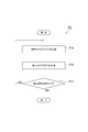
- FIG. 3 is a flowchart illustrating a method of etching according to one exemplary embodiment.
- FIG. 3 is a partial cross-sectional view of an example substrate.
- FIG. 1 schematically illustrates a plasma processing apparatus according to one exemplary embodiment.
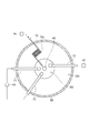
- FIG. 4 is a plan view illustrating an example of an internal configuration of a ground conductor of the plasma processing apparatus illustrated in FIG. 3.
- 3 is a flowchart showing an example of a process that can be executed in each of a step ST1 and a step ST3 shown in FIG.
- FIG. 6A is a partial cross-sectional view of an example of a substrate to which the step STa shown in FIG. 5 is applied in the step ST1 of the method MT
- FIG. 6B is a sectional view of FIG.
- FIG. 13 is a partial cross-sectional view of an example substrate to which a step STb shown in FIG.
- FIG. 9 is a partial cross-sectional view of an example of a substrate to which a step ST1 of a method MT is applied.
- FIG. 9 is a partial cross-sectional view of an example of a substrate to which a step ST2 of a method MT is applied.
- FIG. 9A is a partial cross-sectional view of an example substrate to which the process STa is applied in the process ST3 of the method MT
- FIG. 9B is a process in which the process STb is applied in the process ST3 of the method MT.
- FIG. 3 is a partial cross-sectional view of an example substrate.
- FIG. 11 is a partial cross-sectional view of an example of a substrate to which a step ST3 of a method MT is applied. It is a fragmentary sectional view of a substrate of another example.
- FIG. 12A is a partial cross-sectional view of another example of the substrate to which the process STa is applied in the process ST1 of the method MT
- FIG. 12B is a process in which the process STb is applied in the process ST1 of the method MT.
- FIG. 11 is a partial cross-sectional view of another example of the substrate. It is a fragmentary sectional view of a substrate of another example to which process ST1 of method MT was applied.
- FIG. 12A is a partial cross-sectional view of another example of the substrate to which the process STa is applied in the process ST1 of the method MT
- FIG. 12B is a process in which the process STb is applied in the process ST1 of the method MT.
- FIG. 11 is a partial cross-sectional view of another example
- FIG. 9 is a partial cross-sectional view of another example of the substrate to which the step ST2 of the method MT is applied.
- FIG. 15A is a partial cross-sectional view of another example of the substrate to which the step STa is applied in the step ST3 of the method MT
- FIG. 15B is a step STb applied in the step ST3 of the method MT.
- FIG. 11 is a partial cross-sectional view of another example of the substrate. It is a fragmentary sectional view of a substrate of another example to which process ST3 of method MT was applied.
- a method for selectively etching a first region of a substrate relative to a second region of the substrate formed from a material different from the material of the first region.
- the method includes etching the first region by plasma etching such that the first region provides its upper surface at a deeper location in the substrate than the second region.
- the method forms a carbon-containing deposit on a substrate by generating a plasma of a hydrocarbon gas in a chamber of a plasma processing apparatus having the substrate disposed therein after performing the step of etching the first region.
- the method further includes the step of:
- the method further includes, after performing the step of generating a plasma of hydrocarbon gas, further etching the first region by plasma etching.
- the electromagnet forms a magnetic field distribution having a horizontal component on the edge side of the substrate that is greater than a horizontal component on the center of the substrate.
- the deposit is formed from carbon species from a plasma of a hydrocarbon gas. Further, since the first region extends at a deeper position in the substrate than the second region, the thickness of the deposit is large on the second region and small on the first region. The first region is further etched while the second region is protected by the deposit. Therefore, the selectivity of etching the first region of the substrate with respect to the second region of the substrate is increased. Also, during the generation of the hydrocarbon gas plasma, the electromagnet forms a magnetic field distribution having a horizontal component on the edge side of the substrate that is greater than the horizontal component on the center of the substrate. Therefore, the density of the plasma on the edge side of the substrate is increased.
- the distribution of the plasma density in the radial direction is made uniform. Since carbon species from the plasma having such a distribution are deposited on the substrate, the in-plane uniformity of the thickness of the deposit is enhanced. Therefore, the in-plane uniformity of the selective etching of the first region of the substrate with respect to the second region of the substrate is improved.
- the first region may be formed from a silicon-containing material.
- the second region may be formed from a metal-containing material.
- the first region may be formed from silicon oxide and the second region may be formed from silicon nitride.
- a plasma of a processing gas including a fluorocarbon gas may be generated in a chamber in which the substrate is disposed.
- a plasma of a processing gas containing a fluorocarbon gas may be generated in a chamber in which the substrate is disposed.
- At least one of the step of etching the first region and the step of further etching the first region includes the step of forming a deposit comprising the fluorocarbon on the substrate, wherein the substrate is disposed therein.
- performing the step of forming the deposit and the step of further etching the first region may be alternately repeated.
- a plasma processing apparatus for selectively etching a first region of a substrate relative to a second region of the substrate formed from a material different than the material of the first region.
- the plasma processing apparatus includes a chamber, a substrate support, a gas supply unit, a high-frequency power supply, an electromagnet, a drive power supply, and a control unit.
- the substrate support has a lower electrode and is provided in the chamber.
- the gas supply unit is configured to supply gas into the chamber.
- the high frequency power supply is configured to generate high frequency power to excite the gas in the chamber.
- the electromagnet is configured to form a magnetic field in the interior space of the chamber.
- the drive power supply is configured to supply current to the electromagnet.
- the control unit is configured to control the gas supply unit, the high frequency power supply, and the drive power supply.
- the control unit is configured to execute the first control, the second control, and the third control.
- the first control is to control the gas supply and the high frequency power supply to etch the first region by plasma etching such that the first region provides its upper surface at a deeper position in the substrate than the second region.
- the second control is to control the gas supply unit and the high-frequency power source to generate a plasma of a hydrocarbon gas after the first region is etched, so as to form a carbon-containing deposit on the second region.
- the third control includes controlling the gas supply unit and the high-frequency power supply to further etch the first region by plasma etching after forming the deposit on the second region.
- the second control is that during the generation of the plasma of the hydrocarbon gas, the electromagnet is driven to form a magnetic field distribution having a horizontal component on the edge side of the substrate that is greater than the horizontal component on the center of the substrate. Including controlling the power supply.
- the first region may be formed from a silicon-containing material.
- the first control may include controlling the gas supply and the high frequency power supply to generate a plasma of the processing gas including the fluorocarbon gas in the chamber.
- the third control may include controlling the gas supply unit and the high frequency power supply to generate a plasma of the processing gas including the fluorocarbon gas in the chamber.
- the first region may be formed from a silicon-containing material.
- At least one of the first control and the third control includes a gas supply unit and a gas supply unit configured to generate a plasma of a processing gas including a fluorocarbon gas in the chamber to form a deposit including the fluorocarbon on the substrate.
- a gas supply unit and a gas supply unit configured to generate a plasma of a processing gas including a fluorocarbon gas in the chamber to form a deposit including the fluorocarbon on the substrate.
- control unit may alternately repeat the second control and the third control.
- FIG. 1 is a flowchart illustrating a method of etching according to one exemplary embodiment.
- An etching method according to an embodiment (hereinafter, referred to as “method MT”) is performed to selectively etch a first region of a substrate with respect to a second region.
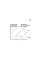
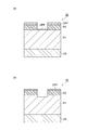
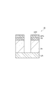
- FIG. 2 is a partial cross-sectional view of one example of a substrate.
- the example substrate W shown in FIG. 2 can be processed by the method MT.
- the substrate W may have a disk shape like a wafer.
- the substrate W has a first region R1 and a second region R2.
- the substrate W may further have a base region UR.
- the first region R1 and the second region R2 are provided on the base region UR.
- the first region R1 is provided on the base region UR
- the second region R2 is provided on the first region R1.
- the second region R2 is patterned like a mask. That is, the second region R2 provides an opening.
- the first region R1 may be formed to fill a recess provided by the second region R2. Further, the first region R1 may be formed so as to cover the second region.
- the first region R1 is a region to be selectively etched.
- the second region R2 is formed from a material different from the material of the first region R1.
- the material of the first region R1 and the material of the second region R2 are not limited.
- the first region R1 is formed from, for example, a silicon-containing material.
- the silicon-containing material of the first region R1 is, for example, SiO 2 .
- the silicon-containing material of the first region R1 may be a low dielectric constant material.
- the low dielectric constant material is, for example, SiOC or SiOCH.
- the second region R2 is formed of, for example, a metal-containing material.
- the metal-containing material is, for example, any one of titanium, tungsten, zirconium, aluminum, tantalum, cobalt, and ruthenium, or an oxide, nitride, or carbide of the metal material.
- the second region R2 may be formed from silicon nitride.
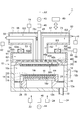
- FIG. 3 is a diagram schematically illustrating a plasma processing apparatus according to one exemplary embodiment.
- the chamber 10 is a container that provides an internal space 10s.
- the chamber 10 has a substantially cylindrical shape.
- the central axis AX shown in FIG. 3 is the central axis of the chamber 10 and the internal space 10s.
- the chamber 10 has a chamber body 12.
- the chamber main body 12 has a substantially cylindrical shape.
- the internal space 10 s of the chamber 10 is provided inside the chamber main body 12.
- the chamber body 12 includes a side wall 12a and a bottom 12b.
- the side wall 12a forms a side wall of the chamber 10.
- the bottom 12b constitutes the bottom of the chamber 10.
- the chamber main body 12 is formed of a metal such as aluminum, for example.
- a film having plasma resistance is formed on the inner wall surface of the chamber body 12. This film may be a ceramic film such as an alumite film or a yttrium oxide film.
- the chamber body 12 is grounded.
- a passage 12p is formed in the side wall 12a.
- the substrate W passes through the passage 12p when transported between the internal space 10s and the outside of the chamber 10.
- the passage 12p can be opened and closed by a gate valve 12g.
- the gate valve 12g is provided along the side wall 12a.
- a substrate support that is, a support 14 is provided in the internal space 10s.
- the support 14 is supported by a support 15.
- the support 15 has a cylindrical shape.
- the support 15 extends upward from the bottom 12 b of the chamber body 12.
- the support 15 has an insulating property.
- the support 15 is made of, for example, ceramic.
- the support 14 is configured to support the substrate W.
- the support 14 shares the central axis AX with the chamber 10.
- the support 14 provides a mounting area 14r.
- the center of the mounting area 14r is located on the central axis AX.
- the substrate W is mounted on the mounting area 14r such that the center thereof is located on the central axis AX.
- the support 14 includes the electrode plate 16, the lower electrode 18, and the electrostatic chuck 20.
- the electrode plate 16 has a substantially disk shape.
- the electrode plate 16 has conductivity.
- the electrode plate 16 is formed from a metal such as aluminum.
- the lower electrode 18 has a disk shape.
- the lower electrode 18 has conductivity.
- the lower electrode 18 is formed from a metal such as aluminum.
- the lower electrode 18 is mounted on the electrode plate 16. The lower electrode 18 is electrically connected to the electrode plate 16.
- a channel 18p is formed in the lower electrode 18.
- the flow path 18p extends, for example, in a spiral shape in the lower electrode 18.
- a heat exchange medium (for example, a refrigerant) is supplied to the flow path 18p from a heat exchange medium circulation device 22 (for example, a chiller unit).
- the circulation device 22 is provided outside the chamber 10.
- the heat exchange medium supplied to the flow path 18p is returned to the circulation device 22.
- the heat exchange between the heat exchange medium and the lower electrode 18 controls the temperature of the substrate W placed on the support 14.
- the electrostatic chuck 20 is provided on the lower electrode 18.
- the electrostatic chuck 20 has a substantially disk shape.
- the electrostatic chuck 20 has a main body and electrodes.
- the main body of the electrostatic chuck 20 is made of a dielectric (for example, ceramic).
- the electrodes of the electrostatic chuck 20 are conductive films and are provided in the main body of the electrostatic chuck 20.
- a DC power supply 24 is connected to the electrodes of the electrostatic chuck 20 via a switch.
- the electrostatic chuck 20 provides the mounting area 14r described above.
- the plasma processing apparatus 1 may be provided with a heat transfer gas supply line for supplying a heat transfer gas (for example, He gas) between the electrostatic chuck 20 and the lower surface of the substrate W.
- a heat transfer gas for example, He gas
- One or more heaters may be provided inside the electrostatic chuck 20.
- the one or more heaters When power is supplied from the heater controller to one or more heaters, the one or more heaters generate heat, and the temperature of the electrostatic chuck 20 and thus the temperature of the substrate W are adjusted.
- a focus ring FR is mounted on the support base 14.
- the focus ring FR is arranged so as to surround the electrostatic chuck 20 and the edge of the substrate W.
- the focus ring FR is an annular plate and is formed from a silicon-containing material such as silicon or quartz. The focus ring FR is used to obtain uniform plasma processing.
- a cylindrical conductor 26 is provided.
- the conductor 26 is grounded.
- a cylindrical insulator 28 is provided above the conductor 26 so as to surround the support 14.
- the insulator 28 is formed from a ceramic such as quartz.
- An exhaust path is formed between the support 14 and the side wall 12a of the chamber body 12.
- a baffle plate 30 is provided in the exhaust path.
- the baffle plate 30 is an annular plate.
- the baffle plate 30 has a plurality of holes penetrating the baffle plate 30 in the plate thickness direction.
- the baffle plate 30 is formed by forming a plasma-resistant film such as yttrium oxide on the surface of a member formed of a metal such as aluminum.
- the exhaust pipe 32 is connected to the bottom 12b of the chamber body 12.
- the exhaust pipe 32 can communicate with an exhaust path.
- An exhaust device 34 is connected to the exhaust pipe 32.
- the exhaust device 34 includes an automatic pressure control valve and a pressure reducing pump such as a turbo molecular pump. By operating the exhaust device 34, the pressure of the internal space 10s is set to the specified pressure.
- An upper electrode 36 is provided above the support base 14. Part of the internal space 10 s is interposed between the upper electrode 36 and the support 14. The upper electrode 36 is provided so as to close an upper opening of the chamber body 12.
- a member 37 is interposed between the upper electrode 36 and the upper end of the chamber body 12.
- the member 37 is formed from an insulating material. Member 37 may be formed from ceramic, for example, quartz. In one embodiment, the member 37 and a part of a ground conductor described below may be interposed between the upper electrode 36 and the upper end of the chamber body 12.
- the upper electrode 36 constitutes a shower head.
- the upper electrode 36 includes a top plate 38 and a support 40 in one embodiment.
- the top plate 38 is formed of, for example, silicon.
- the top plate 38 is formed by providing a coating made of ceramic such as yttrium oxide on the surface of a member made of aluminum.
- the top plate 38 has a plurality of gas discharge ports 38h penetrating the top plate 38 in the thickness direction.
- the support 40 is provided on the top plate 38.
- the support 40 is configured to detachably support the top plate 38.
- the support 40 is formed from a conductive material such as aluminum. Inside the support body 40, a gas diffusion chamber 40d is formed.
- the support 40 has a plurality of holes 40h. The plurality of holes 40h extend downward from the gas diffusion chamber 40d. Each of the plurality of holes 40h communicates with the plurality of gas discharge ports 38h.
- the gas supply unit 41 is connected to the gas diffusion chamber 40d.
- the gas supply unit 41 is configured to supply gas into the chamber 10, that is, into the internal space 10s.
- the gas supply unit 41 is configured to be able to output a plurality of gases used in the method MT.
- the plurality of gases used in the method MT include a fluorocarbon gas, a noble gas, and a hydrocarbon gas.
- the fluorocarbon gas includes, for example, one or more of a C 4 F 6 gas, a C 4 F 8 gas, and a C 6 F 8 gas, but may be another fluorocarbon gas.
- the rare gas is, for example, Ar gas, but may be another rare gas.
- the hydrocarbon gas is, for example, CH 4 gas, but may be a hydrocarbon gas other than CH 4 gas.
- the plurality of gases used in the method MT may further include other gases.
- the plurality of gases used in the method MT may further include one or more of nitrogen gas (N 2 gas) and oxygen-containing gas (eg, O 2 gas or CO gas).
- the gas supply unit 41 has a plurality of flow controllers and a plurality of valves.
- the gas supply unit 41 is configured to individually adjust the flow rate of one or more gases to be output.
- the gas output from the gas supply unit 41 is discharged from the plurality of gas discharge ports 38h to the internal space 10s through the gas diffusion chamber 40d and the plurality of holes 40h.
- a channel 40p is formed in the support 40.
- the chiller unit 42 is connected to the flow path 40p.
- a coolant such as cooling water is circulated between the flow path 40p and the chiller unit 42.
- the temperature of the upper electrode 36 is adjusted by heat exchange between the refrigerant supplied to the flow path 40p from the chiller unit 42 and the upper electrode 36.
- the plasma processing apparatus 1 further includes a first high-frequency power supply 43 and a second high-frequency power supply 44.
- the first high-frequency power supply 43 and the second high-frequency power supply 44 are provided outside the chamber 10.
- the first high frequency power supply 43 is configured to generate a first high frequency power mainly for generating plasma.
- the frequency of the first high-frequency power is not limited, but is, for example, 100 MHz.
- the first high frequency power supply 43 is electrically connected to the upper electrode 36 via the matching unit 45 and the power supply conductor 48.
- the matching unit 45 has a matching circuit for matching the output impedance of the first high-frequency power supply 43 with the impedance on the load side (upper electrode 36 side).
- the power supply conductor 48 is connected at its lower end to the upper electrode 36.
- the power supply conductor 48 extends upward from the upper electrode 36.
- the power supply conductor 48 is a cylindrical or rod-shaped conductor, and its central axis substantially coincides with the central axis AX. Note that the first high-frequency power supply 43 may be electrically connected to the lower electrode 18 via the matching unit 45 instead of the upper electrode 36.
- the second high-frequency power supply 44 is configured to generate a second high-frequency power mainly for drawing ions into the substrate W, that is, a high-frequency power for bias.
- the frequency of the second high frequency power is lower than the frequency of the first high frequency power.
- the frequency of the second high frequency power may be higher than 13.56 MH.
- the frequency of the second high frequency power may be equal to or higher than 40 MHz.
- the frequency of the second high frequency power may be 60 MHz or more.
- the second high frequency power supply 44 is electrically connected to the lower electrode 18 via a matching unit 46.
- the matching unit 46 has a matching circuit for matching the output impedance of the second high-frequency power supply 44 with the impedance on the load side (the lower electrode 18 side).
- the plasma processing apparatus 1 further includes a ground conductor 50.
- the ground conductor 50 has conductivity.
- the ground conductor 50 is formed from a metal such as aluminum.
- the ground conductor 50 is grounded.
- the ground conductor 50 extends so as to cover the upper electrode 36 above the chamber main body 12.
- the power supply conductor 48 extends upward through a space surrounded by the ground conductor 50 and is connected to the first high-frequency power supply 43 via the matching unit 45 outside the ground conductor 50.
- a distribution of electric field intensity having a high electric field intensity above the center of the substrate W and a low electric field intensity above the edge side of the substrate W may be formed. That is, in the internal space 10s, a non-uniform electric field intensity distribution can be formed in which the electric field intensity decreases as the distance from the central axis AX in the radiation direction (ie, the radial direction) increases. Under a non-uniform electric field intensity distribution, the plasma density is high near the central axis AX and low at locations away from the central axis AX. That is, a non-uniform plasma density distribution is formed in the radiation direction with respect to the central axis AX.
- the plasma processing apparatus 1 further includes an electromagnet 60 to obtain a uniform plasma density distribution.
- the electromagnet 60 is disposed above the upper electrode 36.
- the electromagnet 60 forms a magnetic field distribution having a horizontal component larger than the horizontal component on the central axis AX at a position away from the central axis AX in the internal space 10s. That is, the electromagnet 60 forms a distribution of a magnetic field having a horizontal component whose magnitude increases as the distance from the central axis AX in the radial direction increases in the internal space 10s.
- the residence time of the electrons becomes longer.
- the density of the plasma increases at a portion where a magnetic field having a large horizontal component is formed. Therefore, according to the plasma processing apparatus 1, a uniform plasma density distribution can be obtained in the radial direction with respect to the central axis AX. Therefore, according to the plasma processing apparatus 1, the in-plane uniformity of the processing for the substrate W is improved.
- the electromagnet 60 has the yoke 62 and the coil 64.
- the yoke 62 is formed from a magnetic material.
- the yoke 62 has a base portion 62a and a plurality of cylindrical portions 62b.
- the base portion 62a has a substantially annular shape and a substantially plate shape, and extends in a direction orthogonal to the central axis AX.
- Each of the plurality of tubular portions 62b has a tubular shape, and extends downward from the base portion 62a.
- the plurality of cylindrical portions 62b are provided coaxially with the center axis AX.
- the coil 64 is wound around the central axis AX.
- the coil 64 is provided between two cylindrical portions 62b that are adjacent in the radial direction.
- the electromagnet 60 can have one or more coils 64.
- the plural coils 64 are provided coaxially with the central axis AX.
- the coil 64 of the electromagnet 60 is connected to the drive power source 66 via the wiring 68.
- a current from the driving power supply 66 is applied to the coil 64, a magnetic field is formed by the electromagnet 60.
- the effect of confining electrons in the radiation direction (radial direction) (the effect of suppressing the diffusion of electrons) and the effect of suppressing the disappearance of electrons (the effect on the electrodes) And the effect of suppressing the arrival of electrons) are satisfactorily compatible. Therefore, the density of the plasma is increased at the location.
- the electromagnet 60 when the radius of the substrate W is, for example, 150 mm, the electromagnet 60 operates so that the distance between the position where the angle of the magnetic field vector is 45 ° and the central axis AX is 135 mm or more and 185 mm or less. Can be configured.
- the average value of the inner diameter and the outer diameter of one coil 64 of the electromagnet 60 is set to be equal to or greater than the distance between the central axis AX and the edge of the substrate W.
- the average value of the inner and outer diameters of one coil 64 of the electromagnet 60 is set to 150 mm or more and 250 mm or less.
- the angle of the magnetic field vector is 0 ° when the magnetic field has only a downward component, and is 90 ° when the magnetic field has only a radial component (horizontal component). Thus, if the angle of the magnetic field vector is 45 °, the magnetic field has both horizontal and vertical components.
- the electromagnet 60 When the electromagnet 60 is disposed in a space surrounded by the ground conductor that covers the upper electrode, the first high-frequency power is applied to the electromagnet 60 and / or wiring that connects the electromagnet 60 and a power supply (drive power supply). Inflow. As a result, the electric field strength in the internal space 10s locally fluctuates. Therefore, the electromagnet 60 is arranged outside the ground conductor. However, if the electromagnet 60 is arranged in a space above the upper end of the ground conductor, the distance in the vertical direction from the electromagnet 60 to the internal space 10s becomes longer. A sufficiently large magnetic field cannot be efficiently formed therein.
- the ground conductor 50 provides an external space ES in which the electromagnet 60 is disposed. ing.
- the outer space ES is closer to the inner space 10s than the upper end of the ground conductor 50, is separated upward from the upper electrode 36, and is shielded from the upper electrode 36 by the ground conductor 50.
- the ground conductor 50 includes a first portion 51, a second portion 52, and a third portion 53.
- the first portion 51 has a cylindrical shape.
- the central axis of the first portion 51 substantially coincides with the central axis AX.
- the first portion 51 extends upward from the chamber body 12. In the example shown in FIG. 3, the first portion 51 extends upward from the upper end of the side wall 12a of the chamber body 12.
- the lower end of the first portion 51 is interposed between the member 37 and the upper end of the side wall 12a.
- the second portion 52 is spaced upward from the upper electrode 36 and extends from the first portion 51 toward the central axis AX.
- the second portion 52 has a plate shape extending in a direction intersecting or orthogonal to the central axis AX.
- the first portion 51 and the second portion 52 provide a first space IS1 above the upper electrode 36.
- the first space IS1 is a part of a space inside the ground conductor 50 (that is, on the upper electrode 36 side).
- the first space IS1 ensures a distance between the upper electrode 36 and the ground conductor 50 in the vertical direction. Therefore, capacitive coupling between the ground conductor 50 and the upper electrode 36 is suppressed.
- the vertical distance between the upper surface of the upper electrode 36 and the lower surface of the second portion 52 of the ground conductor 50 is set to, for example, 60 mm or more.
- the third portion 53 has a cylindrical shape.
- the central axis of the third portion 53 is substantially coincident with the central axis AX.
- the third portion 53 extends closer to the central axis than the first portion 51.
- the third portion 53 extends upward from the second portion 52.
- the third portion 53 provides a second space IS2.
- the second space IS2 is a space inside the second portion 52, and is a part of a space inside the ground conductor 50 (that is, on the upper electrode 36 side).
- the second space IS2 is continuous with the first space IS1.
- the power supply conductor 48 extends upward through the first space IS1 and the second space IS2.
- the external space ES is provided by the ground conductor 50 outside the third portion 53, on the second portion 52, and above the internal space 10s.
- the external space ES extends in the circumferential direction around the central axis AX on the outside of the third portion 53 and on the second portion 52.
- An electromagnet 60 is arranged in the external space ES. Note that the vertical distance between the lower end of the electromagnet 60 disposed in the external space ES and the upper surface of the upper electrode 36 is larger than 60 mm. Further, the vertical distance between the lower end of the electromagnet 60 and the substrate W placed on the support 14 may be 230 mm or less.
- the distance between the electromagnet 60 arranged in the outer space ES and the inner space 10s is relatively short. Further, as described above, the electromagnet 60 forms a magnetic field distribution having a low horizontal component near the central axis AX and a large horizontal component at a position distant from the central axis in the internal space 10s. Therefore, the distribution of the magnetic field suitable for obtaining a uniform plasma density distribution can be efficiently formed in the internal space 10s by the electromagnet 60 disposed outside the ground conductor 50.
- the drive power supply 66 is connected to the coil 64 of the electromagnet 60 as described above.
- the electromagnet 60 and the drive power supply 66 are arranged outside the ground conductor 50. Therefore, a filter for preventing the high frequency from flowing into the drive power supply 66 may not be provided between the coil 64 and the drive power supply 66.
- the ground conductor 50 further includes a fourth portion 54, a fifth portion 55, and a sixth portion 56.
- the fourth part 54 extends from the third part 53 in a radial direction with respect to the central axis AX above the second part 52.
- the fourth portion 54 has a plate shape extending in a direction intersecting or orthogonal to the central axis AX.
- the fifth portion 55 has a cylindrical shape.
- the central axis of the fifth portion 55 substantially coincides with the central axis AX.
- the fifth portion 55 is farther from the central axis than the third portion 53 and extends upward from the fourth portion 54.
- the sixth portion 56 extends from the fifth portion 55 toward the central axis AX above the fourth portion 54.
- the sixth portion 56 has a plate shape extending in a direction intersecting or orthogonal to the central axis AX.
- the ground conductor 50 further has a lid 57 extending from the sixth portion to the vicinity of the power supply conductor 48.
- the fourth portion 54, the fifth portion 55, and the sixth portion 56 provide a third space IS3.
- the third space IS3 is a space surrounded by the fourth portion 54, the fifth portion 55, and the sixth portion 56, and is a part of the space inside the ground conductor 50.
- the third space IS3 is continuous with the second space IS2.
- the power supply conductor 48 extends upward through the third space IS3.
- the first to sixth portions are formed of three members, but the number of members forming the ground conductor 50 may be any number.
- the plasma processing apparatus 1 further includes a tube 71 as shown in FIGS.
- the tube 71 extends upward from the upper electrode 36 through the first space IS1 and the second space IS2, and extends through the third space IS3 to the side and outside with respect to the ground conductor 50.
- the tube 71 is connected to the chiller unit 42 outside the ground conductor 50.
- the refrigerant from the chiller unit 42 is supplied to the flow path 40p via the pipe 71.
- the tube 71 is substantially shielded from the upper electrode 36 by the fourth portion 54 of the ground conductor 50.
- the plasma processing apparatus 1 further includes a tube 72.
- the tube 72 extends upward through the first space IS1 and the second space IS2, and extends laterally and outwardly with respect to the ground conductor 50 through the third space IS3.
- the tube 72 is connected to the chiller unit 42 outside the ground conductor 50.
- the refrigerant is returned from the flow path 40p to the chiller unit 42 via the pipe 72.
- the tube 72 is substantially shielded from the upper electrode 36 by the fourth portion 54 of the ground conductor 50.
- the plasma processing apparatus 1 further includes a tube 73.
- the tube 73 extends upward from the upper electrode 36 through the first space IS1 and the second space IS2, and extends laterally and outwardly to the ground conductor 50 through the third space IS3. .
- the tube 73 is connected to the gas supply unit 41 outside the ground conductor 50.
- the gas output from the gas supply unit 41 is supplied to the upper electrode 36, that is, the shower head via the tube 73.
- the tube 73 is substantially shielded from the upper electrode 36 by the fourth portion 54 of the ground conductor 50.
- the gas supply unit 41 and the upper electrode 36 may be connected to each other via a plurality of tubes.
- the plasma processing apparatus 1 further includes a DC power supply 74 and a wiring 75.
- the DC power supply 74 is configured to generate a negative DC voltage applied to the upper electrode 36.
- the wiring 75 connects the DC power supply 74 and the upper electrode 36 to each other.
- the wiring 75 may include a coil 75c.
- the coil 75c is provided in the third space IS3.
- the wiring 75 extends upward from the upper electrode 36 through the first space IS1 and the second space IS2, and extends to the side and outside of the ground conductor 50 through the third space IS3.
- the wiring 75 is electrically insulated from the fifth portion 55 and the ground conductor 50.
- the wiring 75 is connected to a DC power supply 74 outside the ground conductor 50. In the third space IS3, the wiring 75 is substantially shielded from the upper electrode 36 by the fourth portion 54 of the ground conductor 50.
- the plasma processing apparatus 1 further includes a control unit 80.
- the control unit 80 is configured to control each unit of the plasma processing apparatus 1.
- the control unit 80 can be a computer device.
- the controller 80 may include a processor, a storage device such as a memory, an input device such as a keyboard, a mouse, and a touch panel, a display device, a control signal input / output interface, and the like.
- the storage device stores a control program and recipe data.
- the processor of the control unit 80 executes the control program and sends out a control signal to control each unit of the plasma processing apparatus 1 according to the recipe data.
- the control unit 80 can control each unit of the plasma processing apparatus 1 for performing the method MT.
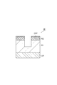
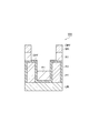
- FIG. 5 is a flowchart showing an example of processing that can be executed in each of the steps ST1 and ST3 shown in FIG.
- FIG. 6A is a partial cross-sectional view of an example of a substrate to which the step STa shown in FIG. 5 is applied in the step ST1 of the method MT
- FIG. 6B is a sectional view of FIG. 13 is a partial cross-sectional view of an example substrate to which a step STb shown in FIG.
- FIG. 7 is a partial cross-sectional view of an example of the substrate to which the step ST1 of the method MT is applied.
- FIG. 6A is a partial cross-sectional view of an example of a substrate to which the step STa shown in FIG. 5 is applied in the step ST1 of the method MT
- FIG. 6B is a sectional view of FIG. 13 is a partial cross-sectional view of an example substrate to which a step STb shown in FIG.
- FIG. 7 is a partial cross-sectional view of an example of
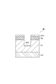
- FIG. 8 is a partial cross-sectional view of an example of the substrate to which the step ST2 of the method MT is applied.
- FIG. 9A is a partial cross-sectional view of an example of a substrate to which the process STa is applied in the process ST3 of the method MT
- FIG. 9B is a process in which the process STb is applied in the process ST3 of the method MT.
- FIG. 3 is a partial cross-sectional view of an example substrate.
- FIG. 10 is a partial cross-sectional view of an example of the substrate to which the step ST3 of the method MT is applied.
- the method MT will be described in detail with an example in which the method MT is applied to the substrate W illustrated in FIG. 2 using the plasma processing apparatus 1.
- control of each unit of the plasma processing apparatus 1 by the control unit 80 will be described.
- the substrate W is placed on the support base 14 (on the electrostatic chuck 20) and is held by the electrostatic chuck 20. Then, in the method MT, the step ST1 is performed.
- the first region R1 is etched by plasma etching.
- the first region R1 is selectively etched with respect to the second region R2.
- the first region R1 is etched so as to provide its upper surface at a deeper position in the substrate W than the second region R2.
- the control unit 80 executes the first control to execute the process ST1.
- the control unit 80 controls the gas supply unit 41 and the first high-frequency power supply 43 and / or the second high-frequency power supply 44.
- the control unit 80 further controls the exhaust device 34 so as to adjust the pressure in the chamber 10.
- the first region R1 is etched by the plasma etching such that the first region R1 provides its upper surface at a deeper position in the substrate W than the second region R2.
- the processing PE shown in FIG. 5 is executed in step ST1.
- the processing PE includes a step STa and a step STb.
- step STa plasma of a processing gas containing a fluorocarbon gas is generated in the chamber 10.
- step STa fluorocarbon from the generated plasma is deposited on the substrate W to form a deposit DPF on the substrate W.
- the deposit DPF is formed on the substrate W, for example, as shown in FIG.
- the fluorocarbon gas used in the step STa may include one or more of a C 4 F 6 gas, a C 4 F 8 gas, and a C 6 F 8 gas.
- the processing gas used in the step STa may further include one or more other gases in addition to the fluorocarbon gas.
- the processing gas used in the step STa further includes a rare gas (for example, Ar gas) in addition to the fluorocarbon gas. May be included.
- the processing gas used in the process STa is a rare gas (for example, Ar gas) in addition to the fluorocarbon gas. And nitrogen gas (N 2 gas).
- the processing gas used in the step STa may further include a rare gas (for example, an Ar gas) in addition to the fluorocarbon gas.
- a rare gas for example, Ar gas
- an oxygen-containing gas for example, O 2
- control A controls the gas supply unit 41 to supply the processing gas into the chamber 10 and supplies the first high-frequency power. And controlling the first high frequency power supply 43.
- the control A controls the exhaust device 34 to set the pressure in the chamber 10 to the specified pressure.
- the control A may further include controlling the second high frequency power supply 44 so as to stop outputting the second high frequency power.
- the control A may further include controlling the second high frequency power supply 44 to supply the second high frequency power.
- step STa the power level of the second high-frequency power is set to a level lower than the power level of the second high-frequency power in step STb described below.
- the first control includes control A.
- a rare gas plasma is generated in the chamber 10.
- a rare gas is supplied into the chamber 10.
- an N 2 gas and / or an O 2 gas may be supplied into the chamber 10 in addition to the rare gas.
- a mixed gas of Ar gas, N 2 gas and Ar gas, or N 2 gas a mixed gas of Ar gas, N 2 gas and Ar gas, or N 2 gas, A mixed gas of O 2 gas and Ar gas may be supplied into the chamber 10.
- an Ar gas may be supplied into the chamber 10 in step STb.
- step STb rare gas ions from the rare gas plasma are supplied to the substrate W.
- the fluorocarbon in the deposit DPF existing on the first region R1 reacts with the material constituting the first region R1, and the first region R1 is etched.
- the second region R2 is protected by the deposit DPF existing thereon.
- the step STb in the step ST1 for example, as shown in FIG. 6B, the first region R1 is etched.
- control B controls the gas supply unit 41 to supply the above-described gas including a rare gas into the chamber 10, and performs the first This includes controlling the first high frequency power supply 43 to supply high frequency power.
- the control B further includes controlling the second high frequency power supply 44 to supply the second high frequency power.
- the control B further includes controlling the exhaust device 34 to set the pressure in the chamber 10 to the specified pressure.
- Step STa and Step STb are alternately repeated.
- the control unit 80 repeatedly executes a control sequence including the control A and the control B so that the process STa and the process STb are alternately repeated.
- a step STc is performed.
- the stop condition is a condition used for determining whether or not to stop the alternate repetition of the process STa and the process STb.
- the stop condition is satisfied, for example, when the number of times of alternately repeating the process STa and the process STb reaches a predetermined number. If it is determined in step STc that the stop condition is not satisfied, step STa and step STb are sequentially performed again.
- step STc the execution of the processing PE ends.
- each of the steps STa and STb may be performed only once. In this case, the processing PE does not include the step STc.
- the second region R2 is protected by the deposit DPF formed thereon. Therefore, the etching of the second region R2 accompanying the etching of the first region R1 is suppressed.
- the substrate W is processed into a shape as shown in FIG. That is, the substrate W is processed such that the first region R1 provides its upper surface at a deeper position in the substrate W than the second region R2.
- step ST1 plasma of a processing gas containing a fluorocarbon gas may be generated in the chamber 10 in which the substrate W is disposed.
- the first region R1 can be etched by active species of fluorocarbon and / or active species of fluorine that collide with the substrate W from the plasma.
- the control unit 80 controls the gas supply unit 41 so as to supply the processing gas into the chamber 10. Further, in the first control for performing the process ST1 of this embodiment, the control unit 80 controls the exhaust device 34 so as to set the pressure in the chamber 10 to the specified pressure.
- control unit 80 controls the first high-frequency power supply 43 so as to supply the first high-frequency power, and controls the second high-frequency power.
- the second high frequency power supply 44 is controlled so as to be supplied.
- step ST2 is executed.
- the substrate W to which the process ST1 has been applied is housed in the chamber 10.
- a plasma of a hydrocarbon gas is generated in the chamber 10.
- a hydrocarbon gas is supplied into the chamber 10.
- the hydrocarbon gas is, for example, but not limited to, a CH 4 gas.
- a rare gas for example, Ar gas
- the gas supplied into the chamber 10 is excited to generate plasma.
- step ST2 a distribution of a magnetic field is formed in the chamber 10 by the electromagnet 60 while the plasma is being generated.
- the electromagnet 60 forms a magnetic field distribution having a horizontal component on the edge side of the substrate that is larger than the horizontal component on the center of the substrate W.
- step ST2 a deposit DPC containing carbon from the plasma is formed on the substrate W as shown in FIG.
- the first region R1 extends at a deeper position in the substrate W than the second region R2. Therefore, the thickness of the deposit DPC is large on the second region R2 and small on the first region R1.
- the above-described magnetic field is formed in the chamber 10 by the electromagnet 60, a uniform plasma density distribution can be obtained in the radial direction with respect to the central axis AX. Since carbon species from the plasma having such a distribution is deposited on the substrate W, the in-plane uniformity of the thickness of the deposit DPC is enhanced.
- the deposit DPF that may be left on the substrate W after the end of the step ST1 is omitted.
- the control unit 80 executes the second control to execute the process ST2.
- the control unit 80 controls the gas supply unit 41 to supply the above-described gas including the hydrocarbon gas into the chamber 10, and controls the first high-frequency power to supply the first high-frequency power.
- the power supply 43 is controlled.
- the control unit 80 further controls the exhaust device 34 so as to set the pressure in the chamber 10 to the specified pressure.
- the control unit 80 further controls the drive power supply 66 so that the electromagnet 60 forms the above-described magnetic field distribution.
- the control unit 80 may further control the second high-frequency power supply 44 to stop outputting the second high-frequency power.
- control unit 80 may further control the second high-frequency power supply 44 so as to supply the second high-frequency power.
- the power level of the second high-frequency power in the second control is set to a low level so as to suppress physical etching of the substrate W due to ion collision.
- Step ST3 can be executed in a state where the substrate W to which step ST2 has been applied is arranged in the chamber 10.
- the first region R1 is further etched by plasma etching.
- the first region R1 is selectively etched with respect to the second region R2.
- the control unit 80 executes a third control.
- the control unit 80 controls the gas supply unit 41 and the first high-frequency power supply 43 and / or the second high-frequency power supply 44.
- the control unit 80 further controls the exhaust device 34 so as to adjust the pressure in the chamber 10.
- the first region R1 is further etched by the plasma etching.
- step ST3 the processing PE described above in relation to step ST1 may be executed.
- plasma of a processing gas containing a fluorocarbon gas is generated in the chamber 10 in step STa.
- fluorocarbon from the generated plasma is deposited on the substrate W to form a deposit DPF on the substrate W.
- the deposit DPF is formed on the substrate W, for example, as shown in FIG.
- the control by the control unit 80 for executing the step STa in the step ST3 is the control A described above.
- step STb When the processing PE is performed in step ST3, plasma of a rare gas is generated in the chamber 10 in step STb.
- a rare gas is supplied into the chamber 10.
- an N 2 gas and / or an O 2 gas may be supplied into the chamber 10 in addition to the rare gas.
- step STb rare gas ions from the rare gas plasma are supplied to the substrate W.
- the fluorocarbon in the deposit DPF existing on the first region R1 reacts with the material constituting the first region R1, and the first region R1 is etched.
- the second region R2 is protected by the deposit DPF existing thereon.
- the step STb in the step ST3 for example, as shown in FIG. 9B, the first region R1 is etched.
- the control by the control unit 80 for performing the step STb in the step ST3 is the above-described control B.
- a sequence including the steps STa and STb may be performed one or more times.
- the control unit 80 may execute the control sequence including the control A and the control B one or more times in order to execute the processing PE in the process ST3.
- step ST3 plasma of a processing gas containing a fluorocarbon gas may be generated in the chamber 10 in which the substrate W is disposed.
- the first region R1 can be etched by active species of fluorocarbon and / or active species of fluorine that collide with the substrate W from the plasma.
- the control unit 80 controls the gas supply unit 41 so as to supply the processing gas into the chamber 10.
- the control unit 80 controls the exhaust device 34 to set the pressure in the chamber 10 to the specified pressure.
- control unit 80 controls the first high-frequency power supply 43 so as to supply the first high-frequency power, and controls the second high-frequency power.
- the second high frequency power supply 44 is controlled so as to be supplied.
- step ST2 and step ST3 are alternately repeated.
- the control unit 80 repeatedly executes the second control and the third control alternately.
- step ST4 is performed.
- step ST4 it is determined whether or not a stop condition is satisfied.
- the stop condition is a condition used for determining whether or not to stop alternate repetition of step ST2 and step ST3.
- the stop condition is satisfied, for example, when the number of times of alternately repeating steps ST2 and ST3 has reached a predetermined number. If it is determined in step ST4 that the stop condition is not satisfied, steps ST2 and ST3 are performed again in order.
- the method MT ends. As a result, as shown in FIG. 10, the first region R1 is etched. Note that each of the steps ST2 and ST3 may be performed only once. In this case, the method MT does not include the step ST4.
- the deposit DPC is formed from carbon species from a plasma of a hydrocarbon gas.
- the first region R1 extends at a deeper position in the substrate W than the second region R2, so that the thickness of the deposit DPC is higher than the second region R2. Is larger and smaller on the first region R1.
- the first region R1 is further etched while the second region R2 is protected by the deposit DPC. Therefore, the selectivity of the etching of the first region R1 of the substrate W with respect to the second region R2 of the substrate W is increased.
- the electromagnet 60 forms a magnetic field distribution having a horizontal component on the edge side of the substrate W that is larger than the horizontal component on the center of the substrate W. Therefore, the density of the plasma on the edge side of the substrate W is increased. As a result, the distribution of the plasma density in the radial direction is made uniform. Since carbon species from the plasma having such a distribution is deposited on the substrate W, the in-plane uniformity of the thickness of the deposit DPC is enhanced. Therefore, the in-plane uniformity of the selective etching of the first region R1 of the substrate W with respect to the second region R2 of the substrate W is improved.
- step ST2 and step ST3 are alternately repeated. That is, in this embodiment, the formation of the deposit DPC and the etching of the first region R1 are alternately repeated. According to this embodiment, the deposit DPC is reformed on the substrate W before the further execution of the step ST3. Therefore, the etching of the second region R2 is further suppressed, and the selectivity of the etching of the first region R1 is further increased.
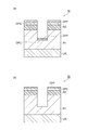
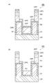
- FIG. 11 is a partial cross-sectional view of another example substrate.
- the method MT can be applied to the substrate WA shown in FIG.
- the substrate WA has a base region UR, a first region R1, and a second region R2.
- the substrate WA is a product obtained during the manufacture of the fin field effect transistor.
- the base region UR is formed of, for example, polycrystalline silicon.
- the base region UR is a fin region in one example, and has a substantially rectangular parallelepiped shape.
- the substrate WA has a plurality of protrusions PT.
- the plurality of protrusions PT are provided on the base region UR, and are arranged substantially parallel to each other.
- each of the plurality of protrusions PT is a gate region.
- the second region R2 is formed from silicon nitride.
- the second region R2 is provided so as to cover the plurality of protrusions PT and the base region UR.
- the second region R2 extends along the surface of the plurality of protrusions PT and the surface of the underlying region UR between adjacent protrusions PT.
- the second region R2 is provided to provide a concave portion between the adjacent protrusions PT.
- the first region R1 is formed from silicon oxide.
- the first region R1 is provided in the above-described recess provided by the second region R2.
- the first region R1 is provided so as to cover the second region R2.
- the mask MK is provided on the first region R1.
- the mask MK is patterned to provide an opening above the recess provided by the second region R2.
- the width of the opening of the mask MK is larger than the width of the recess provided by the second region R2.
- the mask MK is a mask formed from an organic film.
- the mask MK can be created by a photolithography technique.
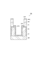
- FIG. 12A is a partial cross-sectional view of another example of the substrate to which the step STa is applied in the step ST1 of the method MT.
- FIG. 12B is a partial cross-sectional view of another example of the substrate to which the step STb is applied in the step ST1 of the method MT.
- FIG. 13 is a partial cross-sectional view of another example of the substrate to which the step ST1 of the method MT is applied.
- FIG. 14 is a partial cross-sectional view of another example of the substrate to which the step ST2 of the method MT is applied.
- FIG. 12A is a partial cross-sectional view of another example of the substrate to which the step STa is applied in the step ST1 of the method MT.
- FIG. 12B is a partial cross-sectional view of another example of the substrate to which the step STb is applied in the step ST1 of the method MT.
- FIG. 13 is a partial cross-sectional view of another example of the substrate to which the step ST1 of the
- FIG. 15A is a partial cross-sectional view of another example of the substrate to which the step STa is applied in the step ST3 of the method MT.
- FIG. 15B is a partial cross-sectional view of another example of the substrate to which the step STb is applied in the step ST3 of the method MT.
- FIG. 16 is a partial cross-sectional view of another example of the substrate to which the step ST3 of the method MT is applied.
- FIG. 11 shows the substrate WA in a state after the first region R1 is etched in the depth direction of the substrate W in the step ST1 and the step STa is further performed.
- step STa a deposit DPF is formed on the substrate WA, as shown in FIG.
- step STb the first region R1 is further etched by the fluorocarbon in the deposit DPF.
- the substrate WA is processed into a shape as shown in FIG. That is, in step ST1, the first region R1 is processed so as to have an upper surface at a deeper position in the substrate W than the second region R2.
- the first region R1 is also etched by the active species of fluorocarbon and / or the active species of fluorine applied to the substrate WA from the plasma of the processing gas containing the fluorocarbon gas. You may.
- step ST2 when step ST2 is performed, a deposit DPC is formed on the substrate WA, as shown in FIG. In FIG. 14, the deposit DPF that may be left on the substrate W after the end of the step ST1 is omitted.
- the process STa of the processing PE is performed in the subsequent process ST3
- a deposit DPF is formed on the substrate WA, as shown in FIG.
- the process STb is performed, as shown in FIG. 15B
- the first region R1 is further etched by the fluorocarbon in the deposit DPF.
- the substrate WA is processed into a shape as shown in FIG.
- the first region R1 is also etched by the active species of fluorocarbon and / or the active species of fluorine applied to the substrate WA from the plasma of the processing gas containing the fluorocarbon gas. You may.
- Step ST1, Step ST2, and Step ST3 may be performed using different plasma processing apparatuses.
- another plasma processing apparatus may be used as long as the plasma processing apparatus can form the above-described magnetic field.
- another plasma processing apparatus include a capacitively-coupled plasma processing apparatus different from the plasma processing apparatus 1, an inductively-coupled plasma processing apparatus, and a plasma processing apparatus that generates plasma using a surface wave such as a microwave. Is done.
- the above-described magnetic field formed in the chamber 10 by the electromagnet 60 in the step ST2 may be generated in the chamber 10 in another step in addition to the step ST2. That is, the magnetic field is applied to the chamber in at least one of the steps ST1, ST3, the step STa in the step ST1, the step STb in the step ST1, the step STa in the step ST3, and the step STb in the step ST3. 10 may be generated.
- step ST2 was performed on the sample substrate using the plasma processing apparatus 1.
- the conditions of step ST2 are as follows. ⁇ Condition of Step ST2> -Pressure in the chamber 10: 10 mTorr (1.333) Pa Gases supplied into the chamber 10: CH 4 gas (25 sccm) and Ar gas (250 sccm) -First high frequency power: 60 MHz, 300 W -Second high frequency power: 0W
- the thickness of the formed deposit was measured at each of 57 locations on two orthogonal diameters on the surface of the sample substrate, and the deposition rate of the deposit was determined from the thickness and the execution time of step ST2. . Then, the average value (nm / min) and the variation (%) of the deposition rates at 57 locations were obtained.
- the variation was calculated by the following equation (Max ⁇ Min) / (Average ⁇ 2) ⁇ 100
- Max is the maximum value of the 57 deposition rates
- Min is the minimum value of the 57 deposition rates
- Average is the average value of the deposition rates of the 57 locations.
- the average value and the variation of the deposition rate at 57 points were 21.2 nm / min and 2.0%, respectively.
- step ST2 it is possible to reduce the variation in the deposition rate of the deposit in the plane of the substrate. That is, it was confirmed that by forming a magnetic field in the chamber 10 using the electromagnet 60, it is possible to improve the in-plane uniformity of the deposition rate of the deposit on the substrate.
Landscapes
- Engineering & Computer Science (AREA)
- Physics & Mathematics (AREA)
- Chemical & Material Sciences (AREA)
- Plasma & Fusion (AREA)
- Analytical Chemistry (AREA)
- Power Engineering (AREA)
- Computer Hardware Design (AREA)
- Microelectronics & Electronic Packaging (AREA)
- Manufacturing & Machinery (AREA)
- Condensed Matter Physics & Semiconductors (AREA)
- General Physics & Mathematics (AREA)
- Chemical Kinetics & Catalysis (AREA)
- Inorganic Chemistry (AREA)
- General Chemical & Material Sciences (AREA)
- Electromagnetism (AREA)
- Spectroscopy & Molecular Physics (AREA)
- Drying Of Semiconductors (AREA)
- Plasma Technology (AREA)
- Manufacturing Of Printed Circuit Boards (AREA)
- Crystals, And After-Treatments Of Crystals (AREA)
Priority Applications (3)
| Application Number | Priority Date | Filing Date | Title |
|---|---|---|---|
| KR1020217007621A KR102767140B1 (ko) | 2018-08-24 | 2019-08-13 | 에칭하는 방법 및 플라즈마 처리 장치 |
| CN201980053944.6A CN112567502B (zh) | 2018-08-24 | 2019-08-13 | 蚀刻的方法和等离子体处理装置 |
| US17/270,499 US11710643B2 (en) | 2018-08-24 | 2019-08-13 | Method of etching and plasma processing apparatus |
Applications Claiming Priority (2)
| Application Number | Priority Date | Filing Date | Title |
|---|---|---|---|
| JP2018-157570 | 2018-08-24 | ||
| JP2018157570A JP7110034B2 (ja) | 2018-08-24 | 2018-08-24 | エッチングする方法及びプラズマ処理装置 |
Publications (1)
| Publication Number | Publication Date |
|---|---|
| WO2020040005A1 true WO2020040005A1 (ja) | 2020-02-27 |
Family
ID=69592629
Family Applications (1)
| Application Number | Title | Priority Date | Filing Date |
|---|---|---|---|
| PCT/JP2019/031859 Ceased WO2020040005A1 (ja) | 2018-08-24 | 2019-08-13 | エッチングする方法及びプラズマ処理装置 |
Country Status (6)
| Country | Link |
|---|---|
| US (1) | US11710643B2 (enExample) |
| JP (1) | JP7110034B2 (enExample) |
| KR (1) | KR102767140B1 (enExample) |
| CN (1) | CN112567502B (enExample) |
| TW (1) | TWI811432B (enExample) |
| WO (1) | WO2020040005A1 (enExample) |
Cited By (1)
| Publication number | Priority date | Publication date | Assignee | Title |
|---|---|---|---|---|
| WO2022059440A1 (ja) * | 2020-09-18 | 2022-03-24 | 東京エレクトロン株式会社 | エッチング方法、プラズマ処理装置、及び基板処理システム |
Families Citing this family (5)
| Publication number | Priority date | Publication date | Assignee | Title |
|---|---|---|---|---|
| JP7492928B2 (ja) * | 2021-02-10 | 2024-05-30 | 東京エレクトロン株式会社 | 基板支持器、プラズマ処理システム及びプラズマエッチング方法 |
| US12347645B2 (en) * | 2021-04-27 | 2025-07-01 | Tokyo Electron Limited | Substrate processing method and substrate processing apparatus |
| TWI828187B (zh) * | 2021-06-22 | 2024-01-01 | 日商東京威力科創股份有限公司 | 蝕刻方法及電漿處理裝置 |
| US12308250B2 (en) * | 2022-05-12 | 2025-05-20 | Tokyo Electron Limited | Pre-etch treatment for metal etch |
| CN119340234A (zh) * | 2023-07-20 | 2025-01-21 | 中微半导体设备(上海)股份有限公司 | 用于等离子体刻蚀的气体、气体组合、刻蚀方法及设备 |
Citations (6)
| Publication number | Priority date | Publication date | Assignee | Title |
|---|---|---|---|---|
| JPH09270416A (ja) * | 1996-03-29 | 1997-10-14 | Sony Corp | ドライエッチング装置およびドライエッチング方法 |
| JP2001053061A (ja) * | 1999-08-06 | 2001-02-23 | Hitachi Ltd | ドライエッチング方法 |
| JP2007284794A (ja) * | 2006-04-19 | 2007-11-01 | Maxim Integrated Products Inc | 膜の堆積/エッチング特性を変えるための磁気フィルタ装置を備えたプラズマ・システム |
| JP2013004679A (ja) * | 2011-06-15 | 2013-01-07 | Tokyo Electron Ltd | プラズマエッチング方法 |
| JP2017216284A (ja) * | 2016-05-30 | 2017-12-07 | 東京エレクトロン株式会社 | エッチング方法 |
| JP2018032720A (ja) * | 2016-08-24 | 2018-03-01 | 東京エレクトロン株式会社 | 基板処理方法 |
Family Cites Families (15)
| Publication number | Priority date | Publication date | Assignee | Title |
|---|---|---|---|---|
| EP0777267A1 (en) * | 1995-11-28 | 1997-06-04 | Applied Materials, Inc. | Oxide etch process with high selectivity to nitride suitable for use on surfaces of uneven topography |
| EP1334514A2 (en) * | 2000-11-01 | 2003-08-13 | Applied Materials, Inc. | Dielectric etch chamber with expanded process window |
| US7547635B2 (en) * | 2002-06-14 | 2009-06-16 | Lam Research Corporation | Process for etching dielectric films with improved resist and/or etch profile characteristics |
| JP4643916B2 (ja) * | 2004-03-02 | 2011-03-02 | 株式会社アルバック | 層間絶縁膜のドライエッチング方法及びその装置 |
| CN101681830B (zh) * | 2007-05-11 | 2014-03-12 | 爱发科股份有限公司 | 干式蚀刻装置及干式蚀刻方法 |
| JP5223377B2 (ja) * | 2008-02-29 | 2013-06-26 | 東京エレクトロン株式会社 | プラズマ処理装置用の電極、プラズマ処理装置及びプラズマ処理方法 |
| JP2010027175A (ja) * | 2008-07-23 | 2010-02-04 | Showa Denko HD Singapore Pte Ltd | 炭素膜の形成方法、磁気記録媒体の製造方法、及び炭素膜の形成装置 |
| US8664126B2 (en) * | 2011-06-10 | 2014-03-04 | Applied Materials, Inc. | Selective deposition of polymer films on bare silicon instead of oxide surface |
| JP6008771B2 (ja) * | 2013-01-21 | 2016-10-19 | 東京エレクトロン株式会社 | 多層膜をエッチングする方法 |
| KR20150055473A (ko) * | 2013-11-13 | 2015-05-21 | 삼성전자주식회사 | 탄소 함유 박막의 형성 방법 및 이를 이용한 반도체 소자의 제조 방법 |
| JP6396699B2 (ja) * | 2014-02-24 | 2018-09-26 | 東京エレクトロン株式会社 | エッチング方法 |
| JP6320282B2 (ja) * | 2014-12-05 | 2018-05-09 | 東京エレクトロン株式会社 | エッチング方法 |
| JP2016136606A (ja) * | 2015-01-16 | 2016-07-28 | 東京エレクトロン株式会社 | エッチング方法 |
| JP6438831B2 (ja) * | 2015-04-20 | 2018-12-19 | 東京エレクトロン株式会社 | 有機膜をエッチングする方法 |
| JP6851217B2 (ja) * | 2017-02-16 | 2021-03-31 | 東京エレクトロン株式会社 | プラズマ処理方法及びプラズマ処理装置 |
-
2018
- 2018-08-24 JP JP2018157570A patent/JP7110034B2/ja active Active
-
2019
- 2019-08-13 WO PCT/JP2019/031859 patent/WO2020040005A1/ja not_active Ceased
- 2019-08-13 US US17/270,499 patent/US11710643B2/en active Active
- 2019-08-13 CN CN201980053944.6A patent/CN112567502B/zh active Active
- 2019-08-13 KR KR1020217007621A patent/KR102767140B1/ko active Active
- 2019-08-22 TW TW108129968A patent/TWI811432B/zh active
Patent Citations (6)
| Publication number | Priority date | Publication date | Assignee | Title |
|---|---|---|---|---|
| JPH09270416A (ja) * | 1996-03-29 | 1997-10-14 | Sony Corp | ドライエッチング装置およびドライエッチング方法 |
| JP2001053061A (ja) * | 1999-08-06 | 2001-02-23 | Hitachi Ltd | ドライエッチング方法 |
| JP2007284794A (ja) * | 2006-04-19 | 2007-11-01 | Maxim Integrated Products Inc | 膜の堆積/エッチング特性を変えるための磁気フィルタ装置を備えたプラズマ・システム |
| JP2013004679A (ja) * | 2011-06-15 | 2013-01-07 | Tokyo Electron Ltd | プラズマエッチング方法 |
| JP2017216284A (ja) * | 2016-05-30 | 2017-12-07 | 東京エレクトロン株式会社 | エッチング方法 |
| JP2018032720A (ja) * | 2016-08-24 | 2018-03-01 | 東京エレクトロン株式会社 | 基板処理方法 |
Cited By (4)
| Publication number | Priority date | Publication date | Assignee | Title |
|---|---|---|---|---|
| WO2022059440A1 (ja) * | 2020-09-18 | 2022-03-24 | 東京エレクトロン株式会社 | エッチング方法、プラズマ処理装置、及び基板処理システム |
| CN114762091A (zh) * | 2020-09-18 | 2022-07-15 | 东京毅力科创株式会社 | 蚀刻方法、等离子体处理装置以及基板处理系统 |
| JP7123287B1 (ja) * | 2020-09-18 | 2022-08-22 | 東京エレクトロン株式会社 | エッチング方法、プラズマ処理装置、基板処理システム、及びプログラム |
| CN114762091B (zh) * | 2020-09-18 | 2023-12-15 | 东京毅力科创株式会社 | 蚀刻方法、等离子体处理装置、基板处理系统以及存储介质 |
Also Published As
| Publication number | Publication date |
|---|---|
| KR20210041072A (ko) | 2021-04-14 |
| US20210335623A1 (en) | 2021-10-28 |
| TW202027161A (zh) | 2020-07-16 |
| CN112567502B (zh) | 2024-08-20 |
| JP2020031190A (ja) | 2020-02-27 |
| US11710643B2 (en) | 2023-07-25 |
| CN112567502A (zh) | 2021-03-26 |
| TWI811432B (zh) | 2023-08-11 |
| KR102767140B1 (ko) | 2025-02-13 |
| JP7110034B2 (ja) | 2022-08-01 |
Similar Documents
| Publication | Publication Date | Title |
|---|---|---|
| KR102767140B1 (ko) | 에칭하는 방법 및 플라즈마 처리 장치 | |
| CN109559968B (zh) | 等离子体处理装置 | |
| CN115938906B (zh) | 等离子体处理装置 | |
| US20240290625A1 (en) | Plasma processing apparatus | |
| KR102723940B1 (ko) | 에칭 방법 | |
| JP2021150510A (ja) | エッチング方法及びプラズマ処理装置 |
Legal Events
| Date | Code | Title | Description |
|---|---|---|---|
| 121 | Ep: the epo has been informed by wipo that ep was designated in this application |
Ref document number: 19851520 Country of ref document: EP Kind code of ref document: A1 |
|
| NENP | Non-entry into the national phase |
Ref country code: DE |
|
| 122 | Ep: pct application non-entry in european phase |
Ref document number: 19851520 Country of ref document: EP Kind code of ref document: A1 |