WO2020031635A1 - スパッタリングターゲット - Google Patents
スパッタリングターゲット Download PDFInfo
- Publication number
- WO2020031635A1 WO2020031635A1 PCT/JP2019/028053 JP2019028053W WO2020031635A1 WO 2020031635 A1 WO2020031635 A1 WO 2020031635A1 JP 2019028053 W JP2019028053 W JP 2019028053W WO 2020031635 A1 WO2020031635 A1 WO 2020031635A1
- Authority
- WO
- WIPO (PCT)
- Prior art keywords
- sputtering target
- sputtering
- mol
- target according
- present
- Prior art date
- Legal status (The legal status is an assumption and is not a legal conclusion. Google has not performed a legal analysis and makes no representation as to the accuracy of the status listed.)
- Ceased
Links
Images

Classifications
-
- C—CHEMISTRY; METALLURGY
- C23—COATING METALLIC MATERIAL; COATING MATERIAL WITH METALLIC MATERIAL; CHEMICAL SURFACE TREATMENT; DIFFUSION TREATMENT OF METALLIC MATERIAL; COATING BY VACUUM EVAPORATION, BY SPUTTERING, BY ION IMPLANTATION OR BY CHEMICAL VAPOUR DEPOSITION, IN GENERAL; INHIBITING CORROSION OF METALLIC MATERIAL OR INCRUSTATION IN GENERAL
- C23C—COATING METALLIC MATERIAL; COATING MATERIAL WITH METALLIC MATERIAL; SURFACE TREATMENT OF METALLIC MATERIAL BY DIFFUSION INTO THE SURFACE, BY CHEMICAL CONVERSION OR SUBSTITUTION; COATING BY VACUUM EVAPORATION, BY SPUTTERING, BY ION IMPLANTATION OR BY CHEMICAL VAPOUR DEPOSITION, IN GENERAL
- C23C14/00—Coating by vacuum evaporation, by sputtering or by ion implantation of the coating forming material
- C23C14/22—Coating by vacuum evaporation, by sputtering or by ion implantation of the coating forming material characterised by the process of coating
- C23C14/34—Sputtering
- C23C14/3407—Cathode assembly for sputtering apparatus, e.g. Target
- C23C14/3414—Metallurgical or chemical aspects of target preparation, e.g. casting, powder metallurgy
-
- C—CHEMISTRY; METALLURGY
- C04—CEMENTS; CONCRETE; ARTIFICIAL STONE; CERAMICS; REFRACTORIES
- C04B—LIME, MAGNESIA; SLAG; CEMENTS; COMPOSITIONS THEREOF, e.g. MORTARS, CONCRETE OR LIKE BUILDING MATERIALS; ARTIFICIAL STONE; CERAMICS; REFRACTORIES; TREATMENT OF NATURAL STONE
- C04B35/00—Shaped ceramic products characterised by their composition; Ceramics compositions; Processing powders of inorganic compounds preparatory to the manufacturing of ceramic products
- C04B35/01—Shaped ceramic products characterised by their composition; Ceramics compositions; Processing powders of inorganic compounds preparatory to the manufacturing of ceramic products based on oxide ceramics
- C04B35/453—Shaped ceramic products characterised by their composition; Ceramics compositions; Processing powders of inorganic compounds preparatory to the manufacturing of ceramic products based on oxide ceramics based on zinc, tin, or bismuth oxides or solid solutions thereof with other oxides, e.g. zincates, stannates or bismuthates
-
- C—CHEMISTRY; METALLURGY
- C23—COATING METALLIC MATERIAL; COATING MATERIAL WITH METALLIC MATERIAL; CHEMICAL SURFACE TREATMENT; DIFFUSION TREATMENT OF METALLIC MATERIAL; COATING BY VACUUM EVAPORATION, BY SPUTTERING, BY ION IMPLANTATION OR BY CHEMICAL VAPOUR DEPOSITION, IN GENERAL; INHIBITING CORROSION OF METALLIC MATERIAL OR INCRUSTATION IN GENERAL
- C23C—COATING METALLIC MATERIAL; COATING MATERIAL WITH METALLIC MATERIAL; SURFACE TREATMENT OF METALLIC MATERIAL BY DIFFUSION INTO THE SURFACE, BY CHEMICAL CONVERSION OR SUBSTITUTION; COATING BY VACUUM EVAPORATION, BY SPUTTERING, BY ION IMPLANTATION OR BY CHEMICAL VAPOUR DEPOSITION, IN GENERAL
- C23C14/00—Coating by vacuum evaporation, by sputtering or by ion implantation of the coating forming material
- C23C14/06—Coating by vacuum evaporation, by sputtering or by ion implantation of the coating forming material characterised by the coating material
- C23C14/08—Oxides
- C23C14/086—Oxides of zinc, germanium, cadmium, indium, tin, thallium or bismuth
-
- G—PHYSICS
- G11—INFORMATION STORAGE
- G11B—INFORMATION STORAGE BASED ON RELATIVE MOVEMENT BETWEEN RECORD CARRIER AND TRANSDUCER
- G11B7/00—Recording or reproducing by optical means, e.g. recording using a thermal beam of optical radiation by modifying optical properties or the physical structure, reproducing using an optical beam at lower power by sensing optical properties; Record carriers therefor
- G11B7/24—Record carriers characterised by shape, structure or physical properties, or by the selection of the material
- G11B7/241—Record carriers characterised by shape, structure or physical properties, or by the selection of the material characterised by the selection of the material
- G11B7/252—Record carriers characterised by shape, structure or physical properties, or by the selection of the material characterised by the selection of the material of layers other than recording layers
- G11B7/257—Record carriers characterised by shape, structure or physical properties, or by the selection of the material characterised by the selection of the material of layers other than recording layers of layers having properties involved in recording or reproduction, e.g. optical interference layers or sensitising layers or dielectric layers, which are protecting the recording layers
- G11B7/2578—Record carriers characterised by shape, structure or physical properties, or by the selection of the material characterised by the selection of the material of layers other than recording layers of layers having properties involved in recording or reproduction, e.g. optical interference layers or sensitising layers or dielectric layers, which are protecting the recording layers consisting essentially of inorganic materials
-
- G—PHYSICS
- G11—INFORMATION STORAGE
- G11B—INFORMATION STORAGE BASED ON RELATIVE MOVEMENT BETWEEN RECORD CARRIER AND TRANSDUCER
- G11B7/00—Recording or reproducing by optical means, e.g. recording using a thermal beam of optical radiation by modifying optical properties or the physical structure, reproducing using an optical beam at lower power by sensing optical properties; Record carriers therefor
- G11B7/24—Record carriers characterised by shape, structure or physical properties, or by the selection of the material
- G11B7/26—Apparatus or processes specially adapted for the manufacture of record carriers
Definitions
- the present invention relates to a sputtering target. More specifically, the present invention relates to a sputtering target for forming a protective film on an optical recording medium.
- optical information recording media are broadly classified into rewritable types such as BD-RE and write-once types such as BD-R.
- the optical information recording medium has a laminated structure having a protective layer composed of a dielectric layer above and below the recording layer, and a ZnS-SiO 2 material is used as the protective layer (Patent Reference 1).
- the ZnS-based dielectric layer has a problem in that S (sulfur component) diffuses into the recording layer, thereby deteriorating recording performance.
- a sputtering target containing ZrO 2 as a main component has been proposed for the purpose of forming a protective layer containing no sulfide (see Patent Document 2).
- the ZrO 2 -based target changes its crystal structure due to heat and changes its volume, cracks are generated in the target when a film is formed by repeated heating for a long time at a high output.
- Patent Document 3 As another type of protective layer, an In 2 O 3 -based material has been proposed (see Patent Document 3). However, In 2 O 3 is suspected of being carcinogenic, and reductions or alternative materials are being sought.
- the present invention has been made in view of the above-described background art, and its purpose is to reduce the risk of human body, and even when performing high-power and long-time sputtering, the generation of cracks. It is to provide a sputtering target that can be suppressed.
- the present inventors have conducted intensive studies on a sputtering target that does not use sulfur, suppresses the content of Zr, and has little danger to the human body. As a result, the present inventors have found that the above object can be solved by using a sputtering target in which Zn is contained as a main component, a specific metal containing Zr is contained in a specific composition, and Zr is a composite oxide. Was completed.
- the present invention includes Zn, Sn, Zr, and O, the content of Zn is 30 to 60 mol% based on the whole metal component, and the content of Zr is 10 to 40 mol% based on the whole metal component.
- % which is a sputtering target containing a composite oxide of Zr.
- the sputtering target may have a maximum peak at a diffraction angle (2 ⁇ ) of around 28 ° in X-ray diffraction measurement using CuK ⁇ radiation.
- the sputtering target may have a Sn content of 10 to 30 mol% based on the entire metal component.
- the sputtering target may not contain In.
- the composite oxide may contain Zn and Zr.
- the sputtering target may further include a composite oxide containing Zn and Sn.
- the sputtering target may further include at least one selected from the group consisting of Y, Mg, and Ca.
- the sputtering target may further contain Si.
- the sputtering target may further contain Ga and / or Al.
- the sputtering target may have a resistance value of 10 ⁇ ⁇ cm or less.
- the sputtering target may be for forming a protective film on an optical recording medium.
- the sputtering target of the present invention has a low risk to the human body, and is a target in which cracks are suppressed even when high-power and long-time sputtering is performed.
- a simple oxide does not have conductivity, and it is difficult to perform sputtering by direct current (DC).
- DC direct current
- the sputtering target of the present invention has conductivity, DC sputtering can be performed.
- the sputtering target of the present invention has a small specific resistance, it is a very useful target in terms of film productivity.
- Example 3 is an X-ray diffraction pattern of the sputtering targets of Example 1 and Comparative Example 1.
- the sputtering target of the present invention contains Zn, Sn, Zr, and O, the content of Zn is 30 to 60 mol% based on the entire metal component, and the content of Zr is 10% based on the entire metal component. To 40 mol%, and contains a complex oxide of Zr.
- the sputtering target of the present invention contains Zn, Sn, Zr, and O as essential components. By including all of Zn, Sn, Zr, and O as essential components, the characteristics of a film obtained by sputtering can be satisfied.
- the sputtering target of the present invention does not contain In. In forms oxides that are dangerous to the human body. By not containing In, a highly safe sputtering target can be obtained.
- the sputtering target of the present invention preferably does not contain S.
- S sulfur component
- S is a substance that diffuses into the recording layer and causes a decrease in recording performance.
- the sputtering target of the present invention preferably further contains at least one selected from the group consisting of Y, Mg, and Ca. Furthermore, when at least one selected from the group consisting of Y, Mg, and Ca is included, it is possible to suppress a change in volume of Zr that does not form a composite oxide due to heat, and to further improve crack resistance. Becomes
- the sputtering target of the present invention preferably further contains Si. Further, when Si is included, it is possible to further improve the crack resistance.
- the sputtering target of the present invention further contains Ga and / or Al. Furthermore, when Ga and / or Al is included, the resistance value of the target can be further reduced, and abnormal discharge during DC sputtering can be further reduced, and crack resistance can be further improved.
- Zr which is an essential component, forms a composite oxide with another metal.
- ZrO 2 which is a simple oxide of Zr, changes its crystal structure due to heat and changes its volume, when a film is formed by repeated heating for a long time at a high output, a crack is generated in the target.
- the sputtering target of the present invention can suppress the occurrence of cracks by containing the Zr composite oxide.
- the sputtering target of the present invention has conductivity due to the presence of the composite oxide. For this reason, a single oxide does not have conductivity, and direct-current (DC) sputtering is difficult. According to the sputtering target of the present invention, DC sputtering can be performed.
- DC sputtering has a higher film formation rate and higher sputtering efficiency than, for example, RF sputtering.
- the DC sputtering apparatus is inexpensive, easy to control, and consumes less power.
- a layer having a small thickness can be formed. Therefore, the sputtering target of the present invention is a very useful target in terms of film productivity.
- the Zr composite oxide can be formed by heat-treating the ZrO 2 powder and the ZnO powder.
- the sputtering target of the present invention has a maximum peak at a diffraction angle (2 ⁇ ) of around 28 ° in X-ray diffraction measurement using CuK ⁇ radiation. In the vicinity where the diffraction angle (2 ⁇ ) becomes 28 °, a composite oxide of Zr and Zn appears.
- the composite oxide formed by Zr preferably contains Zn and Zr.
- the composite oxide containing Zn and Zr for example, ZnZrO 3.
- the sputtering target of the present invention preferably further contains a composite oxide containing Zn and Sn.
- a composite oxide containing Zn and Sn for example, Zn 2 SnO 4 is given.
- the content of Zn is in the range of 30 to 60 mol% based on the entire metal component. It is preferably in the range of 40 to 60 mol%, and more preferably in the range of 45 to 55 mol%.
- the content of Zr is in the range of 10 to 40 mol% based on the entire metal component. It is preferably in the range of 15 to 35 mol%, more preferably in the range of 20 to 30 mol%.
- the content of Sn is preferably in the range of 10 to 30 mol% with respect to the entire metal component.
- the range is more preferably from 18 to 27 mol%, particularly preferably from 20 to 25 mol%.
- the sputtering target of the present invention preferably has a resistance value of 10 ⁇ ⁇ cm or less.
- the resistance value is more preferably 5 ⁇ ⁇ cm or less, and particularly preferably 1 ⁇ ⁇ cm or less.
- the resistance value is 10 ⁇ ⁇ cm or less, DC sputtering can be performed without abnormal discharge.
- the sputtering target of the present invention preferably has a relative density ratio of 90% or more.
- the relative density ratio is more preferably at least 95%, particularly preferably at least 97%.
- a method of improving the relative density of the sputtering target for example, a method of increasing the sintering pressure at the time of manufacturing the sputtering target may be mentioned.
- the sputtering target of the present invention is preferably a target for forming a protective film of an optical recording medium.
- ADVANTAGE OF THE INVENTION According to this invention, the danger to a human body is small, Moreover, even when performing high-power and long-time sputtering, generation
- the method for manufacturing the sputtering target of the present invention is not particularly limited, and a known method implemented in this technical field can be applied.
- an oxide powder containing each metal element is wet-mixed, and the obtained mixed powder is sintered at a high temperature and a high pressure by a hot press or the like.
- a HIP method hot isostatic pressing sintering method or the like may be employed.
- weighed raw material powders, ethanol having a mass 1 times the mass of the mass of the raw material powders, and zirconia balls (diameter 5 mm) having a mass 0.5 times as much as the total mass of the raw material powders were charged.
- Wet mixing was performed for 20 hours.
- the slurry solution containing the mixed raw material powders was filtered using a sieve having a mesh size of 2 mm to separate zirconia balls.
- the obtained slurry solution was dried by heating, and crushed using a sieve having openings of 250 ⁇ m to obtain a mixed powder.
- the obtained mixed powder was filled in a carbon mold, and hot pressing (high-temperature high-pressure pressing) was performed in an argon atmosphere at a sintering temperature of 950 ° C., a sintering pressure of 400 kgf / cm 2 , and a sintering time of 2 hours. After hot pressing, the obtained sintered body was machined to produce a sputtering target.
- FIG. 1 shows the obtained diffraction pattern. As shown in FIG. 1, a maximum peak is observed near a diffraction angle (2 ⁇ ) of 28 °, and this peak is a peak that appears due to the formation of ZnZrO 3 .
- the obtained sputtering target was bonded to a copper backing plate using In solder. This was attached to an ordinary DC sputtering apparatus, and after evacuation was performed to 1 ⁇ 10 ⁇ 4 Pa or less, Ar gas and O 2 gas were introduced, and the internal pressure of the apparatus was set to 0.3 Pa. At this time, the partial pressure of oxygen (O 2 / Ar + O 2 ) was set to 70%. A power of 12 W / cm 2 was applied from a DC power supply, and sputtering was performed for 60 minutes. As a result, cracks did not occur during sputtering, and a stable film could be formed.
- Example 3> A sputtering target was prepared and evaluated in the same manner as in Example 1 except that the ratio of each contained metal was changed using ZnO powder, SnO 2 powder, and ZrO 2 powder as shown in Table 1. Table 1 shows the evaluation results.
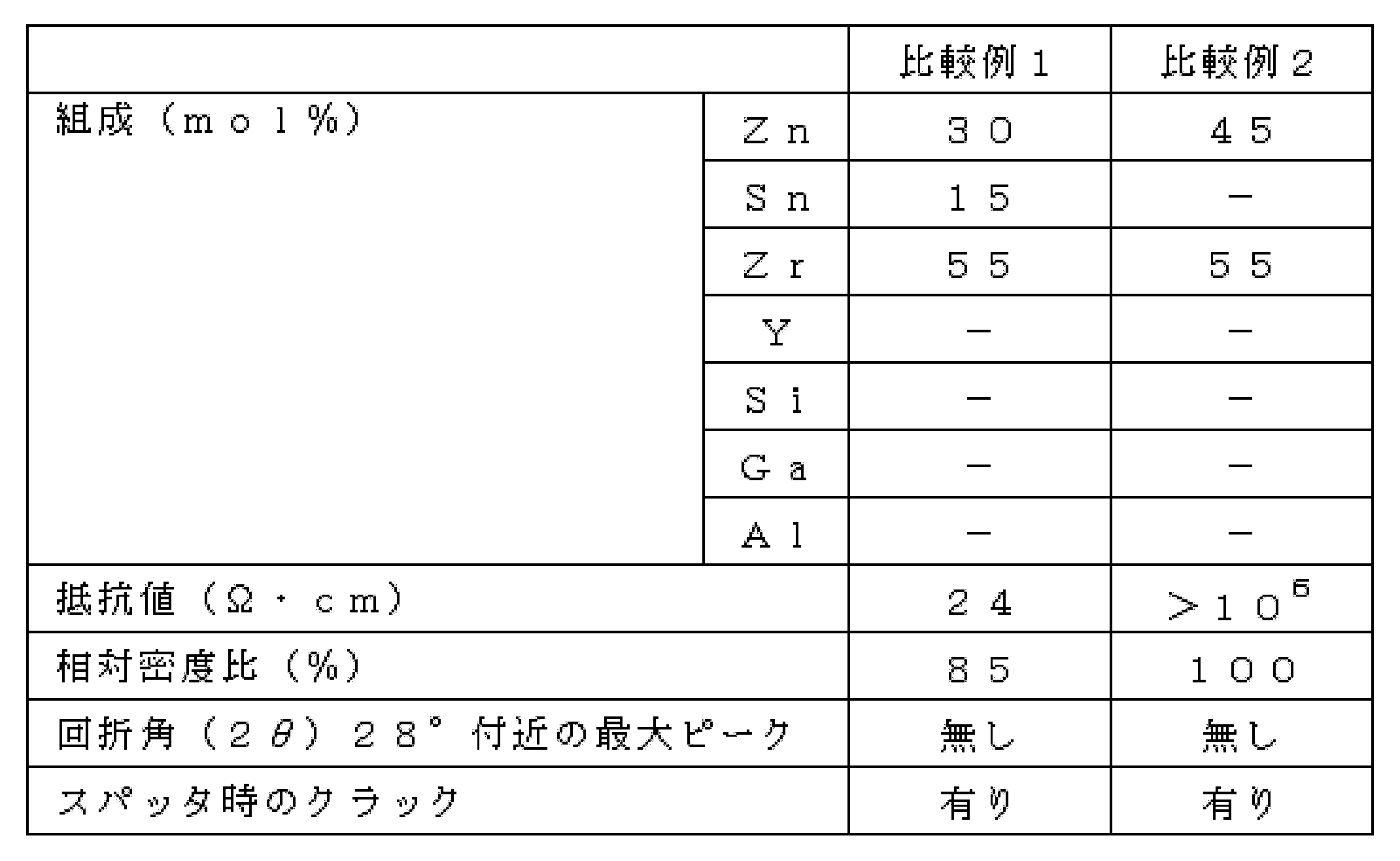
- Example 1 A sputtering target was prepared and evaluated in the same manner as in Example 1, except that the ratio of each contained metal was changed using ZnO powder, SnO 2 powder, and ZrO 2 powder as shown in Table 2.
- FIG. 1 shows an X-ray diffraction pattern by CuK ⁇ ray
- Table 2 shows the evaluation results.
- ⁇ Comparative Example 2> ZnO powder (purity: 99.9% or more, average particle size: 2 ⁇ m) and ZrO 2 powder (purity: 99.9% or more, average particle size: 0.5 ⁇ m) were prepared by mixing Zn: Zr 45: 55 (atomic%).
Landscapes
- Chemical & Material Sciences (AREA)
- Engineering & Computer Science (AREA)
- Organic Chemistry (AREA)
- Materials Engineering (AREA)
- Mechanical Engineering (AREA)
- Metallurgy (AREA)
- Chemical Kinetics & Catalysis (AREA)
- Manufacturing & Machinery (AREA)
- Ceramic Engineering (AREA)
- Inorganic Chemistry (AREA)
- Structural Engineering (AREA)
- Physical Vapour Deposition (AREA)
- Optical Record Carriers And Manufacture Thereof (AREA)
- Manufacturing Optical Record Carriers (AREA)
Abstract
人体への危険性が少なく、また、高出力で長時間のスパッタリングを実施した場合であっても、クラックの発生を抑制できるスパッタリングターゲットを提供する。 Zn、Sn、Zr、およびOを含み、Znの含有量は、金属成分全体に対して30~60mol%であり、Zrの含有量は、金属成分全体に対して10~40mol%であり、Zrの複合酸化物を含む、スパッタリングターゲットとする。
Description
本発明は、スパッタリングターゲットに関する。さらに詳しくは、光記録媒体の保護膜形成用スパッタリングターゲットに関する。
近年、テレビのハイビジョン化や、クラウドコンピューティングといったネットワークの発達、PCで取り扱うデータ量の増大に伴い、大容量な光情報記録媒体(光ディスク)の開発および製品化が行われている。記録可能な光記録媒体としては、BD-REなどの書き換え型と、BD-Rなどの追記型に大別される。
ここで、光情報記録媒体は、記録層の上下に誘電体層からなる保護層を有する積層体構造となっており、保護層としては、ZnS-SiO2系の材料が使用されている(特許文献1参照)。しかしながら、ZnS系の誘電体層は、S(硫黄成分)が記録層中に拡散してしまい、記録性能を低下させる問題があった。
そこで、硫化物を含まない保護層を形成すること目的として、ZrO2を主成分とするスパッタリングターゲットが提案されている(特許文献2参照)。しかしながら、ZrO2系ターゲットは、熱により結晶構造が変化して体積変化を起こすため、高出力で長時間の繰り返し加熱による成膜を行うと、ターゲットにクラックが発生していた。
また別のタイプの保護層としては、In2O3系の材料が提案されている(特許文献3参照)。しかしながら、In2O3は発がん性が疑われており、削減、または代替材料が模索されている。
本発明は上記の背景技術に鑑みてなされたものであり、その目的は、人体への危険性が少なく、また、高出力で長時間のスパッタリングを実施した場合であっても、クラックの発生を抑制できるスパッタリングターゲットを提供することにある。
本発明者は、硫黄を用いることなく、また、Zrの含有量を抑制し、さらに、人体への危険性の少ないスパッタリングターゲットについて、鋭意検討を行った。その結果、Znを主成分として含有し、Zrを含む特定の金属を特定の組成で含み、Zrが複合酸化物を構成しているスパッタリングターゲットとすれば、上記課題を解決できることを見出し、本発明を完成させるに至った。
すなわち本発明は、Zn、Sn、Zr、およびOを含み、Znの含有量は、金属成分全体に対して30~60mol%であり、Zrの含有量は、金属成分全体に対して10~40mol%であり、Zrの複合酸化物を含む、スパッタリングターゲットである。
前記スパッタリングターゲットは、CuKα線によるX線回折測定において、回折角(2θ)が28°付近に最大ピークを有していてもよい。
前記スパッタリングターゲットは、Snの含有量が、金属成分全体に対して10~30mol%であってもよい。
前記スパッタリングターゲットは、Inを含んでいなくてもよい。
前記複合酸化物は、ZnとZrを含んでいてもよい。
前記スパッタリングターゲットは、さらに、ZnとSnを含む複合酸化物を含んでいてもよい。
前記スパッタリングターゲットは、さらに、Y、Mg、およびCaからなる群より選ばれる少なくとも1種を含んでいてもよい。
前記スパッタリングターゲットは、さらに、Siを含んでいてもよい。
前記スパッタリングターゲットは、さらに、Gaおよび/またはAlを含んでいてもよい。
前記スパッタリングターゲットは、抵抗値が10Ω・cm以下であってもよい。
前記スパッタリングターゲットは、光記録媒体の保護膜形成用であってもよい。
本発明のスパッタリングターゲットは、人体への危険性が少なく、また、高出力で長時間のスパッタリングを実施した場合であっても、クラックの発生が抑制されたターゲットとなる。
また、単体の酸化物は導電性を有さず、そのため直流(DC)によるスパッタリングが困難であったところ、本発明のスパッタリングターゲットは導電性を有するため、DCスパッタリングが可能となる。加えて、本発明のスパッタリングターゲットは、比抵抗値が小さいため、膜の生産性の点で大変有益なターゲットとなる。
以下、本発明の実施形態について説明する。
<スパッタリングターゲット>
本発明のスパッタリングターゲットは、Zn、Sn、Zr、およびOを含み、Znの含有量は、金属成分全体に対して30~60mol%であり、Zrの含有量は、金属成分全体に対して10~40mol%であり、Zrの複合酸化物を含むことを特徴とする。
本発明のスパッタリングターゲットは、Zn、Sn、Zr、およびOを含み、Znの含有量は、金属成分全体に対して30~60mol%であり、Zrの含有量は、金属成分全体に対して10~40mol%であり、Zrの複合酸化物を含むことを特徴とする。
[成分]
本発明のスパッタリングターゲットは、Zn、Sn、Zr、およびOを、必須の成分として含む。必須の成分として、Zn、Sn、Zr、およびOの全てを含むことにより、スパッタリングして得られる膜の特性を満足させることができる。
本発明のスパッタリングターゲットは、Zn、Sn、Zr、およびOを、必須の成分として含む。必須の成分として、Zn、Sn、Zr、およびOの全てを含むことにより、スパッタリングして得られる膜の特性を満足させることができる。
本発明のスパッタリングターゲットは、Inを含まないことが好ましい。Inは、人体にとって危険性のある酸化物を形成するため。Inを含有しないことにより、安全性の高いスパッタリングターゲットとなる。
また、本発明のスパッタリングターゲットは、Sを含まないことが好ましい。S(硫黄成分)は、記録層中に拡散し、記録性能を低下させる原因となる物質である。スパッタリングターゲットにSを含有させないことで、最終的に得られる光情報記録媒体の記録性能の低下を抑制することができる。
本発明のスパッタリングターゲットは、さらに、Y、Mg、およびCaからなる群より選ばれる少なくとも1種を含むことが好ましい。さらに、Y、Mg、およびCaからなる群より選ばれる少なくとも1種を含む場合には、複合酸化物を形成していないZrの熱による体積変化を抑制し、耐クラック性をより向上すること可能となる。
本発明のスパッタリングターゲットは、さらに、Siを含むことが好ましい。さらにSiを含む場合には、耐クラック性をより向上させることが可能となる。
本発明のスパッタリングターゲットは、さらに、Gaおよび/またはAlを含むことが好ましい。さらに、Gaおよび/またはAlを含む場合には、ターゲットの抵抗値をより低くすることができ、DCスパッタ時の異常放電をより減少させるとともに、耐クラック性をより向上させることが可能となる。
[複合酸化物]
本発明のスパッタリングターゲットは、必須成分であるZrが、他の金属との複合酸化物を形成している。ここで、Zrの単体酸化物であるZrO2は、熱により結晶構造が変化して体積変化を起こすため、高出力で長時間の繰り返し加熱による成膜を行うと、ターゲットにクラックを発生させる。これに対して本発明のスパッタリングターゲットは、Zrの複合酸化物が含まれていることで、クラックの発生を抑制することができる。
本発明のスパッタリングターゲットは、必須成分であるZrが、他の金属との複合酸化物を形成している。ここで、Zrの単体酸化物であるZrO2は、熱により結晶構造が変化して体積変化を起こすため、高出力で長時間の繰り返し加熱による成膜を行うと、ターゲットにクラックを発生させる。これに対して本発明のスパッタリングターゲットは、Zrの複合酸化物が含まれていることで、クラックの発生を抑制することができる。
また、本発明のスパッタリングターゲットは、複合酸化物の存在により、導電性を有する。このため、単体の酸化物では導電性を有さず、直流(DC)によるスパッタリングが困難であったところ、本発明のスパッタリングターゲットによれば、DCスパッタリングが可能となる。
DCスパッタリングは、例えばRFスパッタリングと比較して、成膜速度が速く、スパッタリング効率がよい。また、DCスパッタリング装置は、安価であり、制御が容易である上、電力の消費量も少ない。さらに、DCスパッタリングによれば、薄い膜厚の層を形成することも可能となる。したがって、本発明のスパッタリングターゲットは、膜の生産性の点で大変有益なターゲットとなる。
なお、Zrの複合酸化物は、ZrO2粉末とZnO粉末を熱処理することで、形成することができる。
(ピーク)
本発明のスパッタリングターゲットは、CuKα線によるX線回折測定において、回折角(2θ)が28°付近に最大ピークを有する。回折角(2θ)が28°となる付近には、ZrとZnとの複合酸化物が出現する。
本発明のスパッタリングターゲットは、CuKα線によるX線回折測定において、回折角(2θ)が28°付近に最大ピークを有する。回折角(2θ)が28°となる付近には、ZrとZnとの複合酸化物が出現する。
(複合酸化物の構成金属)
Zrが形成する複合酸化物は、ZnとZrを含むことが好ましい。ZnとZrを含む複合酸化物としては、例えば、ZnZrO3が挙げられる。
Zrが形成する複合酸化物は、ZnとZrを含むことが好ましい。ZnとZrを含む複合酸化物としては、例えば、ZnZrO3が挙げられる。
また、本発明のスパッタリングターゲットは、さらに、ZnとSnを含む複合酸化物を含むことが好ましい。ZnとSnを含む複合酸化物としては、例えば、Zn2SnO4が挙げられる。
[ターゲットの組成]
本発明のスパッタリングターゲットにおいて、Znの含有量は、金属成分全体に対して30~60mol%の範囲である。40~60mol%の範囲であることが好ましく、45~55mol%の範囲であることがさらに好ましい。
本発明のスパッタリングターゲットにおいて、Znの含有量は、金属成分全体に対して30~60mol%の範囲である。40~60mol%の範囲であることが好ましく、45~55mol%の範囲であることがさらに好ましい。
Znの含有量が、金属成分全体に対して30モル%未満の場合には、導電性付与効果が小さくなり、一方、60モル%を超える場合には、ターゲットを構成する他の金属成分の割合が小さくなることから、所望の特性の膜を得ることが困難となる。
本発明のスパッタリングターゲットにおいて、Zrの含有量は、金属成分全体に対して10~40mol%の範囲である。15~35mol%の範囲であることが好ましく、20~30mol%の範囲であることがさらに好ましい。
Zrの含有量が、金属成分全体に対して10モル%未満の場合には、所望の特性の膜を得ることが困難となり、一方、40モル%を超える場合には、DCスパッタ時に熱によるクラックが発生しやすくなるため好ましくない。
本発明のスパッタリングターゲットにおいて、Snの含有量は、金属成分全体に対して10~30mol%の範囲とすることが好ましい。18~27mol%の範囲であることがさらに好ましく、20~25mol%の範囲であることが特に好ましい。
Snの含有量が、金属成分全体に対して10モル%未満の場合には、導電性付与効果が小さくなり、一方、30モル%を超える場合には、焼結性が低下するため、得られるターゲットの密度が低下し、異常放電が生じやすくなるため好ましくない。
[抵抗値]
本発明のスパッタリングターゲットは、抵抗値が10Ω・cm以下であることが好ましい。抵抗値は、5Ω・cm以下であることがさらに好ましく、1Ω・cm以下であることが特に好ましい。
本発明のスパッタリングターゲットは、抵抗値が10Ω・cm以下であることが好ましい。抵抗値は、5Ω・cm以下であることがさらに好ましく、1Ω・cm以下であることが特に好ましい。
抵抗値が10Ω・cm以下であれば、DCスパッタリングを、異常放電なく実施することが可能となる。
[相対密度比]
本発明のスパッタリングターゲットは、相対密度比が90%以上であることが好ましい。相対密度比は、95%以上であることがさらに好ましく、97%以上であることが特に好ましい。
本発明のスパッタリングターゲットは、相対密度比が90%以上であることが好ましい。相対密度比は、95%以上であることがさらに好ましく、97%以上であることが特に好ましい。
相対密度比が90%以上であれば、スパッタ膜の均一性が高まるとともに、スパッタリング時のパーティクルの発生を抑制できることから、クラックの発生を抑制することができる。
なお、スパッタリングターゲットの相対密度を向上させる方法としては、例えば、スパッタリングターゲット製造時に、焼結圧力を高くする方法が挙げられる。
[用途]
本発明のスパッタリングターゲットは、光記録媒体の保護膜形成用ターゲットであることが好ましい。本発明によれば、人体への危険性が少なく、また、高出力で長時間のスパッタリングを実施した場合であっても、ターゲットへのクラックの発生を抑制でき、また、DCスパッタリングが可能であるため、光記録媒体の保護膜を生産性よく製造することができる。
本発明のスパッタリングターゲットは、光記録媒体の保護膜形成用ターゲットであることが好ましい。本発明によれば、人体への危険性が少なく、また、高出力で長時間のスパッタリングを実施した場合であっても、ターゲットへのクラックの発生を抑制でき、また、DCスパッタリングが可能であるため、光記録媒体の保護膜を生産性よく製造することができる。
<スパッタリングターゲットの製造方法>
本発明のスパッタリングターゲットの製造方法は、特に限定されるものではなく、本技術分野において実施されている、公知の方法を適用することができる。
本発明のスパッタリングターゲットの製造方法は、特に限定されるものではなく、本技術分野において実施されている、公知の方法を適用することができる。
例えば、各金属元素を含む酸化物の粉末を湿式混合し、得られた混合粉末を、高温高圧にてホットプレス等にて焼結する方法が挙げられる。あるいは、HIP法(熱間等方加圧式焼結法)等を採用してもよい。
次に、本発明の実施例等について説明するが、本発明はこれら実施例等に限定されるものではない。
<実施例1>
[スパッタリングターゲットの作製]
ZnO粉末(純度:99.9%以上、平均粒径:2μm)、SnO2粉末(純度:99.9%以上、平均粒径:1μm)、およびZrO2粉末(純度:99.9%以上、平均粒径:0.5μm)を、各含有金属の割合がZn:Zr:Sn=50:25:25(原子%)の割合となるように秤量した。
[スパッタリングターゲットの作製]
ZnO粉末(純度:99.9%以上、平均粒径:2μm)、SnO2粉末(純度:99.9%以上、平均粒径:1μm)、およびZrO2粉末(純度:99.9%以上、平均粒径:0.5μm)を、各含有金属の割合がZn:Zr:Sn=50:25:25(原子%)の割合となるように秤量した。
ナイロン容器に、秤量した各原料粉末と、各原料粉末の質量の合計に対して1倍の質量のエタノールと、0.5倍の質量のジルコニアボール(直径5mm)を投入し、ボールミル法により、20時間の湿式混合を行った。混合した各原材料粉末を含んだスラリー溶液を、目開き2mmの篩を使用して濾過し、ジルコニアボールを分離した。得られたスラリー溶液を加熱乾燥し、目開き250μmの篩いを用いて解砕することで、混合粉末を得た。
得られた混合粉末をカーボン製の型に充填し、アルゴン雰囲気中、焼結温度950℃、焼結圧力400kgf/cm2、焼結時間2時間として、ホットプレス(高温高圧プレス)を行った。ホットプレス後、得られた焼結体を機械加工し、スパッタリングターゲットを作製した。
[抵抗値の測定]
得られたスパッタリングターゲットについて、抵抗率計(株式会社三菱化学アナリテック製、MCP-T610)を用いて、抵抗値を測定した。結果を表1に示す。
得られたスパッタリングターゲットについて、抵抗率計(株式会社三菱化学アナリテック製、MCP-T610)を用いて、抵抗値を測定した。結果を表1に示す。
[相対密度比]
得られたスパッタリングターゲットについて、以下に記載する理論密度に対するターゲットの実測密度を比率で求め、相対密度比とした。
理論密度:使用する原材料それぞれについて重量配合比を比重で割った値を求め、その総和の逆数を取ったものとする。
得られたスパッタリングターゲットについて、以下に記載する理論密度に対するターゲットの実測密度を比率で求め、相対密度比とした。
理論密度:使用する原材料それぞれについて重量配合比を比重で割った値を求め、その総和の逆数を取ったものとする。
[Zr複合酸化物の確認]
得られたスパッタリングターゲットについて、株式会社リガク社製、多目的X線回折装置を用いて、CuKα線によるX線回折分析を実施した。得られた回折パターンを、図1に示す。図1に示されるように、回折角(2θ)が28°となる付近に最大ピークが認められ、このピークは、ZnZrO3の形成に起因して出現したピークである。
得られたスパッタリングターゲットについて、株式会社リガク社製、多目的X線回折装置を用いて、CuKα線によるX線回折分析を実施した。得られた回折パターンを、図1に示す。図1に示されるように、回折角(2θ)が28°となる付近に最大ピークが認められ、このピークは、ZnZrO3の形成に起因して出現したピークである。
[クラックの発生評価]
得られたスパッタリングターゲットを、銅製のバッキングプレートに、Inハンダを用いて接着した。これを、通常のDCスパッタリング装置に取り付け、1×10⁻⁴Pa以下まで真空排気を行った後に、ArガスとO2ガスとを導入し、装置内圧力を0.3Paとした。このとき、酸素の分圧(O2/Ar+O2)は、70%とした。DC電源にて電力12W/cm2を印加して、60分間のスパッタリングを行った。その結果、スパッタリング中にクラックは発生せず、安定して成膜することができた。
得られたスパッタリングターゲットを、銅製のバッキングプレートに、Inハンダを用いて接着した。これを、通常のDCスパッタリング装置に取り付け、1×10⁻⁴Pa以下まで真空排気を行った後に、ArガスとO2ガスとを導入し、装置内圧力を0.3Paとした。このとき、酸素の分圧(O2/Ar+O2)は、70%とした。DC電源にて電力12W/cm2を印加して、60分間のスパッタリングを行った。その結果、スパッタリング中にクラックは発生せず、安定して成膜することができた。

<実施例2、実施例3>
ZnO粉末、SnO2粉末、ZrO2粉末を用いて、各含有金属の割合を表1に示すように変更した以外は、実施例1と同様にしてスパッタリングターゲットを作製し、評価を実施した。評価結果を表1に示す。
ZnO粉末、SnO2粉末、ZrO2粉末を用いて、各含有金属の割合を表1に示すように変更した以外は、実施例1と同様にしてスパッタリングターゲットを作製し、評価を実施した。評価結果を表1に示す。
<比較例1>
ZnO粉末、SnO2粉末、ZrO2粉末を用いて、各含有金属の割合を表2に示すように変更した以外は、実施例1と同様にしてスパッタリングターゲットを作製し、評価を実施した。CuKα線によるX線回折のパターンを図1に示すとともに、評価結果を表2に示す。
ZnO粉末、SnO2粉末、ZrO2粉末を用いて、各含有金属の割合を表2に示すように変更した以外は、実施例1と同様にしてスパッタリングターゲットを作製し、評価を実施した。CuKα線によるX線回折のパターンを図1に示すとともに、評価結果を表2に示す。
図1に示されるように、比較例1のスパッタリングターゲットのX線回折パターンにおいては、回折角(2θ)が28°となる付近のピークは小さく、最大ピークではないことが判る。
<実施例4>
ZnO粉末(純度:99.9%以上、平均粒径:2μm)、SnO2粉末(純度:99.9%以上、平均粒径:1μm)、およびZrO2/Y2O3粉末(Y2O3:2.6mol%、純度:99.9%以上、平均粒径:0.6μm)を、各含有金属の割合がZn:Zr:Sn:Y=50:25:24.3:0.7(原子%)の割合になるように秤量した。
ZnO粉末(純度:99.9%以上、平均粒径:2μm)、SnO2粉末(純度:99.9%以上、平均粒径:1μm)、およびZrO2/Y2O3粉末(Y2O3:2.6mol%、純度:99.9%以上、平均粒径:0.6μm)を、各含有金属の割合がZn:Zr:Sn:Y=50:25:24.3:0.7(原子%)の割合になるように秤量した。
その後、実施例1と同様にして、スパッタリングターゲットを作製し、評価を実施した。結果を表1に示す。
<実施例5>
ZnO粉末(純度:99.9%以上、平均粒径:2μm)、SnO2粉末(純度:99.9%以上、平均粒径:1μm)、ZrO2粉末(純度:99.9%以上、平均粒径:0.5μm)、およびSiO2粉末(純度:99.9%以上、平均粒径:4μm)を、各含有金属の割合がZn:Zr:Sn:Si=40:20:20:20(原子%)の割合となるように秤量した。
ZnO粉末(純度:99.9%以上、平均粒径:2μm)、SnO2粉末(純度:99.9%以上、平均粒径:1μm)、ZrO2粉末(純度:99.9%以上、平均粒径:0.5μm)、およびSiO2粉末(純度:99.9%以上、平均粒径:4μm)を、各含有金属の割合がZn:Zr:Sn:Si=40:20:20:20(原子%)の割合となるように秤量した。
その後、実施例1と同様にして、スパッタリングターゲットを作製し、評価を実施した。結果を表1に示す。
<実施例6>
ZnO粉末(純度:99.9%以上、平均粒径:2μm)、SnO2粉末(純度:99.9%以上、平均粒径:1μm)、ZrO2粉末(純度:99.9%以上、平均粒径:0.5μm)、およびGa2O3粉末(純度:99.99%以上、平均粒径:2μm)を、各含有金属の割合がZn:Zr:Sn:Ga=47.5:25:25:2.5(原子%)の割合になるように秤量した。
ZnO粉末(純度:99.9%以上、平均粒径:2μm)、SnO2粉末(純度:99.9%以上、平均粒径:1μm)、ZrO2粉末(純度:99.9%以上、平均粒径:0.5μm)、およびGa2O3粉末(純度:99.99%以上、平均粒径:2μm)を、各含有金属の割合がZn:Zr:Sn:Ga=47.5:25:25:2.5(原子%)の割合になるように秤量した。
その後、実施例1と同様にして、スパッタリングターゲットを作製し、評価を実施した。結果を表1に示す。
<実施例7>
ZnO粉末(純度:99.9%以上、平均粒径:2μm)、SnO2粉末(純度:99.9%以上、平均粒径:1μm)、ZrO2粉末(純度:99.9%以上、平均粒径:0.5μm)、およびAl2O3粉末(純度:99.99%以上、平均粒径:0.1μm)を、各含有金属の割合がZn:Zr:Sn:Al=47.5:25:25:2.5(原子%)の割合になるように秤量した。
ZnO粉末(純度:99.9%以上、平均粒径:2μm)、SnO2粉末(純度:99.9%以上、平均粒径:1μm)、ZrO2粉末(純度:99.9%以上、平均粒径:0.5μm)、およびAl2O3粉末(純度:99.99%以上、平均粒径:0.1μm)を、各含有金属の割合がZn:Zr:Sn:Al=47.5:25:25:2.5(原子%)の割合になるように秤量した。
その後、実施例1と同様にして、スパッタリングターゲットを作製し、評価を実施した。結果を表1に示す。
<比較例2>
ZnO粉末(純度:99.9%以上、平均粒径:2μm)、およびZrO2粉末(純度:99.9%以上、平均粒径:0.5μm)を、各含有金属の割合がZn:Zr=45:55(原子%)の割合になるように秤量した。
ZnO粉末(純度:99.9%以上、平均粒径:2μm)、およびZrO2粉末(純度:99.9%以上、平均粒径:0.5μm)を、各含有金属の割合がZn:Zr=45:55(原子%)の割合になるように秤量した。
その後、実施例1と同様にして、スパッタリングターゲットを作製し、評価を実施した。結果を表2に示す。
Claims (11)
- Zn、Sn、Zr、およびOを含み、
Znの含有量は、金属成分全体に対して30~60mol%であり、
Zrの含有量は、金属成分全体に対して10~40mol%であり、
Zrの複合酸化物を含む、スパッタリングターゲット。 - CuKα線によるX線回折測定において、回折角(2θ)が28°付近に最大ピークを有する、請求項1に記載のスパッタリングターゲット。
- Snの含有量は、金属成分全体に対して10~30mol%である、請求項1または2に記載のスパッタリングターゲット。
- Inを含まない、請求項1~3いずれかに記載のスパッタリングターゲット。
- 前記複合酸化物は、ZnとZrを含む、請求項1~4いずれかに記載のスパッタリングターゲット。
- さらに、ZnとSnを含む複合酸化物を含む、請求項1~5いずれかに記載のスパッタリングターゲット。
- さらに、Y、Mg、およびCaからなる群より選ばれる少なくとも1種を含む、請求項1~6いずれかに記載のスパッタリングターゲット。
- さらに、Siを含む、請求項1~7いずれかに記載のスパッタリングターゲット。
- さらに、Gaおよび/またはAlを含む、請求項1~8いずれかに記載のスパッタリングターゲット。
- 抵抗値が10Ω・cm以下である、請求項1~9いずれかに記載のスパッタリングターゲット。
- 光記録媒体の保護膜形成用である、請求項1~10いずれかに記載のスパッタリングターゲット。
Priority Applications (2)
| Application Number | Priority Date | Filing Date | Title |
|---|---|---|---|
| CN201980048941.3A CN112469843B (zh) | 2018-08-09 | 2019-07-17 | 溅射靶 |
| US17/265,923 US11827971B2 (en) | 2018-08-09 | 2019-07-17 | Sputtering target |
Applications Claiming Priority (2)
| Application Number | Priority Date | Filing Date | Title |
|---|---|---|---|
| JP2018149843A JP7141276B2 (ja) | 2018-08-09 | 2018-08-09 | スパッタリングターゲット |
| JP2018-149843 | 2018-08-09 |
Publications (1)
| Publication Number | Publication Date |
|---|---|
| WO2020031635A1 true WO2020031635A1 (ja) | 2020-02-13 |
Family
ID=69414753
Family Applications (1)
| Application Number | Title | Priority Date | Filing Date |
|---|---|---|---|
| PCT/JP2019/028053 Ceased WO2020031635A1 (ja) | 2018-08-09 | 2019-07-17 | スパッタリングターゲット |
Country Status (5)
| Country | Link |
|---|---|
| US (1) | US11827971B2 (ja) |
| JP (1) | JP7141276B2 (ja) |
| CN (1) | CN112469843B (ja) |
| TW (1) | TWI812768B (ja) |
| WO (1) | WO2020031635A1 (ja) |
Citations (6)
| Publication number | Priority date | Publication date | Assignee | Title |
|---|---|---|---|---|
| JP2006213964A (ja) * | 2005-02-03 | 2006-08-17 | Nikko Kinzoku Kk | スパッタリングターゲット並びに光情報記録媒体及びその製造方法 |
| JP2015214436A (ja) * | 2014-05-08 | 2015-12-03 | 出光興産株式会社 | 酸化物焼結体及びスパッタリングターゲット |
| JP2015214437A (ja) * | 2014-05-08 | 2015-12-03 | 出光興産株式会社 | 酸化物焼結体及びスパッタリングターゲット |
| WO2017159561A1 (ja) * | 2016-03-14 | 2017-09-21 | パナソニックIpマネジメント株式会社 | 情報記録媒体、並びに情報記録媒体の製造方法 |
| JP2018137025A (ja) * | 2017-02-22 | 2018-08-30 | 株式会社神戸製鋼所 | 誘電体層、光記録媒体、スパッタリングターゲット及び酸化物 |
| JP6557750B1 (ja) * | 2018-03-16 | 2019-08-07 | 株式会社コベルコ科研 | スパッタリングターゲット材、及びスパッタリングターゲット |
Family Cites Families (13)
| Publication number | Priority date | Publication date | Assignee | Title |
|---|---|---|---|---|
| US5352485A (en) * | 1993-04-08 | 1994-10-04 | Case Western Reserve University | Synthesis of metal oxide thin films |
| WO2003000950A1 (en) * | 2001-02-20 | 2003-01-03 | Honeywell International Inc. | Topologically tailored sputtering targets |
| JP4279707B2 (ja) | 2004-03-01 | 2009-06-17 | 日鉱金属株式会社 | スパッタリングターゲット及び光情報記録媒体用保護膜 |
| JP4548651B2 (ja) * | 2004-04-28 | 2010-09-22 | 出光興産株式会社 | スパッタリングターゲット及び透明導電膜及び透明導電ガラス基板 |
| WO2006110667A2 (en) * | 2005-04-11 | 2006-10-19 | Intematix Corporation | Biased target ion beam deposition (btibd) for the production of combinatorial materials libraries |
| JP4697404B2 (ja) | 2005-04-18 | 2011-06-08 | 三菱マテリアル株式会社 | 光記録媒体保護膜形成用スパッタリングターゲット |
| US7951442B2 (en) * | 2006-11-17 | 2011-05-31 | Tanaka Kikinzoku Kogyo K.K. | Thin film for reflection film or for semi-transparent reflection film, sputtering target and optical recording medium |
| JP5061802B2 (ja) | 2007-09-06 | 2012-10-31 | 三菱マテリアル株式会社 | 耐割れ性に優れたZrO2−In2O3系光記録媒体保護膜形成用スパッタリングターゲット |
| KR101306181B1 (ko) * | 2008-11-12 | 2013-09-09 | 도요 고한 가부시키가이샤 | 반도체 소자 형성의 에피택셜 성장막 형성용 금속 적층 기판의 제조 방법 및 반도체 소자 형성의 에피택셜 성장막 형성용 금속 적층 기판 |
| JP2014167162A (ja) | 2013-01-31 | 2014-09-11 | Nitto Denko Corp | 赤外線反射フィルムの製造方法 |
| DE102013103679A1 (de) * | 2013-04-11 | 2014-10-30 | Heraeus Materials Technology Gmbh & Co. Kg | Licht absorbierende Schicht und die Schicht enthaltendes Schichtsystem, Verfahren zur dessen Herstellung und dafür geeignetes Sputtertarget |
| CN104812570B (zh) * | 2013-07-01 | 2017-03-15 | 积水化学工业株式会社 | 无机膜及层积体 |
| KR102359349B1 (ko) * | 2015-02-03 | 2022-02-07 | 삼성디스플레이 주식회사 | 유기 발광 표시 장치 |
-
2018
- 2018-08-09 JP JP2018149843A patent/JP7141276B2/ja active Active
-
2019
- 2019-07-17 CN CN201980048941.3A patent/CN112469843B/zh active Active
- 2019-07-17 US US17/265,923 patent/US11827971B2/en active Active
- 2019-07-17 WO PCT/JP2019/028053 patent/WO2020031635A1/ja not_active Ceased
- 2019-08-08 TW TW108128280A patent/TWI812768B/zh active
Patent Citations (6)
| Publication number | Priority date | Publication date | Assignee | Title |
|---|---|---|---|---|
| JP2006213964A (ja) * | 2005-02-03 | 2006-08-17 | Nikko Kinzoku Kk | スパッタリングターゲット並びに光情報記録媒体及びその製造方法 |
| JP2015214436A (ja) * | 2014-05-08 | 2015-12-03 | 出光興産株式会社 | 酸化物焼結体及びスパッタリングターゲット |
| JP2015214437A (ja) * | 2014-05-08 | 2015-12-03 | 出光興産株式会社 | 酸化物焼結体及びスパッタリングターゲット |
| WO2017159561A1 (ja) * | 2016-03-14 | 2017-09-21 | パナソニックIpマネジメント株式会社 | 情報記録媒体、並びに情報記録媒体の製造方法 |
| JP2018137025A (ja) * | 2017-02-22 | 2018-08-30 | 株式会社神戸製鋼所 | 誘電体層、光記録媒体、スパッタリングターゲット及び酸化物 |
| JP6557750B1 (ja) * | 2018-03-16 | 2019-08-07 | 株式会社コベルコ科研 | スパッタリングターゲット材、及びスパッタリングターゲット |
Also Published As
| Publication number | Publication date |
|---|---|
| CN112469843A (zh) | 2021-03-09 |
| TWI812768B (zh) | 2023-08-21 |
| US11827971B2 (en) | 2023-11-28 |
| JP2020023740A (ja) | 2020-02-13 |
| TW202012671A (zh) | 2020-04-01 |
| JP7141276B2 (ja) | 2022-09-22 |
| CN112469843B (zh) | 2023-06-23 |
| US20210180180A1 (en) | 2021-06-17 |
Similar Documents
| Publication | Publication Date | Title |
|---|---|---|
| JP2012052227A (ja) | スパッタリングターゲットの製造方法およびスパッタリングターゲット | |
| CN107109636B (zh) | Mn-Zn-O类溅射靶材及其制造方法 | |
| JP5730903B2 (ja) | スパッタリングターゲット | |
| JP6560497B2 (ja) | Mn−Zn−W−O系スパッタリングターゲット及びその製造方法 | |
| JP2014055348A (ja) | 透明酸化物膜形成用スパッタリングターゲット及びその製造方法 | |
| JP6377230B1 (ja) | Mn−W−Cu−O系スパッタリングターゲット及びその製造方法 | |
| JP7141276B2 (ja) | スパッタリングターゲット | |
| WO2020059561A1 (ja) | Mn-Nb-W-Cu-O系スパッタリングターゲット及びその製造方法 | |
| JP5800209B2 (ja) | 酸化物スパッタリングターゲットおよびその製造方法 | |
| TW201917230A (zh) | Mn-Zn-W-O系濺鍍靶及其製造方法 | |
| JP2020045521A (ja) | Mn−Ta−W−Cu−O系スパッタリングターゲット及びその製造方法 | |
| JP2012224903A (ja) | 酸化物スパッタリングターゲットおよびその製造方法 | |
| JP7203088B2 (ja) | 酸化物焼結体、スパッタリングターゲットおよび透明導電膜 | |
| JP2019052373A (ja) | スパッタリングターゲット | |
| JP6450229B2 (ja) | Mn−Zn−Mo−O系スパッタリングターゲット及びその製造方法 | |
| JP2014237889A (ja) | 薄膜形成用スパッタリングターゲット及びその製造方法 | |
| JP5533411B2 (ja) | BiTi系酸化物スパッタリングターゲットおよびその製造方法 | |
| JP5035060B2 (ja) | 高密度および低比抵抗を有する酸化チタンターゲットの製造方法 | |
| JP2014034684A (ja) | モリブデン系スパッタリングターゲット材およびその製造方法 | |
| JP2012162755A (ja) | 酸化物スパッタリングターゲットおよびその製造方法 | |
| JP2015074789A (ja) | 酸化ニオブ系スパッタリングターゲット及びその製造方法 | |
| WO2019168013A1 (ja) | スパッタリングターゲット、及び、スパッタリングターゲットの製造方法 | |
| JP2014162947A (ja) | Itoスパッタリングターゲット及びその製造方法 |
Legal Events
| Date | Code | Title | Description |
|---|---|---|---|
| 121 | Ep: the epo has been informed by wipo that ep was designated in this application |
Ref document number: 19847013 Country of ref document: EP Kind code of ref document: A1 |
|
| NENP | Non-entry into the national phase |
Ref country code: DE |
|
| 122 | Ep: pct application non-entry in european phase |
Ref document number: 19847013 Country of ref document: EP Kind code of ref document: A1 |