WO2020022385A1 - 電子写真感光体および画像形成装置 - Google Patents
電子写真感光体および画像形成装置 Download PDFInfo
- Publication number
- WO2020022385A1 WO2020022385A1 PCT/JP2019/029040 JP2019029040W WO2020022385A1 WO 2020022385 A1 WO2020022385 A1 WO 2020022385A1 JP 2019029040 W JP2019029040 W JP 2019029040W WO 2020022385 A1 WO2020022385 A1 WO 2020022385A1
- Authority
- WO
- WIPO (PCT)
- Prior art keywords
- layer
- surface layer
- exposure
- photoconductor
- photosensitive
- Prior art date
- Legal status (The legal status is an assumption and is not a legal conclusion. Google has not performed a legal analysis and makes no representation as to the accuracy of the status listed.)
- Ceased
Links
Images

Classifications
-
- G—PHYSICS
- G03—PHOTOGRAPHY; CINEMATOGRAPHY; ANALOGOUS TECHNIQUES USING WAVES OTHER THAN OPTICAL WAVES; ELECTROGRAPHY; HOLOGRAPHY
- G03G—ELECTROGRAPHY; ELECTROPHOTOGRAPHY; MAGNETOGRAPHY
- G03G21/00—Arrangements not provided for by groups G03G13/00 - G03G19/00, e.g. cleaning, elimination of residual charge
- G03G21/16—Mechanical means for facilitating the maintenance of the apparatus, e.g. modular arrangements
-
- G—PHYSICS
- G03—PHOTOGRAPHY; CINEMATOGRAPHY; ANALOGOUS TECHNIQUES USING WAVES OTHER THAN OPTICAL WAVES; ELECTROGRAPHY; HOLOGRAPHY
- G03G—ELECTROGRAPHY; ELECTROPHOTOGRAPHY; MAGNETOGRAPHY
- G03G5/00—Recording-members for original recording by exposure, e.g. to light, to heat or to electrons; Manufacture thereof; Selection of materials therefor
- G03G5/02—Charge-receiving layers
- G03G5/04—Photoconductive layers; Charge-generation layers or charge-transporting layers; Additives therefor; Binders therefor
- G03G5/08—Photoconductive layers; Charge-generation layers or charge-transporting layers; Additives therefor; Binders therefor characterised by the photoconductive material being inorganic
-
- G—PHYSICS
- G03—PHOTOGRAPHY; CINEMATOGRAPHY; ANALOGOUS TECHNIQUES USING WAVES OTHER THAN OPTICAL WAVES; ELECTROGRAPHY; HOLOGRAPHY
- G03G—ELECTROGRAPHY; ELECTROPHOTOGRAPHY; MAGNETOGRAPHY
- G03G9/00—Developers
- G03G9/08—Developers with toner particles
- G03G9/12—Developers with toner particles in liquid developer mixtures
Definitions
- the present disclosure relates to an electrophotographic photoreceptor having a photoreceptor layer capable of suppressing the occurrence of interference fringe-like density unevenness in an image upon exposure to laser light, and an image forming apparatus including the same.
- the image forming apparatus employing the electrophotographic method includes an electrophotographic photosensitive member in which a photosensitive layer is formed on an outer peripheral surface of a cylindrical conductive substrate made of, for example, aluminum.
- an image forming apparatus using laser light for exposing an electrophotographic photoreceptor for image formation a plurality of layers such as an interface between a photoreceptor layer and a conductive substrate or a photosensitive layer and a surface layer constituting the photoreceptor layer are used.
- interference fringes due to multiple reflections of laser light between the interface of the photoconductor layer and the surface of the photoreceptor layer (surface of the surface layer) may cause density unevenness in the form of interference fringes in an image.
- image formation is performed by forming an electrostatic image by scanning writing light having a wavelength of ⁇ ( ⁇ m) and a spot diameter of ⁇ ( ⁇ m) on the surface of a photoconductor having a photosensitive layer provided on a conductive substrate.
- the maximum height of a portion obtained by extracting a reference length ⁇ substantially equal to the spot diameter of the writing light from a cross-sectional curve along the main scanning direction of the photosensitive member surface is ⁇ / (2n) or more (n is And the like (representing the refractive index of the photosensitive layer at the wavelength ⁇ ( ⁇ m) of the writing light) (see, for example, JP-A-2003-215858).
- laser light is basically sufficiently absorbed by the photosensitive layer, and a small amount of light passes through the photosensitive layer. Reflection at the interface between the layer and the conductive substrate is negligible.
- laser light is not absorbed by the surface layer of the photoconductor layer, the occurrence of interference fringes due to multiple reflections between the interface between the photosensitive layer and the surface layer and the surface of the surface layer may be a problem. There is.
- a first electrophotographic photoreceptor of the present disclosure is an electrophotographic photoreceptor that is scanned with an exposure light having a wavelength ⁇ to form an electrostatic latent image, and includes a conductive substrate and a conductive substrate. Having a photosensitive layer and a surface layer located on the photosensitive layer, wherein the refractive index of the surface layer is n1, the average height on the incident side of the exposure is Rc1, the refractive index of the photosensitive layer is n0, When the average height on the incident side of exposure is Rc0, 1 ⁇ n1 ⁇ n0 and Rc1 ⁇ / (4 ⁇ n1) ⁇ Rc0.
- the second electrophotographic photosensitive member of the present disclosure is an electrophotographic photosensitive member that is scanned with light having a wavelength of ⁇ to form an electrostatic latent image, and includes a conductive base and a conductive base.
- the refractive index of the first surface layer is n1
- the average height on the incident side of the exposure is Rc1
- the refractive index of the second surface layer is n2, the average height on the incident side of the exposure. Is Rc2, 1 ⁇ n1 ⁇ n2, and Rc1 ⁇ / (4 ⁇ n1) ⁇ Rc2.
- the image forming apparatus of the present disclosure includes the above-described electrophotographic photosensitive member of the present disclosure.
- FIG. 1A is a cross-sectional view illustrating an example of an embodiment of an electrophotographic photosensitive member according to the present disclosure
- FIGS. 2B and 2C are cross-sectional views illustrating a part of the electrophotographic photoreceptor.
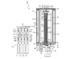
- FIG. 2 is a schematic cross-sectional view illustrating an example of a film forming apparatus for forming a photoconductor layer of the electrophotographic photoconductor illustrated in FIG. 1.
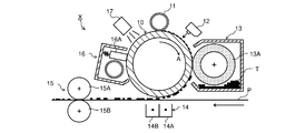
- FIG. 1 is a schematic cross-sectional view illustrating a schematic configuration of an example of an embodiment of an image forming apparatus according to the present disclosure.
- FIG. 1A is a cross-sectional view illustrating a schematic configuration of an example of an embodiment of an electrophotographic photosensitive member according to the present disclosure
- FIG. 1B is a part (corresponding to a portion A) of the first electrophotographic photosensitive member
- FIG. 1C is a cross-sectional view showing an enlarged part (corresponding to part A) of the second electrophotographic photosensitive member.
- an electrophotographic photosensitive member 10 has a cylindrical conductive substrate 10A and a photosensitive layer 10B formed on the outer peripheral surface of the conductive substrate 10A.
- an electrostatic latent image and a toner image based on an image signal are formed on the surface.
- the electrophotographic photoreceptor 10 has flanges F fixed at both ends as necessary, and is rotatably mounted in the image forming apparatus via the flanges F.
- the conductive substrate 10A serves as a support member of the photoreceptor layer 10B in the electrophotographic photoreceptor 10 (hereinafter, also referred to as the photoreceptor 10), and has at least a surface having conductivity. Is configured.
- the shape of the base 10A in the present example is cylindrical, but is not limited to this, and may be, for example, an endless belt shape.
- the base 10A may have a configuration in which the whole is made of a conductive material such as a metal or an alloy containing a metal, or may be made of a metal or a transparent conductive material on the surface of an insulator made of a synthetic resin or glass or ceramics. By forming a conductive film, the surface may have conductivity.
- Examples of the metal include aluminum (Al), stainless steel (SUS), zinc (Zn), copper (Cu), iron (Fe), titanium (Ti), nickel (Ni), chromium (Cr), molybdenum (Mo), Indium (In), niobium (Nb), tellurium (Te), vanadium (V), palladium (Pd), tantalum (Ta), tin (Sn), platinum (Pt), gold (Au) and silver (Ag) No.
- Examples of the synthetic resin include polyester, polyethylene, polycarbonate, cellulose acetate, polypropylene, polyvinyl chloride, polystyrene, and polyamide.
- Examples of the transparent conductive material include ITO (Indium Tin Oxide) and SnO 2 .
- the base 10A is made of an Al-based alloy (for example, an Al-Mn-based alloy, an Al-Mg-based alloy, or an Al-Mg-Si-based alloy).
- the surface of the substrate 10A on which the photoreceptor layer 10B is formed is subjected to a surface treatment by cutting with a lathe or the like.
- a surface treatment include mirror finishing or linear groove processing.
- the photoreceptor layer 10B is located on the outer peripheral surface of the base 10A, and has a thickness of, for example, 15 ⁇ m or more and 90 ⁇ m or less.
- a thickness of the photoreceptor layer 10B is 15 ⁇ m or more, it is possible to appropriately suppress the occurrence of interference fringes in a recorded image without providing a long-wavelength light absorbing layer, for example.
- the thickness of the photoconductor layer 10B is 90 ⁇ m or less, it is possible to appropriately prevent the photoconductor layer 10B from being peeled off from the base 10A due to the stress of the film.
- the photoreceptor layer 10B has a photosensitive layer 101 located on the substrate 10A and a surface layer 102 located on the photosensitive layer 101.
- the material of the photoreceptor layer 10B include inorganic materials such as amorphous silicon (a-Si), amorphous carbon (aC) and amorphous arsenic (a-Se), and various materials. Any of organic materials may be used.
- the photosensitive layer 101 containing an amorphous silicon material will be described as an example.
- the photoconductor layer 10B shown in FIG. 1B is obtained by laminating a surface layer 102 on a photoconductive layer 101 having a charge injection blocking layer 1012 and a photoconductive layer 1011. Further, a photoreceptor layer 10B shown in FIG. 1C has a surface layer 102 having a first surface layer 1021 and a second surface layer 1022 laminated on a photosensitive layer 101 having a charge injection blocking layer 1012 and a photoconductive layer 1011. Things.
- the charge injection blocking layer 1012 (hereinafter, also referred to as a blocking layer 1012) has a role of preventing charges from the base 10A from being injected into the photoconductive layer 1011. Specifically, the blocking layer 1012 prevents injection of holes (positive charges) from the substrate 10A side to the photoconductive layer 1011 side when a negative charging process is applied to the free surface of the photoconductor layer 10B. It has the function to do.
- the blocking layer 1012 is made of a non-single-crystal material mainly composed of amorphous silicon (amorphous silicon: a-Si).
- the non-single-crystal material means a material including a polycrystalline, microcrystalline, or amorphous portion.
- the blocking layer 1012 contains a Group 15 element of the periodic table.
- the Group 15 elements of the periodic table (hereinafter, also referred to as Group 15 elements) contained in the blocking layer 1012 may be substantially uniformly distributed in the blocking layer 1012 or may be unevenly distributed in the layer thickness direction. You may have the part which does.
- the concentration is distributed so that the concentration is lower in the end region on the base 10A side than in the end region on the photoconductive layer 1011 side in the blocking layer 1012.
- the particles are substantially uniformly distributed in the in-plane direction parallel to the surface of the base 10A.
- the atomic concentration of the Group 15 element in the blocking layer 1012 is, for example, not less than 5 ⁇ 10 17 (1 / cm 3 ) and not more than 5 ⁇ 10 19 (1 / cm 3 ).
- the withstand voltage against the positive charge is sufficiently increased (for example, 1.5 when the atomic concentration of the Group 15 element is 0). (More than double).
- the residual potential may be maintained at a sufficiently low state (for example, a residual potential of ⁇ 20 V or less). Tends to be difficult.
- Group 15 elements include nitrogen (N), phosphorus (P), arsenic (As), antimony (Sb), bismuth (Bi), and the like. From the viewpoint of easy control of the doping concentration of nitrogen, nitrogen or phosphorus is preferable. Among them, nitrogen is more preferable in terms of safety and ease of disposal after use.
- the blocking layer 1012 may further contain at least one of oxygen (O) and an element of Group 13 of the periodic table. It is preferable that the blocking layer 1012 contains oxygen because the adhesion to the base 10A is improved.
- a raw material for introducing a Group 15 element into the blocking layer 1012 for example, N 2 , NH 3 , NO, N 2 O, PH 3 , PF 3 , PF 5 , and AsH 3 can be mentioned.
- Raw materials for introducing oxygen include, for example, O 2 , NO, and N 2 O.
- boron hydride such as B 2 H 6 and B 4 H 10
- boron halide such as BF 3 , BCl 3 and BBr 3 , or AlCl 3 and GaCl 3 , Ga (CH 3 ) 3 , InCl 3 or TlCl 3 .
- the blocking layer 1012 may further contain carbon (C).
- C carbon
- the blocking layer 1012 contains carbon
- the effect of improving the adhesion to the substrate 10A can be expected, and the effect of preventing charge injection from the substrate 10A can be expected to be improved.
- a material for introducing carbon into the blocking layer 1012 for example, CH 4 , C 2 H 2 , C 2 H 6 , C 3 H 8 , C 4 H 10 and the like can be mentioned.
- Each of the above-mentioned additional elements may be substantially uniformly distributed in the blocking layer 1012, or may have a portion which is unevenly distributed in the layer thickness direction.
- the additive element is contained so as to increase the concentration of the additional element on the side of the base 10A from the viewpoint of reducing the generation of residual charges.
- the particles are substantially uniformly distributed in the in-plane direction parallel to the surface of the base 10A.
- the thickness of the blocking layer 1012 is set to 0.1 ⁇ m or more and 10 ⁇ m or less from the viewpoint of desired electrophotographic characteristics and economic effects. If the thickness of the blocking layer 1012 is less than 0.1 ⁇ m, it may not be possible to sufficiently prevent charge injection from the substrate 10A side. On the other hand, if the thickness of the blocking layer 1012 exceeds 10 ⁇ m, residual charges may be generated, and the memory characteristics may be deteriorated.
- the photoconductive layer 1011 has a role of generating carriers by light irradiation such as a laser beam.
- the photoconductive layer 1011 is mainly composed of a-Si. That is, it is made of an amorphous (non-single-crystal) material mainly composed of silicon (Si), and when it contains microcrystalline silicon, the dark conductivity / photoconductivity can be increased, and The design flexibility of the layer 1011 can be increased.
- Such microcrystalline silicon can be formed by changing film formation conditions. For example, when the glow discharge decomposition method is employed, the formation can be performed by setting the temperature of the substrate 10A and the DC pulse power to be higher, and increasing the flow rate of the diluent gas (for example, hydrogen).
- the diluent gas for example, hydrogen
- the photoconductive layer 1011 preferably contains at least one of hydrogen and a halogen element from the viewpoint of compensating for dangling bonds of silicon. It is preferable that the total content of hydrogen and halogen elements in the photoconductive layer 1011 be 1 atomic% or more and 40 atomic% or less with respect to the total content of silicon, hydrogen and halogen elements.
- Raw materials for introducing silicon into the photoconductive layer 1011 include silicon hydrides (silanes) such as SiH 4 , Si 2 H 6 , Si 3 H 8, and Si 4 H 10 , among which silicon supply efficiency Alternatively, SiH 4 and Si 2 H 6 are particularly preferable from the viewpoint of easy handling.
- Raw materials for introducing a halogen element into the photoconductive layer 1011 include F 2 , BrF, ClF, ClF 3 , BrF 3 , BrF 5 , IF 3 , IF 7 , SiF 4 and Si 2 F 6 . Note that the raw material for introducing silicon into the photoconductive layer 1011 may be diluted with at least one of H 2 and He as necessary.
- the temperature of the substrate 10A the supply amount of a raw material for introducing each element into the photoconductive layer 1011, or the discharge power of glow discharge decomposition, etc. Adjust it.
- a conductivity control element for controlling conductivity may be introduced into the photoconductive layer 1011.
- the conductivity control element include a Group 13 element that imparts p-type conductivity and a Group 15 element that imparts n-type conductivity. From the viewpoint of sensitivity to semiconductor characteristics or light sensitivity, boron is preferable as the Group 13 element and phosphorus is preferable as the Group 15 element. In particular, it is preferable to use a Group 13 element as the conductivity control element in order to make the photoconductive layer 1011 closer to the intrinsic type (i-type).
- the introduction of the conductivity control element into the photoconductive layer 1011 is performed by, during the formation of the layer, the raw material for introducing the main constituent element of the photoconductive layer 1011 and the above-described raw material for introducing the conductivity control element into a reaction vessel. Perform by supplying. Further, the raw material for introducing the conductivity control element may be diluted with a gas such as H 2 , He, Ar, and Ne as needed. Furthermore, by changing the content of the conductivity control element in the raw material over time or changing the degree of dilution, the concentration of the conductivity control element in the photoconductive layer 1011 can be changed in the layer thickness direction. Good. In the case of such a configuration, the content of the conductivity control element in the photoconductive layer 1011 may be such that the average content in the entire photoconductive layer 1011 is within a predetermined range.
- the photoconductive layer 1011 may contain at least one element of carbon, oxygen, and nitrogen.
- the total content of carbon, oxygen and nitrogen in the photoconductive layer 1011 is preferably 1 ⁇ 10 ⁇ 5 atomic% or more and 10 atomic% or less with respect to the total amount of these elements and silicon.
- the thickness (layer thickness) of the photoconductive layer 1011 is set to 5 ⁇ m or more and 100 ⁇ m or less (preferably 10 ⁇ m or more and 80 ⁇ m or less) from the viewpoint of desired electrophotographic characteristics and economic effects. If the thickness of the photoconductive layer 1011 is less than 5 ⁇ m, charging ability or photosensitivity may not be sufficiently secured. On the other hand, if the thickness of the photoconductive layer 1011 exceeds 100 ⁇ m, the thickness becomes unnecessary in terms of electrophotographic characteristics, the formation time is lengthened, and the production cost is increased.
- the photosensitive layer 10B may have an upper charge injection blocking layer (also referred to as an upper blocking layer) located on the photoconductive layer 1011.
- the upper blocking layer plays a role of preventing charges charged on the surface of the photoconductor layer 10B by the charger in the image forming apparatus from being injected into the photoconductive layer 1011 side.
- a-Si is mainly used and a group 13 element is included.
- Group 13 elements include boron (B), aluminum (Al), gallium (Ga), indium (In), and thallium (Tl).
- the upper blocking layer may further include at least one of nitrogen, oxygen and carbon.
- the surface layer 102 (the first surface layer 1021 and the second surface layer 1022) mainly has a role of improving the moisture resistance, the repeated use characteristic, the electric pressure resistance, the use environment characteristic or the durability of the photoreceptor 10.
- the surface layer 102 is made of a-SiC, a-SiN which is an amorphous material mainly containing, for example, silicon and at least one of carbon, nitrogen, and oxygen.
- A-SiO, a-SiCNO, etc. made of aC which is an amorphous material mainly composed of carbon, or an inorganic material such as DLC (diamond-like carbon).
- the surface layer 102 is composed of an organic material such as polyester, polycarbonate, polystyrene, or polyvinyl acetate, or a liquid material such as an isoparaffin-based solvent, silicone oil, or a higher fatty acid ester.
- an organic material such as polyester, polycarbonate, polystyrene, or polyvinyl acetate
- a liquid material such as an isoparaffin-based solvent, silicone oil, or a higher fatty acid ester.
- the content of carbon in a-SiC should be 40 atom% or more and 90 atom% or less with respect to the sum of silicon and carbon. Some are preferred.
- a-SiC preferably contains at least one of hydrogen and a halogen element from the viewpoint of compensating for dangling bonds of silicon. Their content is preferably at least 1 at.% And at most 70 at.% (Preferably at least 1 at.% And at most 45 at.%) With respect to the total of the constituent elements.
- the refractive index n1 of the surface layer 102 is in the range of 1 ⁇ n1 ⁇ n0 when the refractive index of the photosensitive layer 101 is n0. .
- n1 is preferably in the range of ⁇ n0 ⁇ 0.2, that is, n01 / 2 ⁇ 0.2.
- n1 is preferably in the range of 1.8 to 2.2.
- the value of the refractive index n0 of the photosensitive layer 101 is determined depending on the material.
- the average height Rc0 of the photosensitive layer 101 on the light incident side may be ⁇ / (4 ⁇ n1) or more with respect to the wavelength ⁇ of the exposure and the refractive index n1 of the surface layer 102. That is, ⁇ / (4 ⁇ n1) ⁇ Rc0.
- Rc0 may be 81.25 nm or more.
- Rc1 is made smaller than Rc0. That is, Rc1 ⁇ / (4 ⁇ n1).
- Rc1 has a small value, and it is preferable that the surface of the surface layer 102 is smooth.
- Rc1 is preferably 30 nm or less.
- the thickness (layer thickness) of the surface layer 102 is set to 0.2 ⁇ m or more and 1.5 ⁇ m or less (preferably 0.5 ⁇ m or more and 1 ⁇ m or less) from the viewpoint of durability or residual potential.
- the relationship between the refractive index and the average height of the surface layer 102 and the photosensitive layer 101 in the first photosensitive member 10 is determined by the first relationship.
- the refractive index n1 of the first surface layer 1021 is in the range of 1 ⁇ n1 ⁇ n2, where n2 is the refractive index of the second surface layer 1022.
- n1 is preferably in the range of ⁇ n2 ⁇ 0.2, that is, n21 / 2 ⁇ 0.2.
- n1 is preferably in the range of 1.21 to 1.61.
- the average height Rc2 of the exposure surface of the second surface layer 1022 on the incident side may be ⁇ / (4 ⁇ n1) or more with respect to the wavelength ⁇ of the exposure and the refractive index n1 of the first surface layer 1021. That is, ⁇ / (4 ⁇ n1) ⁇ Rc2.
- Rc2 may be 116 nm or more.
- Rc1 is made smaller than Rc2. That is, Rc1 ⁇ / (4 ⁇ n1).
- Rc1 has a small value, and it is preferable that the surface of the first surface layer 1021 is smooth.
- Rc1 is preferably 30 nm or less.
- the total thickness (layer thickness) of the first surface layer 1021 and the second surface layer 1022 is 0.2 ⁇ m or more and 1.5 ⁇ m or less (preferably 0.5 ⁇ m or more and 1 ⁇ m or less) from the viewpoint of durability or residual potential. Is set. Regarding the ratio of the thickness of the first surface layer 1021 to the thickness of the second surface layer 1022, the thickness of the second surface layer 1022 is made smaller than the thickness of the first surface layer 1021 in consideration of the relationship between the average heights Rc1 and Rc2 of the surfaces. Is also preferable, but there is no particular limitation.
- the present disclosure relates to the interface between the photosensitive layer 101 and the surface layer 102 or the interface between the second surface layer 1022 and the first surface layer 1021, and the surface of the surface layer 102 (the surface of the first surface layer 1021). This suppresses multiple reflections between the images, suppresses the occurrence of interference fringes, and suppresses the occurrence of interference fringe-like density unevenness in an image.
- the present disclosure sets the refractive index and the average height as described above to suppress the occurrence of interference fringes due to exposure on the surface layer 102.
- the thickness of the surface layer 102 is set to 0.2 ⁇ m or more and 1.5 ⁇ m or less (preferably 0.5 ⁇ m or more and 1 ⁇ m or less) from the viewpoint of durability or residual potential. If the thickness of the surface layer 102 is less than 0.2 ⁇ m, the occurrence of image flaws or uneven image density may not be sufficiently suppressed in printing durability in an image forming apparatus. On the other hand, if the thickness of the surface layer 102 exceeds 1.5 ⁇ m, the occurrence of image defects due to the residual potential may not be properly suppressed.
- the photosensitive layer 101 may be made of an inorganic material such as an amorphous arsenic-based material or various organic materials used for laser printers, in addition to the material containing an amorphous silicon material.
- an amorphous silicon material when the photosensitive layer 101 contains an amorphous silicon material and the exposure wavelength ⁇ is 680 nm or less, it suppresses the occurrence of interference fringes due to exposure, suppresses the occurrence of density unevenness in an image, and improves durability. This is preferable in that an excellent photoconductor 10 can be obtained.
- the wavelength ⁇ is 400 nm or more, which is the lower limit of the sensitivity of the photosensitive layer 101.
- the photosensitive layer 101 contains an organic material using a phthalocyanine-based material and the exposure wavelength ⁇ is 770 to 790 nm, the photosensitivity is good, and the occurrence of interference fringes due to the exposure is suppressed, and the image density unevenness is reduced. This is preferable in that the photosensitive member 10 having practical durability can be obtained.
- the surface layer 102 may be formed of the above-described amorphous material, the above-described resin that is the organic material, or the above-described liquid that is the liquid material. preferable.
- the surface layer 102 is made of an amorphous material, the unevenness of the average height Rc0 on the light incident side of the photosensitive layer 101 tends to be reflected on the surface, but the average height Rc1 of the surface is polished.
- the surface layer 102 having excellent durability can be obtained by reducing the size and smoothing.
- the surface layer 102 is made of a resin or a liquid, the average height Rc1 on the light incident side of the exposure becomes small and the surface becomes easy to be smooth. The effect of the disclosed photoreceptor 10 can be obtained favorably.
- the first surface layer 1021 is also preferably made of the above-mentioned amorphous material, the above-mentioned organic resin, or the above-mentioned liquid material.
- the first surface layer 1021 is made of an amorphous material, the unevenness of the average height Rc2 on the incident side of exposure of the second surface layer 1022 tends to be easily reflected on the surface.
- the height Rc1 By polishing or the like and smoothing it, the first surface layer 1021 having excellent durability can be obtained.
- the first surface layer 1021 is made of a resin or a liquid, the average height Rc1 on the light incident side of the exposure becomes small and the surface becomes easy to be smooth.
- the influence of the unevenness of the average height Rc2 of the second surface layer 1022 is reduced. And the effects of the photoconductor 10 of the present disclosure can be obtained favorably.
- the first surface layer 1021 is made of a liquid
- a part of the developing solution is supplied as a material constituting the first surface layer 1021 by employing liquid development, so that the liquid can be stably maintained even in the liquid state.
- the first surface layer 1021 can be maintained.
- FIG. 2 shows an example of a plasma CVD apparatus Y which is a film forming apparatus for forming a photosensitive layer 101 (a blocking layer 1012, a photoconductive layer 1011) and a surface layer 102 on a substrate 10A by a glow discharge decomposition method. It is a schematic block diagram.
- the plasma CVD apparatus Y includes a reaction chamber 20, a support mechanism 30, a DC voltage supply mechanism 40, a temperature control mechanism 50, a rotation mechanism 60, a gas supply mechanism 70, and an exhaust mechanism 80.
- the reaction chamber 20 is a space for forming a deposited film to be each layer on the substrate 10A, and is partitioned by a cylindrical electrode 21, a pair of plates 22, 23, and insulating members 24, 25.
- the cylindrical electrode 21 serves as a second conductor when the base 10A is used as a first conductor in order to generate a glow discharge and partition a space in which a deposited film is formed.
- the cylindrical electrode 21 is made of the same conductive material as the base 10A, and is integrated with a pair of plates 22 and 23 via insulating members 24 and 25.
- the cylindrical electrode 21 in this example is configured so that the distance between the base 10A supported by the support mechanism 30 and the cylindrical electrode 21 is 10 mm or more and 100 mm or less. If the distance between the base 10A and the cylindrical electrode 21 is smaller than 10 mm, it may be difficult to obtain a stable discharge between the base 10A and the cylindrical electrode 21.
- the power for obtaining a stable discharge becomes unnecessarily large, and the plasma CVD apparatus Y becomes unnecessarily large.
- the productivity per hit may decrease.
- the cylindrical electrode 21 has a gas inlet 21a and a plurality of gas outlets 21b, and one end thereof is grounded.
- the grounding of the cylindrical electrode 21 is not an essential condition, and may be configured to be connected to a reference power supply different from a DC power supply 41 described later.
- the reference voltage of the reference power supply is, for example, -1500V or more and 1500V or less.
- the gas inlet 21 a is an opening for introducing a cleaning gas or a source gas into the reaction chamber 20, and is connected to the gas supply mechanism 70.
- the plurality of gas blowing holes 21b are openings for blowing the cleaning gas or the raw material gas introduced into the inside of the cylindrical electrode 21 toward the base 10A, and are arranged, for example, at equal intervals in the vertical direction and the circumferential direction in the drawing. You.
- the plurality of gas blowing holes 21b are formed in the same circular shape, and the hole diameter is, for example, 0.5 mm or more and 2 mm or less. The diameter, shape and arrangement of the plurality of gas blowing holes 21b can be changed as appropriate.
- the plate 22 is configured to be detachable so that the open state and the closed state of the reaction chamber 20 can be selected, and by opening and closing the plate 22, a support 31 described below can be taken in and out of the reaction chamber 20. It is possible.
- the plate 22 is formed of the same conductive material as that of the base 10A, and has an adhesion preventing plate 26 attached to the lower surface thereof. As a result, formation of a deposited film on the plate 22 is prevented.
- the attachment-preventing plate 26 is formed of the same conductive material as the base 10A, and is detachable from the plate 22.
- the plate 23 serves as a base of the reaction chamber 20, and is made of the same conductive material as the base 10A.
- the insulating member 25 interposed between the plate 23 and the cylindrical electrode 21 has a role of suppressing the occurrence of arc discharge between the cylindrical electrode 21 and the plate 23.
- Such an insulating member 25 can be formed of, for example, various glass materials, inorganic insulating materials such as ceramics, or various synthetic resin insulating materials such as fluororesin or polycarbonate.
- the material of the insulating member 25 is not particularly limited as long as it has insulating properties, has sufficient heat resistance at a use temperature, and emits a small amount of gas in a vacuum.
- the plate 23 and the insulating member 25 are provided with gas outlets 23A and 25A and a pressure gauge 27.
- the gas discharge ports 23A and 25A serve to discharge the gas inside the reaction chamber 20, and are connected to the exhaust mechanism 80.
- the pressure gauge 27 is for monitoring the pressure in the reaction chamber 20, and various known ones can be used.
- the support mechanism 30 supports the base 10A and plays a role as a first conductor for generating a glow discharge.
- the support mechanism 30 is configured to include a support 31, a conductive support 32, and an insulating material 33.
- the support mechanism 30 in this example is formed to have a length (dimension) that can support the two bases 10A, and the support 31 is detachable from the conductive support 32. According to such a configuration, the two substrates 10A can be moved in and out of the reaction chamber 20 without directly touching the surfaces of the two substrates 10A supported.
- the support 31 is a hollow member having a flange portion 31a, and is entirely formed of a conductor using the same conductive material as the base 10A.
- the conductive support 32 is a cylindrical member having a conductive plate 32a, and is formed entirely of a conductive material using the same conductive material as the base 10A.
- the conductive support 32 is configured to contact the inner wall surface of the support 31 at the upper end.
- the insulating material 33 plays a role of ensuring electrical insulation between the conductive support 32 and the plate 23, and is interposed between the conductive support 32 and the plate 23 at substantially the center of the reaction chamber 20. ing.
- the DC voltage supply mechanism 40 is a mechanism for supplying a DC voltage to the conductive support 32, and has a DC power supply 41 and a control unit 42.
- the DC power supply 41 plays a role of generating a DC voltage to be applied to the conductive support 32, and is connected to the conductive support 32 via the conductive plate 32a.
- the control unit 42 controls the operation of the DC power supply 41, and is connected to the DC power supply 41.
- the control unit 42 is configured to control the operation of the DC power supply 41 so as to apply, for example, a pulsed DC voltage to the support 31 via the conductive support 32.
- the temperature control mechanism 50 controls the temperature of the base 10A, and has a ceramic pipe 51 and a heater 52.
- the ceramic pipe 51 plays a role of ensuring insulation and thermal conductivity, and is housed inside the conductive support 32.
- the heater 52 plays a role of heating the base 10A, and is housed inside the conductive support 32.
- the temperature of the base 10A is controlled, for example, by attaching a thermocouple (not shown) to the support 31 or the conductive support 32 and controlling the heater 52 on / off based on the monitoring result.
- the temperature of the base 10A is maintained at a predetermined temperature in a range of, for example, 200 ° C. or more and 400 ° C. or less.
- the heater 52 is, for example, a nichrome wire or a cartridge heater.
- the rotation mechanism 60 serves to rotate the support 31 and includes a rotation motor 61, a rotation introduction terminal 62, an insulating shaft member 63, and an insulating flat plate 64.
- the support mechanism 30 is rotated by the rotation mechanism 60 to form a film
- the base 10A rotates together with the support 31, so that the decomposition components of the source gas are preferably deposited substantially uniformly on the outer periphery of the base 10A. It is.
- the rotary motor 61 has a role of applying a rotational force to the base 10A.
- the operation of the rotary motor 61 is controlled so as to rotate the base 10A at a constant rotation speed of 1 rpm or more and 10 rpm or less, for example.
- the rotation introducing terminal 62 has a role of transmitting a rotational force to the insulating shaft member 63 while maintaining the inside of the reaction chamber 20 at a predetermined degree of vacuum.
- a vacuum sealing means such as an oil seal or a mechanical seal having a double or triple rotation shaft can be used.
- the insulating shaft member 63 and the insulating plate 64 serve to transmit the rotational force from the rotary motor 61 via the rotation introducing terminal 62 to the support mechanism 30 while maintaining the insulating state between the support mechanism 30 and the plate 22. It is responsible. These are formed of the same insulating material as the insulating member 25, for example.
- the insulating flat plate 64 plays a role in preventing foreign substances such as dust or dust falling when the plate 22 is removed from attaching to the base 10A.
- an insulating flat plate 64 is provided, it is possible to suppress the occurrence of abnormal discharge due to the attachment of foreign matter to the base 10A, and to suppress the occurrence of film formation defects.
- the gas supply mechanism 70 includes a plurality of source gas tanks 71 to 74, a plurality of pipes 71A to 74A, a plurality of valves 71B to 74B, 71C to 74C, and a plurality of mass flow controllers 71D to 74D. And a cylindrical electrode 21 via a gas inlet 21a.
- Each of the source gas tanks 71 to 74 is filled with a source gas.
- a source gas for example, SiH 4 , H 2 , B 2 H 6 , CH 4 , N 2 or NO is used.
- the valves 71B to 74B, 71C to 74C and the mass flow controllers 71D to 74D are for adjusting the flow rate, composition and gas pressure of the gas components introduced into the reaction chamber 20.
- the type of gas to be filled in each of the source gas tanks 71 to 74 or the number of the plurality of source gas tanks 71 to 74 is appropriately selected according to the type or composition of the film to be formed on the base 10A. do it.
- the exhaust mechanism 80 has a role of discharging the gas in the reaction chamber 20 to the outside through the gas discharge ports 23A and 25A, and has, for example, a mechanical booster pump 81 and a rotary pump 82.
- the operation of these pumps 81 and 82 is controlled based on the result of monitoring by the pressure gauge 27. That is, in the exhaust mechanism 80, based on the monitoring result of the pressure gauge 27, the reaction chamber 20 is maintained in a predetermined vacuum state, and the gas pressure in the reaction chamber 20 is set to a target value.
- the pressure in the reaction chamber 20 is, for example, 1 Pa or more and 100 Pa or less.
- a support mechanism 30 supporting a plurality of (two in FIG. 2) substrates 10A is set inside the reaction chamber 20, and the plate 22 is attached again.
- the two bases 10A are supported by the support mechanism 30 by sequentially stacking the lower dummy base D1, the base 10A, the intermediate dummy base D2, the base 10A, and the upper dummy base D3 on the flange 31a of the support 31.
- the dummy bases D1 to D3 for example, one having a configuration having conductivity as a whole or a configuration having a conductive film formed on the surface of an insulator can be used. Is particularly preferred.
- the lower dummy base D1 mainly has a role of adjusting the height position of the base 10A.
- the intermediate dummy substrate D2 mainly has a role of suppressing generation of uneven discharge between the ends of the adjacent substrates 10A.
- the length of the intermediate dummy substrate D2 is set to a length (for example, 1 cm or more) that can sufficiently suppress generation of uneven discharge.
- a curved surface for example, a radius of curvature of 0.5 mm or more
- a chamfering process (the length of the cut portion in the axial direction and the length in the depth direction is 0.5 mm or more, respectively) is applied to the outer peripheral surface side corner. Is adopted.
- the upper dummy base D3 mainly has a role of suppressing formation of a deposited film on the support 31. As the upper dummy base D3, a base whose upper end protrudes above the uppermost part of the support 31 is employed.
- the temperature of the base 10A is controlled to a predetermined temperature by the temperature control mechanism 50, and the pressure in the reaction chamber 20 is reduced by the exhaust mechanism 80.
- the temperature control of the base body 10A is performed such that the heater 52 is heated to near a predetermined temperature by generating heat, and then the heater 52 is turned on / off to maintain the predetermined temperature.
- the temperature of the substrate 10A is appropriately set depending on the type and composition of the film to be formed on the surface thereof. For example, when forming an a-Si film, the temperature is set in the range of 250 ° C. to 300 ° C.
- the pressure in the reaction chamber 20 is reduced by controlling the operation of the mechanical booster pump 81 and the rotary pump 82 while monitoring the pressure of the reaction chamber 20 with the pressure gauge 27, so that the reaction is performed through the gas outlets 23A and 25A. This is performed by discharging gas from the chamber 20.
- the pressure in the reaction chamber 20 before the introduction of the source gas is reduced, for example, to about 1 ⁇ 10 ⁇ 3 Pa.
- a raw material gas is supplied to the reaction chamber 20 by the gas supply mechanism 70, and the cylindrical electrode 21 and the support 31 are During this time, for example, a pulsed DC voltage is applied. As a result, a glow discharge is generated between the cylindrical electrode 21 and the support 31 (base 10A) to decompose the raw material gas, and the decomposed components are deposited on the surface of the base 10A.
- the pressure in the reaction chamber 20 is maintained in a predetermined range (for example, 1 Pa or more and 100 Pa or less) by controlling the operations of the mechanical booster pump 81 and the rotary pump 82 while monitoring with the pressure gauge 27. That is, the pressure inside the reaction chamber 20 is maintained in a predetermined range by the mass flow controllers 71D to 74D in the gas supply mechanism 70 and the pumps 81 and 82 in the exhaust mechanism 80.
- the raw material gas is supplied to the reaction chamber 20 by controlling the mass flow controllers 71D to 74D while appropriately controlling the open / close states of the valves 71B to 74B and 71C to 74C. This is performed by introducing the composition and flow rate into the cylindrical electrode 21 through the pipes 71A to 74A and 75 and the gas inlet 21a. The raw material gas introduced into the cylindrical electrode 21 is blown out toward the base 10A through the plurality of gas blowout holes 21b. Then, the composition of the source gas is appropriately changed by the valves 71B to 74B, 71C to 74C and the mass flow controllers 71D to 74D.
- the application of the pulsed DC voltage between the cylindrical electrode 21 and the support 31 is performed when the cylindrical electrode 21 is grounded, in a range from ⁇ 3000 V to ⁇ 50 V (preferably from ⁇ 3000 V to ⁇ 500 V). ) Is performed so as to be a negative pulsed DC potential V1.
- the potential difference ⁇ V (for example, ⁇ 3000 V or more and ⁇ 50 V or less) is set as the potential V2 supplied from the reference power supply. It is done to become.
- a negative pulse voltage is applied to the support 31 (base 10A)
- the potential V2 supplied from the reference power supply is set to, for example, -1500 V or more and 1500 V or less.
- the control unit 42 controls the DC power supply 41 so that the frequency (1 / T (second)) of the DC voltage is 300 kHz or less and the duty ratio (T1 / T) is 20% or more and 90% or less.
- the photosensitive layer 101 (the blocking layer 1012 and the photoconductive layer 1011) and the surface layer 102 are sequentially laminated on the surface of the substrate 10A.
- the image forming apparatus of the present disclosure since the image forming apparatus of the present disclosure includes the electrophotographic photoreceptor of the present disclosure, the same effects as those of the electrophotographic photoreceptor of the present disclosure can be obtained. That is, it is possible to maintain good image quality by hardly causing an image defect that appears as a black dot on an image when printing with an image forming apparatus.
- FIG. 3 is a schematic cross-sectional view illustrating a schematic configuration of an example of an embodiment of an image forming apparatus according to the present disclosure.
- the image forming apparatus X of this embodiment employs the Carlson method of electrophotography as an image forming method.
- a photoconductor 10 a charger 11, an exposure unit 12, a developing unit 13, a transfer unit 14, a fixing device 15, a cleaning device 16, and a static eliminator 17 are provided.
- the charger 11 serves to charge the surface of the photoconductor 10 to a negative polarity here.
- the charging voltage is set to, for example, ⁇ 1000 V or more and ⁇ 200 V or less.
- a contact-type charger configured by coating a core metal with conductive rubber and polyvinylidene fluoride is used, but instead, a non-contact type charger including a discharge wire is used.
- a device for example, a corona charger may be employed.
- the exposure device 12 has a role of forming an electrostatic latent image on the charged photoconductor 10.
- the exposure device 12 has a wavelength ⁇ (for example, 650 nm if the photosensitive layer 101 is made of a material containing an amorphous silicon material) that is sufficiently absorbed by the photosensitive layer 101 according to an image signal.
- exposure light eg, laser light
- the wavelength ⁇ of this exposure depends on the photosensitivity of the photoconductor 10, but is preferably, for example, 400 to 680 nm.
- the developing device 13 has a role of developing the electrostatic latent image on the photoconductor 10 to form a toner image.
- the developing device 13 in this embodiment is of a dry developing type and includes a magnetic roller 13A for magnetically holding a developer (toner) T.
- the developer T forms a toner image formed on the surface of the photoreceptor 10 and is frictionally charged in the developing device 13.
- Examples of the developer T include a two-component developer containing a magnetic carrier and an insulating toner, and a one-component developer containing a magnetic toner.
- the magnetic roller 13A plays a role of transporting the developer to the surface (development area) of the photoconductor 10.
- the magnetic roller 13A conveys the developer T frictionally charged in the developing device 13 in the form of a magnetic brush adjusted to a constant spike length.
- the transported developer T adheres to the surface of the photoconductor 10 by the electrostatic attraction of the electrostatic latent image in the development area of the photoconductor 10 to form a toner image (visualizes the electrostatic latent image).
- the charge polarity of the toner image is opposite to the charge polarity of the surface of the photoconductor 10 when performing image formation by regular development, and is the polarity of charge on the surface of the photoconductor 10 when performing image formation by reverse development. And have the same polarity.
- the developing device 13 may be a liquid developing type developing device.
- the liquid developing type developing device includes a liquid developer tank for storing a liquid developer containing toner outside the developing device.
- the liquid developer includes toner particles and a carrier liquid that is an insulating liquid.
- the carrier liquid is a non-polar, ie, electrically neutral, solvent such as silicone oil, and is adjusted so that the toner particles are dispersed therein at a high concentration.
- the toner particles are composed of a binder resin such as epoxy, a charge control agent that gives a predetermined charge to the toner, a coloring pigment, and the like.
- the developing roller supplied with the liquid developer contacts the surface of the photoconductor 10 and the liquid Supply developer. Then, by supplying the liquid developer from the developing roller as a developer carrier to the photoconductor 10 on which the electrostatic latent image is formed, a toner image can be formed on the photoconductor 10.
- the carrier liquid is also applied in a layer form on the surface of the photoreceptor 10, and this liquid can optically function as a part of the surface layer 102 or the first surface layer 1021.
- the transfer device 14 has a function of transferring the toner image of the photoconductor 10 to the recording medium P supplied to the transfer area between the photoconductor 10 and the transfer device 14.
- the transfer device 14 in this example includes a transfer discharger 14A and a separation discharger 14B.
- the transfer unit 14 the back surface (non-recording surface) of the recording medium P is charged to a polarity opposite to that of the toner image by the transfer discharging unit 14A, and the toner is placed on the recording medium P by electrostatic attraction between the charged charge and the toner image. The image is transferred. Further, in the transfer unit 14, at the same time as the transfer of the toner image, the back surface of the recording medium P is erased by the AC discharge in the separation discharge unit 14B, and the recording medium P is quickly separated from the surface of the photoconductor 10. .
- the transfer device 14 may be a transfer roller that is driven by the rotation of the photoconductor 10 and that is arranged with a small gap (usually 0.5 mm or less) from the photoconductor 10.
- the transfer roller is configured to apply a transfer voltage that attracts the toner image on the photoconductor 10 onto the recording medium P using, for example, a DC power supply.
- a transfer separation device such as the separation discharger 14B can be omitted.
- the fixing device 15 serves to fix the toner image transferred on the recording medium P to the recording medium P, and includes a pair of fixing rollers 15A and 15B.
- the fixing rollers 15A and 15B for example, a metal roller whose surface is coated with polytetrafluoroethylene or the like is used.
- a toner image can be fixed on the recording medium P by applying heat and pressure to the recording medium P passing between the pair of fixing rollers 15A and 15B.
- the cleaning device 16 serves to remove toner remaining on the surface of the photoconductor 10 after transfer.
- the cleaning device 16 of this embodiment includes a cleaning blade 16A.
- the cleaning blade 16A plays a role of scraping residual toner from the surface of the photoconductor 10.
- the cleaning blade 16A is formed of, for example, a rubber material containing a polyurethane resin as a main component.
- the static eliminator 17 plays a role in removing the surface charge of the photoconductor 10 remaining as an electrostatic latent image.
- the static eliminator 17 of the present example performs static elimination by exposing the photoconductor 10, and is capable of emitting light of a specific wavelength (for example, 780 nm or more).
- the static eliminator 17 is configured to remove the surface charge (residual electrostatic latent image) of the photoconductor 10 by irradiating the entire surface of the photoconductor 10 in the axial direction using a light source such as an LED. ing.
- a photoreceptor layer was formed on the surface of the cylindrical substrate under the following conditions using the film forming apparatus shown in FIG. 2 to produce a photoreceptor.
- An aluminum alloy base tube (outer diameter 30 mm, length 360 mm) was used as the base.
- the base tube was subjected to chamfering at the end and mirror-finishing the outer peripheral surface to obtain a base.
- the substrate is carried into a clean room, subjected to precision cleaning for removing oil and the like, set in the reaction chamber of the film forming apparatus shown in FIG. 2, and exposed to the outer peripheral surface of the substrate using the above-described film forming method.
- a body layer was formed.
- the configuration of each layer in the photoconductor layer is as follows.
- the blocking layer is made of an a-Si material obtained by adding nitrogen (N) and oxygen (O) to a-Si, and containing boron (B) as a dopant, and has a thickness of 6 ⁇ m.
- the photoconductive layer was made of a-Si containing boron (B) as a dopant, and had a thickness of 14 ⁇ m.
- the refractive index n0 of this photoconductive layer was 4.4.
- the surface layer had a configuration in which an a-SiC-based layer was continuously changed from an a-C-based layer, and the total thickness was 1 ⁇ m.
- the refractive index n1 of this surface layer was 1.9.
- the outer surface (surface) of the photoconductive layer was subjected to a cutting process on the surface of the photosensitive layer under the conditions shown in Table 1 so as to have a regularly repeated uneven shape.
- the surface of the photosensitive layer was made to have irregular irregularities under the conditions shown in Table 2 by blasting the outer peripheral surface.
- the average height Rc0 of the surface of these photosensitive layers (the surface on the incident side of exposure) is ⁇ / (4) while the wavelength ⁇ of exposure for forming an electrostatic latent image is 650 nm (0.65 ⁇ m).
- ⁇ n1) was 0.0855 ⁇ m (85.5 nm), so all of the values were higher than that.
- the base pipe having a regularly repeated irregular shape on the surface under the conditions shown in Table 3 by cutting the outer peripheral surface of the raw tube having the chamfered end portion and the mirror-finished outer peripheral surface. And Similarly, a substrate having irregular irregularities on the surface under the conditions shown in Table 4 was obtained by blasting the outer peripheral surface.
- the blocking layer was made of an a-Si-based material obtained by adding N and O to a-Si and containing B as a dopant, and had a thickness of 6 ⁇ m.
- the photoconductive layer was made of a-Si containing B as a dopant, and had a thickness of 14 ⁇ m.
- the surface layer was composed of the second surface layer and the first surface layer.
- the second surface layer was a layer made of an a-SiC-based amorphous material and had a thickness of 1 ⁇ m.
- the refractive index n2 was 1.9.
- the first surface layer was a layer made of an isoparaffin-based solvent, and had a thickness of 2 ⁇ m. Further, the refractive index n1 was 1.4.
- the average height Rc2 of the surface of the second surface layer (the surface on the incident side of exposure) reflects the average height Rc of the surface of the substrate, and is the same as Rc shown in Tables 3 and 4. Value. Since the average height Rc2 is 650 nm (0.65 ⁇ m) for exposure for forming an electrostatic latent image and ⁇ / (4 ⁇ n1) is 0.116 ⁇ m (116 nm), All were higher values.
- the average height Rc1 of the surface of the first surface layer (the surface on the incident side of exposure) is smaller than the average height Rc2 of the surface of the second surface layer, and is less than ⁇ / (4 ⁇ n1). Value.
- the base tube was subjected to chamfering of the end portion and mirror finishing of the outer peripheral surface to obtain a base.
- the substrate is carried into a clean room, subjected to precision cleaning for removing oil and the like, set in the reaction chamber of the film forming apparatus shown in FIG. 2, and the photosensitive layer is formed on the outer peripheral surface of the substrate using the above-described film forming method. Was formed.
- the configuration of each layer in the photoconductor layer is as follows.
- the blocking layer was made of an a-Si-based material obtained by adding N and O to a-Si and containing B as a dopant, and had a thickness of 6 ⁇ m.
- the photoconductive layer was made of a-Si containing B as a dopant, and had a thickness of 14 ⁇ m.
- the refractive index n0 of this photoconductive layer was 4.4.
- the surface layer had a configuration in which an a-SiC-based layer was continuously changed from an a-C-based layer, and the total thickness was 1 ⁇ m.
- the refractive index n1 of this surface layer was 1.8.
- the average height Rc0 of the surface of the photosensitive layer (the surface on the light incident side) is less than ⁇ / (4 ⁇ n1), and the average height Rc1 of the outermost surface of the surface layer (the surface on the light incident side) is: ⁇ / (4 ⁇ n1), but the average height Rc1 is larger than the surface of the photosensitive layer having the average height Rc0 on the light incident side (the interface between the photosensitive layer and the surface layer).
- a sample as a comparative example of the present disclosure was manufactured.
- the presence or absence of interference fringe-like density unevenness in the image was evaluated by the following method.
- the photoreceptors obtained under the respective conditions were respectively incorporated in a device modified from a laser printer, a color multifunction machine TASKalfa 3550ci manufactured by Kyocera Document Solutions Co., Ltd., and printing was performed. From the printing results, the presence or absence of uneven density in the image was observed and evaluated. As a result, in the samples of Examples Nos. 1 to 12, density unevenness which was a practical problem was not confirmed, whereas in the sample of the comparative example, interference fringe-shaped density unevenness was confirmed.
- the first electrophotographic photoreceptor of the present disclosure has a photosensitive layer located on a conductive substrate, and a surface layer located on the photosensitive layer.
- the average height of the surface layer is Rc1
- the refractive index of the photosensitive layer is n0
- the average height of the photosensitive layer on the incident side of exposure is Rc0, 1 ⁇ n1 ⁇ n0 and Rc1 ⁇ / ( Since 4 ⁇ n1) ⁇ Rc0, it is possible to suppress the occurrence of interference fringes due to exposure between the surface of the photosensitive layer (the interface between the photosensitive layer and the surface layer) and the surface of the surface layer. Good image quality can be maintained by suppressing the occurrence of interference fringe-like density unevenness in an image.
- the second electrophotographic photoreceptor of the present disclosure has a photosensitive layer located on a conductive substrate, and a surface layer located on the photosensitive layer, and the surface layer has a second layer located on the photosensitive layer side.
- the occurrence of interference fringes due to exposure between the surface of the second surface layer (the interface between the second surface layer and the first surface layer) and the surface of the first surface layer can be suppressed.
- the image forming apparatus since the image forming apparatus includes the above-described electrophotographic photosensitive member of the present disclosure, an image having a wavelength ⁇ is scanned on the electrophotographic photosensitive member to form an image to form an electrostatic latent image. Occasionally, it is possible to suppress the occurrence of interference fringe-like density unevenness and maintain good image quality.
- Electrophotographic photoconductor (photoconductor) 10A Conductive substrate (substrate) 10B: Photoconductor layer 101 ... Photosensitive layer 1011... Photoconductive layer 1012... Blocking layer 102... Surface layer 1021 ... First surface layer 1022 second surface layer X image forming apparatus
Landscapes
- Physics & Mathematics (AREA)
- General Physics & Mathematics (AREA)
- Chemical & Material Sciences (AREA)
- Inorganic Chemistry (AREA)
- Photoreceptors In Electrophotography (AREA)
Abstract
本開示の電子写真感光体は、導電性基体と、導電性基体上に位置する感光層と、感光層上に位置する表面層とを有し、表面層の屈折率をn1、露光の入射側の平均高さをRc1とし、感光層の屈折率をn0、露光の入射側の平均高さをRc0としたとき、1<n1<n0であり、かつRc1<λ/(4×n1)≦Rc0である。
Description
本開示は、レーザ光による露光に対して画像に干渉縞状の濃度むらが発生するのを抑制できる感光体層を有する電子写真感光体およびこれを備える画像形成装置に関するものである。
電子写真方式を採用した画像形成装置は、例えばアルミニウム製の円筒状の導電性基体の外周面に感光体層を形成してなる電子写真感光体を備えている。また、画像形成のための電子写真感光体への露光にレーザ光を用いる画像形成装置では、感光体層と導電性基体との界面あるいは感光体層を構成する感光層および表面層といった複数の層の界面と、感光体層の表面(表面層の表面)との間におけるレーザ光の多重反射に起因する干渉縞の発生によって、画像にその干渉縞状の濃度むらが発生することがある。
これに対して、干渉縞状の画像濃度むらの発生を抑制する工夫が種々行なわれている。例えば、導電性基体上に感光層を設けてなる感光体の表面に、波長λ(μm)、スポット径φ(μm)の書き込み光を走査することにより静電画像を形成することからなる画像形成方法において、感光体表面の主走査方向に沿う断面曲線からこの書き込み光のスポット径と実質的に同じ基準長さφを抜き取った部分の最大高さがλ/(2n)以上である(nは書き込み光の波長λ(μm)における感光層の屈折率を表す)ものなどが提案されている(例えば、特開2003-215858号公報参照)。
近年の電子写真感光体においては、感光体層に種々の層構成が採用されている。例えば、OPC(有機感光体)でよく採用されている電荷発生層と電荷輸送層とを備えた機能分離型の感光体層では、レーザ光は電荷発生層では吸収されるもののその層厚が薄いことから透過する光が多く、また電荷輸送層ではほとんど吸収されない。そのため、両層の界面あるいは感光体層と導電性基体との界面と、感光体層の表面との間での多重反射による干渉縞の発生が問題になる。
これに対して、感光層に単層型のものを用いた感光体層では、レーザ光は基本的に感光層で十分に吸収され、感光層を透過する光はわずかであることから、感光体層と導電性基体との界面での反射は無視できるものになる。しかし、感光体層のうち表面層ではレーザ光が吸収されないため、感光層と表面層との界面と、表面層の表面との間での多重反射に起因する干渉縞の発生が問題となることがある。
一方、静電潜像の現像方式として、近年では高精細な画像が得られる液体現像の使用が広がりつつある。乾式現像の際には特に干渉縞の発生が問題にならない場合であっても、その感光体層を液体現像に使用した場合に、その液体が感光体層の表面に薄い層状に被着すると、光学的には感光体層の表面層の一部を構成するものとして振る舞うようになり、その表面と、感光体層と表面層との界面との間で新たに干渉縞が発生するようになる場合がある。
本開示の第1の電子写真感光体は、静電潜像を形成するために波長λの露光が走査される電子写真感光体であって、導電性基体と、該導電性基体上に位置する感光層と、該感光層上に位置する表面層とを有し、前記表面層の屈折率をn1、前記露光の入射側の平均高さをRc1とし、前記感光層の屈折率をn0、前記露光の入射側の平均高さをRc0としたとき、1<n1<n0であり、かつRc1<λ/(4×n1)≦Rc0である。
また、本開示の第2の電子写真感光体は、静電潜像を形成するために波長λの露光が走査される電子写真感光体であって、導電性基体と、該導電性基体上に位置する感光層と、該感光層上に位置する表面層とを有し、該表面層は、前記感光層側に位置する第2表面層と、該第2表面層上に位置する第1表面層とを有し、前記第1表面層の屈折率をn1、前記露光の入射側の平均高さをRc1とし、前記第2表面層の屈折率をn2、前記露光の入射側の平均高さをRc2としたとき、1<n1<n2であり、かつRc1<λ/(4×n1)≦Rc2である。
本開示の画像形成装置は、上述の本開示の電子写真感光体を備える。
以下、本開示の電子写真感光体および画像形成装置について、図面を参照しつつ説明する。
図1(a)は本開示の電子写真感光体の実施形態の一例の概略構成を表す断面図であり、図1(b)は第1の電子写真感光体におけるその一部(A部に相当)を拡大して示す断面図である。また、図1(c)は第2の電子写真感光体におけるその一部(A部に相当)を拡大して示す断面図である。
図1(a)に示すように、電子写真感光体10は、円筒状の導電性基体10Aおよび導電性基体10Aの外周面上に形成された感光体層10Bを有しており、電子写真方式の画像形成装置において画像信号に基づいた静電潜像およびトナー像が表面に形成されるものである。この電子写真感光体10は、必要に応じて両端部にフランジFが固定され、これを介して画像形成装置内に回転可能に搭載される。
導電性基体10A(以下、基体10Aともいう)は、電子写真感光体10(以下、感光体10ともいう)において感光体層10Bの支持部材となるものであり、少なくとも表面に導電性を有するように構成されている。本例における基体10Aの形状は円筒状であるが、これには限られず、例えば無端ベルト状としてもよい。基体10Aは、例えば金属あるいは金属を含んでなる合金によって全体が導電性を有する構成としてもよいし、合成樹脂またはガラス、セラミックスなどによって構成される絶縁体の表面に金属および透明導電性材料などの導電性膜を形成することにより、表面に導電性を有する構成としてもよい。
金属としては、例えばアルミニウム(Al),ステンレス(SUS),亜鉛(Zn),銅(Cu),鉄(Fe),チタン(Ti),ニッケル(Ni),クロム(Cr),モリブデン(Mo),インジウム(In),ニオブ(Nb),テルル(Te),バナジウム(V),パラジウム(Pd),タンタル(Ta),スズ(Sn),白金(Pt),金(Au)および銀(Ag)が挙げられる。合成樹脂としては、例えばポリエステル,ポリエチレン,ポリカーボネート,セルロースアセテート,ポリプロピレン,ポリ塩化ビニル,ポリスチレンおよびポリアミドが挙げられる。透明導電性材料としては、例えばITO(Indium Tin Oxide)およびSnO2が挙げられる。以上のような構成の中でも、非晶質(アモルファス)シリコン系(a-Si系)材料によって感光体層10Bを形成する場合においてこの感光体層10Bとの密着性を高める観点からは、基体10Aの少なくとも表面をAl系合金(例えばAl-Mn系合金,Al-Mg系合金,Al-Mg-Si系合金)によって構成するものが好ましい。
基体10Aにおける感光体層10Bの形成面は、旋盤による切削加工などによって表面処理が施される。表面処理としては、例えば鏡面加工または線状溝加工が挙げられる。
感光体層10Bは、基体10Aの外周面上に位置しており、その厚みは、例えば15μm以上90μm以下に設定される。感光体層10Bの厚みを15μm以上にすると、例えば長波長光吸収層を設けなくても、記録画像に干渉縞が発生するのを適切に抑制することができる。他方、感光体層10Bの厚みを90μm以下にすると、膜の応力に起因して基体10Aから感光体層10Bが剥がれてしまうのを適切に抑制することができる。
本例において、感光体層10Bは、基体10A上に位置する感光層101と、感光層101上に位置する表面層102とを有する。感光体層10Bの材料としては、非晶質珪素(a-Si)系、非晶質炭素(a-C)系あるいは非晶質砒素(a-Se)系を始めとする無機材料および種々の有機材料のいずれでもよい。以下では非晶質珪素材料を含む感光層101を例にとって説明する。
図1(b)に示す感光体層10Bは、電荷注入阻止層1012および光導電層1011を有する感光層101に表面層102を積層したものである。また、図1(c)に示す感光体層10Bは、電荷注入阻止層1012および光導電層1011を有する感光層101に第1表面層1021および第2表面層1022を有する表面層102を積層したものである。
電荷注入阻止層1012(以下、阻止層1012ともいう)は、基体10A側からの電荷が光導電層1011側に注入されるのを阻止する役割を担うものである。具体的に、阻止層1012は、負極性の帯電処理を感光体層10Bの自由表面に受けた際に、基体10A側から光導電層1011側にホール(正電荷)が注入されるのを阻止する機能を有している。
阻止層1012は、非晶質珪素(非晶質シリコン:a-Si)を主体とする非単結晶材料により構成されている。ここで非単結晶材料とは、多結晶、微結晶あるいは非晶質の部分を含む材料を意味している。また、阻止層1012は、周期表第15族元素を含んでいる。阻止層1012に含まれる周期表第15族元素(以下、第15族元素ともいう)は、阻止層1012中に実質的に均一に分布していてもよいし、層厚方向において不均一に分布している部位を有していてもよい。基体10Aへの密着性の観点からは、阻止層1012における光導電層1011側の端部領域よりも基体10A側の端部領域の方で濃度が小さくなるように分布しているのが好ましい。なお、いずれの場合においても、面内方向における特性の均一化を図る観点から、基体10Aの表面に平行な面内方向において実質的に均一に分布しているのが好ましい。
阻止層1012における第15族元素の原子濃度は、例えば5×10¹⁷(1/cm3)以上5×1019(1/cm3)以下とされる。阻止層1012における第15族元素の原子濃度が5×1017(1/cm3)未満であると、正電荷に対する耐電圧を充分に(例えば第15族元素の原子濃度が0の場合の1.5倍以上に)高めることが困難となる傾向にある。他方、阻止層1012における第15族元素の原子濃度が5×1019(1/cm3)を超えると、残留電位を充分に低い状態(例えば残留電位-20V以下の状態)に維持することが困難となる傾向がある。
第15族元素としては、窒素(N),燐(P),砒素(As),アンチモン(Sb),ビスマス(Bi)などが挙げられ、中でもプラズマCVD法、例えばグロー放電分解法による成膜時のドーピング濃度の制御容易性の観点からは、窒素または燐が好ましい。中でも窒素は、安全性および使用後の廃棄容易性の点でより好ましい。
また、阻止層1012は、酸素(O)および周期表第13族元素の少なくとも一方をさらに含んでいてもよい。阻止層1012が酸素を含むことによって、基体10Aとの密着性が向上することとなるので好ましい。
阻止層1012に第15族元素を導入するための原料としては、例えばN2,NH3,NO,N2O,PH3,PF3,PF5,AsH3が挙げられる。
酸素を導入するための原料としては、例えばO2,NO,N2Oが挙げられる。
第13族元素を導入するための原料としては、例えばB2H6およびB4H10などの水素化硼素、あるいはBF3,BCl3およびBBr3などのハロゲン化硼素、あるいはAlCl3,GaCl3,Ga(CH3)3,InCl3またはTlCl3などが挙げられる。
また、阻止層1012は、炭素(C)をさらに含んでいてもよい。阻止層1012が炭素を含むことによって、基体10Aとの密着性が向上する効果が期待でき、また基体10Aからの電荷注入を阻止する機能が向上する効果が期待できるようになるので好ましい。阻止層1012に炭素を導入するための原料としては、例えばCH4,C2H2,C2H6,C3H8,C4H10などが挙げられる。
上記の添加元素は、いずれも阻止層1012中に実質的に均一に分布していてもよいし、層厚方向において不均一に分布している部位を有していてもよい。但し、分布濃度が不均一である場合は、残留電荷の発生を低減する観点から、基体10A側における添加元素の濃度が大きくなるように含有させるのが好ましい。なお、いずれの場合においても、面内方向における特性の均一化を図る観点から、基体10Aの表面に平行な面内方向において実質的に均一に分布しているのが好ましい。
阻止層1012の厚さは、所望の電子写真特性および経済的効果などの観点から、0.1μm以上10μm以下に設定される。阻止層1012の厚さが0.1μm未満であると、基体10A側からの電荷の注入を充分に阻止することができない場合がある。他方、阻止層1012の厚さが10μmを超えると、残留電荷が発生し、メモリ特性が悪化してしまう場合がある。
光導電層1011は、レーザ光などの光照射によってキャリアを発生させる役割を担うものである。光導電層1011は、a-Siを主体とするものである。すなわち、シリコン(Si)を主体とする非晶質(非単結晶)材料により構成されており、微結晶シリコンを含んでなる場合は、暗導電率・光導電率を高めることができ、光導電層1011の設計自由度を高めることができる。このような微結晶シリコンは、成膜条件を変えることによって形成することができる。例えば、グロー放電分解法を採用する場合は、基体10Aの温度および直流パルス電力を高めに設定し、希釈ガス(例えば水素)の流量を増すことによって形成できる。
光導電層1011は、シリコンの未結合手(ダングリングボンド)を補償する観点から、水素およびハロゲン元素の少なくとも一方を含むものが好ましい。光導電層1011における水素およびハロゲン元素の含有量の総和は、シリコンと水素とハロゲン元素との含有量の総和に対して1原子%以上40原子%以下とされるのが好ましい。光導電層1011にシリコンを導入するための原料としては、SiH4,Si2H6,Si3H8およびSi4H10などの水素化珪素(シラン類)が挙げられ、中でもシリコンの供給効率あるいは取扱い容易性などの観点からSiH4およびSi2H6が特に好ましい。光導電層1011にハロゲン元素を導入するための原料としては、F2,BrF,ClF,ClF3,BrF3,BrF5,IF3,IF7,SiF4およびSi2F6などが挙げられる。なお、光導電層1011にシリコンを導入するための原料は、必要に応じてH2およびHeの少なくとも一方によって希釈してもよい。
光導電層1011における水素あるいはハロゲン元素の含有量を制御するには、例えば、基体10Aの温度、光導電層1011に各元素を導入するための原料の供給量あるいはグロー放電分解の放電電力などを調整すればよい。
また、光導電層1011には、伝導性を制御するための伝導性制御元素を導入してもよい。伝導性制御元素としては、例えばp型伝導特性を付与する第13族元素およびn型伝導特性を付与する第15族元素が挙げられる。半導体特性に対する感応性あるいは光感度の観点から、第13族元素としては硼素、第15族元素としては燐が好ましい。特に、伝導性制御元素としては、光導電層1011を真性型(i型)に近付けるべく第13族元素を採用するのが好ましい。なお、光導電層1011に対する伝導性制御元素の導入は、層形成時に、光導電層1011の主たる構成元素を導入する原料とともに、伝導性制御元素を導入するための上記の原料を反応容器中に供給することによって行なう。また、伝導性制御元素を導入するための原料は、必要に応じてH2,He,ArおよびNeなどのガスによって希釈してもよい。さらに、原料における伝導性制御元素の含有量を経時的に変化させたり、希釈の程度を変化させたりすることにより、光導電層1011における伝導性制御元素の濃度を層厚方向に変化させてもよい。このような構成の場合は、光導電層1011における伝導性制御元素の含有量は、光導電層1011の全体における平均含有量が所定範囲内であればよい。
さらに、光導電層1011には、炭素、酸素および窒素のうちの少なくとも1種の元素を含有させてもよい。光導電層1011における炭素と酸素と窒素との含有量の総和は、これらの元素とシリコンとの総和に対して1×10⁻⁵原子%以上10原子%以下とするのが好ましい。
光導電層1011の厚さ(層厚)は、所望の電子写真特性および経済的効果などの観点から、5μm以上100μm以下(好適には10μm以上80μm以下)に設定される。光導電層1011の厚さが5μm未満であると、帯電能あるいは光感度を充分に確保できない場合がある。他方、光導電層1011の厚さが100μmを超えると、電子写真特性上不必要な厚さになり、形成時間も長くなって製造コストの増大に繋がってしまうことになる。
なお、感光層10Bにおいて、光導電層1011の上に位置する上部電荷注入阻止層(上部阻止層ともいう)を有していてもよい。上部阻止層は、画像形成装置において帯電器によって感光体層10Bの表面に帯電した電荷が光導電層1011側に注入されるのを阻止する役割を担うものである。本例に対して上部阻止層を追加する場合は、a-Siを主体として第13族元素を含むものが好適である。第13族元素としては、硼素(B),アルミニウム(Al),ガリウム(Ga),インジウム(In)およびタリウム(Tl)などが挙げられる。また、上部阻止層は、窒素,酸素および炭素のうちの少なくとも1種をさらに含んでいてもよい。
表面層102(第1表面層1021および第2表面層1022)は、主として感光体10の耐湿性、繰り返し使用特性、電気的耐圧性、使用環境特性あるいは耐久性を高める役割を担うものである。感光層101がa-Si系材料からなる場合には、表面層102は、例えばシリコンと炭素、窒素および酸素の少なくとも1種とを主体とする非晶質材料であるa-SiC,a-SiN,a-SiO,a-SiCNOなど、炭素を主体とする非晶質材料であるa-C、あるいはDLC(ダイヤモンド・ライク・カーボン)などの無機材料によって構成される。あるいは、ポリエステル,ポリカーボネート,ポリスチレン,ポリ酢酸ビニルなどの有機材料によって、またはイソパラフィン系溶剤,シリコーンオイル,高級脂肪酸エステルなどの液体材料によって構成される。表面層102が第1表面層1021および第2表面層1022を有する場合には、上記の材料を組み合わせて構成してもよい。この場合、第2表面層1022には上記の無機材料または有機材料が、第1表面層1021には上記の有機材料または液体材料が好適に用いられる。
表面層102は、例えば、a-SiC(アモルファスシリコンカーバイド)で構成する場合であれば、a-SiC中の炭素の含有量がシリコンおよび炭素の総和に対して40原子%以上90原子%以下であるものが好ましい。また、a-SiCには、シリコンの未結合手を補償する観点から、水素およびハロゲン元素の少なくとも一方を含むことが好ましい。それらの含有量は、構成元素の総和に対して1原子%以上70原子%以下(好適には1原子%以上45原子%以下)とするのが好ましい。
図1(b)に示す第1の感光体10の場合であれば、表面層102の屈折率n1は、感光層101の屈折率をn0としたとき、1<n1<n0の範囲とされる。表面層102と感光層101との界面での露光の反射を考慮すると、n1は√n0±0.2すなわちn01/2±0.2の範囲が好適である。例えば感光層101の屈折率n0が4の場合には、n1は1.8~2.2の範囲が好適である。
感光層101の屈折率n0の値は材料によって決まり、有機材料の場合は例えば1.4~1.8の範囲と、無機材料の場合は例えば2~5の範囲となることが多い。
感光層101の露光の入射側の平均高さRc0は、露光の波長λおよび表面層102の屈折率n1に対して、λ/(4×n1)以上であればよい。すなわち、λ/(4×n1)≦Rc0である。この条件を満たすことにより、露光の入射側の面における凹凸の谷と山とでもって、表面層102の入射面との距離が光路の往復でλ/(2×n1)以上確保できるので、入射する露光のスポット径の内側に谷と山とがそれぞれ1つ以上あることから、感光層101と表面層102との界面での反射光を強める場所と弱める場所とが存在し、それらの重ね合わせによって反射光量が均一化されることになり、露光による干渉縞の発生を抑制することができる。例えば、表面層102の屈折率n1が2の場合で、露光の波長λが650nmの場合であれば、Rc0は81.25nm以上であればよい。
一方、表面層102の露光の入射側の平均高さRc1は、感光層101の露光の入射側の凹凸と同じ形状でなければ干渉縞の発生を抑制する効果を得ることができるが、良好な効果を得るためには、できるだけ平滑な面であって値が小さいことが好ましい。従って、Rc1はRc0よりも小さくされる。すなわち、Rc1<λ/(4×n1)である。このとき、Rc1が大きくなると、表面層102の露光の入射側の面での入射光の反射が大きくなり、感光層101に到達する露光の光量が小さくなることとなる。従って、Rc1は値が小さい方が好ましく、表面層102の表面は平滑な方が好ましい。Rc1は、好適には30nm以下が好ましい。
表面層102の厚み(層厚)については、耐久性あるいは残留電位などの観点から、0.2μm以上1.5μm以下(好適には、0.5μm以上1μm以下)に設定される。
次に、図1(c)に示す第2の感光体10の場合であれば、第1の感光体10における表面層102と感光層101との屈折率および平均高さの関係を、第1表面層1021と第2表面層1022との屈折率および平均高さの関係とすることにより、同じく露光による干渉縞の発生を抑制することができる。すなわち、第1表面層1021の屈折率n1は、第2表面層1022の屈折率をn2としたとき、1<n1<n2の範囲とされる。第1表面層1021と第2表面層1022との界面での露光の反射を考慮すると、n1は√n2±0.2すなわちn21/2±0.2の範囲が好適である。例えば第2表面層1022の屈折率n2が2の場合には、n1は1.21~1.61の範囲が好適である。
また、第2表面層1022の露光の入射側の平均高さRc2は、露光の波長λおよび第1表面層1021の屈折率n1に対して、λ/(4×n1)以上であればよい。すなわち、λ/(4×n1)≦Rc2である。この条件を満たすことにより、露光の入射側の面における凹凸の谷と山とでもって、第1表面層1021の入射面との距離が光路の往復でλ/(2×n1)以上確保できるので、入射する露光のスポット径の内側に谷と山とがそれぞれ1つ以上あることから、第2表面層1022と第1表面層1021との界面での反射光を強める場所と弱める場所とが存在し、それらの重ね合わせによって反射光量が均一化されることになり、露光による干渉縞の発生を抑制することができる。例えば、第1表面層1021の屈折率n1が1.4の場合で、露光の波長λが650nmの場合であれば、Rc2は116nm以上であればよい。
一方、第1表面層1021の露光の入射側の平均高さRc1は、第2表面層1022の露光の入射側の凹凸と同じ形状でなければ干渉縞の発生を抑制する効果を得ることができるが、良好な効果を得るためには、できるだけ平滑な面であって値が小さいことが好ましい。従って、Rc1はRc2よりも小さくされる。すなわち、Rc1<λ/(4×n1)である。このとき、Rc1が大きくなると、第1表面層1021の露光の入射側の面での入射光の反射が大きくなり、第2表面層1022に到達しさらに感光層101に到達する露光の光量が小さくなることとなる。従って、Rc1は値が小さい方が好ましく、第1表面層1021の表面は平滑な方が好ましい。Rc1は、好適には30nm以下が好ましい。
第1表面層1021および第2表面層1022の厚み(層厚)については、耐久性あるいは残留電位などの観点から、合計で0.2μm以上1.5μm以下(好適には、0.5μm以上1μm以下)に設定される。第1表面層1021と第2表面層1022との厚みの割合については、表面の平均高さRc1,Rc2の関係を考慮して、第2表面層1022の厚みを第1表面層1021の厚みよりも大きくすることが好ましいが、特に制限があるものではない。
前述のように、感光層101に機能分離型でなく単層型のものを用いることにより、表面層102を透過した波長λの露光、例えばレーザ光は基本的に感光層101で十分に吸収され、感光層101を透過する光はわずかであることから、感光層101と基体10Aとの界面(基体10Aの表面)での反射は干渉縞の発生については無視できるものになる。これに基づき、本開示は、感光層101と表面層102との界面または第2表面層1022と第1表面層1021との界面と、表面層102の表面(第1表面層1021の表面)との間での多重反射を抑制し、干渉縞の発生を抑制して、画像における干渉縞状の濃度むらの発生を抑制するものである。
なお、屈折率n1と屈折率n0とを等しくすれば表面層102と感光層101との界面での反射が無くなり、あるいは屈折率n1と屈折率n2とを等しくすれば第1表面層1021と第2表面層102との界面での反射が無くなり、屈折率n1が空気の屈折率である1に等しくなると空気と表面層102(第1表面層1021)との界面(露光の入射側の表面層102(第1表面層1021)の表面)での反射が無くなるので、表面層102における干渉縞の発生を防止することができる。しかしながら、これらは現実的とは言い難い。そこで、本開示は、以上のように屈折率を設定し、平均高さを設定して、表面層102における露光による干渉縞の発生を抑制するものである。
表面層102の厚さは、耐久性あるいは残留電位などの観点から、0.2μm以上1.5μm以下(好適には、0.5μm以上1μm以下)に設定される。表面層102の厚さが0.2μm未満であると、画像形成装置での耐刷性について画像傷あるいは画像濃度むらの発生を十分に抑制できない場合がある。他方、表面層102の厚さが1.5μmを超えると、残留電位に起因する画像不良の発生を適切に抑制できない場合がある。
感光層101には非晶質珪素材料を含むものの他にも、非晶質砒素系を始めとする無機材料、およびレーザプリンタ用に用いられている種々の有機材料であってもよい。中でも、感光層101が非晶質珪素材料を含み、露光の波長λが680nm以下である場合は、露光による干渉縞の発生を抑制し、画像における濃度むらの発生を抑制するとともに、耐久性に優れた感光体10が得られる点で好ましい。なお、波長λは、感光層101の感度の下限である400nm以上であることが実用的である。
また、感光層101がフタロシアニン系材料を用いた有機材料を含み、露光の波長λが770~790nmである場合も、光感度が良好であり、露光による干渉縞の発生を抑制して画像濃度むらを抑制し、実用的な耐久性の感光体10が得られる点で好ましい。
また、表面層102には前述のように種々の材料が用いられるが、表面層102は前述の非晶質材料、前述の有機材料である樹脂、または前述の液体材料である液体からなることが好ましい。表面層102が非晶質材料からなる場合は、感光層101の露光の入射側の平均高さRc0の凹凸形状をその表面に反映しやすい傾向があるが、表面の平均高さRc1を研磨などによって小さくし、平滑化することによって、耐久性に優れた表面層102とすることができる。また、表面層102が樹脂または液体からなる場合は、露光の入射側の平均高さRc1が小さくなり平滑になりやすくなるため、感光層101の平均高さRc0の凹凸の影響を受けにくく、本開示の感光体10による効果を良好に得られるものとなる。
第1表面層1021も、前述の非晶質材料、前述の有機材料である樹脂、または前述の液体材料である液体からなることが好ましい。第1表面層1021が非晶質材料からなる場合は、第2表面層1022の露光の入射側の平均高さRc2の凹凸形状をその表面に反映しやすい傾向があるが、同様に表面の平均高さRc1を研磨などによって小さくし、平滑化することによって、耐久性に優れた第1表面層1021とすることができる。また、第1表面層1021が樹脂または液体からなる場合は、露光の入射側の平均高さRc1が小さくなり平滑になりやすくなるため、第2表面層1022の平均高さRc2の凹凸の影響を受けにくく、本開示の感光体10による効果を良好に得られるものとなる。また、第1表面層1021が液体からなる場合は、液体現像を採用して現像液の一部を第1表面層1021を構成する材料として供給することにより、液体であっても安定した状態で第1表面層1021を維持することができるようになる。
次に、本例の感光体層10Bに非晶質材料を含む感光体10を形成する製造装置の一例について説明する。図2は、感光体10における感光層101(阻止層1012、光導電層1011)および表面層102をグロー放電分解法によって基体10A上に形成する成膜装置であるプラズマCVD装置Yの一例を示す模式的構成図である。
プラズマCVD装置Yは、反応室20と支持機構30と直流電圧供給機構40と温度制御機構50と回転機構60とガス供給機構70と排気機構80とを備えている。
反応室20は、基体10Aに対して各層となる堆積膜を形成するための空間であり、円筒状電極21と、一対のプレート22,23と、絶縁部材24,25とにより仕切られている。
円筒状電極21は、堆積膜の形成空間を仕切るとともに、グロー放電を発生させるために基体10A側を第1導体とした場合の第2導体としての役割を担うものである。円筒状電極21は、基体10Aと同様の導電性材料で構成されており、絶縁部材24,25を介して一対のプレート22,23と一体化されている。本例における円筒状電極21は、支持機構30に支持させた基体10Aと円筒状電極21との距離が10mm以上100mm以下となるように構成されている。基体10Aと円筒状電極21との距離が10mmよりも小さくなると、基体10Aと円筒状電極21との間で安定した放電を得難くなる場合がある。他方、基体10Aと円筒状電極21との距離が100mmよりも大きくなると、安定した放電を得るための電力が必要以上に大きくなり、プラズマCVD装置Yが必要以上に大きくなってしまい、単位設置面積当たりの生産性が低下する場合がある。
円筒状電極21は、ガス導入口21aおよび複数のガス吹き出し孔21bを有しており、その一端において接地されている。なお、円筒状電極21の接地は必須の条件ではなく、後述の直流電源41とは別の基準電源に接続する構成としてもよい。円筒状電極21を直流電源41とは別の基準電源に接続する場合に、基準電源における基準電圧は、例えば-1500V以上1500V以下とされる。
ガス導入口21aは、洗浄ガスまたは原料ガスを反応室20に導入するための開口であり、ガス供給機構70に接続されている。
複数のガス吹き出し孔21bは、円筒状電極21の内部に導入された洗浄ガスまたは原料ガスを基体10Aに向けて吹き出すための開口であり、図の上下方向および周方向において例えば等間隔で配置される。複数のガス吹き出し孔21bは、同一形状の円形に形成されており、その孔径は例えば0.5mm以上2mm以下とされる。なお、複数のガス吹き出し孔21bの孔径、形状および配置については、適宜変更可能である。
プレート22は、反応室20の開放状態と閉塞状態とを選択することができるように着脱可能な構成とされており、プレート22を開閉することによって反応室20に対する後述の支持体31の出し入れが可能となっている。プレート22は、基体10Aと同様の導電性材料で形成されており、その下面側に防着板26が取り付けられている。これにより、プレート22に対して堆積膜が形成されるのが防止されている。なお、防着板26は、基体10Aと同様の導電性材料で形成されており、プレート22に対して着脱自在とされている。
プレート23は、反応室20のベースとなるものであり、基体10Aと同様の導電性材料で形成されている。プレート23と円筒状電極21との間に介在する絶縁部材25は、円筒状電極21とプレート23との間にアーク放電が発生するのを抑制する役割を担うものである。このような絶縁部材25は、例えば各種のガラス材料、セラミックスなどの無機絶縁材料、あるいはフッ素樹脂またはポリカーボネートなどの各種の合成樹脂絶縁材料で形成することができる。絶縁部材25の材料としては、絶縁性を有し、使用温度で充分な耐熱性があり、真空中でガスの放出が小さい材料であれば特に限定はない。
プレート23および絶縁部材25には、ガス排出口23A,25Aおよび圧力計27が設けられている。ガス排出口23A,25Aは、反応室20の内部の気体を排出する役割を担うものであり、排気機構80に接続されている。圧力計27は、反応室20の圧力をモニタリングするためのものであり、公知の種々のものを使用することができる。
支持機構30は、基体10Aを支持するとともに、グロー放電を発生させる第1導体としての役割を担うものである。支持機構30は、支持体31と導電性支柱32と絶縁材33とを含んで構成されている。本例における支持機構30は、2つの基体10Aを支持することができる長さ(寸法)に形成されており、支持体31が導電性支柱32に対して着脱自在とされている。このような構成によると、支持した2つの基体10Aの表面に直接触れることなく、反応室20に対して2つの基体10Aの出し入れを行なうことができる。
支持体31は、フランジ部31aを有する中空状の部材であり、基体10Aと同様の導電性材料によって全体が導体として構成されている。
導電性支柱32は、導板32aを有する筒状の部材であり、基体10Aと同様の導電性材料によって全体が導体として構成されている。導電性支柱32は、その上端部において支持体31の内壁面に当接するように構成されている。
絶縁材33は、導電性支柱32とプレート23との間の電気的絶縁性を確保する役割を担うものであり、反応室20の略中央において導電性支柱32とプレート23との間に介在している。
直流電圧供給機構40は、導電性支柱32に直流電圧を供給する機構であり、直流電源41および制御部42を有している。
直流電源41は、導電性支柱32に印加する直流電圧を発生させる役割を担うものであり、導板32aを介して導電性支柱32に接続されている。
制御部42は、直流電源41の動作を制御する役割を担うものであり、直流電源41に接続されている。制御部42は、直流電源41の動作を制御して、導電性支柱32を介して支持体31に例えばパルス状の直流電圧を印加できるように構成されている。
温度制御機構50は、基体10Aの温度を制御する役割を担うものであり、セラミックパイプ51およびヒータ52を有している。
セラミックパイプ51は、絶縁性および熱伝導性を確保する役割を担うものであり、導電性支柱32の内部に収容されている。
ヒータ52は、基体10Aを加熱する役割を担うものであり、導電性支柱32の内部に収容されている。基体10Aの温度制御は、例えば支持体31あるいは導電性支柱32に熱電対(図示せず)を取り付け、そのモニタ結果に基づいてヒータ52をオン/オフ制御することによって行なわれる。基体10Aの温度は、例えば200℃以上400℃以下の範囲における所定温度に維持される。なお、ヒータ52としては、例えばニクロム線またはカートリッジヒータが挙げられる。
回転機構60は、支持体31を回転させる役割を担うものであり、回転モータ61と回転導入端子62と絶縁軸部材63と絶縁平板64とを有している。回転機構60によって支持機構30を回転させて成膜を行なう場合は、支持体31とともに基体10Aが回転するため、原料ガスの分解成分を基体10Aの外周に対して略均等に堆積させるのに好適である。
回転モータ61は、基体10Aに回転力を付与する役割を担うものである。回転モータ61は、例えば基体10Aを1rpm以上10rpm以下の一定の回転数で回転させるように動作制御される。
回転導入端子62は、反応室20内を所定の真空度に保ちながら絶縁軸部材63に回転力を伝達する役割を担うものである。このような回転導入端子62としては、回転軸を2重もしくは3重構造とした、オイルシールあるいはメカニカルシールなどの真空シール手段を用いることができる。
絶縁軸部材63および絶縁平板64は、支持機構30とプレート22との間の絶縁状態を維持しつつ、回転モータ61からの回転導入端子62を介した回転力を支持機構30に伝達する役割を担うものである。これらは例えば絶縁部材25と同様の絶縁材料で形成されている。
絶縁平板64は、プレート22を取り外す際に落下するゴミあるいは粉塵などの異物が基体10Aに付着するのを防止する役割を担うものである。このような絶縁平板64を有する場合は、基体10Aに異物が付着することに起因する異常放電の発生を抑制することができ、成膜欠陥の発生を抑制することができる。
ガス供給機構70は、複数の原料ガスタンク71~74と、複数の配管71A~74Aと、複数のバルブ71B~74B,71C~74Cと、複数のマスフローコントローラ71D~74Dとを含んでおり、配管75およびガス導入口21aを介して円筒状電極21に接続されている。
各原料ガスタンク71~74は、原料ガスが充填されたものである。原料ガスとしては、例えばSiH4,H2,B2H6,CH4,N2あるいはNOが用いられる。
バルブ71B~74B,71C~74Cおよびマスフローコントローラ71D~74Dは、反応室20に導入するガス成分の流量、組成およびガス圧を調整するためのものである。なお、ガス供給機構70においては、各原料ガスタンク71~74に充填すべきガスの種類あるいは複数の原料ガスタンク71~74の数は、基体10Aに形成すべき膜の種類あるいは組成に応じて適宜選択すればよい。
排気機構80は、反応室20のガスをガス排出口23A,25Aを介して外部に排出する役割を担うものであり、例えばメカニカルブースタポンプ81およびロータリーポンプ82を有している。これらのポンプ81,82は、圧力計27でのモニタリング結果によって動作制御されるものである。すなわち、排気機構80では、圧力計27でのモニタリング結果に基づいて、反応室20を所定の真空状態に維持するとともに、反応室20のガス圧を目的値に設定する。なお、反応室20の圧力は、例えば1Pa以上100Pa以下とされる。
次に、プラズマCVD装置Yを用いた堆積膜の形成方法について、感光体10(図1参照)を作製する場合を例にして説明する。
まず、プラズマCVD装置Yのプレート22を取り外して、複数(図2では2つ)の基体10Aを支持した支持機構30を反応室20の内部にセットし、再びプレート22を取り付ける。支持機構30における2つの基体10Aの支持は、支持体31のフランジ部31a上において、下ダミー基体D1,基体10A,中間ダミー基体D2,基体10Aおよび上ダミー基体D3を順次積み上げる形で行なわれる。各ダミー基体D1~D3としては、例えば、全体が導電性を有する構成のもの、あるいは絶縁体の表面に導電性膜を形成した構成のものが使用できるが、中でも基体10Aと同様の構成のものが特に好ましい。
下ダミー基体D1は、主として基体10Aの高さ位置を調整する役割を担うものである。中間ダミー基体D2は、主として隣接する基体10Aの端部間に不均一な放電が発生するのを抑制する役割を担うものである。中間ダミー基体D2の長さは、不均一な放電の発生を充分に抑制できる長さ(例えば1cm以上)に設定される。また、その外周面側角部に曲面加工(例えば曲率半径0.5mm以上)あるいは面取り加工(カットされた部分の軸方向の長さおよび深さ方向の長さがそれぞれ0.5mm以上)を施したものが採用される。上ダミー基体D3は、主として支持体31に堆積膜が形成されるのを抑制する役割を担うものである。上ダミー基体D3としては、その上側端部が支持体31の最上部よりも上方に突出するように構成されたものが採用される。
次いで、温度制御機構50によって基体10Aを所定温度に制御するとともに、排気機構80によって反応室20を減圧する。基体10Aの温度制御は、ヒータ52を発熱させることによって所定温度近傍まで昇温させた後、ヒータ52をオン/オフすることによって所定温度に維持するように行なわれる。基体10Aの温度は、その表面に形成すべき膜の種類および組成によって適宜設定されるが、例えばa-Si系膜を形成する場合は250℃以上300℃以下の範囲に設定される。一方、反応室20の減圧は、圧力計27での反応室20の圧力をモニタリングしつつ、メカニカルブースタポンプ81およびロータリーポンプ82の動作を制御することにより、ガス排出口23A,25Aを介して反応室20からガスを排出させることによって行なわれる。なお、原料ガス導入前における反応室20の減圧は、例えば1×10-3Pa程度に至るまで行なわれる。
次いで、基体10Aの温度を所定温度で維持するとともに、反応室20を所定圧力まで減圧した状態で、ガス供給機構70によって反応室20に原料ガスを供給し、円筒状電極21と支持体31との間に例えばパルス状の直流電圧を印加する。これにより、円筒状電極21と支持体31(基体10A)との間にグロー放電が発生して原料ガスが分解され、その分解成分が基体10Aの表面に堆積することとなる。排気機構80においては、圧力計27でモニタリングしつつ、メカニカルブースタポンプ81およびロータリーポンプ82の動作を制御することにより、反応室20の圧力を所定範囲(例えば1Pa以上100Pa以下)に維持する。すなわち、反応室20の内部は、ガス供給機構70におけるマスフローコントローラ71D~74Dと排気機構80におけるポンプ81,82によって圧力を所定範囲に維持する。
反応室20への原料ガスの供給は、バルブ71B~74B,71C~74Cの開閉状態を適宜制御しつつ、マスフローコントローラ71D~74Dを制御することにより、原料ガスタンク71~74の原料ガスを所望の組成および流量で、配管71A~74A,75およびガス導入口21aを介して円筒状電極21の内部に導入することによって行なわれる。円筒状電極21の内部に導入された原料ガスは、複数のガス吹き出し孔21bを介して基体10Aに向けて吹き出される。そして、バルブ71B~74B,71C~74Cおよびマスフローコントローラ71D~74Dによって原料ガスの組成を適宜変化させる。
一方、円筒状電極21と支持体31との間におけるパルス状直流電圧の印加は、円筒状電極21が接地されている場合は、-3000V以上-50V以下(好適には-3000V以上-500V以下)の負のパルス状直流電位V1となるように行なわれる。また、円筒状電極21が基準電源(図示せず)に接続されている場合は、基準電源から供給される電位V2を基準電位として、目的とする電位差ΔV(例えば-3000V以上-50V以下)となるように行なわれる。また、支持体31(基体10A)に対して負のパルス状電圧を印加する場合は、基準電源から供給される電位V2は、例えば-1500V以上1500V以下に設定される。制御部42は、直流電圧の周波数(1/T(秒))が300kHz以下に、Duty比(T1/T)が20%以上90%以下になるように直流電源41を制御する。
以上のようにして、基体10Aの表面には、感光層101(阻止層1012、光導電層1011)および表面層102が順次積層形成される。
本開示の画像形成装置によれば、本開示の電子写真感光体を備えていることから、本開示の電子写真感光体が有する効果と同様の効果を享受することができる。すなわち、画像形成装置で印画したときに画像上に黒点として現れる画像欠陥を生じにくくして良好な画像品質を維持することが可能となる。
図3は本開示の画像形成装置の実施形態の一例の概略構成を表す模式的断面図である。本例の画像形成装置Xは画像形成方式として電子写真法のカールソン法を採用したものであり、図3に示すように、感光体10,帯電器11,露光器12,現像器13,転写器14,定着器15,クリーニング器16および除電器17を備えている。
帯電器11は、感光体10の表面をここでは負極性に帯電する役割を担うものである。帯電電圧は、例えば-1000V以上-200V以下に設定される。本例における帯電器11には、例えば芯金を導電性ゴムおよびポリフッ化ビニリデンによって被覆して構成される接触型帯電器が採用されるが、これに代えて、放電ワイヤを備える非接触型帯電器(例えばコロナ帯電器)を採用してもよい。
露光器12は、帯電した感光体10に静電潜像を形成する役割を担うものである。具体的には、露光器12は、画像信号に応じて感光層101によって十分に吸収される波長λ(感光層101が非晶質珪素材料を含むものからなる場合であれば、例えば650nm)の露光光(例えばレーザ光)を感光体10に照射することにより、帯電状態にある感光体10の露光部分の電位を減衰させて静電潜像を形成する。この露光の波長λは、感光体10の光感度にもよるが、例えば400~680nmが好適である。
現像器13は、感光体10の静電潜像を現像してトナー像を形成する役割を担うものである。本例における現像器13は、乾式現像方式であり、現像剤(トナー)Tを磁気的に保持する磁気ローラ13Aを備えている。
現像剤Tは、感光体10の表面上に形成されるトナー像を構成するものであり、現像器13において摩擦帯電させる。現像剤Tとしては、例えば磁性キャリアおよび絶縁性トナーを含んでなる2成分系現像剤と、磁性トナーを含んでなる1成分系現像剤とが挙げられる。
磁気ローラ13Aは、感光体10の表面(現像領域)に現像剤を搬送する役割を担うものである。磁気ローラ13Aは、現像器13において摩擦帯電した現像剤Tを一定の穂長に調整された磁気ブラシの形で搬送する。この搬送された現像剤Tは、感光体10の現像領域において、静電潜像の静電引力によって感光体10の表面に付着してトナー像を形成する(静電潜像を可視化する)。トナー像の帯電極性は、正規現像によって画像形成を行なう場合には感光体10の表面の帯電極性と逆極性とされ、反転現像によって画像形成を行なう場合には、感光体10の表面の帯電極性と同極性とされる。
また、現像器13には液体現像方式の現像器を用いてもよい。液体現像方式の現像器は、トナーを含有する液体現像剤を貯溜する液体現像剤タンクをその外部に備える。液体現像剤は、トナー粒子と絶縁性液体であるキャリア液とからなる。キャリア液はシリコーンオイル等の非極性、すなわち電気的に中性の溶媒であり、その中にトナー粒子が高濃度で分散するように調整されている。トナー粒子は、エポキシ等のバインダー樹脂,トナーに所定の電荷を与える荷電制御剤,着色顔料などから構成されている。
現像器の内部には、現像ローラに液体現像剤を供給する機構を有しており、液体現像剤を供給された現像ローラが感光体10の表面に当接して、感光体10の表面に液体現像剤を供給する。そして、液体現像剤を、現像剤担持体としての現像ローラから、静電潜像が形成された感光体10に供給することにより、感光体10上にトナー像を形成することができる。
また、このときキャリア液も感光体10の表面に層状に被着し、この液体を光学的には表面層102の一部または第1表面層1021として機能するものとすることができる。
転写器14は、感光体10と転写器14との間の転写領域に供給された記録媒体Pに、感光体10のトナー像を転写する役割を担うものである。本例における転写器14は、転写用放電器14Aおよび分離用放電器14Bを備えている。転写器14では、転写用放電器14Aによって記録媒体Pの背面(非記録面)がトナー像とは逆極性に帯電し、この帯電電荷とトナー像との静電引力によって記録媒体P上にトナー像が転写される。また、転写器14では、トナー像の転写と同時的に分離用放電器14Bにおいて記録媒体Pの背面が交流放電によって帯電が消去され、記録媒体Pが感光体10の表面から速やかに分離される。
また、転写器14としては、感光体10の回転に従動し、かつ感光体10とは微小間隙(通常は0.5mm以下)を介して配置された転写ローラを用いることも可能である。転写ローラは、例えば直流電源を用いて、感光体10上のトナー像を記録媒体P上に引き付けるような転写電圧を印加するように構成される。転写ローラを用いる場合には、分離用放電器14Bのような転写分離装置は省略することができる。
定着器15は、記録媒体Pに転写されたトナー像を記録媒体Pに定着させる役割を担うものであり、一対の定着ローラ15A,15Bを備えている。定着ローラ15A,15Bは、例えば金属ローラ上をポリテトラフルオロエチレンなどで表面被覆したものが用いられる。定着器15では、一対の定着ローラ15A,15Bの間を通過させる記録媒体Pに対して熱および圧力などを作用させることにより、記録媒体Pにトナー像を定着させることができる。
クリーニング器16は、転写後に感光体10の表面に残存するトナーを除去する役割を担うものである。本例のクリーニング器16はクリーニングブレード16Aを備えている。クリーニングブレード16Aは、感光体10の表面から残留トナーを掻き取る役割を担うものである。クリーニングブレード16Aは、例えばポリウレタン樹脂を主成分としたゴム材料で形成されている。
除電器17は、静電潜像として残っている感光体10の表面電荷を除去する役割を担うものである。本例の除電器17は感光体10への露光によって除電を行なうものであり、特定波長(例えば780nm以上)の光を出射可能なものが使用される。除電器17は、例えばLEDなどの光源を用いて感光体10の表面の軸方向全体に光照射することにより、感光体10の表面電荷(残余の静電潜像)を除去するように構成されている。
図2に示す成膜装置を用い、以下に示す条件で円筒状基体の表面に感光体層を形成して感光体を作製した。基体には、アルミニウム合金の素管(外径30mm、長さ360mm)を用いた。
まず、この素管に対して、端部の面取り加工および外周面の鏡面加工を行なって基体とした。次に、基体をクリーンルーム内に搬入し、油分などを取り除く精密洗浄を経た後、図2に示す成膜装置の反応室にセットし、前述の成膜方法を用いて、基体の外周面に感光体層を形成した。感光体層における各層の構成は次の通りである。
阻止層は、a-Siに窒素(N)および酸素(O)を加えたa-Si系材料に、ドーパントとしてホウ素(B)を含有させたものであり、層厚は6μmとした。光導電層は、a-Siに、ドーパントとしてホウ素(B)を含有させたものであり、層厚は14μmとした。この光導電層の屈折率n0は4.4であった。表面層は、a-SiC系の層からa-C系の層と連続的に変化させた構成とし、層厚は全体で1μmとした。この表面層の屈折率n1は1.9であった。
このとき、光導電層を形成した後にその外周面(表面)への切削加工によって、表1に示す条件で、感光層の表面を規則的な繰り返しの凹凸形状を有するものとした。また同様に、外周面へのブラスト処理によって、表2に示す条件で、感光層の表面を不規則な凹凸形状を有するものとした。これらの感光層の表面(露光の入射側の表面)の平均高さRc0は、静電潜像を形成するための露光の波長λが650nm(0.65μm)であるのに対してλ/(4×n1)が0.0855μm(85.5nm)であることから、いずれもそれ以上の値であった。

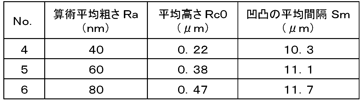
続けて、これら種々の表面状態を有する感光層の表面に、それぞれ表面層を形成した。ここで、表面層の最表面(露光の入射側の表面)は、平均高さRc0の感光層の露光の入射側の表面(感光層と表面層との界面)よりも平均高さRc1がいずれも小さいものであり、λ/(4×n1)未満の値であった。これにより、本開示の実施例であるNo.1~6の試料を作製した。
次に、端部の面取り加工および外周面の鏡面加工を行なった素管に対して、外周面への切削加工によって、表3に示す条件で、表面に規則的な繰り返しの凹凸形状を有する基体とした。また同様に、外周面へのブラスト処理によって、表4に示す条件で、表面に不規則な凹凸形状を有する基体とした。
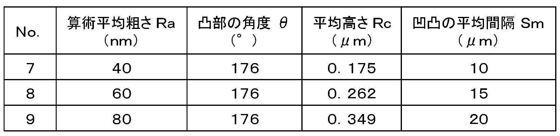

次に、これら基体をクリーンルーム内に搬入し、油分などを取り除く精密洗浄を経た後、図2に示す成膜装置の反応室にセットし、前述の成膜方法を用いて、基体の外周面に感光体層を形成した。感光体層における各層の構成は次の通りである。
阻止層は、a-SiにNおよびOを加えたa-Si系材料に、ドーパントとしてBを含有させたものであり、層厚は6μmとした。光導電層は、a-Siに、ドーパントとしてBを含有させたものであり、層厚は14μmとした。表面層は、第2表面層および第1表面層からなるものとした。第2表面層は、a-SiC系の非晶質材料からなる層とし、層厚は1μmとした。また、屈折率n2は1.9であった。第1表面層は、イソパラフィン系溶剤からなる層とし、層厚は2μmとした。また、屈折率n1は1.4であった。
これらの試料においては、第2表面層の表面(露光の入射側の表面)の平均高さRc2は、基体の表面の平均高さRcが反映されて、表3および表4に示すRcと同じ値であった。これら平均高さRc2は、静電潜像を形成するための露光の波長λが650nm(0.65μm)であるのに対してλ/(4×n1)が0.116μm(116nm)であることから、いずれもそれ以上の値であった。
一方、第1表面層の表面(露光の入射側の表面)の平均高さRc1は、それぞれいずれも第2表面層の表面の平均高さRc2よりも小さく、λ/(4×n1)未満の値であった。これにより、本開示の実施例であるNo.7~12の試料を作製した。
次に、上記の素管に対して端部の面取り加工および外周面の鏡面加工を行なって基体とした。この基体をクリーンルーム内に搬入し、油分などを取り除く精密洗浄を経た後、図2に示す成膜装置の反応室にセットし、前述の成膜方法を用いて、基体の外周面に感光体層を形成した。感光体層における各層の構成は次の通りである。
阻止層は、a-SiにNおよびOを加えたa-Si系材料に、ドーパントとしてBを含有させたものであり、層厚は6μmとした。光導電層は、a-Siに、ドーパントとしてBを含有させたものであり、層厚は14μmとした。この光導電層の屈折率n0は4.4であった。表面層は、a-SiC系の層からa-C系の層と連続的に変化させた構成とし、層厚は全体で1μmとした。この表面層の屈折率n1は1.8であった。
この感光層の表面(露光の入射側の表面)の平均高さRc0はλ/(4×n1)未満であり、表面層の最表面(露光の入射側の表面)の平均高さRc1は、λ/(4×n1)未満の値であったが、平均高さRc0の感光層の露光の入射側の表面(感光層と表面層との界面)よりも平均高さRc1がいずれも大きいものであった。これにより、本開示の比較例である試料を作製した。
以上の実施例および比較例の各試料の感光体による画像品質について、画像における干渉縞状の濃度むらの有無を以下の方法で評価した。各条件で得られた感光体をそれぞれ、レーザプリンタである京セラドキュメントソリューションズ株式会社製のカラー複合機TASKalfa 3550ciを改造した装置に組み込み、印画を実施した。その印画結果から画像における濃度むらの有無を観察して評価した。その結果、実施例であるNo.1~12の試料については実用上問題となる濃度むらは確認されなかったのに対して、比較例の試料では干渉縞状の濃度むらが確認された。
以上により、本開示によれば、感光体への潜像形成のためのレーザ光による露光に対して表面層における干渉縞の発生を抑制することができ、画像の干渉縞状の濃度むらの発生を抑制して良好な画像品質を維持することができることが確認できた。
本開示の第1の電子写真感光体によれば、導電性基体上に位置する感光層と、感光層上に位置する表面層とを有し、表面層の屈折率をn1、露光の入射側の表面層の平均高さをRc1とし、感光層の屈折率をn0、露光の入射側の感光層の平均高さをRc0としたとき、1<n1<n0であり、かつRc1<λ/(4×n1)≦Rc0であることから、感光層の表面(感光層と表面層との界面)と、表面層の表面との間での露光による干渉縞の発生を抑制することができるので、画像における干渉縞状の濃度むらの発生を抑制して良好な画像品質を維持することが可能となる。
本開示の第2の電子写真感光体によれば、導電性基体上に位置する感光層と、感光層上に位置する表面層とを有し、表面層は、感光層側に位置する第2表面層と、第2表面層上に位置する第1表面層とを有しており、第1表面層の屈折率をn1、露光の入射側の第1表面層の平均高さをRc1とし、第2表面層の屈折率をn2、露光の入射側の第2表面層の平均高さをRc2としたとき、1<n1<n2であり、かつRc1<λ/(4×n1)≦Rc2であることから、第2表面層の表面(第2表面層と第1表面層との界面)と、第1表面層の表面との間での露光による干渉縞の発生を抑制することができるので、画像における干渉縞状の濃度むらの発生を抑制して良好な画像品質を維持することが可能となる。
本開示の画像形成装置によれば、上述の本開示の電子写真感光体を備えることから、静電潜像を形成するために波長λの露光を電子写真感光体に走査して画像を形成したときに、干渉縞状の濃度むらの発生を抑制して良好な画像品質を維持することが可能となる。
以上、本開示の具体的な実施形態の例を示したが、本開示はこれに限定されるものではなく、本開示の思想から逸脱しない範囲内で種々の変更が可能である。
10…電子写真感光体(感光体)
10A…導電性基体(基体)
10B…感光体層
101…感光層
1011…光導電層
1012…阻止層
102…表面層
1021…第1表面層
1022…第2表面層
X……画像形成装置
10A…導電性基体(基体)
10B…感光体層
101…感光層
1011…光導電層
1012…阻止層
102…表面層
1021…第1表面層
1022…第2表面層
X……画像形成装置
Claims (6)
- 静電潜像を形成するために波長λの露光が走査される電子写真感光体であって、
導電性基体と、該導電性基体上に位置する感光層と、該感光層上に位置する表面層とを有し、前記表面層の屈折率をn1、前記露光の入射側の平均高さをRc1とし、前記感光層の屈折率をn0、前記露光の入射側の平均高さをRc0としたとき、1<n1<n0であり、かつRc1<λ/(4×n1)≦Rc0である電子写真感光体。 - 静電潜像を形成するために波長λの露光が走査される電子写真感光体であって、
導電性基体と、該導電性基体上に位置する感光層と、該感光層上に位置する表面層とを有し、該表面層は、前記感光層側に位置する第2表面層と、該第2表面層上に位置する第1表面層とを有し、前記第1表面層の屈折率をn1、前記露光の入射側の平均高さをRc1とし、前記第2表面層の屈折率をn2、前記露光の入射側の平均高さをRc2としたとき、1<n1<n2であり、かつRc1<λ/(4×n1)≦Rc2である電子写真感光体。 - 前記感光層は非晶質珪素材料を含み、前記波長λは680nm以下である請求項1または2に記載の電子写真感光体。
- 前記表面層は非晶質材料、樹脂または液体からなる請求項1に記載の電子写真感光体。
- 前記第1表面層は非晶質材料、樹脂または液体からなる請求項2に記載の電子写真感光体。
- 請求項1から5のいずれかに記載の電子写真感光体を備えることを特徴とする画像形成装置。
Applications Claiming Priority (2)
| Application Number | Priority Date | Filing Date | Title |
|---|---|---|---|
| JP2018-141268 | 2018-07-27 | ||
| JP2018141268 | 2018-07-27 |
Publications (1)
| Publication Number | Publication Date |
|---|---|
| WO2020022385A1 true WO2020022385A1 (ja) | 2020-01-30 |
Family
ID=69180500
Family Applications (1)
| Application Number | Title | Priority Date | Filing Date |
|---|---|---|---|
| PCT/JP2019/029040 Ceased WO2020022385A1 (ja) | 2018-07-27 | 2019-07-24 | 電子写真感光体および画像形成装置 |
Country Status (1)
| Country | Link |
|---|---|
| WO (1) | WO2020022385A1 (ja) |
Cited By (1)
| Publication number | Priority date | Publication date | Assignee | Title |
|---|---|---|---|---|
| US20230324819A1 (en) * | 2020-08-20 | 2023-10-12 | Hidetoshi Kami | Laminate, device using the same, and production methods thereof |
Citations (9)
| Publication number | Priority date | Publication date | Assignee | Title |
|---|---|---|---|---|
| JPS60247647A (ja) * | 1984-05-23 | 1985-12-07 | Canon Inc | 静電荷像形成方法 |
| JPS60254168A (ja) * | 1984-05-31 | 1985-12-14 | Canon Inc | 静電荷像形成方法 |
| JPS61163345A (ja) * | 1985-01-16 | 1986-07-24 | Canon Inc | 電子写真感光体 |
| JPS62163058A (ja) * | 1986-01-13 | 1987-07-18 | Canon Inc | 電子写真感光体 |
| JPS6385567A (ja) * | 1986-09-29 | 1988-04-16 | Ricoh Co Ltd | 電子写真感光体 |
| JPS63113461A (ja) * | 1986-05-13 | 1988-05-18 | Konica Corp | 電子写真感光体 |
| JPH04233546A (ja) * | 1990-06-21 | 1992-08-21 | Xerox Corp | 感光性映像部材の化粧板効果抑制装置及び方法 |
| JPH09166881A (ja) * | 1995-12-18 | 1997-06-24 | Fuji Xerox Co Ltd | 電子写真感光体及び電子写真装置 |
| JP2009230117A (ja) * | 2008-02-26 | 2009-10-08 | Fuji Xerox Co Ltd | 電子写真用感光体、並びにこれを用いた画像形成装置及びプロセスカートリッジ |
-
2019
- 2019-07-24 WO PCT/JP2019/029040 patent/WO2020022385A1/ja not_active Ceased
Patent Citations (9)
| Publication number | Priority date | Publication date | Assignee | Title |
|---|---|---|---|---|
| JPS60247647A (ja) * | 1984-05-23 | 1985-12-07 | Canon Inc | 静電荷像形成方法 |
| JPS60254168A (ja) * | 1984-05-31 | 1985-12-14 | Canon Inc | 静電荷像形成方法 |
| JPS61163345A (ja) * | 1985-01-16 | 1986-07-24 | Canon Inc | 電子写真感光体 |
| JPS62163058A (ja) * | 1986-01-13 | 1987-07-18 | Canon Inc | 電子写真感光体 |
| JPS63113461A (ja) * | 1986-05-13 | 1988-05-18 | Konica Corp | 電子写真感光体 |
| JPS6385567A (ja) * | 1986-09-29 | 1988-04-16 | Ricoh Co Ltd | 電子写真感光体 |
| JPH04233546A (ja) * | 1990-06-21 | 1992-08-21 | Xerox Corp | 感光性映像部材の化粧板効果抑制装置及び方法 |
| JPH09166881A (ja) * | 1995-12-18 | 1997-06-24 | Fuji Xerox Co Ltd | 電子写真感光体及び電子写真装置 |
| JP2009230117A (ja) * | 2008-02-26 | 2009-10-08 | Fuji Xerox Co Ltd | 電子写真用感光体、並びにこれを用いた画像形成装置及びプロセスカートリッジ |
Cited By (1)
| Publication number | Priority date | Publication date | Assignee | Title |
|---|---|---|---|---|
| US20230324819A1 (en) * | 2020-08-20 | 2023-10-12 | Hidetoshi Kami | Laminate, device using the same, and production methods thereof |
Similar Documents
| Publication | Publication Date | Title |
|---|---|---|
| JP4404942B2 (ja) | 画像形成装置 | |
| JP4377923B2 (ja) | 画像形成装置 | |
| JP5489426B2 (ja) | 電子写真感光体および該電子写真感光体を備える画像形成装置 | |
| WO2020022385A1 (ja) | 電子写真感光体および画像形成装置 | |
| JP4242901B2 (ja) | 画像形成装置 | |
| JP4996684B2 (ja) | 電子写真感光体およびその製造方法、並びに画像形成装置 | |
| JP2002229303A (ja) | 電子写真装置 | |
| JP3566621B2 (ja) | 電子写真感光体及びそれを用いた装置 | |
| JPWO2009028448A1 (ja) | 電子写真感光体および該電子写真感光体を備える画像形成装置 | |
| JP5517420B2 (ja) | 電子写真感光体および該電子写真感光体を備える画像形成装置 | |
| US7759034B2 (en) | Electrophotographic photosensitive member, method of producing the same and image forming apparatus | |
| JP4436823B2 (ja) | 画像形成装置 | |
| JP2019144476A (ja) | 電子写真感光体およびこれを備える画像形成装置 | |
| JP6962835B2 (ja) | 電子写真感光体およびこれを備える画像形成装置 | |
| JP3535664B2 (ja) | 電子写真装置 | |
| JP7766574B2 (ja) | 電子写真感光体および電子写真感光体の製造方法 | |
| JP4683637B2 (ja) | 電子写真感光体および電子写真装置 | |
| US9291981B2 (en) | Electrophotographic photoreceptor and image forming apparatus including the same | |
| JP4283331B2 (ja) | 画像形成装置 | |
| JP5436227B2 (ja) | 電子写真感光体、これを備えた画像形成装置および電子写真感光体の製造方法 | |
| JPH06186763A (ja) | 光受容部材、感光体の再生利用方法および表面処理方法 | |
| JPH08227260A (ja) | 電子写真装置の除湿装置 | |
| JP2007052242A (ja) | 電子写真感光体及びその製造方法 | |
| JP2009036932A (ja) | 電子写真感光体およびこれを備えた画像形成装置 | |
| JPH09311494A (ja) | 画像形成装置および画像形成装置用感光体 |
Legal Events
| Date | Code | Title | Description |
|---|---|---|---|
| 121 | Ep: the epo has been informed by wipo that ep was designated in this application |
Ref document number: 19842021 Country of ref document: EP Kind code of ref document: A1 |
|
| NENP | Non-entry into the national phase |
Ref country code: DE |
|
| 122 | Ep: pct application non-entry in european phase |
Ref document number: 19842021 Country of ref document: EP Kind code of ref document: A1 |
|
| NENP | Non-entry into the national phase |
Ref country code: JP |