WO2020008844A1 - 電気回路装置 - Google Patents
電気回路装置 Download PDFInfo
- Publication number
- WO2020008844A1 WO2020008844A1 PCT/JP2019/023809 JP2019023809W WO2020008844A1 WO 2020008844 A1 WO2020008844 A1 WO 2020008844A1 JP 2019023809 W JP2019023809 W JP 2019023809W WO 2020008844 A1 WO2020008844 A1 WO 2020008844A1
- Authority
- WO
- WIPO (PCT)
- Prior art keywords
- driver
- magnetic
- conductor
- electric circuit
- circuit device
- Prior art date
- Legal status (The legal status is an assumption and is not a legal conclusion. Google has not performed a legal analysis and makes no representation as to the accuracy of the status listed.)
- Ceased
Links
Images





Classifications
-
- H—ELECTRICITY
- H02—GENERATION; CONVERSION OR DISTRIBUTION OF ELECTRIC POWER
- H02M—APPARATUS FOR CONVERSION BETWEEN AC AND AC, BETWEEN AC AND DC, OR BETWEEN DC AND DC, AND FOR USE WITH MAINS OR SIMILAR POWER SUPPLY SYSTEMS; CONVERSION OF DC OR AC INPUT POWER INTO SURGE OUTPUT POWER; CONTROL OR REGULATION THEREOF
- H02M7/00—Conversion of AC power input into DC power output; Conversion of DC power input into AC power output
- H02M7/42—Conversion of DC power input into AC power output without possibility of reversal
- H02M7/44—Conversion of DC power input into AC power output without possibility of reversal by static converters
- H02M7/48—Conversion of DC power input into AC power output without possibility of reversal by static converters using discharge tubes with control electrode or semiconductor devices with control electrode
Definitions
- the present invention relates to an electric circuit device.
- a power conversion device that converts DC power supplied from a battery into AC power is known as an electric circuit device.
- a current sensor for detecting a current is arranged.
- a so-called coreless type current sensor which does not use an expensive magnetic flux collecting core having a relatively large volume has been adopted.
- a power conversion device having a coreless type current sensor is, for example, as described in Patent Document 1 below, a conductor formed of a bus bar, a current detection element that detects a current flowing through the bus bar, and a current detection element that is shielded from an external magnetic field. A magnetic shielding part.
- the present invention has been made to solve such a technical problem, and an object of the present invention is to provide an electric circuit device capable of reducing the influence of noise from a conductor and ensuring stable operation.
- An electric circuit device includes a switching circuit unit having a switching element, a driver circuit board having a mounting surface on which a driver IC that outputs a drive signal to the switching element is mounted, and an electric circuit electrically connected to the switching circuit unit.
- a long conductor to be connected a current detecting element for detecting a current flowing through the conductor, and a magnetic shielding portion for shielding the current detecting element from an external magnetic field, and
- the driver IC has at least a portion overlapping with the magnetic shielding portion, and / or a region on both sides of the magnetic shielding portion in a direction orthogonal to the longitudinal direction of the conductor. It is characterized in that they are arranged at overlapping positions.
- the magnetic shield since the magnetic shield is provided with the magnetic shield that shields the current detection element from the external magnetic field, the magnetic shield collects the magnetic flux generated by the current flowing through the conductor and stabilizes the distribution of the magnetic flux when the magnetic flux crosses the current detection element. By doing so, noise from the conductor can be reduced.
- the driver IC is disposed at a position where at least a part of the driver IC overlaps with the magnetic shielding portion or / and at a position where the driver IC overlaps the regions on both sides of the magnetic shielding portion in a direction orthogonal to the longitudinal direction of the conductor. Can reduce the influence of noise. As a result, malfunction of the driver IC due to noise can be prevented, and stable operation of the driver IC can be ensured.
- FIG. 2 is a sectional view taken along line AA in FIG. 1.
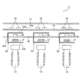
- FIG. 2 is a schematic cross-sectional view illustrating a structure of a power conversion device. It is a top view showing arrangement of an exchange bus bar.
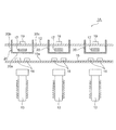
- FIG. 3 is a schematic diagram for explaining an arrangement position of a driver IC.
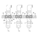
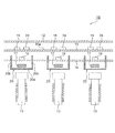
- FIG. 9 is a schematic diagram illustrating a modification of the arrangement position of the driver IC.
- FIG. 9 is a schematic diagram illustrating a modification of the arrangement position of the driver IC.
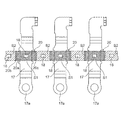
- FIG. 9 is a schematic diagram illustrating a modification of the arrangement position of the driver IC.
- FIG. 9 is a schematic diagram illustrating a modification of the arrangement position of the driver IC.
- FIG. 9 is a schematic diagram illustrating a modification of the arrangement position of the driver IC.
- FIG. 1 is a perspective view showing the power converter according to the first embodiment
- FIG. 2 is a cross-sectional view along the line AA in FIG.
- FIG. 3 is a schematic cross-sectional view showing the structure of the power converter
- FIG. 4 is a plan view showing the arrangement of the AC bus bars
- FIG. 5 is a schematic view for explaining the arrangement position of the driver IC.
- the power converter 1 of the present embodiment is used to convert DC power supplied from a battery into AC power and drive a motor or the like.
- the power conversion device 1 has a substantially rectangular parallelepiped shape, and is mounted on a case 10 in which a space for accommodating the switching circuit unit 14 and the driver circuit board 15 and the like is formed, and on an upper portion of the case 10 by screws.
- a metal base plate 11 and a control board 12 fixed above the metal base plate 11 are provided.
- a switching circuit unit 14 having a plurality of (here, six) switching elements 13 is accommodated in a lower portion of the case 10.
- the switching circuit unit 14 has a conversion circuit that converts DC power into AC power.
- the six switching elements 13 are arranged side by side at a certain interval in the left-right direction.
- a driver circuit board 15, a current sensor board 16, and a plurality (six in this case) of AC bus bars 17 are arranged in this order between the metal base plate 11 and the switching circuit section 14 from above to below. Have been.
- the driver circuit board 15 has a mounting surface 15a on which a plurality of (here, 12) driver ICs 18 are mounted.
- the driver IC 18 since the mounting surface 15 a is the upper surface of the driver circuit board 15, the driver IC 18 is to be mounted on the upper surface of the driver circuit board 15. May be implemented.
- the # 12 driver ICs 18 are arranged as a set of two so as to correspond to the six switching elements 13 described above. That is, two driver ICs 18 correspond to one switching element 13. These driver ICs 18 output drive signals to the corresponding switching elements 13.
- #Six AC bus bars 17 are arranged one-to-one with respect to six switching elements 13.
- Each of the AC busbars 17 corresponds to a “conductor” described in the claims, is electrically connected to the switching circuit unit 14, and has the U-phase of each of the two three-phase motors. AC power is transmitted to the V and W phases.
- the AC bus bar 17 is formed in a long shape by a metal plate such as aluminum, for example, and has one end connected to the switching circuit unit 14 and the other end connected to the output terminal unit 17 a projecting from the case 10.
- the six AC bus bars 17 are arranged side by side so that the width direction orthogonal to the longitudinal direction matches the direction in which the switching elements 13 are arranged.
- these AC bus bars 17 are integrally formed with a DC bus bar 25 for transmitting DC power by resin molding.
- the DC bus bar 25 corresponds to the “conductor” described in the claims, and is embedded in a resin mold.
- the DC bus bar 25 is formed in a long shape by a metal plate such as aluminum similarly to the AC bus bar 17, and is connected to a DC power supply terminal 26 protruding from the case 10.
- a current sensor board 16 on which six current detection elements 19 are mounted is arranged above the AC bus bar 17.
- the six current detection elements 19 are provided one-to-one with respect to the six AC bus bars 17, and are disposed immediately above the corresponding AC bus bars 17.
- the current detection element 19 includes, for example, a Hall element or a Hall IC as a magnetoelectric conversion element, detects a current flowing through the AC bus bar 17, and outputs the detected result to the control board 12.
- the current detection element 19 is mounted on the upper surface of the current sensor substrate 16, but may be mounted on the lower surface of the current sensor substrate 16 as needed.
- the power conversion device 1 includes the magnetic shielding unit 20 that shields each current detection element 19 from an external magnetic field.
- the magnetic shielding part 20 has a U-shaped cross section having an opening at the top, and is arranged so as to surround a part of the AC bus bar 17 and the current detecting element 19.
- the magnetic shielding portion 20 is located between the AC bus bar 17 and the switching element 13 and extends in the width direction of the AC bus bar 17, and stands upright from both ends of the bottom plate portion 20 a in the width direction of the AC bus bar 17. And a pair of side plate portions 20b and 20c facing each other.
- the driver circuit board 15 is disposed so as to face the opening of the magnetic shield 20.
- the side plate portions 20b and 20c of the magnetic shield portion 20 penetrate the current sensor board 16 and surround the bus bar 17 from both sides in the width direction of the bus bar 17 so as to surround the bus bar 17 between the driver circuit board 15 and the current sensor board 16.
- Extending to The magnetic shielding unit 20 having such a structure is formed by bending a metal plate such as a thin silicon steel plate, permalloy, or iron into a U-shape, and is integrated with the current sensor substrate 16 by a resin mold.
- the driver IC 18 when the driver IC 18 is viewed from the normal direction of the mounting surface 15 a of the driver circuit board 15, the driver IC 18 is disposed at a position where the entire driver IC 18 overlaps the magnetic shield 20. Specifically, as shown in FIG. 5, when the driver IC 18 is viewed from the normal direction of the mounting surface 15a of the driver circuit board 15 (that is, the driver IC 18 from above), the region of the magnetic shield 20 is the first region. At S1, the entire driver IC 18 overlaps the first area S1.
- the driver IC 18 is disposed at a position that entirely overlaps the first region S1.
- the influence of noise from the AC bus bar 17 can be reduced, and malfunction of the driver IC 18 due to the noise can be prevented. Therefore, even if the driver IC 18 is arranged at a position close to the AC bus bar 17, stable operation of the driver IC 18 can be ensured.
- the disposition position of the driver IC 18 is not limited to the position where the whole is overlapped with the first region S1 as described above.
- the driver IC 18 When the driver IC 18 is viewed from the normal direction of the mounting surface 15a of the driver circuit board 15, when the left and right regions sandwiching the magnetic shield 20 in the width direction of the AC bus bar 17 are defined as the second region S2, the driver IC 18 May be arranged at a position where at least a part thereof overlaps the first region S1 described above, and / or may be arranged at a position which overlaps the second region S2.
- two driver ICs 18 corresponding to the respective magnetic shields 20 are arranged near one end of the AC bus bar 17 in the magnetic shield 20 in the longitudinal direction.
- a part of the driver IC 18 overlaps the first area S1, and the other part does not overlap the first area S1. In such a case, the same operation and effect as the above-described embodiment can be obtained.
- two driver ICs 18 corresponding to the respective magnetic shields 20 are arranged near both ends of the AC bus bar 17 in the width direction of the magnetic shield 20. Specifically, one of the two driver ICs 18 is disposed at the left end of the magnetic shield 20, and the other is disposed at the right end of the magnetic shield 20. A part of the driver IC 18 overlaps the first area S1, and the other part overlaps the second area S2. In such a case, the same operation and effect as the above-described embodiment can be obtained.
- the two driver ICs 18 corresponding to the respective magnetic shields 20 are arranged at positions where the entirety overlaps the second region S2.
- the driver IC 18 is arranged at a position that overlaps with the region between the adjacent magnetic shields 20. In such a case, the same operation and effect as the above-described embodiment can be obtained.
- one of the two driver ICs 18 corresponding to each magnetic shielding unit 20 is disposed at a position where the whole thereof overlaps the first area S1, and the other is entirely the second area. It is arranged at a position overlapping S2. In such a case, the same operation and effect as those of the above embodiment can be obtained.
- the driver circuit board 15 may be arranged so as to face a portion other than the opening of the magnetic shield.
- the magnetic shielding portion 21 has a U-shaped cross section having an opening on the side (here, left side), and the top plate 21 a and the bottom plate 21 opposing each other in the up-down direction. It has a part 21b and a right side plate part 21c that connects the top plate part 21a and the bottom plate part 21b.
- the driver circuit board 15 is disposed above the top plate 21a so as to face the top plate 21a of the magnetic shielding unit 21.
- the magnetic shield 21 is formed of the same material as the magnetic shield 20 described above.
- the same operation and effect as those of the above-described embodiment can be obtained.
- the driver circuit board 15 is disposed so as to face a portion other than the opening of the magnetic shielding unit 21, the driver circuit board 15 Is less affected by the magnetic flux leaked from the opening as compared with the case where is disposed facing the opening of the magnetic shield. For this reason, the effect of reducing the influence of noise from the AC bus bar 17 can be further enhanced, and stable operation of the driver IC 18 can be more easily secured.
- the magnetic shield 22 has a U-shaped cross section having an opening on the side (here, right side), and the top plate 22a and the bottom plate 22 oppose each other in the vertical direction. It has a portion 22b and a left side plate portion 22c connecting the top plate portion 22a and the bottom plate portion 22b.
- the driver circuit board 15 is disposed above the top plate 22a so as to face the top plate 22a of the magnetic shielding unit 22.
- the magnetic shield 22 is formed of the same material as the magnetic shield 20 described above.
- the same operation and effect as those of the above-described embodiment can be obtained, and since the driver circuit board 15 is disposed so as to face a portion other than the opening of the magnetic shielding portion 22, the driver circuit board 15 Is less affected by the magnetic flux leaked from the opening as compared with the case where is disposed facing the opening of the magnetic shield. For this reason, the effect of reducing the influence of noise from the AC bus bar 17 can be further enhanced, and stable operation of the driver IC 18 can be more easily ensured.
- the magnetic shield 23 has a U-shaped cross section having an opening below, and a top plate 23 a extending in the width direction of the AC bus bar 17, and a top plate 23 a.
- the AC bus bar 17 has a pair of side plate portions 23b and 23c which are vertically provided from both ends in the width direction and face each other.
- the driver circuit board 15 is disposed above the top plate 23a so as to face the top plate 23a of the magnetic shielding unit 23.
- the magnetic shield 23 is formed of the same material as the magnetic shield 20 described above.
- the same operation and effect as those of the above-described embodiment can be obtained.
- the driver circuit board 15 is disposed so as to face a portion other than the opening of the magnetic shield 23, the driver circuit board 15 Is less affected by the magnetic flux leaked from the opening as compared with the case where is disposed facing the opening of the magnetic shield. For this reason, the effect of reducing the influence of noise from the AC bus bar 17 can be further enhanced, and stable operation of the driver IC 18 can be more easily secured.
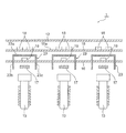
- FIG. 13 is a schematic cross-sectional view illustrating the power conversion device according to the second embodiment.
- the power converter 1A of the present embodiment is different from the above-described first embodiment in that the control board also functions as a current sensor board.
- the other structure is the same as that of the first embodiment, and the description thereof will not be repeated.
- the current detection element 19 is directly mounted on the control substrate 12. More specifically, the current detection element 19 is mounted on the control board 12 at a position immediately above the corresponding AC bus bar 17.
- the magnetic shield part 20 is integrated with the control board 12 by molding resin in a state where the side plate parts 20b and 20c penetrate the control board 12.
- the driver circuit board 15 on which the driver IC 18 is mounted is arranged below the magnetic shield 20 so as to face the bottom plate 20a of the magnetic shield 20.
- the same operation and effect as those of the above-described first embodiment can be obtained, and the number of components can be reduced by omitting the current sensor board, so that cost reduction and power consumption can be reduced.
- the thickness of the converter 1A can be reduced.
- the driver circuit board 15 is disposed so as to face a portion other than the opening of the magnetic shield 20, the driver circuit board 15 is disposed to face the opening of the magnetic shield. The effect of the magnetic flux leaked from the opening is reduced. Therefore, the effect of reducing the influence of noise from the AC bus bar 17 can be further enhanced.
- FIG. 14 is a schematic sectional view showing a power converter according to the third embodiment.
- the power converter 1B of the present embodiment differs from the above-described first embodiment in that a temperature IC is further mounted on a driver circuit board.
- the other structure is the same as that of the first embodiment, and the description thereof will not be repeated.
- one driver IC 18 and one temperature IC 24 are arranged for each switching element 13.
- the temperature IC 24 is mounted on the mounting surface 15 a of the driver circuit board 15 so as to be adjacent to the driver IC 18.
- the temperature IC 24 detects the temperature of the switching element 13 of the switching circuit unit 14 and outputs the detection result to the control board 12. Then, when the temperature IC 24 is viewed from the normal direction of the mounting surface 15a of the driver circuit board 15, the temperature IC 24 is arranged at a position where the entire temperature IC 24 overlaps the first region S1 like the driver IC 18.
- the same operation and effect as those of the above-described first embodiment can be obtained, and further, the following operation and effect can be obtained. That is, when the temperature IC 24 is viewed from the normal direction of the mounting surface 15 a of the driver circuit board 15, the temperature IC 24 is disposed at a position overlapping the first region S 1 as a whole. The influence on the IC 24 can be reduced. Therefore, stable operation of the temperature IC 24 can be ensured, and detection accuracy of the temperature IC 24 can be improved.
- the arrangement position of the temperature IC 24 is not limited to being arranged at a position where the entire temperature IC 24 overlaps the first region S1.
- the temperature IC 24 is viewed from the normal direction of the mounting surface 15a of the driver circuit board 15, at least a part of the temperature IC 24 may be arranged at a position overlapping the above-described first region S1, and / or It may be arranged at a position overlapping the area S2.
- the accuracy of motor control can be further improved by detecting the current value on the DC side in addition to the detection of the current value on the AC side.
Landscapes
- Engineering & Computer Science (AREA)
- Power Engineering (AREA)
- Inverter Devices (AREA)
Abstract
導体からのノイズの影響を低減し、安定した動作を確保できる電気回路装置を提供する。 電力変換装置1は、スイッチング素子13を有するスイッチング回路部14、ドライバIC18が実装される実装面15aを有するドライバ回路基板15、スイッチング回路部14と電気的に接続される長尺状の交流バスバー17、交流バスバー17に流れる電流を検出する電流検出素子19、電流検出素子19を外部磁界から遮蔽する磁気遮蔽部20を備える。実装面15aの法線方向からドライバIC18を見たときに、ドライバIC18は全体が磁気遮蔽部20と重なる位置に配置されている。
Description
本発明は、電気回路装置に関する。
電気回路装置として、バッテリから供給される直流電力を交流電力に変換する電力変換装置が知られている。このような電力変換装置において、電流を検出する電流センサが配置されている。最近では、電力変換装置の小型化及び低コスト化を図るために、体積が比較的大きく且つ高価な集磁コアを使わない、いわゆるコアレスタイプの電流センサの採用が進んでいる。コアレスタイプの電流センサを有する電力変換装置は、例えば下記特許文献1に記載のように、バスバーからなる導体と、バスバーに流れる電流を検出する電流検出素子と、電流検出素子を外部磁界から遮蔽する磁気遮蔽部とを備えている。
コアレスタイプの電流センサを採用することにより、電力変換装置の小型化及び低価格化を実現できる。しかし、小型化に伴ってドライバICを有するドライバ回路基板がバスバーに近接した位置に配置されることになるので、コアレストランスを内蔵したドライバICはバスバーからのノイズの影響を受け易くなる。このため、ドライバICの誤作動を引き起こし、ドライバICの安定した動作を確保し難い問題が生じている。
本発明は、このような技術課題を解決するためになされたものであって、導体からのノイズの影響を低減し、安定した動作を確保できる電気回路装置を提供することを目的とする。
本発明に係る電気回路装置は、スイッチング素子を有するスイッチング回路部と、前記スイッチング素子に駆動信号を出力するドライバICが実装される実装面を有するドライバ回路基板と、前記スイッチング回路部と電気的に接続される長尺状の導体と、前記導体に流れる電流を検出する電流検出素子と、前記電流検出素子を外部磁界から遮蔽する磁気遮蔽部と、を備え、前記実装面の法線方向から前記ドライバICを見たときに、前記ドライバICは、少なくとも一部が前記磁気遮蔽部と重なる位置、又は/及び、前記導体の長手方向と直交する方向において前記磁気遮蔽部を挟んで両側の領域と重なる位置に配置されていることを特徴とする。
本発明によれば、電流検出素子を外部磁界から遮蔽する磁気遮蔽部を備えるので、磁気遮蔽部は導体に流れる電流が発する磁束を集め、磁束が電流検出素子を横切るときに磁束の分布を安定させることにより、導体からのノイズを低減ことができる。そして、ドライバICは少なくとも一部が磁気遮蔽部と重なる位置、又は/及び、導体の長手方向と直交する方向において磁気遮蔽部を挟んで両側の領域と重なる位置に配置されることで、導体からのノイズの影響を低減することができる。その結果、ノイズによるドライバICの誤作動を防止することができ、ドライバICの安定した動作を確保することができる。
以下、図面を参照して本発明に係る電気回路装置の実施形態について説明する。ここでは、電気回路装置として電力変換装置の例を挙げて説明するが、本発明はこれに限定されるものではなく、電力変換装置以外の電気回路装置にも適用できる。また、以下の説明において、上下、左右の方向及び位置は、図面に表示された状態に対応する便宜的な方向及び位置であって、電力変換装置の姿勢や配置を限定するものではない。
[第1実施形態]
図1は第1実施形態に係る電力変換装置を示す斜視図であり、図2は図1のA-A線に沿う断面図である。図3は電力変換装置の構造を示す模式断面図であり、図4は交流バスバーの配置を示す平面図であり、図5はドライバICの配置位置を説明するための模式図である。本実施形態の電力変換装置1は、バッテリから供給される直流電力を交流電力に変換し、モータ等を駆動させるために用いられるものである。この電力変換装置1は、略直方体形状を呈しており、内部にスイッチング回路部14やドライバ回路基板15等を収容する空間が形成されたケース10と、ネジ止めでケース10の上部に取り付けられた金属ベース板11と、金属ベース板11の上方に固定される制御基板12とを備えている。
図1は第1実施形態に係る電力変換装置を示す斜視図であり、図2は図1のA-A線に沿う断面図である。図3は電力変換装置の構造を示す模式断面図であり、図4は交流バスバーの配置を示す平面図であり、図5はドライバICの配置位置を説明するための模式図である。本実施形態の電力変換装置1は、バッテリから供給される直流電力を交流電力に変換し、モータ等を駆動させるために用いられるものである。この電力変換装置1は、略直方体形状を呈しており、内部にスイッチング回路部14やドライバ回路基板15等を収容する空間が形成されたケース10と、ネジ止めでケース10の上部に取り付けられた金属ベース板11と、金属ベース板11の上方に固定される制御基板12とを備えている。
図2に示すように、ケース10の内部下方には、複数(ここでは、6個)のスイッチング素子13を有するスイッチング回路部14が収容されている。スイッチング回路部14は、直流電力を交流電力に変換する変換回路を有する。6個のスイッチング素子13は、一定の間隔を持って左右方向に沿って並設されている。そして、金属ベース板11とスイッチング回路部14との間には、上方から下方に向かってドライバ回路基板15、電流センサ基板16、複数本(ここでは、6本)の交流バスバー17がこの順に配置されている。
ドライバ回路基板15は、複数(ここでは、12個)のドライバIC18が実装される実装面15aを有する。本実施形態において、実装面15aがドライバ回路基板15の上面であるため、ドライバIC18はドライバ回路基板15の上面に実装されることになっているが、必要に応じてドライバ回路基板15の下面に実装されても良い。
12個のドライバIC18は、2つ一組として上述した6個のスイッチング素子13に対応するように配置されている。すなわち、1個のスイッチング素子13につき、2個のドライバIC18が対応するようになっている。これらのドライバIC18は、それぞれ対応するスイッチング素子13に駆動信号を出力する。
6本の交流バスバー17は、6個のスイッチング素子13に対して1対1で配置されている。これの交流バスバー17は、それぞれ特許請求の範囲に記載の「導体」に相当するものであって、スイッチング回路部14と電気的に接続されるとともに、2つの三相モータのそれぞれのU相、V相、W相に交流電力を伝達する。より具体的には、交流バスバー17は、例えばアルミニウム等の金属板によって長尺状に形成され、一端部がスイッチング回路部14と接続され、他端部がケース10から張り出す出力端子部17aを形成する。そして、6本の交流バスバー17は、長手方向と直交する幅方向がスイッチング素子13の並設方向と一致するように並設されている。
図4に示すように、これらの交流バスバー17は、直流電力を伝達する直流バスバー25と樹脂モールドで一体的に形成されている。直流バスバー25は、特許請求の範囲に記載の「導体」に相当するものであり、樹脂モールドに埋め込まれている。直流バスバー25は、交流バスバー17と同様にアルミニウム等の金属板によって長尺状に形成され、ケース10から突設された直流電源端子26と接続されている。
交流バスバー17の上方には、6個の電流検出素子19が実装された電流センサ基板16が配置されている。6個の電流検出素子19は、6本の交流バスバー17に対して1対1で設けられるとともに、対応する交流バスバー17の直上位置に配置されている。電流検出素子19は、例えば磁電変換素子としてのホール素子やホールICからなり、交流バスバー17に流れる電流を検出し、その検出した結果を制御基板12に出力する。なお、本実施形態において、電流検出素子19は、電流センサ基板16の上面に実装されているが、必要に応じて電流センサ基板16の下面に実装されても良い。
また、本実施形態では、電力変換装置1は、各電流検出素子19を外部磁界から遮蔽する磁気遮蔽部20を備えている。磁気遮蔽部20は、上方に開口部を有する断面コ字状を呈しており、交流バスバー17の一部と電流検出素子19とを取り囲むように配置されている。この磁気遮蔽部20は、交流バスバー17とスイッチング素子13との間に位置するとともに交流バスバー17の幅方向に延びる底板部20aと、底板部20aにおける交流バスバー17の幅方向の両端部から立設されて互いに対向する一対の側板部20b,20cとを有する。ドライバ回路基板15は、磁気遮蔽部20の開口部と対向するように配置されている。
磁気遮蔽部20の側板部20b,20cは、電流センサ基板16を貫通し、バスバー17の幅方向の両側から該バスバー17を囲むように、ドライバ回路基板15と電流センサ基板16との間の空間まで延びている。このような構造を有する磁気遮蔽部20は、例えば薄いケイ素鋼板、パーマロイ、鉄などの金属板をコ字状に折り曲げることで形成され、樹脂モールドで電流センサ基板16と一体化されている。
そして、電流が交流バスバー17の長手方向に沿って流れると、交流バスバー17の周囲に磁束が発生する。磁気遮蔽部20は、交流バスバー17の一部を取り囲むので、交流バスバー17に流れる電流が発する磁束を集め、磁束が電流検出素子19を横切るときに磁束の分布を安定させる。これによって、交流バスバー17からのノイズによる電流検出素子19への影響を低減することができる。電流検出素子19は、交流バスバー17の電流に比例する磁束を検知して、該磁束に比例した電流を検出値として制御基板12に出力する。このように交流バスバー17に流れる電流の値を制御基板12にフィードバックすることで、モータ制御を高精度に行うことが可能になる。
また、本実施形態において、ドライバ回路基板15の実装面15aの法線方向からドライバIC18を見たときに、ドライバIC18は、全体が磁気遮蔽部20と重なる位置に配置されている。具体的には、図5に示すように、ドライバ回路基板15の実装面15aの法線方向からドライバIC18(すなわち、上方からドライバIC18)を見た場合、磁気遮蔽部20の領域を第1領域S1としたときに、ドライバIC18の全体が第1領域S1と重なっている。
このように構成された電力変換装置1によれば、磁気遮蔽部20が交流バスバー17からのノイズを減らすことができるので、ドライバIC18はその全体が第1領域S1と重なる位置に配置されることで、交流バスバー17からのノイズの影響を低減し、ノイズに起因するドライバIC18の誤作動を防止することができる。従って、ドライバIC18が交流バスバー17に近接した位置に配置されても、ドライバIC18の安定した動作を確保することができる。
なお、本実施形態の電力変換装置1については、様々な変形例が考えられる。
[ドライバICの配置位置に関する変形例]
まず、ドライバIC18の配置位置については、上述のようにその全体が第1領域S1と重なる位置に配置されることに限定されない。ドライバ回路基板15の実装面15aの法線方向からドライバIC18を見た場合、交流バスバー17の幅方向において磁気遮蔽部20を挟んで左右両側の領域を第2領域S2としたときに、ドライバIC18は、少なくとも一部が上述の第1領域S1と重なる位置に配置されても良く、又は/及び、第2領域S2と重なる位置に配置されても良い。
まず、ドライバIC18の配置位置については、上述のようにその全体が第1領域S1と重なる位置に配置されることに限定されない。ドライバ回路基板15の実装面15aの法線方向からドライバIC18を見た場合、交流バスバー17の幅方向において磁気遮蔽部20を挟んで左右両側の領域を第2領域S2としたときに、ドライバIC18は、少なくとも一部が上述の第1領域S1と重なる位置に配置されても良く、又は/及び、第2領域S2と重なる位置に配置されても良い。
例えば図6に示す変形例では、各磁気遮蔽部20に対応する2個のドライバIC18は、それぞれ磁気遮蔽部20における交流バスバー17の長手方向の一端部付近に配置されている。ドライバIC18の一部は第1領域S1と重なり、他部分は第1領域S1と重ならないようになっている。このような場合においても、上述の実施形態と同様な作用効果を得られる。
また、図7に示す変形例では、各磁気遮蔽部20に対応する2個のドライバIC18は、磁気遮蔽部20における交流バスバー17の幅方向の両端部付近に配置されている。具体的には、2個のドライバIC18のうちの一方は磁気遮蔽部20の左端部、他方は磁気遮蔽部20の右端部に配置されている。そして、ドライバIC18の一部は第1領域S1と重なり、他部分は第2領域S2と重なるようになっている。このような場合においても、上述の実施形態と同様な作用効果を得られる。
また、図8に示す変形例では、各磁気遮蔽部20に対応する2個のドライバIC18は、それぞれの全体が第2領域S2と重なる位置に配置されている。換言すれば、ドライバIC18は、隣接する磁気遮蔽部20同士の間の領域と重なる位置に配置されている。このような場合においても、上述の実施形態と同様な作用効果を得られる。
また、図9に示す変形例では、各磁気遮蔽部20に対応する2個のドライバIC18のうちの一方はその全体が第1領域S1と重なる位置に配置され、他方はその全体が第2領域S2と重なる位置に配置されている。このような場合においても、上述の実施形態と同様な作用効果を得られる。
[磁気遮蔽部の形状に関する変形例]
次に、ドライバ回路基板15は、磁気遮蔽部の開口部以外の部分と対向するように配置されても良い。
次に、ドライバ回路基板15は、磁気遮蔽部の開口部以外の部分と対向するように配置されても良い。
例えば、図10に示す変形例では、磁気遮蔽部21は、側方(ここでは、左側)に開口部を有する断面コ字状を呈しており、上下方向において互いに対向する天板部21aと底板部21bと、天板部21a及び底板部21bを連結する右側板部21cとを有する。そして、ドライバ回路基板15は、磁気遮蔽部21の天板部21aと対向するように該天板部21aの上方に配置されている。なお、磁気遮蔽部21は、上述の磁気遮蔽部20と同じ材料によって形成されている。
本変形例によれば、上述の実施形態と同様な作用効果を得られるほか、ドライバ回路基板15は磁気遮蔽部21の開口部以外の部分と対向するように配置されるので、ドライバ回路基板15が磁気遮蔽部の開口部と対向して配置される場合と比べて、開口部から漏れた磁束の影響が少なくなる。このため、交流バスバー17からのノイズの影響低減効果を更に高めることができ、ドライバIC18の安定した動作をより確保し易くなる。
また、図11に示す変形例では、磁気遮蔽部22は、側方(ここでは、右側)に開口部を有する断面コ字状を呈しており、上下方向において互いに対向する天板部22aと底板部22bと、天板部22a及び底板部22bを連結する左側板部22cとを有する。そして、ドライバ回路基板15は、磁気遮蔽部22の天板部22aと対向するように該天板部22aの上方に配置されている。なお、磁気遮蔽部22は、上述の磁気遮蔽部20と同じ材料によって形成されている。
本変形例によれば、上述の実施形態と同様な作用効果を得られるほか、ドライバ回路基板15は磁気遮蔽部22の開口部以外の部分と対向するように配置されるので、ドライバ回路基板15が磁気遮蔽部の開口部と対向して配置される場合と比べて、開口部から漏れた磁束の影響が少なくなる。このため、交流バスバー17からのノイズの影響低減効果を更に高めることができ、ドライバIC18の安定した動作をより確保し易くなる。
また、図12に示す変形例では、磁気遮蔽部23は、下方に開口部を有する断面コ字状を呈しており、交流バスバー17の幅方向に延びる天板部23aと、天板部23aにおける交流バスバー17の幅方向の両端部から垂設されて互いに対向する一対の側板部23b,23cとを有する。そして、ドライバ回路基板15は、磁気遮蔽部23の天板部23aと対向するように該天板部23aの上方に配置されている。なお、磁気遮蔽部23は、上述の磁気遮蔽部20と同じ材料によって形成されている。
本変形例によれば、上述の実施形態と同様な作用効果を得られるほか、ドライバ回路基板15は磁気遮蔽部23の開口部以外の部分と対向するように配置されるので、ドライバ回路基板15が磁気遮蔽部の開口部と対向して配置される場合と比べて、開口部から漏れた磁束の影響が少なくなる。このため、交流バスバー17からのノイズの影響低減効果を更に高めることができ、ドライバIC18の安定した動作をより確保し易くなる。
[第2実施形態]
図13は第2実施形態に係る電力変換装置を示す模式断面図である。本実施形態の電力変換装置1Aは、制御基板が電流センサ基板の機能を兼ねる点において上述の第1実施形態と異なっている。その他の構造は第1実施形態と同様であるので、重複説明を省略する。
図13は第2実施形態に係る電力変換装置を示す模式断面図である。本実施形態の電力変換装置1Aは、制御基板が電流センサ基板の機能を兼ねる点において上述の第1実施形態と異なっている。その他の構造は第1実施形態と同様であるので、重複説明を省略する。
図13に示すように、本実施形態の電力変換装置1Aでは、電流センサ基板が設けられておらず、電流検出素子19が制御基板12に直接実装されている。より具体的には、電流検出素子19は、制御基板12において、対応する交流バスバー17の直上位置に実装されている。磁気遮蔽部20は、その側板部20b,20cが制御基板12を貫通した状態で、モールド樹脂によって制御基板12と一体化されている。一方、ドライバIC18が実装されたドライバ回路基板15は、磁気遮蔽部20の底板部20aと対向するように、磁気遮蔽部20の下方に配置されている。
このように構成された電力変換装置1Aによれば、上述の第1実施形態と同様な作用効果を得られるほか、電流センサ基板を省くことで、部品の点数が少なくなるので、コスト削減及び電力変換装置1Aの薄型化を図ることができる。更に、ドライバ回路基板15は磁気遮蔽部20の開口部以外の部分と対向するように配置されるので、ドライバ回路基板15が磁気遮蔽部の開口部と対向して配置される場合と比べて、開口部から漏れた磁束の影響が少なくなる。このため、交流バスバー17からのノイズの影響低減効果を更に高めることができる。
[第3実施形態]
図14は第3実施形態に係る電力変換装置を示す模式断面図である。本実施形態の電力変換装置1Bは、ドライバ回路基板に温度ICが更に実装される点において、上述の第1実施形態と異なっている。その他の構造は第1実施形態と同様であるので、重複説明を省略する。
図14は第3実施形態に係る電力変換装置を示す模式断面図である。本実施形態の電力変換装置1Bは、ドライバ回路基板に温度ICが更に実装される点において、上述の第1実施形態と異なっている。その他の構造は第1実施形態と同様であるので、重複説明を省略する。
図14に示すように、本実施形態の電力変換装置1Bでは、各スイッチング素子13に対してドライバIC18及び温度IC24が1つずつ配置されている。温度IC24は、ドライバ回路基板15の実装面15aにおいて、ドライバIC18と隣接して実装されている。この温度IC24は、スイッチング回路部14のスイッチング素子13の温度を検出し、その検出結果を制御基板12に出力する。そして、ドライバ回路基板15の実装面15aの法線方向から温度IC24を見たときに、温度IC24は、ドライバIC18と同様にその全体が第1領域S1と重なる位置に配置されている。
このように構成された電力変換装置1Bによれば、上述の第1実施形態と同様な作用効果を得られるほか、更に以下の作用効果を得られる。すなわち、ドライバ回路基板15の実装面15aの法線方向から温度IC24を見たときに、温度IC24はその全体が第1領域S1と重なる位置に配置されるので、交流バスバー17からのノイズによる温度IC24への影響を低減することができる。このため、温度IC24の安定した動作を確保することができ、温度IC24の検出精度を高めることができる。
なお、温度IC24の配置位置については、その全体が第1領域S1と重なる位置に配置されることに限定されない。ドライバ回路基板15の実装面15aの法線方向から温度IC24を見た場合、温度IC24は、少なくとも一部が上述の第1領域S1と重なる位置に配置されても良く、又は/及び、第2領域S2と重なる位置に配置されても良い。
以上、本発明の実施形態について詳述したが、本発明は、上述の実施形態に限定されるものではなく、特許請求の範囲に記載された本発明の精神を逸脱しない範囲で、種々の設計変更を行うことができるものである。例えば、上述の第1実施形態において、1個のスイッチング素子13につき2個のドライバIC18が対応するように配置される例を説明したが、1個のスイッチング素子13に対応するドライバIC18の数を適宜増減しても良い。
また、上述の実施形態では、交流バスバー17に流れる電流を検出する電流検出素子19が設けられる例を説明したが、直流バスバー25に流れる電流を検出する電流検出素子が更に設けられても良い。このようにすれば、交流側の電流値の検出に加えて直流側の電流値も検出することで、モータ制御の精度を一層高めることができる。
1,1A,1B 電力変換装置
10 ケース
11 金属ベース板
12 制御基板
13 スイッチング素子
14 スイッチング回路部
15 ドライバ回路基板
15a 実装面
16 電流センサ基板
17 交流バスバー(導体)
17a 出力端子部
18 ドライバIC
19 電流検出素子
20,21,22,23 磁気遮蔽部
20a,21b,22b 底板部
20b,20c,23b,23c 側板部
21a,22a,23a 天板部
21c 右側板部
22c 左側板部
24 温度IC
25 直流バスバー(導体)
26 直流電源端子
10 ケース
11 金属ベース板
12 制御基板
13 スイッチング素子
14 スイッチング回路部
15 ドライバ回路基板
15a 実装面
16 電流センサ基板
17 交流バスバー(導体)
17a 出力端子部
18 ドライバIC
19 電流検出素子
20,21,22,23 磁気遮蔽部
20a,21b,22b 底板部
20b,20c,23b,23c 側板部
21a,22a,23a 天板部
21c 右側板部
22c 左側板部
24 温度IC
25 直流バスバー(導体)
26 直流電源端子
Claims (7)
- スイッチング素子を有するスイッチング回路部と、
前記スイッチング素子に駆動信号を出力するドライバICが実装される実装面を有するドライバ回路基板と、
前記スイッチング回路部と電気的に接続される長尺状の導体と、
前記導体に流れる電流を検出する電流検出素子と、
前記電流検出素子を外部磁界から遮蔽する磁気遮蔽部と、
を備え、
前記実装面の法線方向から前記ドライバICを見たときに、前記ドライバICは、少なくとも一部が前記磁気遮蔽部と重なる位置、又は/及び、前記導体の長手方向と直交する方向において前記磁気遮蔽部を挟んで両側の領域と重なる位置に配置されていることを特徴とする電気回路装置。 - 前記実装面の法線方向から前記ドライバICを見たときに、前記ドライバICは、全体が前記磁気遮蔽部と重なる位置に配置されている請求項1に記載の電気回路装置。
- 前記磁気遮蔽部は、開口部を有し、
前記ドライバ回路基板は、前記磁気遮蔽部の前記開口部以外の部分と対向するように配置されている請求項1又は2に記載の電気回路装置。 - 前記ドライバ回路基板の前記実装面には、前記スイッチング回路部の温度を検出する温度ICが更に実装され、
前記実装面の法線方向から前記温度ICを見たときに、前記温度ICは、少なくとも一部が前記磁気遮蔽部と重なる位置、又は/及び、前記導体の長手方向と直交する方向において前記磁気遮蔽部を挟んで両側の領域と重なる位置に配置されている請求項1~3のいずれか一項に記載の電気回路装置。 - 前記スイッチング回路部は、直流電力を交流電力に変換する変換回路を有し、
前記導体は、前記交流電力を伝達する交流バスバーである請求項1~4のいずれか一項に記載の電気回路装置。 - 前記スイッチング回路部は、直流電力を交流電力に変換する変換回路を有し、
前記導体は、前記直流電力を伝達する直流バスバーである請求項1~5のいずれか一項に記載の電気回路装置。 - 前記導体は、複数であり、該導体の長手方向と直交する方向に沿って並設され、
前記磁気遮蔽部は、複数であり、前記複数の導体に対して1対1で設けられるとともに前記導体の並設方向に沿って配置され、
前記実装面の法線方向から前記ドライバICを見たときに、前記ドライバICは、隣接する前記磁気遮蔽部同士の間の領域と重なる位置に配置されている請求項1~6のいずれか一項に記載の電気回路装置。
Priority Applications (2)
| Application Number | Priority Date | Filing Date | Title |
|---|---|---|---|
| CN201980041935.5A CN112368929B (zh) | 2018-07-04 | 2019-06-17 | 电路装置 |
| JP2020528765A JP7000572B2 (ja) | 2018-07-04 | 2019-06-17 | 電気回路装置 |
Applications Claiming Priority (2)
| Application Number | Priority Date | Filing Date | Title |
|---|---|---|---|
| JP2018127812 | 2018-07-04 | ||
| JP2018-127812 | 2018-07-04 |
Publications (1)
| Publication Number | Publication Date |
|---|---|
| WO2020008844A1 true WO2020008844A1 (ja) | 2020-01-09 |
Family
ID=69060121
Family Applications (1)
| Application Number | Title | Priority Date | Filing Date |
|---|---|---|---|
| PCT/JP2019/023809 Ceased WO2020008844A1 (ja) | 2018-07-04 | 2019-06-17 | 電気回路装置 |
Country Status (3)
| Country | Link |
|---|---|
| JP (1) | JP7000572B2 (ja) |
| CN (1) | CN112368929B (ja) |
| WO (1) | WO2020008844A1 (ja) |
Cited By (2)
| Publication number | Priority date | Publication date | Assignee | Title |
|---|---|---|---|---|
| WO2021213698A1 (de) * | 2020-04-20 | 2021-10-28 | Tdk-Micronas Gmbh | Stromsensoreinheit |
| JP2023012919A (ja) * | 2021-07-14 | 2023-01-26 | 日立Astemo株式会社 | 電力変換装置 |
Citations (6)
| Publication number | Priority date | Publication date | Assignee | Title |
|---|---|---|---|---|
| JP2012065431A (ja) * | 2010-09-15 | 2012-03-29 | Aisin Aw Co Ltd | インバータ装置 |
| WO2012160876A1 (ja) * | 2011-05-20 | 2012-11-29 | 本田技研工業株式会社 | コアレス電流センサ構造体、コアレス電流センサ及び電流検知方法 |
| JP2015135288A (ja) * | 2014-01-17 | 2015-07-27 | 株式会社デンソー | 電流センサ |
| JP2017085883A (ja) * | 2015-02-25 | 2017-05-18 | 日立オートモティブシステムズ株式会社 | 半導体モジュール及びこれを備えた電力変換装置 |
| WO2018100778A1 (ja) * | 2016-12-01 | 2018-06-07 | 株式会社村田製作所 | 電流センサ及び電流センサユニット |
| JP2018096794A (ja) * | 2016-12-12 | 2018-06-21 | 株式会社デンソー | 電流センサ |
Family Cites Families (7)
| Publication number | Priority date | Publication date | Assignee | Title |
|---|---|---|---|---|
| JP5482736B2 (ja) * | 2011-06-28 | 2014-05-07 | 株式会社デンソー | 電流センサ |
| JP6350785B2 (ja) * | 2013-09-03 | 2018-07-04 | Tdk株式会社 | インバータ装置 |
| JP5840669B2 (ja) * | 2013-12-17 | 2016-01-06 | 株式会社デンソー | 電力変換装置 |
| JP6477089B2 (ja) * | 2014-05-23 | 2019-03-06 | 株式会社デンソー | 電流センサ付バスバーモジュール |
| US20180017656A1 (en) * | 2015-02-06 | 2018-01-18 | Hitachi Automotive Systems, Ltd. | Electric current sensor |
| WO2017217267A1 (ja) * | 2016-06-15 | 2017-12-21 | 株式会社デンソー | 電流センサ |
| JP6607172B2 (ja) * | 2016-11-17 | 2019-11-20 | 株式会社デンソー | 電流センサ装置 |
-
2019
- 2019-06-17 JP JP2020528765A patent/JP7000572B2/ja active Active
- 2019-06-17 CN CN201980041935.5A patent/CN112368929B/zh active Active
- 2019-06-17 WO PCT/JP2019/023809 patent/WO2020008844A1/ja not_active Ceased
Patent Citations (6)
| Publication number | Priority date | Publication date | Assignee | Title |
|---|---|---|---|---|
| JP2012065431A (ja) * | 2010-09-15 | 2012-03-29 | Aisin Aw Co Ltd | インバータ装置 |
| WO2012160876A1 (ja) * | 2011-05-20 | 2012-11-29 | 本田技研工業株式会社 | コアレス電流センサ構造体、コアレス電流センサ及び電流検知方法 |
| JP2015135288A (ja) * | 2014-01-17 | 2015-07-27 | 株式会社デンソー | 電流センサ |
| JP2017085883A (ja) * | 2015-02-25 | 2017-05-18 | 日立オートモティブシステムズ株式会社 | 半導体モジュール及びこれを備えた電力変換装置 |
| WO2018100778A1 (ja) * | 2016-12-01 | 2018-06-07 | 株式会社村田製作所 | 電流センサ及び電流センサユニット |
| JP2018096794A (ja) * | 2016-12-12 | 2018-06-21 | 株式会社デンソー | 電流センサ |
Cited By (3)
| Publication number | Priority date | Publication date | Assignee | Title |
|---|---|---|---|---|
| WO2021213698A1 (de) * | 2020-04-20 | 2021-10-28 | Tdk-Micronas Gmbh | Stromsensoreinheit |
| JP2023012919A (ja) * | 2021-07-14 | 2023-01-26 | 日立Astemo株式会社 | 電力変換装置 |
| JP7623904B2 (ja) | 2021-07-14 | 2025-01-29 | 日立Astemo株式会社 | 電力変換装置 |
Also Published As
| Publication number | Publication date |
|---|---|
| JPWO2020008844A1 (ja) | 2021-06-24 |
| JP7000572B2 (ja) | 2022-01-19 |
| CN112368929A (zh) | 2021-02-12 |
| CN112368929B (zh) | 2024-04-16 |
Similar Documents
| Publication | Publication Date | Title |
|---|---|---|
| CN106461706B (zh) | 电流检测装置 | |
| US9431776B2 (en) | Connector | |
| JP5699993B2 (ja) | インバータ | |
| JP2005321206A (ja) | 電流検出装置 | |
| JP2016173306A (ja) | バスバモジュール | |
| JP5556599B2 (ja) | 電力変換装置 | |
| JP6043977B2 (ja) | 分電盤 | |
| JP7000572B2 (ja) | 電気回路装置 | |
| JP6536553B2 (ja) | 電流センサ | |
| JP2016099111A (ja) | 電流センサ | |
| JP5859273B2 (ja) | 分電盤 | |
| JP5945975B2 (ja) | バスバモジュール | |
| JP6237525B2 (ja) | 電流センサ | |
| JP6979369B2 (ja) | 電力変換装置 | |
| JP6083017B2 (ja) | 電流計測用アダプタ | |
| WO2019069763A1 (ja) | 電流センサ | |
| JP2020005367A (ja) | 電力変換装置 | |
| JP2014055839A (ja) | 電流検出装置 | |
| JP6083018B2 (ja) | 電流計測部材 | |
| JP2600339Y2 (ja) | 回路遮断器および回路遮断器装着型電力量計 | |
| JP2016065791A (ja) | 電流検出装置 | |
| JP2008128915A (ja) | 電流測定装置および電流測定機能を備える半導体モジュール | |
| JP6878083B2 (ja) | 電流検出装置 | |
| US20260050013A1 (en) | Coreless current sensor module, current sensor module, and power module | |
| JP2011209256A (ja) | 多相電流の検出装置 |
Legal Events
| Date | Code | Title | Description |
|---|---|---|---|
| 121 | Ep: the epo has been informed by wipo that ep was designated in this application |
Ref document number: 19830389 Country of ref document: EP Kind code of ref document: A1 |
|
| ENP | Entry into the national phase |
Ref document number: 2020528765 Country of ref document: JP Kind code of ref document: A |
|
| NENP | Non-entry into the national phase |
Ref country code: DE |
|
| 122 | Ep: pct application non-entry in european phase |
Ref document number: 19830389 Country of ref document: EP Kind code of ref document: A1 |