WO2019239762A1 - Procédé de régulation de densité de défauts dans un substrat monocristallin de silicium - Google Patents
Procédé de régulation de densité de défauts dans un substrat monocristallin de silicium Download PDFInfo
- Publication number
- WO2019239762A1 WO2019239762A1 PCT/JP2019/019004 JP2019019004W WO2019239762A1 WO 2019239762 A1 WO2019239762 A1 WO 2019239762A1 JP 2019019004 W JP2019019004 W JP 2019019004W WO 2019239762 A1 WO2019239762 A1 WO 2019239762A1
- Authority
- WO
- WIPO (PCT)
- Prior art keywords
- single crystal
- silicon single
- crystal substrate
- defect density
- heat treatment
- Prior art date
Links
- XUIMIQQOPSSXEZ-UHFFFAOYSA-N Silicon Chemical compound [Si] XUIMIQQOPSSXEZ-UHFFFAOYSA-N 0.000 title claims abstract description 196
- 229910052710 silicon Inorganic materials 0.000 title claims abstract description 194
- 239000010703 silicon Substances 0.000 title claims abstract description 194
- 239000013078 crystal Substances 0.000 title claims abstract description 191
- 239000000758 substrate Substances 0.000 title claims abstract description 166
- 230000007547 defect Effects 0.000 title claims abstract description 117
- 238000000034 method Methods 0.000 title claims abstract description 108
- IJGRMHOSHXDMSA-UHFFFAOYSA-N Atomic nitrogen Chemical compound N#N IJGRMHOSHXDMSA-UHFFFAOYSA-N 0.000 claims abstract description 222
- 229910052757 nitrogen Inorganic materials 0.000 claims abstract description 114
- 238000010438 heat treatment Methods 0.000 claims abstract description 64
- 239000002245 particle Substances 0.000 claims abstract description 43
- 238000012360 testing method Methods 0.000 claims abstract description 25
- 238000002360 preparation method Methods 0.000 claims abstract description 12
- 238000005259 measurement Methods 0.000 claims abstract description 11
- 230000001678 irradiating effect Effects 0.000 claims abstract description 7
- 229910052760 oxygen Inorganic materials 0.000 claims description 59
- QVGXLLKOCUKJST-UHFFFAOYSA-N atomic oxygen Chemical compound [O] QVGXLLKOCUKJST-UHFFFAOYSA-N 0.000 claims description 58
- 239000001301 oxygen Substances 0.000 claims description 58
- OKTJSMMVPCPJKN-UHFFFAOYSA-N Carbon Chemical compound [C] OKTJSMMVPCPJKN-UHFFFAOYSA-N 0.000 claims description 35
- 229910052799 carbon Inorganic materials 0.000 claims description 35
- 238000005136 cathodoluminescence Methods 0.000 claims description 26
- 238000005424 photoluminescence Methods 0.000 claims description 15
- 239000002131 composite material Substances 0.000 claims description 9
- 238000004519 manufacturing process Methods 0.000 abstract description 7
- 238000010894 electron beam technology Methods 0.000 description 34
- 238000011084 recovery Methods 0.000 description 21
- 229910052720 vanadium Inorganic materials 0.000 description 15
- 230000006798 recombination Effects 0.000 description 14
- 238000005215 recombination Methods 0.000 description 13
- 101100060033 Drosophila melanogaster cic gene Proteins 0.000 description 12
- 101100060035 Mus musculus Cic gene Proteins 0.000 description 12
- 125000004429 atom Chemical group 0.000 description 12
- 239000002994 raw material Substances 0.000 description 12
- 239000012535 impurity Substances 0.000 description 11
- 230000001133 acceleration Effects 0.000 description 7
- 239000004065 semiconductor Substances 0.000 description 7
- 238000006243 chemical reaction Methods 0.000 description 5
- 230000000052 comparative effect Effects 0.000 description 5
- 239000002019 doping agent Substances 0.000 description 5
- 238000000295 emission spectrum Methods 0.000 description 5
- 229910021420 polycrystalline silicon Inorganic materials 0.000 description 5
- 230000007423 decrease Effects 0.000 description 4
- 238000002474 experimental method Methods 0.000 description 3
- 229910052698 phosphorus Inorganic materials 0.000 description 3
- ZOXJGFHDIHLPTG-UHFFFAOYSA-N Boron Chemical compound [B] ZOXJGFHDIHLPTG-UHFFFAOYSA-N 0.000 description 2
- OAICVXFJPJFONN-UHFFFAOYSA-N Phosphorus Chemical compound [P] OAICVXFJPJFONN-UHFFFAOYSA-N 0.000 description 2
- 230000004913 activation Effects 0.000 description 2
- 229910052796 boron Inorganic materials 0.000 description 2
- 239000000969 carrier Substances 0.000 description 2
- 238000005520 cutting process Methods 0.000 description 2
- 230000001419 dependent effect Effects 0.000 description 2
- 239000007789 gas Substances 0.000 description 2
- 239000001257 hydrogen Substances 0.000 description 2
- 229910052739 hydrogen Inorganic materials 0.000 description 2
- 125000004435 hydrogen atom Chemical class [H]* 0.000 description 2
- 238000005468 ion implantation Methods 0.000 description 2
- 238000004020 luminiscence type Methods 0.000 description 2
- 239000000463 material Substances 0.000 description 2
- 229910021421 monocrystalline silicon Inorganic materials 0.000 description 2
- 239000011574 phosphorus Substances 0.000 description 2
- FSLGCYNKXXIWGJ-UHFFFAOYSA-N silicon(1+) Chemical compound [Si+] FSLGCYNKXXIWGJ-UHFFFAOYSA-N 0.000 description 2
- 239000000126 substance Substances 0.000 description 2
- 229910052581 Si3N4 Inorganic materials 0.000 description 1
- 238000010521 absorption reaction Methods 0.000 description 1
- 230000015572 biosynthetic process Effects 0.000 description 1
- 238000003486 chemical etching Methods 0.000 description 1
- 239000000470 constituent Substances 0.000 description 1
- 230000000694 effects Effects 0.000 description 1
- 238000011156 evaluation Methods 0.000 description 1
- 230000005284 excitation Effects 0.000 description 1
- 230000005524 hole trap Effects 0.000 description 1
- 238000005498 polishing Methods 0.000 description 1
- 238000001004 secondary ion mass spectrometry Methods 0.000 description 1
- HQVNEWCFYHHQES-UHFFFAOYSA-N silicon nitride Chemical compound N12[Si]34N5[Si]62N3[Si]51N64 HQVNEWCFYHHQES-UHFFFAOYSA-N 0.000 description 1
Images


Classifications
-
- H—ELECTRICITY
- H01—ELECTRIC ELEMENTS
- H01L—SEMICONDUCTOR DEVICES NOT COVERED BY CLASS H10
- H01L21/00—Processes or apparatus adapted for the manufacture or treatment of semiconductor or solid state devices or of parts thereof
- H01L21/02—Manufacture or treatment of semiconductor devices or of parts thereof
- H01L21/04—Manufacture or treatment of semiconductor devices or of parts thereof the devices having potential barriers, e.g. a PN junction, depletion layer or carrier concentration layer
- H01L21/18—Manufacture or treatment of semiconductor devices or of parts thereof the devices having potential barriers, e.g. a PN junction, depletion layer or carrier concentration layer the devices having semiconductor bodies comprising elements of Group IV of the Periodic Table or AIIIBV compounds with or without impurities, e.g. doping materials
- H01L21/26—Bombardment with radiation
- H01L21/263—Bombardment with radiation with high-energy radiation
-
- C—CHEMISTRY; METALLURGY
- C30—CRYSTAL GROWTH
- C30B—SINGLE-CRYSTAL GROWTH; UNIDIRECTIONAL SOLIDIFICATION OF EUTECTIC MATERIAL OR UNIDIRECTIONAL DEMIXING OF EUTECTOID MATERIAL; REFINING BY ZONE-MELTING OF MATERIAL; PRODUCTION OF A HOMOGENEOUS POLYCRYSTALLINE MATERIAL WITH DEFINED STRUCTURE; SINGLE CRYSTALS OR HOMOGENEOUS POLYCRYSTALLINE MATERIAL WITH DEFINED STRUCTURE; AFTER-TREATMENT OF SINGLE CRYSTALS OR A HOMOGENEOUS POLYCRYSTALLINE MATERIAL WITH DEFINED STRUCTURE; APPARATUS THEREFOR
- C30B13/00—Single-crystal growth by zone-melting; Refining by zone-melting
-
- C—CHEMISTRY; METALLURGY
- C30—CRYSTAL GROWTH
- C30B—SINGLE-CRYSTAL GROWTH; UNIDIRECTIONAL SOLIDIFICATION OF EUTECTIC MATERIAL OR UNIDIRECTIONAL DEMIXING OF EUTECTOID MATERIAL; REFINING BY ZONE-MELTING OF MATERIAL; PRODUCTION OF A HOMOGENEOUS POLYCRYSTALLINE MATERIAL WITH DEFINED STRUCTURE; SINGLE CRYSTALS OR HOMOGENEOUS POLYCRYSTALLINE MATERIAL WITH DEFINED STRUCTURE; AFTER-TREATMENT OF SINGLE CRYSTALS OR A HOMOGENEOUS POLYCRYSTALLINE MATERIAL WITH DEFINED STRUCTURE; APPARATUS THEREFOR
- C30B29/00—Single crystals or homogeneous polycrystalline material with defined structure characterised by the material or by their shape
- C30B29/02—Elements
- C30B29/06—Silicon
-
- H—ELECTRICITY
- H01—ELECTRIC ELEMENTS
- H01L—SEMICONDUCTOR DEVICES NOT COVERED BY CLASS H10
- H01L22/00—Testing or measuring during manufacture or treatment; Reliability measurements, i.e. testing of parts without further processing to modify the parts as such; Structural arrangements therefor
- H01L22/10—Measuring as part of the manufacturing process
- H01L22/12—Measuring as part of the manufacturing process for structural parameters, e.g. thickness, line width, refractive index, temperature, warp, bond strength, defects, optical inspection, electrical measurement of structural dimensions, metallurgic measurement of diffusions
-
- H—ELECTRICITY
- H01—ELECTRIC ELEMENTS
- H01L—SEMICONDUCTOR DEVICES NOT COVERED BY CLASS H10
- H01L22/00—Testing or measuring during manufacture or treatment; Reliability measurements, i.e. testing of parts without further processing to modify the parts as such; Structural arrangements therefor
- H01L22/20—Sequence of activities consisting of a plurality of measurements, corrections, marking or sorting steps
Definitions
- the present invention relates to a method for controlling the defect density in a silicon single crystal substrate.
- particle beam irradiation and heat treatment are frequently performed.
- a high concentration dopant is ion-implanted, and the subsequent heat treatment activates the dopant and recovers damage caused by the ion implantation.
- defects that become the recombination centers of carriers are intentionally introduced by irradiation with particle beams such as electron beams and protons, and then the recombination lifetime is achieved by heat treatment. Make adjustments.
- Non-Patent Documents 1 to 4 there is a problem that device characteristics vary even if the conditions of particle beam irradiation and the conditions of heat treatment after particle beam irradiation are the same. As a variation factor of device characteristics, some substance contained in the silicon substrate itself is suspected as a factor, and there is a concern about the influence of impurities such as carbon and oxygen.
- Non-Patent Document 1 points out a problem that wafer dependence may occur in switching loss even when the same recombination lifetime control is performed, and main defects (CsI, CiCs, or CiOi generated by electron beam irradiation) are pointed out. ), The activation energy of only CiOi is dependent on the wafer, and the activation energy tends to increase when the oxygen concentration is high, so that oxygen impurities are considered to be a factor dependent on the wafer (however, Cs: substitutional carbon, Ci: interstitial carbon, Oi: interstitial oxygen, I: interstitial silicon). Further, in Non-Patent Document 2 and Non-Patent Document 3, when heat treatment is performed at 350 ° C. ⁇ 10 ° C.
- Non-Patent Document 4 in the improvement of the recovery characteristics of FWD (Free Wheeling Diode), when a crystal defect is locally introduced at a level equal to or higher than the donor concentration as in He irradiation, the CiOi functioning as a hole trap is used. It is described that density control is important, and that carbon concentration control is important. In such a case, it is necessary to control the density of the light element composite so as not to vary as much as possible.
- the density of the light element complex formed by particle beam irradiation and heat treatment is the constituent element of the light element complex. It is thought that it can be controlled by controlling the concentration of carbon and oxygen, but this is not always the case, and even if the carbon concentration and oxygen concentration are the same, the density of the light element complex may vary was there.
- the present invention has been made in view of the above-described problems, and can reduce variation in defect density caused by a silicon single crystal substrate in a device manufacturing process in which defect density is controlled by particle beam irradiation and heat treatment.
- An object of the present invention is to provide a method for controlling the defect density in a silicon single crystal substrate capable of controlling the defect density with high accuracy.
- the present invention has been made to solve the above-mentioned object, Preparing a silicon single crystal substrate for controlling the defect density; A particle beam irradiation step of irradiating the prepared silicon single crystal substrate with a particle beam; A method of controlling a defect density in the silicon single crystal substrate, wherein the silicon single crystal substrate is subjected to a heat treatment step after the particle beam irradiation step.
- a plurality of test silicon single crystal substrates having different nitrogen concentrations are irradiated with the particle beam in advance, and then heat treatment is performed to determine defect densities generated in the plurality of test silicon single crystal substrates.
- a method for controlling the defect density in a silicon single crystal substrate is provided.
- the defect targeted for controlling the defect density is carbon or a composite containing carbon and oxygen.
- the defect density is adjusted by adjusting the nitrogen concentration of the silicon single crystal substrate based on the correlation between the nitrogen concentration after the heat treatment step or the concentration of carbon or a complex containing carbon and oxygen. By controlling this, variation in defect density due to the silicon single crystal substrate can be reduced.
- the measurement step it is preferable to use a cathodoluminescence method or a photoluminescence method as a method of measuring the defect density.
- G-rays or C-rays that are emission lines derived from carbon or a composite containing carbon and oxygen can be observed.
- a cathodoluminescence method or a photoluminescence method can be suitably used.
- the silicon single crystal substrate to be prepared is manufactured from a nitrogen-added silicon single crystal grown by a floating zone method (FZ method).
- FZ method floating zone method
- FZ silicon single crystal substrates nitrogen is often added during crystal growth in order to reduce crystal defects introduced during crystal growth and improve wafer strength.
- concentration of nitrogen introduced into the grown single crystal can be controlled by adjusting the atmospheric gas during crystal growth.
- the defect density can be controlled by adjusting the nitrogen concentration of the silicon single crystal substrate based on the correlation between the defect density and the nitrogen concentration in the silicon single crystal substrate after the heat treatment process. For example, variation in defect density due to the silicon single crystal substrate can be further reduced.
- the preparation step it is preferable to prepare a silicon single crystal substrate in which the variation in nitrogen concentration is adjusted within 10% of the target nitrogen concentration value.
- the variation in nitrogen concentration is within 10%, the variation in defect density caused by the silicon single crystal substrate can be further reduced.
- the defect density can be controlled with high accuracy by adjusting the nitrogen concentration of the silicon single crystal substrate.
- the variation in defect density can be reduced.
- the defect density in the nitrogen-added FZ silicon single crystal substrate when controlled, the defect density can be controlled with high accuracy, so that the nitrogen-added FZ silicon single crystal substrate is used particularly for a power device. In some cases.
- 6 is a graph showing the relationship between the G-ray intensity and the nitrogen concentration when the oxygen concentration is 0.1 to 0.3 ppma. 6 is a graph showing the relationship between C-line intensity and nitrogen concentration when the oxygen concentration is 0.1 to 0.3 ppma.
- the defect density in the silicon single crystal substrate is controlled by adjusting the particle beam irradiation conditions and the heat treatment conditions after the particle beam irradiation. There has been a problem that the defect density varies due to some cause.
- the present inventor has found that the defect density when the silicon single crystal substrate is subjected to particle beam irradiation and heat treatment is a defect even when the carbon concentration and oxygen concentration, which are conventionally considered to be a variation factor, are almost the same.
- the present invention was completed by finding that the density varies and strongly depends on the nitrogen concentration of the silicon single crystal substrate.
- the present invention provides a preparation step of preparing a silicon single crystal substrate for controlling the defect density; A particle beam irradiation step of irradiating the prepared silicon single crystal substrate with a particle beam; A method of controlling a defect density in the silicon single crystal substrate, wherein the silicon single crystal substrate is subjected to a heat treatment step after the particle beam irradiation step.
- a plurality of test silicon single crystal substrates having different nitrogen concentrations are irradiated with the particle beam in advance, and then heat treatment is performed to determine defect densities generated in the plurality of test silicon single crystal substrates.
- a feature is a method for controlling the defect density in a silicon single crystal substrate.
- a method for controlling the defect density in the silicon single crystal substrate of the present invention will be described with reference to FIG.
- the plurality of test silicon single crystal substrates prepared here have different nitrogen concentrations.
- the conditions other than the nitrogen concentration can be the same as those of the silicon single crystal substrate (control target silicon single crystal substrate) that is actually the object of controlling the defect density.
- the defect whose defect density is to be controlled is carbon or a composite containing carbon and oxygen.
- carbon and oxygen are mixed as impurities during crystal growth.
- the defect density is adjusted by adjusting the nitrogen concentration of the silicon single crystal substrate based on the correlation between the nitrogen concentration after the heat treatment step or the concentration of carbon or a complex containing carbon and oxygen. By controlling this, variation in defect density due to the silicon single crystal substrate can be reduced.
- test silicon single crystal substrate can be prepared by cutting a silicon wafer from a silicon single crystal, subjecting the silicon wafer to chemical etching to remove cutting damage, and then performing mechanical chemical polishing.
- a heat treatment is performed to measure a defect density (S11 in FIG. 1).
- the silicon single crystal substrate in parentheses in FIG. 1 indicates a silicon single crystal substrate processed in each step.
- an oxide film or the like may be formed on the silicon single crystal substrate before the particle beam irradiation.
- defects are generated by particle beam irradiation.
- the conditions of particle beam irradiation are preferably matched with the conditions used in the particle beam irradiation step (S14 in FIG. 1) of the manufacturing process of the target semiconductor device.
- an electron beam as a particle beam can be irradiated with an acceleration voltage of 0.5 to 2 MV at a dose of 1 ⁇ 10 13 to 1 ⁇ 10 15 / cm 2 .
- a heat treatment after the particle beam irradiation (hereinafter sometimes referred to as a recovery heat treatment) is performed.
- the conditions for the recovery heat treatment are the heat treatment process of the manufacturing process of the target semiconductor device (S15 in FIG. 1). It is desirable to match the conditions used in For example, the temperature can be 300 to 400 ° C., the time can be 10 to 60 minutes, and the atmosphere can be nitrogen, oxygen, hydrogen, or the like.
- the density of defects generated in a plurality of test silicon single crystal substrates is measured.
- a method for measuring the defect density it is preferable to use a cathodoluminescence (CL) method or a photoluminescence (PL) method.
- the PL method is one of the light element complex evaluation methods.
- a complex of CiCs or CiOi can be detected, and the relative density of the complex can be measured from their emission intensity.
- the emission line derived from CiCs is called G-line, and the emission line derived from CiOi is called C-line.
- the intensity of light (luminescence) emitted when electrons and holes generated by irradiating a semiconductor with light with energy higher than the band gap (excitation light) is recombined is measured.
- This recombination is affected by impurities having a level in the band gap and lattice defects, and the energy of light emission changes according to those levels. This makes it possible to evaluate impurities and lattice defects.
- CL method Another method for measuring luminescence is the CL method.
- CL method the intensity of light emitted when electrons and holes generated by irradiating a sample with an electron beam recombine is measured. Similar to the PL method, it is known that a complex of CiCs or CiOi is detected by the CL method.
- the CL method and the PL method G or C rays, which are emission lines derived from carbon or a composite containing carbon and oxygen, can be observed. Therefore, the composite containing carbon or carbon and oxygen is used.
- the CL method or the PL method can be suitably used as a method for measuring the concentration of the body.
- the correlation acquisition step the correlation between the defect density and the nitrogen concentration is acquired by associating the defect density measured in the measurement step (S11 in FIG. 1) with the nitrogen concentration of the plurality of test silicon single crystal substrates. To do.
- the nitrogen concentration of the silicon single crystal substrate prepared in the preparation step is adjusted so that the defect density of the silicon single crystal substrate after the heat treatment step becomes a target value ( S13 in FIG.
- the method for adjusting the nitrogen concentration of the silicon single crystal substrate to be prepared for preparation is not particularly limited in the present invention.
- a method of adjusting conditions at the time of growing a silicon single crystal can be used.
- the nitrogen concentration in the silicon single crystal can be adjusted by adjusting the nitrogen concentration in the atmospheric gas during single crystal growth.
- the nitrogen concentration in the silicon single crystal can be adjusted by the amount of silicon nitride added in the crucible.
- the nitrogen concentration of the silicon single crystal substrate can be adjusted by heat-treating the silicon single crystal substrate in an atmosphere containing nitrogen to diffuse nitrogen inwardly into the silicon single crystal substrate.
- nitrogen concentration of the silicon single crystal substrate can be adjusted by ion implantation of nitrogen from the surface of the silicon single crystal substrate.
- the silicon single crystal substrate to be prepared is manufactured from a nitrogen-added silicon single crystal grown by the FZ method.
- the defect density can be controlled by adjusting the nitrogen concentration of the silicon single crystal substrate to be controlled based on the correlation between the defect density after the heat treatment step and the nitrogen concentration. Variations in defect density due to the crystal substrate can be further reduced. Therefore, an FZ silicon single crystal substrate suitable for a power device can be obtained.
- the preparation step it is preferable to prepare a silicon single crystal substrate in which the variation in nitrogen concentration is adjusted within 10% of the target nitrogen concentration value.
- the variation in nitrogen concentration is within 10% (0% or more and within 10%)
- the variation in defect density caused by the silicon single crystal substrate can be further reduced.
- a particle beam irradiation process is performed on the prepared silicon single crystal substrate to be controlled (S14 in FIG. 1).
- the conditions of the particle beam irradiation performed here are preferably the same as those in the measurement step (S11 in FIG. 1).
- the electron beam can be irradiated with an acceleration voltage of 0.5 to 2 MV at a dose of 1 ⁇ 10 13 to 1 ⁇ 10 15 / cm 2 .
- a heat treatment process is performed on the control target silicon single crystal substrate irradiated with the particle beam (S15 in FIG. 1).
- the conditions for the heat treatment performed here are preferably the same as those in the measurement step (S11 in FIG. 1).
- the temperature can be 300 to 400 ° C.
- the time can be 10 to 60 minutes
- the atmosphere can be nitrogen, oxygen, hydrogen, or the like.
- the defect density control method of the present invention as described above, the defect density can be controlled with high accuracy, and the variation in defect density caused by the silicon single crystal substrate can be reduced.
- the reason for using the above-described defect density control method for the silicon single crystal substrate is as follows. It depends on the knowledge obtained by such an experiment.
- a plurality of FZ silicon single crystal substrates having different nitrogen concentrations were prepared.
- the dopant species, dopant concentration, oxygen concentration, carbon concentration, nitrogen concentration, diameter, and crystal plane orientation of the plurality of FZ silicon single crystal substrates are as follows.
- Dopant species / Concentration Phosphorus /6.3 ⁇ 10 13 ⁇ 6.9 ⁇ 10 13 atoms / cm 3, Oxygen concentration: ⁇ 0.1 ppma (silicon raw material is polycrystalline silicon), 0.1 to 0.3 ppma (silicon raw material is single crystal silicon grown by Czochralski method (CZ method)), Carbon concentration: about 0.02 ppma, Nitrogen concentration: 3.6 ⁇ 10 14 to 2.2 ⁇ 10 15 atoms / cm 3 , Diameter: 200mm Crystal plane orientation: (100).
- the oxygen concentration was measured by an infrared absorption method (using a conversion coefficient defined by JEIDA), and the carbon concentration and the nitrogen concentration were measured by secondary ion mass spectrometry (SIMS).
- the silicon single crystal substrate having an oxygen concentration of less than 0.1 ppma is manufactured from a silicon single crystal grown by the FZ method using a normal polycrystalline silicon ingot as a raw material.
- a silicon single crystal substrate having an oxygen concentration of 0.1 to 0.3 ppma is manufactured from a silicon single crystal grown by the FZ method using a silicon single crystal ingot grown by the CZ method as a raw material.
- the oxygen concentration varies within a range of 0.1 to 0.3 ppma due to a difference in oxygen concentration contained in the raw material.
- the prepared silicon single crystal substrate was irradiated with an electron beam.
- the irradiation dose of the electron beam was 1 ⁇ 10 15 / cm 2
- the acceleration voltage of the electron beam was 2 MV.
- recovery heat treatment was performed on the silicon single crystal substrate irradiated with the electron beam.
- the temperature of the recovery heat treatment was 360 ° C., the atmosphere was nitrogen, and the time was 45 minutes. Thereafter, the emission spectrum was measured by the cathodoluminescence method.
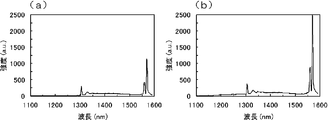
- FIGS. 2 shows a case where the oxygen concentration is about 0.2 ppma
- FIG. 2A shows a nitrogen concentration of 4.9 ⁇ 10 14 atoms / cm 3
- FIG. 2B shows a nitrogen concentration of about 2.2 ⁇ 10 This is the case of 15 atoms / cm 3
- FIG. 2 G-line derived from CiCs (near 1305 nm) and C-line derived from CiOi (near 1570 nm) are observed, but the emission intensity of C-line is as shown in FIGS. 2 (a) and 2 (b). Is clearly different. From this result, it can be seen that the density of CiOi decreases when the nitrogen concentration is low.
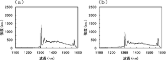
- FIG. 3 shows a case where the oxygen concentration is less than 0.1 ppma
- FIG. 3A shows a nitrogen concentration of 3.6 ⁇ 10 14 atoms / cm 3
- FIG. 3B shows a nitrogen concentration of about 1.7 ⁇ 10 10. This is the case of 15 atoms / cm 3 .
- the G line and the C line are observed as in FIG. 2, but the emission intensity of the G line is clearly different between FIG. 3 (a) and FIG. 3 (b). From this result, it can be seen that the density of CiCs increases when the nitrogen concentration is low.
- TO line near 1130 nm
- derived from silicon is also observed, but since the emission intensity is weak, it cannot be recognized as a peak on the scale of the figure.
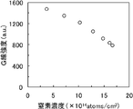
- FIG. 4 shows the relationship between the G-line intensity and the nitrogen concentration
- FIG. 5 shows the relationship between the C-line intensity and the nitrogen concentration. From the results of FIGS. 4 and 5, it can be seen that when the oxygen concentration is less than 0.1 ppma, the C-line intensity decreases regardless of the nitrogen concentration, but the G-line intensity decreases as the nitrogen concentration increases. From this, it can be seen that even if the carbon concentration and the oxygen concentration are substantially the same, when the oxygen concentration is less than 0.1 ppma, the higher the nitrogen concentration, the lower the density of CiCs. Further, for example, when it is desired to increase the density of CiCs while keeping the density of CiOi low, it is understood that the nitrogen concentration may be reduced by setting the oxygen concentration to less than 0.1 ppma.
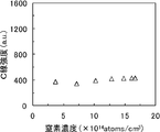
- FIG. 6 shows the relationship between the G-line intensity and the nitrogen concentration
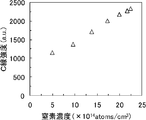
- FIG. 7 shows the relationship between the C-line intensity and the nitrogen concentration in the case of a silicon single crystal substrate having an oxygen concentration of 0.1 to 0.3 ppma. From the results of FIG. 6 and FIG. 7, when the oxygen concentration is 0.1 to 0.3 ppma, the G-ray intensity decreases regardless of the nitrogen concentration, but the C-line intensity increases as the nitrogen concentration increases. Understand. From this, it can be seen that even if the carbon concentration and the oxygen concentration are almost the same, when the oxygen concentration is 0.1 to 0.3 ppma, the higher the nitrogen concentration, the higher the density of CiOi. Further, for example, when it is desired to increase the density of CiOi while keeping the density of CiCs low, it is understood that the nitrogen concentration may be increased by setting the oxygen concentration to 0.1 to 0.3 ppma.
- the relationship between the G-ray intensity and the C-ray intensity and the nitrogen concentration can be obtained by the same method in the photoluminescence method.
- the oxygen concentration of the FZ silicon single crystal substrate differs depending on whether the silicon raw material used for crystal production is polycrystalline silicon or single crystal silicon grown by the CZ method. If the silicon raw material production method is the same, the variation in oxygen concentration is reduced. can do.
- the density of carbon or a complex containing carbon and oxygen can be controlled by adjusting the nitrogen concentration.
- the defect density is controlled by adjusting the nitrogen concentration of the silicon single crystal substrate for controlling the defect density so that the defect density when the electron beam irradiation and the subsequent heat treatment are performed becomes the target value.
- the variation in defect density caused by the silicon single crystal substrate itself can be reduced. Then, by reducing the variation in nitrogen concentration, the variation in defect density can be reduced.
- the reason why the defect density when the electron beam irradiation and the subsequent heat treatment are performed depends on the nitrogen concentration is considered as follows.
- V and substitutional phosphorus Ps react to form VP (V + Ps ⁇ VP).
- V and interstitial oxygen Oi react to form VO (V + Oi ⁇ VO)
- V and VO react to form V 2 O (V + VO ⁇ V 2 O).
- Vs react to form VV (V + V ⁇ VV).
- V and N react to form VN (V + N ⁇ VN). Since the reaction between V and P, O, or N competes with each other, if it is easy to form VN when the nitrogen concentration is high, it may be difficult to form other complexes related to V.
- I and substitutional boron Bs react to form interstitial boron Bi (I + Bs ⁇ Bi), and Bi and Oi react to form BiOi ( Bi + Oi ⁇ BiOi) is known.
- I and substitutional carbon Cs react to form interstitial carbon Ci (I + Cs ⁇ Ci), and Ci and Oi, and Ci and Cs react to form CiOi and CiCs. (Ci + Oi ⁇ CiOi, Ci + Cs ⁇ CiCs).
- I reacts to form an I cluster (I + I +... ⁇ In).
- nitrogen is present at a higher concentration, the reaction between V and N suppresses the recombination of V and I, and as a result, a complex associated with I may be easily formed. .
- the reaction between I and V and light element impurities depends on the absolute concentration and concentration balance of each, so it is extremely complicated. When further heat treatment is performed, the complex disappears or changes in shape. More complicated.
- Example 1 The defect density in the silicon single crystal substrate was controlled by the defect density control method of the present invention as shown in FIG. At this time, it was aimed to control the C-ray intensity to be about 2000 when measured by the cathodoluminescence method as in the experimental example.
- test silicon single crystal substrates having different nitrogen concentrations were irradiated with an electron beam and then heat-treated, and the C-line intensity in the plurality of test silicon single crystal substrates was measured.
- the test silicon single crystal substrate was manufactured from a silicon single crystal grown by the FZ method, and the oxygen concentration was 0.1 to 0.3 ppma.
- the irradiation dose of the electron beam at this time was 1 ⁇ 10 15 / cm 2, and the acceleration voltage of the electron beam was 2 MV.
- the heat treatment temperature was 360 ° C., the time was 45 minutes, and the atmosphere was nitrogen.
- the correlation acquisition step the correlation between the C-line intensity and the nitrogen concentration of the plurality of test silicon single crystal substrates was acquired (FIG. 7).
- the nitrogen concentration of the silicon single crystal substrate prepared in the preparation step was adjusted so that the C-line intensity of the silicon single crystal substrate after the heat treatment step became a target value (about 2000).
- the prepared silicon single crystal substrate was manufactured from a silicon single crystal grown by the FZ method using a silicon single crystal ingot grown by the CZ method as a raw material, and the oxygen concentration was about 0.2 ppma.
- the nitrogen concentration was adjusted to 1.7 ⁇ 10 15 atoms / cm 3 .
- the prepared silicon single crystal substrate was irradiated with an electron beam.
- the electron beam irradiation dose was 1 ⁇ 10 15 / cm 2 and the electron beam acceleration voltage was 2 MV.
- a recovery heat treatment was performed on the silicon single crystal substrate irradiated with the electron beam.
- the temperature of the recovery heat treatment was 360 ° C., the atmosphere was nitrogen, and the time was 45 minutes.
- Example 1 it was confirmed that the defect density of the target value could be obtained by adjusting the nitrogen concentration of the silicon single crystal substrate.
- Example 1 A test silicon single crystal substrate was used, the correlation between the defect density and the nitrogen concentration was not obtained, and the nitrogen concentration of the silicon single crystal substrate to be prepared was not adjusted based on the above correlation. 1 was used to control the defect density of the silicon single crystal substrate. At this time, the FZ silicon single crystal substrate having a nitrogen concentration of 1.0 ⁇ 10 15 atoms / cm 3 and an oxygen concentration of less than 0.1 ppma was irradiated with an electron beam and then subjected to a recovery heat treatment.
- Example 2 The defect density in the silicon single crystal substrate was controlled by the defect density control method of the present invention as shown in FIG. At this time, it was aimed to control the G-ray intensity to be about 1200 when measured by the cathodoluminescence method as in the experimental example.
- test silicon single crystal substrates having different nitrogen concentrations were irradiated with an electron beam and then heat-treated, and the G-ray intensity in the plurality of test silicon single crystal substrates was measured.
- the test silicon single crystal substrate was manufactured from a silicon single crystal grown by the FZ method using a polycrystalline silicon ingot as a raw material, and the oxygen concentration was less than 0.1 ppma.
- the irradiation dose of the electron beam at this time was 1 ⁇ 10 15 / cm 2, and the acceleration voltage of the electron beam was 2 MV.
- the heat treatment temperature was 360 ° C., the time was 45 minutes, and the atmosphere was nitrogen.
- the correlation acquisition step the correlation between the G-ray intensity and the nitrogen concentration of the plurality of test silicon single crystal substrates was acquired (FIG. 4).
- the nitrogen concentration of the silicon single crystal substrate prepared in the preparation step was adjusted so that the G-ray intensity of the silicon single crystal substrate after the heat treatment step became a target value (about 1200).
- the prepared silicon single crystal substrate was manufactured from a silicon single crystal grown by FZ method using a polycrystalline silicon ingot as a raw material, the oxygen concentration was less than 0.1 ppma, and the nitrogen concentration was 1. It was adjusted to 0 ⁇ 10 15 atoms / cm 3 .
- the prepared silicon single crystal substrate was irradiated with an electron beam.
- the electron beam irradiation dose was 1 ⁇ 10 15 / cm 2 and the electron beam acceleration voltage was 2 MV.
- a recovery heat treatment was performed on the silicon single crystal substrate irradiated with the electron beam.
- the temperature of the recovery heat treatment was 360 ° C., the atmosphere was nitrogen, and the time was 45 minutes.
- the C-line intensity of the silicon single crystal substrate was 1225.
- Example 2 it was confirmed that the target value of the defect density could be obtained by adjusting the nitrogen concentration of the silicon single crystal substrate.
- Example 2 A test silicon single crystal substrate was used, the correlation between the defect density and the nitrogen concentration was not obtained, and the nitrogen concentration of the silicon single crystal substrate to be prepared was not adjusted based on the above correlation. 2 was used to control the defect density of the silicon single crystal substrate. At this time, the nitrogen concentration was 1.7 ⁇ 10 15 atoms / cm 3 and the oxygen concentration was less than 0.1 ppma. The FZ silicon single crystal substrate was irradiated with an electron beam and then subjected to a recovery heat treatment.
- the present invention is not limited to the above embodiment.
- the above-described embodiment is an exemplification, and the present invention has any configuration that has substantially the same configuration as the technical idea described in the claims of the present invention and that exhibits the same effects. Are included in the technical scope.
Landscapes
- Engineering & Computer Science (AREA)
- Chemical & Material Sciences (AREA)
- Manufacturing & Machinery (AREA)
- Computer Hardware Design (AREA)
- Physics & Mathematics (AREA)
- Power Engineering (AREA)
- Microelectronics & Electronic Packaging (AREA)
- Metallurgy (AREA)
- Organic Chemistry (AREA)
- Materials Engineering (AREA)
- Crystallography & Structural Chemistry (AREA)
- High Energy & Nuclear Physics (AREA)
- Health & Medical Sciences (AREA)
- Toxicology (AREA)
- Condensed Matter Physics & Semiconductors (AREA)
- General Physics & Mathematics (AREA)
- Crystals, And After-Treatments Of Crystals (AREA)
- Testing Or Measuring Of Semiconductors Or The Like (AREA)
Abstract
La présente invention concerne un procédé de régulation de la densité de défauts dans un substrat monocristallin de silicium, le procédé comprenant une étape de préparation pour préparer un substrat monocristallin de silicium, une étape d'irradiation par un faisceau de particules et une étape de traitement thermique suivant l'étape d'irradiation par un faisceau de particules et le procédé étant caractérisé en ce qu'il comprend une étape de mesure pour, avant l'étape de préparation, irradier un faisceau de particules sur un substrat monocristallin de silicium de test, puis réaliser un traitement thermique et mesurer la densité de défauts générés, et une étape d'acquisition de corrélation pour acquérir la corrélation entre la densité de défauts mesurée et la concentration en azote, la concentration en azote du substrat monocristallin de silicium à préparer étant ajustée sur la base de la corrélation acquise de telle sorte que la densité de défauts dans le substrat monocristallin de silicium après l'étape de traitement thermique atteint une valeur cible. L'invention concerne également un procédé de régulation de la densité de défauts dans un substrat monocristallin de silicium, le procédé permettant de réduire la variation de densité de défauts résultant du substrat monocristallin de silicium et de réguler la densité de défauts avec une précision élevée pendant une étape de fabrication de dispositif pour réguler la densité de défauts par irradiation par un faisceau de particules et traitement thermique.
Priority Applications (3)
| Application Number | Priority Date | Filing Date | Title |
|---|---|---|---|
| DK19820517.1T DK3808879T3 (da) | 2018-06-12 | 2019-05-13 | Fremgangsmåde til kontrol af defektdensitet i et monokrystallinsk siliciumsubstrat |
| EP19820517.1A EP3808879B1 (fr) | 2018-06-12 | 2019-05-13 | Procédé de régulation de densité de défauts dans un substrat monocristallin de silicium |
| CN201980039589.7A CN112334608B (zh) | 2018-06-12 | 2019-05-13 | 单晶硅基板中的缺陷密度的控制方法 |
Applications Claiming Priority (2)
| Application Number | Priority Date | Filing Date | Title |
|---|---|---|---|
| JP2018112062A JP7006517B2 (ja) | 2018-06-12 | 2018-06-12 | シリコン単結晶基板中の欠陥密度の制御方法 |
| JP2018-112062 | 2018-06-12 |
Publications (1)
| Publication Number | Publication Date |
|---|---|
| WO2019239762A1 true WO2019239762A1 (fr) | 2019-12-19 |
Family
ID=68842170
Family Applications (1)
| Application Number | Title | Priority Date | Filing Date |
|---|---|---|---|
| PCT/JP2019/019004 WO2019239762A1 (fr) | 2018-06-12 | 2019-05-13 | Procédé de régulation de densité de défauts dans un substrat monocristallin de silicium |
Country Status (6)
| Country | Link |
|---|---|
| EP (1) | EP3808879B1 (fr) |
| JP (1) | JP7006517B2 (fr) |
| CN (1) | CN112334608B (fr) |
| DK (1) | DK3808879T3 (fr) |
| TW (1) | TWI801586B (fr) |
| WO (1) | WO2019239762A1 (fr) |
Cited By (2)
| Publication number | Priority date | Publication date | Assignee | Title |
|---|---|---|---|---|
| JPWO2021186944A1 (fr) * | 2020-03-17 | 2021-09-23 | ||
| WO2021199687A1 (fr) * | 2020-04-02 | 2021-10-07 | 信越半導体株式会社 | Procédé de régulation de concentration de donneur dans substrat monocristallin de silicium |
Citations (9)
| Publication number | Priority date | Publication date | Assignee | Title |
|---|---|---|---|---|
| JPH11135509A (ja) | 1997-10-29 | 1999-05-21 | Sanken Electric Co Ltd | 半導体装置の製造方法 |
| JP2000200792A (ja) | 1998-11-05 | 2000-07-18 | Denso Corp | 半導体装置の製造方法 |
| JP2001068477A (ja) * | 1999-08-27 | 2001-03-16 | Komatsu Electronic Metals Co Ltd | エピタキシャルシリコンウエハ |
| JP2001240490A (ja) * | 2000-02-25 | 2001-09-04 | Sumitomo Metal Ind Ltd | 半導体シリコンウエーハの製造方法 |
| JP2004304095A (ja) * | 2003-04-01 | 2004-10-28 | Sumitomo Mitsubishi Silicon Corp | シリコンウェーハおよびその製造方法 |
| WO2007055352A1 (fr) | 2005-11-14 | 2007-05-18 | Fuji Electric Device Technology Co., Ltd. | Dispositif a semi-conducteur et procede de fabrication associe |
| WO2013100155A1 (fr) | 2011-12-28 | 2013-07-04 | 富士電機株式会社 | Dispositif semi-conducteur et procédé de production du dispositif semi-conducteur |
| JP2015023062A (ja) * | 2013-07-16 | 2015-02-02 | 信越半導体株式会社 | 拡散ウェーハの製造方法 |
| JP2015156420A (ja) * | 2014-02-20 | 2015-08-27 | 信越半導体株式会社 | シリコン単結晶中の炭素濃度評価方法及び半導体デバイスの製造方法 |
Family Cites Families (5)
| Publication number | Priority date | Publication date | Assignee | Title |
|---|---|---|---|---|
| JP2001067477A (ja) * | 1999-08-27 | 2001-03-16 | Matsushita Electric Ind Co Ltd | 個人識別システム |
| JP2006054350A (ja) * | 2004-08-12 | 2006-02-23 | Komatsu Electronic Metals Co Ltd | 窒素ドープシリコンウェーハとその製造方法 |
| JP6036670B2 (ja) * | 2013-12-10 | 2016-11-30 | 信越半導体株式会社 | シリコン単結晶基板の欠陥濃度評価方法 |
| JP6083412B2 (ja) * | 2014-04-01 | 2017-02-22 | 信越半導体株式会社 | 再結合ライフタイムの制御方法及びシリコン基板の製造方法 |
| JP6447351B2 (ja) * | 2015-05-08 | 2019-01-09 | 株式会社Sumco | シリコンエピタキシャルウェーハの製造方法およびシリコンエピタキシャルウェーハ |
-
2018
- 2018-06-12 JP JP2018112062A patent/JP7006517B2/ja active Active
-
2019
- 2019-05-13 CN CN201980039589.7A patent/CN112334608B/zh active Active
- 2019-05-13 DK DK19820517.1T patent/DK3808879T3/da active
- 2019-05-13 WO PCT/JP2019/019004 patent/WO2019239762A1/fr unknown
- 2019-05-13 EP EP19820517.1A patent/EP3808879B1/fr active Active
- 2019-05-21 TW TW108117522A patent/TWI801586B/zh active
Patent Citations (9)
| Publication number | Priority date | Publication date | Assignee | Title |
|---|---|---|---|---|
| JPH11135509A (ja) | 1997-10-29 | 1999-05-21 | Sanken Electric Co Ltd | 半導体装置の製造方法 |
| JP2000200792A (ja) | 1998-11-05 | 2000-07-18 | Denso Corp | 半導体装置の製造方法 |
| JP2001068477A (ja) * | 1999-08-27 | 2001-03-16 | Komatsu Electronic Metals Co Ltd | エピタキシャルシリコンウエハ |
| JP2001240490A (ja) * | 2000-02-25 | 2001-09-04 | Sumitomo Metal Ind Ltd | 半導体シリコンウエーハの製造方法 |
| JP2004304095A (ja) * | 2003-04-01 | 2004-10-28 | Sumitomo Mitsubishi Silicon Corp | シリコンウェーハおよびその製造方法 |
| WO2007055352A1 (fr) | 2005-11-14 | 2007-05-18 | Fuji Electric Device Technology Co., Ltd. | Dispositif a semi-conducteur et procede de fabrication associe |
| WO2013100155A1 (fr) | 2011-12-28 | 2013-07-04 | 富士電機株式会社 | Dispositif semi-conducteur et procédé de production du dispositif semi-conducteur |
| JP2015023062A (ja) * | 2013-07-16 | 2015-02-02 | 信越半導体株式会社 | 拡散ウェーハの製造方法 |
| JP2015156420A (ja) * | 2014-02-20 | 2015-08-27 | 信越半導体株式会社 | シリコン単結晶中の炭素濃度評価方法及び半導体デバイスの製造方法 |
Non-Patent Citations (5)
| Title |
|---|
| K. TAKANO ET AL., PROCEEDING OF THE 27TH INTERNATIONAL SYMPOSIUM ON POWER SEMICONDUCTOR DEVICES & IC'S, 2015, pages 129 |
| KIYOI ET AL.: "The 61st Japan Society of Applied Physics Spring Meeting", MEETING PROCEEDINGS, vol. 19, pages 9 - 14 |
| See also references of EP3808879A4 |
| SGOUROU, E. N. ET AL.: "Infrared study of defects in nitrogen- doped electron irradiated silicon", J. MATER. SCI, MATER. ELECTRON., vol. 27, no. 2, 4 November 2015 (2015-11-04), pages 2054 - 2061, XP035915176, ISSN: 0957-4522, DOI: 10.1007/s10854-015-3991-2 * |
| SUGIYAMA ET AL., THE 4TH WORKSHOP ON POWER DEVICE SILICON AND RELATED SEMICONDUCTOR MATERIALS, pages 71 |
Cited By (8)
| Publication number | Priority date | Publication date | Assignee | Title |
|---|---|---|---|---|
| JPWO2021186944A1 (fr) * | 2020-03-17 | 2021-09-23 | ||
| WO2021186944A1 (fr) * | 2020-03-17 | 2021-09-23 | 信越半導体株式会社 | Procédé de contrôle de la concentration de donneurs dans un substrat monocristallin de silicium |
| JP7334849B2 (ja) | 2020-03-17 | 2023-08-29 | 信越半導体株式会社 | シリコン単結晶基板中のドナー濃度の制御方法 |
| EP4123686A4 (fr) * | 2020-03-17 | 2024-05-01 | Shinetsu Handotai Kk | Procédé de contrôle de la concentration de donneurs dans un substrat monocristallin de silicium |
| WO2021199687A1 (fr) * | 2020-04-02 | 2021-10-07 | 信越半導体株式会社 | Procédé de régulation de concentration de donneur dans substrat monocristallin de silicium |
| JP2021163929A (ja) * | 2020-04-02 | 2021-10-11 | 信越半導体株式会社 | シリコン単結晶基板中のドナー濃度の制御方法 |
| JP7264100B2 (ja) | 2020-04-02 | 2023-04-25 | 信越半導体株式会社 | シリコン単結晶基板中のドナー濃度の制御方法 |
| EP4131341A4 (fr) * | 2020-04-02 | 2024-05-01 | Shinetsu Handotai Kk | Procédé de régulation de concentration de donneur dans substrat monocristallin de silicium |
Also Published As
| Publication number | Publication date |
|---|---|
| TWI801586B (zh) | 2023-05-11 |
| CN112334608A (zh) | 2021-02-05 |
| JP7006517B2 (ja) | 2022-01-24 |
| DK3808879T3 (da) | 2023-05-01 |
| EP3808879B1 (fr) | 2023-03-01 |
| TW202002116A (zh) | 2020-01-01 |
| EP3808879A1 (fr) | 2021-04-21 |
| EP3808879A4 (fr) | 2022-03-02 |
| CN112334608B (zh) | 2022-07-26 |
| JP2019214488A (ja) | 2019-12-19 |
Similar Documents
| Publication | Publication Date | Title |
|---|---|---|
| JP6083412B2 (ja) | 再結合ライフタイムの制御方法及びシリコン基板の製造方法 | |
| JP6268039B2 (ja) | 検量線の作成方法、不純物濃度の測定方法、及び半導体ウェハの製造方法 | |
| JP6292131B2 (ja) | シリコン基板の選別方法 | |
| WO2015087485A1 (fr) | Procédé d'évaluation de densité de défauts pour substrat en silicium monocristallin | |
| KR20140111973A (ko) | 포화 전압 추정 방법 및 실리콘 에피택셜 웨이퍼의 제조 방법 | |
| JP2015111615A (ja) | シリコン単結晶中の炭素濃度評価方法、及び、半導体デバイスの製造方法 | |
| WO2019239762A1 (fr) | Procédé de régulation de densité de défauts dans un substrat monocristallin de silicium | |
| Oliviero et al. | Helium implantation defects in SiC: A thermal helium desorption spectrometry investigation | |
| Nakamura et al. | Size and dopant-concentration dependence of photoluminescence properties of ion-implanted phosphorus-and boron-codoped Si nanocrystals | |
| JP6881292B2 (ja) | 再結合ライフタイムの制御方法 | |
| JP6777046B2 (ja) | 再結合ライフタイムの制御方法 | |
| Sobolev et al. | Luminescent and Structural Properties of Electron-Irradiated Silicon Light-Emitting Diodes with Dislocation-Related Luminescence | |
| Inoue et al. | Infrared defect dynamics–radiation induced complexes in silicon crystals grown by various techniques | |
| JP7259791B2 (ja) | シリコンウェーハへのクラスターイオン注入による白傷欠陥低減効果の評価方法及びエピタキシャルシリコンウェーハの製造方法 | |
| WO2021199687A1 (fr) | Procédé de régulation de concentration de donneur dans substrat monocristallin de silicium | |
| JP7103314B2 (ja) | シリコン単結晶基板中の炭素濃度評価方法 | |
| JP7334849B2 (ja) | シリコン単結晶基板中のドナー濃度の制御方法 | |
| Yamagata et al. | Micro-Photoluminescence study on the influence of oxidation on stacking faults in 4H-SiC epilayers | |
| JP6766786B2 (ja) | シリコン単結晶基板中の炭素濃度評価方法、及び半導体デバイスの製造方法 | |
| Sobolev et al. | Electroluminescent properties of strained p-Si LEDs | |
| CN111801782A (zh) | 碳浓度评价方法 | |
| Bykovsky et al. | Influence of fast neutrons on the recombination and electrical properties of neutron transmutation doped gallium arsenide |
Legal Events
| Date | Code | Title | Description |
|---|---|---|---|
| 121 | Ep: the epo has been informed by wipo that ep was designated in this application |
Ref document number: 19820517 Country of ref document: EP Kind code of ref document: A1 |
|
| NENP | Non-entry into the national phase |
Ref country code: DE |
|
| ENP | Entry into the national phase |
Ref document number: 2019820517 Country of ref document: EP Effective date: 20210112 |