WO2019235560A1 - フィラー含有フィルム - Google Patents
フィラー含有フィルム Download PDFInfo
- Publication number
- WO2019235560A1 WO2019235560A1 PCT/JP2019/022492 JP2019022492W WO2019235560A1 WO 2019235560 A1 WO2019235560 A1 WO 2019235560A1 JP 2019022492 W JP2019022492 W JP 2019022492W WO 2019235560 A1 WO2019235560 A1 WO 2019235560A1
- Authority
- WO
- WIPO (PCT)
- Prior art keywords
- filler
- resin layer
- insulating resin
- containing film
- film
- Prior art date
Links
Images


Classifications
-
- C—CHEMISTRY; METALLURGY
- C09—DYES; PAINTS; POLISHES; NATURAL RESINS; ADHESIVES; COMPOSITIONS NOT OTHERWISE PROVIDED FOR; APPLICATIONS OF MATERIALS NOT OTHERWISE PROVIDED FOR
- C09J—ADHESIVES; NON-MECHANICAL ASPECTS OF ADHESIVE PROCESSES IN GENERAL; ADHESIVE PROCESSES NOT PROVIDED FOR ELSEWHERE; USE OF MATERIALS AS ADHESIVES
- C09J11/00—Features of adhesives not provided for in group C09J9/00, e.g. additives
- C09J11/02—Non-macromolecular additives
- C09J11/04—Non-macromolecular additives inorganic
-
- C—CHEMISTRY; METALLURGY
- C09—DYES; PAINTS; POLISHES; NATURAL RESINS; ADHESIVES; COMPOSITIONS NOT OTHERWISE PROVIDED FOR; APPLICATIONS OF MATERIALS NOT OTHERWISE PROVIDED FOR
- C09J—ADHESIVES; NON-MECHANICAL ASPECTS OF ADHESIVE PROCESSES IN GENERAL; ADHESIVE PROCESSES NOT PROVIDED FOR ELSEWHERE; USE OF MATERIALS AS ADHESIVES
- C09J201/00—Adhesives based on unspecified macromolecular compounds
-
- C—CHEMISTRY; METALLURGY
- C09—DYES; PAINTS; POLISHES; NATURAL RESINS; ADHESIVES; COMPOSITIONS NOT OTHERWISE PROVIDED FOR; APPLICATIONS OF MATERIALS NOT OTHERWISE PROVIDED FOR
- C09J—ADHESIVES; NON-MECHANICAL ASPECTS OF ADHESIVE PROCESSES IN GENERAL; ADHESIVE PROCESSES NOT PROVIDED FOR ELSEWHERE; USE OF MATERIALS AS ADHESIVES
- C09J7/00—Adhesives in the form of films or foils
- C09J7/10—Adhesives in the form of films or foils without carriers
-
- C—CHEMISTRY; METALLURGY
- C09—DYES; PAINTS; POLISHES; NATURAL RESINS; ADHESIVES; COMPOSITIONS NOT OTHERWISE PROVIDED FOR; APPLICATIONS OF MATERIALS NOT OTHERWISE PROVIDED FOR
- C09J—ADHESIVES; NON-MECHANICAL ASPECTS OF ADHESIVE PROCESSES IN GENERAL; ADHESIVE PROCESSES NOT PROVIDED FOR ELSEWHERE; USE OF MATERIALS AS ADHESIVES
- C09J7/00—Adhesives in the form of films or foils
- C09J7/30—Adhesives in the form of films or foils characterised by the adhesive composition
- C09J7/35—Heat-activated
-
- H—ELECTRICITY
- H01—ELECTRIC ELEMENTS
- H01R—ELECTRICALLY-CONDUCTIVE CONNECTIONS; STRUCTURAL ASSOCIATIONS OF A PLURALITY OF MUTUALLY-INSULATED ELECTRICAL CONNECTING ELEMENTS; COUPLING DEVICES; CURRENT COLLECTORS
- H01R11/00—Individual connecting elements providing two or more spaced connecting locations for conductive members which are, or may be, thereby interconnected, e.g. end pieces for wires or cables supported by the wire or cable and having means for facilitating electrical connection to some other wire, terminal, or conductive member, blocks of binding posts
- H01R11/01—Individual connecting elements providing two or more spaced connecting locations for conductive members which are, or may be, thereby interconnected, e.g. end pieces for wires or cables supported by the wire or cable and having means for facilitating electrical connection to some other wire, terminal, or conductive member, blocks of binding posts characterised by the form or arrangement of the conductive interconnection between the connecting locations
-
- H—ELECTRICITY
- H01—ELECTRIC ELEMENTS
- H01R—ELECTRICALLY-CONDUCTIVE CONNECTIONS; STRUCTURAL ASSOCIATIONS OF A PLURALITY OF MUTUALLY-INSULATED ELECTRICAL CONNECTING ELEMENTS; COUPLING DEVICES; CURRENT COLLECTORS
- H01R43/00—Apparatus or processes specially adapted for manufacturing, assembling, maintaining, or repairing of line connectors or current collectors or for joining electric conductors
Definitions
- the present invention relates to a filler-containing film.
- Filler-containing films in which filler is dispersed in the resin layer are used in a wide variety of applications such as matte films, condenser films, optical films, label films, anti-static films, conductive films, and anisotropic conductive films.
- Patent Literature 1 Patent Literature 2, Patent Literature 3, Patent Literature 4
- the resin forming the filler-containing film is prevented from flowing unnecessarily during thermocompression bonding, and the uneven distribution of the filler is suppressed by optical characteristics, mechanical properties. It is desirable in terms of characteristics or electrical characteristics.
- the conductive resin particles in the insulating resin layer can be used for high-density mounting of electronic components. If the resin is dispersed at a high density, the conductive particles move unnecessarily due to the resin flow at the time of mounting the electronic component and are unevenly distributed between the terminals, causing a short circuit. Therefore, it is desirable to suppress such resin flow. .
- the insulating resin layer is made to contain fine solids such as a melt viscosity modifier and a thixotropic agent (Patent Documents 5 and 6).
- JP 2006-15680 A JP2015-138904A JP2013-103368A JP 2014-183266 A Japanese Patent No. 6187665 Japanese Unexamined Patent Publication No. 2016-031888
- An insulating resin layer containing a fine solid is generally formed by coating and drying an insulating resin layer forming composition in which a fine solid is dispersed.
- an insulating resin layer containing a minute solid in a high concentration by applying and drying the insulating resin layer forming composition
- the dry surface of the insulating resin layer that is, the insulating resin layer forming composition
- the surface of the solvent contained in the composition evaporates), because the roughness derived from the fine solids is formed.
- Temporary pressure bonding at the time is not performed uniformly, and the sticking state becomes unstable.
- thermocompression during the main pressure bonding is not performed uniformly, resulting in disordered arrangement of the conductive particles regularly arranged in the insulating resin layer, improving the trapping property of the conductive particles at the terminals of the electronic component, and short-circuiting.
- the suppression will be adversely affected. This problem is particularly noticeable when the electronic component is small and the terminal size is narrowed.
- the problem of the adhesiveness fall of the filler containing film surface may become remarkable when it thins, compared with the case where it is thick.
- an object of the present invention is to suppress the disorder of the filler arrangement when the filler-containing film is thermocompression bonded to an article.
- the present inventor forms a filler-containing film in which a filler such as conductive particles and a fine solid having a different forming material from the filler are held in an insulating resin layer, and forms an insulating resin layer containing the fine solid. So that the dry surface of the insulating resin layer does not appear on the surface of the filler-containing film when manufacturing by the step of forming the insulating resin layer by coating the composition for use and the step of pressing the filler into the insulating resin layer Then, it discovered that disorder of the arrangement
- the present invention is a filler-containing film in which a filler, a fine solid different from a filler and a forming material are held in an insulating resin layer, and the filler repeats a predetermined arrangement in a plan view,
- a filler-containing film in which the ratio of the repeating pitch of the filler after thermocompression bonding with respect to before thermocompression bonding is within 300%, in particular,
- the insulating resin layer is formed from a laminate of two insulating resin layers, and a low-viscosity resin layer having a minimum melt viscosity in the range of 30 to 200 ° C. lower than that of the insulating resin layer is the insulating resin layer
- stacked is provided.
- this invention apply
- Forming a process A process of pushing the filler from the surface of the insulating resin layer opposite to the peeling substrate, A step of laminating an insulating resin layer into which a filler is pressed, and an insulating resin layer separate from the insulating resin layer, with the release substrate as the outside;
- Providing a method for producing a filler-containing film having As a second production method a step of applying an insulating resin layer forming composition containing a minute solid on a release substrate, and forming an insulating resin layer on the release substrate, A step of forming a laminate of insulating resin layers by laminating two insulating resin layers with their release substrates facing outside, A step of pushing a filler into the laminate of the insulating resin layer, Providing a
- the surface of the filler-containing film is roughened even though a fine solid is contained in the insulating resin layer in an appropriate blending amount in terms of viscosity adjustment and the like. Because it is not formed, the film surface has good adhesion to various articles. Therefore, the filler of the filler-containing film attached to the article by thermocompression bonding can substantially maintain the predetermined arrangement before thermocompression bonding.
- the filler of the filler-containing film of the present invention is conductive particles
- the filler-containing film of the present invention is used for anisotropic conductive connection between electronic parts, temporary pressing can be performed well, However, since the arrangement of the conductive particles is hardly disturbed, the predetermined arrangement before the thermocompression bonding can be substantially maintained. Therefore, even when the electronic components are small and the terminal size is narrowed, the electronic components can be favorably anisotropically connected to each other.
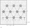
- FIG. 1A is a plan view showing a filler arrangement of a filler-containing film 1A of an example.
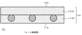
- FIG. 1B is a cross-sectional view of the filler-containing film 1A of the example.
- Drawing 2A is an explanatory view of the manufacturing method of filler content film 1A of an example.
- Drawing 2B is an explanatory view of the manufacturing method of filler content film 1A of an example.
- Drawing 2C is an explanatory view of the manufacturing method of filler content film 1A of an example.
- Drawing 2D is an explanatory view of the manufacturing method of filler content film 1A of an example.
- FIG. 2E is an explanatory diagram of a method for producing the filler-containing film 1A of the example.
- FIG. 1A is a plan view showing a filler arrangement of a filler-containing film 1A of an example.
- FIG. 1B is a cross-sectional view of the filler-containing film 1A of the example.
- Drawing 2A is
- FIG. 2F is an explanatory diagram of a method for producing the filler-containing film 1A of the example.
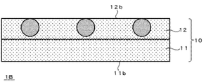
- FIG. 3 is a cross-sectional view of the filler-containing film 1B of the example.
- Drawing 4A is an explanatory view of the manufacturing method of filler content film 1B of an example.
- Drawing 4B is an explanatory view of the manufacturing method of filler content film 1B of an example.
- Drawing 4C is an explanatory view of the manufacturing method of filler content film 1B of an example.
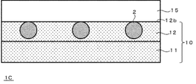
- FIG. 5 is a cross-sectional view of the filler-containing film 1C of the example.
- Drawing 6 is an explanatory view of the manufacturing method of filler content film 1C of an example.
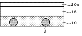
- FIG. 7 is a cross-sectional view of the filler-containing film 1D of the example.
- Drawing 8A is an explanatory view of the manufacturing method of filler content film 1D of an example.
- Drawing 8B is an explanatory view of the manufacturing method of filler content film 1D of an example.
- Drawing 8C is an explanatory view of the manufacturing method of filler content film 1D of an example.
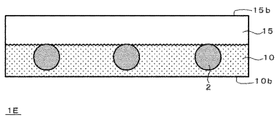
- FIG. 9 is a cross-sectional view of the filler-containing film 1E of the example.
- FIG. 10A is an explanatory diagram of a method for producing the filler-containing film 1E of the example.
- Drawing 10B is an explanatory view of the manufacturing method of filler content film 1E of an example.
- FIG. 10C is an explanatory diagram of a method for producing the filler-containing film 1E of the example.
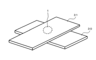
- FIG. 11 is a perspective view of a sample for an adhesive strength test.
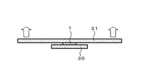
- FIG. 12 is an explanatory diagram of an adhesive strength test method.
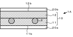
- FIG. 1A is a plan view showing the filler arrangement of the filler-containing film 1A of the example, and FIG. 1B is an XX cross-sectional view thereof.
- This filler-containing film 1A contains conductive particles as the filler 2 and is used as an anisotropic conductive film. The conductive particles are held in the insulating resin layer 10 in a regular arrangement in which a predetermined arrangement is repeated. .
- the insulating resin layer 10 contains a fine solid 3 in addition to the filler 2.
- the regular filler arrangement before thermocompression spreads after thermocompression, and the repeated pitch of the array becomes wider than before thermocompression-bonding.
- the variation in the repeat pitch also increases, and the filler arrangement is disturbed.
- the filler movement amount and the array are less disturbed, and the filler repeat pitch after the thermocompression before the thermocompression is reduced.
- the ratio is within 300%, preferably within 250%, more preferably within 200%.
- the relative positional relationship of the filler arrangement is maintained before and after thermocompression, so that the distance between the centers of the nearest fillers before thermocompression is the closest after thermocompression.
- the distance between the centers of the fillers can be within 3 times, within 2.5 times, and within 2 times.
- the filler-containing film of the present invention has a thermocompression bonding condition in which the ratio of repeated pitches before and after thermocompression bonding is equal to or less than the above numerical value. This is because, according to the method for producing a filler-containing film of the present invention, since the surface of the filler-containing film 1A becomes a release surface from the release substrate, the insulating resin layer 10 contains a large amount of fine solids 3. However, the surface of the filler-containing film 1A does not become rough and becomes a smooth surface. When the smooth surface is attached to an article and heated and pressurized, the filler-containing film is uniformly pressed and regularly arranged in the film.
- the solid solids do not interfere with the pressing force being applied uniformly to the filler, and the filler arrangement is prevented from being disturbed unevenly, and the filler arrangement after heating and pressurization has expanded the original arrangement uniformly. This is considered to be because the portion where the ratio of the filler repeat pitch before and after thermocompression bonding is locally increased is reduced.
- thermocompression bonding is not performed on a smooth surface, nonuniformity occurs in the amount of filler movement and disorder of the thermocompression bonding. Therefore, when the filler-containing film is configured as an anisotropic conductive film, if the fine pitch bump array is thermocompression bonded with the anisotropic conductive film, the disorder of the filler array may be relatively large.
- the filler 2 depending on the use of the filler-containing film, known inorganic fillers (metal particles, metal oxide particles, metal nitride particles, etc.), organic fillers (resin particles, rubber particles, etc.), Filler in which organic and inorganic materials are mixed (for example, particles whose core is formed of a resin material and metal-plated on the surface (metal-coated resin particles), and in which insulating fine particles are attached to the surface of conductive particles The surface of the conductive particles is subjected to insulation treatment, etc.) according to the performance required for applications such as hardness and optical performance.
- inorganic fillers metal particles, metal oxide particles, metal nitride particles, etc.
- organic fillers resin particles, rubber particles, etc.
- Filler in which organic and inorganic materials are mixed for example, particles whose core is formed of a resin material and metal-plated on the surface (metal-coated resin particles), and in which insulating fine particles are attached to the surface of conductive particles
- a silica filler for example, in an optical film or a matte film, a silica filler, a titanium oxide filler, a styrene filler, an acrylic filler, a melamine filler, various titanates, and the like can be used.
- titanium oxide, magnesium titanate, zinc titanate, bismuth titanate, lanthanum oxide, calcium titanate, strontium titanate, barium titanate, barium zirconate titanate, lead zirconate titanate and mixtures thereof Etc. can be used.
- the adhesive film can contain polymer rubber particles, silicone rubber particles, and the like. In the conductive film and the anisotropic conductive film, conductive particles are contained.
- the conductive particles include metal particles such as nickel, cobalt, silver, copper, gold, and palladium, alloy particles such as solder, metal-coated resin particles, and metal-coated resin particles having insulating fine particles attached to the surface. . Two or more kinds can be used in combination. Among these, the metal-coated resin particles are preferable in that the resin particles repel after being connected, so that the contact with the terminal is easily maintained and the conduction performance is stabilized. In addition, the surface of the conductive particles may be subjected to an insulation treatment that does not hinder the conduction characteristics by a known technique.
- the particle diameter of the filler 2 can be determined according to the use of the filler-containing film.
- the particle diameter of the filler 2 in order to improve the indentation precision of the filler at the time of manufacture of a filler containing film, Preferably it is 1 micrometer or more, More preferably, it is 2.5 micrometers or more.
- the particle diameter in order to suppress the influence of the position shift of the filler at the time of manufacture of a filler containing film, Preferably it is 200 micrometers or less, More preferably, it is 50 micrometers or less.
- the particle diameter means an average particle diameter.
- the average particle diameter of the filler in the filler-containing film can be determined from a planar image or a cross-sectional image.
- the average particle size of the filler as raw material particles before being contained in the filler-containing film can be determined using a wet flow type particle size / shape analyzer FPIA-3000 (Malvern). When fine particles such as insulating fine particles are attached to the filler, the diameter not including the fine particles is defined as the particle size.
- CV value standard deviation / average
- the filler-containing film is easily pressed evenly when the filler-containing film is pressed onto the article, and the pressing force can be prevented from being concentrated locally. Therefore, when the filler-containing film is configured as an anisotropic conductive film, the stability of the connection is improved, and after the connection, the connection state can be accurately evaluated by observing the indentation or the sandwiched state of the filler. .
- the terminal size is relatively large (FOB etc.) or relatively small (COG etc.) It is possible to accurately confirm the connection state by observing the indentation and the state of sandwiching the conductive particles. Therefore, inspection after anisotropic connection becomes easy, and it can be expected to improve the productivity of the connection process.
- the filler has a regular arrangement in which a predetermined arrangement is repeated.
- the arrangement of the filler 2 is a hexagonal lattice arrangement. It has become.
- examples of the regular arrangement of the filler include a lattice arrangement such as a square lattice, a rectangular lattice, and an orthorhombic lattice. A plurality of grids having different shapes may be combined. Particle rows in which fillers are linearly arranged at predetermined intervals may be arranged in parallel at predetermined intervals.
- the region where the fillers are densely arranged and the region where the fillers are sparsely arranged may be regularly repeated.
- the unit which the fillers are contacting may comprise the regular repeating unit of a filler.
- the filler-containing film is an anisotropic conductive film, it is more preferable to arrange the conductive particles in a non-contact regular arrangement in order to achieve both capture stability and short-circuit suppression at the terminal.
- Whether or not the fillers are regularly arranged is, for example, whether or not a predetermined arrangement of the fillers is repeated in the longitudinal direction of the film (winding direction when the filler-containing film is used as a wound body). Can be determined by observing.
- the lattice axis or the arrangement axis of the arrangement may be parallel to or crossing at least one of the longitudinal direction of the filler-containing film and the direction perpendicular to the longitudinal direction, It can be determined according to the article to which the filler-containing film is pressure-bonded.
- the distance between the fillers can be determined according to the article to be connected and the use, and the number density of the fillers is usually 10 pieces / mm 2 or more and 100,000 pieces / mm 2 or less, preferably 30 pieces / mm 2. As described above, it can be appropriately determined within the range of 70000 pieces / mm 2 or less.
- the filler-containing film is an anisotropic conductive film
- the interparticle distance of the conductive particles used as the filler 2 is appropriately determined according to the size, shape, and terminal pitch of the terminals connected by the anisotropic conductive film. Can be determined.
- the number density of the conductive particles may be 30 / mm 2 or more, and preferably 150 to 70000 / mm 2 . Particularly in the case of fine pitch use, it is preferably 6000 to 42000 pieces / mm 2 , more preferably 10,000 to 40000 pieces / mm 2 , and still more preferably 15000 to 35000 pieces / mm 2 .
- the particle diameter of the conductive particles is 10 ⁇ m or more, the number density of the conductive particles is preferably 30 to 6000 / mm 2 .
- the filler area occupancy calculated by the following formula is 0.3% or more from the viewpoint of expressing the filler-containing effect.
- the area occupancy of the filler is 35% or less and more preferably 30% or less from the viewpoint of suppressing the thrust required for the pressing jig to press the filler-containing film to the article.
- Filler area occupancy (%) [number density of filler in plan view] ⁇ [average of plan view area of one filler] ⁇ 100
- the number density of the filler is obtained by observing with a metal microscope, and is also observed with image analysis software (for example, WinROOF (Mitani Corporation), A Image-kun (registered trademark) (Asahi Kasei Engineering Corporation), etc.). May be obtained by measuring.
- image analysis software for example, WinROOF (Mitani Corporation), A Image-kun (registered trademark) (Asahi Kasei Engineering Corporation), etc.
- the observation method and the measurement method are not limited to the above.
- the vertices of the fillers in the film thickness direction are flush with the surface of the insulating resin layer 10 or a plane parallel to the surface. Preferably it is. Thereby, it becomes easy to make the filler-containing film uniformly press-bonded to the article.
- Insulating resin layer 10 can contain various fine solids 3 having different formation materials from filler 2 in order to impart functions different from filler 2 to filler-containing film 1A.
- the fine solid 3 can contain a viscosity modifier, a thixotropic agent, a polymerization initiator, a coupling agent, a flame retardant, and the like. More specifically, examples of the viscosity modifier include silica powder and alumina powder.
- the filler 2 and the fine solid 3 when conductive particles are used as the filler 2 and the filler-containing film is an anisotropic conductive film, the fine solid as described in Patent Document 5 is used.
- the conductive particles are held in the insulating resin layer by kneading into the insulating resin layer and pushing the conductive particles into the insulating resin layer, the conductive particles and the fine solids are both distributed in the insulating resin layer. Can be easily distinguished by the state.
- the particle size of the fine solid 3 is preferably smaller than the particle size of the filler 2.
- the fine solid contained as a viscosity modifier preferably has an average particle size. Can be less than 1 ⁇ m, more preferably 5 nm to 0.3 ⁇ m, or preferably 1/3 to 1/2 of the average particle diameter of the conductive particles contained as filler.
- the fine solids are kneaded into the insulating resin layer and the conductive particles are pushed into the insulating resin layer.
- the anisotropic conductive film is manufactured by this, there is no particular limitation as long as the indentation of the conductive particles is not hindered.
- the fine solid is 3% by mass or more.
- the amount is 5% by mass or more, and the fine solid 3 is formed in the insulating resin layer 10 at a high concentration so that it is necessary to push in anisotropic conductive connection in two stages. It can be included.
- the content of the fine solid 3 is preferably 50% by mass or less, and 40% by mass or less with respect to the insulating resin layer 10 from the viewpoint of securing the fluidity necessary for the film for connecting electronic components. More preferred is 35% by mass or less.
- the insulating resin layer may be comprised from the single insulating resin layer, and may be comprised from the laminated body of the several insulating resin layer.
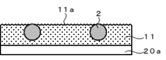
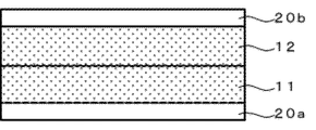
- the insulating resin layer 10 of the filler-containing film 1A shown in FIGS. 1A and 1B is obtained by applying the same insulating resin layer-forming composition onto a smooth release substrate by a method for producing a filler-containing film described later.
- the insulating resin layers 11 and 12 formed by drying are laminated with their dry surfaces on the inside and the surface on the peeling substrate side on the outside. In the filler-containing film 1A, the interface between the two insulating resin layers 11 and 12 can be observed.
- Roughness derived from fine solids contained in the composition is likely to appear on the surface coated with the insulating resin layer-forming composition and dried, but as shown in FIG. 1B, the insulating resin layer 11, When the coating and drying surface in No. 12 is overlapped, the surface of the filler-containing film becomes the surface to which the smooth surface of the release substrate is transferred, so that it is easy to thermocompression-bond the filler-containing film to the article uniformly. It is done.
- the resin composition forming the insulating resin layer 10 is appropriately selected according to the use of the filler-containing film, and can be formed from a thermoplastic resin composition, a high-viscosity adhesive resin composition, and a curable resin composition.
- the filler-containing film is an anisotropic conductive film, it is formed from a polymerizable compound and a polymerization initiator in the same manner as the resin composition forming the insulating resin layer of the anisotropic conductive film described in Patent Document 5.
- the curable resin composition to be used can be used.
- a thermal polymerization initiator may be used, a photopolymerization initiator may be used, or they may be used in combination.
- a cationic polymerization initiator is used as the thermal polymerization initiator
- an epoxy resin is used as the thermopolymerizable compound
- a radical photopolymerization initiator is used as the photopolymerization initiator
- an acrylate compound is used as the photopolymerizable compound.
- a thermal anionic polymerization initiator may be used as the thermal polymerization initiator.
- the thermal anionic polymerization initiator it is preferable to use a microcapsule-type latent curing agent formed by coating an imidazole-modified product as a nucleus and the surface thereof with polyurethane.
- the minimum melt viscosity of the insulating resin layer 10 is not particularly limited as long as the filler is pushed into the insulating resin layer, but in order to suppress unnecessary flow of the filler 2 when the filler-containing film 1A is thermocompression bonded to an article, It is preferably 1500 Pa ⁇ s or more, more preferably 2000 Pa ⁇ s or more, further preferably 3000 to 15000 Pa ⁇ s, and particularly preferably 3000 to 10000 Pa ⁇ s.
- This minimum melt viscosity can be determined by using a rotary rheometer (manufactured by TA instruments) as an example, and is kept constant at a measurement pressure of 5 g and using a measurement plate having a diameter of 8 mm. In a range of 30 to 200 ° C., the temperature can be obtained by setting the temperature rising rate to 10 ° C./min, the measurement frequency to 10 Hz, and the load fluctuation to the measurement plate of 5 g.
- the minimum melt viscosity can be adjusted by changing the kind and blending amount of the fine solids contained as the melt viscosity modifier, the adjustment conditions of the resin composition, and the like.
- the insulating resin layer may be composed of a single insulating resin layer, or may be composed of a laminate of a plurality of insulating resin layers.
- the thickness of the insulating resin layer is preferably relative to the particle diameter of the filler 2 so that the filler can be pushed in stably. 0.3 times or more, more preferably 0.6 times or more, further preferably 0.8 times or more, and particularly preferably 1 time or more.
- the upper limit of the thickness of the insulating resin layer is not particularly limited, and the layer thickness of the insulating resin layer may be appropriately adjusted according to the article to which the filler-containing film is thermocompression bonded. If the thickness is too thick, the filler 2 will be unnecessarily susceptible to the influence of the resin flow when the filler-containing film is thermocompression bonded to the article, and the absolute amount of fine solids contained in the insulating resin layer is large. As a result, the thermocompression bonding of the article may be hindered. Therefore, the layer thickness of the insulating resin layer is preferably 20 times or less, more preferably 15 times or less the particle diameter of the filler 2.
- the layer thickness of the low-viscosity resin layer depends on the use of the filler-containing film.
- the thickness of the filler 2 is preferably 0.2 times or more, more preferably 1 time or more, since the dispersion of the layer thickness becomes relatively large when the thickness is too thin.
- the particle diameter of the filler 2 is preferably 50 times or less, more preferably 15 times. Hereinafter, it is more preferably 8 times or less.
- the total thickness of these resin layers is the filler when the filler-containing film is thermocompression bonded to an article. From the point of suppression of unnecessary flow of 2, the point of suppression of protrusion and blocking of resin when winding a filler-containing film, the point of increasing the film length per unit weight of the filler-containing film, etc.
- the total thickness of the resin layer is preferably thinner. However, when it becomes too thin, the handleability of a filler containing film will be inferior. In addition, it may be difficult to stick the filler-containing film to the article.
- the total thickness of the resin layer in the filler-containing film is preferably 0.6 times or more, more preferably 0.8 times or more, further preferably 1 time or more, particularly preferably 1.times. 2 times or more.
- the upper limit of the total thickness of the resin layer including the insulating resin layer and the low-viscosity resin layer is not particularly limited, and may be appropriately adjusted according to the article to be thermocompression-bonded with the filler-containing film. If the total thickness becomes too thick, the filler 2 is easily affected by the resin flow when the filler-containing film is thermocompression bonded to the article, and the absolute amount of fine solids contained in the resin layer increases. Therefore, the total thickness of the resin layer is preferably 50 times or less, more preferably 15 times or less, and even more preferably 8 times or less the particle diameter of the filler 2. . It is considered that the influence of the resin flow on the filler arrangement can be minimized by making it 4 times or less, preferably 3 times or less.
- the conductive particles may be embedded in the insulating resin layer or exposed.
- the filler-containing film is configured as an anisotropic conductive film and the insulating resin layer and the low-viscosity resin layer are provided as the resin layer, the total thickness of the resin layer can be in the above range, but the electronic component to be connected In order to cope with the low profile of the bump, it is preferable to make the total thickness of the resin layer thinner than the above. In addition, by making the resin layer thin, the contact between the conductive particles and the bumps is facilitated.
- the lower limit of the total thickness of the resin layer is preferably 0.6 times or more, more preferably 0.8 times or more, and further preferably 1 time or more of the conductive particle diameter.
- the upper limit if it is too high, the thrust required at the time of indentation becomes too high, so that it can be 4 times or less the conductive particle diameter, preferably 3 times or less, more preferably 2 times or less, and still more preferably 1.8. It is not more than twice, particularly preferably not more than 1.5 times. What is necessary is just to adjust suitably about the ratio of the thickness of an insulating resin layer and a low-viscosity resin layer from relationships, such as an electroconductive particle diameter, bump height, and the adhesive force calculated
- the insulating resin layer has an adhesive force that enables temporary compression before thermocompression bonding to an article to be thermocompression bonded to the filler-containing film.
- the adhesive strength of the filler-containing film can be measured according to JIS Z 0237, and can also be measured as a tack force by a probe method according to JIS Z 3284-3 or ASTM D 2979-01.
- the tack force by the probe method on the front and back surfaces of the filler-containing film is, for example, When the pressing speed is 30 mm / min, the applied pressure is 196.25 gf, the pressing time is 1.0 sec, the peeling speed is 120 mm / min, and the measurement temperature is 23 ° C. ⁇ 5 ° C., at least one of the front and back surfaces is removed.
- 1.0kPa be a (0.1N / cm 2) or more, preferably to 1.5kPa (0.15N / cm 2) or more, and more to be higher than 3kPa (0.3N / cm 2) preferable.
- the tack force of the other surface may be measured by sticking one surface of the filler-containing film to the raw glass. Measurement may be performed by attaching to a flexible thermoplastic resin film (for example, a PET film having a thickness of 20 ⁇ m or less and not subjected to a release treatment, silicon rubber, etc.) instead of the raw glass. By reversing the surface to which the filler-containing film is attached, the tack force on the front and back surfaces of the filler-containing film can be measured under the same conditions.
- a flexible thermoplastic resin film for example, a PET film having a thickness of 20 ⁇ m or less and not subjected to a release treatment, silicon rubber, etc.
- the filler-containing film has release substrates on both front and back surfaces
- the filler-containing film has a release substrate on one side thereof, such as a filler-containing film formed into a wound body
- the surface on the release substrate side preferably exhibits the above-described tack force.
- a filler containing film has an insulating resin layer and a low-viscosity resin layer
- it is preferable that the surface of a low-viscosity resin layer has the above-mentioned tack force.
- the filler-containing film has a release substrate on both front and back surfaces, the surface pasted on the electronic component, or the surface on the side without the release substrate when the filler-containing film has a release substrate on one side,
- the surface on the insulating resin layer side when the filler-containing film has the insulating resin layer and the low-viscosity resin layer does not necessarily have the above-described tack force, but it is desirable to have it.
- the reason why the preferable tack force is different between the front and back surfaces of the filler-containing film is as follows.
- the anisotropic conductive film is generally attached to the second electronic component such as a substrate on the side opposite to the peeling substrate and then peeled off.
- the substrate is peeled, and the first electronic component is mounted on the surface from which the peeling substrate is peeled (that is, the surface on the peeling substrate side). This is because it is necessary to ensure adhesive performance that can accurately fix the mounted component at this time.
- the necessary adhesive force may be determined according to the mounted component.
- the adhesive strength of the filler-containing film can also be determined according to the adhesive strength test described in JP-A-2017-48358. In this adhesive strength test, for example, when a filler-containing film is sandwiched between two glass plates, one glass plate is fixed, and the other glass plate is peeled off at a peeling speed of 10 mm / min and a test temperature of 50 ° C. In addition, by strengthening the adhesive state between the glass plate to be fixed and the filler-containing film, the adhesive force between the glass plate to be peeled off and the surface of the filler-containing film bonded to the glass plate is measured. Is possible.
- the adhesive force measured in this way can be preferably 1 N / cm 2 (10 kPa) or more, more preferably 10 N / cm 2 (100 kPa) or more.
- the adhesive strength of the filler-containing film can also be determined by a test in which the test piece is peeled off by aligning and bonding one end of the test piece and pulling up the other end.
- the adhesive force measured by this test method may be equivalent to the above-described adhesive strength test (1 N / cm 2 (10 kPa) or more).
- the adhesive strength in this test method can be 10% or more of the adhesive strength by the above-mentioned adhesive strength test. .
- the filler-containing film has the above-mentioned adhesive force, even if the article to be thermocompression bonded is, for example, an electronic component having a maximum dimension of less than 0.8 mm smaller than a general IC chip, the problem of misalignment in provisional pressure bonding is eliminated. Adhesion can be stabilized even with an electronic component having a maximum size of about 450 cm, which is the same as that of a large TV.
- Such adhesiveness adjusts the resin composition which comprises an insulating resin layer suitably, and improves the smoothness of the insulating resin layer which makes the outer surface of a filler containing film with the manufacturing method of the filler containing film mentioned later. By making it, it can provide to an insulating resin layer.
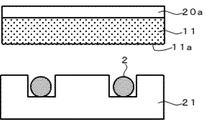
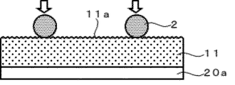
- the filler-containing film 1A can be manufactured as follows. First, the step of forming the insulating resin layer 11 by applying the above-described composition for forming an insulating resin layer containing a fine solid to a release substrate 20a having a smooth surface such as a PET film and drying it. Perform (FIG. 2A).
- the concave portion of the mold 21 in which the concave portion is formed corresponding to the regular arrangement of the filler 2 is filled with the filler 2 (FIG. 2B), transferring to the dry surface (surface opposite to the peeling substrate 20a) 11a of the insulating resin layer 11 (FIG. 2C), and performing a step of pushing the filler 2 into the insulating resin layer 11 (FIG. 2D). ).
- the insulating resin layer 12 is formed on the peeling base material 20b in the same manner as the insulating resin layer 11, and the insulating resin layer 12 and the insulating resin layer 11 into which the above-mentioned filler is pressed are used.
- the peeling base materials 20a and 20b are opposed to each other (FIG. 2E), and a step of laminating them is performed (FIG. 2F).
- a filler-containing film 1A can be obtained (FIG. 1A).
- the filler 2 flows non-uniformly by thermocompression bonding, and the arrangement of the filler 2 after thermocompression bonding is an expansion of the original regular arrangement uniformly. Therefore, when the filler-containing film 1A is sandwiched between smooth surfaces and the area is subjected to thermocompression bonding under a predetermined heating and pressing condition according to the composition of the insulating resin layer, the repetition pitch of the filler after thermocompression bonding before thermocompression bonding The ratio is within 300%, which is significantly smaller than when the dry surfaces 11a and 12a of the insulating resin layer constitute the surface of the filler-containing film.
- thermocompression bonding conditions in which the ratio of the repetition pitch of the filler is within 300%, the temperature, pressure, and time can be easily selected because they can be appropriately selected from normal heating and pressing conditions in the insulating resin layer. Can do.
- a glass plate or the like As a smooth surface for sandwiching the filler-containing film when examining the ratio of the filler repeated pitch before and after thermocompression bonding, a glass plate or the like can be used, but the smooth surface of the article to be subjected to thermocompression bonding of the filler-containing film is used. May be.
- the filler-containing film is configured as an anisotropic conductive film
- smooth surfaces such as electrodes and bumps to be connected can be used. Thereby, the ratio of the repetition pitch of the conductive particles before and after thermocompression bonding in the electronic component to be connected can be evaluated.
- the area of the smooth surface when examining the ratio of the repeated pitches of the filler before and after thermocompression may be an area where the filler arrangement can be confirmed.
- the area can be an area in which at least one unit lattice or a repeating unit of a specific shape exists.
- the area where the unit cell is preferably 3 or more, more preferably 5 or more, and even more preferably 10 or more in the arrangement axis with the smallest filler pitch.
- the distance between the repeating units existing at the center is measured as the repetition pitch.
- the number of fillers is preferably 1000 or less, more preferably 500 or less, still more preferably 200 or less, and particularly preferably 50 or less. The area included in.
- the filler-containing film is configured as an anisotropic conductive film, and when evaluating the ratio of the repeated pitch of the conductive particles before and after thermocompression bonding, the smooth surface is, for example, a COG connection It is possible to use an input terminal having a relatively large area of the electronic component that performs the above. If the electronic component to be connected does not have a terminal having such an area, the evaluation may be performed using an electronic component having a terminal having such an area. As an example, a smooth surface of a terminal having a minimum one side of 30 ⁇ m or more, preferably 40 ⁇ m or more is used.
- N number The number of repeated pitch measurements (N number) is preferably 50 or more, and more preferably 100 or more. However, since such N number is difficult depending on the number density of the filler, it may be less.
- the measurement direction of the repetition pitch is a direction in which the ratio of the repetition pitch before and after the thermocompression bonding is increased.
- the actual repeat pitch ratio can be made equal to or less than the measured pitch ratio, and the accuracy of the filler arrangement can be confirmed.
- measurement points may be obtained by sampling in each measurement region. For example, 10% of the predetermined N number is measured in one region, and 10% of the N number is similarly measured in the other nine regions, and these are averaged. The number of regions where N number and N number are measured can be appropriately adjusted depending on the object to be thermocompression bonded.
- the amount of movement of the conductive particles may differ between the terminal flow direction and the direction perpendicular thereto. In this case, it is preferable to measure the pitch in the direction in which the amount of movement of the conductive particles is large.
- the terminal size and the distance between the terminals are large, and the amount of movement of the conductive particles in the terminal arrangement direction and the amount of movement of the conductive particles in the direction perpendicular thereto It is preferable to measure a pitch by selecting a portion having a small difference from the pitch. For example, in the case of COG connection, the terminal size and the distance between terminals are different between the input terminal and the output terminal. In that case, the pitch is measured at an input terminal having a large terminal size or a large distance between terminals. Thereby, it becomes easy to evaluate the movement amount of the conductive particles and the disorder of the arrangement.
- the above-described pitch measurement direction, measurement site, etc. when examining the ratio of the repeated pitch of the filler before and after thermocompression bonding can be the same even if the filler-containing film is other than the anisotropic conductive film.
- the ratio of the filler repeating pitch before and after thermocompression bonding with the article to be connected if the article does not have a smooth surface, it can be replaced with smooth glass plates.
- pitch measurement means examples include known image observation apparatuses such as an optical microscope, a metal microscope, and an electron microscope, and measurement systems such as WinROOF and A Image-kun (registered trademark), which can be appropriately combined.
- the smoothness of the surface is improved and the adhesiveness to the article is improved, so that the ratio of the repeated pitch of the filler after thermocompression bonding before thermocompression bonding is 300% as described above.
- the following can be reduced. Therefore, when the filler-containing film 1A is configured as an anisotropic conductive film, the temporary press bonding property of the anisotropic conductive film to the electronic component is improved, and the trapping property of the conductive particles at the terminal of the electronic component is improved also in the main press bonding. Short circuit is suppressed. Therefore, even when the terminal size of the electronic component is narrowed, it is possible to reliably conduct and suppress a short circuit.
- the improved adhesiveness stabilizes the mounting of electronic components that can be connected to both large and small electronic components, facilitates the manufacture of connectors, and improves productivity. it can.
- the need for precise alignment increases, so the filler-containing film of the present invention has a great effect.
- the filler-containing film of the present invention can take various forms.
- the filler-containing film 1B shown in FIG. 3 has a position on the film surface side of the filler 2 and the surface of the filler-containing film 1B (on the peeling substrate side of the insulating resin layer 12) with respect to the filler-containing film 1A described above. The difference is that the surface 12b) is flush with the film thickness direction.
- This filler-containing film 1B is a step of forming insulating resin layers 11 and 12 formed on the release substrates 20a and 20b (FIG. 4A), respectively, in the same manner as the manufacturing method of the filler-containing film 1A.
- 12 are laminated with the peeling base materials 20a and 20b on the outside (FIG. 4B), one peeling base material 20b is peeled, and the insulating resin after peeling is formed. It can manufacture by performing the process of pushing in the filler 2 from the surface 12b of the layer 12 (FIG. 4C).
- the surfaces 11b and 12b of the insulating resin layer forming the surface are smooth because the smoothness of the surfaces of the peeling base materials 20a and 20b is transferred, and is the same as the filler-containing film 1A. Demonstrate the effect.
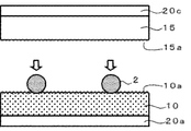
- the filler-containing film 1C shown in FIG. 5 is obtained by laminating a low-viscosity resin layer 15 on the filler pressing surface (the surface 12b of the insulating resin layer on the peeling substrate side) (FIG. 4C) of the filler-containing form 1B. Is.
- the low viscosity resin layer 15 is a resin layer having a minimum melt viscosity in the range of 30 to 200 ° C. lower than that of the insulating resin layer 10.
- the low-viscosity resin layer 15 By laminating the low-viscosity resin layer 15 on the insulating resin layer 10, when two articles facing each other through the filler-containing film 1C are thermocompression bonded, their adhesiveness can be improved.
- 2 is used as conductive particles
- the filler-containing film 1C is used as an anisotropic conductive film, and when an electronic component is anisotropically conductively connected, the space formed by the electrodes and bumps of the electronic component is filled with the low-viscosity resin layer 15 And the adhesiveness of electronic components can be improved.
- the space between two articles connected via the filler-containing film 1C is filled with the low-viscosity resin layer 15 as the difference between the minimum melt viscosity of the insulating resin layer 10 and the minimum melt viscosity of the low-viscosity resin layer 15 increases. It becomes easy to be done. For this reason, when using the filler 2 as conductive particles and using the filler-containing film 1C as an anisotropic conductive film, the space formed by the electrodes and bumps of the electronic component is easily filled with the low-viscosity resin layer 15, It becomes easy to improve the adhesiveness between electronic components.
- the ratio (A1 / A2) of the minimum melt viscosity A1 of the insulating resin layer 10 and the minimum melt viscosity A2 of the low viscosity resin layer 15 is practically the ratio of the layer thickness of the insulating resin layer 10 and the low viscosity resin layer 15 However, it is preferably 2 or more, more preferably 5 or more, and still more preferably 8 or more. On the other hand, when this ratio is too large, when a long filler-containing film is used as a wound body, there is a possibility that the resin protrudes or blocks, and therefore, practically, 30 or less is preferable, and 15 or less is more preferable.
- the preferable minimum melt viscosity of the low-viscosity resin layer 15 more specifically satisfies the above-mentioned ratio, and is 3000 Pa ⁇ s or less, more preferably 2000 Pa ⁇ s or less, and particularly preferably 100 to 2000 Pa ⁇ s. .
- the low-viscosity resin layer 15 can be formed by adjusting the viscosity in the same resin composition as the insulating resin layer 10.
- the low-viscosity resin layer 15 can contain a fine solid as necessary.
- a composition for forming a low-viscosity resin layer is formed on a release substrate 20c such as a release film.
- the low-viscosity resin layer 15 is formed by coating and drying, and the dry surface 15a is opposed to the pressing surface of the filler 2 of the insulating resin layer 10, and the low-viscosity resin layer 15 is laminated on the insulating resin layer 10. be able to.
- the content of fine solids in the low-viscosity resin layer 15 is low and there is no substantial difference between the adhesiveness of the dry surface 15a of the low-viscosity resin layer 15 and the adhesiveness of the surface 15b on the opposite side. May apply the composition for low-viscosity resin layer formation directly to the pressing surface of the filler 2 of the insulating resin layer 10 to form the low-viscosity resin layer 15.
- the top of the filler 2 is flush with the outer surface of the insulating resin layer 10 of the laminate in which the dry surfaces of the insulating resin layer 10 and the low-viscosity resin layer 15 face each other. They are arranged together and can be manufactured from the next step.
- a composition for forming an insulating resin layer containing a minute solid is applied on the release substrate 20a and dried to form the insulating resin layer 10, and a composition for forming a low-viscosity resin layer is formed.
- An object is applied on the peeling substrate 20c and dried to form a low-viscosity resin layer 15 (FIG. 8A).
- the insulating resin layer 10 and the low-viscosity resin layer 15 are combined with each other.
- a step of forming a laminate of the insulating resin layer 10 and the low-viscosity resin layer 15 is performed by laminating the peeling base materials 20a and 20c outside (that is, with the dry surfaces facing each other) (FIG. 8B).
- the peeling substrate 20a of the insulating resin layer 10 is peeled from the laminate, and the filler 2 is pushed in from the surface of the insulating resin layer from which the peeling substrate is peeled (FIG. 8C).
- the surface 10b of the insulating resin layer and the surface 15b of the low-viscosity resin layer 15 forming the surfaces thereof are transferred by the smoothness of the surfaces of the release substrates 20a and 20c. It is smooth and exhibits the same effect as the filler-containing film 1A.
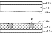
- the filler-containing film 1E shown in FIG. 9 has the top of the filler 2 on the dry surface of the insulating resin layer 10 of the laminate in which the dry surface of the insulating resin layer 10 and the dry surface of the low-viscosity resin layer 15 face each other. They are arranged flush with each other and can be manufactured from the next step.
- an insulating resin layer-forming composition containing fine solids is applied onto the release substrate 20a and dried to dry the insulating resin layer. 10 is performed, and the low-viscosity resin layer forming composition is applied onto the peeling substrate 20c and dried to form the low-viscosity resin layer 15 (FIG. 8A).
- the filler 2 is pushed into the dry surface 10a of the insulating resin layer 10 by performing a step of pushing the filler 2 from the surface (dry surface 10a) opposite to the release substrate 20a of the insulating resin layer 10 (FIG. 10A).
- the tops in the film thickness direction of 2 are flush with each other (FIG. 10B).
- the dry surface 10a and the dry surface 15a of the low-viscosity resin layer described above are laminated so as to face each other (FIG. 10C).
- the surface 10b of the insulating resin layer and the surface 15b of the low-viscosity resin layer 15 forming the surface are also smooth because the smoothness of the surfaces of the release substrates 20a and 20c is transferred. And exhibits the same effect as the filler-containing film 1A.
- the filler-containing film can be a wound body in its product form.
- it is 5000 m or less, More preferably, it is 1000 m or less, More preferably, it is 500 m or less. On the other hand, 5 m or more is preferable from the viewpoint of mass productivity of the wound body.
- the wound body may be formed by connecting filler-containing films shorter than the entire length.
- a connection place can exist in multiple places regularly or randomly.
- the film width in the wound body it is preferable to make the film width 0.3 mm or more from the lower limit of the slit width when slitting a wide filler-containing film to produce a wound body, More preferably, the slit width is 0.5 mm or more from the viewpoint of stabilizing the slit width.
- the slit width is 0.5 mm or more from the viewpoint of stabilizing the slit width.
- the film width is preferably selected from 0.3 to 400 mm depending on the connection object from the viewpoint of practical handling. That is, when an anisotropic conductive film is used at the end of an electronic article to be connected, the film width is often set to about several millimeters or less, and relatively large electronic components (electrode wiring and mounting portion are on one side). In the case where the film is used as it is attached to a substrate or a wafer before cutting), a film width of about 400 mm may be required. Generally, the anisotropic conductive film is often used with a film width of 0.5 to 5 mm.
- the filler-containing film of the present invention can be used by being attached to an article similarly to the conventional filler-containing film, and the article to be attached is not particularly limited. Therefore, various 1st components and 2nd components can be connected via a filler containing film, and the connection body of a 1st article and a 2nd article can be obtained.
- the anisotropic conductive film is converted into a semiconductor element using a PN junction using a thermocompression bonding tool (power generation element such as a solar cell, imaging element such as a CCD, Light-emitting elements, Peltier elements), other various semiconductor elements, IC chips, IC modules, FPCs and other first electronic components, and FPCs, glass substrates, plastic substrates, rigid substrates, ceramic substrates and other second electronic components
- a thermocompression bonding tool power generation element such as a solar cell, imaging element such as a CCD, Light-emitting elements, Peltier elements
- This filler-containing film can also be used for electronic parts for purposes other than anisotropic conductive connection.
- the surface of the article on which the filler-containing film is bonded may be smooth or may have a stepped portion or a convex shape.
- a filler containing film when using it for large sized TV etc., may be stuck 1 m or more, for example, 4.5 m or more to one side.
- the filler-containing film in addition to using the filler-containing film as an anisotropic conductive film, it may be used as a spacer film using a filler as a spacer.
- the IC chip or wafer may be stacked to make a multilayer by using the anisotropic conductive film of the present invention.
- the electronic component connected with the anisotropic conductive film of this invention is not limited to the illustration of the above-mentioned electronic component. It can be used for various electronic parts that have been diversified in recent years.
- the present invention includes a film adhesive body in which the filler-containing film of the present invention is bonded to various articles, and in particular, a connection in which the first electronic component and the second electronic component are connected via an anisotropic conductive film. Includes the body.
- the method for laminating the filler-containing film to the article may be pressure bonding, preferably thermocompression bonding depending on the use of the filler-containing film, and light irradiation may be used at the time of bonding.
- the first electronic component is an IC chip and the second electronic component is a substrate
- the first electronic is generally used.
- the component is placed on the pressure tool side
- the second electronic component is placed on the stage facing the first electronic component
- an anisotropic conductive film is pasted on the second electronic component in advance, and the first using the pressure tool.
- Thermocompression bonding of the electronic component and the second electronic component is performed.
- an anisotropic conductive film may be attached in advance to the first electronic component, and the first electronic component is not limited to the IC chip.
- the resin around the conductive particles may be removed in advance before the thermocompression bonding. Thereby, the influence of the resin flow generated when the anisotropic conductive film is thermocompression bonded to the electronic article can be reduced, and unnecessary flow of the conductive particles can be suppressed.
- thermocompression bonding as the main pressure bonding (hereinafter, not only the thermocompression bonding during the main pressure bonding).
- a connection method in which pressing is performed even by provisional pressure bonding is called connection by two-step pressing).
- WO2016 / 143789 describes that the connection is made by two-step indentation using an anisotropic conductive film in which conductive particles are randomly dispersed, but the conductive particles are regularly arranged as in the present invention.
- the number of these is not limited to one-to-one.
- a plurality of first electronic components are connected to one second electronic component.
- the present invention also includes a method for manufacturing a connection body in which the first electronic component and the second electronic component are connected via an anisotropic conductive film.
- Comparative Example 1 (1) Formation of Insulating Resin Layer An insulating resin layer forming composition is prepared with the formulation shown in Table 1, applied to a PET film, dried, and the insulating resin layer having the thickness shown in Table 2 (hereinafter, high viscosity) Resin layer).
- the metal-coated resin particles (Sekisui Chemical Co., Ltd., AUL703, average particle diameter 3 ⁇ m) described in Examples of Patent Document 5 are used as the conductive particles.
- the conductive particles were pressed into the dry surface of the high-viscosity resin layer by the method described in the Example of (1), which was adhered to the dry surface of the high-viscosity resin layer and pressed (60 ° C., 0.5 MPa). (Particle density 28000 / mm 2 ). In this case, the conductive particles were arranged in a hexagonal lattice, and the top in the film thickness direction was flush with the dry surface of the high viscosity resin layer.
- Example 1 A high viscosity resin layer was formed on the PET film in the same manner as in Comparative Example 1 (layer thickness: 3 ⁇ m).
- a composition for forming a low-viscosity resin layer was prepared with the formulation shown in Table 1, and applied to a PET film and dried to form a low-viscosity resin layer having a layer thickness of 3 ⁇ m.
- Minimum melt viscosity of this low-viscosity resin layer (rotary rheometer (manufactured by TA instruments), measurement pressure 5 g, temperature range 30 to 200 ° C., heating rate 10 ° C./min, measurement frequency 10 Hz, measurement plate diameter 8 mm, measurement plate The load fluctuation 5 g) was 300 Pa ⁇ s.
- the high-viscosity resin layer on the PET film and the low-viscosity resin layer on the PET film are bonded to each other to form a laminate of the high-viscosity resin layer and the low-viscosity resin layer.
- conductive particles were stuck and pressed into the surface of the high viscosity resin layer from which the PET film was peeled.
- Example 2 A high viscosity resin layer was formed on a PET film in the same manner as in Comparative Example 1, and conductive particles were pushed into the dried surface. On the other hand, a low-viscosity resin layer was formed on a PET film in the same manner as in Example 1, and this dry surface was bonded to the dry surface of the high-viscosity resin layer.
- Example 3 A high-viscosity resin layer was formed on the PET film in the same manner as in Comparative Example 1 (layer thickness 3 ⁇ m), and conductive particles were pushed in from the dried surface. Separately, a high-viscosity resin layer was separately formed on the PET film (layer thickness 3 ⁇ m), and the dry surfaces of both high-viscosity resin layers were bonded together.
- Example 4 A high viscosity resin layer was formed on the PET film in the same manner as in Comparative Example 1 (layer thickness: 3 ⁇ m). A similar high-viscosity resin layer was separately formed (layer thickness: 3 ⁇ m), and these dry surfaces were bonded together to form a laminate having two high-viscosity resin layers. One PET film of this laminate was peeled off, and conductive particles were stuck and pressed into the surface of the high viscosity resin layer from which the PET film was peeled in the same manner as in Comparative Example 1.
- Ratio of repeated pitch of particle arrangement before and after thermocompression bonding (%)
- the following electronic parts (a) and (b) are used as electronic parts for evaluation of the ratio of the repetition pitch of the particle arrangement before and after thermocompression bonding, and these electronic parts (a) and (b) are produced in examples and comparative examples.
- the bump area (0.0024 mm 2 ) containing at least 50 conductive particles was sandwiched by thermocompression bonding at a temperature of 180 ° C. and a pressure of 60 MPa for 5 seconds.
- the glass substrate of the electronic component (b) was disposed on the lower side in the figure, and the evaluation IC for the electronic component (a) was disposed on the upper side.
- the repetition pitch P0 of the conductive particles before thermocompression bonding and the repetition pitch P1 (distance between the centers of the conductive particles) (FIG. 1) of the conductive particles after thermocompression bonding are expressed by two axes per bump at the center of the bump area. Measured. That is, the axis having the shallowest angle (near parallel) with respect to the bump arrangement direction and a small movement amount of the resin (A axis) and the axis having the largest angle with respect to the bump arrangement direction and the large movement amount of the resin (B axis). ), The pitch P0 before thermocompression bonding was measured.
- This measurement was performed with 20 or more bumps in parallel, and the number of measurements for each of the A-axis and B-axis was set to 50, and the average of the pitches P0 was obtained for each axis.
- the pitch P1 after thermocompression bonding the number of measurements was set to 50 for each of the A axis and the B axis, and the average of the pitch P1 for each axis was obtained.
- the ratio ((P1 / P0) ⁇ 100%) before and after thermocompression bonding was determined for each of the A axis and B axis.
- Evaluation criteria OK The anisotropic conductive film does not peel from the glass substrate in all 100 times.
- NG The anisotropic conductive film peels from the glass substrate at least once out of 100 times.
- Example 1 and Example 2 when placed on a flat surface and the touch was confirmed with a finger, the adhesive force on the low viscosity resin layer side was larger than the adhesive force on the high viscosity resin layer side.
- the lower slide glass 30 is placed on a hot plate heated to 40 to 50 ° C., which is a general stage temperature for temporary attachment at the time of mounting, is pressed with a finger, heated for 30 seconds, and bonded together.
- the slide glass 30 and the lower surface of the anisotropic conductive film were in a so-called temporarily attached state.
- the upper slide glass 31 is placed on and bonded to the upper surface of the “film configuration” shown in Table 2, and the upper slide glass 31 is adhered by the adhesive force of the upper surface of the anisotropic conductive film. It was in the state.
- the lower slide glass 30 is fixed with a jig using an AGS-X series manufactured by Shimadzu Corporation.
- the value was divided by the area of the anisotropic conductive film 1 to obtain the adhesive strength of the upper surface of “Film Configuration” in Table 2.
- the adhesive strength test was performed twice, and the minimum value is shown in Table 2.
- a cylindrical 5 mm diameter probe (stainless steel mirror finish) of a tack tester is set above the measurement surface, and the probe is brought into contact with the measurement surface at a pressing speed of 30 mm / min, and a pressure of 196.25 gf is applied.
- the pressure is applied for 1.0 sec, the resistance that the probe receives due to the adhesive force of the measurement surface when it is peeled 2 mm from the measurement surface at a peeling speed of 120 mm / min is measured as a load value, and the probe is peeled off from the measurement surface
- the maximum load was the adhesive force (tack force).
- the adhesive strength was measured twice, and the minimum value is shown in Table 2. However, since the measurement in Examples 3 and 4 was difficult, the variation in measured values was larger than that in Examples 1 and 2. In Comparative Example 1, the adhesive strength was smaller than that in Examples 3 and 4 due to the touch feeling with a finger, and measurement was not performed.
- Examples 1 to 4 are superior to Comparative Example 1 in (2) film surface adhesion (temporary pressure bonding test).
- Examples 1 to 4 and Comparative Example 1 it can be seen that (3) initial conduction resistance and (4) conduction reliability are not problematic in Examples 1 to 4.
- the ratio of the pitch before and after thermocompression bonding ((P1 / P0) ⁇ 100%) on both the A axis and the B axis is 300% or less, and the arrangement before and after thermocompression bonding It was confirmed that there was little disturbance.
- the bumps and terminal patterns of the evaluation IC chip and the glass substrate correspond to each other. Moreover, when connecting the IC chip for evaluation and the glass substrate, the longitudinal direction of the anisotropic conductive film and the arrangement direction of the bumps were matched. In the two-step indentation, the temporary pressure bonding was performed at 80 ° C. for 3 seconds, and the final pressure bonding was performed at 180 ° C. for 10 seconds at twice the pressure of the temporary pressure bonding. In proceeding from the temporary pressure bonding to the main pressure bonding, the pressure applied to the evaluation IC chip was increased without releasing the pressure.
- a flip chip bonder (Panasonic FCB3, with pal heater) was used, and the temperature was raised to 0.5 seconds and the pressure was raised to 0.5 seconds in both the temporary pressure bonding and the main pressure bonding. Moreover, the connection body which performed only said main crimping
- connection body that was not pressed by the temporary pressure bonding was pressed in two steps (the pressure was increased without releasing the pressure after the temporary pressure bonding). It was confirmed that there are many conductive particles sandwiched per one.
Landscapes
- Chemical & Material Sciences (AREA)
- Organic Chemistry (AREA)
- Inorganic Chemistry (AREA)
- Engineering & Computer Science (AREA)
- Manufacturing & Machinery (AREA)
- Laminated Bodies (AREA)
Abstract
絶縁性樹脂層10にフィラー2と微小固形物3が保持され、平面視でフィラー2が所定配列を繰り返しているフィラー含有フィルム1Aは、該フィラー含有フィルム1Aを平滑面で挟み、所定の熱圧着条件で熱圧着した場合の、熱圧着前に対する熱圧着後のフィラーの繰り返しピッチの比率が300%以内である。このフィラー含有フィルム1Aの一つの製造方法は、剥離基材20a上に絶縁性樹脂層11を形成する工程、絶縁性樹脂層11の剥離基材20aと反対側の面からフィラー2を押し込む工程、フィラー2を押し込んだ絶縁性樹脂層11と、該絶縁性樹脂層と別個の絶縁性樹脂層12とをそれらの剥離基材20a、20bを外側にして積層する工程を有する。このフィラー含有フィルム1Aによれば、該フィルム1Aを物品に熱圧着した場合のフィラー配列の乱れが抑制される。
Description
本発明は、フィラー含有フィルムに関する。
フィラーが樹脂層に分散しているフィラー含有フィルムは、艶消しフィルム、コンデンサー用フィルム、光学フィルム、ラベル用フィルム、耐電防止用フィルム、導電フィルム、異方性導電フィルムなど多種多様の用途で使用されている(特許文献1、特許文献2、特許文献3、特許文献4)。フィラー含有フィルムを物品に熱圧着して用いる場合、フィラー含有フィルムを形成している樹脂が熱圧着時に不用に流動することを抑制し、フィラーの偏在を抑制することが、光学的特性、機械的特性、又は電気的特性の点から望ましい。特に、フィラーとして導電粒子を含有させ、フィラー含有フィルムを電子部品の実装に供する異方性導電フィルムとして使用する場合に、電子部品の高密度実装に対応できるように、絶縁性樹脂層に導電粒子を高密度に分散させると、電子部品の実装時の樹脂流動により導電粒子が不用に移動して端子間に偏在し、ショートの発生要因となるので、このような樹脂流動を抑制することが望ましい。
これに対し、絶縁性樹脂層に溶融粘度調整剤やチキソトロピック剤といった微小固形物を含有させることが行われている(特許文献5、6)。
また、絶縁性樹脂層に導電粒子を高密度に分散させた場合の電子部品の端子における導電粒子の捕捉性の向上とショートの抑制を両立させるため、導電粒子を規則的に配置することが行われている(特許文献5、6)。
微小固形物を含有する絶縁性樹脂層は、一般に、微小固形物を分散させた絶縁性樹脂層形成用組成物の塗布乾燥により形成される。しかしながら、微小固形物を高濃度に含有する絶縁性樹脂層を、絶縁性樹脂層形成用組成物の塗布乾燥によって形成する場合、絶縁性樹脂層の乾燥面(即ち、絶縁性樹脂層形成用組成物の塗布層において、該組成物に含まれる溶媒が蒸発していく面)に微小固形物に由来する荒れが形成されるためか、絶縁性樹脂層の粘着性が低下し、電子部品の実装時の仮圧着が均一に行われず、貼着状態が安定しなくなる。また、本圧着時の熱圧着も均一に行われず、絶縁性樹脂層に規則的に配列していた導電粒子に配列の乱れが生じ、電子部品の端子における導電粒子の捕捉性の向上やショートの抑制に悪影響がもたらされる虞が生じる。この問題は、特に電子部品が小型で端子サイズが狭小化している場合に顕著となる。また、フィラー含有フィルム表面の粘着性の低下の問題は、フィルム厚を薄くすると厚い場合に比して顕著になる場合もある。
これに対し、本発明は、絶縁性樹脂層に微小固形物が適度な配合量で分散され、該絶縁性樹脂層に導電粒子等のフィラーが所定の配列を繰り返すことにより規則的に配列しているフィラー含有フィルムにおいて、フィラー含有フィルムを物品に熱圧着した場合のフィラーの配列の乱れを抑制することを課題とする。
本発明者は、導電粒子等のフィラーと、該フィラーとは形成素材の異なる微小固形物とが絶縁性樹脂層に保持されているフィラー含有フィルムを、微小固形物を含有する絶縁性樹脂層形成用組成物の塗布により絶縁性樹脂層を形成する工程と、絶縁性樹脂層にフィラーを押し込む工程により製造する場合に、フィラー含有フィルムの表面に、絶縁性樹脂層の乾燥面が現れないようにすると、フィラー含有フィルムを物品に熱圧着したときのフィラーの配列の乱れが低減することを見出し、本発明を完成した。
即ち、本発明は、絶縁性樹脂層にフィラーと、フィラーと形成素材の異なる微小固形物が保持され、平面視でフィラーが所定配列を繰り返しているフィラー含有フィルムであって、
フィラー含有フィルムを平滑面で挟み、所定の熱圧着条件で熱圧着した場合の、熱圧着前に対する熱圧着後のフィラーの繰り返しピッチの比率が300%以内であるフィラー含有フィルムを提供し、特に、絶縁性樹脂層が2層の絶縁性樹脂層の積層体から形成されている態様及び、30~200℃の範囲の最低溶融粘度が絶縁性樹脂層よりも低い低粘度樹脂層が絶縁性樹脂層に積層されている態様を提供する。
フィラー含有フィルムを平滑面で挟み、所定の熱圧着条件で熱圧着した場合の、熱圧着前に対する熱圧着後のフィラーの繰り返しピッチの比率が300%以内であるフィラー含有フィルムを提供し、特に、絶縁性樹脂層が2層の絶縁性樹脂層の積層体から形成されている態様及び、30~200℃の範囲の最低溶融粘度が絶縁性樹脂層よりも低い低粘度樹脂層が絶縁性樹脂層に積層されている態様を提供する。
また、本発明は、このフィラー含有フィルムの第1の製造方法として、微小固形物を含有する絶縁性樹脂層形成用組成物を剥離基材上に塗布し、剥離基材上に絶縁性樹脂層を形成する工程、
絶縁性樹脂層の剥離基材と反対側の面からフィラーを押し込む工程、
フィラーを押し込んだ絶縁性樹脂層と、該絶縁性樹脂層と別個の絶縁性樹脂層とをそれらの剥離基材を外側にして積層する工程、
を有するフィラー含有フィルムの製造方法を提供し、
第2の製造方法として、微小固形物を含有する絶縁性樹脂層形成用組成物を剥離基材上に塗布し、剥離基材上に絶縁性樹脂層を形成する工程、
2つの絶縁性樹脂層を、それらの剥離基材を外側にして積層することにより絶縁性樹脂層の積層体を形成する工程、
該絶縁性樹脂層の積層体にフィラーを押し込む工程、
を有するフィラー含有フィルムの製造方法を提供し、
第3の製造方法として、微小固形物を含有する絶縁性樹脂層形成用組成物を剥離基材上に塗布し、剥離基材上に絶縁性樹脂層を形成する工程、
30~200℃の範囲の最低溶融粘度が絶縁性樹脂層より低い低粘度樹脂層の形成用組成物を剥離基材に塗布し、剥離基材上に低粘度樹脂層を形成する工程、
絶縁性樹脂層と低粘度樹脂層を、それらの剥離基材を外側にして積層することにより絶縁性樹脂層と低粘度樹脂層の積層体を形成する工程、
絶縁性樹脂層の剥離基材を剥離し、剥離基材を剥離した絶縁性樹脂層の面からフィラーを押し込む工程、
を有するフィラー含有フィルムの製造方法を提供し、
第4の製造方法として、微小固形物を含有する絶縁性樹脂層形成用組成物を剥離基材上に塗布し、剥離基材上に絶縁性樹脂層を形成する工程、
30~200℃の範囲の最低溶融粘度が絶縁性樹脂層より低い低粘度樹脂層の形成用組成物を剥離基材に塗布し、剥離基材上に低粘度樹脂層を形成する工程、
絶縁性樹脂層の剥離基材と反対側の面にフィラーを押し込む工程、
フィラーを押し込んだ絶縁性樹脂層と、剥離基材上に形成した低粘度樹脂層とを、それらの剥離基材を外側にして積層する工程、
を有するフィラー含有フィルムの製造方法を提供する。
本発明のフィラー含有フィルムの製造方法によれば、絶縁性樹脂層に微小固形物が粘度調整等の点から適度な配合量で含有されているにも関わらず、フィラー含有フィルムの表面に荒れが形成されないためか、フィルム表面が種々の物品に対して良好な粘着性を有する。したがって、物品に熱圧着により貼り付けたフィラー含有フィルムのフィラーは、熱圧着前の所定配列をほぼ維持することができる。
例えば、本発明のフィラー含有フィルムのフィラーが導電粒子である場合に、本発明のフィラー含有フィルムを電子部品同士の異方性導電接続に使用すると、仮圧着を良好に行うことができ、本圧着でも導電粒子の配列に乱れが起こりにくいため、熱圧着前の所定配列をほぼ維持することができる。よって、電子部品が小型で端子サイズが狭小化している場合でも電子部品同士を良好に異方性導電接続することができる。
以下、本発明のフィラー含有フィルムの一例について図面を参照しつつ詳細に説明する。なお、各図中、同一符号は、同一又は同等の構成要素を表している。
<フィラー含有フィルム1Aの全体構成>
図1Aは実施例のフィラー含有フィルム1Aのフィラー配置を示す平面図であり、図1BはそのX-X断面図である。このフィラー含有フィルム1Aは、フィラー2として導電粒子を含有し、異方性導電フィルムとして使用されるもので、絶縁性樹脂層10に導電粒子が所定配列を繰り返す規則的な配置で保持されている。絶縁性樹脂層10は、フィラー2の他に微小固形物3を含有している。従来のフィラー含有フィルムを、後述するように平滑面で挟んで熱圧着した場合、熱圧着前の規則的なフィラーの配置は熱圧着後に広がり、配列の繰り返しピッチは熱圧着前に対して広くなり、繰り返しピッチのバラツキも大きくなり、フィラーの配列に乱れが生じるが、本発明のフィラー含有フィルムでは、フィラーの移動量や配列の乱れが少なく、熱圧着前に対する熱圧着後のフィラーの繰り返しピッチの比率が300%以内、好ましくは250%以内、より好ましくは200%以内である。言い換えると、本発明のフィラー含有フィルムによれば熱圧着前後でフィラー配置の相対的位置関係が維持されることにより熱圧着前の最近接フィラーの中心間距離に対して、熱圧着後の最近接フィラーの中心間距離を3倍以内、2.5倍以内、2倍以内にすることができる。
図1Aは実施例のフィラー含有フィルム1Aのフィラー配置を示す平面図であり、図1BはそのX-X断面図である。このフィラー含有フィルム1Aは、フィラー2として導電粒子を含有し、異方性導電フィルムとして使用されるもので、絶縁性樹脂層10に導電粒子が所定配列を繰り返す規則的な配置で保持されている。絶縁性樹脂層10は、フィラー2の他に微小固形物3を含有している。従来のフィラー含有フィルムを、後述するように平滑面で挟んで熱圧着した場合、熱圧着前の規則的なフィラーの配置は熱圧着後に広がり、配列の繰り返しピッチは熱圧着前に対して広くなり、繰り返しピッチのバラツキも大きくなり、フィラーの配列に乱れが生じるが、本発明のフィラー含有フィルムでは、フィラーの移動量や配列の乱れが少なく、熱圧着前に対する熱圧着後のフィラーの繰り返しピッチの比率が300%以内、好ましくは250%以内、より好ましくは200%以内である。言い換えると、本発明のフィラー含有フィルムによれば熱圧着前後でフィラー配置の相対的位置関係が維持されることにより熱圧着前の最近接フィラーの中心間距離に対して、熱圧着後の最近接フィラーの中心間距離を3倍以内、2.5倍以内、2倍以内にすることができる。
本発明のフィラー含有フィルムは、熱圧着前後での繰り返しピッチの比率が上述の数値以下になる熱圧着条件を有している。これは、本発明のフィラー含有フィルムの製造方法によれば、フィラー含有フィルム1Aの表面が剥離基材からの剥離面となるため、絶縁性樹脂層10が微小固形物3を多量に含有していてもフィラー含有フィルム1Aの表面が荒れず、平滑面となり、その平滑面を物品に貼着して加熱加圧すると、フィラー含有フィルムが一様に押圧され、フィルム内で規則的に配列しているフィラーに押圧力が均一に加わることを微小固形物が阻害せず、フィラーの配列が不均一に乱れることが抑制され、加熱加圧後のフィラーの配置が当初の配列を一様に伸張したものとなり、熱圧着前後のフィラーの繰り返しピッチの比率が局部的に大きくなる部分が低減するためと考えられる。
なお、この熱圧着によるフィラーの移動量や配列の乱れの少なさは、フィラー含有フィルムを構成する樹脂層の層厚を薄くすることにより一層顕著となる。
また、熱圧着が平滑面で行われない場合には熱圧着によるフィラーの移動量や配列の乱れに不均一性が生じる。そのため、フィラー含有フィルムを異方性導電フィルムとして構成した場合に、異方性導電フィルムでファインピッチのバンプ配列を熱圧着すると、フィラー配列の乱れが比較的大きくなることがある。
<フィラー>
本発明においてフィラー2としては、フィラー含有フィルムの用途に応じて、公知の無機系フィラー(金属粒子、金属酸化物粒子、金属窒化物粒子など)、有機系フィラー(樹脂粒子、ゴム粒子など)、有機系材料と無機系材料が混在したフィラー(例えば、コアが樹脂材料で形成され、表面が金属メッキされている粒子(金属被覆樹脂粒子)、導電粒子の表面に絶縁性微粒子を付着させたもの、導電粒子の表面を絶縁処理したもの等)から、硬さ、光学的性能などの用途に求められる性能に応じて適宜選択される。例えば、光学フィルムや艶消しフィルムでは、シリカフィラー、酸化チタンフィラー、スチレンフィラー、アクリルフィラー、メラミンフィラーや種々のチタン酸塩等を使用することができる。コンデンサー用フィルムでは、酸化チタン、チタン酸マグネシウム、チタン酸亜鉛、チタン酸ビスマス、酸化ランタン、チタン酸カルシウム、チタン酸ストロンチウム、チタン酸バリウム、チタン酸ジルコン酸バリウム、チタン酸ジルコン酸鉛及びこれらの混合物等を使用することができる。接着フィルムではポリマー系のゴム粒子、シリコーンゴム粒子等を含有させることができる。導電フィルムや異方性導電フィルムでは導電粒子を含有させる。導電粒子としては、ニッケル、コバルト、銀、銅、金、パラジウムなどの金属粒子、ハンダなどの合金粒子、金属被覆樹脂粒子、表面に絶縁性微粒子が付着している金属被覆樹脂粒子などが挙げられる。2種以上を併用することもできる。中でも、金属被覆樹脂粒子が、接続された後に樹脂粒子が反発することで端子との接触が維持され易くなり、導通性能が安定する点から好ましい。また、導電粒子の表面には公知の技術によって、導通特性に支障を来さない絶縁処理が施されていてもよい。
本発明においてフィラー2としては、フィラー含有フィルムの用途に応じて、公知の無機系フィラー(金属粒子、金属酸化物粒子、金属窒化物粒子など)、有機系フィラー(樹脂粒子、ゴム粒子など)、有機系材料と無機系材料が混在したフィラー(例えば、コアが樹脂材料で形成され、表面が金属メッキされている粒子(金属被覆樹脂粒子)、導電粒子の表面に絶縁性微粒子を付着させたもの、導電粒子の表面を絶縁処理したもの等)から、硬さ、光学的性能などの用途に求められる性能に応じて適宜選択される。例えば、光学フィルムや艶消しフィルムでは、シリカフィラー、酸化チタンフィラー、スチレンフィラー、アクリルフィラー、メラミンフィラーや種々のチタン酸塩等を使用することができる。コンデンサー用フィルムでは、酸化チタン、チタン酸マグネシウム、チタン酸亜鉛、チタン酸ビスマス、酸化ランタン、チタン酸カルシウム、チタン酸ストロンチウム、チタン酸バリウム、チタン酸ジルコン酸バリウム、チタン酸ジルコン酸鉛及びこれらの混合物等を使用することができる。接着フィルムではポリマー系のゴム粒子、シリコーンゴム粒子等を含有させることができる。導電フィルムや異方性導電フィルムでは導電粒子を含有させる。導電粒子としては、ニッケル、コバルト、銀、銅、金、パラジウムなどの金属粒子、ハンダなどの合金粒子、金属被覆樹脂粒子、表面に絶縁性微粒子が付着している金属被覆樹脂粒子などが挙げられる。2種以上を併用することもできる。中でも、金属被覆樹脂粒子が、接続された後に樹脂粒子が反発することで端子との接触が維持され易くなり、導通性能が安定する点から好ましい。また、導電粒子の表面には公知の技術によって、導通特性に支障を来さない絶縁処理が施されていてもよい。
<フィラーの粒子径>
本発明においてフィラー2の粒子径はフィラー含有フィルムの用途に応じて定めることができる。例えば、フィラー含有フィルムを異方性導電フィルムとして使用する場合、フィラー含有フィルムの製造時のフィラーの押込精度を向上させるため、好ましくは1μm以上、より好ましくは2.5μm以上である。また、フィラー含有フィルムの製造時のフィラーの位置ずれの影響を抑制するため、好ましくは200μm以下、より好ましくは50μm以下である。ここで、粒子径は平均粒子径を意味する。フィラー含有フィルムにおけるフィラーの平均粒子径は、平面画像又は断面画像から求めることができる。また、フィラー含有フィルムに含有させる前の原料粒子としてのフィラーの平均粒子径は湿式フロー式粒子径・形状分析装置FPIA-3000(マルバーン社)を用いて求めることができる。なお、フィラーに絶縁性微粒子等の微粒子が付着している場合には、微粒子を含めない径を粒子径とする。
本発明においてフィラー2の粒子径はフィラー含有フィルムの用途に応じて定めることができる。例えば、フィラー含有フィルムを異方性導電フィルムとして使用する場合、フィラー含有フィルムの製造時のフィラーの押込精度を向上させるため、好ましくは1μm以上、より好ましくは2.5μm以上である。また、フィラー含有フィルムの製造時のフィラーの位置ずれの影響を抑制するため、好ましくは200μm以下、より好ましくは50μm以下である。ここで、粒子径は平均粒子径を意味する。フィラー含有フィルムにおけるフィラーの平均粒子径は、平面画像又は断面画像から求めることができる。また、フィラー含有フィルムに含有させる前の原料粒子としてのフィラーの平均粒子径は湿式フロー式粒子径・形状分析装置FPIA-3000(マルバーン社)を用いて求めることができる。なお、フィラーに絶縁性微粒子等の微粒子が付着している場合には、微粒子を含めない径を粒子径とする。
フィラー含有フィルムにおけるフィラーの粒子径Dのバラツキについては、CV値(標準偏差/平均)を20%以下とすることが好ましい。これによりフィラー含有フィルムの物品への圧着時にフィラー含有フィルムが均等に押圧され易くなり、押圧力が局所的に集中することを防止できる。したがって、フィラー含有フィルムを異方性導電フィルムとして構成する場合には、接続の安定性が向上し、また接続後には圧痕やフィラーの挟持状態の観察による接続状態の評価を精確に行うことができる。具体的には、異方性導電フィルムを用いて電子部品同士を異方性導電接続した後の検査において、端子サイズが比較的大きいもの(FOBなど)でも、比較的小さいもの(COGなど)でも圧痕や導電粒子の挟持状態の観察による接続状態の確認を精確に行うことができる。従って、異方性接続後の検査が容易になり、接続工程の生産性を向上させることが期待できる。
<フィラーの配列>
本発明のフィラー含有フィルムの平面視において、フィラーは所定配列を繰り返す規則的な配置をしており、図1Aに示した実施例のフィラー含有フィルム1Aでは、フィラー2の配置は6方格子配列となっている。本発明においてフィラーの規則的な配置の例としては、正方格子、長方格子、斜方格子等の格子配列を挙げることができる。異なる形状の格子が、複数組み合わさったものでもよい。フィラーが所定間隔で直線状に並んだ粒子列を所定の間隔で並列させてもよい。フィラーが密に配置されている領域と疎に配置されている領域が規則的に繰り返されていてもよい。フィラー同士が接触しているユニットが、フィラーの規則的な繰り返し単位を構成していてもよい。フィラー含有フィルムを異方性導電フィルムとする場合には、導電粒子を互いに非接触な規則的な配列とすることが、端子における捕捉安定性とショート抑制の両立のためにより好ましい。なお、フィラーが規則的な配列をしているか否かは、例えばフィルムの長手方向(フィラー含有フィルムを巻装体にした場合の巻取り方向)にフィラーの所定の配置が繰り返されているか否かを観察することで判別することができる。
本発明のフィラー含有フィルムの平面視において、フィラーは所定配列を繰り返す規則的な配置をしており、図1Aに示した実施例のフィラー含有フィルム1Aでは、フィラー2の配置は6方格子配列となっている。本発明においてフィラーの規則的な配置の例としては、正方格子、長方格子、斜方格子等の格子配列を挙げることができる。異なる形状の格子が、複数組み合わさったものでもよい。フィラーが所定間隔で直線状に並んだ粒子列を所定の間隔で並列させてもよい。フィラーが密に配置されている領域と疎に配置されている領域が規則的に繰り返されていてもよい。フィラー同士が接触しているユニットが、フィラーの規則的な繰り返し単位を構成していてもよい。フィラー含有フィルムを異方性導電フィルムとする場合には、導電粒子を互いに非接触な規則的な配列とすることが、端子における捕捉安定性とショート抑制の両立のためにより好ましい。なお、フィラーが規則的な配列をしているか否かは、例えばフィルムの長手方向(フィラー含有フィルムを巻装体にした場合の巻取り方向)にフィラーの所定の配置が繰り返されているか否かを観察することで判別することができる。
フィラーを規則的に配列させる場合に、その配列の格子軸又は配列軸は、フィラー含有フィルムの長手方向及び長手方向と直行する方向の少なくとも一方に対して平行でもよく、交叉していてもよく、フィラー含有フィルムを圧着する物品に応じて定めることができる。
フィラー含有フィルムにおいてフィラー間の距離は接続する物品や用途に応じて定めることができ、フィラーの個数密度は、通常10個/mm2以上、100000個/mm2以下、好ましくは30個/mm2以上、70000個/mm2以下の範囲で適宜定めることができる。例えば、フィラー含有フィルムを異方性導電フィルムとする場合には、フィラー2とする導電粒子の粒子間距離を、異方性導電フィルムで接続する端子の大きさ、形状、端子ピッチに応じて適宜定めることができる。また、フィラー含有フィルムを異方性導電フィルムとする場合に、導電粒子の個数密度は30個/mm2以上であればよく、150~70000個/mm2が好ましい。特にファインピッチ用途の場合には、好ましくは6000~42000個/mm2、より好ましくは10000~40000個/mm2、更により好ましくは15000~35000個/mm2である。また、導電粒子の粒子径が10μm以上の場合、導電粒子の個数密度は30~6000個/mm2が好ましい。
また、フィラーの個数密度に関し、次式で算出されるフィラーの面積占有率を、フィラーの含有効果を発現させる点から0.3%以上とすることが好ましい。一方、フィラー含有フィルムを物品に圧着するために押圧治具に必要とされる推力を抑制する点からはフィラーの面積占有率を35%以下とすることが好ましく、30%以下とすることがより好ましい。
フィラーの面積占有率(%)=[平面視におけるフィラーの個数密度]×[フィラー1個の平面視面積の平均]×100
フィラーの面積占有率(%)=[平面視におけるフィラーの個数密度]×[フィラー1個の平面視面積の平均]×100
フィラーの個数密度は、金属顕微鏡を用いて観察して求める他、画像解析ソフト(例えば、WinROOF(三谷商事株式会社)や、A像くん(登録商標)(旭化成エンジニアリング株式会社)等)により観察画像を計測して求めてもよい。観察方法や計測手法は、上記に限定されるものではない。
一方、フィラー含有フィルムをフィルム厚方向に切った断面図では(図1B)、フィルム厚方向の各フィラーの頂点が、絶縁性樹脂層10の表面又は該表面に平行な面に面一に揃っていることが好ましい。これにより、フィラー含有フィルムを物品に均一に圧着させることが容易となる。
<微小固形物>
絶縁性樹脂層10には、フィラー2と異なる機能をフィラー含有フィルム1Aに付与するために、フィラー2と形成素材の異なる種々の微小固形物3を含有することができる。例えば、フィラー2が導電粒子である場合に、微小固形物3としては、粘度調整剤、チキソトロピック剤、重合開始剤、カップリング剤、難燃化剤等を含有することができる。より具体的には、例えば粘度調整剤としては、シリカ粉、アルミナ粉などを挙げることができる。
絶縁性樹脂層10には、フィラー2と異なる機能をフィラー含有フィルム1Aに付与するために、フィラー2と形成素材の異なる種々の微小固形物3を含有することができる。例えば、フィラー2が導電粒子である場合に、微小固形物3としては、粘度調整剤、チキソトロピック剤、重合開始剤、カップリング剤、難燃化剤等を含有することができる。より具体的には、例えば粘度調整剤としては、シリカ粉、アルミナ粉などを挙げることができる。
また、フィラー2と微小固形物3の区別に関し、フィラー2として導電粒子を使用し、フィラー含有フィルムを異方性導電フィルムとする場合において、特許文献5に記載されているように微小固形物を絶縁性樹脂層に混練りし、導電粒子を絶縁性樹脂層に押し込むことにより該絶縁性樹脂層に導電粒子を保持させるとき、導電粒子と微小固形物とは、絶縁性樹脂層における双方の分布状態によって容易に区別できる。
微小固形物3の粒子径は、フィラー2の粒子径よりも小さいことが好ましく、フィラー含有フィルムを異方性導電フィルムとする場合、粘度調整剤として含有させる微小固形物は、平均粒子径を好ましくは1μm未満、より好ましくは5nm~0.3μmとすることができ、あるいはフィラーとして含有させる導電粒子の平均粒子径の1/3~1/2とすることが好ましい。
絶縁性樹脂層10における微小固形物3の含有量に関しては、上述の特許文献5に記載されているように絶縁性樹脂層に微小固形物を混練りし、導電粒子を絶縁性樹脂層に押し込むことにより異方性導電フィルムを製造する場合に、導電粒子の押し込みが阻害されない限り特に制限はないが、導電粒子の配置の精密性を確保する点からは、微小固形物を3質量%以上とすることが好ましく、5質量%以上とすることがより好ましく、異方性導電接続における押し込みを2段階で行うことが必要とされるほどに微小固形物3を高濃度で絶縁性樹脂層10に含有させることができる。一方、電子部品の接続のためにフィルムに必要な流動性を確保する点からは、微小固形物3の含有量は絶縁性樹脂層10に対して50質量%以下が好ましく、40質量%以下がより好ましく、35質量%以下がさらに好ましい。
<絶縁性樹脂層>
本発明において、絶縁性樹脂層は、単一の絶縁性樹脂層から構成されていてもよく、複数の絶縁性樹脂層の積層体から構成されていてもよい。図1A、図1Bに示したフィラー含有フィルム1Aの絶縁性樹脂層10は、後述するフィラー含有フィルムの製造方法により、同様の絶縁性樹脂層形成用組成物を平滑な剥離基材上に塗布し、乾燥することにより形成された絶縁性樹脂層11、12を、それらの乾燥面を内側にし、剥離基材側の面を外側にして積層したものとなっている。フィラー含有フィルム1Aでは、これら2層の絶縁性樹脂層11、12の界面を観察することができる。絶縁性樹脂層形成用組成物を塗布し、乾燥した面には、該組成物に含有される微小固形物に由来する荒れが現れやすいが、図1Bに示したように絶縁性樹脂層11、12における塗布乾燥面を内側にして重ね合わせるとフィラー含有フィルムの表面は剥離基材の平滑面が転写された面になるので、フィラー含有フィルムを物品に均一に熱圧着することが容易になると考えられる。
本発明において、絶縁性樹脂層は、単一の絶縁性樹脂層から構成されていてもよく、複数の絶縁性樹脂層の積層体から構成されていてもよい。図1A、図1Bに示したフィラー含有フィルム1Aの絶縁性樹脂層10は、後述するフィラー含有フィルムの製造方法により、同様の絶縁性樹脂層形成用組成物を平滑な剥離基材上に塗布し、乾燥することにより形成された絶縁性樹脂層11、12を、それらの乾燥面を内側にし、剥離基材側の面を外側にして積層したものとなっている。フィラー含有フィルム1Aでは、これら2層の絶縁性樹脂層11、12の界面を観察することができる。絶縁性樹脂層形成用組成物を塗布し、乾燥した面には、該組成物に含有される微小固形物に由来する荒れが現れやすいが、図1Bに示したように絶縁性樹脂層11、12における塗布乾燥面を内側にして重ね合わせるとフィラー含有フィルムの表面は剥離基材の平滑面が転写された面になるので、フィラー含有フィルムを物品に均一に熱圧着することが容易になると考えられる。
<絶縁性樹脂層を形成する樹脂組成物>
絶縁性樹脂層10を形成する樹脂組成物は、フィラー含有フィルムの用途に応じて適宜選択され、熱可塑性樹脂組成物、高粘度粘着性樹脂組成物、硬化性樹脂組成物から形成することができる。例えば、フィラー含有フィルムを異方性導電フィルムとする場合、特許文献5に記載の異方性導電フィルムの絶縁性樹脂層を形成する樹脂組成物と同様に、重合性化合物と重合開始剤から形成される硬化性樹脂組成物を使用することができる。この場合、重合開始剤としては熱重合開始剤を使用してもよく、光重合開始剤を使用してもよく、それらを併用してもよい。例えば、熱重合開始剤としてカチオン系重合開始剤、熱重合性化合物としてエポキシ樹脂を使用し、光重合開始剤として光ラジカル重合開始剤、光重合性化合物としてアクリレート化合物を使用する。熱重合開始剤として、熱アニオン重合開始剤を使用してもよい。熱アニオン重合開始剤としては、イミダゾール変性体を核としその表面をポリウレタンで被覆してなるマイクロカプセル型潜在性硬化剤を用いることが好ましい。
絶縁性樹脂層10を形成する樹脂組成物は、フィラー含有フィルムの用途に応じて適宜選択され、熱可塑性樹脂組成物、高粘度粘着性樹脂組成物、硬化性樹脂組成物から形成することができる。例えば、フィラー含有フィルムを異方性導電フィルムとする場合、特許文献5に記載の異方性導電フィルムの絶縁性樹脂層を形成する樹脂組成物と同様に、重合性化合物と重合開始剤から形成される硬化性樹脂組成物を使用することができる。この場合、重合開始剤としては熱重合開始剤を使用してもよく、光重合開始剤を使用してもよく、それらを併用してもよい。例えば、熱重合開始剤としてカチオン系重合開始剤、熱重合性化合物としてエポキシ樹脂を使用し、光重合開始剤として光ラジカル重合開始剤、光重合性化合物としてアクリレート化合物を使用する。熱重合開始剤として、熱アニオン重合開始剤を使用してもよい。熱アニオン重合開始剤としては、イミダゾール変性体を核としその表面をポリウレタンで被覆してなるマイクロカプセル型潜在性硬化剤を用いることが好ましい。
<絶縁性樹脂層の最低溶融粘度>
絶縁性樹脂層10の最低溶融粘度は、フィラーを絶縁性樹脂層に押し込めれば特に制限はないが、フィラー含有フィルム1Aを物品に熱圧着するときのフィラー2の不用な流動を抑制するため、好ましくは1500Pa・s以上、より好ましくは2000Pa・s以上、さらに好ましくは3000~15000Pa・s、特に好ましくは3000~10000Pa・sである。この最低溶融粘度は、一例として回転式レオメータ(TA instruments社製)を用い、測定圧力5gで一定に保持し、直径8mmの測定プレートを使用して求めることができ、より具体的には、温度範囲30~200℃において、昇温速度10℃/分、測定周波数10Hz、前記測定プレートに対する荷重変動5gとすることにより求めることができる。なお、最低溶融粘度の調整は、溶融粘度調整剤として含有させる微小固形物の種類や配合量、樹脂組成物の調整条件の変更などにより行うことができる。
絶縁性樹脂層10の最低溶融粘度は、フィラーを絶縁性樹脂層に押し込めれば特に制限はないが、フィラー含有フィルム1Aを物品に熱圧着するときのフィラー2の不用な流動を抑制するため、好ましくは1500Pa・s以上、より好ましくは2000Pa・s以上、さらに好ましくは3000~15000Pa・s、特に好ましくは3000~10000Pa・sである。この最低溶融粘度は、一例として回転式レオメータ(TA instruments社製)を用い、測定圧力5gで一定に保持し、直径8mmの測定プレートを使用して求めることができ、より具体的には、温度範囲30~200℃において、昇温速度10℃/分、測定周波数10Hz、前記測定プレートに対する荷重変動5gとすることにより求めることができる。なお、最低溶融粘度の調整は、溶融粘度調整剤として含有させる微小固形物の種類や配合量、樹脂組成物の調整条件の変更などにより行うことができる。
<絶縁性樹脂層の層厚>
前述のように、フィラー含有フィルムにおいて絶縁性樹脂層を単一の絶縁性樹脂層から構成してもよく、複数の絶縁性樹脂層の積層体から構成してもよいが、いずれの場合においても、フィラー含有フィルムの製造工程で絶縁性樹脂層にフィラーを押し込むにあたり、フィラーの押し込みを安定して行えるようにするため、絶縁性樹脂層の層厚はフィラー2の粒子径に対して、好ましくは0.3倍以上、より好ましくは0.6倍以上、さらに好ましくは0.8倍以上、特に好ましくは1倍以上である。また、絶縁性樹脂層の層厚の上限については特に制限はなく、絶縁性樹脂層の層厚はフィラー含有フィルムを熱圧着する物品に応じて適宜調整すればよいが、絶縁性樹脂層の層厚が厚くなりすぎるとフィラー含有フィルムを物品に熱圧着するときにフィラー2が樹脂流動の影響を不用に受け易くなり、また、絶縁性樹脂層に含まれている微小固形物の絶対量が多くなることにより物品の熱圧着が阻害される虞がある。そのため、絶縁性樹脂層の層厚は、フィラー2の粒子径の好ましくは20倍以下、より好ましくは15倍以下である。
前述のように、フィラー含有フィルムにおいて絶縁性樹脂層を単一の絶縁性樹脂層から構成してもよく、複数の絶縁性樹脂層の積層体から構成してもよいが、いずれの場合においても、フィラー含有フィルムの製造工程で絶縁性樹脂層にフィラーを押し込むにあたり、フィラーの押し込みを安定して行えるようにするため、絶縁性樹脂層の層厚はフィラー2の粒子径に対して、好ましくは0.3倍以上、より好ましくは0.6倍以上、さらに好ましくは0.8倍以上、特に好ましくは1倍以上である。また、絶縁性樹脂層の層厚の上限については特に制限はなく、絶縁性樹脂層の層厚はフィラー含有フィルムを熱圧着する物品に応じて適宜調整すればよいが、絶縁性樹脂層の層厚が厚くなりすぎるとフィラー含有フィルムを物品に熱圧着するときにフィラー2が樹脂流動の影響を不用に受け易くなり、また、絶縁性樹脂層に含まれている微小固形物の絶対量が多くなることにより物品の熱圧着が阻害される虞がある。そのため、絶縁性樹脂層の層厚は、フィラー2の粒子径の好ましくは20倍以下、より好ましくは15倍以下である。
一方、後述するように、フィラー含有フィルムを、フィラーが埋め込まれた絶縁性樹脂層と低粘度樹脂層との積層体とする場合、低粘度樹脂層の層厚は、フィラー含有フィルムの用途に応じて適宜調整すればよいが、薄くなりすぎると層厚のバラツキが相対的に大きくなることから、フィラー2の粒子径の好ましくは0.2倍以上、より好ましくは1倍以上である。また、低粘度樹脂層の層厚の上限については、厚くなりすぎると絶縁性樹脂層との積層の困難性が増すことから、フィラー2の粒子径の好ましくは50倍以下、より好ましくは15倍以下、さらに好ましくは8倍以下である。
また、フィラー含有フィルムを、フィラーが埋め込まれた絶縁性樹脂層と低粘度樹脂層との積層体とする場合に、これら樹脂層の総厚は、フィラー含有フィルムを物品に熱圧着するときのフィラー2の不用な流動の抑制の点、フィラー含有フィルムを巻装体する場合の樹脂のはみ出しやブロッキングの抑制の点、フィラー含有フィルムの単位重量あたりのフィルム長を長くする点等から、フィラー含有フィルムにおける樹脂層の総厚は薄い方が好ましい。しかし、薄くなりすぎるとフィラー含有フィルムの取り扱い性が劣る。また、フィラー含有フィルムを物品に貼着し難くなる場合があり、したがってフィラー含有フィルムを物品に熱圧着する際の仮圧着において必要な粘着力を得られない虞があり、本圧着においても樹脂量の不足により必要な接着力を得られない虞がある。そのため、フィラー含有フィルムにおける樹脂層の総厚は、フィラー2の粒子径に対して好ましくは0.6倍以上、より好ましくは0.8倍以上、さらに好ましくは1倍以上、特に好ましくは1.2倍以上である。
一方、絶縁性樹脂層と低粘度樹脂層とを合わせた樹脂層の総厚の上限については特に制限はなく、フィラー含有フィルムを熱圧着する物品に応じて適宜調整すればよいが、樹脂層の総厚が厚くなりすぎるとフィラー含有フィルムを物品に熱圧着するときにフィラー2が樹脂流動の影響を不用に受け易くなり、また、樹脂層に含まれている微小固形物の絶対量が多くなることにより物品の熱圧着が阻害される虞があることから、樹脂層の総厚は、フィラー2の粒子径の好ましくは50倍以下、より好ましくは15倍以下、さらに好ましくは8倍以下である。4倍以下、好ましくは3倍以下にすることで、樹脂流動のフィラー配置への影響は最小限にできると考えられる。
フィラー含有フィルムを異方性導電フィルムとして構成する場合に、導電粒子は絶縁性樹脂層に埋め込まれていてもよく、露出していてもよい。フィラー含有フィルムを異方性導電フィルムとして構成し、樹脂層として絶縁性樹脂層と低粘度樹脂層を設ける場合に、樹脂層の総厚は上述の範囲とすることができるが、接続する電子部品においてバンプの低背化に対応させる点からは、樹脂層の総厚を上述よりも薄くすることが好ましい。また、樹脂層を薄くすることで、導電粒子とバンプとの接触が容易になる。このような点から、樹脂層の総厚の下限については、導電粒子径の好ましくは0.6倍以上、より好ましくは0.8倍以上、さらに好ましくは1倍以上である。上限については、高すぎると押し込み時に必要な推力が高くなり過ぎるため、導電粒子径の4倍以下とすることができ、好ましくは3倍以下、より好ましくは2倍以下、さらに好ましくは1.8倍以下、特に好ましくは1.5倍以下である。絶縁性樹脂層と低粘度樹脂層の厚みの比率については、導電粒子径とバンプ高さや求められる接着力などの関係から適宜調整すればよい。
<絶縁性樹脂層の粘着力>
絶縁性樹脂層は、フィラー含有フィルムを熱圧着する物品に対して、熱圧着前の仮圧着を可能とする粘着力を有していることが好ましい。フィラー含有フィルムの粘着力は、JIS Z 0237に準じて測定することができ、また、JIS Z 3284-3又はASTM D 2979―01に準じてプローブ法によりタック力として測定することもできる。フィラー含有フィルムが樹脂層として絶縁性樹脂層と低粘度樹脂層を有する場合も、絶縁性樹脂層のみを有する場合も、フィラー含有フィルムの表裏各面のプローブ法によるタック力は、例えば、プローブの押し付け速度を30mm/min、加圧力を196.25gf、加圧時間を1.0sec、引き剥がし速度を120mm/min、測定温度23℃±5℃で計測したときに、表裏の面の少なくとも一方を1.0kPa(0.1N/cm2)以上とすることができ、1.5kPa(0.15N/cm2)以上とすることが好ましく、3kPa(0.3N/cm2)より高いことがより好ましい。この場合、フィラー含有フィルムの一方の面を素ガラスに貼り付けることで、他方の面のタック力を測定してもよい。素ガラスではなく、柔軟性のある熱可塑性樹脂フィルム(例えば、厚さ20μm以下の離形処理していないPETフィルム、シリコンラバーなど)に貼り付けて測定してもよい。フィラー含有フィルムの貼り付ける面を反転させることで、フィラー含有フィルムの表裏の面のタック力を同一条件で測定することができる。
絶縁性樹脂層は、フィラー含有フィルムを熱圧着する物品に対して、熱圧着前の仮圧着を可能とする粘着力を有していることが好ましい。フィラー含有フィルムの粘着力は、JIS Z 0237に準じて測定することができ、また、JIS Z 3284-3又はASTM D 2979―01に準じてプローブ法によりタック力として測定することもできる。フィラー含有フィルムが樹脂層として絶縁性樹脂層と低粘度樹脂層を有する場合も、絶縁性樹脂層のみを有する場合も、フィラー含有フィルムの表裏各面のプローブ法によるタック力は、例えば、プローブの押し付け速度を30mm/min、加圧力を196.25gf、加圧時間を1.0sec、引き剥がし速度を120mm/min、測定温度23℃±5℃で計測したときに、表裏の面の少なくとも一方を1.0kPa(0.1N/cm2)以上とすることができ、1.5kPa(0.15N/cm2)以上とすることが好ましく、3kPa(0.3N/cm2)より高いことがより好ましい。この場合、フィラー含有フィルムの一方の面を素ガラスに貼り付けることで、他方の面のタック力を測定してもよい。素ガラスではなく、柔軟性のある熱可塑性樹脂フィルム(例えば、厚さ20μm以下の離形処理していないPETフィルム、シリコンラバーなど)に貼り付けて測定してもよい。フィラー含有フィルムの貼り付ける面を反転させることで、フィラー含有フィルムの表裏の面のタック力を同一条件で測定することができる。
特に、フィラー含有フィルムが表裏両面に剥離基材を有するときには、先に電子部品に貼り付けた面と反対側の面が上述のタック力を示すようにフィラー含有フィルムの表裏を使用することが好ましく、巻装体にしたフィラー含有フィルムのように、フィラー含有フィルムがその片面に剥離基材を有するときには、剥離基材側の面が上述のタック力を示すことが好ましい。また、フィラー含有フィルムが絶縁性樹脂層と低粘度樹脂層を有するときには、低粘度樹脂層の表面が上述のタック力を有することが好ましい。一方、フィラー含有フィルムが表裏両面に剥離基材を有するときの先に電子部品に貼り付けた面や、フィラー含有フィルムがその片面に剥離基材を有するときの剥離基材の無い側の面や、フィラー含有フィルムが絶縁性樹脂層と低粘度樹脂層を有するときの絶縁性樹脂層側の面は、必ずしも上述のタック力を有さなくともよいが、有することが望ましい。このようにフィラー含有フィルムの表裏の面で好ましいタック力が異なるのは次の理由による。即ち、フィラー含有フィルムを異方性導電フィルムとして構成した場合、一般に、異方性導電フィルムは、その使用時に剥離基材と反対側の面を基板等の第2電子部品に貼り付け、次いで剥離基材を剥離し、剥離基材を剥離した面(即ち、剥離基材側の面)に第1電子部品を搭載することが行われる。このとき搭載部品を精確に固定できる粘着性能を確保する必要があるためである。
なお、搭載部品が小さいとき、搭載時には軽微なずれも許容できないが、搭載に必要な粘着力はより大きな搭載部品に対して相対的に低下しても許容できると推察される。そのため、必要な粘着力は搭載部品に応じて定めてもよい。
フィラー含有フィルムの粘着力は、特開2017-48358号公報に記載の接着強度試験に準じて求めることもできる。この接着強度試験において、例えば、2枚のガラス板でフィラー含有フィルムを挟み、一方のガラス板を固定し、他方のガラス板を引き剥がし速度10mm/min、試験温度50℃で引き剥がしていく場合に、固定するガラス板とフィラー含有フィルムとの接着状態を強めておくことで、引き剥がしていくガラス板と、そのガラス板と貼り合わさっているフィラー含有フィルムの面との粘着力を測定することが可能となる。こうして測定される粘着力を、好ましくは1N/cm2(10kPa)以上、より好ましくは10N/cm2(100kPa)以上とすることができる。
この他、フィラー含有フィルムの粘着力は、試験片の一端を揃えて貼り合わせ、他端を引き上げることにより試験片を剥離させる試験により求めることもできる。この試験方法により計測される粘着力が、上述の接着強度試験と同等(1N/cm2(10kPa)以上)の結果となってもよい。上述の接着強度試験による粘着力が十分に大きいとき(例えば10N/cm2(100kPa)以上)、この試験方法での粘着力を上述の接着強度試験による粘着力の10%以上とすることができる。
フィラー含有フィルムが上述の粘着力を有することにより、熱圧着する物品が、例えば、一般的なICチップより小さい最大寸法0.8mm未満の電子部品であっても仮圧着における位置ずれの問題をなくし、大型TVと同程度の最大寸法450cmくらいの電子部品であっても貼着を安定させることができる。
このような粘着性は、絶縁性樹脂層を構成する樹脂組成を適宜調整し、また、後述するフィラー含有フィルムの製造方法によって、フィラー含有フィルムの外表面をなす絶縁性樹脂層の平滑性を向上させることにより、絶縁性樹脂層に付与することができる。
<フィラー含有フィルム1Aの製造方法>
フィラー含有フィルム1Aは、次のように製造することができる。まず、PETフィルム等の表面が平滑な剥離基材20aに、上述の微小固形分を含有する絶縁性樹脂層形成用組成物を塗布し、乾燥することにより絶縁性樹脂層11を形成する工程を行う(図2A)。
フィラー含有フィルム1Aは、次のように製造することができる。まず、PETフィルム等の表面が平滑な剥離基材20aに、上述の微小固形分を含有する絶縁性樹脂層形成用組成物を塗布し、乾燥することにより絶縁性樹脂層11を形成する工程を行う(図2A)。
次に、特許文献5に記載の異方性導電フィルムの製造方法のように、凹部がフィラー2の規則的な配置に対応して形成されている型21の凹部にフィラー2を充填し(図2B)、上述の絶縁性樹脂層11の乾燥面(剥離基材20aと反対側の面)11aに転写させ(図2C)、そのフィラー2を絶縁性樹脂層11に押し込む工程を行う(図2D)。
一方、絶縁性樹脂層11と同様に剥離基材20b上に絶縁性樹脂層12を形成しておき、その絶縁性樹脂層12と、上述のフィラーを押し込んだ絶縁性樹脂層11とを、それらの剥離基材20a、20bが外側になるように対向させ(図2E)、これらを積層する工程を行う(図2F)。こうして、フィラー含有フィルム1Aを得ることができる(図1A)。
<フィラー含有フィルムの表面の平滑性と熱圧着前後のフィラーの繰り返しピッチの比率>
上述のようにして製造されるフィラー含有フィルム1Aの表面は、剥離基材20a、20b側の絶縁性樹脂層の面11b、12bとなることから、その面11b、12bは剥離基材20a、20bの表面の平滑性が転写されて平滑になる。したがって、フィラー含有フィルム1Aを物品に熱圧着するときに、絶縁性樹脂層11、12の物品に対する粘着性が向上し、また、フィラー含有フィルムを一様に押圧することができる。これにより、熱圧着でフィラー2が不均一に流動することが抑制され、熱圧着後のフィラー2の配置は当初の規則的な配置が一様に拡大したものとなる。よって、フィラー含有フィルム1Aを平滑面で挟み、当該絶縁性樹脂層の組成などに応じた所定の加熱加圧条件で面積を熱圧着した場合、熱圧着前に対する熱圧着後のフィラーの繰り返しピッチの比率が300%以内となり、絶縁性樹脂層の乾燥面11a、12aがフィラー含有フィルムの表面を構成するようにした場合に比して顕著に小さくなる。
上述のようにして製造されるフィラー含有フィルム1Aの表面は、剥離基材20a、20b側の絶縁性樹脂層の面11b、12bとなることから、その面11b、12bは剥離基材20a、20bの表面の平滑性が転写されて平滑になる。したがって、フィラー含有フィルム1Aを物品に熱圧着するときに、絶縁性樹脂層11、12の物品に対する粘着性が向上し、また、フィラー含有フィルムを一様に押圧することができる。これにより、熱圧着でフィラー2が不均一に流動することが抑制され、熱圧着後のフィラー2の配置は当初の規則的な配置が一様に拡大したものとなる。よって、フィラー含有フィルム1Aを平滑面で挟み、当該絶縁性樹脂層の組成などに応じた所定の加熱加圧条件で面積を熱圧着した場合、熱圧着前に対する熱圧着後のフィラーの繰り返しピッチの比率が300%以内となり、絶縁性樹脂層の乾燥面11a、12aがフィラー含有フィルムの表面を構成するようにした場合に比して顕著に小さくなる。
このフィラーの繰り返しピッチの比率が300%以内となる熱圧着条件に関し、温度、圧力、時間については、当該絶縁性樹脂層における通常の加熱加圧条件から適宜選択することができるため容易に見いだすことができる。
熱圧着前後のフィラーの繰り返しピッチの比率を調べるときにフィラー含有フィルムを挟む平滑面としては、ガラス板等を使用することができるが、フィラー含有フィルムの熱圧着対象とする物品の平滑面を使用してもよい。例えば、フィラー含有フィルムを異方性導電フィルムとして構成する場合には、接続対象とする電極、バンプ等の平滑面を使用することができる。これにより接続対象とする当該電子部品における熱圧着前後の導電粒子の繰り返しピッチの比率を評価することができる。
熱圧着前後のフィラーの繰り返しピッチの比率を調べるときの平滑面の面積は、フィラーの配列を確認することのできる面積とすればよい。フィラーが格子状に配置されているか、又は特定の形状を有する群を形成している場合には、単位格子や特定の形状の繰り返し単位が少なくとも一つ存在する面積とすることができる。好ましくは、フィラーが格子状に配置されている場合に、フィラー間ピッチが最も小さい配列軸において、単位格子が好ましくは3個以上、より好ましくは5個以上、さらに好ましくは10個以上存在する面積とし、それらの中心に存在する繰り返し単位の距離(例えば、6方格子配列の場合には粒子の中心間距離)を繰り返しピッチとして計測する。特定の形状の繰り返し単位の場合も、同様に求めることができる。一方、熱圧着面積を過度に大きくすると繰り返しピッチの計測に無用に時間を要するので、フィラーが好ましくは1000個以下、より好ましくは500個以下、さらに好ましくは200個以下、特に好ましくは50個以下で含まれる面積とする。
平滑面としてこのような面積を確保するため、フィラー含有フィルムを異方性導電フィルムとして構成し、熱圧着前後の導電粒子の繰り返しピッチの比率を評価する場合には、平滑面として、例えばCOG接続を行う電子部品の比較的面積の大きい入力端子を使用することができる。接続対象とする電子部品にこのような面積を有する端子がない場合は、そのような面積を有する端子が存在する電子部品で評価してもよい。一例として、最小の1辺が30μm以上、好ましくは40μm以上の端子の平滑面を使用する。
繰り返しピッチの計測数(N数)は50以上が好ましく、100以上がより好ましい。ただし、このようなN数はフィラーの個数密度によっては困難であるため、これを下回ってもよい。
繰り返しピッチの計測方向は、熱圧着前後の繰り返しピッチの比率が大きくなる方向とすることが好ましい。これにより、熱圧着前後の繰り返しピッチの比率が計測方向によってばらつく場合でも、実際の繰り返しピッチの比率を、計測したピッチの比率以下とすることができ、フィラー配置の精密さを確認することができる。一方、繰り返しピッチを複数領域で計測する場合に、各計測領域内では計測箇所を抜き取りで求めてもよい。例えば1つの領域で所定のN数の10%の個数を計測し、他の9つの領域でも同様にN数の10%の個数を計測し、これらを平均する。N数やN数を何カ所の領域で計測するかは、熱圧着する対象物によって適宜調整することができる。
電子部品の平滑面を用いて熱圧着前後の導電粒子の繰り返しピッチの比率を調べるにあたり、樹脂流動が端子配列方向とこれに直行する方向とで導電粒子の移動量が異なる場合がある。この場合は、導電粒子の移動量が大きい方向でピッチを計測することが好ましい。
また、電子部品の平滑面に異なる大きさの端子が混在する場合には、端子サイズや端子間距離が大きく、端子配列方向における導電粒子の移動量とこれに直行する方向における導電粒子の移動量との差が小さい部位を選択してピッチを計測することが好ましい。例えば、COG接続の場合には入力端子と出力端子で端子サイズや端子間距離が異なる。その場合は、端子サイズや端子間距離が大きな入力端子でピッチを計測する。これにより、導電粒子の移動量や配列の乱れについて、評価を行い易くなる。
熱圧着前後のフィラーの繰り返しピッチの比率を調べるときの上述したピッチの計測方向、計測部位などは、フィラー含有フィルムが異方性導電フィルム以外であっても同様とすることができる。また、熱圧着前後のフィラーの繰り返しピッチの比率を、接続対象とする当該物品で調べようとしても該物品に平滑面が存在しない場合は、平滑なガラス板同士で代替することもできる。この場合、熱圧着条件は、接続する物品の熱圧着条件(フィラー含有フィルムにかかる到達温度、圧力、圧着時間等)と同等となるように調整することが好ましい。
ピッチの計測手段としては、光学顕微鏡や金属顕微鏡、電子顕微鏡といった公知の画像観察装置や、WinROOFやA像くん(登録商標)などの計測システムを挙げることができ、これらは適宜組み合わせることができる。
本発明のフィラー含有フィルムによれば表面の平滑性が向上し、物品に対する粘着性が向上していることにより、上述したように熱圧着前に対する熱圧着後のフィラーの繰り返しピッチの比率を300%以下に低減できる。そのためフィラー含有フィルム1Aを異方性導電フィルムとして構成した場合には、電子部品に対する異方性導電フィルムの仮圧着性が向上し、本圧着においても電子部品の端子における導電粒子の捕捉性が向上し、ショートが抑制される。したがって、電子部品の端子サイズが狭小化している場合でも、確実に導通させ、かつショートを抑制することができる。また、粘着性が向上していることにより、大型の電子部品においても小型の電子部品においても接続する電子部品の搭載が安定し、接続体の製造が容易となり、生産性の向上を図ることができる。特に、端子が狭小化している電子部品では、アライメントを精密に行う必要性が高まることから、本発明のフィラー含有フィルムは大きな効果をもたらすこととなる。
<フィラー含有フィルム1B>
本発明のフィラー含有フィルムは種々の態様をとることができる。例えば、図3に示したフィラー含有フィルム1Bは、上述のフィラー含有フィルム1Aに対して、フィラー2のフィルム表面側の位置とフィラー含有フィルム1Bの表面(絶縁性樹脂層12の剥離基材側の面12b)とがフィルム厚方向に面一に揃っている点が異なっている。
本発明のフィラー含有フィルムは種々の態様をとることができる。例えば、図3に示したフィラー含有フィルム1Bは、上述のフィラー含有フィルム1Aに対して、フィラー2のフィルム表面側の位置とフィラー含有フィルム1Bの表面(絶縁性樹脂層12の剥離基材側の面12b)とがフィルム厚方向に面一に揃っている点が異なっている。
このフィラー含有フィルム1Bは、フィラー含有フィルム1Aの製造方法と同様に剥離基材20a、20bにそれぞれ形成した絶縁性樹脂層11、12を形成する工程(図4A)、それらの絶縁性樹脂層11、12を、剥離基材20a、20bを外側にして積層することにより絶縁性樹脂層の積層体を形成する工程(図4B)、一方の剥離基材20bを剥離し、剥離後の絶縁性樹脂層12の面12bからフィラー2を押し込む工程、を行うことにより製造することができる(図4C)。
このフィラー含有フィルム1Bも、その表面をなす絶縁性樹脂層の表面11b、12bが、剥離基材20a、20bの表面の平滑性が転写されていることにより平滑であり、フィラー含有フィルム1Aと同様の効果を発揮する。
<フィラー含有フィルム1C>
図5に示したフィラー含有フィルム1Cは、上述のフィラー含有フォルム1Bのフィラーの押込面(剥離基材側の絶縁性樹脂層の面12b)(図4C)に、低粘度樹脂層15を積層したものである。
図5に示したフィラー含有フィルム1Cは、上述のフィラー含有フォルム1Bのフィラーの押込面(剥離基材側の絶縁性樹脂層の面12b)(図4C)に、低粘度樹脂層15を積層したものである。
低粘度樹脂層15は、30~200℃の範囲の最低溶融粘度が絶縁性樹脂層10よりも低い樹脂層である。低粘度樹脂層15を絶縁性樹脂層10に積層することにより、フィラー含有フィルム1Cを介して対峙する2つの物品を熱圧着する場合に、それらの接着性を向上させることができ、特に、フィラー2を導電粒子とし、フィラー含有フィルム1Cを異方性導電フィルムとして使用し、電子部品を異方性導電接続するときには、電子部品の電極やバンプによって形成される空間を低粘度樹脂層15で充填し、電子部品同士の接着性を向上させることができる。
また、絶縁性樹脂層10の最低溶融粘度と低粘度樹脂層15の最低溶融粘度との差があるほどフィラー含有フィルム1Cを介して接続する2つの物品間の空間が低粘度樹脂層15で充填され易くなる。このため、フィラー2を導電粒子とし、フィラー含有フィルム1Cを異方性導電フィルムとして使用する場合には、電子部品の電極やバンプによって形成される空間が低粘度樹脂層15で充填されやすくなり、電子部品同士の接着性が向上しやすくなる。また、この差があるほどフィラー2を保持している絶縁性樹脂層10の熱圧着時の移動量が低粘度樹脂層15に対して相対的に小さくなるため、端子における導電粒子の捕捉性が向上しやすくなる。
絶縁性樹脂層10の最低溶融粘度A1と低粘度樹脂層15の最低溶融粘度A2の比(A1/A2)は、実用上は、絶縁性樹脂層10と低粘度樹脂層15の層厚の比率にもよるが、好ましくは2以上、より好ましくは5以上、さらに好ましくは8以上である。一方、この比が大きすぎると長尺のフィラー含有フィルムを巻装体にした場合に、樹脂のはみだしやブロッキングが生じる虞があるので、実用上は30以下が好ましく、15以下がより好ましい。低粘度樹脂層15の好ましい最低溶融粘度は、より具体的には、上述の比を満たし、かつ3000Pa・s以下、より好ましくは2000Pa・s以下であり、特に好ましくは100~2000Pa・sである。
なお、低粘度樹脂層15は、絶縁性樹脂層10と同様の樹脂組成物において、粘度を調整することにより形成することができる。低粘度樹脂層15にも必要に応じて微小固形物を含有させることができる。
フィラー2を押し込んだ絶縁性樹脂層10への低粘度樹脂層15の積層方法としては、図6に示したように、剥離フィルム等の剥離基材20c上に低粘度樹脂層形成用組成物を塗布し、乾燥して低粘度樹脂層15を形成し、その乾燥面15aを、絶縁性樹脂層10のフィラー2の押込面と対向させ、絶縁性樹脂層10に低粘度樹脂層15を積層することができる。また、低粘度樹脂層15における微小固形物の含有量が低く、低粘度樹脂層15の乾燥面15aの粘着性と、それと反対側の面15bの粘着性とに実質的な差異が無い場合には、絶縁性樹脂層10のフィラー2の押込面に直接的に低粘度樹脂層形成用組成物を塗布し、低粘度樹脂層15を形成してもよい。
<フィラー含有フィルム1D>
図7に示したフィラー含有フィルム1Dは、絶縁性樹脂層10と低粘度樹脂層15の乾燥面同士が対向した積層体の該絶縁性樹脂層10の外表面にフィラー2の頂部が面一に揃って配置されているものであり、次の工程から製造することができる。
図7に示したフィラー含有フィルム1Dは、絶縁性樹脂層10と低粘度樹脂層15の乾燥面同士が対向した積層体の該絶縁性樹脂層10の外表面にフィラー2の頂部が面一に揃って配置されているものであり、次の工程から製造することができる。
即ち、微小固形物を含有する絶縁性樹脂層形成用組成物を剥離基材20a上に塗布し、乾燥することにより絶縁性樹脂層10を形成する工程を行うと共に、低粘度樹脂層形成用組成物を剥離基材20c上に塗布し、乾燥することにより低粘度樹脂層15を形成する工程を行い(図8A)、次に、絶縁性樹脂層10と低粘度樹脂層15とを、それらの剥離基材20a、20cを外側にして(即ち、乾燥面同士を対向させて)積層することにより、絶縁性樹脂層10と低粘度樹脂層15の積層体を形成する工程を行い(図8B)、該積層体から、絶縁性樹脂層10の剥離基材20aを剥離し、剥離基材を剥離した絶縁性樹脂層の面からフィラー2を押し込む工程を行う(図8C)。
こうして、得られるフィラー含有フィルム1Dでは、その表面をなす絶縁性樹脂層の表面10bと低粘度樹脂層15の表面15bは、剥離基材20a、20cの表面の平滑性が転写されていることにより平滑であり、フィラー含有フィルム1Aと同様の効果を発揮する。
<フィラー含有フィルム1E>
図9に示したフィラー含有フィルム1Eは、絶縁性樹脂層10の乾燥面と低粘度樹脂層15の乾燥面とが対向した積層体の該絶縁性樹脂層10の乾燥面にフィラー2の頂部が面一に揃って配置されているものであり、次の工程から製造することができる。
図9に示したフィラー含有フィルム1Eは、絶縁性樹脂層10の乾燥面と低粘度樹脂層15の乾燥面とが対向した積層体の該絶縁性樹脂層10の乾燥面にフィラー2の頂部が面一に揃って配置されているものであり、次の工程から製造することができる。
即ち、前述したフィラー含有フィルム1Dを製造する場合と同様に、まず、微小固形物を含有する絶縁性樹脂層形成用組成物を剥離基材20a上に塗布し、乾燥することにより絶縁性樹脂層10を形成する工程を行うと共に、低粘度樹脂層形成用組成物を剥離基材20c上に塗布し、乾燥することにより低粘度樹脂層15を形成する工程を行う(図8A)。次に、絶縁性樹脂層10の剥離基材20aと反対側の面(乾燥面10a)からフィラー2を押し込む工程を行うことにより(図10A)、絶縁性樹脂層10の乾燥面10aに、フィラー2のフィルム厚方向の頂部を面一に揃わせる(図10B)。そしてその乾燥面10aと、上述の低粘度樹脂層の乾燥面15aとを対向させて積層する(図10C)。
こうして得られるフィラー含有フィルム1Eも、その表面をなす絶縁性樹脂層の表面10bと低粘度樹脂層15の表面15bは、剥離基材20a、20cの表面の平滑性が転写されていることにより平滑であり、フィラー含有フィルム1Aと同様の効果を発揮する。
<フィラー含有フィルムの巻装体>
フィラー含有フィルムは、その製品形態において巻装体とすることができる。巻装体の長さについて特に制限はないが、出荷物の取り扱い性の点から好ましくは5000m以下、より好ましくは1000m以下、さらに好ましくは500m以下である。一方、巻装体の量産性の点からは5m以上が好ましい。
フィラー含有フィルムは、その製品形態において巻装体とすることができる。巻装体の長さについて特に制限はないが、出荷物の取り扱い性の点から好ましくは5000m以下、より好ましくは1000m以下、さらに好ましくは500m以下である。一方、巻装体の量産性の点からは5m以上が好ましい。
巻装体は、その全長よりも短いフィラー含有フィルムを連結したものであってもよい。連結箇所は、規則的に又はランダムに、複数箇所に存在させることができる。
巻装体におけるフィルム幅について特に制限はないが、幅広のフィラー含有フィルムをスリットして巻装体を製造する場合のスリット幅の下限の点からフィルム幅を0.3mm以上とすることが好ましく、スリット幅を安定させる点から0.5mm以上とすることがより好ましい。フィルム幅の上限には特に制限はないが、持ち運びや取り扱いの観点から、700mm以下が好ましく、600mm以下がより好ましい。
また、フィラー含有フィルムを異方性導電フィルムとする場合、実用的な取り扱い性の点から接続対象によってフィルム幅を0.3~400mmの間で選択することが好ましい。即ち、異方性導電フィルムが、接続する電子物品の端に用いられる場合には、フィルム幅は数mm程度以下とされることが多く、比較的大きな電子部品(電極配線と実装部が一面に設けられた基板や切削前のウェーハーなど)にそのまま貼り付けて使用される場合には、400mm程度のフィルム幅が必要とされることがある。一般には、異方性導電フィルムのフィルム幅は0.5~5mmで使用されることが多い。
<フィラー含有フィルムの使用方法>
本発明のフィラー含有フィルムは、従前のフィラー含有フィルムと同様に物品に貼り合わせて使用することができ、貼り合わせる物品に特に制限はない。したがって、フィラー含有フィルムを介して種々の第1部品と第2部品とを接続し、第1物品と第2物品の接続体を得ることができる。例えば、フィラー含有フィルムを異方性導電フィルムとして構成する場合、熱圧着ツールを用いて異方性導電フィルムを、PN接合を利用した半導体素子(太陽電池等の発電素子、CCD等の撮像素子、発光素子、ペルチェ素子)、その他各種半導体素子、ICチップ、ICモジュール、FPCなどの第1電子部品と、FPC、ガラス基板、プラスチック基板、リジッド基板、セラミック基板などの第2電子部品との異方性導電接続に使用することができ、またこのフィラー含有フィルムを異方性導電接続以外用途で電子部品に用いることもできる。なお、フィラー含有フィルムを貼り合せる物品の面は、平滑でもよく、段部や凸形状を有していてもよい。
本発明のフィラー含有フィルムは、従前のフィラー含有フィルムと同様に物品に貼り合わせて使用することができ、貼り合わせる物品に特に制限はない。したがって、フィラー含有フィルムを介して種々の第1部品と第2部品とを接続し、第1物品と第2物品の接続体を得ることができる。例えば、フィラー含有フィルムを異方性導電フィルムとして構成する場合、熱圧着ツールを用いて異方性導電フィルムを、PN接合を利用した半導体素子(太陽電池等の発電素子、CCD等の撮像素子、発光素子、ペルチェ素子)、その他各種半導体素子、ICチップ、ICモジュール、FPCなどの第1電子部品と、FPC、ガラス基板、プラスチック基板、リジッド基板、セラミック基板などの第2電子部品との異方性導電接続に使用することができ、またこのフィラー含有フィルムを異方性導電接続以外用途で電子部品に用いることもできる。なお、フィラー含有フィルムを貼り合せる物品の面は、平滑でもよく、段部や凸形状を有していてもよい。
異方性導電フィルムで接続する第1電子部品及び第2電子部品の形状、大きさ、用途等に特に制限はない。これら電子部品が小型で端子サイズが狭小化していてもよく、電子部品の搭載に高精度のアライメントが必要とされてもよい。例えば、バンプ面積が数十μm2~数千μm2の極小化された電子部品も接続対象とすることができる。一方、外形サイズの大きな電子部品の実装を、異方性導電フィルムを用いて行うことができる。また、実装した電子部品を分割することにより小片化して使用してもよい。また、大型TVなどに用いる場合は、フィラー含有フィルムを1辺に1m以上、例えば4.5m以上貼着することもある。この場合、フィラー含有フィルムを異方性導電フィルムとして使用する以外に、フィラーをスペーサーとしたスペーサーフィルム等として使用してもよい。
本発明の異方性導電フィルムを用いてICチップやウェーハーをスタックして多層化してもよい。なお、本発明の異方性導電フィルムで接続する電子部品は、上述の電子部品の例示に限定されるものではない。近年、多様化している種々の電子部品に使用することができる。本発明は種々の物品に特に本発明のフィラー含有フィルムを貼り合わせたフィルム貼着体を包含し、特に、第1電子部品と第2電子部品を、異方性導電フィルムを介して接続した接続体を包含する。
フィラー含有フィルムを物品に貼り合わせる方法は、フィラー含有フィルムの用途に応じて圧着、好ましくは熱圧着とすることができ、貼り合わせ時に光照射を利用してもよい。
フィラー含有フィルムを異方性導電フィルムとして構成する場合のより具体的な使用方法としては、例えば、第1電子部品がICチップ、第2電子部品が基板の場合に、一般的には第1電子部品を加圧ツール側、第2電子部品を第1の電子部品と対向するステージに載置し、第2電子部品に予め異方性導電フィルムを貼着させ、加圧ツールを用いて第1電子部品と第2電子部品の熱圧着を行う。この場合、第1電子部品に予め異方性導電フィルムを貼着してもよく、また第1電子部品はICチップに限定されない。
第1電子部品と第2電子部品を熱圧着により接続するにあたり、必要に応じて、熱圧着前に予め導電粒子周辺の樹脂を排除して仮圧着を行ってもよい。これにより、異方性導電フィルムを電子物品に熱圧着する際に生じる樹脂流動の影響を低減させ、導電粒子の不用な流動を抑制することができる。具体的には、接続する一方の電子部品を異方性導電フィルムの一方の面に貼着し、もう一方の電子部品を異方性導電フィルムの他方の面に貼着する仮圧着を行う際に電子部品を加圧ツールで押圧し、電子部品間の樹脂を部分的に排除し、次いで本圧着として熱圧着することにより電子部品同士を接続する(以下、本圧着時の熱圧着だけでなく仮圧着でも押圧する接続方法を2段階押し込みによる接続という)。WO2016/143789には、導電粒子がランダムに分散している異方性導電フィルムを用いて2段階押し込みによる接続を行うことが記載されているが、本発明のように導電粒子が規則的に配列している異方性導電フィルムで電子部品同士を接続する場合にこのような2段階押し込みによる接続を行うと、熱圧着時の導電粒子の不用な流動を大きく低減させることが可能となる。
第1電子部品と第2電子部品を接続するにあたり、これらの個数は1対1に限定されるものではなく、例えば、1個の第2電子部品に複数個の第1電子部品を接続してもよい。本発明は第1電子部品と第2電子部品を、異方性導電フィルムを介して接続する接続体の製造方法も包含する。
以下、本発明を試験例により具体的に説明する。
フィラー含有フィルムとして、比較例1及び実施例1~4の異方性導電フィルムを作製した。
比較例1
(1)絶縁性樹脂層の形成
表1に示す配合で絶縁性樹脂層形成用組成物を調製し、PETフィルムに塗布、乾燥し、表2に示す厚みの絶縁性樹脂層(以下、高粘度樹脂層という)を得た。この高粘度樹脂層の最低溶融粘度(回転式レオメータ(TA instruments社製)、測定圧力5g、温度範囲30~200℃、昇温速度10℃/分、測定周波数10Hz、測定プレート直径8mm、測定プレートに対する荷重変動5g)は9000Pa・sであった。
フィラー含有フィルムとして、比較例1及び実施例1~4の異方性導電フィルムを作製した。
比較例1
(1)絶縁性樹脂層の形成
表1に示す配合で絶縁性樹脂層形成用組成物を調製し、PETフィルムに塗布、乾燥し、表2に示す厚みの絶縁性樹脂層(以下、高粘度樹脂層という)を得た。この高粘度樹脂層の最低溶融粘度(回転式レオメータ(TA instruments社製)、測定圧力5g、温度範囲30~200℃、昇温速度10℃/分、測定周波数10Hz、測定プレート直径8mm、測定プレートに対する荷重変動5g)は9000Pa・sであった。
(2)導電粒子の押し込み
導電粒子として、特許文献5の実施例に記載の金属被覆樹脂粒子(積水化学工業(株)、AUL703、平均粒子径3μm)を使用し、この導電粒子を特許文献5の実施例に記載の方法で、(1)の高粘度樹脂層の乾燥面に貼着させ、押圧(60℃、0.5MPa)することにより導電粒子を高粘度樹脂層の乾燥面に押し込んだ(粒子密度28000個/mm2)。この場合、導電粒子は6方格子配列とし、フィルム厚方向の頂部が高粘度樹脂層の乾燥面に面一となるようにした。
導電粒子として、特許文献5の実施例に記載の金属被覆樹脂粒子(積水化学工業(株)、AUL703、平均粒子径3μm)を使用し、この導電粒子を特許文献5の実施例に記載の方法で、(1)の高粘度樹脂層の乾燥面に貼着させ、押圧(60℃、0.5MPa)することにより導電粒子を高粘度樹脂層の乾燥面に押し込んだ(粒子密度28000個/mm2)。この場合、導電粒子は6方格子配列とし、フィルム厚方向の頂部が高粘度樹脂層の乾燥面に面一となるようにした。
実施例1
比較例1と同様にPETフィルム上に高粘度樹脂層を形成した(層厚3μm)。
一方、表1に示す配合で低粘度樹脂層形成用組成物を調製し、PETフィルムに塗布、乾燥して層厚3μmの低粘度樹脂層を形成した。この低粘度樹脂層の最低溶融粘度(回転式レオメータ(TA instruments社製)、測定圧力5g、温度範囲30~200℃、昇温速度10℃/分、測定周波数10Hz、測定プレート直径8mm、測定プレートに対する荷重変動5g)は300Pa・sであった。
比較例1と同様にPETフィルム上に高粘度樹脂層を形成した(層厚3μm)。
一方、表1に示す配合で低粘度樹脂層形成用組成物を調製し、PETフィルムに塗布、乾燥して層厚3μmの低粘度樹脂層を形成した。この低粘度樹脂層の最低溶融粘度(回転式レオメータ(TA instruments社製)、測定圧力5g、温度範囲30~200℃、昇温速度10℃/分、測定周波数10Hz、測定プレート直径8mm、測定プレートに対する荷重変動5g)は300Pa・sであった。
PETフィルム上の高粘度樹脂層とPETフィルム上の低粘度樹脂層を、これらの乾燥面同士を貼り合わせて高粘度樹脂層と低粘度樹脂層の積層体を形成し、その高粘度樹脂層側のPETフィルムを剥離し、PETフィルムを剥離した高粘度樹脂層の表面に比較例11と同様にして導電粒子を貼着し、押し込んだ。
実施例2
比較例1と同様にPETフィルム上に高粘度樹脂層を形成し、その乾燥面に導電粒子を押し込んだ。
一方、実施例1と同様にPETフィルム上に低粘度樹脂層を形成し、この乾燥面を高粘度樹脂層の乾燥面に貼り合わせた。
比較例1と同様にPETフィルム上に高粘度樹脂層を形成し、その乾燥面に導電粒子を押し込んだ。
一方、実施例1と同様にPETフィルム上に低粘度樹脂層を形成し、この乾燥面を高粘度樹脂層の乾燥面に貼り合わせた。
実施例3
比較例1と同様にPETフィルム上に高粘度樹脂層を形成し(層厚3μm)、その乾燥面から導電粒子を押し込んだ。
これとは別に、PETフィルム上に高粘度樹脂層を別途形成し(層厚3μm)、双方の高粘度樹脂層の乾燥面同士を貼り合わせた。
比較例1と同様にPETフィルム上に高粘度樹脂層を形成し(層厚3μm)、その乾燥面から導電粒子を押し込んだ。
これとは別に、PETフィルム上に高粘度樹脂層を別途形成し(層厚3μm)、双方の高粘度樹脂層の乾燥面同士を貼り合わせた。
実施例4
比較例1と同様にPETフィルム上に高粘度樹脂層を形成した(層厚3μm)。同様の高粘度樹脂層を別途形成し(層厚3μm)、これらの乾燥面同士を貼り合わせ、高粘度樹脂層が2層の積層体を形成した。この積層体の一方のPETフィルムを剥離し、PETフィルムを剥離した高粘度樹脂層の表面に、比較例1と同様にして導電粒子を貼着し、押し込んだ。
比較例1と同様にPETフィルム上に高粘度樹脂層を形成した(層厚3μm)。同様の高粘度樹脂層を別途形成し(層厚3μm)、これらの乾燥面同士を貼り合わせ、高粘度樹脂層が2層の積層体を形成した。この積層体の一方のPETフィルムを剥離し、PETフィルムを剥離した高粘度樹脂層の表面に、比較例1と同様にして導電粒子を貼着し、押し込んだ。
評価
各実施例及び比較例の異方性導電フィルムについて、次の(1)~(4)の評価試験を行った。(1)~(4)の結果を表2に示す。但し、比較例1では(2)フィルム表面の粘着性(仮圧着試験)の評価結果がNGであったため、(3)導通抵抗試験と(4)導通信頼性試験では、評価用接続物を正常に製造できたものを選択して評価対象とした。
各実施例及び比較例の異方性導電フィルムについて、次の(1)~(4)の評価試験を行った。(1)~(4)の結果を表2に示す。但し、比較例1では(2)フィルム表面の粘着性(仮圧着試験)の評価結果がNGであったため、(3)導通抵抗試験と(4)導通信頼性試験では、評価用接続物を正常に製造できたものを選択して評価対象とした。
(1)熱圧着前後の粒子配列の繰り返しピッチの比率(%)
熱圧着前後の粒子配列の繰り返しピッチの比率の評価用電子部品として以下の電子部品(a)、(b)を使用し、これら電子部品(a)、(b)で実施例及び比較例で作製した異方性導電フィルムを挟み、導電粒子が少なくとも50個以上が含まれるバンプ面積(0.0024mm2)を、温度180℃、圧力60MPa、5秒で熱圧着した。この場合、表2に図示したフィルム構成において、図中下側に電子部品(b)のガラス基板を配置し、上側に電子部品(a)の評価用ICを配置した。
熱圧着前後の粒子配列の繰り返しピッチの比率の評価用電子部品として以下の電子部品(a)、(b)を使用し、これら電子部品(a)、(b)で実施例及び比較例で作製した異方性導電フィルムを挟み、導電粒子が少なくとも50個以上が含まれるバンプ面積(0.0024mm2)を、温度180℃、圧力60MPa、5秒で熱圧着した。この場合、表2に図示したフィルム構成において、図中下側に電子部品(b)のガラス基板を配置し、上側に電子部品(a)の評価用ICを配置した。
この熱圧着前の導電粒子の繰り返しピッチP0と熱圧着後の導電粒子の繰り返しピッチP1(導電粒子の中心間距離)(図1)をバンプ面積の中心部で、1つのバンプにつき2つの軸で計測した。即ち、バンプ配列方向に対して最も角度が浅く(平行に近い)、樹脂の移動量が小さい軸(A軸)とバンプ配列方向に対して最も角度が深く樹脂の移動量が大きい軸(B軸)のそれぞれにおいて熱圧着前のピッチP0を計測した。この計測を並列している20個以上のバンプで行い、A軸、B軸の各軸について計測数を50とし、各軸についてピッチP0の平均を求めた。また、熱圧着後のピッチP1についても同様にA軸、B軸の各軸について計測数を50とし、各軸についてピッチP1の平均を求めた。そして、A軸、B軸の各軸について、熱圧着前後の比率((P1/P0)×100%)を求めた。
(a)評価用電子部品:
評価用IC
外形:0.7×20.0mm
厚み:0.2mm
Au-plated bump:サイズ40μm×60μm、バンプ間距離20μm、バンプ高さ5μm、
評価用IC
外形:0.7×20.0mm
厚み:0.2mm
Au-plated bump:サイズ40μm×60μm、バンプ間距離20μm、バンプ高さ5μm、
(b)評価用電子部品:
ガラス基板(ITO配線ガラス基板)
厚み:0.3mm
ガラス基板(ITO配線ガラス基板)
厚み:0.3mm
(2)フィルム表面の粘着性
(2-1)仮圧着試験
実施例及び比較例で作製した各異方性導電フィルムの導電粒子の押込側表面又はその反対側の表面を評価用ノンアルカリガラスに貼り付け、50μm厚の緩衝材(ポリテトラフルオロエチレン)を用い、異方性導電フィルム幅1.5mm、長さ50mm、圧着温度70℃、圧着圧力1MPa、圧着時間1秒で仮圧着した。そして、貼着面と反対側のPETフィルムをピンセットで剥がす際に、PETフィルムと共に異方性導電フィルムがガラス基板から剥がれるか否かを観察した。これを100回行い、次の基準で評価した。
(2-1)仮圧着試験
実施例及び比較例で作製した各異方性導電フィルムの導電粒子の押込側表面又はその反対側の表面を評価用ノンアルカリガラスに貼り付け、50μm厚の緩衝材(ポリテトラフルオロエチレン)を用い、異方性導電フィルム幅1.5mm、長さ50mm、圧着温度70℃、圧着圧力1MPa、圧着時間1秒で仮圧着した。そして、貼着面と反対側のPETフィルムをピンセットで剥がす際に、PETフィルムと共に異方性導電フィルムがガラス基板から剥がれるか否かを観察した。これを100回行い、次の基準で評価した。
評価基準
OK:100回の全てにおいて異方性導電フィルムがガラス基板から剥がれない
NG:100回のうち1回以上異方性導電フィルムがガラス基板から剥がれた
OK:100回の全てにおいて異方性導電フィルムがガラス基板から剥がれない
NG:100回のうち1回以上異方性導電フィルムがガラス基板から剥がれた
なお、実施例1及び実施例2では、平面に載置して指で感触を確認したところ、低粘度樹脂層側の粘着力が高粘度樹脂層側の粘着力に比して大きかった。
(2-2)粘着力試験1
特開2017-48358号公報に記載の接着強度試験に準じ、図11に示すように、2枚のスライドグラス(26mm×76mm×1mm)(松波硝子工業株式会社)30、31を互い違いに重ね、その間に実施例で作製した各異方性導電フィルム1を挟んだ。この場合、各異方性導電フィルムは円形(直径10mm)に打ち抜いたものを使用し、まず、表2に示す「フィルム構成」の下側の面を下側のスライドグラス30と重ね合わせた。そして下側のスライドグラス30を実装時の仮貼りの一般的なステージ温度である40~50℃に加温したホットプレートに載置し、指で押さえて30秒間加熱し貼り合わせ、下側のスライドグラス30と異方性導電フィルムの下側の面とを所謂、仮貼り状態とした。その後、表2に示す「フィルム構成」の上側の面に上側のスライドグラス31を載置して貼り合わせ、上側のスライドグラス31が異方性導電フィルムの上側の面の粘着力で貼着している状態とした。
特開2017-48358号公報に記載の接着強度試験に準じ、図11に示すように、2枚のスライドグラス(26mm×76mm×1mm)(松波硝子工業株式会社)30、31を互い違いに重ね、その間に実施例で作製した各異方性導電フィルム1を挟んだ。この場合、各異方性導電フィルムは円形(直径10mm)に打ち抜いたものを使用し、まず、表2に示す「フィルム構成」の下側の面を下側のスライドグラス30と重ね合わせた。そして下側のスライドグラス30を実装時の仮貼りの一般的なステージ温度である40~50℃に加温したホットプレートに載置し、指で押さえて30秒間加熱し貼り合わせ、下側のスライドグラス30と異方性導電フィルムの下側の面とを所謂、仮貼り状態とした。その後、表2に示す「フィルム構成」の上側の面に上側のスライドグラス31を載置して貼り合わせ、上側のスライドグラス31が異方性導電フィルムの上側の面の粘着力で貼着している状態とした。
上述のように2枚のスライドグラス30、31で異方性導電フィルム1を挟んだ状態で、島津製作所製AGS-Xシリーズを用いて、下側のスライドグラス30を治具で固定し、温度50℃で、図12に示すように上側のスライドグラス31の両端部を治具で鉛直方向に10mm/minで引き上げ、下側のスライドグラス30と上側のスライドグラス31とが分離したときの力を測定し、その値を異方性導電フィルム1の面積で除し、表2の「フィルム構成」の上側の面の粘着力とした。この場合、各実施例において、接着強度試験を2回ずつ行い、最低値を表2に示した。ただし、実施例3、4は測定が難しいため実施例1、2に比して測定値のばらつきが大きかった。比較例1は指で触った感触により粘着力が実施例3、4よりも小さく、接着強度試験を行わなかった。
(2-3)粘着力試験2
タック試験機(TACII、株式会社レスカ)を用いて次のように粘着力(タック力)を22℃の雰囲気下で測定した。まず、実施例で作製した各異方性導電フィルム(1cm×1cm)を素ガラス(厚さ0.3mm)と貼り合わせた。この場合、表2に図示したフィルム構成において、下側の面を素ガラスと貼り合わせ、上側の面をタック力の測定面とし、素ガラスを試料台のシリコンラバーの受け台上においた。次にタック試験機の円柱状の直径5mmのプローブ(ステンレス製鏡面仕上げ)を測定面の上方にセットし、押し付け速度30mm/minでプローブを測定面に接触させ、加圧力196.25gf、加圧時間1.0secで加圧し、引き剥がし速度120mm/minで測定面から2mm引き剥がしたときにプローブが測定面の粘着力によって受ける抵抗を荷重値として測定し、プローブを測定面から引き剥がすときの最大荷重を粘着力(タック力)とした。各実施例において粘着力を2回ずつ測定し、その最低値を表2に示した。ただし、実施例3、4は測定が難しいため実施例1、2に比して測定値のばらつきが大きかった。比較例1は指で触った感触により粘着力が実施例3、4よりも小さく、測定を行わなかった。
タック試験機(TACII、株式会社レスカ)を用いて次のように粘着力(タック力)を22℃の雰囲気下で測定した。まず、実施例で作製した各異方性導電フィルム(1cm×1cm)を素ガラス(厚さ0.3mm)と貼り合わせた。この場合、表2に図示したフィルム構成において、下側の面を素ガラスと貼り合わせ、上側の面をタック力の測定面とし、素ガラスを試料台のシリコンラバーの受け台上においた。次にタック試験機の円柱状の直径5mmのプローブ(ステンレス製鏡面仕上げ)を測定面の上方にセットし、押し付け速度30mm/minでプローブを測定面に接触させ、加圧力196.25gf、加圧時間1.0secで加圧し、引き剥がし速度120mm/minで測定面から2mm引き剥がしたときにプローブが測定面の粘着力によって受ける抵抗を荷重値として測定し、プローブを測定面から引き剥がすときの最大荷重を粘着力(タック力)とした。各実施例において粘着力を2回ずつ測定し、その最低値を表2に示した。ただし、実施例3、4は測定が難しいため実施例1、2に比して測定値のばらつきが大きかった。比較例1は指で触った感触により粘着力が実施例3、4よりも小さく、測定を行わなかった。
(3)導通抵抗(初期導通抵抗)
各実施例及び比較例の異方性導電フィルムを、接続に十分な面積で裁断し、導通特性の評価用ICとガラス基板との間に挟み、加熱加圧(180℃、60MPa、5秒)して各評価用接続物を得、得られた評価用接続物の導通抵抗を4端子法で測定し、以下の基準で評価した。(1)と同様に、この場合も表2に図示したフィルム構成の下側をガラス基板に貼り付けた。
各実施例及び比較例の異方性導電フィルムを、接続に十分な面積で裁断し、導通特性の評価用ICとガラス基板との間に挟み、加熱加圧(180℃、60MPa、5秒)して各評価用接続物を得、得られた評価用接続物の導通抵抗を4端子法で測定し、以下の基準で評価した。(1)と同様に、この場合も表2に図示したフィルム構成の下側をガラス基板に貼り付けた。
導通特性の評価用IC
外形:1.8×20.0mm
厚み:0.3mm
Au-plated bump:サイズ30μm×85μm、バンプ間距離50μm、バンプ高さ5μm
外形:1.8×20.0mm
厚み:0.3mm
Au-plated bump:サイズ30μm×85μm、バンプ間距離50μm、バンプ高さ5μm
ガラス基板(ITO配線ガラス基板)
厚み:0.3mm
厚み:0.3mm
初期導通抵抗評価基準
OK:2.0Ω未満
NG:2.0Ω以上
OK:2.0Ω未満
NG:2.0Ω以上
(4)導通信頼性(85℃、85%RH、500h)
(3)で作製した評価用接続物を、温度85℃、湿度85%RHの恒温槽に500時間おいた後の導通抵抗を、初期導通抵抗と同様に測定し、以下の基準で評価した。
た。
(3)で作製した評価用接続物を、温度85℃、湿度85%RHの恒温槽に500時間おいた後の導通抵抗を、初期導通抵抗と同様に測定し、以下の基準で評価した。
た。
導通信頼性評価基準
OK:5.0Ω未満
NG:5.0Ω以上
OK:5.0Ω未満
NG:5.0Ω以上


表2から、実施例1~4は比較例1に対して(2)フィルム表面の粘着性(仮圧着試験)が優れていることがわかる。
一方、実施例1~4も比較例1も、(3)初期導通抵抗や(4)導通信頼性は実施例1~4は問題がないことがわかる。
また、実施例1~4も比較例1も、A軸とB軸の双方で熱圧着前後のピッチの比率((P1/P0)×100%)が300%以下であり、熱圧着前後の配列の乱れが少ないことが確認できた。
一方、実施例1~4も比較例1も、(3)初期導通抵抗や(4)導通信頼性は実施例1~4は問題がないことがわかる。
また、実施例1~4も比較例1も、A軸とB軸の双方で熱圧着前後のピッチの比率((P1/P0)×100%)が300%以下であり、熱圧着前後の配列の乱れが少ないことが確認できた。
(5)2段階押し込みの接続試験
本発明のフィラー含有フィルムにおいて2段階押し込みによる接続がフィラーの挟持に及ぼす影響を調べるため、実施例1~4の異方性導電フィルムを用い、次の評価用ICチップとガラス基板を接続対象として2段階押し込みによる接続体を製造し、接続体のバンプで挟持されている導電粒子数を計測した。
本発明のフィラー含有フィルムにおいて2段階押し込みによる接続がフィラーの挟持に及ぼす影響を調べるため、実施例1~4の異方性導電フィルムを用い、次の評価用ICチップとガラス基板を接続対象として2段階押し込みによる接続体を製造し、接続体のバンプで挟持されている導電粒子数を計測した。
[評価用ICチップ]
ペリフェラル型ICチップ
外形:6×6mm、
バンプ仕様:φ36μm(円形のバンプ)、バンプピッチ;300μm
バンプ高さはフィルム厚みより3μm以上高かった。
ペリフェラル型ICチップ
外形:6×6mm、
バンプ仕様:φ36μm(円形のバンプ)、バンプピッチ;300μm
バンプ高さはフィルム厚みより3μm以上高かった。
[ガラス基板]
素ガラス
外形15×15mm、厚み150μm
素ガラス
外形15×15mm、厚み150μm
評価用ICチップとガラス基板は、それらのバンプ及び端子パターンが対応している。また、評価用ICチップとガラス基板を接続する際には、異方性導電フィルムの長手方向とバンプの配列方向を合わせた。2段階押し込みにおける仮圧着の押圧は80℃、3秒で行い、本圧着の押圧は仮圧着の2倍の圧力で、180℃、10秒で行った。この仮圧着から本圧着へ工程を進めるにあたり、評価用ICチップにかかる圧力を解除せず昇圧させた。ボンダーとしては、フリップチップボンダー(パナソニック社製FCB3、パルヒーター付)を使用し、仮圧着及び本圧着のいずれにおいても昇温0.5秒及び昇圧0.5秒とした。
また、比較のため、仮圧着で押圧せずに上記の本圧着のみを行った接続体を製造した。
また、比較のため、仮圧着で押圧せずに上記の本圧着のみを行った接続体を製造した。
本圧着後にバンプに挟持されている導電粒子を計測したところ、仮圧着で押圧しなかった接続体に対し、2段階押し込みをした(仮圧着後に圧力を解除せずに昇圧した)接続体ではバンプ1個当たりに挟持されている導電粒子が多いことを確認できた。
1、1A、1B、1C、1D、1E フィラー含有フィルム、異方性導電フィルム
2 フィラー、導電粒子
3 微小固形物
10、11、12 絶縁性樹脂層
10a、11a、12a 乾燥面
10b、11b、12b 剥離基材側の絶縁性樹脂層の面
15 低粘度樹脂層
15a 低粘度樹脂層の乾燥面
15b 低粘度樹脂層の乾燥面と反対の面
20a、20b、20c 剥離基材
21 型
30、31 スライドグラス
D フィラーの粒子径
2 フィラー、導電粒子
3 微小固形物
10、11、12 絶縁性樹脂層
10a、11a、12a 乾燥面
10b、11b、12b 剥離基材側の絶縁性樹脂層の面
15 低粘度樹脂層
15a 低粘度樹脂層の乾燥面
15b 低粘度樹脂層の乾燥面と反対の面
20a、20b、20c 剥離基材
21 型
30、31 スライドグラス
D フィラーの粒子径
Claims (12)
- 絶縁性樹脂層にフィラーと、フィラーと形成素材の異なる微小固形物が保持され、平面視でフィラーが所定配列を繰り返しているフィラー含有フィルムであって、
フィラー含有フィルムを平滑面で挟み、所定の熱圧着条件で熱圧着した場合の、熱圧着前に対する熱圧着後のフィラーの繰り返しピッチの比率が300%以内であるフィラー含有フィルム。 - 絶縁性樹脂層が2層の絶縁性樹脂層の積層体から形成されている請求項1記載のフィラー含有フィルム。
- 30~200℃の範囲の最低溶融粘度が絶縁性樹脂層より低い低粘度樹脂層が絶縁性樹脂層に積層されている請求項1又は2記載のフィラー含有フィルム。
- 請求項1記載のフィラー含有フィルムの製造方法であって、微小固形物を含有する絶縁性樹脂層形成用組成物を剥離基材上に塗布し、剥離基材上に絶縁性樹脂層を形成する工程、
絶縁性樹脂層の剥離基材と反対側の面からフィラーを押し込む工程、
フィラーを押し込んだ絶縁性樹脂層と、該絶縁性樹脂層と別個の絶縁性樹脂層とをそれらの剥離基材を外側にして積層する工程、
を有するフィラー含有フィルムの製造方法。 - 請求項1記載のフィラー含有フィルムの製造方法であって、微小固形物を含有する絶縁性樹脂層形成用組成物を剥離基材上に塗布し、剥離基材上に絶縁性樹脂層を形成する工程、
2つの絶縁性樹脂層を、それらの剥離基材を外側にして積層することにより絶縁性樹脂層の積層体を形成する工程、
該絶縁性樹脂層の積層体にフィラーを押し込む工程、
を有するフィラー含有フィルムの製造方法。 - 請求項3記載のフィラー含有フィルムの製造方法であって、微小固形物を含有する絶縁性樹脂層形成用組成物を剥離基材上に塗布し、剥離基材上に絶縁性樹脂層を形成する工程、
30~200℃の範囲の最低溶融粘度が絶縁性樹脂層より低い低粘度樹脂層の形成用組成物を剥離基材に塗布し、剥離基材上に低粘度樹脂層を形成する工程、
絶縁性樹脂層と低粘度樹脂層を、それらの剥離基材を外側にして積層することにより絶縁性樹脂層と低粘度樹脂層の積層体を形成する工程、
絶縁性樹脂層の剥離基材を剥離し、剥離基材を剥離した絶縁性樹脂層の面からフィラーを押し込む工程、
を有するフィラー含有フィルムの製造方法。 - 請求項3記載のフィラー含有フィルムの製造方法であって、微小固形物を含有する絶縁性樹脂層形成用組成物を剥離基材上に塗布し、剥離基材上に絶縁性樹脂層を形成する工程、
30~200℃の範囲の最低溶融粘度が絶縁性樹脂層より低い低粘度樹脂層の形成用組成物を剥離基材に塗布し、剥離基材上に低粘度樹脂層を形成する工程、
絶縁性樹脂層の剥離基材と反対側の面にフィラーを押し込む工程、
フィラーを押し込んだ絶縁性樹脂層と、剥離基材上に形成した低粘度樹脂層とを、それらの剥離基材を外側にして積層する工程、
を有するフィラー含有フィルムの製造方法。 - 請求項1~3のいずれかに記載のフィラー含有フィルムを物品に貼り合わせたフィルム貼着体。
- 請求項1~3のいずれかに記載のフィラー含有フィルムを介して第1物品と第2物品とを接続した接続体。
- 請求項1~3のいずれかに記載のフィラー含有フィルムにおいてフィラーとして導電粒子を用いた異方性導電フィルムを介して第1電子部品と第2電子部品を接続した接続体。
- 請求項1~3のいずれかに記載のフィラー含有フィルムを介して第1物品と第2物品を接続する接続体の製造方法。
- 請求項1~3のいずれかに記載のフィラー含有フィルムにおいてフィラーとして導電粒子を用いた異方性導電フィルムを介して第1電子部品と第2電子部品を接続する接続体の製造方法。
Priority Applications (3)
| Application Number | Priority Date | Filing Date | Title |
|---|---|---|---|
| KR1020207033415A KR20210016523A (ko) | 2018-06-06 | 2019-06-06 | 필러 함유 필름 |
| US17/059,287 US20210238456A1 (en) | 2018-06-06 | 2019-06-06 | Filler-containing film |
| CN201980037398.7A CN112292430A (zh) | 2018-06-06 | 2019-06-06 | 含有填料的膜 |
Applications Claiming Priority (4)
| Application Number | Priority Date | Filing Date | Title |
|---|---|---|---|
| JP2018-109087 | 2018-06-06 | ||
| JP2018109087 | 2018-06-06 | ||
| JP2019105900A JP2019214714A (ja) | 2018-06-06 | 2019-06-06 | フィラー含有フィルム |
| JP2019-105900 | 2019-06-06 |
Publications (1)
| Publication Number | Publication Date |
|---|---|
| WO2019235560A1 true WO2019235560A1 (ja) | 2019-12-12 |
Family
ID=68769392
Family Applications (1)
| Application Number | Title | Priority Date | Filing Date |
|---|---|---|---|
| PCT/JP2019/022492 WO2019235560A1 (ja) | 2018-06-06 | 2019-06-06 | フィラー含有フィルム |
Country Status (2)
| Country | Link |
|---|---|
| JP (1) | JP2024052743A (ja) |
| WO (1) | WO2019235560A1 (ja) |
Citations (5)
| Publication number | Priority date | Publication date | Assignee | Title |
|---|---|---|---|---|
| JP2015195198A (ja) * | 2014-03-20 | 2015-11-05 | デクセリアルズ株式会社 | 異方性導電フィルム及びその製造方法 |
| JP6187665B1 (ja) * | 2016-10-18 | 2017-08-30 | デクセリアルズ株式会社 | 異方性導電フィルム |
| JP2017204463A (ja) * | 2016-05-05 | 2017-11-16 | デクセリアルズ株式会社 | 異方性導電フィルム |
| JP2018078096A (ja) * | 2016-10-31 | 2018-05-17 | デクセリアルズ株式会社 | フィラー含有フィルム |
| JP2018081906A (ja) * | 2016-11-04 | 2018-05-24 | デクセリアルズ株式会社 | フィラー含有フィルム |
-
2019
- 2019-06-06 WO PCT/JP2019/022492 patent/WO2019235560A1/ja active Application Filing
-
2024
- 2024-01-30 JP JP2024012146A patent/JP2024052743A/ja active Pending
Patent Citations (5)
| Publication number | Priority date | Publication date | Assignee | Title |
|---|---|---|---|---|
| JP2015195198A (ja) * | 2014-03-20 | 2015-11-05 | デクセリアルズ株式会社 | 異方性導電フィルム及びその製造方法 |
| JP2017204463A (ja) * | 2016-05-05 | 2017-11-16 | デクセリアルズ株式会社 | 異方性導電フィルム |
| JP6187665B1 (ja) * | 2016-10-18 | 2017-08-30 | デクセリアルズ株式会社 | 異方性導電フィルム |
| JP2018078096A (ja) * | 2016-10-31 | 2018-05-17 | デクセリアルズ株式会社 | フィラー含有フィルム |
| JP2018081906A (ja) * | 2016-11-04 | 2018-05-24 | デクセリアルズ株式会社 | フィラー含有フィルム |
Also Published As
| Publication number | Publication date |
|---|---|
| JP2024052743A (ja) | 2024-04-12 |
Similar Documents
| Publication | Publication Date | Title |
|---|---|---|
| KR101929951B1 (ko) | 이방 도전성 필름 | |
| WO2018084075A1 (ja) | フィラー含有フィルム | |
| KR102524169B1 (ko) | 필러 함유 필름 | |
| JP2019214714A (ja) | フィラー含有フィルム | |
| JP7313913B2 (ja) | 接続体、接続体の製造方法、接続方法 | |
| JP2018090768A (ja) | フィラー含有フィルム | |
| JP7330768B2 (ja) | 接続体の製造方法、接続方法 | |
| US20140224532A1 (en) | Thin-film wiring substrate and substrate for probe card | |
| JP2022075779A (ja) | 異方性導電フィルム | |
| JP2019214714A5 (ja) | ||
| KR102250339B1 (ko) | 이방성 도전 필름 | |
| WO2019235560A1 (ja) | フィラー含有フィルム | |
| TW202214441A (zh) | 含有填料之膜 | |
| JP7332956B2 (ja) | フィラー含有フィルム | |
| TWI775562B (zh) | 異向性導電膜之製造方法、異向性導電膜、異向性導電膜捲裝體、連接構造體之製造方法、連接構造體、填料配置膜之製造方法、及填料配置膜 | |
| TW201842113A (zh) | 連接構造體、異向性接著材料、及連接構造體之製造方法 | |
| WO2019235589A1 (ja) | 接続体の製造方法、接続方法 | |
| WO2019235596A1 (ja) | 接続体、接続体の製造方法、接続方法 | |
| JP2023051250A (ja) | 接続構造体 | |
| WO2023048148A1 (ja) | 接続構造体の製造方法 | |
| WO2023100697A1 (ja) | 異方性導電フィルム | |
| TW202137243A (zh) | 異向性導電膜 | |
| JP2023046305A (ja) | 接続構造体の製造方法 | |
| TW202330281A (zh) | 含填料膜 | |
| JP2017201624A (ja) | 異方性導電フィルムの製造方法、及び異方性導電フィルム |
Legal Events
| Date | Code | Title | Description |
|---|---|---|---|
| 121 | Ep: the epo has been informed by wipo that ep was designated in this application |
Ref document number: 19815834 Country of ref document: EP Kind code of ref document: A1 |
|
| DPE1 | Request for preliminary examination filed after expiration of 19th month from priority date (pct application filed from 20040101) | ||
| NENP | Non-entry into the national phase |
Ref country code: DE |
|
| 122 | Ep: pct application non-entry in european phase |
Ref document number: 19815834 Country of ref document: EP Kind code of ref document: A1 |