JP2017201624A - 異方性導電フィルムの製造方法、及び異方性導電フィルム - Google Patents
異方性導電フィルムの製造方法、及び異方性導電フィルム Download PDFInfo
- Publication number
- JP2017201624A JP2017201624A JP2017085492A JP2017085492A JP2017201624A JP 2017201624 A JP2017201624 A JP 2017201624A JP 2017085492 A JP2017085492 A JP 2017085492A JP 2017085492 A JP2017085492 A JP 2017085492A JP 2017201624 A JP2017201624 A JP 2017201624A
- Authority
- JP
- Japan
- Prior art keywords
- particle size
- conductive particles
- particles
- film
- axis
- Prior art date
- Legal status (The legal status is an assumption and is not a legal conclusion. Google has not performed a legal analysis and makes no representation as to the accuracy of the status listed.)
- Granted
Links
- 238000004519 manufacturing process Methods 0.000 title claims abstract description 46
- 238000000034 method Methods 0.000 title claims abstract description 33
- 239000002245 particle Substances 0.000 claims abstract description 510
- 238000009826 distribution Methods 0.000 claims abstract description 72
- 239000002313 adhesive film Substances 0.000 claims abstract description 27
- 238000012546 transfer Methods 0.000 claims abstract description 11
- 239000000945 filler Substances 0.000 claims description 48
- 239000011230 binding agent Substances 0.000 claims description 30
- 238000002788 crimping Methods 0.000 claims description 7
- 238000004804 winding Methods 0.000 claims description 7
- 230000008569 process Effects 0.000 claims description 5
- 239000012212 insulator Substances 0.000 claims description 2
- 230000009467 reduction Effects 0.000 abstract description 3
- 230000001629 suppression Effects 0.000 abstract 1
- 229920005989 resin Polymers 0.000 description 47
- 239000011347 resin Substances 0.000 description 47
- 239000010410 layer Substances 0.000 description 31
- 238000011156 evaluation Methods 0.000 description 24
- 239000003822 epoxy resin Substances 0.000 description 22
- 229920000647 polyepoxide Polymers 0.000 description 22
- 238000005516 engineering process Methods 0.000 description 15
- 238000001723 curing Methods 0.000 description 14
- 229910052751 metal Inorganic materials 0.000 description 13
- 239000002184 metal Substances 0.000 description 13
- 230000006835 compression Effects 0.000 description 12
- 238000007906 compression Methods 0.000 description 12
- 230000000694 effects Effects 0.000 description 11
- -1 acrylate compound Chemical class 0.000 description 8
- IISBACLAFKSPIT-UHFFFAOYSA-N bisphenol A Chemical compound C=1C=C(O)C=CC=1C(C)(C)C1=CC=C(O)C=C1 IISBACLAFKSPIT-UHFFFAOYSA-N 0.000 description 8
- 239000000758 substrate Substances 0.000 description 8
- VYPSYNLAJGMNEJ-UHFFFAOYSA-N Silicium dioxide Chemical compound O=[Si]=O VYPSYNLAJGMNEJ-UHFFFAOYSA-N 0.000 description 7
- 239000003795 chemical substances by application Substances 0.000 description 7
- 230000001186 cumulative effect Effects 0.000 description 7
- 239000011521 glass Substances 0.000 description 7
- VTYYLEPIZMXCLO-UHFFFAOYSA-L Calcium carbonate Chemical compound [Ca+2].[O-]C([O-])=O VTYYLEPIZMXCLO-UHFFFAOYSA-L 0.000 description 6
- 239000000203 mixture Substances 0.000 description 6
- 239000010931 gold Substances 0.000 description 5
- 239000007788 liquid Substances 0.000 description 5
- 239000000463 material Substances 0.000 description 5
- 230000003287 optical effect Effects 0.000 description 5
- 229920006287 phenoxy resin Polymers 0.000 description 5
- 239000013034 phenoxy resin Substances 0.000 description 5
- 239000007787 solid Substances 0.000 description 5
- 125000006850 spacer group Chemical group 0.000 description 5
- 229920002799 BoPET Polymers 0.000 description 4
- 239000004593 Epoxy Substances 0.000 description 4
- UQSXHKLRYXJYBZ-UHFFFAOYSA-N Iron oxide Chemical compound [Fe]=O UQSXHKLRYXJYBZ-UHFFFAOYSA-N 0.000 description 4
- UFWIBTONFRDIAS-UHFFFAOYSA-N Naphthalene Chemical compound C1=CC=CC2=CC=CC=C21 UFWIBTONFRDIAS-UHFFFAOYSA-N 0.000 description 4
- PXHVJJICTQNCMI-UHFFFAOYSA-N Nickel Chemical compound [Ni] PXHVJJICTQNCMI-UHFFFAOYSA-N 0.000 description 4
- XLOMVQKBTHCTTD-UHFFFAOYSA-N Zinc monoxide Chemical compound [Zn]=O XLOMVQKBTHCTTD-UHFFFAOYSA-N 0.000 description 4
- PXKLMJQFEQBVLD-UHFFFAOYSA-N bisphenol F Chemical compound C1=CC(O)=CC=C1CC1=CC=C(O)C=C1 PXKLMJQFEQBVLD-UHFFFAOYSA-N 0.000 description 4
- 150000001875 compounds Chemical class 0.000 description 4
- 238000013461 design Methods 0.000 description 4
- 239000011256 inorganic filler Substances 0.000 description 4
- 229910003475 inorganic filler Inorganic materials 0.000 description 4
- 239000004850 liquid epoxy resins (LERs) Substances 0.000 description 4
- 239000003505 polymerization initiator Substances 0.000 description 4
- 238000003825 pressing Methods 0.000 description 4
- 239000011342 resin composition Substances 0.000 description 4
- 229910000831 Steel Inorganic materials 0.000 description 3
- GWEVSGVZZGPLCZ-UHFFFAOYSA-N Titan oxide Chemical compound O=[Ti]=O GWEVSGVZZGPLCZ-UHFFFAOYSA-N 0.000 description 3
- 238000010539 anionic addition polymerization reaction Methods 0.000 description 3
- 229910000019 calcium carbonate Inorganic materials 0.000 description 3
- 238000000576 coating method Methods 0.000 description 3
- RAXXELZNTBOGNW-UHFFFAOYSA-N imidazole Chemical class C1=CNC=N1 RAXXELZNTBOGNW-UHFFFAOYSA-N 0.000 description 3
- 230000006872 improvement Effects 0.000 description 3
- 238000007373 indentation Methods 0.000 description 3
- 238000002360 preparation method Methods 0.000 description 3
- 239000000377 silicon dioxide Substances 0.000 description 3
- 239000010959 steel Substances 0.000 description 3
- 239000000126 substance Substances 0.000 description 3
- 238000012360 testing method Methods 0.000 description 3
- OGIDPMRJRNCKJF-UHFFFAOYSA-N titanium oxide Inorganic materials [Ti]=O OGIDPMRJRNCKJF-UHFFFAOYSA-N 0.000 description 3
- 229910002012 Aerosil® Inorganic materials 0.000 description 2
- KDLHZDBZIXYQEI-UHFFFAOYSA-N Palladium Chemical compound [Pd] KDLHZDBZIXYQEI-UHFFFAOYSA-N 0.000 description 2
- ISWSIDIOOBJBQZ-UHFFFAOYSA-N Phenol Chemical compound OC1=CC=CC=C1 ISWSIDIOOBJBQZ-UHFFFAOYSA-N 0.000 description 2
- 239000006087 Silane Coupling Agent Substances 0.000 description 2
- 150000001450 anions Chemical class 0.000 description 2
- TZCXTZWJZNENPQ-UHFFFAOYSA-L barium sulfate Chemical compound [Ba+2].[O-]S([O-])(=O)=O TZCXTZWJZNENPQ-UHFFFAOYSA-L 0.000 description 2
- 230000008901 benefit Effects 0.000 description 2
- 230000015572 biosynthetic process Effects 0.000 description 2
- 125000002091 cationic group Chemical group 0.000 description 2
- 239000011248 coating agent Substances 0.000 description 2
- 238000010586 diagram Methods 0.000 description 2
- ZUOUZKKEUPVFJK-UHFFFAOYSA-N diphenyl Chemical compound C1=CC=CC=C1C1=CC=CC=C1 ZUOUZKKEUPVFJK-UHFFFAOYSA-N 0.000 description 2
- 229920001971 elastomer Polymers 0.000 description 2
- PCHJSUWPFVWCPO-UHFFFAOYSA-N gold Chemical compound [Au] PCHJSUWPFVWCPO-UHFFFAOYSA-N 0.000 description 2
- 229910052737 gold Inorganic materials 0.000 description 2
- 230000001788 irregular Effects 0.000 description 2
- 239000012948 isocyanate Substances 0.000 description 2
- 239000000395 magnesium oxide Substances 0.000 description 2
- CPLXHLVBOLITMK-UHFFFAOYSA-N magnesium oxide Inorganic materials [Mg]=O CPLXHLVBOLITMK-UHFFFAOYSA-N 0.000 description 2
- AXZKOIWUVFPNLO-UHFFFAOYSA-N magnesium;oxygen(2-) Chemical compound [O-2].[Mg+2] AXZKOIWUVFPNLO-UHFFFAOYSA-N 0.000 description 2
- 238000002156 mixing Methods 0.000 description 2
- 229910052759 nickel Inorganic materials 0.000 description 2
- 229920003986 novolac Polymers 0.000 description 2
- 239000012766 organic filler Substances 0.000 description 2
- 239000004033 plastic Substances 0.000 description 2
- 229920003023 plastic Polymers 0.000 description 2
- 239000000843 powder Substances 0.000 description 2
- 239000007870 radical polymerization initiator Substances 0.000 description 2
- 239000005060 rubber Substances 0.000 description 2
- 239000013589 supplement Substances 0.000 description 2
- 239000000454 talc Substances 0.000 description 2
- 229910052623 talc Inorganic materials 0.000 description 2
- 230000000007 visual effect Effects 0.000 description 2
- 238000010333 wet classification Methods 0.000 description 2
- 239000011787 zinc oxide Substances 0.000 description 2
- HECLRDQVFMWTQS-RGOKHQFPSA-N 1755-01-7 Chemical compound C1[C@H]2[C@@H]3CC=C[C@@H]3[C@@H]1C=C2 HECLRDQVFMWTQS-RGOKHQFPSA-N 0.000 description 1
- ROGIWVXWXZRRMZ-UHFFFAOYSA-N 2-methylbuta-1,3-diene;styrene Chemical class CC(=C)C=C.C=CC1=CC=CC=C1 ROGIWVXWXZRRMZ-UHFFFAOYSA-N 0.000 description 1
- 229920000178 Acrylic resin Polymers 0.000 description 1
- 239000004925 Acrylic resin Substances 0.000 description 1
- 239000007848 Bronsted acid Chemical class 0.000 description 1
- RYGMFSIKBFXOCR-UHFFFAOYSA-N Copper Chemical compound [Cu] RYGMFSIKBFXOCR-UHFFFAOYSA-N 0.000 description 1
- 244000126211 Hericium coralloides Species 0.000 description 1
- 239000002841 Lewis acid Chemical class 0.000 description 1
- 239000004640 Melamine resin Substances 0.000 description 1
- 229920000877 Melamine resin Polymers 0.000 description 1
- 239000004952 Polyamide Substances 0.000 description 1
- 239000005062 Polybutadiene Substances 0.000 description 1
- BQCADISMDOOEFD-UHFFFAOYSA-N Silver Chemical compound [Ag] BQCADISMDOOEFD-UHFFFAOYSA-N 0.000 description 1
- 229920001807 Urea-formaldehyde Polymers 0.000 description 1
- 230000004308 accommodation Effects 0.000 description 1
- 150000008065 acid anhydrides Chemical class 0.000 description 1
- WNROFYMDJYEPJX-UHFFFAOYSA-K aluminium hydroxide Chemical compound [OH-].[OH-].[OH-].[Al+3] WNROFYMDJYEPJX-UHFFFAOYSA-K 0.000 description 1
- 125000000129 anionic group Chemical group 0.000 description 1
- 239000004305 biphenyl Substances 0.000 description 1
- 235000010290 biphenyl Nutrition 0.000 description 1
- 230000000903 blocking effect Effects 0.000 description 1
- MTAZNLWOLGHBHU-UHFFFAOYSA-N butadiene-styrene rubber Chemical class C=CC=C.C=CC1=CC=CC=C1 MTAZNLWOLGHBHU-UHFFFAOYSA-N 0.000 description 1
- 125000001951 carbamoylamino group Chemical group C(N)(=O)N* 0.000 description 1
- 150000001732 carboxylic acid derivatives Chemical class 0.000 description 1
- 238000010538 cationic polymerization reaction Methods 0.000 description 1
- 239000000919 ceramic Substances 0.000 description 1
- 238000006243 chemical reaction Methods 0.000 description 1
- 239000008199 coating composition Substances 0.000 description 1
- 230000001427 coherent effect Effects 0.000 description 1
- 230000000295 complement effect Effects 0.000 description 1
- 239000010949 copper Substances 0.000 description 1
- 229910052802 copper Inorganic materials 0.000 description 1
- RKTYLMNFRDHKIL-UHFFFAOYSA-N copper;5,10,15,20-tetraphenylporphyrin-22,24-diide Chemical compound [Cu+2].C1=CC(C(=C2C=CC([N-]2)=C(C=2C=CC=CC=2)C=2C=CC(N=2)=C(C=2C=CC=CC=2)C2=CC=C3[N-]2)C=2C=CC=CC=2)=NC1=C3C1=CC=CC=C1 RKTYLMNFRDHKIL-UHFFFAOYSA-N 0.000 description 1
- 229920006038 crystalline resin Polymers 0.000 description 1
- 239000004643 cyanate ester Substances 0.000 description 1
- 230000007547 defect Effects 0.000 description 1
- 230000002950 deficient Effects 0.000 description 1
- QGBSISYHAICWAH-UHFFFAOYSA-N dicyandiamide Chemical compound NC(N)=NC#N QGBSISYHAICWAH-UHFFFAOYSA-N 0.000 description 1
- 238000009792 diffusion process Methods 0.000 description 1
- 239000006185 dispersion Substances 0.000 description 1
- 238000006073 displacement reaction Methods 0.000 description 1
- 238000001035 drying Methods 0.000 description 1
- 238000000605 extraction Methods 0.000 description 1
- 229910010272 inorganic material Inorganic materials 0.000 description 1
- 239000011147 inorganic material Substances 0.000 description 1
- 238000007689 inspection Methods 0.000 description 1
- 238000010030 laminating Methods 0.000 description 1
- 150000007517 lewis acids Chemical class 0.000 description 1
- 239000004973 liquid crystal related substance Substances 0.000 description 1
- 238000011068 loading method Methods 0.000 description 1
- 238000003754 machining Methods 0.000 description 1
- VTHJTEIRLNZDEV-UHFFFAOYSA-L magnesium dihydroxide Chemical compound [OH-].[OH-].[Mg+2] VTHJTEIRLNZDEV-UHFFFAOYSA-L 0.000 description 1
- 239000000347 magnesium hydroxide Substances 0.000 description 1
- 229910001862 magnesium hydroxide Inorganic materials 0.000 description 1
- 230000014759 maintenance of location Effects 0.000 description 1
- 239000007769 metal material Substances 0.000 description 1
- 239000002923 metal particle Substances 0.000 description 1
- 239000010445 mica Substances 0.000 description 1
- 229910052618 mica group Inorganic materials 0.000 description 1
- 239000003094 microcapsule Substances 0.000 description 1
- 150000007524 organic acids Chemical class 0.000 description 1
- 239000011368 organic material Substances 0.000 description 1
- TWNQGVIAIRXVLR-UHFFFAOYSA-N oxo(oxoalumanyloxy)alumane Chemical compound O=[Al]O[Al]=O TWNQGVIAIRXVLR-UHFFFAOYSA-N 0.000 description 1
- 229910052763 palladium Inorganic materials 0.000 description 1
- 239000008188 pellet Substances 0.000 description 1
- 239000005011 phenolic resin Chemical class 0.000 description 1
- 238000000016 photochemical curing Methods 0.000 description 1
- 238000000206 photolithography Methods 0.000 description 1
- 238000007747 plating Methods 0.000 description 1
- 229920000962 poly(amidoamine) Polymers 0.000 description 1
- 229920002037 poly(vinyl butyral) polymer Polymers 0.000 description 1
- 229920002647 polyamide Polymers 0.000 description 1
- 229920002857 polybutadiene Polymers 0.000 description 1
- 229920000728 polyester Polymers 0.000 description 1
- 229920001225 polyester resin Polymers 0.000 description 1
- 239000004645 polyester resin Substances 0.000 description 1
- 229920000139 polyethylene terephthalate Polymers 0.000 description 1
- 239000005020 polyethylene terephthalate Substances 0.000 description 1
- 229920001721 polyimide Polymers 0.000 description 1
- 239000009719 polyimide resin Substances 0.000 description 1
- 229920000193 polymethacrylate Polymers 0.000 description 1
- 229920000346 polystyrene-polyisoprene block-polystyrene Polymers 0.000 description 1
- 229920002635 polyurethane Polymers 0.000 description 1
- 239000004814 polyurethane Substances 0.000 description 1
- 229920005749 polyurethane resin Polymers 0.000 description 1
- 238000007639 printing Methods 0.000 description 1
- 239000000047 product Substances 0.000 description 1
- 230000001105 regulatory effect Effects 0.000 description 1
- 230000000630 rising effect Effects 0.000 description 1
- 150000003839 salts Chemical class 0.000 description 1
- 229920002050 silicone resin Polymers 0.000 description 1
- 229910052709 silver Inorganic materials 0.000 description 1
- 239000004332 silver Substances 0.000 description 1
- 239000002356 single layer Substances 0.000 description 1
- 239000002904 solvent Substances 0.000 description 1
- 238000005507 spraying Methods 0.000 description 1
- 229910001220 stainless steel Inorganic materials 0.000 description 1
- 239000010935 stainless steel Substances 0.000 description 1
- 229920003048 styrene butadiene rubber Polymers 0.000 description 1
- 229920002803 thermoplastic polyurethane Polymers 0.000 description 1
- 229920005992 thermoplastic resin Polymers 0.000 description 1
- 229920001187 thermosetting polymer Polymers 0.000 description 1
- KBMBVTRWEAAZEY-UHFFFAOYSA-N trisulfane Chemical compound SSS KBMBVTRWEAAZEY-UHFFFAOYSA-N 0.000 description 1
- 235000012431 wafers Nutrition 0.000 description 1
- 238000005303 weighing Methods 0.000 description 1
Images


Classifications
-
- H—ELECTRICITY
- H01—ELECTRIC ELEMENTS
- H01B—CABLES; CONDUCTORS; INSULATORS; SELECTION OF MATERIALS FOR THEIR CONDUCTIVE, INSULATING OR DIELECTRIC PROPERTIES
- H01B1/00—Conductors or conductive bodies characterised by the conductive materials; Selection of materials as conductors
- H01B1/20—Conductive material dispersed in non-conductive organic material
- H01B1/22—Conductive material dispersed in non-conductive organic material the conductive material comprising metals or alloys
-
- H—ELECTRICITY
- H01—ELECTRIC ELEMENTS
- H01B—CABLES; CONDUCTORS; INSULATORS; SELECTION OF MATERIALS FOR THEIR CONDUCTIVE, INSULATING OR DIELECTRIC PROPERTIES
- H01B13/00—Apparatus or processes specially adapted for manufacturing conductors or cables
-
- C—CHEMISTRY; METALLURGY
- C08—ORGANIC MACROMOLECULAR COMPOUNDS; THEIR PREPARATION OR CHEMICAL WORKING-UP; COMPOSITIONS BASED THEREON
- C08K—Use of inorganic or non-macromolecular organic substances as compounding ingredients
- C08K9/00—Use of pretreated ingredients
- C08K9/02—Ingredients treated with inorganic substances
-
- C—CHEMISTRY; METALLURGY
- C09—DYES; PAINTS; POLISHES; NATURAL RESINS; ADHESIVES; COMPOSITIONS NOT OTHERWISE PROVIDED FOR; APPLICATIONS OF MATERIALS NOT OTHERWISE PROVIDED FOR
- C09J—ADHESIVES; NON-MECHANICAL ASPECTS OF ADHESIVE PROCESSES IN GENERAL; ADHESIVE PROCESSES NOT PROVIDED FOR ELSEWHERE; USE OF MATERIALS AS ADHESIVES
- C09J7/00—Adhesives in the form of films or foils
- C09J7/30—Adhesives in the form of films or foils characterised by the adhesive composition
-
- C—CHEMISTRY; METALLURGY
- C09—DYES; PAINTS; POLISHES; NATURAL RESINS; ADHESIVES; COMPOSITIONS NOT OTHERWISE PROVIDED FOR; APPLICATIONS OF MATERIALS NOT OTHERWISE PROVIDED FOR
- C09J—ADHESIVES; NON-MECHANICAL ASPECTS OF ADHESIVE PROCESSES IN GENERAL; ADHESIVE PROCESSES NOT PROVIDED FOR ELSEWHERE; USE OF MATERIALS AS ADHESIVES
- C09J9/00—Adhesives characterised by their physical nature or the effects produced, e.g. glue sticks
- C09J9/02—Electrically-conducting adhesives
-
- H—ELECTRICITY
- H01—ELECTRIC ELEMENTS
- H01B—CABLES; CONDUCTORS; INSULATORS; SELECTION OF MATERIALS FOR THEIR CONDUCTIVE, INSULATING OR DIELECTRIC PROPERTIES
- H01B13/00—Apparatus or processes specially adapted for manufacturing conductors or cables
- H01B13/34—Apparatus or processes specially adapted for manufacturing conductors or cables for marking conductors or cables
-
- H—ELECTRICITY
- H01—ELECTRIC ELEMENTS
- H01B—CABLES; CONDUCTORS; INSULATORS; SELECTION OF MATERIALS FOR THEIR CONDUCTIVE, INSULATING OR DIELECTRIC PROPERTIES
- H01B5/00—Non-insulated conductors or conductive bodies characterised by their form
- H01B5/16—Non-insulated conductors or conductive bodies characterised by their form comprising conductive material in insulating or poorly conductive material, e.g. conductive rubber
-
- H—ELECTRICITY
- H01—ELECTRIC ELEMENTS
- H01L—SEMICONDUCTOR DEVICES NOT COVERED BY CLASS H10
- H01L24/00—Arrangements for connecting or disconnecting semiconductor or solid-state bodies; Methods or apparatus related thereto
- H01L24/01—Means for bonding being attached to, or being formed on, the surface to be connected, e.g. chip-to-package, die-attach, "first-level" interconnects; Manufacturing methods related thereto
- H01L24/26—Layer connectors, e.g. plate connectors, solder or adhesive layers; Manufacturing methods related thereto
- H01L24/27—Manufacturing methods
-
- H—ELECTRICITY
- H01—ELECTRIC ELEMENTS
- H01L—SEMICONDUCTOR DEVICES NOT COVERED BY CLASS H10
- H01L24/00—Arrangements for connecting or disconnecting semiconductor or solid-state bodies; Methods or apparatus related thereto
- H01L24/01—Means for bonding being attached to, or being formed on, the surface to be connected, e.g. chip-to-package, die-attach, "first-level" interconnects; Manufacturing methods related thereto
- H01L24/26—Layer connectors, e.g. plate connectors, solder or adhesive layers; Manufacturing methods related thereto
- H01L24/28—Structure, shape, material or disposition of the layer connectors prior to the connecting process
- H01L24/29—Structure, shape, material or disposition of the layer connectors prior to the connecting process of an individual layer connector
-
- H—ELECTRICITY
- H01—ELECTRIC ELEMENTS
- H01R—ELECTRICALLY-CONDUCTIVE CONNECTIONS; STRUCTURAL ASSOCIATIONS OF A PLURALITY OF MUTUALLY-INSULATED ELECTRICAL CONNECTING ELEMENTS; COUPLING DEVICES; CURRENT COLLECTORS
- H01R11/00—Individual connecting elements providing two or more spaced connecting locations for conductive members which are, or may be, thereby interconnected, e.g. end pieces for wires or cables supported by the wire or cable and having means for facilitating electrical connection to some other wire, terminal, or conductive member, blocks of binding posts
- H01R11/01—Individual connecting elements providing two or more spaced connecting locations for conductive members which are, or may be, thereby interconnected, e.g. end pieces for wires or cables supported by the wire or cable and having means for facilitating electrical connection to some other wire, terminal, or conductive member, blocks of binding posts characterised by the form or arrangement of the conductive interconnection between the connecting locations
-
- H—ELECTRICITY
- H01—ELECTRIC ELEMENTS
- H01R—ELECTRICALLY-CONDUCTIVE CONNECTIONS; STRUCTURAL ASSOCIATIONS OF A PLURALITY OF MUTUALLY-INSULATED ELECTRICAL CONNECTING ELEMENTS; COUPLING DEVICES; CURRENT COLLECTORS
- H01R4/00—Electrically-conductive connections between two or more conductive members in direct contact, i.e. touching one another; Means for effecting or maintaining such contact; Electrically-conductive connections having two or more spaced connecting locations for conductors and using contact members penetrating insulation
- H01R4/04—Electrically-conductive connections between two or more conductive members in direct contact, i.e. touching one another; Means for effecting or maintaining such contact; Electrically-conductive connections having two or more spaced connecting locations for conductors and using contact members penetrating insulation using electrically conductive adhesives
-
- H—ELECTRICITY
- H01—ELECTRIC ELEMENTS
- H01R—ELECTRICALLY-CONDUCTIVE CONNECTIONS; STRUCTURAL ASSOCIATIONS OF A PLURALITY OF MUTUALLY-INSULATED ELECTRICAL CONNECTING ELEMENTS; COUPLING DEVICES; CURRENT COLLECTORS
- H01R43/00—Apparatus or processes specially adapted for manufacturing, assembling, maintaining, or repairing of line connectors or current collectors or for joining electric conductors
-
- C—CHEMISTRY; METALLURGY
- C08—ORGANIC MACROMOLECULAR COMPOUNDS; THEIR PREPARATION OR CHEMICAL WORKING-UP; COMPOSITIONS BASED THEREON
- C08K—Use of inorganic or non-macromolecular organic substances as compounding ingredients
- C08K3/00—Use of inorganic substances as compounding ingredients
- C08K3/02—Elements
- C08K3/08—Metals
- C08K2003/0806—Silver
-
- C—CHEMISTRY; METALLURGY
- C08—ORGANIC MACROMOLECULAR COMPOUNDS; THEIR PREPARATION OR CHEMICAL WORKING-UP; COMPOSITIONS BASED THEREON
- C08K—Use of inorganic or non-macromolecular organic substances as compounding ingredients
- C08K3/00—Use of inorganic substances as compounding ingredients
- C08K3/02—Elements
- C08K3/08—Metals
- C08K2003/0831—Gold
-
- C—CHEMISTRY; METALLURGY
- C08—ORGANIC MACROMOLECULAR COMPOUNDS; THEIR PREPARATION OR CHEMICAL WORKING-UP; COMPOSITIONS BASED THEREON
- C08K—Use of inorganic or non-macromolecular organic substances as compounding ingredients
- C08K3/00—Use of inorganic substances as compounding ingredients
- C08K3/02—Elements
- C08K3/08—Metals
- C08K2003/085—Copper
-
- C—CHEMISTRY; METALLURGY
- C08—ORGANIC MACROMOLECULAR COMPOUNDS; THEIR PREPARATION OR CHEMICAL WORKING-UP; COMPOSITIONS BASED THEREON
- C08K—Use of inorganic or non-macromolecular organic substances as compounding ingredients
- C08K3/00—Use of inorganic substances as compounding ingredients
- C08K3/02—Elements
- C08K3/08—Metals
- C08K2003/0862—Nickel
-
- C—CHEMISTRY; METALLURGY
- C08—ORGANIC MACROMOLECULAR COMPOUNDS; THEIR PREPARATION OR CHEMICAL WORKING-UP; COMPOSITIONS BASED THEREON
- C08K—Use of inorganic or non-macromolecular organic substances as compounding ingredients
- C08K2201/00—Specific properties of additives
- C08K2201/001—Conductive additives
-
- C—CHEMISTRY; METALLURGY
- C09—DYES; PAINTS; POLISHES; NATURAL RESINS; ADHESIVES; COMPOSITIONS NOT OTHERWISE PROVIDED FOR; APPLICATIONS OF MATERIALS NOT OTHERWISE PROVIDED FOR
- C09J—ADHESIVES; NON-MECHANICAL ASPECTS OF ADHESIVE PROCESSES IN GENERAL; ADHESIVE PROCESSES NOT PROVIDED FOR ELSEWHERE; USE OF MATERIALS AS ADHESIVES
- C09J2203/00—Applications of adhesives in processes or use of adhesives in the form of films or foils
- C09J2203/326—Applications of adhesives in processes or use of adhesives in the form of films or foils for bonding electronic components such as wafers, chips or semiconductors
-
- C—CHEMISTRY; METALLURGY
- C09—DYES; PAINTS; POLISHES; NATURAL RESINS; ADHESIVES; COMPOSITIONS NOT OTHERWISE PROVIDED FOR; APPLICATIONS OF MATERIALS NOT OTHERWISE PROVIDED FOR
- C09J—ADHESIVES; NON-MECHANICAL ASPECTS OF ADHESIVE PROCESSES IN GENERAL; ADHESIVE PROCESSES NOT PROVIDED FOR ELSEWHERE; USE OF MATERIALS AS ADHESIVES
- C09J2301/00—Additional features of adhesives in the form of films or foils
- C09J2301/30—Additional features of adhesives in the form of films or foils characterized by the chemical, physicochemical or physical properties of the adhesive or the carrier
- C09J2301/314—Additional features of adhesives in the form of films or foils characterized by the chemical, physicochemical or physical properties of the adhesive or the carrier the adhesive layer and/or the carrier being conductive
-
- C—CHEMISTRY; METALLURGY
- C09—DYES; PAINTS; POLISHES; NATURAL RESINS; ADHESIVES; COMPOSITIONS NOT OTHERWISE PROVIDED FOR; APPLICATIONS OF MATERIALS NOT OTHERWISE PROVIDED FOR
- C09J—ADHESIVES; NON-MECHANICAL ASPECTS OF ADHESIVE PROCESSES IN GENERAL; ADHESIVE PROCESSES NOT PROVIDED FOR ELSEWHERE; USE OF MATERIALS AS ADHESIVES
- C09J2301/00—Additional features of adhesives in the form of films or foils
- C09J2301/40—Additional features of adhesives in the form of films or foils characterized by the presence of essential components
- C09J2301/408—Additional features of adhesives in the form of films or foils characterized by the presence of essential components additives as essential feature of the adhesive layer
-
- H—ELECTRICITY
- H01—ELECTRIC ELEMENTS
- H01L—SEMICONDUCTOR DEVICES NOT COVERED BY CLASS H10
- H01L2224/00—Indexing scheme for arrangements for connecting or disconnecting semiconductor or solid-state bodies and methods related thereto as covered by H01L24/00
- H01L2224/01—Means for bonding being attached to, or being formed on, the surface to be connected, e.g. chip-to-package, die-attach, "first-level" interconnects; Manufacturing methods related thereto
- H01L2224/10—Bump connectors; Manufacturing methods related thereto
- H01L2224/12—Structure, shape, material or disposition of the bump connectors prior to the connecting process
- H01L2224/13—Structure, shape, material or disposition of the bump connectors prior to the connecting process of an individual bump connector
- H01L2224/13001—Core members of the bump connector
- H01L2224/13099—Material
- H01L2224/131—Material with a principal constituent of the material being a metal or a metalloid, e.g. boron [B], silicon [Si], germanium [Ge], arsenic [As], antimony [Sb], tellurium [Te] and polonium [Po], and alloys thereof
- H01L2224/13138—Material with a principal constituent of the material being a metal or a metalloid, e.g. boron [B], silicon [Si], germanium [Ge], arsenic [As], antimony [Sb], tellurium [Te] and polonium [Po], and alloys thereof the principal constituent melting at a temperature of greater than or equal to 950°C and less than 1550°C
- H01L2224/13144—Gold [Au] as principal constituent
-
- H—ELECTRICITY
- H01—ELECTRIC ELEMENTS
- H01L—SEMICONDUCTOR DEVICES NOT COVERED BY CLASS H10
- H01L2224/00—Indexing scheme for arrangements for connecting or disconnecting semiconductor or solid-state bodies and methods related thereto as covered by H01L24/00
- H01L2224/01—Means for bonding being attached to, or being formed on, the surface to be connected, e.g. chip-to-package, die-attach, "first-level" interconnects; Manufacturing methods related thereto
- H01L2224/26—Layer connectors, e.g. plate connectors, solder or adhesive layers; Manufacturing methods related thereto
- H01L2224/27—Manufacturing methods
- H01L2224/27001—Involving a temporary auxiliary member not forming part of the manufacturing apparatus, e.g. removable or sacrificial coating, film or substrate
- H01L2224/27003—Involving a temporary auxiliary member not forming part of the manufacturing apparatus, e.g. removable or sacrificial coating, film or substrate for holding or transferring the layer preform
-
- H—ELECTRICITY
- H01—ELECTRIC ELEMENTS
- H01L—SEMICONDUCTOR DEVICES NOT COVERED BY CLASS H10
- H01L2224/00—Indexing scheme for arrangements for connecting or disconnecting semiconductor or solid-state bodies and methods related thereto as covered by H01L24/00
- H01L2224/01—Means for bonding being attached to, or being formed on, the surface to be connected, e.g. chip-to-package, die-attach, "first-level" interconnects; Manufacturing methods related thereto
- H01L2224/26—Layer connectors, e.g. plate connectors, solder or adhesive layers; Manufacturing methods related thereto
- H01L2224/27—Manufacturing methods
- H01L2224/27001—Involving a temporary auxiliary member not forming part of the manufacturing apparatus, e.g. removable or sacrificial coating, film or substrate
- H01L2224/27005—Involving a temporary auxiliary member not forming part of the manufacturing apparatus, e.g. removable or sacrificial coating, film or substrate for aligning the layer connector, e.g. marks, spacers
-
- H—ELECTRICITY
- H01—ELECTRIC ELEMENTS
- H01L—SEMICONDUCTOR DEVICES NOT COVERED BY CLASS H10
- H01L2224/00—Indexing scheme for arrangements for connecting or disconnecting semiconductor or solid-state bodies and methods related thereto as covered by H01L24/00
- H01L2224/01—Means for bonding being attached to, or being formed on, the surface to be connected, e.g. chip-to-package, die-attach, "first-level" interconnects; Manufacturing methods related thereto
- H01L2224/26—Layer connectors, e.g. plate connectors, solder or adhesive layers; Manufacturing methods related thereto
- H01L2224/27—Manufacturing methods
- H01L2224/271—Manufacture and pre-treatment of the layer connector preform
-
- H—ELECTRICITY
- H01—ELECTRIC ELEMENTS
- H01L—SEMICONDUCTOR DEVICES NOT COVERED BY CLASS H10
- H01L2224/00—Indexing scheme for arrangements for connecting or disconnecting semiconductor or solid-state bodies and methods related thereto as covered by H01L24/00
- H01L2224/01—Means for bonding being attached to, or being formed on, the surface to be connected, e.g. chip-to-package, die-attach, "first-level" interconnects; Manufacturing methods related thereto
- H01L2224/26—Layer connectors, e.g. plate connectors, solder or adhesive layers; Manufacturing methods related thereto
- H01L2224/28—Structure, shape, material or disposition of the layer connectors prior to the connecting process
- H01L2224/29—Structure, shape, material or disposition of the layer connectors prior to the connecting process of an individual layer connector
- H01L2224/29001—Core members of the layer connector
- H01L2224/29099—Material
- H01L2224/29198—Material with a principal constituent of the material being a combination of two or more materials in the form of a matrix with a filler, i.e. being a hybrid material, e.g. segmented structures, foams
- H01L2224/29199—Material of the matrix
- H01L2224/2929—Material of the matrix with a principal constituent of the material being a polymer, e.g. polyester, phenolic based polymer, epoxy
-
- H—ELECTRICITY
- H01—ELECTRIC ELEMENTS
- H01L—SEMICONDUCTOR DEVICES NOT COVERED BY CLASS H10
- H01L2224/00—Indexing scheme for arrangements for connecting or disconnecting semiconductor or solid-state bodies and methods related thereto as covered by H01L24/00
- H01L2224/01—Means for bonding being attached to, or being formed on, the surface to be connected, e.g. chip-to-package, die-attach, "first-level" interconnects; Manufacturing methods related thereto
- H01L2224/26—Layer connectors, e.g. plate connectors, solder or adhesive layers; Manufacturing methods related thereto
- H01L2224/28—Structure, shape, material or disposition of the layer connectors prior to the connecting process
- H01L2224/29—Structure, shape, material or disposition of the layer connectors prior to the connecting process of an individual layer connector
- H01L2224/29001—Core members of the layer connector
- H01L2224/29099—Material
- H01L2224/29198—Material with a principal constituent of the material being a combination of two or more materials in the form of a matrix with a filler, i.e. being a hybrid material, e.g. segmented structures, foams
- H01L2224/29298—Fillers
- H01L2224/29299—Base material
- H01L2224/293—Base material with a principal constituent of the material being a metal or a metalloid, e.g. boron [B], silicon [Si], germanium [Ge], arsenic [As], antimony [Sb], tellurium [Te] and polonium [Po], and alloys thereof
- H01L2224/29338—Base material with a principal constituent of the material being a metal or a metalloid, e.g. boron [B], silicon [Si], germanium [Ge], arsenic [As], antimony [Sb], tellurium [Te] and polonium [Po], and alloys thereof the principal constituent melting at a temperature of greater than or equal to 950°C and less than 1550°C
- H01L2224/29339—Silver [Ag] as principal constituent
-
- H—ELECTRICITY
- H01—ELECTRIC ELEMENTS
- H01L—SEMICONDUCTOR DEVICES NOT COVERED BY CLASS H10
- H01L2224/00—Indexing scheme for arrangements for connecting or disconnecting semiconductor or solid-state bodies and methods related thereto as covered by H01L24/00
- H01L2224/01—Means for bonding being attached to, or being formed on, the surface to be connected, e.g. chip-to-package, die-attach, "first-level" interconnects; Manufacturing methods related thereto
- H01L2224/26—Layer connectors, e.g. plate connectors, solder or adhesive layers; Manufacturing methods related thereto
- H01L2224/28—Structure, shape, material or disposition of the layer connectors prior to the connecting process
- H01L2224/29—Structure, shape, material or disposition of the layer connectors prior to the connecting process of an individual layer connector
- H01L2224/29001—Core members of the layer connector
- H01L2224/29099—Material
- H01L2224/29198—Material with a principal constituent of the material being a combination of two or more materials in the form of a matrix with a filler, i.e. being a hybrid material, e.g. segmented structures, foams
- H01L2224/29298—Fillers
- H01L2224/29299—Base material
- H01L2224/293—Base material with a principal constituent of the material being a metal or a metalloid, e.g. boron [B], silicon [Si], germanium [Ge], arsenic [As], antimony [Sb], tellurium [Te] and polonium [Po], and alloys thereof
- H01L2224/29338—Base material with a principal constituent of the material being a metal or a metalloid, e.g. boron [B], silicon [Si], germanium [Ge], arsenic [As], antimony [Sb], tellurium [Te] and polonium [Po], and alloys thereof the principal constituent melting at a temperature of greater than or equal to 950°C and less than 1550°C
- H01L2224/29344—Gold [Au] as principal constituent
-
- H—ELECTRICITY
- H01—ELECTRIC ELEMENTS
- H01L—SEMICONDUCTOR DEVICES NOT COVERED BY CLASS H10
- H01L2224/00—Indexing scheme for arrangements for connecting or disconnecting semiconductor or solid-state bodies and methods related thereto as covered by H01L24/00
- H01L2224/01—Means for bonding being attached to, or being formed on, the surface to be connected, e.g. chip-to-package, die-attach, "first-level" interconnects; Manufacturing methods related thereto
- H01L2224/26—Layer connectors, e.g. plate connectors, solder or adhesive layers; Manufacturing methods related thereto
- H01L2224/28—Structure, shape, material or disposition of the layer connectors prior to the connecting process
- H01L2224/29—Structure, shape, material or disposition of the layer connectors prior to the connecting process of an individual layer connector
- H01L2224/29001—Core members of the layer connector
- H01L2224/29099—Material
- H01L2224/29198—Material with a principal constituent of the material being a combination of two or more materials in the form of a matrix with a filler, i.e. being a hybrid material, e.g. segmented structures, foams
- H01L2224/29298—Fillers
- H01L2224/29299—Base material
- H01L2224/293—Base material with a principal constituent of the material being a metal or a metalloid, e.g. boron [B], silicon [Si], germanium [Ge], arsenic [As], antimony [Sb], tellurium [Te] and polonium [Po], and alloys thereof
- H01L2224/29338—Base material with a principal constituent of the material being a metal or a metalloid, e.g. boron [B], silicon [Si], germanium [Ge], arsenic [As], antimony [Sb], tellurium [Te] and polonium [Po], and alloys thereof the principal constituent melting at a temperature of greater than or equal to 950°C and less than 1550°C
- H01L2224/29347—Copper [Cu] as principal constituent
-
- H—ELECTRICITY
- H01—ELECTRIC ELEMENTS
- H01L—SEMICONDUCTOR DEVICES NOT COVERED BY CLASS H10
- H01L2224/00—Indexing scheme for arrangements for connecting or disconnecting semiconductor or solid-state bodies and methods related thereto as covered by H01L24/00
- H01L2224/01—Means for bonding being attached to, or being formed on, the surface to be connected, e.g. chip-to-package, die-attach, "first-level" interconnects; Manufacturing methods related thereto
- H01L2224/26—Layer connectors, e.g. plate connectors, solder or adhesive layers; Manufacturing methods related thereto
- H01L2224/28—Structure, shape, material or disposition of the layer connectors prior to the connecting process
- H01L2224/29—Structure, shape, material or disposition of the layer connectors prior to the connecting process of an individual layer connector
- H01L2224/29001—Core members of the layer connector
- H01L2224/29099—Material
- H01L2224/29198—Material with a principal constituent of the material being a combination of two or more materials in the form of a matrix with a filler, i.e. being a hybrid material, e.g. segmented structures, foams
- H01L2224/29298—Fillers
- H01L2224/29299—Base material
- H01L2224/293—Base material with a principal constituent of the material being a metal or a metalloid, e.g. boron [B], silicon [Si], germanium [Ge], arsenic [As], antimony [Sb], tellurium [Te] and polonium [Po], and alloys thereof
- H01L2224/29338—Base material with a principal constituent of the material being a metal or a metalloid, e.g. boron [B], silicon [Si], germanium [Ge], arsenic [As], antimony [Sb], tellurium [Te] and polonium [Po], and alloys thereof the principal constituent melting at a temperature of greater than or equal to 950°C and less than 1550°C
- H01L2224/29355—Nickel [Ni] as principal constituent
-
- H—ELECTRICITY
- H01—ELECTRIC ELEMENTS
- H01L—SEMICONDUCTOR DEVICES NOT COVERED BY CLASS H10
- H01L2224/00—Indexing scheme for arrangements for connecting or disconnecting semiconductor or solid-state bodies and methods related thereto as covered by H01L24/00
- H01L2224/01—Means for bonding being attached to, or being formed on, the surface to be connected, e.g. chip-to-package, die-attach, "first-level" interconnects; Manufacturing methods related thereto
- H01L2224/26—Layer connectors, e.g. plate connectors, solder or adhesive layers; Manufacturing methods related thereto
- H01L2224/28—Structure, shape, material or disposition of the layer connectors prior to the connecting process
- H01L2224/29—Structure, shape, material or disposition of the layer connectors prior to the connecting process of an individual layer connector
- H01L2224/29001—Core members of the layer connector
- H01L2224/29099—Material
- H01L2224/29198—Material with a principal constituent of the material being a combination of two or more materials in the form of a matrix with a filler, i.e. being a hybrid material, e.g. segmented structures, foams
- H01L2224/29298—Fillers
- H01L2224/29299—Base material
- H01L2224/293—Base material with a principal constituent of the material being a metal or a metalloid, e.g. boron [B], silicon [Si], germanium [Ge], arsenic [As], antimony [Sb], tellurium [Te] and polonium [Po], and alloys thereof
- H01L2224/29363—Base material with a principal constituent of the material being a metal or a metalloid, e.g. boron [B], silicon [Si], germanium [Ge], arsenic [As], antimony [Sb], tellurium [Te] and polonium [Po], and alloys thereof the principal constituent melting at a temperature of greater than 1550°C
- H01L2224/29364—Palladium [Pd] as principal constituent
-
- H—ELECTRICITY
- H01—ELECTRIC ELEMENTS
- H01L—SEMICONDUCTOR DEVICES NOT COVERED BY CLASS H10
- H01L2224/00—Indexing scheme for arrangements for connecting or disconnecting semiconductor or solid-state bodies and methods related thereto as covered by H01L24/00
- H01L2224/01—Means for bonding being attached to, or being formed on, the surface to be connected, e.g. chip-to-package, die-attach, "first-level" interconnects; Manufacturing methods related thereto
- H01L2224/26—Layer connectors, e.g. plate connectors, solder or adhesive layers; Manufacturing methods related thereto
- H01L2224/28—Structure, shape, material or disposition of the layer connectors prior to the connecting process
- H01L2224/29—Structure, shape, material or disposition of the layer connectors prior to the connecting process of an individual layer connector
- H01L2224/29001—Core members of the layer connector
- H01L2224/29099—Material
- H01L2224/29198—Material with a principal constituent of the material being a combination of two or more materials in the form of a matrix with a filler, i.e. being a hybrid material, e.g. segmented structures, foams
- H01L2224/29298—Fillers
- H01L2224/29299—Base material
- H01L2224/29386—Base material with a principal constituent of the material being a non metallic, non metalloid inorganic material
-
- H—ELECTRICITY
- H01—ELECTRIC ELEMENTS
- H01L—SEMICONDUCTOR DEVICES NOT COVERED BY CLASS H10
- H01L2224/00—Indexing scheme for arrangements for connecting or disconnecting semiconductor or solid-state bodies and methods related thereto as covered by H01L24/00
- H01L2224/01—Means for bonding being attached to, or being formed on, the surface to be connected, e.g. chip-to-package, die-attach, "first-level" interconnects; Manufacturing methods related thereto
- H01L2224/26—Layer connectors, e.g. plate connectors, solder or adhesive layers; Manufacturing methods related thereto
- H01L2224/28—Structure, shape, material or disposition of the layer connectors prior to the connecting process
- H01L2224/29—Structure, shape, material or disposition of the layer connectors prior to the connecting process of an individual layer connector
- H01L2224/29001—Core members of the layer connector
- H01L2224/29099—Material
- H01L2224/29198—Material with a principal constituent of the material being a combination of two or more materials in the form of a matrix with a filler, i.e. being a hybrid material, e.g. segmented structures, foams
- H01L2224/29298—Fillers
- H01L2224/29299—Base material
- H01L2224/2939—Base material with a principal constituent of the material being a polymer, e.g. polyester, phenolic based polymer, epoxy
- H01L2224/29391—The principal constituent being an elastomer, e.g. silicones, isoprene, neoprene
-
- H—ELECTRICITY
- H01—ELECTRIC ELEMENTS
- H01L—SEMICONDUCTOR DEVICES NOT COVERED BY CLASS H10
- H01L2224/00—Indexing scheme for arrangements for connecting or disconnecting semiconductor or solid-state bodies and methods related thereto as covered by H01L24/00
- H01L2224/01—Means for bonding being attached to, or being formed on, the surface to be connected, e.g. chip-to-package, die-attach, "first-level" interconnects; Manufacturing methods related thereto
- H01L2224/26—Layer connectors, e.g. plate connectors, solder or adhesive layers; Manufacturing methods related thereto
- H01L2224/28—Structure, shape, material or disposition of the layer connectors prior to the connecting process
- H01L2224/29—Structure, shape, material or disposition of the layer connectors prior to the connecting process of an individual layer connector
- H01L2224/29001—Core members of the layer connector
- H01L2224/29099—Material
- H01L2224/29198—Material with a principal constituent of the material being a combination of two or more materials in the form of a matrix with a filler, i.e. being a hybrid material, e.g. segmented structures, foams
- H01L2224/29298—Fillers
- H01L2224/29399—Coating material
- H01L2224/294—Coating material with a principal constituent of the material being a metal or a metalloid, e.g. boron [B], silicon [Si], germanium [Ge], arsenic [As], antimony [Sb], tellurium [Te] and polonium [Po], and alloys thereof
- H01L2224/29438—Coating material with a principal constituent of the material being a metal or a metalloid, e.g. boron [B], silicon [Si], germanium [Ge], arsenic [As], antimony [Sb], tellurium [Te] and polonium [Po], and alloys thereof the principal constituent melting at a temperature of greater than or equal to 950°C and less than 1550°C
- H01L2224/29455—Nickel [Ni] as principal constituent
-
- H—ELECTRICITY
- H01—ELECTRIC ELEMENTS
- H01L—SEMICONDUCTOR DEVICES NOT COVERED BY CLASS H10
- H01L2224/00—Indexing scheme for arrangements for connecting or disconnecting semiconductor or solid-state bodies and methods related thereto as covered by H01L24/00
- H01L2224/01—Means for bonding being attached to, or being formed on, the surface to be connected, e.g. chip-to-package, die-attach, "first-level" interconnects; Manufacturing methods related thereto
- H01L2224/26—Layer connectors, e.g. plate connectors, solder or adhesive layers; Manufacturing methods related thereto
- H01L2224/28—Structure, shape, material or disposition of the layer connectors prior to the connecting process
- H01L2224/29—Structure, shape, material or disposition of the layer connectors prior to the connecting process of an individual layer connector
- H01L2224/29001—Core members of the layer connector
- H01L2224/29099—Material
- H01L2224/29198—Material with a principal constituent of the material being a combination of two or more materials in the form of a matrix with a filler, i.e. being a hybrid material, e.g. segmented structures, foams
- H01L2224/29298—Fillers
- H01L2224/29499—Shape or distribution of the fillers
-
- H—ELECTRICITY
- H01—ELECTRIC ELEMENTS
- H01L—SEMICONDUCTOR DEVICES NOT COVERED BY CLASS H10
- H01L2224/00—Indexing scheme for arrangements for connecting or disconnecting semiconductor or solid-state bodies and methods related thereto as covered by H01L24/00
- H01L2224/01—Means for bonding being attached to, or being formed on, the surface to be connected, e.g. chip-to-package, die-attach, "first-level" interconnects; Manufacturing methods related thereto
- H01L2224/26—Layer connectors, e.g. plate connectors, solder or adhesive layers; Manufacturing methods related thereto
- H01L2224/31—Structure, shape, material or disposition of the layer connectors after the connecting process
- H01L2224/32—Structure, shape, material or disposition of the layer connectors after the connecting process of an individual layer connector
- H01L2224/321—Disposition
- H01L2224/32151—Disposition the layer connector connecting between a semiconductor or solid-state body and an item not being a semiconductor or solid-state body, e.g. chip-to-substrate, chip-to-passive
- H01L2224/32221—Disposition the layer connector connecting between a semiconductor or solid-state body and an item not being a semiconductor or solid-state body, e.g. chip-to-substrate, chip-to-passive the body and the item being stacked
- H01L2224/32225—Disposition the layer connector connecting between a semiconductor or solid-state body and an item not being a semiconductor or solid-state body, e.g. chip-to-substrate, chip-to-passive the body and the item being stacked the item being non-metallic, e.g. insulating substrate with or without metallisation
-
- H—ELECTRICITY
- H01—ELECTRIC ELEMENTS
- H01L—SEMICONDUCTOR DEVICES NOT COVERED BY CLASS H10
- H01L2224/00—Indexing scheme for arrangements for connecting or disconnecting semiconductor or solid-state bodies and methods related thereto as covered by H01L24/00
- H01L2224/80—Methods for connecting semiconductor or other solid state bodies using means for bonding being attached to, or being formed on, the surface to be connected
- H01L2224/83—Methods for connecting semiconductor or other solid state bodies using means for bonding being attached to, or being formed on, the surface to be connected using a layer connector
- H01L2224/8319—Arrangement of the layer connectors prior to mounting
- H01L2224/83192—Arrangement of the layer connectors prior to mounting wherein the layer connectors are disposed only on another item or body to be connected to the semiconductor or solid-state body
-
- H—ELECTRICITY
- H01—ELECTRIC ELEMENTS
- H01L—SEMICONDUCTOR DEVICES NOT COVERED BY CLASS H10
- H01L2224/00—Indexing scheme for arrangements for connecting or disconnecting semiconductor or solid-state bodies and methods related thereto as covered by H01L24/00
- H01L2224/80—Methods for connecting semiconductor or other solid state bodies using means for bonding being attached to, or being formed on, the surface to be connected
- H01L2224/83—Methods for connecting semiconductor or other solid state bodies using means for bonding being attached to, or being formed on, the surface to be connected using a layer connector
- H01L2224/832—Applying energy for connecting
- H01L2224/83201—Compression bonding
-
- H—ELECTRICITY
- H01—ELECTRIC ELEMENTS
- H01L—SEMICONDUCTOR DEVICES NOT COVERED BY CLASS H10
- H01L2224/00—Indexing scheme for arrangements for connecting or disconnecting semiconductor or solid-state bodies and methods related thereto as covered by H01L24/00
- H01L2224/80—Methods for connecting semiconductor or other solid state bodies using means for bonding being attached to, or being formed on, the surface to be connected
- H01L2224/83—Methods for connecting semiconductor or other solid state bodies using means for bonding being attached to, or being formed on, the surface to be connected using a layer connector
- H01L2224/838—Bonding techniques
- H01L2224/8385—Bonding techniques using a polymer adhesive, e.g. an adhesive based on silicone, epoxy, polyimide, polyester
- H01L2224/83851—Bonding techniques using a polymer adhesive, e.g. an adhesive based on silicone, epoxy, polyimide, polyester being an anisotropic conductive adhesive
-
- H—ELECTRICITY
- H01—ELECTRIC ELEMENTS
- H01L—SEMICONDUCTOR DEVICES NOT COVERED BY CLASS H10
- H01L2224/00—Indexing scheme for arrangements for connecting or disconnecting semiconductor or solid-state bodies and methods related thereto as covered by H01L24/00
- H01L2224/80—Methods for connecting semiconductor or other solid state bodies using means for bonding being attached to, or being formed on, the surface to be connected
- H01L2224/83—Methods for connecting semiconductor or other solid state bodies using means for bonding being attached to, or being formed on, the surface to be connected using a layer connector
- H01L2224/838—Bonding techniques
- H01L2224/8385—Bonding techniques using a polymer adhesive, e.g. an adhesive based on silicone, epoxy, polyimide, polyester
- H01L2224/83855—Hardening the adhesive by curing, i.e. thermosetting
-
- H—ELECTRICITY
- H01—ELECTRIC ELEMENTS
- H01L—SEMICONDUCTOR DEVICES NOT COVERED BY CLASS H10
- H01L24/00—Arrangements for connecting or disconnecting semiconductor or solid-state bodies; Methods or apparatus related thereto
- H01L24/01—Means for bonding being attached to, or being formed on, the surface to be connected, e.g. chip-to-package, die-attach, "first-level" interconnects; Manufacturing methods related thereto
- H01L24/26—Layer connectors, e.g. plate connectors, solder or adhesive layers; Manufacturing methods related thereto
- H01L24/31—Structure, shape, material or disposition of the layer connectors after the connecting process
- H01L24/32—Structure, shape, material or disposition of the layer connectors after the connecting process of an individual layer connector
-
- H—ELECTRICITY
- H01—ELECTRIC ELEMENTS
- H01L—SEMICONDUCTOR DEVICES NOT COVERED BY CLASS H10
- H01L24/00—Arrangements for connecting or disconnecting semiconductor or solid-state bodies; Methods or apparatus related thereto
- H01L24/80—Methods for connecting semiconductor or other solid state bodies using means for bonding being attached to, or being formed on, the surface to be connected
- H01L24/83—Methods for connecting semiconductor or other solid state bodies using means for bonding being attached to, or being formed on, the surface to be connected using a layer connector
Landscapes
- Engineering & Computer Science (AREA)
- Chemical & Material Sciences (AREA)
- Manufacturing & Machinery (AREA)
- Spectroscopy & Molecular Physics (AREA)
- Physics & Mathematics (AREA)
- Dispersion Chemistry (AREA)
- Microelectronics & Electronic Packaging (AREA)
- Computer Hardware Design (AREA)
- Power Engineering (AREA)
- Organic Chemistry (AREA)
- Health & Medical Sciences (AREA)
- Chemical Kinetics & Catalysis (AREA)
- Medicinal Chemistry (AREA)
- Polymers & Plastics (AREA)
- Non-Insulated Conductors (AREA)
- Manufacturing Of Electrical Connectors (AREA)
- Wire Bonding (AREA)
Abstract
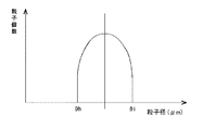
【解決手段】異方性導電フィルムの製造方法は、複数の開口部を有する部材10上に、複数の粒子径の導電粒子20a〜20cを供給し、開口部に導電粒子を保持させる保持工程と、開口部に保持された導電粒子を接着フィルムに転写する転写工程とを有し、開口部に保持された導電粒子の粒子径分布グラフ(X軸:粒子径[μm]、Y軸:粒子個数)において、最大ピークの粒子径以上の範囲で傾きが実質的に無限大となるグラフ形状となる。
【選択図】図1
Description
1.異方性導電フィルムの製造方法
2.異方性導電フィルム
3.接続構造体の製造方法、及び接続構造体
4.フィラー配置フィルムの製造方法、及びフィラー配置フィルム
5.実施例
本実施の形態に係る異方性導電フィルムの製造方法は、複数の開口部を有する部材上に、複数の粒子径の導電粒子を供給し、開口部に導電粒子を保持させる保持工程(A)と、開口部に保持された導電粒子を接着フィルムに転写する転写工程(B)とを有する。以下、保持工程(A)、及び転写工程(B)について説明する。
[保持工程(A)]
図1は、複数の開口部を有する部材上に導電粒子が供給された状態を模式的に示す断面図である。図1に示すように、部材10は、所定の開口径又は開口幅の開口サイズSを有する開口部を有する型である。型としては、例えば、ステンレスなどの金属材料、ガラスなどの透明無機材料、ポリ(メタ)アクリレートや結晶性樹脂等の有機材料が挙げられる。開口形成方法は種々公知の技術によって形成させることができる。例えば機械加工によって設けてもよく、フォトリソグラフィを利用してもよく、印刷法を利用してもよく、特に限定はない。また、型は、板状、ロール状等種々の形状をとることができ、特に制限はされない。
導電粒子としては、公知の異方性導電フィルムにおいて使用されているものを適宜選択して使用することができる。例えば、ニッケル、銅、銀、金、パラジウムなどの金属粒子、ポリアミド、ポリベンゾグアナミン等の樹脂粒子の表面をニッケルなどの金属で被覆した金属被覆樹脂粒子等を挙げることができる。配置される導電粒子の大きさは、一例として0.5〜50μmであることが好ましく、1〜30μmがより好ましい。
K=(3/√2)F・S-8/2・R-1/2 (1)
(式中、F:導電粒子の20%圧縮変形時における荷重
S:圧縮変位(mm)
R:導電粒子の半径(mm) )
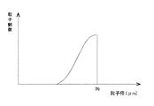
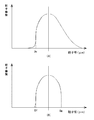
図2(A)は、開口部に供給される導電粒子の粒子径分布を模式的に示すグラフであり、図2(B)は、開口部に保持される導電粒子の粒子径分布を模式的に示すグラフである。この粒子径分布グラフは、光学顕微鏡や金属顕微鏡の面視野観察で1000個以上、好ましくは5000個以上の導電粒子の最大長(粒子径)を測定した個数分布である。図2(A)に示すように、本法は、開口部に供給される導電粒子の粒子径分布が広くても(ブロードでも)よいことから、粒子径の下限側を分級したものを使用するなど、性能とコストのバランスを取り易くなる効果が期待でき、利用可能性の選択肢が増えるという利点がある。
次の転写工程(B)では、先ず、図8に示すように、開口が形成された部材10表面に接着フィルム30を対向させる。
本実施の形態に係る異方性導電フィルムは、フィルム状に形成された絶縁性バインダーと、絶縁性バインダーに面視野で配置される複数の導電粒子とを備え、導電粒子の粒子径分布グラフ(X軸:粒子径[μm]、Y軸:粒子個数)において、最大ピークの粒子径以上の範囲で傾きが実質的に無限大となるグラフ形状となるものである。X軸の粒子径は、1〜30μmの範囲であることが好ましい。この粒子径分布グラフは、光学顕微鏡や金属顕微鏡の面視野観察で1000個以上、好ましくは5000個以上の導電粒子の最大長(粒子径)を測定した個数分布である。
前述した異方性導電フィルムは、電子部品の接続を連続して行うため、ロールに巻かれたフィルム巻装体であることが好ましい。フィルム巻装体の長さは、5m以上であればよく、10m以上であることが好ましい。上限は特にないが、出荷物の取り扱い性の点から、5000m以下であることが好ましく、1000m以下であることがより好ましく、500m以下であることがさらに好ましい。
本技術に係る接続構造体の製造方法は、フィルム状に形成された絶縁性バインダーと、絶縁性バインダーに面視野で配置される複数の導電粒子とを備え、導電粒子の粒子径分布グラフ(X軸:粒子径[μm]、Y軸:粒子個数)において、最大ピークの粒子径以上の範囲で傾きが実質的に無限大となるグラフ形状となる異方性導電フィルムを介して第1の電子部品と第2の電子部品とを配置する配置工程(S1)と、圧着ツールにより第2の電子部品を第1の電子部品に圧着させるとともに、異方性導電フィルムを硬化させる硬化工程(S2)とを有する。
図9(A)に示すように、配置工程(S1)では、フィルム状に形成された絶縁性バインダーと、絶縁性バインダーに面視野で配置される複数の導電粒子とを備え、導電粒子の粒子径分布グラフ(X軸:粒子径[μm]、Y軸:粒子個数)において、最大ピークの粒子径以上の範囲で傾きが実質的に無限大となるグラフ形状となる異方性導電フィルム60を介して第1の電子部品50と第2の電子部品70とを配置する。
図9(B)に示すように、硬化工程(S2)では、圧着ツール80により第2の電子部品70を第1の電子部品50に圧着させる。これにより、圧着ツール80により第2の電子部品が十分に押し込まれ、導電粒子61が端子間に挟持された状態で樹脂が硬化する。
上述した異方性導電フィルムの製造方法は、導電粒子に代えて導電粒子と同様なフィラーを使用することにより、フィラーが面視野で配置されるフィラー配置フィルムを製造することができる。
以下、本技術の実施例について説明する。本実施例では、所定の比率(個数換算)で混合された導電粒子を、開口配列パターンが形成された樹脂型に供給して開口に導電粒子を保持させ、開口に保持された導電粒子を接着フィルムに転写することにより異方性導電フィルムを作製した。そして、異方性導電フィルムの分級評価を行った。また、異方性導電フィルムを用いて接続構造体を作製し、接続構造体の導通性評価、補足性評価、及びショート評価を行った。なお、本技術は、これらの実施例に限定されるものではない。例えば、導電粒子に代えて樹脂粒子を使用したフィラー配置フィルムの製造方法およびフィラー配置フィルムの実施例についても、異方性導電フィルムの分級評価の結果と同様の効果が得られる。
(樹脂型の作製)
3μmの導電粒子が平面視において正方格子配列で格子軸と異方性導電フィルムの短手方向とのなす角度θが15°となり、粒子間距離が導電粒子の粒子径の2倍と等しくなり、導電粒子の個数密度が28000個/mm2となるように、上記配列パターンに則った凸部を有する金型を作製した。金型の凸部は3.3μm×3.3μmの正方形であり、この中心点におけるピッチが平均導電粒子径3μmの2倍となる6μmとした。また、凸部の高さ(即ち、開口の深さ)は3.5μmとした。この金型に、公知の透明性樹脂のペレットを溶融させた状態で流し込み、冷やして固めることで、開口配列パターンが形成された樹脂型を形成した。得られた樹脂型の開口の深さは凸部の高さとほぼ同じであった。
下記配合の樹脂組成物Aをバーコーターでフィルム厚さ50μmのPETフィルム上に塗布し、80℃のオーブンにて5分間乾燥させ、PETフィルム上に厚さ4μmの絶縁性樹脂層Aを形成した。
フェノキシ樹脂(YP−50、新日鉄住金化学(株)):30質量部、エポキシ樹脂(jER828、三菱化学(株)):40質量部、カチオン硬化剤(SI−60L、三新化学工業(株)):2質量部、フィラー(アエロジルRX300、日本アエロジル(株)):30質量部
フェノキシ樹脂(YP−50、新日鉄住金化学(株)):30質量部、フェノキシ樹脂(FX−316ATM55、新日鉄住金化学(株)):30質量部、エポキシ樹脂(jER828、三菱化学(株)):40質量部、カチオン硬化剤(SI−60L、三新化学工業(株)):2質量部
導電粒子として、3μmの金属被覆樹脂粒子(積水化学工業(株)、AUL703、平均粒子径3μm、以下「3μm径粒子」と記す)と、5μmの金属被覆樹脂粒子(積水化学工業(株)、AUL705、平均粒子径5μm、以下「5μm径粒子」と記す)とを準備した。
異方性導電フィルムA〜Eの導電粒子含有層のフィルム面を金属顕微鏡により観察することで、配列における粒子抜けを評価した。異方性導電フィルムA〜Eの観察は、フィルム長手方向に50μm、フィルム幅方向に200μmの面積を、連続しない10箇所で行い、これを5箇所で繰り返し、合計5mm2の面積を行った。
異方性導電フィルムA〜Eを導通性評価用ICとガラス基板との間に挟み、加熱加圧(180℃、60MPa、5秒)して導通性評価用の接続構造体を作製した。そして、各接続構造体の導通抵抗を、接続後の初期、及び、温度85℃、湿度85%RHの恒温槽に500時間静置した信頼性試験後に測定した。
外形 1.8×20.0mm
厚み 0.5mm
バンプ仕様 サイズ30×85μm、バンプ間距離50μm、バンプ高さ15μm
ガラス基板(ITO配線):
ガラス材質 コーニング社製1737F
外径 30×50mm
厚み 0.5mm
電極 ITO配線
導通性評価用の接続構造体を用いて、導電粒子の捕捉状態について圧痕検査を行った。その結果、異方性導電フィルムA〜Eの全てにおいて、バンプ1個当たり少なくとも3個以上の導電粒子が、各々独立した圧痕となっていることが確認できた。また、捕捉数については、3μm径粒子の混合比率が高いほど補足数が多い傾向となり、3μm径のみを使用した異方性導電フィルムEが最も捕捉数が多かった。
導通性評価用の各接続構造体について、バンプ間100個においてショートしているチャンネル数を計測し、ショート数とした。その結果、異方性導電フィルムA〜Eを用いた接続構造体の全てにおいて、ショートしているものはなかった。
外形 1.5×13mm
厚み 0.5mm
バンプ仕様 金メッキ、高さ15μm、サイズ25×140μm、バンプ間距離7.5μm
異方性導電フィルムの分級評価、接続構造体の導通性評価、補足性評価、及びショート評価のいずれにおいても、本技術を適用させた異方性導電フィルムA〜Dは、3μm径粒子のみを使用した異方性導電フィルムEと同等であり、実用上問題ないことが分かった。すなわち、本技術を適用することにより、粒子径分布がブロードな導電粒子を使用することができ、製造コストを削減することができる。また、異方性導電フィルムの分級評価の結果から、フィラー配置フィルムでも同様の効果が得られることが分かる。
Claims (11)
- 複数の開口部を有する部材上に、複数の粒子径の導電粒子を供給し、前記開口部に導電粒子を保持させる保持工程と、前記開口部に保持された導電粒子を接着フィルムに転写する転写工程とを有し、
前記開口部に保持された導電粒子の粒子径分布グラフ(X軸:粒子径[μm]、Y軸:粒子個数)において、最大ピークの粒子径以上の範囲で傾きが実質的に無限大となるグラフ形状となる異方性導電フィルムの製造方法。 - 前記保持工程にて供給される導電粒子の粒子径分布グラフ(X軸:粒子径[μm]、Y軸:粒子個数)において、最大ピークの粒子径以下の範囲で傾きが実質的に無限大となる粒子径を有する請求項1記載の異方性導電フィルムの製造方法。
- 前記保持工程において供給される複数の導電粒子の表面が、絶縁体によって被覆されている請求項1又は2記載の異方性導電フィルムの製造方法。
- フィルム状に形成された絶縁性バインダーと、
前記絶縁性バインダーに面視野で配置される複数の導電粒子とを備え、
前記導電粒子の粒子径分布グラフ(X軸:粒子径[μm]、Y軸:粒子個数)において、最大ピークの粒子径以上の範囲で傾きが実質的に無限大となるグラフ形状となる異方性導電フィルム。 - 導電粒子の粒子径分布グラフ(X軸:粒子径[μm]、Y軸:粒子個数)において、最大ピークの粒子径以下の範囲で傾きが実質的に無限大となる粒子径を有する請求項4記載の異方性導電フィルム。
- 導電粒子の粒子径分布グラフ(X軸:粒子径[μm]、Y軸:粒子個数)において、複数のピークを有するグラフ形状となる請求項4又は5記載の異方性導電フィルム。
- 前記請求項4〜6のいずれか1項に記載の異方性導電フィルムが巻き芯に巻かれている異方性導電フィルム巻装体。
- フィルム状に形成された絶縁性バインダーと、前記絶縁性バインダーに面視野で配置される複数の導電粒子とを備え、前記導電粒子の粒子径分布グラフ(X軸:粒子径[μm]、Y軸:粒子個数)において、最大ピークの粒子径以上の範囲で傾きが実質的に無限大となるグラフ形状となる異方性導電フィルムを介して第1の電子部品と第2の電子部品とを配置する配置工程と、
圧着ツールにより前記第2の電子部品を前記第1の電子部品に圧着させるとともに、前記異方性導電フィルムを硬化させる硬化工程と
を有する接続構造体の製造方法。 - 第1の電子部品と、第2の電子部品と、前記第1の電子部品と前記第2の電子部品とが接着された接着膜とを備え、
前記接着膜は、フィルム状に形成された絶縁性バインダーと、前記絶縁性バインダーに面視野で配置される複数の導電粒子とを備え、前記導電粒子の粒子径分布グラフ(X軸:粒子径[μm]、Y軸:粒子個数)において、最大ピークの粒子径以上の範囲で傾きが実質的に無限大となるグラフ形状となる異方性導電フィルムが硬化してなる接続構造体。 - 複数の開口部を有する部材上に、複数の粒子径のフィラーを供給し、前記開口部にフィラーを保持させる保持工程と、前記開口部に保持されたフィラーを接着フィルムに転写する転写工程とを有し、
前記開口部に保持されたフィラーの粒子径分布グラフ(X軸:粒子径[μm]、Y軸:粒子個数)において、最大ピークの粒子径以上の範囲で傾きが実質的に無限大となるグラフ形状となるフィラー配置フィルムの製造方法。 - フィルム状に形成された絶縁性バインダーと、
前記絶縁性バインダーに面視野で配置される複数のフィラーとを備え、
前記フィラーの粒子径分布グラフ(X軸:粒子径[μm]、Y軸:粒子個数)において、最大ピークの粒子径以上の範囲で傾きが実質的に無限大となるグラフ形状となるフィラー配置フィルム。
Priority Applications (9)
| Application Number | Priority Date | Filing Date | Title |
|---|---|---|---|
| KR1020217012297A KR102445646B1 (ko) | 2016-05-02 | 2017-04-25 | 이방성 도전 필름의 제조 방법 및 이방성 도전 필름 |
| CN201780020535.7A CN108886227B (zh) | 2016-05-02 | 2017-04-25 | 各向异性导电膜的制造方法及各向异性导电膜 |
| KR1020187029867A KR102246259B1 (ko) | 2016-05-02 | 2017-04-25 | 이방성 도전 필름의 제조 방법 및 이방성 도전 필름 |
| PCT/JP2017/016255 WO2017191776A1 (ja) | 2016-05-02 | 2017-04-25 | 異方性導電フィルムの製造方法、及び異方性導電フィルム |
| US16/087,526 US11004574B2 (en) | 2016-05-02 | 2017-04-25 | Method for manufacturing anisotropic conductive film, and anisotropic conductive film |
| TW110129669A TWI775562B (zh) | 2016-05-02 | 2017-05-01 | 異向性導電膜之製造方法、異向性導電膜、異向性導電膜捲裝體、連接構造體之製造方法、連接構造體、填料配置膜之製造方法、及填料配置膜 |
| TW106114397A TWI738772B (zh) | 2016-05-02 | 2017-05-01 | 異向性導電膜之製造方法,及異向性導電膜 |
| US17/315,862 US20210265076A1 (en) | 2016-05-02 | 2021-05-10 | Method for manufacturing anisotropic conductive film, and anisotropic conductive film |
| JP2021085711A JP7194229B2 (ja) | 2016-05-02 | 2021-05-20 | 異方性導電フィルムの製造方法、及び異方性導電フィルム |
Applications Claiming Priority (2)
| Application Number | Priority Date | Filing Date | Title |
|---|---|---|---|
| JP2016092832 | 2016-05-02 | ||
| JP2016092832 | 2016-05-02 |
Related Child Applications (1)
| Application Number | Title | Priority Date | Filing Date |
|---|---|---|---|
| JP2021085711A Division JP7194229B2 (ja) | 2016-05-02 | 2021-05-20 | 異方性導電フィルムの製造方法、及び異方性導電フィルム |
Publications (3)
| Publication Number | Publication Date |
|---|---|
| JP2017201624A true JP2017201624A (ja) | 2017-11-09 |
| JP2017201624A5 JP2017201624A5 (ja) | 2020-08-20 |
| JP6889020B2 JP6889020B2 (ja) | 2021-06-18 |
Family
ID=60264744
Family Applications (2)
| Application Number | Title | Priority Date | Filing Date |
|---|---|---|---|
| JP2017085492A Active JP6889020B2 (ja) | 2016-05-02 | 2017-04-24 | 異方性導電フィルムの製造方法、及び異方性導電フィルム |
| JP2021085711A Active JP7194229B2 (ja) | 2016-05-02 | 2021-05-20 | 異方性導電フィルムの製造方法、及び異方性導電フィルム |
Family Applications After (1)
| Application Number | Title | Priority Date | Filing Date |
|---|---|---|---|
| JP2021085711A Active JP7194229B2 (ja) | 2016-05-02 | 2021-05-20 | 異方性導電フィルムの製造方法、及び異方性導電フィルム |
Country Status (5)
| Country | Link |
|---|---|
| US (2) | US11004574B2 (ja) |
| JP (2) | JP6889020B2 (ja) |
| KR (1) | KR102246259B1 (ja) |
| CN (1) | CN108886227B (ja) |
| TW (1) | TWI738772B (ja) |
Citations (10)
| Publication number | Priority date | Publication date | Assignee | Title |
|---|---|---|---|---|
| US20030155656A1 (en) * | 2002-01-18 | 2003-08-21 | Chiu Cindy Chia-Wen | Anisotropically conductive film |
| JP2007216213A (ja) * | 2006-01-17 | 2007-08-30 | Powdertech Co Ltd | 造粒方法、造粒物及び造粒装置 |
| JP2007297636A (ja) * | 2007-06-14 | 2007-11-15 | Nippon Zeon Co Ltd | 異方性導電用樹脂組成物 |
| JP2008300360A (ja) * | 1995-02-07 | 2008-12-11 | Hitachi Chem Co Ltd | 電極の接続方法 |
| JP2010176910A (ja) * | 2009-01-27 | 2010-08-12 | Panasonic Electric Works Co Ltd | 導電性シート材料及び電気的接続構造 |
| WO2013005831A1 (ja) * | 2011-07-07 | 2013-01-10 | 日立化成工業株式会社 | 回路接続材料及び回路基板の接続構造体 |
| JP2013055045A (ja) * | 2011-08-05 | 2013-03-21 | Sekisui Chem Co Ltd | 接続構造体の製造方法、接続構造体及び異方性導電材料 |
| JP2013258136A (ja) * | 2012-05-14 | 2013-12-26 | Sekisui Chem Co Ltd | 導電性粒子材料、導電材料、接続構造体及び接続構造体の製造方法 |
| JP2014060151A (ja) * | 2012-08-24 | 2014-04-03 | Dexerials Corp | 異方性導電フィルムの製造方法及び異方性導電フィルム |
| JP2015135748A (ja) * | 2014-01-17 | 2015-07-27 | デクセリアルズ株式会社 | 異方性導電フィルム、接続構造体、接続構造体の製造方法、及び接続構造体の製造装置 |
Family Cites Families (19)
| Publication number | Priority date | Publication date | Assignee | Title |
|---|---|---|---|---|
| JP2737647B2 (ja) * | 1994-03-10 | 1998-04-08 | カシオ計算機株式会社 | 異方導電性接着剤およびそれを用いた導電接続構造 |
| JP4016491B2 (ja) | 1998-07-29 | 2007-12-05 | 凸版印刷株式会社 | スキージとスキージング機構およびそれを用いたスクリーン印刷方法 |
| JP2004223788A (ja) | 2003-01-21 | 2004-08-12 | Yamaha Motor Co Ltd | スキージ及びスクリーン印刷機 |
| KR100591074B1 (ko) * | 2004-12-13 | 2006-06-19 | (주) 선양디엔티 | 칩 온 필름용 이방성 도전물 부착 시스템 |
| JP4890053B2 (ja) * | 2006-03-02 | 2012-03-07 | 旭化成イーマテリアルズ株式会社 | 微細回路検査用異方導電性フィルム |
| JP2010033793A (ja) | 2008-07-28 | 2010-02-12 | Tokai Rubber Ind Ltd | 粒子転写膜の製造方法 |
| JP5755527B2 (ja) * | 2011-08-09 | 2015-07-29 | 木村 潔 | 異方導電性膜および導電性コネクタ |
| JP2013182823A (ja) * | 2012-03-02 | 2013-09-12 | Dexerials Corp | 接続体の製造方法、及び異方性導電接着剤 |
| JP5706998B2 (ja) * | 2012-04-26 | 2015-04-22 | 国立大学法人大阪大学 | 透明導電性インク及び透明導電パターン形成方法 |
| CN109166649B (zh) * | 2012-08-24 | 2021-04-13 | 迪睿合电子材料有限公司 | 各向异性导电膜及其制造方法 |
| US10412837B2 (en) * | 2012-08-29 | 2019-09-10 | Dexerials Corporation | Anisotropic conductive film and method of producing the same |
| JP5964187B2 (ja) | 2012-09-18 | 2016-08-03 | デクセリアルズ株式会社 | 異方性導電フィルム、接続方法、及び接合体 |
| JP6133069B2 (ja) * | 2013-01-30 | 2017-05-24 | デクセリアルズ株式会社 | 加熱硬化型接着フィルム |
| JP2015034279A (ja) | 2013-04-10 | 2015-02-19 | デクセリアルズ株式会社 | 透明導電膜形成用インク組成物、透明導電膜、透明電極の製造方法、及び画像表示装置 |
| CN105359342B (zh) * | 2013-07-31 | 2018-02-23 | 迪睿合株式会社 | 各向异性导电膜及其制造方法 |
| WO2015029881A1 (ja) * | 2013-08-30 | 2015-03-05 | 富士フイルム株式会社 | 金属充填微細構造体の製造方法 |
| WO2015068654A1 (ja) | 2013-11-05 | 2015-05-14 | 昭和電工株式会社 | 導電パターン形成方法及びこれを使用したオンセル型タッチパネルの製造方法並びにこれに使用する転写用フィルム及びオンセル型タッチパネル |
| JP6241326B2 (ja) * | 2014-03-07 | 2017-12-06 | デクセリアルズ株式会社 | 異方性導電フィルム及びその製造方法 |
| WO2015151874A1 (ja) * | 2014-03-31 | 2015-10-08 | デクセリアルズ株式会社 | 異方性導電フィルム及びその製造方法 |
-
2017
- 2017-04-24 JP JP2017085492A patent/JP6889020B2/ja active Active
- 2017-04-25 US US16/087,526 patent/US11004574B2/en active Active
- 2017-04-25 KR KR1020187029867A patent/KR102246259B1/ko active IP Right Grant
- 2017-04-25 CN CN201780020535.7A patent/CN108886227B/zh active Active
- 2017-05-01 TW TW106114397A patent/TWI738772B/zh active
-
2021
- 2021-05-10 US US17/315,862 patent/US20210265076A1/en active Pending
- 2021-05-20 JP JP2021085711A patent/JP7194229B2/ja active Active
Patent Citations (10)
| Publication number | Priority date | Publication date | Assignee | Title |
|---|---|---|---|---|
| JP2008300360A (ja) * | 1995-02-07 | 2008-12-11 | Hitachi Chem Co Ltd | 電極の接続方法 |
| US20030155656A1 (en) * | 2002-01-18 | 2003-08-21 | Chiu Cindy Chia-Wen | Anisotropically conductive film |
| JP2007216213A (ja) * | 2006-01-17 | 2007-08-30 | Powdertech Co Ltd | 造粒方法、造粒物及び造粒装置 |
| JP2007297636A (ja) * | 2007-06-14 | 2007-11-15 | Nippon Zeon Co Ltd | 異方性導電用樹脂組成物 |
| JP2010176910A (ja) * | 2009-01-27 | 2010-08-12 | Panasonic Electric Works Co Ltd | 導電性シート材料及び電気的接続構造 |
| WO2013005831A1 (ja) * | 2011-07-07 | 2013-01-10 | 日立化成工業株式会社 | 回路接続材料及び回路基板の接続構造体 |
| JP2013055045A (ja) * | 2011-08-05 | 2013-03-21 | Sekisui Chem Co Ltd | 接続構造体の製造方法、接続構造体及び異方性導電材料 |
| JP2013258136A (ja) * | 2012-05-14 | 2013-12-26 | Sekisui Chem Co Ltd | 導電性粒子材料、導電材料、接続構造体及び接続構造体の製造方法 |
| JP2014060151A (ja) * | 2012-08-24 | 2014-04-03 | Dexerials Corp | 異方性導電フィルムの製造方法及び異方性導電フィルム |
| JP2015135748A (ja) * | 2014-01-17 | 2015-07-27 | デクセリアルズ株式会社 | 異方性導電フィルム、接続構造体、接続構造体の製造方法、及び接続構造体の製造装置 |
Also Published As
| Publication number | Publication date |
|---|---|
| JP7194229B2 (ja) | 2022-12-21 |
| CN108886227B (zh) | 2021-03-09 |
| JP2021122027A (ja) | 2021-08-26 |
| US20190103201A1 (en) | 2019-04-04 |
| KR102246259B1 (ko) | 2021-04-29 |
| TWI738772B (zh) | 2021-09-11 |
| JP6889020B2 (ja) | 2021-06-18 |
| US11004574B2 (en) | 2021-05-11 |
| US20210265076A1 (en) | 2021-08-26 |
| TW201810302A (zh) | 2018-03-16 |
| KR20180122002A (ko) | 2018-11-09 |
| CN108886227A (zh) | 2018-11-23 |
Similar Documents
| Publication | Publication Date | Title |
|---|---|---|
| US11794444B2 (en) | Anisotropic conductive film | |
| US10899949B2 (en) | Filler-containing film | |
| JP7315878B2 (ja) | フィラー含有フィルム | |
| KR102149964B1 (ko) | 이방성 도전 필름 | |
| US10854571B2 (en) | Anisotropic conductive film with conductive particles forming repeating units of polygons | |
| KR102652055B1 (ko) | 필러 함유 필름 | |
| JP7087305B2 (ja) | フィラー含有フィルム | |
| JP7081097B2 (ja) | フィラー含有フィルム | |
| WO2017191776A1 (ja) | 異方性導電フィルムの製造方法、及び異方性導電フィルム | |
| JP7332956B2 (ja) | フィラー含有フィルム | |
| JP2022126655A (ja) | フィラー含有フィルム | |
| KR20190038603A (ko) | 필러 함유 필름 | |
| JP7194229B2 (ja) | 異方性導電フィルムの製造方法、及び異方性導電フィルム | |
| WO2017191781A1 (ja) | 異方性導電フィルム | |
| JP7319578B2 (ja) | フィラー含有フィルム |
Legal Events
| Date | Code | Title | Description |
|---|---|---|---|
| A621 | Written request for application examination |
Free format text: JAPANESE INTERMEDIATE CODE: A621 Effective date: 20200423 |
|
| A521 | Request for written amendment filed |
Free format text: JAPANESE INTERMEDIATE CODE: A523 Effective date: 20200708 |
|
| TRDD | Decision of grant or rejection written | ||
| A01 | Written decision to grant a patent or to grant a registration (utility model) |
Free format text: JAPANESE INTERMEDIATE CODE: A01 Effective date: 20210420 |
|
| A61 | First payment of annual fees (during grant procedure) |
Free format text: JAPANESE INTERMEDIATE CODE: A61 Effective date: 20210520 |
|
| R150 | Certificate of patent or registration of utility model |
Ref document number: 6889020 Country of ref document: JP Free format text: JAPANESE INTERMEDIATE CODE: R150 |
|
| R250 | Receipt of annual fees |
Free format text: JAPANESE INTERMEDIATE CODE: R250 |