WO2017191776A1 - 異方性導電フィルムの製造方法、及び異方性導電フィルム - Google Patents
異方性導電フィルムの製造方法、及び異方性導電フィルム Download PDFInfo
- Publication number
- WO2017191776A1 WO2017191776A1 PCT/JP2017/016255 JP2017016255W WO2017191776A1 WO 2017191776 A1 WO2017191776 A1 WO 2017191776A1 JP 2017016255 W JP2017016255 W JP 2017016255W WO 2017191776 A1 WO2017191776 A1 WO 2017191776A1
- Authority
- WO
- WIPO (PCT)
- Prior art keywords
- particle size
- conductive particles
- particles
- film
- axis
- Prior art date
Links
Images


Classifications
-
- H—ELECTRICITY
- H01—ELECTRIC ELEMENTS
- H01B—CABLES; CONDUCTORS; INSULATORS; SELECTION OF MATERIALS FOR THEIR CONDUCTIVE, INSULATING OR DIELECTRIC PROPERTIES
- H01B13/00—Apparatus or processes specially adapted for manufacturing conductors or cables
-
- C—CHEMISTRY; METALLURGY
- C08—ORGANIC MACROMOLECULAR COMPOUNDS; THEIR PREPARATION OR CHEMICAL WORKING-UP; COMPOSITIONS BASED THEREON
- C08K—Use of inorganic or non-macromolecular organic substances as compounding ingredients
- C08K9/00—Use of pretreated ingredients
- C08K9/02—Ingredients treated with inorganic substances
-
- H—ELECTRICITY
- H01—ELECTRIC ELEMENTS
- H01B—CABLES; CONDUCTORS; INSULATORS; SELECTION OF MATERIALS FOR THEIR CONDUCTIVE, INSULATING OR DIELECTRIC PROPERTIES
- H01B1/00—Conductors or conductive bodies characterised by the conductive materials; Selection of materials as conductors
- H01B1/20—Conductive material dispersed in non-conductive organic material
- H01B1/22—Conductive material dispersed in non-conductive organic material the conductive material comprising metals or alloys
-
- C—CHEMISTRY; METALLURGY
- C09—DYES; PAINTS; POLISHES; NATURAL RESINS; ADHESIVES; COMPOSITIONS NOT OTHERWISE PROVIDED FOR; APPLICATIONS OF MATERIALS NOT OTHERWISE PROVIDED FOR
- C09J—ADHESIVES; NON-MECHANICAL ASPECTS OF ADHESIVE PROCESSES IN GENERAL; ADHESIVE PROCESSES NOT PROVIDED FOR ELSEWHERE; USE OF MATERIALS AS ADHESIVES
- C09J7/00—Adhesives in the form of films or foils
- C09J7/30—Adhesives in the form of films or foils characterised by the adhesive composition
-
- C—CHEMISTRY; METALLURGY
- C09—DYES; PAINTS; POLISHES; NATURAL RESINS; ADHESIVES; COMPOSITIONS NOT OTHERWISE PROVIDED FOR; APPLICATIONS OF MATERIALS NOT OTHERWISE PROVIDED FOR
- C09J—ADHESIVES; NON-MECHANICAL ASPECTS OF ADHESIVE PROCESSES IN GENERAL; ADHESIVE PROCESSES NOT PROVIDED FOR ELSEWHERE; USE OF MATERIALS AS ADHESIVES
- C09J9/00—Adhesives characterised by their physical nature or the effects produced, e.g. glue sticks
- C09J9/02—Electrically-conducting adhesives
-
- H—ELECTRICITY
- H01—ELECTRIC ELEMENTS
- H01B—CABLES; CONDUCTORS; INSULATORS; SELECTION OF MATERIALS FOR THEIR CONDUCTIVE, INSULATING OR DIELECTRIC PROPERTIES
- H01B13/00—Apparatus or processes specially adapted for manufacturing conductors or cables
- H01B13/34—Apparatus or processes specially adapted for manufacturing conductors or cables for marking conductors or cables
-
- H—ELECTRICITY
- H01—ELECTRIC ELEMENTS
- H01B—CABLES; CONDUCTORS; INSULATORS; SELECTION OF MATERIALS FOR THEIR CONDUCTIVE, INSULATING OR DIELECTRIC PROPERTIES
- H01B5/00—Non-insulated conductors or conductive bodies characterised by their form
- H01B5/16—Non-insulated conductors or conductive bodies characterised by their form comprising conductive material in insulating or poorly conductive material, e.g. conductive rubber
-
- H—ELECTRICITY
- H01—ELECTRIC ELEMENTS
- H01L—SEMICONDUCTOR DEVICES NOT COVERED BY CLASS H10
- H01L24/00—Arrangements for connecting or disconnecting semiconductor or solid-state bodies; Methods or apparatus related thereto
- H01L24/01—Means for bonding being attached to, or being formed on, the surface to be connected, e.g. chip-to-package, die-attach, "first-level" interconnects; Manufacturing methods related thereto
- H01L24/26—Layer connectors, e.g. plate connectors, solder or adhesive layers; Manufacturing methods related thereto
- H01L24/27—Manufacturing methods
-
- H—ELECTRICITY
- H01—ELECTRIC ELEMENTS
- H01L—SEMICONDUCTOR DEVICES NOT COVERED BY CLASS H10
- H01L24/00—Arrangements for connecting or disconnecting semiconductor or solid-state bodies; Methods or apparatus related thereto
- H01L24/01—Means for bonding being attached to, or being formed on, the surface to be connected, e.g. chip-to-package, die-attach, "first-level" interconnects; Manufacturing methods related thereto
- H01L24/26—Layer connectors, e.g. plate connectors, solder or adhesive layers; Manufacturing methods related thereto
- H01L24/28—Structure, shape, material or disposition of the layer connectors prior to the connecting process
- H01L24/29—Structure, shape, material or disposition of the layer connectors prior to the connecting process of an individual layer connector
-
- H—ELECTRICITY
- H01—ELECTRIC ELEMENTS
- H01L—SEMICONDUCTOR DEVICES NOT COVERED BY CLASS H10
- H01L24/00—Arrangements for connecting or disconnecting semiconductor or solid-state bodies; Methods or apparatus related thereto
- H01L24/80—Methods for connecting semiconductor or other solid state bodies using means for bonding being attached to, or being formed on, the surface to be connected
- H01L24/83—Methods for connecting semiconductor or other solid state bodies using means for bonding being attached to, or being formed on, the surface to be connected using a layer connector
-
- H—ELECTRICITY
- H01—ELECTRIC ELEMENTS
- H01R—ELECTRICALLY-CONDUCTIVE CONNECTIONS; STRUCTURAL ASSOCIATIONS OF A PLURALITY OF MUTUALLY-INSULATED ELECTRICAL CONNECTING ELEMENTS; COUPLING DEVICES; CURRENT COLLECTORS
- H01R11/00—Individual connecting elements providing two or more spaced connecting locations for conductive members which are, or may be, thereby interconnected, e.g. end pieces for wires or cables supported by the wire or cable and having means for facilitating electrical connection to some other wire, terminal, or conductive member, blocks of binding posts
- H01R11/01—Individual connecting elements providing two or more spaced connecting locations for conductive members which are, or may be, thereby interconnected, e.g. end pieces for wires or cables supported by the wire or cable and having means for facilitating electrical connection to some other wire, terminal, or conductive member, blocks of binding posts characterised by the form or arrangement of the conductive interconnection between the connecting locations
-
- H—ELECTRICITY
- H01—ELECTRIC ELEMENTS
- H01R—ELECTRICALLY-CONDUCTIVE CONNECTIONS; STRUCTURAL ASSOCIATIONS OF A PLURALITY OF MUTUALLY-INSULATED ELECTRICAL CONNECTING ELEMENTS; COUPLING DEVICES; CURRENT COLLECTORS
- H01R4/00—Electrically-conductive connections between two or more conductive members in direct contact, i.e. touching one another; Means for effecting or maintaining such contact; Electrically-conductive connections having two or more spaced connecting locations for conductors and using contact members penetrating insulation
- H01R4/04—Electrically-conductive connections between two or more conductive members in direct contact, i.e. touching one another; Means for effecting or maintaining such contact; Electrically-conductive connections having two or more spaced connecting locations for conductors and using contact members penetrating insulation using electrically conductive adhesives
-
- H—ELECTRICITY
- H01—ELECTRIC ELEMENTS
- H01R—ELECTRICALLY-CONDUCTIVE CONNECTIONS; STRUCTURAL ASSOCIATIONS OF A PLURALITY OF MUTUALLY-INSULATED ELECTRICAL CONNECTING ELEMENTS; COUPLING DEVICES; CURRENT COLLECTORS
- H01R43/00—Apparatus or processes specially adapted for manufacturing, assembling, maintaining, or repairing of line connectors or current collectors or for joining electric conductors
-
- C—CHEMISTRY; METALLURGY
- C08—ORGANIC MACROMOLECULAR COMPOUNDS; THEIR PREPARATION OR CHEMICAL WORKING-UP; COMPOSITIONS BASED THEREON
- C08K—Use of inorganic or non-macromolecular organic substances as compounding ingredients
- C08K3/00—Use of inorganic substances as compounding ingredients
- C08K3/02—Elements
- C08K3/08—Metals
- C08K2003/0806—Silver
-
- C—CHEMISTRY; METALLURGY
- C08—ORGANIC MACROMOLECULAR COMPOUNDS; THEIR PREPARATION OR CHEMICAL WORKING-UP; COMPOSITIONS BASED THEREON
- C08K—Use of inorganic or non-macromolecular organic substances as compounding ingredients
- C08K3/00—Use of inorganic substances as compounding ingredients
- C08K3/02—Elements
- C08K3/08—Metals
- C08K2003/0831—Gold
-
- C—CHEMISTRY; METALLURGY
- C08—ORGANIC MACROMOLECULAR COMPOUNDS; THEIR PREPARATION OR CHEMICAL WORKING-UP; COMPOSITIONS BASED THEREON
- C08K—Use of inorganic or non-macromolecular organic substances as compounding ingredients
- C08K3/00—Use of inorganic substances as compounding ingredients
- C08K3/02—Elements
- C08K3/08—Metals
- C08K2003/085—Copper
-
- C—CHEMISTRY; METALLURGY
- C08—ORGANIC MACROMOLECULAR COMPOUNDS; THEIR PREPARATION OR CHEMICAL WORKING-UP; COMPOSITIONS BASED THEREON
- C08K—Use of inorganic or non-macromolecular organic substances as compounding ingredients
- C08K3/00—Use of inorganic substances as compounding ingredients
- C08K3/02—Elements
- C08K3/08—Metals
- C08K2003/0862—Nickel
-
- C—CHEMISTRY; METALLURGY
- C08—ORGANIC MACROMOLECULAR COMPOUNDS; THEIR PREPARATION OR CHEMICAL WORKING-UP; COMPOSITIONS BASED THEREON
- C08K—Use of inorganic or non-macromolecular organic substances as compounding ingredients
- C08K2201/00—Specific properties of additives
- C08K2201/001—Conductive additives
-
- C—CHEMISTRY; METALLURGY
- C09—DYES; PAINTS; POLISHES; NATURAL RESINS; ADHESIVES; COMPOSITIONS NOT OTHERWISE PROVIDED FOR; APPLICATIONS OF MATERIALS NOT OTHERWISE PROVIDED FOR
- C09J—ADHESIVES; NON-MECHANICAL ASPECTS OF ADHESIVE PROCESSES IN GENERAL; ADHESIVE PROCESSES NOT PROVIDED FOR ELSEWHERE; USE OF MATERIALS AS ADHESIVES
- C09J2203/00—Applications of adhesives in processes or use of adhesives in the form of films or foils
- C09J2203/326—Applications of adhesives in processes or use of adhesives in the form of films or foils for bonding electronic components such as wafers, chips or semiconductors
-
- C—CHEMISTRY; METALLURGY
- C09—DYES; PAINTS; POLISHES; NATURAL RESINS; ADHESIVES; COMPOSITIONS NOT OTHERWISE PROVIDED FOR; APPLICATIONS OF MATERIALS NOT OTHERWISE PROVIDED FOR
- C09J—ADHESIVES; NON-MECHANICAL ASPECTS OF ADHESIVE PROCESSES IN GENERAL; ADHESIVE PROCESSES NOT PROVIDED FOR ELSEWHERE; USE OF MATERIALS AS ADHESIVES
- C09J2301/00—Additional features of adhesives in the form of films or foils
- C09J2301/30—Additional features of adhesives in the form of films or foils characterized by the chemical, physicochemical or physical properties of the adhesive or the carrier
- C09J2301/314—Additional features of adhesives in the form of films or foils characterized by the chemical, physicochemical or physical properties of the adhesive or the carrier the adhesive layer and/or the carrier being conductive
-
- C—CHEMISTRY; METALLURGY
- C09—DYES; PAINTS; POLISHES; NATURAL RESINS; ADHESIVES; COMPOSITIONS NOT OTHERWISE PROVIDED FOR; APPLICATIONS OF MATERIALS NOT OTHERWISE PROVIDED FOR
- C09J—ADHESIVES; NON-MECHANICAL ASPECTS OF ADHESIVE PROCESSES IN GENERAL; ADHESIVE PROCESSES NOT PROVIDED FOR ELSEWHERE; USE OF MATERIALS AS ADHESIVES
- C09J2301/00—Additional features of adhesives in the form of films or foils
- C09J2301/40—Additional features of adhesives in the form of films or foils characterized by the presence of essential components
- C09J2301/408—Additional features of adhesives in the form of films or foils characterized by the presence of essential components additives as essential feature of the adhesive layer
-
- H—ELECTRICITY
- H01—ELECTRIC ELEMENTS
- H01L—SEMICONDUCTOR DEVICES NOT COVERED BY CLASS H10
- H01L2224/00—Indexing scheme for arrangements for connecting or disconnecting semiconductor or solid-state bodies and methods related thereto as covered by H01L24/00
- H01L2224/01—Means for bonding being attached to, or being formed on, the surface to be connected, e.g. chip-to-package, die-attach, "first-level" interconnects; Manufacturing methods related thereto
- H01L2224/10—Bump connectors; Manufacturing methods related thereto
- H01L2224/12—Structure, shape, material or disposition of the bump connectors prior to the connecting process
- H01L2224/13—Structure, shape, material or disposition of the bump connectors prior to the connecting process of an individual bump connector
- H01L2224/13001—Core members of the bump connector
- H01L2224/13099—Material
- H01L2224/131—Material with a principal constituent of the material being a metal or a metalloid, e.g. boron [B], silicon [Si], germanium [Ge], arsenic [As], antimony [Sb], tellurium [Te] and polonium [Po], and alloys thereof
- H01L2224/13138—Material with a principal constituent of the material being a metal or a metalloid, e.g. boron [B], silicon [Si], germanium [Ge], arsenic [As], antimony [Sb], tellurium [Te] and polonium [Po], and alloys thereof the principal constituent melting at a temperature of greater than or equal to 950°C and less than 1550°C
- H01L2224/13144—Gold [Au] as principal constituent
-
- H—ELECTRICITY
- H01—ELECTRIC ELEMENTS
- H01L—SEMICONDUCTOR DEVICES NOT COVERED BY CLASS H10
- H01L2224/00—Indexing scheme for arrangements for connecting or disconnecting semiconductor or solid-state bodies and methods related thereto as covered by H01L24/00
- H01L2224/01—Means for bonding being attached to, or being formed on, the surface to be connected, e.g. chip-to-package, die-attach, "first-level" interconnects; Manufacturing methods related thereto
- H01L2224/26—Layer connectors, e.g. plate connectors, solder or adhesive layers; Manufacturing methods related thereto
- H01L2224/27—Manufacturing methods
- H01L2224/27001—Involving a temporary auxiliary member not forming part of the manufacturing apparatus, e.g. removable or sacrificial coating, film or substrate
- H01L2224/27003—Involving a temporary auxiliary member not forming part of the manufacturing apparatus, e.g. removable or sacrificial coating, film or substrate for holding or transferring the layer preform
-
- H—ELECTRICITY
- H01—ELECTRIC ELEMENTS
- H01L—SEMICONDUCTOR DEVICES NOT COVERED BY CLASS H10
- H01L2224/00—Indexing scheme for arrangements for connecting or disconnecting semiconductor or solid-state bodies and methods related thereto as covered by H01L24/00
- H01L2224/01—Means for bonding being attached to, or being formed on, the surface to be connected, e.g. chip-to-package, die-attach, "first-level" interconnects; Manufacturing methods related thereto
- H01L2224/26—Layer connectors, e.g. plate connectors, solder or adhesive layers; Manufacturing methods related thereto
- H01L2224/27—Manufacturing methods
- H01L2224/27001—Involving a temporary auxiliary member not forming part of the manufacturing apparatus, e.g. removable or sacrificial coating, film or substrate
- H01L2224/27005—Involving a temporary auxiliary member not forming part of the manufacturing apparatus, e.g. removable or sacrificial coating, film or substrate for aligning the layer connector, e.g. marks, spacers
-
- H—ELECTRICITY
- H01—ELECTRIC ELEMENTS
- H01L—SEMICONDUCTOR DEVICES NOT COVERED BY CLASS H10
- H01L2224/00—Indexing scheme for arrangements for connecting or disconnecting semiconductor or solid-state bodies and methods related thereto as covered by H01L24/00
- H01L2224/01—Means for bonding being attached to, or being formed on, the surface to be connected, e.g. chip-to-package, die-attach, "first-level" interconnects; Manufacturing methods related thereto
- H01L2224/26—Layer connectors, e.g. plate connectors, solder or adhesive layers; Manufacturing methods related thereto
- H01L2224/27—Manufacturing methods
- H01L2224/271—Manufacture and pre-treatment of the layer connector preform
-
- H—ELECTRICITY
- H01—ELECTRIC ELEMENTS
- H01L—SEMICONDUCTOR DEVICES NOT COVERED BY CLASS H10
- H01L2224/00—Indexing scheme for arrangements for connecting or disconnecting semiconductor or solid-state bodies and methods related thereto as covered by H01L24/00
- H01L2224/01—Means for bonding being attached to, or being formed on, the surface to be connected, e.g. chip-to-package, die-attach, "first-level" interconnects; Manufacturing methods related thereto
- H01L2224/26—Layer connectors, e.g. plate connectors, solder or adhesive layers; Manufacturing methods related thereto
- H01L2224/28—Structure, shape, material or disposition of the layer connectors prior to the connecting process
- H01L2224/29—Structure, shape, material or disposition of the layer connectors prior to the connecting process of an individual layer connector
- H01L2224/29001—Core members of the layer connector
- H01L2224/29099—Material
- H01L2224/29198—Material with a principal constituent of the material being a combination of two or more materials in the form of a matrix with a filler, i.e. being a hybrid material, e.g. segmented structures, foams
- H01L2224/29199—Material of the matrix
- H01L2224/2929—Material of the matrix with a principal constituent of the material being a polymer, e.g. polyester, phenolic based polymer, epoxy
-
- H—ELECTRICITY
- H01—ELECTRIC ELEMENTS
- H01L—SEMICONDUCTOR DEVICES NOT COVERED BY CLASS H10
- H01L2224/00—Indexing scheme for arrangements for connecting or disconnecting semiconductor or solid-state bodies and methods related thereto as covered by H01L24/00
- H01L2224/01—Means for bonding being attached to, or being formed on, the surface to be connected, e.g. chip-to-package, die-attach, "first-level" interconnects; Manufacturing methods related thereto
- H01L2224/26—Layer connectors, e.g. plate connectors, solder or adhesive layers; Manufacturing methods related thereto
- H01L2224/28—Structure, shape, material or disposition of the layer connectors prior to the connecting process
- H01L2224/29—Structure, shape, material or disposition of the layer connectors prior to the connecting process of an individual layer connector
- H01L2224/29001—Core members of the layer connector
- H01L2224/29099—Material
- H01L2224/29198—Material with a principal constituent of the material being a combination of two or more materials in the form of a matrix with a filler, i.e. being a hybrid material, e.g. segmented structures, foams
- H01L2224/29298—Fillers
- H01L2224/29299—Base material
- H01L2224/293—Base material with a principal constituent of the material being a metal or a metalloid, e.g. boron [B], silicon [Si], germanium [Ge], arsenic [As], antimony [Sb], tellurium [Te] and polonium [Po], and alloys thereof
- H01L2224/29338—Base material with a principal constituent of the material being a metal or a metalloid, e.g. boron [B], silicon [Si], germanium [Ge], arsenic [As], antimony [Sb], tellurium [Te] and polonium [Po], and alloys thereof the principal constituent melting at a temperature of greater than or equal to 950°C and less than 1550°C
- H01L2224/29339—Silver [Ag] as principal constituent
-
- H—ELECTRICITY
- H01—ELECTRIC ELEMENTS
- H01L—SEMICONDUCTOR DEVICES NOT COVERED BY CLASS H10
- H01L2224/00—Indexing scheme for arrangements for connecting or disconnecting semiconductor or solid-state bodies and methods related thereto as covered by H01L24/00
- H01L2224/01—Means for bonding being attached to, or being formed on, the surface to be connected, e.g. chip-to-package, die-attach, "first-level" interconnects; Manufacturing methods related thereto
- H01L2224/26—Layer connectors, e.g. plate connectors, solder or adhesive layers; Manufacturing methods related thereto
- H01L2224/28—Structure, shape, material or disposition of the layer connectors prior to the connecting process
- H01L2224/29—Structure, shape, material or disposition of the layer connectors prior to the connecting process of an individual layer connector
- H01L2224/29001—Core members of the layer connector
- H01L2224/29099—Material
- H01L2224/29198—Material with a principal constituent of the material being a combination of two or more materials in the form of a matrix with a filler, i.e. being a hybrid material, e.g. segmented structures, foams
- H01L2224/29298—Fillers
- H01L2224/29299—Base material
- H01L2224/293—Base material with a principal constituent of the material being a metal or a metalloid, e.g. boron [B], silicon [Si], germanium [Ge], arsenic [As], antimony [Sb], tellurium [Te] and polonium [Po], and alloys thereof
- H01L2224/29338—Base material with a principal constituent of the material being a metal or a metalloid, e.g. boron [B], silicon [Si], germanium [Ge], arsenic [As], antimony [Sb], tellurium [Te] and polonium [Po], and alloys thereof the principal constituent melting at a temperature of greater than or equal to 950°C and less than 1550°C
- H01L2224/29344—Gold [Au] as principal constituent
-
- H—ELECTRICITY
- H01—ELECTRIC ELEMENTS
- H01L—SEMICONDUCTOR DEVICES NOT COVERED BY CLASS H10
- H01L2224/00—Indexing scheme for arrangements for connecting or disconnecting semiconductor or solid-state bodies and methods related thereto as covered by H01L24/00
- H01L2224/01—Means for bonding being attached to, or being formed on, the surface to be connected, e.g. chip-to-package, die-attach, "first-level" interconnects; Manufacturing methods related thereto
- H01L2224/26—Layer connectors, e.g. plate connectors, solder or adhesive layers; Manufacturing methods related thereto
- H01L2224/28—Structure, shape, material or disposition of the layer connectors prior to the connecting process
- H01L2224/29—Structure, shape, material or disposition of the layer connectors prior to the connecting process of an individual layer connector
- H01L2224/29001—Core members of the layer connector
- H01L2224/29099—Material
- H01L2224/29198—Material with a principal constituent of the material being a combination of two or more materials in the form of a matrix with a filler, i.e. being a hybrid material, e.g. segmented structures, foams
- H01L2224/29298—Fillers
- H01L2224/29299—Base material
- H01L2224/293—Base material with a principal constituent of the material being a metal or a metalloid, e.g. boron [B], silicon [Si], germanium [Ge], arsenic [As], antimony [Sb], tellurium [Te] and polonium [Po], and alloys thereof
- H01L2224/29338—Base material with a principal constituent of the material being a metal or a metalloid, e.g. boron [B], silicon [Si], germanium [Ge], arsenic [As], antimony [Sb], tellurium [Te] and polonium [Po], and alloys thereof the principal constituent melting at a temperature of greater than or equal to 950°C and less than 1550°C
- H01L2224/29347—Copper [Cu] as principal constituent
-
- H—ELECTRICITY
- H01—ELECTRIC ELEMENTS
- H01L—SEMICONDUCTOR DEVICES NOT COVERED BY CLASS H10
- H01L2224/00—Indexing scheme for arrangements for connecting or disconnecting semiconductor or solid-state bodies and methods related thereto as covered by H01L24/00
- H01L2224/01—Means for bonding being attached to, or being formed on, the surface to be connected, e.g. chip-to-package, die-attach, "first-level" interconnects; Manufacturing methods related thereto
- H01L2224/26—Layer connectors, e.g. plate connectors, solder or adhesive layers; Manufacturing methods related thereto
- H01L2224/28—Structure, shape, material or disposition of the layer connectors prior to the connecting process
- H01L2224/29—Structure, shape, material or disposition of the layer connectors prior to the connecting process of an individual layer connector
- H01L2224/29001—Core members of the layer connector
- H01L2224/29099—Material
- H01L2224/29198—Material with a principal constituent of the material being a combination of two or more materials in the form of a matrix with a filler, i.e. being a hybrid material, e.g. segmented structures, foams
- H01L2224/29298—Fillers
- H01L2224/29299—Base material
- H01L2224/293—Base material with a principal constituent of the material being a metal or a metalloid, e.g. boron [B], silicon [Si], germanium [Ge], arsenic [As], antimony [Sb], tellurium [Te] and polonium [Po], and alloys thereof
- H01L2224/29338—Base material with a principal constituent of the material being a metal or a metalloid, e.g. boron [B], silicon [Si], germanium [Ge], arsenic [As], antimony [Sb], tellurium [Te] and polonium [Po], and alloys thereof the principal constituent melting at a temperature of greater than or equal to 950°C and less than 1550°C
- H01L2224/29355—Nickel [Ni] as principal constituent
-
- H—ELECTRICITY
- H01—ELECTRIC ELEMENTS
- H01L—SEMICONDUCTOR DEVICES NOT COVERED BY CLASS H10
- H01L2224/00—Indexing scheme for arrangements for connecting or disconnecting semiconductor or solid-state bodies and methods related thereto as covered by H01L24/00
- H01L2224/01—Means for bonding being attached to, or being formed on, the surface to be connected, e.g. chip-to-package, die-attach, "first-level" interconnects; Manufacturing methods related thereto
- H01L2224/26—Layer connectors, e.g. plate connectors, solder or adhesive layers; Manufacturing methods related thereto
- H01L2224/28—Structure, shape, material or disposition of the layer connectors prior to the connecting process
- H01L2224/29—Structure, shape, material or disposition of the layer connectors prior to the connecting process of an individual layer connector
- H01L2224/29001—Core members of the layer connector
- H01L2224/29099—Material
- H01L2224/29198—Material with a principal constituent of the material being a combination of two or more materials in the form of a matrix with a filler, i.e. being a hybrid material, e.g. segmented structures, foams
- H01L2224/29298—Fillers
- H01L2224/29299—Base material
- H01L2224/293—Base material with a principal constituent of the material being a metal or a metalloid, e.g. boron [B], silicon [Si], germanium [Ge], arsenic [As], antimony [Sb], tellurium [Te] and polonium [Po], and alloys thereof
- H01L2224/29363—Base material with a principal constituent of the material being a metal or a metalloid, e.g. boron [B], silicon [Si], germanium [Ge], arsenic [As], antimony [Sb], tellurium [Te] and polonium [Po], and alloys thereof the principal constituent melting at a temperature of greater than 1550°C
- H01L2224/29364—Palladium [Pd] as principal constituent
-
- H—ELECTRICITY
- H01—ELECTRIC ELEMENTS
- H01L—SEMICONDUCTOR DEVICES NOT COVERED BY CLASS H10
- H01L2224/00—Indexing scheme for arrangements for connecting or disconnecting semiconductor or solid-state bodies and methods related thereto as covered by H01L24/00
- H01L2224/01—Means for bonding being attached to, or being formed on, the surface to be connected, e.g. chip-to-package, die-attach, "first-level" interconnects; Manufacturing methods related thereto
- H01L2224/26—Layer connectors, e.g. plate connectors, solder or adhesive layers; Manufacturing methods related thereto
- H01L2224/28—Structure, shape, material or disposition of the layer connectors prior to the connecting process
- H01L2224/29—Structure, shape, material or disposition of the layer connectors prior to the connecting process of an individual layer connector
- H01L2224/29001—Core members of the layer connector
- H01L2224/29099—Material
- H01L2224/29198—Material with a principal constituent of the material being a combination of two or more materials in the form of a matrix with a filler, i.e. being a hybrid material, e.g. segmented structures, foams
- H01L2224/29298—Fillers
- H01L2224/29299—Base material
- H01L2224/29386—Base material with a principal constituent of the material being a non metallic, non metalloid inorganic material
-
- H—ELECTRICITY
- H01—ELECTRIC ELEMENTS
- H01L—SEMICONDUCTOR DEVICES NOT COVERED BY CLASS H10
- H01L2224/00—Indexing scheme for arrangements for connecting or disconnecting semiconductor or solid-state bodies and methods related thereto as covered by H01L24/00
- H01L2224/01—Means for bonding being attached to, or being formed on, the surface to be connected, e.g. chip-to-package, die-attach, "first-level" interconnects; Manufacturing methods related thereto
- H01L2224/26—Layer connectors, e.g. plate connectors, solder or adhesive layers; Manufacturing methods related thereto
- H01L2224/28—Structure, shape, material or disposition of the layer connectors prior to the connecting process
- H01L2224/29—Structure, shape, material or disposition of the layer connectors prior to the connecting process of an individual layer connector
- H01L2224/29001—Core members of the layer connector
- H01L2224/29099—Material
- H01L2224/29198—Material with a principal constituent of the material being a combination of two or more materials in the form of a matrix with a filler, i.e. being a hybrid material, e.g. segmented structures, foams
- H01L2224/29298—Fillers
- H01L2224/29299—Base material
- H01L2224/2939—Base material with a principal constituent of the material being a polymer, e.g. polyester, phenolic based polymer, epoxy
- H01L2224/29391—The principal constituent being an elastomer, e.g. silicones, isoprene, neoprene
-
- H—ELECTRICITY
- H01—ELECTRIC ELEMENTS
- H01L—SEMICONDUCTOR DEVICES NOT COVERED BY CLASS H10
- H01L2224/00—Indexing scheme for arrangements for connecting or disconnecting semiconductor or solid-state bodies and methods related thereto as covered by H01L24/00
- H01L2224/01—Means for bonding being attached to, or being formed on, the surface to be connected, e.g. chip-to-package, die-attach, "first-level" interconnects; Manufacturing methods related thereto
- H01L2224/26—Layer connectors, e.g. plate connectors, solder or adhesive layers; Manufacturing methods related thereto
- H01L2224/28—Structure, shape, material or disposition of the layer connectors prior to the connecting process
- H01L2224/29—Structure, shape, material or disposition of the layer connectors prior to the connecting process of an individual layer connector
- H01L2224/29001—Core members of the layer connector
- H01L2224/29099—Material
- H01L2224/29198—Material with a principal constituent of the material being a combination of two or more materials in the form of a matrix with a filler, i.e. being a hybrid material, e.g. segmented structures, foams
- H01L2224/29298—Fillers
- H01L2224/29399—Coating material
- H01L2224/294—Coating material with a principal constituent of the material being a metal or a metalloid, e.g. boron [B], silicon [Si], germanium [Ge], arsenic [As], antimony [Sb], tellurium [Te] and polonium [Po], and alloys thereof
- H01L2224/29438—Coating material with a principal constituent of the material being a metal or a metalloid, e.g. boron [B], silicon [Si], germanium [Ge], arsenic [As], antimony [Sb], tellurium [Te] and polonium [Po], and alloys thereof the principal constituent melting at a temperature of greater than or equal to 950°C and less than 1550°C
- H01L2224/29455—Nickel [Ni] as principal constituent
-
- H—ELECTRICITY
- H01—ELECTRIC ELEMENTS
- H01L—SEMICONDUCTOR DEVICES NOT COVERED BY CLASS H10
- H01L2224/00—Indexing scheme for arrangements for connecting or disconnecting semiconductor or solid-state bodies and methods related thereto as covered by H01L24/00
- H01L2224/01—Means for bonding being attached to, or being formed on, the surface to be connected, e.g. chip-to-package, die-attach, "first-level" interconnects; Manufacturing methods related thereto
- H01L2224/26—Layer connectors, e.g. plate connectors, solder or adhesive layers; Manufacturing methods related thereto
- H01L2224/28—Structure, shape, material or disposition of the layer connectors prior to the connecting process
- H01L2224/29—Structure, shape, material or disposition of the layer connectors prior to the connecting process of an individual layer connector
- H01L2224/29001—Core members of the layer connector
- H01L2224/29099—Material
- H01L2224/29198—Material with a principal constituent of the material being a combination of two or more materials in the form of a matrix with a filler, i.e. being a hybrid material, e.g. segmented structures, foams
- H01L2224/29298—Fillers
- H01L2224/29499—Shape or distribution of the fillers
-
- H—ELECTRICITY
- H01—ELECTRIC ELEMENTS
- H01L—SEMICONDUCTOR DEVICES NOT COVERED BY CLASS H10
- H01L2224/00—Indexing scheme for arrangements for connecting or disconnecting semiconductor or solid-state bodies and methods related thereto as covered by H01L24/00
- H01L2224/01—Means for bonding being attached to, or being formed on, the surface to be connected, e.g. chip-to-package, die-attach, "first-level" interconnects; Manufacturing methods related thereto
- H01L2224/26—Layer connectors, e.g. plate connectors, solder or adhesive layers; Manufacturing methods related thereto
- H01L2224/31—Structure, shape, material or disposition of the layer connectors after the connecting process
- H01L2224/32—Structure, shape, material or disposition of the layer connectors after the connecting process of an individual layer connector
- H01L2224/321—Disposition
- H01L2224/32151—Disposition the layer connector connecting between a semiconductor or solid-state body and an item not being a semiconductor or solid-state body, e.g. chip-to-substrate, chip-to-passive
- H01L2224/32221—Disposition the layer connector connecting between a semiconductor or solid-state body and an item not being a semiconductor or solid-state body, e.g. chip-to-substrate, chip-to-passive the body and the item being stacked
- H01L2224/32225—Disposition the layer connector connecting between a semiconductor or solid-state body and an item not being a semiconductor or solid-state body, e.g. chip-to-substrate, chip-to-passive the body and the item being stacked the item being non-metallic, e.g. insulating substrate with or without metallisation
-
- H—ELECTRICITY
- H01—ELECTRIC ELEMENTS
- H01L—SEMICONDUCTOR DEVICES NOT COVERED BY CLASS H10
- H01L2224/00—Indexing scheme for arrangements for connecting or disconnecting semiconductor or solid-state bodies and methods related thereto as covered by H01L24/00
- H01L2224/80—Methods for connecting semiconductor or other solid state bodies using means for bonding being attached to, or being formed on, the surface to be connected
- H01L2224/83—Methods for connecting semiconductor or other solid state bodies using means for bonding being attached to, or being formed on, the surface to be connected using a layer connector
- H01L2224/8319—Arrangement of the layer connectors prior to mounting
- H01L2224/83192—Arrangement of the layer connectors prior to mounting wherein the layer connectors are disposed only on another item or body to be connected to the semiconductor or solid-state body
-
- H—ELECTRICITY
- H01—ELECTRIC ELEMENTS
- H01L—SEMICONDUCTOR DEVICES NOT COVERED BY CLASS H10
- H01L2224/00—Indexing scheme for arrangements for connecting or disconnecting semiconductor or solid-state bodies and methods related thereto as covered by H01L24/00
- H01L2224/80—Methods for connecting semiconductor or other solid state bodies using means for bonding being attached to, or being formed on, the surface to be connected
- H01L2224/83—Methods for connecting semiconductor or other solid state bodies using means for bonding being attached to, or being formed on, the surface to be connected using a layer connector
- H01L2224/832—Applying energy for connecting
- H01L2224/83201—Compression bonding
-
- H—ELECTRICITY
- H01—ELECTRIC ELEMENTS
- H01L—SEMICONDUCTOR DEVICES NOT COVERED BY CLASS H10
- H01L2224/00—Indexing scheme for arrangements for connecting or disconnecting semiconductor or solid-state bodies and methods related thereto as covered by H01L24/00
- H01L2224/80—Methods for connecting semiconductor or other solid state bodies using means for bonding being attached to, or being formed on, the surface to be connected
- H01L2224/83—Methods for connecting semiconductor or other solid state bodies using means for bonding being attached to, or being formed on, the surface to be connected using a layer connector
- H01L2224/838—Bonding techniques
- H01L2224/8385—Bonding techniques using a polymer adhesive, e.g. an adhesive based on silicone, epoxy, polyimide, polyester
- H01L2224/83851—Bonding techniques using a polymer adhesive, e.g. an adhesive based on silicone, epoxy, polyimide, polyester being an anisotropic conductive adhesive
-
- H—ELECTRICITY
- H01—ELECTRIC ELEMENTS
- H01L—SEMICONDUCTOR DEVICES NOT COVERED BY CLASS H10
- H01L2224/00—Indexing scheme for arrangements for connecting or disconnecting semiconductor or solid-state bodies and methods related thereto as covered by H01L24/00
- H01L2224/80—Methods for connecting semiconductor or other solid state bodies using means for bonding being attached to, or being formed on, the surface to be connected
- H01L2224/83—Methods for connecting semiconductor or other solid state bodies using means for bonding being attached to, or being formed on, the surface to be connected using a layer connector
- H01L2224/838—Bonding techniques
- H01L2224/8385—Bonding techniques using a polymer adhesive, e.g. an adhesive based on silicone, epoxy, polyimide, polyester
- H01L2224/83855—Hardening the adhesive by curing, i.e. thermosetting
-
- H—ELECTRICITY
- H01—ELECTRIC ELEMENTS
- H01L—SEMICONDUCTOR DEVICES NOT COVERED BY CLASS H10
- H01L24/00—Arrangements for connecting or disconnecting semiconductor or solid-state bodies; Methods or apparatus related thereto
- H01L24/01—Means for bonding being attached to, or being formed on, the surface to be connected, e.g. chip-to-package, die-attach, "first-level" interconnects; Manufacturing methods related thereto
- H01L24/26—Layer connectors, e.g. plate connectors, solder or adhesive layers; Manufacturing methods related thereto
- H01L24/31—Structure, shape, material or disposition of the layer connectors after the connecting process
- H01L24/32—Structure, shape, material or disposition of the layer connectors after the connecting process of an individual layer connector
Definitions
- the present technology relates to a method for producing an anisotropic conductive film containing conductive particles, and an anisotropic conductive film.
- This application is based on Japanese Patent Application No. 2016-092332 filed on May 2, 2016 in Japan and Japanese Patent Application No. 2017-085492 filed on April 24, 2017. This application claims priority and is incorporated herein by reference.
- anisotropic conductive films for mounting electronic components such as IC chips are known.
- ACF Anisotropic Conductive Film
- it has been studied to separate or arrange the conductive particles in the anisotropic conductive film separately from the adjacent conductive particles for example, , See Patent Document 1).
- the conductive particles used in a mold having a plurality of openings are classified so that the particle size distribution is sharp so as not to hinder anisotropic connection, and the manufacturing cost is high.
- an anisotropic conductive film in which conductive particles having greatly different particle diameters are arranged in a plane view causes insufficient conduction of the conductive particles during pressing, causing a conduction failure.
- the present technology solves the above-described problems and provides a method for manufacturing an anisotropic conductive film that can reduce manufacturing costs. Moreover, the anisotropic conductive film which can suppress generation
- the present engineer has found that the manufacturing cost can be reduced by selecting conductive particles or fillers using a member having a plurality of openings.
- the occurrence of poor conduction can be suppressed by forming a predetermined graph shape in a particle size distribution graph of conductive particles arranged in a plane view on an anisotropic conductive film.
- the method for producing an anisotropic conductive film supplies a conductive particle having a plurality of particle diameters on a member having a plurality of openings, and holds the conductive particles in the openings;
- a transfer step of transferring the conductive particles held in the opening to an adhesive film, and a particle size distribution graph of the conductive particles held in the opening (X axis: particle diameter [ ⁇ m], Y axis: particles In the number), the graph has a shape in which the slope is substantially infinite in a range equal to or larger than the particle diameter of the maximum peak.
- the anisotropic conductive film according to the present technology includes an insulating binder formed in a film shape and a plurality of conductive particles arranged in a field of view on the insulating binder, and the particle size distribution of the conductive particles
- the graph has a shape in which the slope becomes substantially infinite in a range equal to or larger than the maximum peak particle size.
- the anisotropic conductive film is wound around a winding core.
- the method for producing a filler-arranged film according to the present technology supplies a filler having a plurality of particle diameters on a member having a plurality of openings, and holds the filler in the openings, and the opening includes A transfer step of transferring the held filler to the adhesive film, and a maximum peak in a particle size distribution graph (X axis: particle diameter [ ⁇ m], Y axis: number of particles) of the filler held in the opening.
- the graph has a gradient that is substantially infinite in a range equal to or larger than the particle diameter.
- positioning film which concerns on this technique is equipped with the insulating binder formed in the film form, and the several filler arrange
- the particle diameter distribution graph (X-axis) of the said filler The particle size [ ⁇ m], Y axis: the number of particles), the graph has a shape in which the slope becomes substantially infinite in the range equal to or larger than the maximum peak particle size.
- the present technology it is possible to reduce manufacturing costs by selecting conductive particles or fillers using a member having a plurality of openings. Moreover, in the particle diameter distribution graph of the conductive particles arranged in a plane view on the anisotropic conductive film, the occurrence of poor conduction can be suppressed by having a predetermined graph shape.
- FIG. 1 is a cross-sectional view schematically showing a state where conductive particles are supplied onto a member having a plurality of openings.
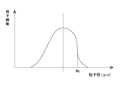
- FIG. 2A is a graph schematically showing the particle size distribution of the conductive particles supplied to the opening
- FIG. 2B is a schematic diagram showing the particle size distribution of the conductive particles held in the opening. It is a graph shown in.
- FIG. 3 is a graph schematically showing another example of the particle size distribution of the conductive particles held in the opening.
- FIG. 4 is a graph schematically showing another example of the particle size distribution of the conductive particles held in the opening.
- FIG. 5 is a graph schematically showing another example of the particle size distribution of the conductive particles held in the opening.
- FIG. 1 is a cross-sectional view schematically showing a state where conductive particles are supplied onto a member having a plurality of openings.
- FIG. 2A is a graph schematically showing the particle size distribution of the conductive particles supplied to the opening
- FIG. 2B is
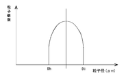
- FIG. 6A is a graph schematically showing the particle size distribution of conductive particles selected from the lower limit side of the particle size supplied to the opening, and FIG. 6B shows the conductivity held in the opening. It is a graph which shows the particle size distribution of particles typically.
- FIG. 7 is a graph schematically showing another example of the particle size distribution of the conductive particles held in the opening.
- FIG. 8 is a cross-sectional view schematically showing a state in which the adhesive film is opposed to the transfer step.
- FIG. 9 is a cross-sectional view schematically showing a method for manufacturing a connection body according to the present embodiment.
- FIG. 9A shows an arrangement step (S1)
- FIG. 9B shows a curing step ( S2).
- FIG. 1 is a cross-sectional view schematically showing a state where conductive particles are supplied onto a member having a plurality of openings.
- the member 10 is a mold having an opening having an opening size S having a predetermined opening diameter or opening width.
- the mold include metal materials such as stainless steel, transparent inorganic materials such as glass, and organic materials such as poly (meth) acrylate and crystalline resin.
- the opening forming method can be formed by various known techniques. For example, it may be provided by machining, photolithography may be used, or a printing method may be used, and there is no particular limitation.
- the mold can take various shapes such as a plate shape and a roll shape, and is not particularly limited.
- the opening accommodates conductive particles therein, and examples of the shape of the opening include a columnar shape, a polygonal column shape such as a quadrangular column, and a pyramid shape such as a conical shape and a quadrangular pyramid.
- the positions of the openings on the member that is, the positions of the conductive particles arranged in a plane view on the anisotropic conductive film preferably have a specific shape and have regularity, such as a lattice shape, a staggered shape, etc.
- the lattice shape includes an orthorhombic lattice, a hexagonal lattice, a tetragonal lattice, a rectangular lattice, and a parallel lattice. Moreover, you may have regularity with the predetermined arrangement
- the opening size S can be set based on the particle size of the conductive particles arranged on the anisotropic conductive film.
- the ratio of the opening diameter to the desired particle diameter of the conductive particles is preferably 1 from the balance of the ease of accommodating the conductive particles, the ease of pushing in the insulating resin, and the like. .1 to 2.0, more preferably 1.3 to 1.8.
- the ratio of the particle diameter of the conductive particles to the depth of the opening is preferably 0.4 to 3 in view of the balance between the improvement in transferability and the conductive particle retention. 0.0, more preferably 0.5 to 1.5.
- the diameter and depth of the opening can be measured with a laser microscope.
- the average particle diameter of the conductive particles used in the production process can be measured by an image type or laser type particle size distribution meter.
- the use of an image-type particle size distribution meter is preferable because an accurate particle size (particle diameter) can be obtained.
- An example of the image type particle size distribution measuring apparatus is FPIA-3000 (Malvern).
- the opening size S is preferably such that 60% or more of all openings have the same size, more preferably 80% or more of all openings have the same size, and all of the openings have the same size. More preferably.
- the size of the opening is different, any of the plurality of conductive particle diameters is easily held, and when the size of the opening is the same, the particle diameter of the obtained anisotropic conductive film is uniform. Prone. In any case, conductive particles that are significantly larger than the opening are not substantially held in the opening.
- the slope is substantially infinite within the range of the particle size of the maximum peak or more. A graph shape can be obtained.
- the conductive particles having a relatively small size that contributes to the connection may be insufficiently pinched, but the conduction performance is expected to be improved because the conductive particles become a conduction point, and larger conductive particles are used. Since clamping can be controlled within a certain range, it can be expected that a good connection state can be easily obtained. Since this is a metal-coated resin particle, since it is compressed, the compression state can be controlled, and more effects can be expected. It is also possible to reduce the compression hardness and set relatively small conductive particles to the target size for anisotropic connection. Thus, the choice for obtaining conduction performance increases by adjusting the compression hardness of the conductive particles.
- an opening having an opening size S having an upper limit or a lower limit of the ratio of the opening diameters described above may be adjacent, and an opening having an opening size S having an upper limit or a lower limit is anisotropic.
- You may provide periodically in the direction used as the longitudinal direction of a conductive film. This repeating unit of periodicity may be set from the width of the bump and the space between the bumps (L / S). If the arrangement of the openings is set so that the conductive particles are present in the bumps in consideration of the width of the bumps and the space between the bumps, the conductive particles can be reliably arranged at the positions sandwiched by the bumps.
- the distance between the openings can be set as appropriate, but is preferably 0.5 times or more the maximum conductive particle diameter for the purpose of arrangement, and can be set to be equal to or more than the same. In consideration of the presence of relatively small conductive particles, the distance between the openings may be 1.5 times or more, preferably 2 times or more, the maximum conductive particle diameter to be arranged. This can be set as appropriate depending on the size of the conductive particles and the size of the conductive particles to be used and the proportion of the conductive particles used.
- the minimum and maximum openings may be repeated in pairs.
- a plurality of openings having a size between the maximum and minimum may be provided simultaneously.
- any size of conductive particles may be disposed on the anisotropic conductive film, and some may not be disposed. In other words, even if one of them is missing, conduction can be satisfied if the other is present.
- each is preferably 5 or more, more preferably 10 or more, and even more preferably 12 each.
- the distance between the conductive particles is preferably 0.5 times or more, more preferably equal to or more than the maximum conductive particle diameter.
- the arrangement is generally present in a direction perpendicular to the longitudinal direction of the film. This is to satisfy the supplement to one bump. If the conductive particles are arranged in this way, practically any one is supplemented at the time of connection, so that occurrence of poor conduction can be avoided. For example, if the connection surface of the terminal (for example, the connection surface of the Au bump of the IC chip) irregularly has a non-smooth irregular shape, if there is such a pair, any conductive particles will be appropriately You can expect to be supplemented. If it is acceptable that the bumps are not smooth, it is likely to receive cost merit of obtaining a connection body, such as an improvement in yield at the time of bump manufacture and an expansion of an allowable range of design quality.
- the effect of reducing the amount of Au itself can be expected.
- the terminal connection surface has irregular irregularities that are not smooth, if the conductive particles are metal-coated resin particles, they will be compressed, so it can be handled by adjusting the compression hardness Conceivable.
- the surface area increases, so if there are those with different sizes of conductive particles, the connecting surface and the conductive particles are more than those of a single size. It is assumed that the number of contacts with will increase.
- the terminal connection surface is smooth, the effects as described above can be expected by adjusting the particle diameter and the compression hardness.
- the above effects can be avoided by adjusting the arrangement position and number density of the conductive particles in addition to the difference between the maximum and minimum conductive particle diameters and the hardness (compression hardness) of the conductive particles. It is premised on being within an allowable range.
- the method for accommodating the conductive particles in the opening is not particularly limited, and a known method can be employed. For example, by spraying or applying a dried conductive particle powder or a dispersion liquid in which the conductive particle powder is dispersed in a solvent on the opening forming surface of the member 10, the surface of the opening forming surface is squeezed using a brush, a blade, or the like.
- the conductive particles can be accommodated in the opening.
- the conductive particles 20a and 20b smaller than the opening size S are accommodated in the opening, but the conductive particles 20c larger than the opening size S are accommodated in the opening. Sorting can be performed except for conductive particles which are not accommodated and have a large particle size. Thereby, manufacturing cost can be reduced. Further, the cost can be reduced by collecting and reusing the conductive particles after the squeegee.
- the conductive particles those used in known anisotropic conductive films can be appropriately selected and used. Examples thereof include metal particles such as nickel, copper, silver, gold, and palladium, and metal-coated resin particles in which the surfaces of resin particles such as polyamide and polybenzoguanamine are coated with a metal such as nickel.
- the size of the conductive particles to be disposed is preferably 0.5 to 50 ⁇ m, and more preferably 1 to 30 ⁇ m.
- the average particle size of the conductive particles supplied in the holding step (A) is preferably such that the particle size of 0.5 to 50 ⁇ m accounts for 90% or more of the total particle amount from the viewpoint of handleability during production. In addition, it is preferable that the conductive particles less than 1 ⁇ m and larger than 30 ⁇ m are removed in the holding step. As described above, the average particle diameter can be measured by an image type particle size distribution meter, and may be measured from surface observation (surface field observation) after the holding step.
- the surface of the conductive particles is covered with an insulator. Even if the opening size S is slightly larger than the conductive particles, the conductive particles have a surface coating that is easy to peel off and does not interfere with the anisotropic connection, such as an insulating coat or an insulating particle treatment. Can be easily accommodated inside the opening. Since the thickness of such a surface coating varies depending on the connection object, there is no particular limitation as long as it does not hinder the connection.
- the protrusions are preferably within 20%, preferably within 10% of the minimum conductive particle diameter.
- the protrusions are preferably within 20%, preferably within 10% of the minimum conductive particle diameter.
- the conductive particles have relatively high compressibility. That is, it is preferable to use metal-coated resin particles.
- the hardness varies depending on the connection object, and is not particularly limited.
- the compression hardness (K value) at 20% deformation may be in the range of 1000 to 8000 N / mm 2 , and 1000 to 4000 N / mm. A range of 2 is preferred.
- the conductive particles may be intentionally mixed with those having different hardness.
- the compression hardness (K value) at the time of 20% deformation is when the conductive particles are compressed by loading in one direction and the particle size of the conductive particles becomes 20% shorter than the original particle size.
- K (3 / ⁇ 2) F ⁇ S -8/2 ⁇ R -1/2 (1) (Wherein, F: load at the time of 20% compression deformation of conductive particles S: compression displacement (mm) R: radius of conductive particles (mm))
- FIG. 2A is a graph schematically showing the particle size distribution of the conductive particles supplied to the opening
- FIG. 2B is a schematic diagram showing the particle size distribution of the conductive particles held in the opening. It is a graph shown in.
- This particle size distribution graph is a number distribution obtained by measuring the maximum length (particle size) of 1000 or more, preferably 5000 or more conductive particles by surface field observation with an optical microscope or a metal microscope.
- the present method uses a particle whose lower limit side is classified because the particle size distribution of the conductive particles supplied to the opening may be wide (or broad). The effect of facilitating the balance between performance and cost, etc. can be expected, and there is an advantage that choices of availability increase.
- conductive particles having a wide particle size distribution are supplied to the openings, but as shown in FIG. 2 (B), conductive particles held in the openings.
- the particle size distribution graph (X axis: particle size [ ⁇ m], Y axis: number of particles) has a graph shape in which the slope is substantially infinite in a range equal to or larger than the maximum peak particle size.
- the threshold Da is approximately parallel to the Y-axis where the inclination is substantially infinite.
- the fact that the inclination is substantially infinite means that the particle has a straight line parallel to the Y axis, and includes those that approximate a straight line parallel to the Y axis.
- the fact that the inclination is substantially infinite can be paraphrased as having a vertical tangent.
- the particle size distribution of the conductive particles held in the opening is not limited to the graph shape shown in FIG. 2B, and for example, as shown in FIG. 3, the inclination is substantially equal to the maximum peak particle size Db. 4 may be infinite, and as shown in FIG. 4, there may be some conductive particles having a particle diameter Dc or more in which the inclination is substantially infinite.
- there is an upper limit on the particle size of the conductive particles and since the number of particles near the upper limit is relatively small, the number of conductive particles that are insufficiently pushed in is relatively reduced, so that the occurrence of poor conduction can be suppressed. .
- the particle size distribution of the conductive particles held in the opening has a shape in which a plurality of peaks exist (the bottom exists between the peaks), and the inclination is substantially equal to the particle size Dd. It may be infinite.
- the case where there are a plurality of peaks includes, for example, a case where two types of metal-coated resin particles having different particle diameters are mixed, and the contact between the connection surface and the conductive particles is adjusted by adjusting the compression hardness of the metal-coated resin particles. It is possible to increase the conduction performance.
- the conductive particles to be supplied that are classified on the lower limit side of the particle diameter.
- Conductive particles with a small particle size do not contribute to the connection, so there is not much influence on the conductivity. This is a trade-off between costs, but a relatively large number of conductive particles are required.
- unnecessary superposition of conductive particles (overlap of conductive particles in the thickness direction) and the like can be suppressed.
- conductive particles having a relatively small size contributing to the connection are often held in the opening, and the size contributing to the connection is relatively large. It can be expected that the effect of a spacer that controls the holding of larger conductive particles than the smaller conductive particles in a certain range can be easily adjusted.
- a wet classification method in which vibration having an amplitude of 0.2 to 40 ⁇ m is applied to conductive particles in a liquid and a standard deviation of a short diameter is 10% or less can be cited (for example, JP-A-11-319626). For example).
- FIG. 6A is a graph schematically showing the particle size distribution of the conductive particles classified on the lower limit side of the particle size supplied to the opening, and FIG. 6B shows the conductivity held in the opening. It is a graph which shows the particle size distribution of particles typically.
- the particle size distribution graph (X axis: particle size [ ⁇ m], Y axis: particle amount) of the conductive particles supplied as shown in FIG. 6 (A)
- the inclination is substantially within the range of the maximum peak particle size or less.
- the particle diameter De is preferably infinite.
- the particle size distribution graph (X axis: particle size [ ⁇ m], Y axis: number of particles) of the conductive particles held in the opening is equal to or smaller than the maximum peak particle size.
- the particle diameter Df has a particle diameter Df in which the gradient is substantially infinite in the range, and has a particle diameter Dg in which the gradient is substantially infinite in a range equal to or larger than the particle diameter of the maximum peak.
- the particle size distribution graph (X axis: particle size [ ⁇ m], Y axis: number of particles) of the conductive particles held in the opening slopes within a range equal to or smaller than the maximum peak particle size.
- the conductive particles held in the openings are all within a range of ⁇ 30% of the average particle diameter. It is preferable that 90% or more of the number of particles is present, and it is more preferable that 90% or more of the total number of particles is present in the range of ⁇ 20% of the average particle diameter.
- the capture rate of the conductive particles captured by the bumps can be improved.
- the present technology is not limited to the shape of the particle size distribution graphs shown in FIGS. 2 to 7 and can take various shapes without departing from the gist of the present technology.
- the graph shape shown in FIG. 7 is a symmetric warhead type, but may not be symmetric.
- the adhesive film 30 a known anisotropic conductive film used as an insulating binder layer can be appropriately selected and used.
- the curing type of the adhesive film 30 include a thermosetting type, a photocuring type, and a photothermal combined curing type.
- a cationically polymerizable resin layer, a thermal anionic polymerizable resin layer containing an epoxy compound and a thermal anionic polymerization initiator, or a cured resin layer thereof can be used.
- the anion curable adhesive film contains a film-forming resin, an epoxy resin, and an anionic polymerization initiator.
- the film-forming resin corresponds to, for example, a high molecular weight resin having an average molecular weight of 10,000 or more, and preferably has an average molecular weight of about 10,000 to 80,000 from the viewpoint of film formation.
- the film-forming resin include various resins such as phenoxy resin, polyester resin, polyurethane resin, polyester urethane resin, acrylic resin, polyimide resin, and butyral resin. These may be used alone or in combination of two or more. May be used. Among these, it is preferable to use a phenoxy resin from the viewpoints of film formation state, connection reliability, and the like.
- the epoxy resin forms a three-dimensional network structure and imparts good heat resistance and adhesiveness, and it is preferable to use a solid epoxy resin and a liquid epoxy resin in combination.
- the solid epoxy resin means an epoxy resin that is solid at room temperature.
- the liquid epoxy resin means an epoxy resin that is liquid at room temperature.
- the normal temperature means a temperature range of 5 to 35 ° C. defined by JISZ 8703.
- the solid epoxy resin is not particularly limited as long as it is compatible with a liquid epoxy resin and is solid at room temperature.
- Bisphenol A type epoxy resin bisphenol F type epoxy resin, polyfunctional type epoxy resin, dicyclopentadiene type epoxy resin , Novolak phenol type epoxy resin, biphenyl type epoxy resin, naphthalene type epoxy resin, and the like.
- one kind can be used alone, or two or more kinds can be used in combination.
- the liquid epoxy resin is not particularly limited as long as it is liquid at normal temperature, and examples thereof include bisphenol A type epoxy resin, bisphenol F type epoxy resin, novolac phenol type epoxy resin, naphthalene type epoxy resin, and the like. Can be used alone or in combination of two or more. In particular, it is preferable to use a bisphenol A type epoxy resin from the viewpoint of film tackiness and flexibility.
- anionic polymerization initiator a commonly used known curing agent can be used.
- one kind can be used alone, or two or more kinds can be used in combination.
- it is preferable to use a microcapsule type latent curing agent having an imidazole-modified product as a core and a surface thereof coated with polyurethane.
- a stress relaxation agent examples include a hydrogenated styrene-butadiene block copolymer and a hydrogenated styrene-isoprene block copolymer.
- the silane coupling agent examples include epoxy, methacryloxy, amino, vinyl, mercapto sulfide, and ureido.
- the inorganic filler examples include silica, talc, titanium oxide, calcium carbonate, magnesium oxide and the like.
- This adhesive film 30 can be formed by forming a coating composition containing the above-described resin into a film by a coating method and drying it, or by further curing it, or by previously forming a film by a known method. .
- the thickness of the adhesive film 30 is preferably 1 to 30 ⁇ m, more preferably 2 to 15 ⁇ m. In addition, you may laminate
- the adhesive film 30 is preferably formed on a release film 40 such as a polyethylene terephthalate film subjected to a release treatment.
- Pressure may be applied to the adhesive film 30 from the release film 40 side, and the insulating binder layer may be pushed into the opening, or may be transferred so that the conductive particles 20 are embedded in the surface of the insulating binder layer.
- the particles may be pushed into the insulating binder layer.
- the adhesive film 30 may be laminated as described above before and after these steps. Thereby, a structure in which the conductive particles 20 are arranged in a single layer in the planar direction of the insulating binder layer is formed. In addition, it is preferable that the conductive particles are in a position close to the outermost surface of the adhesive film 30 in order to satisfy the supplement at the time of connection.
- the minimum melt viscosity of the entire insulating binder layer is preferably 100 to 10,000 Pa ⁇ s. Within this range, the conductive particles can be precisely arranged in the insulating binder layer, and it is possible to prevent the resin flow from hindering the trapping property of the conductive particles due to the pressing during anisotropic conductive connection.
- This minimum melt viscosity is determined by using a measuring plate having a diameter of 8 mm, using a rotary rheometer (manufactured by TA Instruments Inc.) as an example, keeping the heating rate constant at 10 ° C./min, measuring pressure at 5 g. Can do.
- the anisotropic conductive film according to the present embodiment includes an insulating binder formed in a film shape, and a plurality of conductive particles arranged in a field of view on the insulating binder, and a particle size distribution graph of the conductive particles ( In the X axis: particle diameter [ ⁇ m], Y axis: number of particles), the graph has a shape in which the slope is substantially infinite in a range equal to or larger than the maximum peak particle diameter.
- the particle size of the X axis is preferably in the range of 1 to 30 ⁇ m.
- This particle size distribution graph is a number distribution obtained by measuring the maximum length (particle size) of 1000 or more, preferably 5000 or more conductive particles by surface field observation with an optical microscope or a metal microscope.
- the shape of the particle size distribution graph of the conductive particles (X axis: particle size [ ⁇ m], Y axis: number of particles) is broad.
- the broad shape which means that the difference between the number cumulative 10% particle diameter D 10 and the number 90% cumulative particle diameter D 90 of from the particle diameter is smaller side is greater than 1 ⁇ m in cumulative distribution.
- the broad shape the difference between the number cumulative 10% particle diameter D 10 and the number 90% cumulative particle diameter D 90 from the side of its small particle size in cumulative distribution is greater than 25% of the average grain size Means.
- the cumulative number of 10% refers to the size (particle diameter) in the number of 10%, rearranged in the order of size (particle diameter) with the total number of particles measured as 100%.
- the conductive particles accommodated in the openings become conductive particles arranged in a plane view on the anisotropic conductive film. That is, as described with reference to the particle size distribution graphs shown in FIGS. 2 to 7, the anisotropic conductive film according to the present embodiment has conductive particles arranged on the upper limit side of the particle size, and the conductive film Since there is an upper limit in the particle size of the particles and the number of particles near the upper limit is large, the occurrence of poor conduction can be suppressed. Note that the conductive particles having a small particle diameter do not contribute to the connection and thus have little influence on the conductivity.
- conductive particles having a wide particle size distribution that is, non-classified or minimum classified conductive particles can be used, it is possible to contribute to reduction of material cost.
- the effect of improving the conduction characteristics can be expected by adjusting the size and hardness (compression hardness) of the conductive particles.
- the particle size distribution graph (X axis: particle diameter [ ⁇ m], Y axis: number of particles) of the conductive particles arranged on the anisotropic conductive film.
- X axis particle diameter [ ⁇ m]
- Y axis number of particles
- the conductive particles having different hardnesses when the conductive particles having different hardnesses are mixed, such a shape can be intentionally formed.
- the hardness is relatively small and the peak having a relatively small particle diameter is used, and the non-hardness is a peak having a relatively large particle diameter, an effect of increasing the supplementary efficiency can be expected.
- the indentation of the conductive particles can be adjusted, contributing to conduction stability.
- the particle diameters of the conductive particles may be measured in advance before the holding step, and simple selection may be performed for each to adjust to a generally appropriate peak. Or you may prepare what shows different particle diameter distribution in each, and may mix it so that it may become a suitable peak in general.
- the inclination is substantially within a range equal to or less than the maximum peak particle size. It is preferable to have an infinite particle size.
- the particle size distribution graph (X axis: particle size [ ⁇ m], Y axis: number of particles) of the conductive particles held in the opening is equal to or smaller than the maximum peak particle size.
- the particle diameter Df has a particle diameter Df in which the gradient is substantially infinite in the range, and has a particle diameter Dg in which the gradient is substantially infinite in a range equal to or larger than the particle diameter of the maximum peak. Further, in order to make the pressure of the conductive particles uniform at the time of pressure bonding, it is preferable that 90% or more of the total number of particles is present in the range of ⁇ 30% of the average particle diameter, and the entire range is within ⁇ 20% of the average particle diameter. It is preferable that 90% or more of the number of particles is present. As described above, by using the conductive particles obtained by classifying the lower limit side of the particle diameter in advance, the capture rate of the conductive particles captured by the bumps can be improved.
- the allowable range of the removal rate of the anisotropic conductive film varies depending on the bump layout of the connection object.
- the drop-off rate is the existence ratio of the number of conductive particles in the length in the width direction of the film and the length in the longitudinal direction. For example, if the bumps are arranged at a high density like COG, the missing rate needs to be small. For example, if the bump area is relatively large like FOG, the missing rate is large. There is no problem.
- this bias is required to be small for COG, and even if it is large to some extent for FOG, there is no problem.
- the use length and width of ACF per one time vary depending on the connection object, but generally the maximum is about 20 mm ⁇ 2 mm. Therefore, if the conductive particle diameter is 10 ⁇ m or less, the continuous area of 2 times, preferably 5 times, and more preferably 10 times of 40 mm 2 is defined as the total area of the anisotropic conductive film, and any of the areas is arbitrary. If there is no significant difference (bias) from the extracted 1 mm 2 , the connection will not be hindered.
- This 1 mm 2 is preferably extracted at 10 locations by extracting (not continuously) an area of 50 ⁇ m in the film longitudinal direction and 200 ⁇ m in the film width direction.
- the area to be evaluated is preferably a rectangular shape with a short longitudinal direction of the film.
- the conductive particle diameter is larger than 10 ⁇ m and not more than 30 ⁇ m, the entire area of the film is left as it is, the film longitudinal direction and the width direction of the area to be extracted are each doubled, and 10 areas that are not 100 ⁇ m ⁇ 400 ⁇ m in area are not continuous. A total of 4 mm 2 may be evaluated by extraction. When the film width is less than 400 ⁇ m, the rectangular shape may be changed as appropriate.
- Such a gap is preferably 50% or more, more preferably 60% or more, and more preferably 70% or more with respect to the maximum value of the number density at 10 locations of 50 ⁇ 200 ⁇ m or 100 ⁇ 400 ⁇ m. Even more preferably.
- the total of the arbitrarily extracted areas is preferably a difference of (1 mm 2 ) ⁇ 30% with respect to the conductive particle number density of the entire area, and may be a difference of ⁇ 20%. More preferable. Within this numerical range, it becomes easy to obtain both cost and performance.
- the anisotropic conductive film described above is preferably a film wound body wound around a roll in order to continuously connect electronic components.
- the length of the film wound body should just be 5 m or more, and it is preferable that it is 10 m or more. Although there is no particular upper limit, it is preferably 5000 m or less, more preferably 1000 m or less, and even more preferably 500 m or less from the viewpoint of handleability of the shipment.
- the film winding body may be one in which anisotropic conductive films shorter than the entire length are connected and connected with a tape. There may be a plurality of connected locations, may exist regularly, or may exist randomly.
- the thickness of the connecting tape is not particularly limited as long as it does not hinder the performance, but if it is too thick, it affects the protrusion and blocking of the resin, and is preferably 10 to 40 ⁇ m.
- the width of the film is not particularly limited, but is 0.5 to 5 mm as an example.
- a method for manufacturing a connection structure according to an embodiment of the present technology includes an insulating binder formed in a film shape and a plurality of conductive particles arranged in a planar view on the insulating binder, and a particle size distribution graph (X In the axis: particle diameter [ ⁇ m], Y axis: number of particles), the first electron passes through the anisotropic conductive film having a graph shape in which the inclination is substantially infinite in the range equal to or larger than the maximum peak particle diameter.
- Arrangement step (S1) for placing the component and the second electronic component, and a curing step (S2) for crimping the second electronic component to the first electronic component by the crimping tool and curing the anisotropic conductive film And have.
- FIG. 9 is a cross-sectional view schematically showing a method for manufacturing a connection body according to the present embodiment.
- FIG. 9A shows an arrangement step (S1)
- FIG. 9B shows a curing step ( S2).
- an anisotropic conductive adhesive film is the same as that of the above-mentioned, description is abbreviate
- the first electronic component 50 includes a first terminal row 51.
- the first electronic component 50 includes LCD (Liquid Crystal Display) panels, flat panel display (FPD) applications such as organic EL (OLED), transparent substrates for touch panel applications, printed wiring boards (PWB), and the like. It is done.
- the material of the printed wiring board is not particularly limited. For example, glass epoxy such as FR-4 base material, plastic such as thermoplastic resin, ceramic, or the like can be used.
- the transparent substrate is not particularly limited as long as it has high transparency, and examples thereof include a glass substrate and a plastic substrate.
- the second electronic component 70 includes a second terminal row 71 that faces the first terminal row 51.
- the 2nd electronic component 70 does not have a restriction
- the second electronic component 70 include an IC (IntegratedIntegrCircuit), a flexible substrate (FPC: Flexible Printed Circuits), a tape carrier package (TCP) substrate, and a COF (Chip On Film) having an IC mounted on the FPC. It is done.
- connection structure manufacturing method excellent conductivity can be obtained as in the case of using an anisotropic conductive film containing conductive particles classified in advance.
- connection structure includes a first electronic component, a second electronic component, and an adhesive film in which the first electronic component and the second electronic component are bonded.
- an insulating binder formed in a film shape, and a plurality of conductive particles arranged in a field of view on the insulating binder, and a particle size distribution graph of the conductive particles (X axis: particle diameter [ ⁇ m], Y axis) : Number of particles), the anisotropic conductive film having a graph shape in which the inclination is substantially infinite in a range equal to or larger than the maximum peak particle diameter is cured.
- connection structure excellent conductivity can be obtained as in the case of bonding using an anisotropic conductive film containing conductive particles classified in advance.
- this technique is applicable not only to the application to the manufacturing method of the connection structure mentioned above but also when stacking IC chips and wafers to make a multilayer.
- Manufacturing method of filler-arranged film and filler-arranged film> The manufacturing method of the anisotropic conductive film mentioned above can manufacture the filler arrangement
- the method for producing a filler-arranged film supplies a filler having a plurality of particle diameters on a member having a plurality of openings, and holds the filler in the openings, and the openings.
- the graph has a gradient that is substantially infinite in a range equal to or larger than the particle diameter.
- this method balances performance and cost, such as using a particle whose lower limit is classified. There is an advantage that the effect of facilitating the expectation can be expected, and the options of availability increase.
- an inorganic filler or an organic filler can be used depending on the use of the filler-arranged film.
- the inorganic filler include silica, calcium carbonate, talc, barium sulfate, aluminum hydroxide, aluminum oxide, magnesium hydroxide, magnesium oxide, titanium oxide, zinc oxide, iron oxide, mica and the like.
- organic filler well-known resin fillers, such as a silicone resin, a fluororesin, and a polybutadiene resin, rubber particles, etc. are mentioned, for example.
- examples of the filler include silica, calcium carbonate, known resin fillers, rubber particles, and the like, and the filler-arranged film is excellent because the particle diameter of the filler is uniform. Functions as a gap spacer.
- examples of the filler include titanium oxide, zinc oxide, iron oxide, or a known resin filler. Is arranged at a predetermined position in the surface field of view, so that excellent optical performance can be obtained.
- examples of the filler include colored fillers (regardless of inorganic and organic substances), and the filler-arranged film is arranged at a predetermined position in a plane view, Excellent design properties can be obtained.
- the member having a plurality of openings and the adhesive film are the same as those described in the method for manufacturing the anisotropic conductive film described above, description thereof is omitted here.
- the filler-arranged film according to the present embodiment includes an insulating binder formed in a film shape and a plurality of fillers arranged in a plane field of view on the insulating binder, and a particle size distribution graph of the filler (X axis: particles) In the diameter [ ⁇ m], the Y axis: the number of particles), the graph has a shape in which the slope is substantially infinite in a range equal to or larger than the maximum peak particle size.
- the filler particle size distribution is cut with a large particle size and arranged in a plane view.
- a conductive member other than the method of using an anisotropic conductive film known as a conductive particle It can be set as the use to be used, a gap spacer, an optical member, a design member, or the like.
- the conductive particles mixed at a predetermined ratio (number conversion) are supplied to the resin mold on which the opening array pattern is formed, the conductive particles are held in the openings, and the conductive particles held in the openings are bonded.
- An anisotropic conductive film was produced by transferring to a film. And classification evaluation of the anisotropic conductive film was performed.
- the connection structure was produced using the anisotropic conductive film, and the continuity evaluation, the supplementary evaluation, and the short evaluation of the connection structure were performed. Note that the present technology is not limited to these examples. For example, the effect similar to the result of the classification evaluation of an anisotropic conductive film is obtained also about the manufacturing method of the filler arrangement
- the height of the convex portion (that is, the depth of the opening) was 3.5 ⁇ m.
- a known transparent resin pellet was poured into this mold in a molten state, and cooled and hardened to form a resin mold having an opening array pattern.
- the opening depth of the obtained resin mold was almost the same as the height of the convex portion.
- a resin composition A having the following composition was coated on a PET film having a film thickness of 50 ⁇ m with a bar coater and dried in an oven at 80 ° C. for 5 minutes to form an insulating resin layer A having a thickness of 4 ⁇ m on the PET film. .
- Resin composition A (insulating resin layer A) Phenoxy resin (YP-50, Nippon Steel & Sumikin Chemical Co., Ltd.): 30 parts by mass, epoxy resin (jER828, Mitsubishi Chemical Co., Ltd.): 40 parts by mass, cationic curing agent (SI-60L, Sanshin Chemical Industry Co., Ltd.) ): 2 parts by mass, filler (Aerosil RX300, Nippon Aerosil Co., Ltd.): 30 parts by mass
- a resin composition B having the following composition was coated on a PET film having a film thickness of 50 ⁇ m with a bar coater and dried in an oven at 80 ° C. for 5 minutes to form an insulating resin layer B having a thickness of 14 ⁇ m on the PET film. .
- Resin composition B (insulating resin layer B) Phenoxy resin (YP-50, Nippon Steel & Sumikin Chemical Co., Ltd.): 30 parts by mass, Phenoxy resin (FX-316ATM55, Nippon Steel & Sumikin Chemical Co., Ltd.): 30 parts by mass, epoxy resin (jER828, Mitsubishi Chemical Co., Ltd.): 40 parts by mass, cationic curing agent (SI-60L, Sanshin Chemical Industry Co., Ltd.): 2 parts by mass
- 3 ⁇ m metal-coated resin particles (Sekisui Chemical Co., Ltd., AUL703, average particle diameter of 3 ⁇ m, hereinafter referred to as “3 ⁇ m diameter particles”), and 5 ⁇ m metal-coated resin particles (Sekisui Chemical Co., Ltd.) AUL705, an average particle diameter of 5 ⁇ m, and hereinafter referred to as “5 ⁇ m diameter particles”) were prepared.
- Conductive particles A were obtained by weighing into a container such that 3 ⁇ m diameter particles were 80% in terms of number and 5 ⁇ m diameter particles were 20% and mixed well. To confirm the mixing, a small amount of the mixture was taken out, spread on an adhesive film, and observed with a metal microscope. This was repeated 3 to 10 times to confirm that the mixed state was uniform.
- the conductive particles A are filled in the resin-type depressions in which the opening array pattern is formed, and the insulating resin layer A is covered thereon and pressed at 60 ° C. and 0.5 MPa, so that the conductive particles A are insulated from the resin. The layers were stuck. Then, the insulating resin layer A is peeled off from the resin mold, and the conductive particles on the insulating resin layer A are pressurized (pressing conditions: 60 to 70 ° C., 0.5 Mpa) to thereby remove the conductive particles A from the insulating resin. It pressed into the layer A and produced the conductive particle content layer.
- Conductive particles B mixed such that 3 ⁇ m diameter particles are 75% in terms of number and 5 ⁇ m diameter particles are 25%, and mixed so that 3 ⁇ m diameter particles are 50% in terms of number and 5 ⁇ m diameter particles are 50%.
- Conductive particles C, conductive particles D mixed such that 3 ⁇ m diameter particles are 40% in terms of number and 5 ⁇ m diameter particles are 60%, and conductive particles E in which 3 ⁇ m diameter particles are 100% in terms of number are also described above.
- anisotropic conductive films B to E were produced.
- the anisotropic conductive films A to D had a particle omission in the arrangement as the number ratio of 3 ⁇ m diameter particles of the used conductive particles was lower, but anisotropic using only 3 ⁇ m diameter particles as described later.
- the same performance as that of the conductive conductive film E was exhibited, and there was no practical problem.
- the particle size distribution of the conductive particles in the conductive particle-containing layers in the anisotropic conductive films A to E was measured using a particle size distribution measuring apparatus (FPIA-3000 (Malvern)).
- connection structure [Evaluation of continuity of connection structure]
- the anisotropic conductive films A to E were sandwiched between the conductivity evaluation IC and the glass substrate, and heated and pressurized (180 ° C., 60 MPa, 5 seconds) to produce a connection structure for conductivity evaluation. And the conduction resistance of each connection structure was measured after the reliability test which left still for 500 hours at the initial stage after connection, and the temperature 85 degreeC and the humidity 85% RH.
- the initial conduction resistance was less than 0.5 ⁇ , and the conduction resistance after the reliability test was less than 5 ⁇ . That is, the anisotropic conductive films A to D showed the same performance as the anisotropic conductive film E using only 3 ⁇ m diameter particles, and it was found that there is no practical problem.
- Conductivity evaluation IC Outline 1.8 ⁇ 20.0mm Thickness 0.5mm Bump specifications Size 30 ⁇ 85 ⁇ m, distance between bumps 50 ⁇ m, bump height 15 ⁇ m
- connection structure for conductivity evaluation, an indentation inspection was performed on the captured state of the conductive particles. As a result, in all of the anisotropic conductive films A to E, it was confirmed that at least three or more conductive particles per bump were independent indentations. As for the number of traps, the higher the mixing ratio of 3 ⁇ m diameter particles, the greater the number of captures, and the anisotropic conductive film E using only the 3 ⁇ m diameter had the largest number of traps.
- connection structure For each connection structure for continuity evaluation, the number of shorted channels in 100 bumps was measured and taken as the number of shorts. As a result, none of the connection structures using the anisotropic conductive films A to E were short-circuited.
- anisotropic conductive films A to E are sandwiched between a short-circuit occurrence rate evaluation IC and a glass substrate having a pattern corresponding to the evaluation IC, and are heated and pressurized (180 ° C., 60 MPa, 5 seconds) to conduct.
- a connection structure for property evaluation was prepared.
- the number of channels shorted between the bumps was defined as the number of shorts, and the short-circuit occurrence rate calculated by “number of shorts / total number of 7.5 ⁇ m spaces” was obtained.
- the occurrence rate of short circuit was less than 50 ppm. Note that there is no practical problem if the short-circuit occurrence rate is less than 50 ppm.
- IC for short-circuit incidence evaluation (comb tooth TEG (Test Element Group)) External dimensions 1.5 x 13 mm Thickness 0.5mm Bump specifications Gold plating, height 15 ⁇ m, size 25 ⁇ 140 ⁇ m, distance between bumps 7.5 ⁇ m
- the anisotropic conductive films A to D to which the present technology is applied are classified into particles having a diameter of 3 ⁇ m in any of the classification evaluation of the anisotropic conductive film, the continuity evaluation of the connection structure, the supplementary evaluation, and the short evaluation. It was equivalent to the anisotropic conductive film E used, and it was found that there was no practical problem. That is, by applying the present technology, conductive particles having a broad particle size distribution can be used, and the manufacturing cost can be reduced. Moreover, it turns out that the same effect is acquired also from a filler arrangement
- the conductive particles having a large particle diameter are removed, but the conductive particles having a small particle diameter may be removed in advance by a known method.
- a method for removing conductive particles having a small particle diameter for example, a wet classification method in which vibration having an amplitude of 0.2 to 40 ⁇ m is applied to conductive particles in a liquid and a standard deviation of a short diameter is 10% or less. Etc.
Abstract
製造コストを削減することができる異方性導電フィルムの製造方法を提供する。また、導通不良の発生を抑制することができる異方性導電フィルムを提供する。異方性導電フィルムの製造方法は、複数の開口部を有する部材(10)上に、複数の粒子径の導電粒子(20a~20c)を供給し、開口部に導電粒子を保持させる保持工程と、開口部に保持された導電粒子を接着フィルムに転写する転写工程とを有し、開口部に保持された導電粒子の粒子径分布グラフ(X軸:粒子径[μm]、Y軸:粒子個数)において、最大ピークの粒子径以上の範囲で傾きが実質的に無限大となるグラフ形状となる。
Description
本技術は、導電粒子を含有する異方性導電フィルムの製造方法、及び異方性導電フィルムに関する。本出願は、日本国において2016年5月2日に出願された日本特許出願番号特願2016-092832、及び2017年4月24日に出願された日本特許出願番号特願2017-085492を基礎として優先権を主張するものであり、この出願は参照されることにより、本出願に援用される。
従来、ICチップなどの電子部品を実装する異方性導電フィルム(ACF:Anisotropic Conductive Film)が知られている。また、近年、複数の開口部を有する型を用いて、異方性導電フィルム内の導電粒子を隣接する導電粒子と個々に独立させるように離間させる、もしくは配列させることが検討されている(例えば、特許文献1参照。)。
しかしながら、複数の開口部を有する型に用いられる導電粒子は、異方性接続に支障を来たさないよう粒子径分布がシャープになるよう、分級がなされており、製造コストが高い。
また、粒子径が大きく異なる導電粒子が面視野で配置された異方性導電フィルムは、押圧時に導電粒子の押し込み不足が発生し、導通不良の原因となる。
本技術は、前述した課題を解決するものであり、製造コストを削減することができる異方性導電フィルムの製造方法を提供する。また、導通不良の発生を抑制することができる異方性導電フィルムを提供する。また、製造コストを削減することができるフィラー配置フィルムの製造方法、及びフィラー配置フィルムを提供する。
本技術者は、鋭意検討した結果、複数の開口部を有する部材を用いて導電粒子又はフィラーの選別を行うことにより、製造コストを削減することができることを見出した。また、異方性導電フィルムに面視野で配置される導電粒子の粒子径分布グラフにおいて、所定のグラフ形状となることにより、導通不良の発生を抑制することができることを見出した。
すなわち、本技術に係る異方性導電フィルムの製造方法は、複数の開口部を有する部材上に、複数の粒子径の導電粒子を供給し、前記開口部に導電粒子を保持させる保持工程と、前記開口部に保持された導電粒子を接着フィルムに転写する転写工程とを有し、前記開口部に保持された導電粒子の粒子径分布グラフ(X軸:粒子径[μm]、Y軸:粒子個数)において、最大ピークの粒子径以上の範囲で傾きが実質的に無限大となるグラフ形状となる。
また、本技術に係る異方性導電フィルムは、フィルム状に形成された絶縁性バインダーと、前記絶縁性バインダーに面視野で配置される複数の導電粒子とを備え、前記導電粒子の粒子径分布グラフ(X軸:粒子径[μm]、Y軸:粒子個数)において、最大ピークの粒子径以上の範囲で傾きが実質的に無限大となるグラフ形状となる。
また、本技術に係るフィルム巻装体は、前記異方性導電フィルムが巻き芯に巻かれている。
すなわち、本技術に係るフィラー配置フィルムの製造方法は、複数の開口部を有する部材上に、複数の粒子径のフィラーを供給し、前記開口部にフィラーを保持させる保持工程と、前記開口部に保持されたフィラーを接着フィルムに転写する転写工程とを有し、前記開口部に保持されたフィラーの粒子径分布グラフ(X軸:粒子径[μm]、Y軸:粒子個数)において、最大ピークの粒子径以上の範囲で傾きが実質的に無限大となるグラフ形状となる。
また、本技術に係るフィラー配置フィルムは、フィルム状に形成された絶縁性バインダーと、前記絶縁性バインダーに面視野で配置される複数のフィラーとを備え、前記フィラーの粒子径分布グラフ(X軸:粒子径[μm]、Y軸:粒子個数)において、最大ピークの粒子径以上の範囲で傾きが実質的に無限大となるグラフ形状となる。
本技術によれば、複数の開口部を有する部材を用いて導電粒子又はフィラーの選別を行うことにより、製造コストを削減することができる。また、異方性導電フィルムに面視野で配置される導電粒子の粒子径分布グラフにおいて、所定のグラフ形状となることにより、導通不良の発生を抑制することができる。
以下、本技術の実施の形態について、下記順序にて詳細に説明する。
1.異方性導電フィルムの製造方法
2.異方性導電フィルム
3.接続構造体の製造方法、及び接続構造体
4.フィラー配置フィルムの製造方法、及びフィラー配置フィルム
5.実施例
1.異方性導電フィルムの製造方法
2.異方性導電フィルム
3.接続構造体の製造方法、及び接続構造体
4.フィラー配置フィルムの製造方法、及びフィラー配置フィルム
5.実施例
<1.異方性導電フィルムの製造方法>
本実施の形態に係る異方性導電フィルムの製造方法は、複数の開口部を有する部材上に、複数の粒子径の導電粒子を供給し、開口部に導電粒子を保持させる保持工程(A)と、開口部に保持された導電粒子を接着フィルムに転写する転写工程(B)とを有する。以下、保持工程(A)、及び転写工程(B)について説明する。
[保持工程(A)]
本実施の形態に係る異方性導電フィルムの製造方法は、複数の開口部を有する部材上に、複数の粒子径の導電粒子を供給し、開口部に導電粒子を保持させる保持工程(A)と、開口部に保持された導電粒子を接着フィルムに転写する転写工程(B)とを有する。以下、保持工程(A)、及び転写工程(B)について説明する。
[保持工程(A)]
(開口部材)
図1は、複数の開口部を有する部材上に導電粒子が供給された状態を模式的に示す断面図である。図1に示すように、部材10は、所定の開口径又は開口幅の開口サイズSを有する開口部を有する型である。型としては、例えば、ステンレスなどの金属材料、ガラスなどの透明無機材料、ポリ(メタ)アクリレートや結晶性樹脂等の有機材料が挙げられる。開口形成方法は種々公知の技術によって形成させることができる。例えば機械加工によって設けてもよく、フォトリソグラフィを利用してもよく、印刷法を利用してもよく、特に限定はない。また、型は、板状、ロール状等種々の形状をとることができ、特に制限はされない。
図1は、複数の開口部を有する部材上に導電粒子が供給された状態を模式的に示す断面図である。図1に示すように、部材10は、所定の開口径又は開口幅の開口サイズSを有する開口部を有する型である。型としては、例えば、ステンレスなどの金属材料、ガラスなどの透明無機材料、ポリ(メタ)アクリレートや結晶性樹脂等の有機材料が挙げられる。開口形成方法は種々公知の技術によって形成させることができる。例えば機械加工によって設けてもよく、フォトリソグラフィを利用してもよく、印刷法を利用してもよく、特に限定はない。また、型は、板状、ロール状等種々の形状をとることができ、特に制限はされない。
開口部は、その内部に導電粒子を収容するものであり、開口の形状としては、円柱状、四角柱等の多角柱状、円錐状や四角錐等の角錐状等を例示することができる。開口部の部材上の位置、即ち異方性導電フィルムに平面視で配置される導電粒子の位置は、特定の形状を有して規則性を持っていることが好ましく、格子状、千鳥状等の規則的な配列とすることが好ましい。格子状としては、斜方格子、六方格子、正方格子、矩形格子、平行体格子等が挙げられる。また、フィルムの長手方向に対して所定の配列形状で規則性を持っていてもよい。
開口サイズSは、異方性導電フィルムに配置する導電粒子の粒径に基づいて設定することができる。例えば求める導電粒子の粒径に対する開口径の比(=開口の径/導電粒子の粒径)は、導電粒子の収容のしやすさ、絶縁性樹脂の押し込みやすさ等のバランスから、好ましくは1.1~2.0、より好ましくは1.3~1.8である。また、例えば開口の深さに対する導電粒子の粒径の比(=導電粒子の粒径/開口の深さ)は、転写性向上と導電粒子保持性とのバランスから、好ましくは0.4~3.0、より好ましくは0.5~1.5である。なお、開口の径と深さは、レーザー顕微鏡で測定することができる。製造工程に用いる導電粒子の平均粒子径は、画像型ないしはレーザー式の粒度分布計により測定することができる。尚、画像型の粒度分布計を用いる方が、正確な粒子の大きさ(粒子径)が得られるため好ましい。画像型の粒度分布測定装置としては、例えばFPIA-3000(マルバーン社)が挙げられる。
また、開口サイズSは、全開口部の60%以上が同じ大きさであることが好ましく、全開口部の80%以上が同じ大きさであることがより好ましく、開口部の全てが同じ大きさであることがさらに好ましい。開口部の大きさが異なることで、複数の導電粒子径のいずれかが保持されやすくなり、また開口部の大きさが同じになることで、得られる異方性導電フィルムの粒子径が均一になりやすい。また、何れにせよ開口部より著しく大きい導電粒子は、実質的には開口部に保持されないことになる。これにより、開口部に保持される導電粒子の粒子径分布グラフ(X軸:粒子径[μm]、Y軸:粒子個数)において、最大ピークの粒子径以上の範囲で傾きが実質的に無限大となるグラフ形状を得ることができる。
開口部に対して著しく小さい導電粒子がある場合、複数が開口部に保持されることが懸念されるが、下記に記載の導電粒子の収容手法によって不要な導電粒子はかき出されることになる。かき出されない場合、微小な導電粒子が一つの開口部、もしくはその近傍に連結もしくは近接して存在することになるが、接続には寄与しないか影響が小さいことがわかるため無視してもよい。これは、接続時の樹脂流動によりバンプの接続方向に重畳することはほぼなくなるためである。また、接続に寄与する大きさの比較的小さい導電粒子が存在している場合、導通性能の向上が見込まれる。これは導電粒子でありながら、端子に挟持される場合において、これよりも大きい導電粒子のスペーサーとしても働く効果が期待できる。即ち、接続に寄与する大きさの比較的小さい導電粒子は、挟持の状態は不十分であるかもしれないが、導通点となるため導通性能の向上が見込まれ、且つこれよりも大きい導電粒子の挟持を一定の範囲で制御できることから、良好な接続状態を得易くなることが期待できる。これは金属被覆樹脂粒子であれば、圧縮されることから、圧縮状態を制御できることになり、より効果が期待できるため好ましい。また、圧縮硬さを低くして、比較的小さい導電粒子を異方性接続の目的とする大きさに設定することも可能になる。このように、導電粒子の圧縮硬さの調整で、導通性能を得るための選択肢が増えることになる。
また、全開口部の一部において開口サイズSが異なる場合、規則性を持たせてもよい。例えば、前述した開口径の比の上限ないし下限の大きさの開口サイズSを有する開口部が隣接するようにしてもよく、上限もしくは下限の大きさの開口サイズSを有する開口部が異方性導電フィルムの長手方向となる方向に周期的に設けられてもよい。この周期性の繰り返し単位は、バンプの幅とバンプ間スペース(L/S)から設定してもよい。バンプの幅とバンプ間スペースを加味してバンプに導電粒子が存在するように開口部の配置を設定すれば、バンプに挟持される位置に導電粒子を確実に配置させることができる。開口部間の距離は適宜設定できるが、配置させる目的の最大の導電粒子径の0.5倍以上が好ましく、等倍以上となるように設定することができる。尚、比較的小さい導電粒子が存在することを加味すれば、開口部間の距離は配置させる目的の最大の導電粒子径の1.5倍以上、好ましくは2倍以上としてもよい。これは導電粒子の大きさと用いられる導電粒子に小さい粒子径のものがどの程度の大きさで、どの程度の割合で存在するかで、適宜設定できる。
また、接続構造体の生産不良を生じ難くし、且つ導通を確実にするためには、最小と最大の開口部がペアになって繰り返されるようになればよい。もしくは最大と最小の間の大きさの開口部を同時に複数設けてもよい。この場合、いずれかの大きさの導電粒子が異方性導電フィルムに配置されればよく、いくつかは配置されなくてもよい。即ち、何れかが抜けたとしても、もう一方が存在すれば導通を満足することができる。一例として、それぞれ5個以上ずつが好ましく、10個以上ずつがより好ましく、12個ずつが更により好ましい。導電粒子間の距離は、最大の導電粒子径の0.5倍以上が好ましく、より好ましくは等倍以上である。配置は、フィルムの長手方向と直行する方向に概ね存在するになることが好ましい。一つのバンプへの補足を満足させるためである。このように導電粒子が配置されれば、実用上いずれかが接続時に補足されるため、導通不良の発生が回避できる。例えば、端子の接続面(例えば、ICチップのAuバンプの接続面)が平滑ではない凹凸形状を不定期に有している場合において、このようなペアがあれば何れかの導電粒子が適切に補足されることが期待できる。バンプが平滑ではないことが許容できれば、バンプ製造時における歩留まりの向上や設計品質の許容範囲の拡大など、接続体を得ることのコストメリットを受け易くなる。またAuバンプの場合、Auの使用量そのものを削減できる効果も期待できる。また、端子の接続面が平滑ではない凹凸形状を不定期に有している場合も、導電粒子が金属被覆樹脂粒子であれば、圧縮されるので、圧縮硬さの調整で対応が可能だと考えられる。尚、このような凹凸形状を不定期に有している場合、表面積が増えることから、導電粒子の大きさが異なるものが存在すれば単一の大きさのものよりも、接続面と導電粒子との接点が増えると推察される。端子の接続面が平滑である場合は、粒子径と圧縮硬さの調整によって、上述したような効果が期待できる。以上のような効果は、最大と最小の導電粒子径の差分や、導電粒子の硬さ(圧縮硬さ)の他に、導電粒子の配置位置や個数密度などを調整することで不具合は回避もしくは許容範囲内にすることを前提としたものである。
開口部に導電粒子を収容する手法としては、特に限定されるものではなく、公知の手法を採用することができる。例えば、乾燥した導電粒子粉末またはこれを溶媒中に分散させた分散液を部材10の開口形成面上に散布または塗布した後、ブラシ、ブレードなどを用いて開口形成面の表面をスキージすることにより、開口部に導電粒子を収容することができる。
開口部に導電粒子を収容する際、図1に示すように、開口サイズSより小さい導電粒子20a、20bは、開口部に収容されるが、開口サイズSより大きい導電粒子20cは、開口部に収容されず、粒子径の大きい導電粒子を除く、選別を行うことができる。これにより、製造コストを削減することができる。また、スキージ後の導電粒子を回収して再利用することにより、コスト削減を図ることができる。
(導電粒子)
導電粒子としては、公知の異方性導電フィルムにおいて使用されているものを適宜選択して使用することができる。例えば、ニッケル、銅、銀、金、パラジウムなどの金属粒子、ポリアミド、ポリベンゾグアナミン等の樹脂粒子の表面をニッケルなどの金属で被覆した金属被覆樹脂粒子等を挙げることができる。配置される導電粒子の大きさは、一例として0.5~50μmであることが好ましく、1~30μmがより好ましい。
導電粒子としては、公知の異方性導電フィルムにおいて使用されているものを適宜選択して使用することができる。例えば、ニッケル、銅、銀、金、パラジウムなどの金属粒子、ポリアミド、ポリベンゾグアナミン等の樹脂粒子の表面をニッケルなどの金属で被覆した金属被覆樹脂粒子等を挙げることができる。配置される導電粒子の大きさは、一例として0.5~50μmであることが好ましく、1~30μmがより好ましい。
保持工程(A)において供給される導電粒子の平均粒子径は、製造時の取り扱い性の観点から、0.5~50μmの粒子径が全粒子量の90%以上を占めることが好ましい。尚、1μm未満、30μmより大きい導電粒子は保持工程で除かれることが好ましい。平均粒子径は、前述したように、画像型粒度分布計により測定することができ、保持工程後に面観察(面視野観察)から計測してもよい。
また、導電粒子の表面は、絶縁体によって被覆されていることが好ましい。導電粒子の表面に絶縁コートや絶縁粒子処理など、表面にはがれ易く且つ異方性接続に支障をきたさない表面被覆が存在することにより、開口サイズSが導電粒子よりも若干大きくても、導電粒子を開口部の内部に収容し易くなる。このような表面被覆の厚みは、接続対象物によって異なるため、接続に支障を来たさない限り特に制限はない。
また、導電粒子の突起が表面に設けられている場合、その突起は最小の導電粒子径の20%以内、好ましくは10%以内の大きさであることが好ましい。個数については特に制限はなく、全面に均一に設けられていてもよく、まばらに設けられていてもよい。
また、導電粒子は、粒子径の異なるものが混在しているため、比較的圧縮性の高いものであることが好ましい。即ち、金属被覆樹脂粒子を用いることが好ましい。硬さは接続対象によって変更されるため、特に制限はないが、一例として20%変形時の圧縮硬さ(K値)が1000~8000N/mm2の範囲であればよく、1000~4000N/mm2の範囲が好ましい。また、導電粒子は、硬さが異なるものが意図的に混在するようにしてもよい。
ここで、20%変形時の圧縮硬さ(K値)とは、導電粒子を一方向に荷重して圧縮することにより、導電粒子の粒子径が元の粒子径に比べて20%短くなるときの荷重から次式(1)により算出される数値であり、K値が小さいほど柔らかい粒子となる。
K=(3/√2)F・S-8/2・R-1/2 (1)
(式中、F:導電粒子の20%圧縮変形時における荷重
S:圧縮変位(mm)
R:導電粒子の半径(mm) )
K=(3/√2)F・S-8/2・R-1/2 (1)
(式中、F:導電粒子の20%圧縮変形時における荷重
S:圧縮変位(mm)
R:導電粒子の半径(mm) )
(粒子径分布)
図2(A)は、開口部に供給される導電粒子の粒子径分布を模式的に示すグラフであり、図2(B)は、開口部に保持される導電粒子の粒子径分布を模式的に示すグラフである。この粒子径分布グラフは、光学顕微鏡や金属顕微鏡の面視野観察で1000個以上、好ましくは5000個以上の導電粒子の最大長(粒子径)を測定した個数分布である。図2(A)に示すように、本法は、開口部に供給される導電粒子の粒子径分布が広くても(ブロードでも)よいことから、粒子径の下限側を分級したものを使用するなど、性能とコストのバランスを取り易くなる効果が期待でき、利用可能性の選択肢が増えるという利点がある。
図2(A)は、開口部に供給される導電粒子の粒子径分布を模式的に示すグラフであり、図2(B)は、開口部に保持される導電粒子の粒子径分布を模式的に示すグラフである。この粒子径分布グラフは、光学顕微鏡や金属顕微鏡の面視野観察で1000個以上、好ましくは5000個以上の導電粒子の最大長(粒子径)を測定した個数分布である。図2(A)に示すように、本法は、開口部に供給される導電粒子の粒子径分布が広くても(ブロードでも)よいことから、粒子径の下限側を分級したものを使用するなど、性能とコストのバランスを取り易くなる効果が期待でき、利用可能性の選択肢が増えるという利点がある。
図2(A)に示すように、本実施の形態では、粒子径分布が広い導電粒子が開口部に供給されるものの、図2(B)に示すように、開口部に保持される導電粒子の粒子径分布グラフ(X軸:粒子径[μm]、Y軸:粒子個数)は、最大ピークの粒子径以上の範囲で傾きが実質的に無限大となるグラフ形状となる。特に、同じ大きさの開口部の割合が高いほど、傾きが実質的に無限大となるY軸に略平行な閾値Daを持つこととなる。粒子径分布において、傾きが実質的に無限大とは、Y軸と並行な直線を有する、という意味であり、Y軸と平行な直線に近似しているものも含む。また、粒子径分布において、傾きが実質的に無限大とは、垂直接線(vertical tangent)を有する、と言い換えることもできる。
また、開口部に保持される導電粒子の粒子径分布は、図2(B)に示すグラフ形状に限られるものではなく、例えば図3に示すように最大ピークの粒子径Dbで傾きが実質的に無限大となってもよく、図4に示すように傾きが実質的に無限大となる粒子径Dc以上の導電粒子が若干存在してもよい。これらのグラフ形状のように導電粒子の粒径に上限があり、上限付近の粒子数が多いことにより、押し込みが不足する導電粒子が相対的に減少するため導通不良の発生を抑制することができる。
また、図5に示すように、開口部に保持される導電粒子の粒子径分布は、ピークが複数存在する(ボトムがピーク間に存在する)形状になり、粒子径Ddで傾きが実質的に無限大となってもよい。ピークが複数存在する場合とは、例えば粒子径の異なる2種の金属被覆樹脂粒子を混合した場合などが挙げられ、金属被覆樹脂粒子の圧縮硬さの調整で接続面と導電粒子との接点を増加させ、導通性能を向上させることができる。
また、供給される導電粒子は、粒子径の下限側を分級したものを使用することが好ましい。微小な粒子径の導電粒子は、接続に寄与しないため導通性への影響はあまりないため、コストとの兼ね合いになるが、導電粒子が比較的多く必要になる、COG接続などでは粒子径の下限側を分級したものを使用することにより、導電粒子の不要な重畳(厚み方向に導電粒子が重なること)などを抑制することができる。また、粒子径の下限側を分級したものを使用することにより、接続に寄与する大きさの比較的小さい導電粒子が開口部に保持されることが多くなり、接続に寄与する大きさの比較的小さい導電粒子よりも大きい導電粒子の挟持を一定の範囲で制御するスペーサーの効果などを調整し易くなることが期待できる。
粒子径の下限側の分級方法としては、種々公知の技術を用いることができる。例えば、液体中の導電粒子に0.2~40μmの振幅を有する振動を与え、短径の標準偏差が10%以下の篩により行う湿式分級方法を挙げることができる(例えば、特開平11-319626が挙げられる)。
図6(A)は、開口部に供給される粒子径の下限側を分級した導電粒子の粒子径分布を模式的に示すグラフであり、図6(B)は、開口部に保持される導電粒子の粒子径分布を模式的に示すグラフである。図6(A)に示すように供給される導電粒子の粒子径分布グラフ(X軸:粒子径[μm]、Y軸:粒子量)において、最大ピークの粒子径以下の範囲で傾きが実質的に無限大となる粒子径Deを有することが好ましい。これにより、図6(B)に示すように開口部に保持される導電粒子の粒子径分布グラフ(X軸:粒子径[μm]、Y軸:粒子個数)は、最大ピークの粒子径以下の範囲で傾きが実質的に無限大となる粒子径Dfを有するとともに、最大ピークの粒子径以上の範囲で傾きが実質的に無限大となる粒子径Dgを有することとなる。
また、図7に示すように、開口部に保持される導電粒子の粒子径分布グラフ(X軸:粒子径[μm]、Y軸:粒子個数)は、最大ピークの粒子径以下の範囲で傾きが実質的に無限大となるY軸に略平行な閾値Dhを有するとともに、最大ピークの粒子径以上の範囲で傾きが実質的に無限大となるY軸に略平行な閾値Diを有してもよい。
また、粒子径の下限側を分級したものを使用した場合、圧着時の導電粒子の圧力を均一にするため、開口部に保持される導電粒子は、平均粒子径の±30%の範囲に全粒子数の90%以上が存在することが好ましく、平均粒子径の±20%の範囲に全粒子数の90%以上が存在することがさらに好ましい。このように予め粒子径の下限側を分級した導電粒子を使用することにより、バンプに捕捉される導電粒子の捕捉率を向上させることができる。
なお、本技術は、図2~7に示す粒子径分布のグラフの形状に限られるものではなく、本技術の要旨を逸脱しない範囲内において種々の形状をとることができる。例えば、図7に示すグラフ形状は左右対称の弾頭型であるが、左右対称でなくともよい。
[転写工程(B)]
次の転写工程(B)では、先ず、図8に示すように、開口が形成された部材10表面に接着フィルム30を対向させる。
次の転写工程(B)では、先ず、図8に示すように、開口が形成された部材10表面に接着フィルム30を対向させる。
接着フィルム30としては、公知の異方性導電フィルムにおいて絶縁性バインダー層として使用されているものを適宜選択して使用することができる。接着フィルム30の硬化型としては、熱硬化型、光硬化型、光熱併用硬化型などが挙げられる。例えば、アクリレート化合物と光ラジカル重合開始剤とを含む光ラジカル重合性樹脂層、アクリレート化合物と熱ラジカル重合開始剤とを含む熱ラジカル重合性樹脂層、エポキシ化合物と熱カチオン重合開始剤とを含む熱カチオン重合性樹脂層、エポキシ化合物と熱アニオン重合開始剤とを含む熱アニオン重合性樹脂層等、又はそれらの硬化樹脂層を使用することができる。
以下、一例として、アニオン硬化型の接着フィルムについて説明する。アニオン硬化型の接着フィルムは、膜形成樹脂と、エポキシ樹脂と、アニオン重合開始剤とを含有する。
膜形成樹脂は、例えば平均分子量が10000以上の高分子量樹脂に相当し、フィルム形成性の観点から、10000~80000程度の平均分子量であることが好ましい。膜形成樹脂としては、フェノキシ樹脂、ポリエステル樹脂、ポリウレタン樹脂、ポリエステルウレタン樹脂、アクリル樹脂、ポリイミド樹脂、ブチラール樹脂等の種々の樹脂が挙げられ、これらは単独で用いてもよく、2種類以上を組み合わせて用いてもよい。これらの中でも、膜形成状態、接続信頼性等の観点からフェノキシ樹脂を好適に用いることが好ましい。
エポキシ樹脂は、3次元網目構造を形成し、良好な耐熱性、接着性を付与するものであり、固形エポキシ樹脂と液状エポキシ樹脂とを併用することが好ましい。ここで、固形エポキシ樹脂とは、常温で固体であるエポキシ樹脂を意味する。また、液状エポキシ樹脂とは、常温で液状であるエポキシ樹脂を意味する。また、常温とは、JISZ 8703で規定される5~35℃の温度範囲を意味する。
固形エポキシ樹脂としては、液状エポキシ樹脂と相溶し、常温で固体状であれば特に限定されず、ビスフェノールA型エポキシ樹脂、ビスフェノールF型エポキシ樹脂、多官能型エポキシ樹脂、ジシクロペンタジエン型エポキシ樹脂、ノボラックフェノール型エポキシ樹脂、ビフェニル型エポキシ樹脂、ナフタレン型エポキシ樹脂などが挙られ、これらの中から1種を単独で、又は2種以上を組み合わせて用いることができる。これらの中でも、ビスフェノールA型エポキシ樹脂を用いることが好ましい。
液状エポキシ樹脂としては、常温で液状であれば特に限定されず、ビスフェノールA型エポキシ樹脂、ビスフェノールF型エポキシ樹脂、ノボラックフェノール型エポキシ樹脂、ナフタレン型エポキシ樹脂などが挙げられ、これらの中から1種を単独で、又は2種以上を組み合わせて用いることができる。特に、フィルムのタック性、柔軟性などの観点から、ビスフェノールA型エポキシ樹脂を用いることが好ましい。
アニオン重合開始剤としては、通常用いられる公知の硬化剤を使用することができる。例えば、有機酸ジヒドラジド、ジシアンジアミド、アミン化合物、ポリアミドアミン化合物、シアナートエステル化合物、フェノール樹脂、酸無水物、カルボン酸、三級アミン化合物、イミダゾール、ルイス酸、ブレンステッド酸塩、ポリメルカプタン系硬化剤、ユリア樹脂、メラミン樹脂、イソシアネート化合物、ブロックイソシアネート化合物などが挙げられ、これらの中から1種を単独で、又は2種以上を組み合わせて用いることができる。これらの中でも、イミダゾール変性体を核としその表面をポリウレタンで被覆してなるマイクロカプセル型潜在性硬化剤を用いることが好ましい。
また、必要に応じて、応力緩和剤、シランカップリング剤、無機フィラー等を配合してもよい。応力緩和剤としては、水添スチレン-ブタジエンブロック共重合体、水添スチレン-イソプレンブロック共重合体等を挙げることができる。また、シランカップリング剤としては、エポキシ系、メタクリロキシ系、アミノ系、ビニル系、メルカプト・スルフィド系、ウレイド系等を挙げることができる。また、無機フィラーとしては、シリカ、タルク、酸化チタン、炭酸カルシウム、酸化マグネシウム等を挙げることができる。
この接着フィルム30は、上述したような樹脂を含むコーティング組成物を塗布法により成膜し乾燥させることや、更に硬化させることにより、あるいは予め公知の手法によりフィルム化することにより形成することができる。また、接着フィルム30の厚みは、好ましくは1~30μm、より好ましくは2~15μmである。なお、これらの厚みの絶縁性バインダー層を必要に応じて積層してもよい。また、接着フィルム30は、剥離処理されたポリエチレンテレフタレートフィルム等の剥離フィルム40上に形成されていることが好ましい。
剥離フィルム40側から接着フィルム30に対して圧力をかけ、開口内に絶縁性バインダー層を押し込んでも、絶縁性バインダー層の表面に導電粒子20を埋め込むように転着させてもよく、転写後に導電粒子を絶縁性バインダー層内に押し込んでもよい。これらの工程の前後で接着フィルム30を上述のように積層してもよい。これにより、絶縁性バインダー層の平面方向に導電粒子20が単層で配列された構造を形成する。なお、導電粒子は接着フィルム30の最外面に近しい位置にあることが、接続時の補足を満足させる上では好ましい。
絶縁性バインダー層全体の最低溶融粘度としては、100~10000Pa・sが好ましい。この範囲であれば、絶縁性バインダー層に導電粒子を精密に配置することができ、且つ異方導電性接続時の押し込みにより樹脂流動が導電粒子の捕捉性に支障を来たすことを防止できる。この最低溶融粘度は、一例として回転式レオメータ(TA instrument社製)を用い、昇温速度が10℃/分、測定圧力が5gで一定に保持し、直径8mmの測定プレートを使用して求めることができる。
<2.異方性導電フィルム>
本実施の形態に係る異方性導電フィルムは、フィルム状に形成された絶縁性バインダーと、絶縁性バインダーに面視野で配置される複数の導電粒子とを備え、導電粒子の粒子径分布グラフ(X軸:粒子径[μm]、Y軸:粒子個数)において、最大ピークの粒子径以上の範囲で傾きが実質的に無限大となるグラフ形状となるものである。X軸の粒子径は、1~30μmの範囲であることが好ましい。この粒子径分布グラフは、光学顕微鏡や金属顕微鏡の面視野観察で1000個以上、好ましくは5000個以上の導電粒子の最大長(粒子径)を測定した個数分布である。
本実施の形態に係る異方性導電フィルムは、フィルム状に形成された絶縁性バインダーと、絶縁性バインダーに面視野で配置される複数の導電粒子とを備え、導電粒子の粒子径分布グラフ(X軸:粒子径[μm]、Y軸:粒子個数)において、最大ピークの粒子径以上の範囲で傾きが実質的に無限大となるグラフ形状となるものである。X軸の粒子径は、1~30μmの範囲であることが好ましい。この粒子径分布グラフは、光学顕微鏡や金属顕微鏡の面視野観察で1000個以上、好ましくは5000個以上の導電粒子の最大長(粒子径)を測定した個数分布である。
また、導電粒子の粒子径分布グラフ(X軸:粒子径[μm]、Y軸:粒子個数)の形状は、ブロードである。ここで、ブロードの形状とは、累積分布において粒子径が小さい側からの個数累積10%の粒子径D10と個数累積90%の粒子径D90との差が1μmより大きいことを意味する。もしくは、ブロードの形状とは、累積分布において粒子径が小さい側からの個数累積10%の粒子径D10と個数累積90%の粒子径D90との差が平均粒子径の25%より大きいことを意味する。個数累積10%とは、計測した全粒子数を100%として大きさ(粒子径)の順に並べ替え、10%の個数における大きさ(粒子径)のことを指す。
前述の製造方法において、開口部に収容された導電粒子は、異方性導電フィルムに面視野で配置される導電粒子となる。すなわち、図2~7に示す粒子径分布グラフを用いて説明したように、本実施の形態に係る異方性導電フィルムは、粒子径の上限側を選別した導電粒子を配置しており、導電粒子の粒径に上限があり、上限付近の粒子数が多いことにより、導通不良の発生を抑制することができる。なお、微小な粒子径の導電粒子は、接続に寄与しないため導通性への影響はあまりない。また、粒子径分布が広い導電粒子、すなわち未分級もしくは最低限の分級をした比較的コストの低い導電粒子を利用することができるため、材料コストの削減に寄与できる。且つ、上述したように導電粒子の大きさや硬さ(圧縮硬さ)の調整により、導通特性の向上の効果が期待できる。
導電粒子が未分級もしくは最低限の分級をしていない場合、異方性導電フィルムに配置された導電粒子の粒子径分布グラフ(X軸:粒子径[μm]、Y軸:粒子個数)において、ピークが複数存在する(ボトムがピーク間に存在する)形状になることもある。これは分級前の導電粒子径がどのように種々存在するか未定であるためであるが、接続時に厚み方向に重畳しない限り前述のように支障を来たさないため、特に問題はない。
また、導電粒子の硬さが異なるものを混ぜ合わせた場合に、意図的にこのような形状とすることもできる。例えば、硬さが比較的硬いものを比較的小さい粒子径のピークにし、硬さが比較的硬くないものを比較的大きい粒子径のピークになれば、補足の効率が上がる効果が見込める。また、導電粒子の押し込みも調節でき、導通安定性に寄与する。この場合、保持工程前に予め導電粒子の粒子径をそれぞれ測定し、簡易的な選別をそれぞれに行って概ね適切なピークになるように調整してもよい。もしくは、それぞれで異なる粒子径分布を示すものを準備して、概ね適切なピークになるように混ぜ合わせてもよい。
また、異方性導電フィルムに配置された導電粒子の粒子径分布グラフ(X軸:粒子径[μm]、Y軸:粒子個数)において、最大ピークの粒子径以下の範囲で傾きが実質的に無限大となる粒子径を有することが好ましい。これにより、図6(B)に示すように開口部に保持される導電粒子の粒子径分布グラフ(X軸:粒子径[μm]、Y軸:粒子個数)は、最大ピークの粒子径以下の範囲で傾きが実質的に無限大となる粒子径Dfを有するとともに、最大ピークの粒子径以上の範囲で傾きが実質的に無限大となる粒子径Dgを有することとなる。また、圧着時の導電粒子の圧力を均一にするため、平均粒子径の±30%の範囲に全粒子数の90%以上が存在することが好ましく、平均粒子径の±20%の範囲に全粒子数の90%以上が存在することが好ましい。このように予め粒子径の下限側を分級した導電粒子を使用することにより、バンプに捕捉される導電粒子の捕捉率を向上させることができる。
ところで、前述の保持工程(A)において、部材の開口部が粒子径の大きな導電粒子で覆われると、その後のスキージにより取り除かれて、導電粒子を保持していない開口部が生じることとなり、異方性導電フィルムに導電粒子の「抜け」が生じる。この抜けは、異方性接続に支障をきたさない範囲であれば問題はない。
また、接続対象物のバンプレイアウトによって異方性導電フィルムの抜け率の許容範囲は異なる。抜け率とは、フィルムの幅方向の長さと、長手方向の長さにおける導電粒子の個数の存在割合である。一例としてCOGのようにバンプが高密度に配置されているものであれば、抜け率は小さくする必要があり、一例としてFOGのように比較的バンプ面積が大きいものの場合は、抜け率は大きくても問題はない。
また、抜けには偏りがないことが好ましい。この偏りは、上記同様の理由から、COGであれば小さいことが求められ、FOGであればある程度大きくても問題はない。
ACFの1回当たりの使用長さおよび幅は接続対象によって様々であるが、一般的には最大で20mm×2mm程度が上限になる。そのため、導電粒子径が10μm以下であれば、40mm2の2倍、好ましくは5倍、より好ましくは10倍の連続した面積を異方性導電フィルムの全体の面積とし、この面積の中で任意に抽出した1mm2と著しい違い(偏り)がなければ、接続に支障を来たさないことになる。この1mm2はフィルム長手方向に50μm、フィルム幅方向に200μmの面積を抜き取り(連続しないで)で10箇所抽出することが好ましい。一般にフィルムの幅方向が異方性接続するバンプの長手方向になり、フィルムの長手方向がバンプの幅方向になるため、評価する面積はフィルムの長手方向が短い矩形状とすることが好ましい。
導電粒子径が10μmより大きく30μm以下であれば、フィルムの全体の面積はそのままにして、抽出する面積のフィルム長手方向および幅方向をそれぞれ2倍にし、100μm×400μmの面積を連続しない10箇所を抽出して計4mm2を評価すればよい。なお、フィルムの幅が400μm未満になる場合は、矩形の形状を適宜変更してもよい。
抜けの偏りは、特定箇所の個数密度が小さくなるような、まとまった抜けが存在することは好ましくない。このような抜けは、上述した50×200μmもしくは100×400μmの10箇所の個数密度の最大値に対して最小値が50%以上であることが好ましく、60%以上がより好ましく、70%以上であることが更により好ましい。
抜けの偏りの一例として、上記全体の面積の導電粒子個数密度に対して、任意に抽出した面積の合計が(1mm2)±30%の差異であることが好ましく、±20%の差異であればより好ましい。この数値範囲内であれば、コストと性能の両立が得られやすくなる。
(フィルム巻装体)
前述した異方性導電フィルムは、電子部品の接続を連続して行うため、ロールに巻かれたフィルム巻装体であることが好ましい。フィルム巻装体の長さは、5m以上であればよく、10m以上であることが好ましい。上限は特にないが、出荷物の取り扱い性の点から、5000m以下であることが好ましく、1000m以下であることがより好ましく、500m以下であることがさらに好ましい。
前述した異方性導電フィルムは、電子部品の接続を連続して行うため、ロールに巻かれたフィルム巻装体であることが好ましい。フィルム巻装体の長さは、5m以上であればよく、10m以上であることが好ましい。上限は特にないが、出荷物の取り扱い性の点から、5000m以下であることが好ましく、1000m以下であることがより好ましく、500m以下であることがさらに好ましい。
フィルム巻装体は、全長より短い異方性導電フィルムを繋ぎテープで連結したものでもよい。連結箇所は複数個所存在してもよく、規則的に存在してもよく、ランダムに存在してもよい。繋ぎテープの厚みは、性能に支障を来たさない限り特に制限はないが、厚すぎると樹脂のはみ出しやブロッキングに影響を及ぼすため、10~40μmであることが好ましい。また、フィルムの幅は特に制限はないが、一例として0.5~5mmである。
このようなフィルム巻装体によれば、連続した異方性接続ができ接続体のコスト削減に寄与することができる。
<3.接続構造体の製造方法、及び接続構造体>
本技術に係る接続構造体の製造方法は、フィルム状に形成された絶縁性バインダーと、絶縁性バインダーに面視野で配置される複数の導電粒子とを備え、導電粒子の粒子径分布グラフ(X軸:粒子径[μm]、Y軸:粒子個数)において、最大ピークの粒子径以上の範囲で傾きが実質的に無限大となるグラフ形状となる異方性導電フィルムを介して第1の電子部品と第2の電子部品とを配置する配置工程(S1)と、圧着ツールにより第2の電子部品を第1の電子部品に圧着させるとともに、異方性導電フィルムを硬化させる硬化工程(S2)とを有する。
本技術に係る接続構造体の製造方法は、フィルム状に形成された絶縁性バインダーと、絶縁性バインダーに面視野で配置される複数の導電粒子とを備え、導電粒子の粒子径分布グラフ(X軸:粒子径[μm]、Y軸:粒子個数)において、最大ピークの粒子径以上の範囲で傾きが実質的に無限大となるグラフ形状となる異方性導電フィルムを介して第1の電子部品と第2の電子部品とを配置する配置工程(S1)と、圧着ツールにより第2の電子部品を第1の電子部品に圧着させるとともに、異方性導電フィルムを硬化させる硬化工程(S2)とを有する。
図9は、本実施の形態に係る接続体の製造方法を模式的に示す断面図であり、図9(A)は、配置工程(S1)を示し、図9(B)は、硬化工程(S2)を示す。なお、異方性導電接着フィルムは、前述と同様のため、ここでは説明を省略する。
[配置工程(S1)]
図9(A)に示すように、配置工程(S1)では、フィルム状に形成された絶縁性バインダーと、絶縁性バインダーに面視野で配置される複数の導電粒子とを備え、導電粒子の粒子径分布グラフ(X軸:粒子径[μm]、Y軸:粒子個数)において、最大ピークの粒子径以上の範囲で傾きが実質的に無限大となるグラフ形状となる異方性導電フィルム60を介して第1の電子部品50と第2の電子部品70とを配置する。
図9(A)に示すように、配置工程(S1)では、フィルム状に形成された絶縁性バインダーと、絶縁性バインダーに面視野で配置される複数の導電粒子とを備え、導電粒子の粒子径分布グラフ(X軸:粒子径[μm]、Y軸:粒子個数)において、最大ピークの粒子径以上の範囲で傾きが実質的に無限大となるグラフ形状となる異方性導電フィルム60を介して第1の電子部品50と第2の電子部品70とを配置する。
第1の電子部品50は、第1の端子列51を備える。第1の電子部品50は、特に制限はなく、目的に応じて適宜選択することができる。第1の電子部品50としては、例えば、LCD(Liquid Crystal Display)パネル、有機EL(OLED)などのフラットパネルディスプレイ(FPD)用途、タッチパネル用途などの透明基板、プリント配線板(PWB)などが挙げられる。プリント配線板の材質は、特に限定されず、例えば、FR-4基材などのガラスエポキシでもよく、熱可塑性樹脂などのプラスチック、セラミックなども用いることができる。また、透明基板は、透明性の高いものであれば特に限定はなく、ガラス基板、プラスチック基板などが挙げられる。
第2の電子部品70は、第1の端子列51に対向する第2の端子列71を備える。第2の電子部品70は、特に制限はなく、目的に応じて適宜選択することができる。第2の電子部品70としては、例えば、IC(Integrated Circuit)、フレキシブル基板(FPC:Flexible Printed Circuits)、テープキャリアパッケージ(TCP)基板、ICをFPCに実装したCOF(Chip On Film)などが挙げられる。
[硬化工程(S2)]
図9(B)に示すように、硬化工程(S2)では、圧着ツール80により第2の電子部品70を第1の電子部品50に圧着させる。これにより、圧着ツール80により第2の電子部品が十分に押し込まれ、導電粒子61が端子間に挟持された状態で樹脂が硬化する。
図9(B)に示すように、硬化工程(S2)では、圧着ツール80により第2の電子部品70を第1の電子部品50に圧着させる。これにより、圧着ツール80により第2の電子部品が十分に押し込まれ、導電粒子61が端子間に挟持された状態で樹脂が硬化する。
このような接続構造体の製造方法によれば、予め分級された導電粒子を含む異方性導電フィルムを用いた場合と同様に、優れた導通性を得ることができる。
また、本技術に係る接続構造体は、第1の電子部品と、第2の電子部品と、第1の電子部品と第2の電子部品とが接着された接着膜とを備え、接着膜は、フィルム状に形成された絶縁性バインダーと、前記絶縁性バインダーに面視野で配置される複数の導電粒子とを備え、導電粒子の粒子径分布グラフ(X軸:粒子径[μm]、Y軸:粒子個数)において、最大ピークの粒子径以上の範囲で傾きが実質的に無限大となるグラフ形状となる異方性導電フィルムが硬化してなる。
このような接続構造体によれば、予め分級された導電粒子を含む異方性導電フィルムを用いて接着した場合と同様に、優れた導通性を得ることができる。
なお、本技術は、上述した接続構造体の製造方法への適用に限らず、ICチップやウェーハーをスタックして多層化する際にも適用することができる。
<4.フィラー配置フィルムの製造方法、及びフィラー配置フィルム>
上述した異方性導電フィルムの製造方法は、導電粒子に代えて導電粒子と同様なフィラーを使用することにより、フィラーが面視野で配置されるフィラー配置フィルムを製造することができる。
上述した異方性導電フィルムの製造方法は、導電粒子に代えて導電粒子と同様なフィラーを使用することにより、フィラーが面視野で配置されるフィラー配置フィルムを製造することができる。
すなわち、本実施の形態に係るフィラー配置フィルムの製造方法は、複数の開口部を有する部材上に、複数の粒子径のフィラーを供給し、前記開口部にフィラーを保持させる保持工程と、開口部に保持されたフィラーを接着フィルムに転写する転写工程とを有し、開口部に保持されたフィラーの粒子径分布グラフ(X軸:粒子径[μm]、Y軸:粒子個数)において、最大ピークの粒子径以上の範囲で傾きが実質的に無限大となるグラフ形状となる。このように複数の開口部を有する部材を用いてフィラーの分級を行うことにより、フィラー配置フィルムの製造コストを削減することができる。また、本法は、開口部に供給されるフィラーの粒子径分布が広くても(ブロードでも)よいことから、粒子径の下限側を分級したものを使用するなど、性能とコストのバランスを取り易くなる効果が期待でき、利用可能性の選択肢が増えるという利点がある。
フィラーとしては、フィラー配置フィルムの用途に応じて、無機フィラー、有機フィラーのいずれか一方、又は両者を用いることができる。無機フィラーとしては、例えば、シリカ、炭酸カルシウム、タルク、硫酸バリウム、水酸化アルミニウム、酸化アルミニウム、水酸化マグネシウム、酸化マグネシウム、酸化チタン、酸化亜鉛、酸化鉄、マイカなどが挙げられる。また、有機フィラーとしては、例えば、シリコーン樹脂、フッ素樹脂、ポリブタジエン樹脂などの公知の樹脂フィラーやゴム粒子などが挙げられる。
例えば、フィラー配置フィルムをギャップスペーサーとして用いる場合、フィラーとしては、シリカ、炭酸カルシウムもしくは公知の樹脂フィラーやゴム粒子などが挙げられ、フィラー配置フィルムは、フィラーの粒子径が揃っているため、優れたギャップスペーサーとして機能する。また、例えば、フィラー配置フィルムを光拡散、つや消し、光沢などの光学部材として用いる場合、フィラーとしては、酸化チタン、酸化亜鉛、酸化鉄もしくは公知の樹脂フィラーなどが挙げられ、フィラー配置フィルムは、フィラーが面視野で所定位置に配置されるため、優れた光学性能を得ることができる。また、例えば、フィラー配置フィルムを意匠部材として用いる場合、フィラーとしては、着色フィラー(無機物、有機物を問わない)が挙げられ、フィラー配置フィルムは、フィラーが面視野で所定位置に配置されるため、優れた意匠性を得ることができる。
複数の開口部を有する部材、及び接着フィルムは、上述した異方性導電フィルムの製造方法で説明したものと同様であるため、ここでは説明を省略する。
本実施の形態に係るフィラー配置フィルムは、フィルム状に形成された絶縁性バインダーと、絶縁性バインダーに面視野で配置される複数のフィラーとを備え、フィラーの粒子径分布グラフ(X軸:粒子径[μm]、Y軸:粒子個数)において、最大ピークの粒子径以上の範囲で傾きが実質的に無限大となるグラフ形状となる。フィラー配置フィルムは、フィラーの粒子径分布において、大きい粒子径のものがカットされて面視野で配置されているため、例えば、導電粒子として公知の異方性導電フィルムの使用方法以外に導通部材として用いる用途や、ギャップスペーサー、光学部材、意匠部材などとすることができる。
<5.実施例>
以下、本技術の実施例について説明する。本実施例では、所定の比率(個数換算)で混合された導電粒子を、開口配列パターンが形成された樹脂型に供給して開口に導電粒子を保持させ、開口に保持された導電粒子を接着フィルムに転写することにより異方性導電フィルムを作製した。そして、異方性導電フィルムの分級評価を行った。また、異方性導電フィルムを用いて接続構造体を作製し、接続構造体の導通性評価、補足性評価、及びショート評価を行った。なお、本技術は、これらの実施例に限定されるものではない。例えば、導電粒子に代えて樹脂粒子を使用したフィラー配置フィルムの製造方法およびフィラー配置フィルムの実施例についても、異方性導電フィルムの分級評価の結果と同様の効果が得られる。
以下、本技術の実施例について説明する。本実施例では、所定の比率(個数換算)で混合された導電粒子を、開口配列パターンが形成された樹脂型に供給して開口に導電粒子を保持させ、開口に保持された導電粒子を接着フィルムに転写することにより異方性導電フィルムを作製した。そして、異方性導電フィルムの分級評価を行った。また、異方性導電フィルムを用いて接続構造体を作製し、接続構造体の導通性評価、補足性評価、及びショート評価を行った。なお、本技術は、これらの実施例に限定されるものではない。例えば、導電粒子に代えて樹脂粒子を使用したフィラー配置フィルムの製造方法およびフィラー配置フィルムの実施例についても、異方性導電フィルムの分級評価の結果と同様の効果が得られる。
[異方性導電フィルムの作製]
(樹脂型の作製)
3μmの導電粒子が平面視において正方格子配列で格子軸と異方性導電フィルムの短手方向とのなす角度θが15°となり、粒子間距離が導電粒子の粒子径の2倍と等しくなり、導電粒子の個数密度が28000個/mm2となるように、上記配列パターンに則った凸部を有する金型を作製した。金型の凸部は3.3μm×3.3μmの正方形であり、この中心点におけるピッチが平均導電粒子径3μmの2倍となる6μmとした。また、凸部の高さ(即ち、開口の深さ)は3.5μmとした。この金型に、公知の透明性樹脂のペレットを溶融させた状態で流し込み、冷やして固めることで、開口配列パターンが形成された樹脂型を形成した。得られた樹脂型の開口の深さは凸部の高さとほぼ同じであった。
(絶縁性樹脂層A及び絶縁性樹脂層Aの作製)
下記配合の樹脂組成物Aをバーコーターでフィルム厚さ50μmのPETフィルム上に塗布し、80℃のオーブンにて5分間乾燥させ、PETフィルム上に厚さ4μmの絶縁性樹脂層Aを形成した。
下記配合の樹脂組成物Aをバーコーターでフィルム厚さ50μmのPETフィルム上に塗布し、80℃のオーブンにて5分間乾燥させ、PETフィルム上に厚さ4μmの絶縁性樹脂層Aを形成した。
樹脂組成物A(絶縁性樹脂層A)
フェノキシ樹脂(YP-50、新日鉄住金化学(株)):30質量部、エポキシ樹脂(jER828、三菱化学(株)):40質量部、カチオン硬化剤(SI-60L、三新化学工業(株)):2質量部、フィラー(アエロジルRX300、日本アエロジル(株)):30質量部
フェノキシ樹脂(YP-50、新日鉄住金化学(株)):30質量部、エポキシ樹脂(jER828、三菱化学(株)):40質量部、カチオン硬化剤(SI-60L、三新化学工業(株)):2質量部、フィラー(アエロジルRX300、日本アエロジル(株)):30質量部
下記配合の樹脂組成物Bをバーコーターでフィルム厚さ50μmのPETフィルム上に塗布し、80℃のオーブンにて5分間乾燥させ、PETフィルム上に厚さ14μmの絶縁性樹脂層Bを形成した。
樹脂組成物B(絶縁性樹脂層B)
フェノキシ樹脂(YP-50、新日鉄住金化学(株)):30質量部、フェノキシ樹脂(FX-316ATM55、新日鉄住金化学(株)):30質量部、エポキシ樹脂(jER828、三菱化学(株)):40質量部、カチオン硬化剤(SI-60L、三新化学工業(株)):2質量部
フェノキシ樹脂(YP-50、新日鉄住金化学(株)):30質量部、フェノキシ樹脂(FX-316ATM55、新日鉄住金化学(株)):30質量部、エポキシ樹脂(jER828、三菱化学(株)):40質量部、カチオン硬化剤(SI-60L、三新化学工業(株)):2質量部
(2層型異方性導電フィルムの作製)
導電粒子として、3μmの金属被覆樹脂粒子(積水化学工業(株)、AUL703、平均粒子径3μm、以下「3μm径粒子」と記す)と、5μmの金属被覆樹脂粒子(積水化学工業(株)、AUL705、平均粒子径5μm、以下「5μm径粒子」と記す)とを準備した。
導電粒子として、3μmの金属被覆樹脂粒子(積水化学工業(株)、AUL703、平均粒子径3μm、以下「3μm径粒子」と記す)と、5μmの金属被覆樹脂粒子(積水化学工業(株)、AUL705、平均粒子径5μm、以下「5μm径粒子」と記す)とを準備した。
3μm径粒子が個数換算で80%、5μm径粒子が20%となるように容器に秤量し、十分に混合し、導電粒子Aを得た。混合の確認は、混合物を少量抜き取り、接着フィルム状に散布して金属顕微鏡で観察した。なお、3~10回これを繰り返し混合状態が均一であることを確認した。
導電粒子Aを開口配列パターンが形成された樹脂型の凹みに充填し、その上に上述の絶縁性樹脂層Aを被せ、60℃、0.5MPaで押圧することで、導電粒子Aを絶縁樹脂層貼着させた。そして、樹脂型から絶縁性樹脂層Aを剥離し、絶縁性樹脂層A上の導電粒子を加圧(押圧条件:60~70℃、0.5Mpa)することで、導電粒子Aを絶縁性樹脂層Aに押し込み、導電粒子含有層を作製した。この導電粒子含有層の導電粒子Aが存在する面側に、絶縁性樹脂層Bからなる導電粒子非含有層を60℃、0.5MPaの条件で積層することで、厚さ18μmの異方性導電フィルムAを作製した。
3μm径粒子が個数換算で75%、5μm径粒子が25%となるように混合された導電粒子B、3μm径粒子が個数換算で50%、5μm径粒子が50%となるように混合された導電粒子C、3μm径粒子が個数換算で40%、5μm径粒子が60%となるように混合された導電粒子D、3μm径粒子が個数換算で100%となる導電粒子Eについても、上述と同様に異方性導電フィルムB~Eを作製した。
[異方性導電フィルムの分級評価]
異方性導電フィルムA~Eの導電粒子含有層のフィルム面を金属顕微鏡により観察することで、配列における粒子抜けを評価した。異方性導電フィルムA~Eの観察は、フィルム長手方向に50μm、フィルム幅方向に200μmの面積を、連続しない10箇所で行い、これを5箇所で繰り返し、合計5mm2の面積を行った。
異方性導電フィルムA~Eの導電粒子含有層のフィルム面を金属顕微鏡により観察することで、配列における粒子抜けを評価した。異方性導電フィルムA~Eの観察は、フィルム長手方向に50μm、フィルム幅方向に200μmの面積を、連続しない10箇所で行い、これを5箇所で繰り返し、合計5mm2の面積を行った。
その結果、異方性導電フィルムA~Dは、使用した導電粒子の3μm径粒子の個数比率が低いほど、配列に粒子抜けがあったが、後述するように3μm径粒子のみを使用した異方性導電フィルムEと同様の性能を示し、実用上問題ない範囲であった。
また、異方性導電フィルムA~Eにおける導電粒子含有層の導電粒子の粒子径分布を、粒度分布測定装置(FPIA-3000(マルバーン社))を用いて測定した。
その結果、異方性導電フィルムA~Eの導電粒子の全ての粒子径分布は、約3μmで傾きが実質的に無限大となるグラフ形状となり、最大ピークは、3μmより小さかった。すなわち、グラフ形状は、約3μmの粒子径においてY軸と並行な直線に近似していた。また、異方性導電フィルムA~Eの全てにおいて、導電粒子が平均粒子径の±30%の範囲に全粒子数の90%以上が存在していることが確認できた。尚、厳密には3μmより大きい導電粒子の存在により、X軸が3μmから3.3μmの間におけるY軸の値がゼロに近い部分(X=3~3.3で、Y=0よりも僅かだけ正の値側の部分)のグラフ形状は、図4に示されるようなわずかばかりだけショルダーのある形状となった。
[接続構造体の導通性評価]
異方性導電フィルムA~Eを導通性評価用ICとガラス基板との間に挟み、加熱加圧(180℃、60MPa、5秒)して導通性評価用の接続構造体を作製した。そして、各接続構造体の導通抵抗を、接続後の初期、及び、温度85℃、湿度85%RHの恒温槽に500時間静置した信頼性試験後に測定した。
異方性導電フィルムA~Eを導通性評価用ICとガラス基板との間に挟み、加熱加圧(180℃、60MPa、5秒)して導通性評価用の接続構造体を作製した。そして、各接続構造体の導通抵抗を、接続後の初期、及び、温度85℃、湿度85%RHの恒温槽に500時間静置した信頼性試験後に測定した。
その結果、異方性導電フィルムA~Eを用いた接続構造体の全てにおいて、初期の導通抵抗が0.5Ω未満、信頼性試験後の導通抵抗が5Ω未満であった。すなわち、異方性導電フィルムA~Dは、3μm径粒子のみを使用した異方性導電フィルムEと同様の性能を示し、実用上問題ないことが分かった。
導通性評価用IC:
外形 1.8×20.0mm
厚み 0.5mm
バンプ仕様 サイズ30×85μm、バンプ間距離50μm、バンプ高さ15μm
ガラス基板(ITO配線):
ガラス材質 コーニング社製1737F
外径 30×50mm
厚み 0.5mm
電極 ITO配線
外形 1.8×20.0mm
厚み 0.5mm
バンプ仕様 サイズ30×85μm、バンプ間距離50μm、バンプ高さ15μm
ガラス基板(ITO配線):
ガラス材質 コーニング社製1737F
外径 30×50mm
厚み 0.5mm
電極 ITO配線
[接続構造体の補足性評価]
導通性評価用の接続構造体を用いて、導電粒子の捕捉状態について圧痕検査を行った。その結果、異方性導電フィルムA~Eの全てにおいて、バンプ1個当たり少なくとも3個以上の導電粒子が、各々独立した圧痕となっていることが確認できた。また、捕捉数については、3μm径粒子の混合比率が高いほど補足数が多い傾向となり、3μm径のみを使用した異方性導電フィルムEが最も捕捉数が多かった。
導通性評価用の接続構造体を用いて、導電粒子の捕捉状態について圧痕検査を行った。その結果、異方性導電フィルムA~Eの全てにおいて、バンプ1個当たり少なくとも3個以上の導電粒子が、各々独立した圧痕となっていることが確認できた。また、捕捉数については、3μm径粒子の混合比率が高いほど補足数が多い傾向となり、3μm径のみを使用した異方性導電フィルムEが最も捕捉数が多かった。
[接続構造体のショート評価]
導通性評価用の各接続構造体について、バンプ間100個においてショートしているチャンネル数を計測し、ショート数とした。その結果、異方性導電フィルムA~Eを用いた接続構造体の全てにおいて、ショートしているものはなかった。
導通性評価用の各接続構造体について、バンプ間100個においてショートしているチャンネル数を計測し、ショート数とした。その結果、異方性導電フィルムA~Eを用いた接続構造体の全てにおいて、ショートしているものはなかった。
また、異方性導電フィルムA~Eをショート発生率評価用ICと該評価用ICに対応したパターンのガラス基板との間に挟み、加熱加圧(180℃、60MPa、5秒)して導通性評価用の接続構造体を作製した。そして、バンプ間においてショートしているチャンネル数をショート数とし、「ショートの発生数/7.5μmスペース総数」で算出されるショート発生率を求めた。
その結果、異方性導電フィルムA~Eを用いた接続構造体の全てにおいて、ショート発生率は50ppm未満であった。なお、ショート発生率が50ppm未満であれば実用上問題はない。
ショート発生率評価用IC(櫛歯TEG(Test Element Group))
外形 1.5×13mm
厚み 0.5mm
バンプ仕様 金メッキ、高さ15μm、サイズ25×140μm、バンプ間距離7.5μm
外形 1.5×13mm
厚み 0.5mm
バンプ仕様 金メッキ、高さ15μm、サイズ25×140μm、バンプ間距離7.5μm
[総合評価]
異方性導電フィルムの分級評価、接続構造体の導通性評価、補足性評価、及びショート評価のいずれにおいても、本技術を適用させた異方性導電フィルムA~Dは、3μm径粒子のみを使用した異方性導電フィルムEと同等であり、実用上問題ないことが分かった。すなわち、本技術を適用することにより、粒子径分布がブロードな導電粒子を使用することができ、製造コストを削減することができる。また、異方性導電フィルムの分級評価の結果から、フィラー配置フィルムでも同様の効果が得られることが分かる。
異方性導電フィルムの分級評価、接続構造体の導通性評価、補足性評価、及びショート評価のいずれにおいても、本技術を適用させた異方性導電フィルムA~Dは、3μm径粒子のみを使用した異方性導電フィルムEと同等であり、実用上問題ないことが分かった。すなわち、本技術を適用することにより、粒子径分布がブロードな導電粒子を使用することができ、製造コストを削減することができる。また、異方性導電フィルムの分級評価の結果から、フィラー配置フィルムでも同様の効果が得られることが分かる。
なお、上述した実施例では、大きな粒子径の導電粒子を除去することとしたが、小さな粒子径の導電粒子を公知の手法で予め除去するようにしてもよい。小さな粒子径の導電粒子を除去する方法としては、例えば、液体中の導電粒子に0.2~40μmの振幅を有する振動を与え、短径の標準偏差が10%以下の篩により行う湿式分級方法などが挙げられる。
10 部材、20 導電粒子、30 接着フィルム、40 剥離フィルム、50 第1の電子部品、51 第1の端子列、60 異方性導電フィルム、61 導電粒子、70 第2の電子部品、71 第2の端子列、80 圧着ツール
Claims (11)
- 複数の開口部を有する部材上に、複数の粒子径の導電粒子を供給し、前記開口部に導電粒子を保持させる保持工程と、前記開口部に保持された導電粒子を接着フィルムに転写する転写工程とを有し、
前記開口部に保持された導電粒子の粒子径分布グラフ(X軸:粒子径[μm]、Y軸:粒子個数)において、最大ピークの粒子径以上の範囲で傾きが実質的に無限大となるグラフ形状となる異方性導電フィルムの製造方法。 - 前記保持工程にて供給される導電粒子の粒子径分布グラフ(X軸:粒子径[μm]、Y軸:粒子個数)において、最大ピークの粒子径以下の範囲で傾きが実質的に無限大となる粒子径を有する請求項1記載の異方性導電フィルムの製造方法。
- 前記保持工程において供給される複数の導電粒子の表面が、絶縁体によって被覆されている請求項1又は2記載の異方性導電フィルムの製造方法。
- フィルム状に形成された絶縁性バインダーと、
前記絶縁性バインダーに面視野で配置される複数の導電粒子とを備え、
前記導電粒子の粒子径分布グラフ(X軸:粒子径[μm]、Y軸:粒子個数)において、最大ピークの粒子径以上の範囲で傾きが実質的に無限大となるグラフ形状となる異方性導電フィルム。 - 導電粒子の粒子径分布グラフ(X軸:粒子径[μm]、Y軸:粒子個数)において、最大ピークの粒子径以下の範囲で傾きが実質的に無限大となる粒子径を有する請求項4記載の異方性導電フィルム。
- 導電粒子の粒子径分布グラフ(X軸:粒子径[μm]、Y軸:粒子個数)において、複数のピークを有するグラフ形状となる請求項4又は5記載の異方性導電フィルム。
- 前記請求項4~6のいずれか1項に記載の異方性導電フィルムが巻き芯に巻かれている異方性導電フィルム巻装体。
- フィルム状に形成された絶縁性バインダーと、前記絶縁性バインダーに面視野で配置される複数の導電粒子とを備え、前記導電粒子の粒子径分布グラフ(X軸:粒子径[μm]、Y軸:粒子個数)において、最大ピークの粒子径以上の範囲で傾きが実質的に無限大となるグラフ形状となる異方性導電フィルムを介して第1の電子部品と第2の電子部品とを配置する配置工程と、
圧着ツールにより前記第2の電子部品を前記第1の電子部品に圧着させるとともに、前記異方性導電フィルムを硬化させる硬化工程と
を有する接続構造体の製造方法。 - 第1の電子部品と、第2の電子部品と、前記第1の電子部品と前記第2の電子部品とが接着された接着膜とを備え、
前記接着膜は、フィルム状に形成された絶縁性バインダーと、前記絶縁性バインダーに面視野で配置される複数の導電粒子とを備え、前記導電粒子の粒子径分布グラフ(X軸:粒子径[μm]、Y軸:粒子個数)において、最大ピークの粒子径以上の範囲で傾きが実質的に無限大となるグラフ形状となる異方性導電フィルムが硬化してなる接続構造体。 - 複数の開口部を有する部材上に、複数の粒子径のフィラーを供給し、前記開口部にフィラーを保持させる保持工程と、前記開口部に保持されたフィラーを接着フィルムに転写する転写工程とを有し、
前記開口部に保持されたフィラーの粒子径分布グラフ(X軸:粒子径[μm]、Y軸:粒子個数)において、最大ピークの粒子径以上の範囲で傾きが実質的に無限大となるグラフ形状となるフィラー配置フィルムの製造方法。 - フィルム状に形成された絶縁性バインダーと、
前記絶縁性バインダーに面視野で配置される複数のフィラーとを備え、
前記フィラーの粒子径分布グラフ(X軸:粒子径[μm]、Y軸:粒子個数)において、最大ピークの粒子径以上の範囲で傾きが実質的に無限大となるグラフ形状となるフィラー配置フィルム。
Priority Applications (5)
| Application Number | Priority Date | Filing Date | Title |
|---|---|---|---|
| KR1020217012297A KR102445646B1 (ko) | 2016-05-02 | 2017-04-25 | 이방성 도전 필름의 제조 방법 및 이방성 도전 필름 |
| KR1020187029867A KR102246259B1 (ko) | 2016-05-02 | 2017-04-25 | 이방성 도전 필름의 제조 방법 및 이방성 도전 필름 |
| US16/087,526 US11004574B2 (en) | 2016-05-02 | 2017-04-25 | Method for manufacturing anisotropic conductive film, and anisotropic conductive film |
| CN201780020535.7A CN108886227B (zh) | 2016-05-02 | 2017-04-25 | 各向异性导电膜的制造方法及各向异性导电膜 |
| US17/315,862 US20210265076A1 (en) | 2016-05-02 | 2021-05-10 | Method for manufacturing anisotropic conductive film, and anisotropic conductive film |
Applications Claiming Priority (4)
| Application Number | Priority Date | Filing Date | Title |
|---|---|---|---|
| JP2016-092832 | 2016-05-02 | ||
| JP2016092832 | 2016-05-02 | ||
| JP2017085492A JP6889020B2 (ja) | 2016-05-02 | 2017-04-24 | 異方性導電フィルムの製造方法、及び異方性導電フィルム |
| JP2017-085492 | 2017-04-24 |
Related Child Applications (2)
| Application Number | Title | Priority Date | Filing Date |
|---|---|---|---|
| US16/087,526 A-371-Of-International US11004574B2 (en) | 2016-05-02 | 2017-04-25 | Method for manufacturing anisotropic conductive film, and anisotropic conductive film |
| US17/315,862 Continuation US20210265076A1 (en) | 2016-05-02 | 2021-05-10 | Method for manufacturing anisotropic conductive film, and anisotropic conductive film |
Publications (1)
| Publication Number | Publication Date |
|---|---|
| WO2017191776A1 true WO2017191776A1 (ja) | 2017-11-09 |
Family
ID=60203042
Family Applications (1)
| Application Number | Title | Priority Date | Filing Date |
|---|---|---|---|
| PCT/JP2017/016255 WO2017191776A1 (ja) | 2016-05-02 | 2017-04-25 | 異方性導電フィルムの製造方法、及び異方性導電フィルム |
Country Status (3)
| Country | Link |
|---|---|
| KR (1) | KR102445646B1 (ja) |
| TW (1) | TWI775562B (ja) |
| WO (1) | WO2017191776A1 (ja) |
Cited By (2)
| Publication number | Priority date | Publication date | Assignee | Title |
|---|---|---|---|---|
| CN110054996A (zh) * | 2018-01-18 | 2019-07-26 | 拓自达电线株式会社 | 导电性接合膜及使用该导电性接合膜的电磁波屏蔽膜 |
| WO2019188372A1 (ja) * | 2018-03-30 | 2019-10-03 | デクセリアルズ株式会社 | 導電材料、及び接続体の製造方法 |
Citations (8)
| Publication number | Priority date | Publication date | Assignee | Title |
|---|---|---|---|---|
| JP2007297636A (ja) * | 2007-06-14 | 2007-11-15 | Nippon Zeon Co Ltd | 異方性導電用樹脂組成物 |
| JP2008300360A (ja) * | 1995-02-07 | 2008-12-11 | Hitachi Chem Co Ltd | 電極の接続方法 |
| JP2010176910A (ja) * | 2009-01-27 | 2010-08-12 | Panasonic Electric Works Co Ltd | 導電性シート材料及び電気的接続構造 |
| WO2013005831A1 (ja) * | 2011-07-07 | 2013-01-10 | 日立化成工業株式会社 | 回路接続材料及び回路基板の接続構造体 |
| JP2013055045A (ja) * | 2011-08-05 | 2013-03-21 | Sekisui Chem Co Ltd | 接続構造体の製造方法、接続構造体及び異方性導電材料 |
| JP2013258136A (ja) * | 2012-05-14 | 2013-12-26 | Sekisui Chem Co Ltd | 導電性粒子材料、導電材料、接続構造体及び接続構造体の製造方法 |
| JP2014060151A (ja) * | 2012-08-24 | 2014-04-03 | Dexerials Corp | 異方性導電フィルムの製造方法及び異方性導電フィルム |
| JP2015135748A (ja) * | 2014-01-17 | 2015-07-27 | デクセリアルズ株式会社 | 異方性導電フィルム、接続構造体、接続構造体の製造方法、及び接続構造体の製造装置 |
Family Cites Families (11)
| Publication number | Priority date | Publication date | Assignee | Title |
|---|---|---|---|---|
| JP4016491B2 (ja) | 1998-07-29 | 2007-12-05 | 凸版印刷株式会社 | スキージとスキージング機構およびそれを用いたスクリーン印刷方法 |
| JP2004223788A (ja) | 2003-01-21 | 2004-08-12 | Yamaha Motor Co Ltd | スキージ及びスクリーン印刷機 |
| WO2005054388A1 (ja) * | 2003-12-04 | 2005-06-16 | Asahi Kasei Emd Corporation | 異方導電性接着シート及び接続構造体 |
| KR100591074B1 (ko) * | 2004-12-13 | 2006-06-19 | (주) 선양디엔티 | 칩 온 필름용 이방성 도전물 부착 시스템 |
| JP4890053B2 (ja) * | 2006-03-02 | 2012-03-07 | 旭化成イーマテリアルズ株式会社 | 微細回路検査用異方導電性フィルム |
| KR100787381B1 (ko) * | 2006-11-16 | 2007-12-24 | 한국과학기술연구원 | 미세 캡슐-도전성 입자 복합체, 이의 제조 방법 및 이를이용한 이방 도전성 접착 필름 |
| WO2013161996A2 (ja) * | 2012-04-26 | 2013-10-31 | 国立大学法人大阪大学 | 透明導電性インク及び透明導電パターン形成方法 |
| JP5972844B2 (ja) * | 2012-09-18 | 2016-08-17 | デクセリアルズ株式会社 | 異方性導電フィルム、異方性導電フィルムの製造方法、接続体の製造方法、及び接続方法 |
| JP2015034279A (ja) | 2013-04-10 | 2015-02-19 | デクセリアルズ株式会社 | 透明導電膜形成用インク組成物、透明導電膜、透明電極の製造方法、及び画像表示装置 |
| JP6086104B2 (ja) * | 2013-07-31 | 2017-03-01 | デクセリアルズ株式会社 | 異方性導電フィルム及びその製造方法 |
| JPWO2015068654A1 (ja) | 2013-11-05 | 2017-03-09 | 昭和電工株式会社 | 導電パターン形成方法及びこれを使用したオンセル型タッチパネルの製造方法並びにこれに使用する転写用フィルム及びオンセル型タッチパネル |
-
2017
- 2017-04-25 KR KR1020217012297A patent/KR102445646B1/ko active IP Right Grant
- 2017-04-25 WO PCT/JP2017/016255 patent/WO2017191776A1/ja active Application Filing
- 2017-05-01 TW TW110129669A patent/TWI775562B/zh active
Patent Citations (8)
| Publication number | Priority date | Publication date | Assignee | Title |
|---|---|---|---|---|
| JP2008300360A (ja) * | 1995-02-07 | 2008-12-11 | Hitachi Chem Co Ltd | 電極の接続方法 |
| JP2007297636A (ja) * | 2007-06-14 | 2007-11-15 | Nippon Zeon Co Ltd | 異方性導電用樹脂組成物 |
| JP2010176910A (ja) * | 2009-01-27 | 2010-08-12 | Panasonic Electric Works Co Ltd | 導電性シート材料及び電気的接続構造 |
| WO2013005831A1 (ja) * | 2011-07-07 | 2013-01-10 | 日立化成工業株式会社 | 回路接続材料及び回路基板の接続構造体 |
| JP2013055045A (ja) * | 2011-08-05 | 2013-03-21 | Sekisui Chem Co Ltd | 接続構造体の製造方法、接続構造体及び異方性導電材料 |
| JP2013258136A (ja) * | 2012-05-14 | 2013-12-26 | Sekisui Chem Co Ltd | 導電性粒子材料、導電材料、接続構造体及び接続構造体の製造方法 |
| JP2014060151A (ja) * | 2012-08-24 | 2014-04-03 | Dexerials Corp | 異方性導電フィルムの製造方法及び異方性導電フィルム |
| JP2015135748A (ja) * | 2014-01-17 | 2015-07-27 | デクセリアルズ株式会社 | 異方性導電フィルム、接続構造体、接続構造体の製造方法、及び接続構造体の製造装置 |
Cited By (5)
| Publication number | Priority date | Publication date | Assignee | Title |
|---|---|---|---|---|
| CN110054996A (zh) * | 2018-01-18 | 2019-07-26 | 拓自达电线株式会社 | 导电性接合膜及使用该导电性接合膜的电磁波屏蔽膜 |
| CN110054996B (zh) * | 2018-01-18 | 2021-09-14 | 拓自达电线株式会社 | 导电性接合膜及使用该导电性接合膜的电磁波屏蔽膜 |
| WO2019188372A1 (ja) * | 2018-03-30 | 2019-10-03 | デクセリアルズ株式会社 | 導電材料、及び接続体の製造方法 |
| JP2019179647A (ja) * | 2018-03-30 | 2019-10-17 | デクセリアルズ株式会社 | 導電材料、及び接続体の製造方法 |
| JP7420883B2 (ja) | 2018-03-30 | 2024-01-23 | デクセリアルズ株式会社 | 導電フィルム、接続体の製造方法及び接続体 |
Also Published As
| Publication number | Publication date |
|---|---|
| KR102445646B1 (ko) | 2022-09-21 |
| KR20210048602A (ko) | 2021-05-03 |
| TW202147351A (zh) | 2021-12-16 |
| TWI775562B (zh) | 2022-08-21 |
Similar Documents
| Publication | Publication Date | Title |
|---|---|---|
| US11794444B2 (en) | Anisotropic conductive film | |
| US10899949B2 (en) | Filler-containing film | |
| JP7315878B2 (ja) | フィラー含有フィルム | |
| KR102149964B1 (ko) | 이방성 도전 필름 | |
| US10854571B2 (en) | Anisotropic conductive film with conductive particles forming repeating units of polygons | |
| WO2017191776A1 (ja) | 異方性導電フィルムの製造方法、及び異方性導電フィルム | |
| US20190241710A1 (en) | Filler-containing film | |
| KR20210158875A (ko) | 필러 함유 필름 | |
| JP7332956B2 (ja) | フィラー含有フィルム | |
| JP2022126655A (ja) | フィラー含有フィルム | |
| US20200299474A1 (en) | Filler-containing film | |
| JP7194229B2 (ja) | 異方性導電フィルムの製造方法、及び異方性導電フィルム | |
| WO2020071271A1 (ja) | 異方性導電フィルム、接続構造体、接続構造体の製造方法 | |
| KR102621211B1 (ko) | 이방성 도전 필름 | |
| JP7319578B2 (ja) | フィラー含有フィルム | |
| TW202209356A (zh) | 異向性導電膜 |
Legal Events
| Date | Code | Title | Description |
|---|---|---|---|
| DPE1 | Request for preliminary examination filed after expiration of 19th month from priority date (pct application filed from 20040101) | ||
| ENP | Entry into the national phase |
Ref document number: 20187029867 Country of ref document: KR Kind code of ref document: A |
|
| NENP | Non-entry into the national phase |
Ref country code: DE |
|
| 121 | Ep: the epo has been informed by wipo that ep was designated in this application |
Ref document number: 17792709 Country of ref document: EP Kind code of ref document: A1 |
|
| 122 | Ep: pct application non-entry in european phase |
Ref document number: 17792709 Country of ref document: EP Kind code of ref document: A1 |